Embed Size (px)
Citation preview

ANRV315-MR37-07 ARI 30 May 2007 21:54
Nanoscale Electromechanicsof Ferroelectric and BiologicalSystems: A New Dimensionin Scanning Probe Microscopy
Sergei V. Kalinin,1 Brian J. Rodriguez,1
Stephen Jesse,1 Edgar Karapetian,2
Boris Mirman,2 Eugene A. Eliseev,3
and Anna N. Morozovska4
1Materials Sciences and Technology Division and Center for Nanophase MaterialsSciences, Oak Ridge National Laboratory, Oak Ridge, Tennessee 37831;email: [email protected] of Mathematics and Computer Science, Suffolk University, Boston,Massachusetts 021143Institute for Problems of Materials Science, National Academy of Science ofUkraine, 03142 Kiev, Ukraine4V. Lashkaryov Institute of Semiconductor Physics, National Academy of Science ofUkraine, 03028 Kiev, Ukraine
Annu. Rev. Mater. Res. 2007. 37:189–238
First published online as a Review in Advance onMarch 27, 2007
The Annual Review of Materials Research is online athttp://matsci.annualreviews.org
This article’s doi:10.1146/annurev.matsci.37.052506.084323
Copyright c© 2007 by Annual Reviews.All rights reserved
1531-7331/07/0804-0189$20.00
Key Words
piezoelectricity, flexoelectricity, hysteresis, domain dynamics,polarization switching
AbstractFunctionality of biological and inorganic systems ranging from non-volatile computer memories and microelectromechanical systems toelectromotor proteins and cellular membranes is ultimately basedon the intricate coupling between electrical and mechanical phe-nomena. In the past decade, piezoresponse force microscopy (PFM)has been established as a powerful tool for nanoscale imaging, spec-troscopy, and manipulation of ferroelectric and piezoelectric ma-terials. Here, we give an overview of the fundamental image for-mation mechanism in PFM and summarize recent theoretical andtechnological advances. In particular, we show that the signal for-mation in PFM is complementary to that in the scanning tunnelingmicroscopy (STM) and atomic force microscopy (AFM) techniques,and we discuss the implications. We also consider the prospect of ex-tending PFM beyond ferroelectric characterization for quantitativeprobing of electromechanical behavior in molecular and biologicalsystems and high-resolution probing of static and dynamic polariza-tion switching processes in low-dimensional ferroelectric materialsand heterostructures.
189
Ann
u. R
ev. M
ater
. Res
. 200
7.37
:189
-238
. Dow
nloa
ded
from
ww
w.a
nnua
lrev
iew
s.or
gby
Uni
vers
ity o
f L
eeds
on
05/0
1/13
. For
per
sona
l use
onl
y.

ANRV315-MR37-07 ARI 30 May 2007 21:54
Nonvolatile ferroelectricrandom access memory(FeRAM): memorytechnology based on theexistence of stable,switchable polarizationstates in ferroelectricmaterials
Electromechanicalcoupling: the mechanicalresponse to an appliedelectrical stimulus and theelectrical response to anapplied mechanical stimulus
INTRODUCTION
In the past two decades, the concept of “small is different” has been established fora wide variety of phenomena, including electrical, optical, magnetic, and mechanicalproperties of materials (1, 2). This has given rise to new areas of research in the physicaland biological sciences such as nanomechanics (3), plasmonics (4), nano-optics (5), andmolecular electronics (6) as well as to multiple new material and device applicationsthat have led to significant breakthroughs in medicine, biology, physics, and materialsscience. However, one largely untapped but potentially important area of nanoscienceinvolves the interplay of electricity and mechanics at the nanoscale. Electromechanicalinteractions underpin a range of systems—from nonvolatile ferroelectric computerrandom access memories (FeRAM) to micro- and nanoelectromechanical systems(MEMS and NEMS, respectively) to complex electromechanical and electrochemicaltransformations in functional biomolecules and nanostructures.
Coupling between electrical and mechanical phenomena is a universal feature ofmany inorganic materials and virtually all biological systems. The coupling betweenelectrical and mechanical phenomena in living tissues, discovered by Galvani in 1771(7), was the harbinger of the modern theory of electricity. Piezoelectricity in inor-ganic materials has been studied in great detail since the discovery of piezoelectricityin quartz at the end of the nineteenth century. This achievement was made possible bythe combination of macroscopic measurements that provided information on prop-erties, diffraction techniques that elucidated atomic structure, and advanced theory(8). However, the spectrum of electromechanical phenomena on the molecular andnanoscale levels is much richer than in the macroscopic systems owing to symmetrybreaking at surfaces and interfaces, the lack of constraints imposed by the lattice inlow-dimensional and soft condensed-matter systems, and the absence of macroscopicaveraging. In this introductory section, we consider the relationship between elec-tromechanical activity, piezoelectricity, and ferroelectricity in inorganic materials;discuss novel electromechanical phenomena emerging in low-dimensional systems;review some aspects of the physics of nanoscale ferroelectric materials; and brieflydiscuss complex electromechanical couplings in bio- and molecular systems.
Piezoelectricity in Crystals and Polar Molecules
The simplest example of linear electromechanical coupling is piezoelectricity, inwhich the application of stress, X, results in electrical polarization (direct piezo-electric effect, P = d X), whereas the application of electric field, E, results in strain(converse piezoelectric effect, x = dE). From the thermodynamic Maxwell relations,the piezoelectric constant, d, for direct and converse effects is equal; thus, studies ofelectromechanical response provide insight into the polarizability of material, andvice versa.
The atomic origins of piezoelectricity are directly related to the bond and latticedipoles, as Figure 1 illustrates (9). From simple electrostatic considerations, thepiezoelectric constant for a single chemical bond is related to the bond parameters asd = 2q
/kl , where q is fractional charge, k is the spring constant, and l is bond length.
190 Kalinin et al.
Ann
u. R
ev. M
ater
. Res
. 200
7.37
:189
-238
. Dow
nloa
ded
from
ww
w.a
nnua
lrev
iew
s.or
gby
Uni
vers
ity o
f L
eeds
on
05/0
1/13
. For
per
sona
l use
onl
y.

ANRV315-MR37-07 ARI 30 May 2007 21:54
Table 1 Electromechanical coupling in crystals and molecules
Crystal Single bondDisplacement xi = s i j X j + dik Ek x = (1/k)F/ l + (2q/kl)ECharge Di = di j X j + εik Ek P = (q/k)F + (2q2/k)E
Ferroelectric polarization:a spontaneous dipolemoment existing owing tothe distortion of a crystallattice that can be switchedbetween two or moreequivalent states by theapplication of electrical field
For typical bond parameters q = 0.3e , k = 100 N m−1, and l = 1 A, the piezoelectriccoupling is d = 9.6 pm V−1. The piezoelectric coupling is a near-ubiquitous propertyof polar noncentrosymmetric materials (20 out of 32 crystallographic groups arepiezoelectric, and 10 are pyroelectric, i.e., have nonzero polarization) (10). For alinear crystalline piezoelectric and a single chemical bond, the relationship betweenstrain, displacement, and field in tensorial form, using Voigt reduced notation andEinstein summation convention, is summarized in Table 1.
Ferroelectric Materials
Pyroelectric materials comprise a subset of piezoelectric materials possessingtemperature-dependent spontaneous polarization in the absence of an applied fieldor strain. The direction of the spontaneous polarization is directly related to thecrystal structure. A subset of pyroelectric materials in which the spontaneous polar-ization and hence the directionality of the electromechanical activity can be switchedby external electric (ferroelectric) or mechanical (ferroelastic) stimuli is particularlyimportant for numerous technological applications (8).
After the discovery of strong piezoelectricity in ferroelectrics, numerous applica-tions as sensors, actuators, and transducers have emerged (11, 12). In the past decade,the development of deposition techniques for epitaxial ferroelectric thin films andadvanced ceramic fabrication has resulted in numerous novel applications such asthose in MEMS and NEMS (13–15). The ability of ferroelectric materials to exist inand switch between two or more polarized states and retain polarization for a finiteperiod makes possible their application as the active component of FeRAM (16–18)capacitors. Data storage devices have also been envisioned; in these, epitaxial ferro-electric thin films or ferroelectric nanostructures are accessed by a nanoscale probeor an array of probes to read and write information via ferroelectric polarizationswitching (19). Polarization-dependent chemical reactivity allows this approach to beextended to lithography (20). Ferroelectric switching may also enable novel devicesbased on ferroelectric and multiferroic tunneling junctions in which the switchablespontaneous polarization adds a new level of functionality (21). Ferroelectrics are alsoideal materials for nonlinear optics applications because the local direction of the po-larization is directly related to the electro-optic and electromechanic tensors, andhence the properties of the material can be easily controlled through domain struc-ture engineering. Often, nanoscale disorder results in unusual behavior such as relaxorferroelectricity in inorganic materials and ferroelectric polymers (22, 23). Stronglyenhanced electromechanical properties in relaxors in turn enable new applicationsfor undersea warfare and medical imaging. However, the fundamental nanoscale
www.annualreviews.org • Nanoelectromechanics of Ferroelectrics and Biosystems 191
Ann
u. R
ev. M
ater
. Res
. 200
7.37
:189
-238
. Dow
nloa
ded
from
ww
w.a
nnua
lrev
iew
s.or
gby
Uni
vers
ity o
f L
eeds
on
05/0
1/13
. For
per
sona
l use
onl
y.

ANRV315-MR37-07 ARI 30 May 2007 21:54
+ + +
– – –
F
E
–q +qk
a
Charge = force x d33 e Strain = bias x d33 f
c Antiparallel d Helical
Disorder Order b
F
192 Kalinin et al.
Ann
u. R
ev. M
ater
. Res
. 200
7.37
:189
-238
. Dow
nloa
ded
from
ww
w.a
nnua
lrev
iew
s.or
gby
Uni
vers
ity o
f L
eeds
on
05/0
1/13
. For
per
sona
l use
onl
y.

ANRV315-MR37-07 ARI 30 May 2007 21:54
Landauer paradox:phenomenon in which theelectric fields required toinduce polarization reversalcorrespond to unrealisticallyhigh values for theactivation energy fordomain nucleation
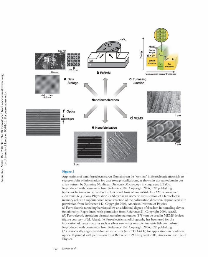
mechanisms behind these properties are still heavily debated (24). Figure 2 sum-marizes some of the applications of nanoferroelectrics.
At the heart of the majority of these applications is ferroelectric polarizationswitching, and much effort has been put forth toward understanding the fundamentalphysics involved, including the nucleation mechanism, discrepancies between pre-dicted and observed coercive fields, loss of polarization due to repeated switchingcycles (fatigue), domain wall width, and minimum stable domain size. In the caseof a capacitor structure with a homogeneous field, the nucleation is initiated at aferroelectric-electrode interface, and a domain grows as an elongated ellipsoid, asfirst described by Landauer (25). Remarkably, the nucleation barriers, or the fieldrequired to nucleate domains predicted by Landauer theory, are much larger thanexperimentally observed, suggesting the existence of defect centers at which nu-cleation is initiated. Several theories have been proposed to address this apparentreduction of the activation barrier, including passive layers (26), tunneling (27), andferroelectric-electrode coupling (28). Despite more than 50 years of extensive studies,the microscopic origins of this Landauer paradox are still unresolved.
Many of the current experimental and theoretical efforts are directed toward thephysics of low-dimensional ferroelectrics (29). Traditionally, piezoelectric couplingin nanocrystalline materials was considered to be analogous to macroscopic materials.For ferroelectrics, the studies of the size effect have centered on the paradigm of theferroelectric bulk and the paraelectric surface layer. The experimental discovery offerroelectric nanotubes (30, 31) in the past several years has prompted theoreticalstudies that predict new types of helical polar ordering in nanoferroelectrics (32). Inaddition, advances in the self-assembly of ferroelectric nanostructures and multifer-roic heterostructures have enabled studies on size effects, constrained systems, andmultiferroic coupling (30, 33–40).
Novel Couplings
Similar to transport, optical, and magnetic phenomena, the nanoscale can also enablecompletely new types of electromechanical behavior. As illustrated by the exampleof a single bond, piezoelectric coupling is a universal feature of polar systems. Forexample, a dipole layer on the surface, such as an ordered water layer, is expected tobe piezoelectric. At the same time, a liquid-like water layer will be nonpiezoelectric.Thus, piezoelectricity can serve as an indication of water state. The significance of
←−−−−−−−−−−−−−−−−−−−−−−−−−−−−−−−−−−−−−−−−−−−−−−−−−−−−−−−−−−−−−−Figure 1Electromechanical coupling on the molecular level. (a) The application of an electric fieldresults in bond contraction or expansion. An electric field acting along the molecule axisinduces an electrostatic force, Fel = 2qE, and the elongation of the molecule isdl = (F + Fel )/k = F/k + 2q E/k. In terms of strain, x = dl/ l . (b) The application of anexternal force results in a change of the dipole moment. If the bond dipoles are parallel, thematerial is piezoelectric. (c) If dipoles are antiparallel, the material is nonpiezoelectric.(d ) More complex dipole arrangements give rise to different coupling. Schematics showing the(e) direct and ( f ) converse piezoelectric effect.
www.annualreviews.org • Nanoelectromechanics of Ferroelectrics and Biosystems 193
Ann
u. R
ev. M
ater
. Res
. 200
7.37
:189
-238
. Dow
nloa
ded
from
ww
w.a
nnua
lrev
iew
s.or
gby
Uni
vers
ity o
f L
eeds
on
05/0
1/13
. For
per
sona
l use
onl
y.
ANRV315-MR37-07 ARI 30 May 2007 21:54
Figure 2Applications of nanoferroelectrics. (a) Domains can be “written” in ferroelectric materials torepresent bits of information for data storage applications, as shown in this nanodomain dotarray written by Scanning Nonlinear Dielectric Microscopy in congruent LiTaO3.Reproduced with permission from Reference 108. Copyright 2006, IOP publishing.(b) Ferroelectrics can be used as the functional basis of nonvolatile FeRAM in consumerelectronics (e.g., Sony PlayStation 2). Shown is an isomeric cross section of a ferroelectricmemory cell with superimposed reconstruction of the polarization direction. Reproduced withpermission from Reference 142. Copyright 2004, American Institute of Physics.(c) Ferroelectric tunneling barriers allow an additional degree of freedom in tunneling devicefunctionality. Reproduced with permission from Reference 21. Copyright 2006, AAAS.(d ) Ferroelectric strontium bismuth tantalate nanotubes (178) can be used in MEMS devices(figure courtesy of M. Alexe). (e) Ferroelectric nanolithography has been used for thefabrication of nanostructures such as silver nanowires on stoichiometric lithium niobate.Reproduced with permission from Reference 167. Copyright 2006, IOP publishing.( f ) Periodically engineered domain structures (in RbTiOAsO4) for applications in nonlinearoptics. Reprinted with permission from Reference 179. Copyright 2003, American Institute ofPhysics.
194 Kalinin et al.
Ann
u. R
ev. M
ater
. Res
. 200
7.37
:189
-238
. Dow
nloa
ded
from
ww
w.a
nnua
lrev
iew
s.or
gby
Uni
vers
ity o
f L
eeds
on
05/0
1/13
. For
per
sona
l use
onl
y.
ANRV315-MR37-07 ARI 30 May 2007 21:54
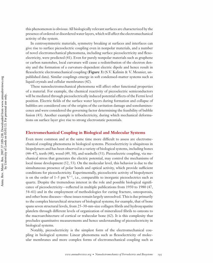
this phenomenon is obvious: All biologically relevant surfaces are characterized by thepresence of ordered or disordered water layers, which will affect the electromechanicalactivity of the system.
In centrosymmetric materials, symmetry breaking at surfaces and interfaces cangive rise to surface piezoelectric coupling even in nonpolar materials, and a numberof novel electromechanical phenomena, including surface piezoelectricity and flexo-electricity, were predicted (41). Even for purely nonpolar materials such as grapheneor carbon nanotubes, local curvature will cause a redistribution of the electron den-sity and the formation of a curvature-dependent electric dipole and hence result inflexoelectric electromechanical coupling (Figure 3) (S.V. Kalinin & V. Meunier, un-published data). Similar couplings emerge in soft condensed-matter systems such asliquid crystals and cellular membranes (42).
These nanoelectromechanical phenomena will affect other functional propertiesof a material. For example, the chemical reactivity of piezoelectric semiconductorswill be mediated through piezoelectrically induced potential effects of the Fermi levelposition. Electric fields of the surface water layers during formation and collapse ofbubbles are considered one of the origins of the cavitation damage and sonolumines-cence and were considered the governing factor determining the feasibility of bubblefusion (43). Another example is triboelectricity, during which mechanical deforma-tions on surface layer give rise to strong electrostatic potentials.
Electromechanical Coupling in Biological and Molecular Systems
Even more common and at the same time more difficult to assess are electrome-chanical coupling phenomena in biological systems. Piezoelectricity is ubiquitous inbiopolymers and has been observed in a variety of biological systems, including bones(44–47), teeth (48), wood (49, 50), and seashells (51). Piezoelectric coupling, via me-chanical stress that generates the electric potential, may control the mechanisms oflocal tissue development (52, 53). On the molecular level, this behavior is due to thesimultaneous presence of polar bonds and optical activity, which provide sufficientconditions for piezoelectricity. Experimentally, piezoelectric activity of biopolymersis on the order of 1–5 pm V−1, i.e., comparable to inorganic piezoelectrics such asquartz. Despite the tremendous interest in the role and possible biological signifi-cance of piezoelectricity—reflected in multiple publications from 1950 to 1980 (47,54–61) and in the employment of methodologies for curing fracture, osteoporosis,and other bone diseases—these issues remain largely unresolved. This is due primarilyto the complex hierarchical structure of biological systems; for example, that of bonespans seven structural levels, from 25–30-nm-size collagen fibrils and hydroxyapatiteplatelets through different levels of organization of mineralized fibrils to osteons tothe macroarchitecture of cortical or trabecular bone (62). It is this complexity thatprecludes quantitative measurements and hence understanding of piezoelectricity inbiological systems.
Notably, piezoelectricity is the simplest form of the electromechanical cou-pling in biological systems: Linear phenomena such as flexoelectricity of molec-ular membranes and more complex forms of electromechanical coupling such as
www.annualreviews.org • Nanoelectromechanics of Ferroelectrics and Biosystems 195
Ann
u. R
ev. M
ater
. Res
. 200
7.37
:189
-238
. Dow
nloa
ded
from
ww
w.a
nnua
lrev
iew
s.or
gby
Uni
vers
ity o
f L
eeds
on
05/0
1/13
. For
per
sona
l use
onl
y.

ANRV315-MR37-07 ARI 30 May 2007 21:54
Figure 3Electromechanical phenomena on the nanoscale. (a) Nonferroelectric surface layers andhelical ordering in ferroelectric nanoclusters, (b) flexoelectricity and electromotor proteins incellular membranes, ordered water layers in (c) nanocomposites and (d ) on surfaces, and(e) quantum flexoelectricity in graphene.
196 Kalinin et al.
Ann
u. R
ev. M
ater
. Res
. 200
7.37
:189
-238
. Dow
nloa
ded
from
ww
w.a
nnua
lrev
iew
s.or
gby
Uni
vers
ity o
f L
eeds
on
05/0
1/13
. For
per
sona
l use
onl
y.
ANRV315-MR37-07 ARI 30 May 2007 21:54
Piezoresponse forcemicroscopy (PFM):scanning probe techniquebased on the detection ofthe electromechanicalresponse of a material to anapplied electrical bias
Vector PFM: thereal-space reconstruction ofelectromechanical responsevector and localcrystallographic orientationfrom three components ofpiezoresponse: vertical PFMand two orthogonal lateralPFM components
SPM: scanning probemicroscopy
Piezoelectric surface: a3-D plot depicting thepiezoresponse as a functionof the angle between thedirection of the applied fieldand the measurement axis
voltage-controlled muscular contractions (63), cell electromotility (64), and electro-motor proteins (65) are ubiquitous. In many cases, these couplings are the functionalbases for processes such as transduction of acoustic signals into electrical pulses in theouter hair cell stereocilia (hearing), transport in ion channels, energy storage in mi-tochondria, cardiac myocyte activity, etc. Understanding local electromechanics, inaddition to electrochemistry, is one of the key challenges in understanding biologicalsystems.
To complement biological systems, in the past several years the concept of elec-trically driven molecular machines, in which electrochemical transformations inducea set of changes in bonding configurations leading to a change in molecular confor-mations, has emerged (66).
NANOSCALE PROBING OF ELECTROMECHANICALCOUPLING
Despite the rich gamut of novel electromechanical phenomena existing on thenanoscale and their relevance for areas as diversified as biological systems, energyharvesting materials, and computer memories, virtually no information is availableexperimentally. The reasons behind this dearth of information are straightforward—many of these effects manifest on length scales well below micron and often on theorder of nanometers, comparable to molecular sizes. Electromechanical measure-ments at these length scales require either currents on the order of ∼femtoamperesor displacements on the order of ∼picometers probed over areas of ∼10–1000 nm2,considered impossible until recently. The breakthrough in this direction has comewith the advent of piezoresponse force microscopy (PFM) (67–71), which utilizes theconverse piezoeffect to image local polarization orientation. Below, we discuss thebasic principles of PFM and compare the image formation mechanism in PFM withthat of other scanning probe microscopy (SPM) techniques.
Principles of PFM
PFM is based on the detection of bias-induced piezoelectric surface deforma-tion. The tip is brought into contact with the surface, and the local piezoelec-tric response is detected as the first harmonic component, A1ω, of the tip de-flection, A = A0 + A1ωcos (ωt + ϕ), during the application of the periodic biasVtip = Vdc + Vaccos (ωt) to the tip. The phase of the electromechanical responseof the surface, ϕ, yields information on the polarization direction below the tip. Forc− domains (polarization vector oriented normal to the surface and pointing down-ward), the application of a positive tip bias results in the expansion of the sample,and surface oscillations are in phase with the tip voltage, ϕ = 0. For c+ domains,ϕ = 180◦. The piezoresponse amplitude, A = A1ω/Vac, given in units of nanometersper volt, defines the local electromechanical activity. PFM images can be conve-niently represented as A1ωcos (ϕ)
/Vac, where A1ω is the amplitude of first harmonic
of measured response (in nanometers), provided that the phase signal varies by 180◦
between domains of opposite polarities. Detection of the torsional components of tip
www.annualreviews.org • Nanoelectromechanics of Ferroelectrics and Biosystems 197
Ann
u. R
ev. M
ater
. Res
. 200
7.37
:189
-238
. Dow
nloa
ded
from
ww
w.a
nnua
lrev
iew
s.or
gby
Uni
vers
ity o
f L
eeds
on
05/0
1/13
. For
per
sona
l use
onl
y.

ANRV315-MR37-07 ARI 30 May 2007 21:54
STM: scanning tunnelingmicroscopy
AFM: atomic forcemicroscopy
vibrations provides information on the in-plane surface displacement, referred to aslateral PFM. A third component of the displacement vector can be determined byimaging the same region of the sample after rotation by 90◦ (72). Provided that thevertical and lateral PFM signals are properly calibrated, the complete electromechan-ical response vector can be determined, an approach referred to as vector PFM (73).Finally, electromechanical response can be probed as a function of DC bias of thetip, providing information on polarization switching in ferroelectrics as well as morecomplex electrochemical and electrocapillary processes in the tip-surface junction(74, 75).
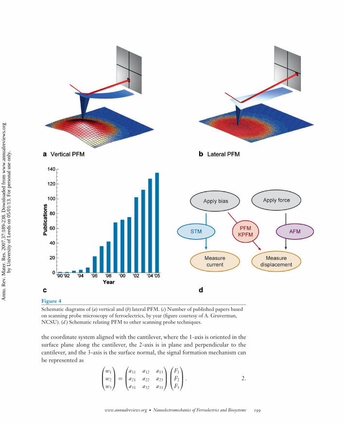
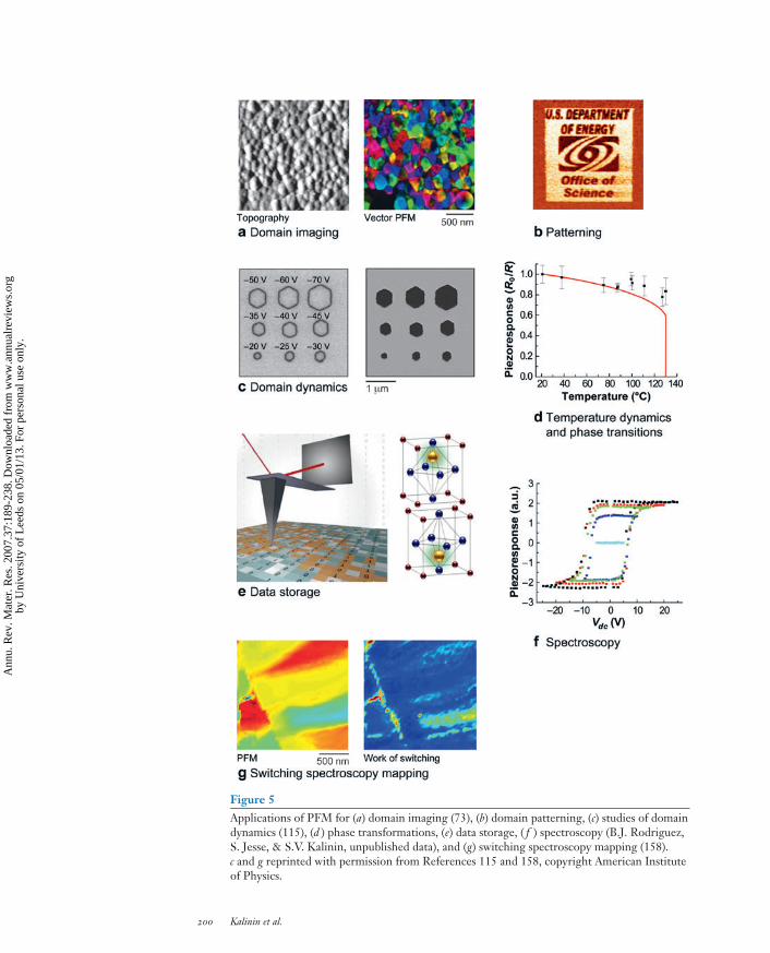
In the decade since its invention, PFM has been established as a powerful tool forprobing local electromechanical activity on the nanometer scale (76–79). Developedoriginally for imaging domain structures in ferroelectric materials, PFM was laterextended to local hysteresis loop spectroscopy (39, 80) and ferroelectric domain pat-terning for applications such as high-density data storage (81, 82) and ferroelectriclithography (83–85). The broad applicability of PFM to materials such as ferroelectricperovskites, piezoelectric III-V nitrides (86), and, recently, biological systems suchas calcified and connective tissues (87–89) has resulted in an increasing number ofpublications, as illustrated in Figure 4c. Various applications of PFM are shown inFigure 5.
PFM versus Other SPMs
The fundamental factors underpinning any SPM method are (a) the tensorial nature ofthe signal, (b) the signal dependence on contact radius (contact modes) or tip-surfaceseparation (noncontact modes), and (c) the signal dependence on the cantilever springconstant. These factors determine the strategies for instrumentation and techniquedevelopment and the potential for quantitative measurements.
In current-based techniques such as scanning tunneling microscopy (STM) andconductive atomic force microscopy (AFM), the excitation signal (applied bias) anddetected signal (current magnitude) are scalar quantities. Hence, the response isscalar,
I = �V, 1.
where � is the local conductance. The conductance scales with the contact area as� ∼ a1 in the classical (Maxvell) regime (90) and � ∼ a2 in the Sharvin regime(91). Hence, image contrast can be induced either by variation in specific resistanceor by contact radius, e.g., owing to variations in surface topography (cross talk).When the contact is confined to a single atom in a tunneling regime, � ∼ a0. Inmost applications of conductive AFM, the variations in local conductivities betweendissimilar materials (e.g., differently doped regions of a semiconductor) dominaterelatively small changes in contact geometry, the condition ensured by operation atlarge indentation forces on planar substrates. This, in turn, allows for calibration andquantitative measurements using current-based techniques.
In force-based techniques, both the excitation signal (force) and the responsesignal (displacement) are vectors. Hence, the AFM signal is a rank-two tensor. In
198 Kalinin et al.
Ann
u. R
ev. M
ater
. Res
. 200
7.37
:189
-238
. Dow
nloa
ded
from
ww
w.a
nnua
lrev
iew
s.or
gby
Uni
vers
ity o
f L
eeds
on
05/0
1/13
. For
per
sona
l use
onl
y.
ANRV315-MR37-07 ARI 30 May 2007 21:54
Figure 4Schematic diagrams of (a) vertical and (b) lateral PFM. (c) Number of published papers basedon scanning probe microscopy of ferroelectrics, by year (figure courtesy of A. Gruverman,NCSU). (d ) Schematic relating PFM to other scanning probe techniques.
the coordinate system aligned with the cantilever, where the 1-axis is oriented in thesurface plane along the cantilever, the 2-axis is in plane and perpendicular to thecantilever, and the 3-axis is the surface normal, the signal formation mechanism canbe represented as ⎛
⎜⎝w1
w2
w3
⎞⎟⎠ =
⎛⎜⎝a11 a12 a13
a21 a22 a23
a31 a32 a33
⎞⎟⎠
⎛⎜⎝F1
F2
F3
⎞⎟⎠ . 2.
www.annualreviews.org • Nanoelectromechanics of Ferroelectrics and Biosystems 199
Ann
u. R
ev. M
ater
. Res
. 200
7.37
:189
-238
. Dow
nloa
ded
from
ww
w.a
nnua
lrev
iew
s.or
gby
Uni
vers
ity o
f L
eeds
on
05/0
1/13
. For
per
sona
l use
onl
y.
ANRV315-MR37-07 ARI 30 May 2007 21:54
Figure 5Applications of PFM for (a) domain imaging (73), (b) domain patterning, (c) studies of domaindynamics (115), (d ) phase transformations, (e) data storage, ( f ) spectroscopy (B.J. Rodriguez,S. Jesse, & S.V. Kalinin, unpublished data), and (g) switching spectroscopy mapping (158).c and g reprinted with permission from References 115 and 158, copyright American Instituteof Physics.
200 Kalinin et al.
Ann
u. R
ev. M
ater
. Res
. 200
7.37
:189
-238
. Dow
nloa
ded
from
ww
w.a
nnua
lrev
iew
s.or
gby
Uni
vers
ity o
f L
eeds
on
05/0
1/13
. For
per
sona
l use
onl
y.

ANRV315-MR37-07 ARI 30 May 2007 21:54
The component of the stiffness tensor a33 is probed by conventional vertical AFMand atomic force acoustic microscopy (AFAM), whereas a22 is probed by lateral forcemicroscopy. The off-diagonal component, a23 and a32, represents coupling betweenthe vertical and lateral signals. However, a conventional cantilever sensor does notallow the separation of the normal and longitudinal force components, both of whichresult in a flexural deformation of the cantilever. Hence, SPM flexural, fl, and tor-sional, tr , responses are related to force components as
(fltr
)=
(αa11 + βa31 αa12 + βa32 αa13 + βa33
χa21 χa22 χa23
) ⎛⎜⎝F1
F2
F3
⎞⎟⎠ , 3.
where α, β, and χ are proportionality coefficients dependent on cantilever geometryand detector calibration.
In the continuum mechanics limit, the contact stiffnesses are proportional to thecontact radius, ai j ∼ a1. When the contact area is a single molecule, as in proteinunfolding spectroscopy, or a single atom, as in atomic resolution imaging, ai j ∼ a0.Hence, quantitative force measurements are generally limited to when the contactgeometry is well characterized, as in nanoindentation techniques, or is weakly depen-dent on the probe, as in molecular unfolding spectroscopy. In other cases, the changesin contact stiffness represent the convolution of variation in local elastic propertiesand surface topography (topographic cross talk).
Most force sensors have well-defined resonant behavior: Corresponding resonantfrequencies are determined by the spring constant of the system and tip-surfacejunction. This enables a broad range of imaging techniques based on the resonantenhancement of cantilever oscillations, frequency tracking methods, etc. In particular,contact resonant frequency in techniques such as vertical and lateral AFAM is directlyrelated to the contact stiffnesses as determined by local elastic properties (primarysignal) and topography (cross talk).
Finally, in PFM the excitation signal is scalar, whereas the electromechanical re-sponse of the surface is a vector. Hence, the PFM response is a vector,⎛
⎜⎝w1
w2
w3
⎞⎟⎠ =
⎛⎜⎝d1
d2
d3
⎞⎟⎠V. 4.
Here, the response components di describe the electromechanical coupling in the ma-terial in the point contact geometry. As for AFM, the vertical and longitudinal surfacedisplacements contribute to the flexural vibration of the cantilever, and strategies toovercome this limitation are considered below. The distinctive feature of the elec-tromechanical response is dependence on contact area. From simple dimensionalityconsiderations, the electromechanical response does not depend on the contact area,di ∼ a0, as confirmed by rigorous theory for special classes of materials symmetry(92, 93).
This weak dependence of the PFM signal on the contact area suggests that (a) elec-tromechanical measurements are intrinsically quantitative (if good tip-surface con-tact is achieved) and do not require extensive probe calibration and that (b) signal is
www.annualreviews.org • Nanoelectromechanics of Ferroelectrics and Biosystems 201
Ann
u. R
ev. M
ater
. Res
. 200
7.37
:189
-238
. Dow
nloa
ded
from
ww
w.a
nnua
lrev
iew
s.or
gby
Uni
vers
ity o
f L
eeds
on
05/0
1/13
. For
per
sona
l use
onl
y.

ANRV315-MR37-07 ARI 30 May 2007 21:54
EFM: electrostatic forcemicroscopy
KPFM: Kelvin probe forcemicroscopy
relatively insensitive to topographic cross talk. However, resonance enhancement can-not be directly employed in PFM because the resonance frequency is determined bymechanical, rather than electromechanical, properties of material. Finally, quadraticbias dependence of electrostatic forces, as compared with linear piezoelectric inter-actions, suggests that the electromechanical signal cannot be unambiguously distin-guished from the electrostatic signal. These considerations determine limitations andsuggest strategies for improving PFM resolution and sensitivity, as discussed below(see section on Future Directions in PFM).
PFM ON PIEZOELECTRIC MATERIALS
The primary factors determining the imaging mechanism in PFM are (a) voltage-dependent contact mechanics of the tip-surface junction, including the relationshipbetween local surface displacement and material properties, and displacements in thevicinity of microstructural elements such as domain walls, (b) dynamic behavior of thecantilever, including the relationship between surface displacement vector and tor-sional and flexural vibrations of the cantilever, and (c) the electroelastic field structureinside the material that determines spatial resolution and switching processes. Below,we consider the contrast formation mechanism, cantilever dynamics and resonanceenhancement, and the role of electrostatic interactions in PFM.
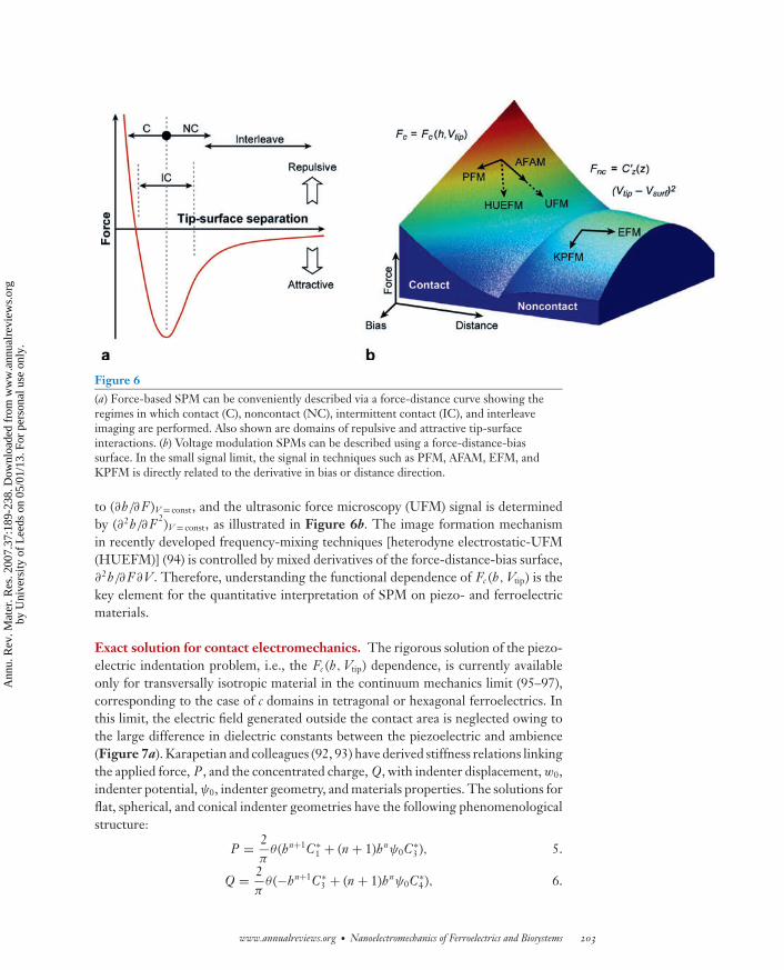
Contact Mechanics of Piezoelectric Indentation
General formulation. Traditionally, principles and physical underpinnings of SPMtechniques can be conveniently understood using force-distance curves (Figure 6a).Depending on the dominant interactions, AFM can be sensitive to elastic interac-tions (e.g., AFAM), Van der Waals interactions (noncontact AFM), and magnetic andelectrostatic forces [e.g., electrostatic force microscopy (EFM)]. A similar approachcan be used for voltage modulation techniques such as PFM. However, here the sys-tem is described by two independent variables, tip-surface separation and tip bias,giving rise to force-distance-bias surface, as depicted in Figure 6b. In the noncontactregime, the tip-surface forces are purely capacitive, and the shape of the surface isdescribed by Fnc = C ′
z(z)(Vtip − Vsurf)2, where C ′z(z) is the tip-surface capacitance gra-
dient. Kelvin probe force microscopy (KPFM) is sensitive to the voltage derivative ofthe force, ∂ Fnc
/∂Vtip. The known functional form of this dependence renders KPFM
readily interpretable and relatively insensitive to topographic artifacts. At the sametime, techniques such as EFM are sensitive to the distance derivative of capacitance,and the presence of the (unknown) C ′
z(z) term makes quantitative interpretation ofEFM more challenging, at the same time rendering technique more sensitive to to-pographic cross talk.
In the contact regime, the imaging mechanism of SPM is ultimately controlledby the shape of the force-distance-bias surface, i.e., Fc = Fc (h, Vtip), where h isthe indentation depth. The image formation mechanism in various SPM techniquescan be related to the derivatives of this surface. For example, in the small signalapproximation the PFM signal is given by (∂h/∂Vtip)F = const, the AFAM signal is related
202 Kalinin et al.
Ann
u. R
ev. M
ater
. Res
. 200
7.37
:189
-238
. Dow
nloa
ded
from
ww
w.a
nnua
lrev
iew
s.or
gby
Uni
vers
ity o
f L
eeds
on
05/0
1/13
. For
per
sona
l use
onl
y.
ANRV315-MR37-07 ARI 30 May 2007 21:54
Figure 6(a) Force-based SPM can be conveniently described via a force-distance curve showing theregimes in which contact (C), noncontact (NC), intermittent contact (IC), and interleaveimaging are performed. Also shown are domains of repulsive and attractive tip-surfaceinteractions. (b) Voltage modulation SPMs can be described using a force-distance-biassurface. In the small signal limit, the signal in techniques such as PFM, AFAM, EFM, andKPFM is directly related to the derivative in bias or distance direction.
to (∂h/∂ F )V = const, and the ultrasonic force microscopy (UFM) signal is determinedby (∂2h/∂ F 2)V = const, as illustrated in Figure 6b. The image formation mechanismin recently developed frequency-mixing techniques [heterodyne electrostatic-UFM(HUEFM)] (94) is controlled by mixed derivatives of the force-distance-bias surface,∂2h/∂ F∂V . Therefore, understanding the functional dependence of Fc (h, Vtip) is thekey element for the quantitative interpretation of SPM on piezo- and ferroelectricmaterials.
Exact solution for contact electromechanics. The rigorous solution of the piezo-electric indentation problem, i.e., the Fc (h, Vtip) dependence, is currently availableonly for transversally isotropic material in the continuum mechanics limit (95–97),corresponding to the case of c domains in tetragonal or hexagonal ferroelectrics. Inthis limit, the electric field generated outside the contact area is neglected owing tothe large difference in dielectric constants between the piezoelectric and ambience(Figure 7a). Karapetian and colleagues (92, 93) have derived stiffness relations linkingthe applied force, P , and the concentrated charge, Q, with indenter displacement, w0,indenter potential, ψ0, indenter geometry, and materials properties. The solutions forflat, spherical, and conical indenter geometries have the following phenomenologicalstructure:
P = 2π
θ (hn+1C∗1 + (n + 1)hnψ0C∗
3 ), 5.
Q = 2π
θ (−hn+1C∗3 + (n + 1)hnψ0C∗
4 ), 6.
www.annualreviews.org • Nanoelectromechanics of Ferroelectrics and Biosystems 203
Ann
u. R
ev. M
ater
. Res
. 200
7.37
:189
-238
. Dow
nloa
ded
from
ww
w.a
nnua
lrev
iew
s.or
gby
Uni
vers
ity o
f L
eeds
on
05/0
1/13
. For
per
sona
l use
onl
y.
ANRV315-MR37-07 ARI 30 May 2007 21:54
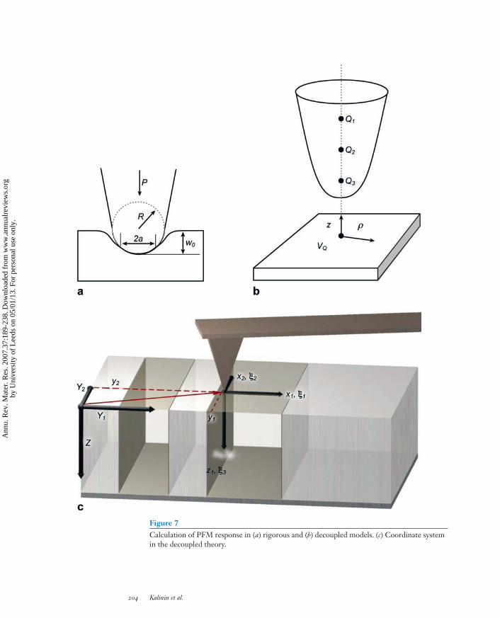
Figure 7Calculation of PFM response in (a) rigorous and (b) decoupled models. (c) Coordinate systemin the decoupled theory.
204 Kalinin et al.
Ann
u. R
ev. M
ater
. Res
. 200
7.37
:189
-238
. Dow
nloa
ded
from
ww
w.a
nnua
lrev
iew
s.or
gby
Uni
vers
ity o
f L
eeds
on
05/0
1/13
. For
per
sona
l use
onl
y.

ANRV315-MR37-07 ARI 30 May 2007 21:54
where h is the total indenter displacement, θ is a geometric factor [θ = a for flatindenters, θ = (2/3)R1/2 for spherical indenters, and θ = (1/π ) tan α for conicalindenters] and n = 0 for flat, n = 1/2 for spherical, and n = 1 for conical indenters,respectively.
These stiffness relations provide an extension of the corresponding results ofHertzian mechanics and continuum electrostatics to the transversely isotropic piezo-electric medium. From this analysis, the maximum information that can be obtainedfrom SPM or nanoindentation is limited to the indentation elastic stiffness, C∗
1 , theindentation piezocoefficient, C∗
3 , and the indentation dielectric constant, C∗4 . Inden-
tation stiffnesses are complex functions of electroelastic constants of the material,C∗
i = C∗i (c i j , ei j , εi j ), where c i j are elastic stiffnesses, ei j are piezoelectric constants,
and εi j are dielectric constants. Experimentally, AFAM and UFM response is deter-mined by C∗
1 , whereas PFM is sensitive to C∗3/C∗
1 . For most materials, C∗3/C∗
1 ∼ d33
and C∗4 ≈ √
ε11ε33 (92, 93). The electroelastic fields produced by the indentor rapidlyadopt the form of the point charge/point force at distances comparable to the contactradius.
Decoupling approximation in contact electromechanics. The necessity for cal-culating the PFM signal for materials of general symmetry, as well as calculating theresponse at microstructural elements such as domain walls, cylindrical domains, andtopographically inhomogeneous ferroelectrics such as nanoparticles, has stimulatedtheoretical attempts to derive approximate solutions for PFM contrast.
A general approach for the calculation of the electromechanical response is basedon the decoupling approximation. In this case, (a) the electric field in the material iscalculated using a rigid electrostatic model (no piezoelectric coupling, di jk = ei jk = 0),(b) the strain or stress field is calculated using constitutive relations for a piezoelec-tric material, Xi j = Ekeki j , and (c) the displacement field is evaluated using the ap-propriate Green’s function for an isotropic or anisotropic solid. Ganpule et al. (98)originally suggested a simplified 1-D version of the decoupled model to accountfor the effect of 90◦ domain walls on PFM imaging. Agronin et al. (99) adapteda similar 1-D approach to yield closed-form solutions for the PFM signal. Feltenet al. (100) developed the 3-D version of the decoupled model, using the analyt-ical form for the corresponding Green’s function. Independently, Scrymgeour &Gopalan (101) used the finite element method to model PFM signals across domainwalls. Recently, Kalinin et al. (102), Eliseev et al. (103), and Morozovska et al. (104)applied the decoupled theory to derive analytical expressions for PFM response onmaterials of low symmetry, derive analytical expressions for PFM resolution func-tion and domain wall profiles, and interpret PFM spectroscopy data, as describedbelow.
In the decoupled approximation, the PFM signal, i.e., the surface displacementui
(x, y
)at location x induced by the tip at position y = ( y1, y2), is given by
ui (x, y) =∫ ∞
−∞dξ1
∫ ∞
−∞dξ2
∫ ∞
0dξ3
∂Gi j (x1 − ξ1, x2 − ξ2, ξ3)∂ξk
×El (ξ)c kjmndln m(y1 + ξ1, y2 + ξ2, ξ3). 7.
www.annualreviews.org • Nanoelectromechanics of Ferroelectrics and Biosystems 205
Ann
u. R
ev. M
ater
. Res
. 200
7.37
:189
-238
. Dow
nloa
ded
from
ww
w.a
nnua
lrev
iew
s.or
gby
Uni
vers
ity o
f L
eeds
on
05/0
1/13
. For
per
sona
l use
onl
y.

ANRV315-MR37-07 ARI 30 May 2007 21:54
PZT: lead zirconatetitanate
Here coordinate x = (x1, x2, z) is linked to the indentor apex, and coordinatesy = ( y1, y2) denote indentor position in the sample coordinate system y (Figure 7b).The integration is performed over the spatial coordinates (ξ1, ξ2, ξ3). Coefficients dmnk
and cjlmn are position-dependent components of the piezoelectric strain constant andelastic stiffness tensors, respectively. Ek (x) is the electric field distribution producedby the probe. The Green’s function for a semi-infinite medium G3 j (x − ξ ) links theeigenstrains c j lmndmnk Ek to the displacement field. This approach is rigorous for ma-terials with small piezoelectric coefficients. A simple estimation of the decouplingapproximation applicability is based on the value of the square of the dimensionlesselectromechanical coupling coefficients k2
i j = (di j )2/(s j j εi i ). For instance, for BaTiO3,k2
15 ≈ 0.32, k231 ≈ 0.10, and k2
33 ≈ 0.31; for the ceramics lead zirconate titanate(PZT) 6B, k2
15 ≈ 0.14, k231 ≈ 0.02, and k2
33 ≈ 0.13; and for a quartz single crystal,k2
11 ≈ 0.01. This suggests that the error in the decoupling approximation does notexceed ∼30% for strongly piezoelectric materials and is on the order of ∼1% for weakpiezoelectrics.
Approximate solution for piezoresponse of homogeneous media. The use of the de-coupling approximation reduces an extremely complex coupled contact mechanicsproblem to the solutions of much simpler electrostatic and mechanical Green’s func-tion problems and numerical integration of the result. The dielectric and particularlyelastic properties described by positively defined second- and fourth-rank tensors (in-variant with respect to 180◦ rotation) are necessarily more isotropic than the piezo-electric properties described by third-rank tensors (antisymmetric with respect to180◦ rotation). Hence, elastic and dielectric properties of a material can often beapproximated as isotropic. In this case, integrals in Equation 7 can be evaluated, andsurface displacement can be written in the form ui (x) = VQWi jlk (x) dkjl , where thetensor Wi jlk (x) is symmetrical on the transposition of the indexes j and l . In Voigtnotation, the displacements are (102)
u1 (0) = VQ (W111d11 + W121d12 + W131d13 + W153d35 + W162d26) , 8a.
u2 (0) = VQ (W121d21 + W111d22 + W131d23 + W153d34 + W162d16) , 8b.
u3 (0) = VQ (W313 (d31 + d32) + W333d33 + W351 (d24 + d15)) . 8c.
The nonzero elements of the tensor Wiαk are W111 = −(13 + 4ν)/32, W121 = (1 −12ν)/32, W131 = −1/8, W153 = −3/8, W162 = −(7 − 4ν)/32, W313 = −(1 + 4ν)/8,W333 = −3/4, W351 = −1/8. Here VQ is the electrostatic potential in the pointx = (0, 0, 0) produced by a probe represented by the set of image charges locatedon a vertical line. Thus, the response is shown to be proportional to the potentialinduced by the tip on the surface. The latter fundamental result was generalized asresponse theorems (103).
1. Response theorem 1: For a transversally isotropic piezoelectric solid in anisotropic elastic approximation and an arbitrary point-charge distribution inthe tip (not necessarily constrained to a single line), the vertical surface dis-placement is proportional to the surface potential induced by tip charges in thepoint of contact.
206 Kalinin et al.
Ann
u. R
ev. M
ater
. Res
. 200
7.37
:189
-238
. Dow
nloa
ded
from
ww
w.a
nnua
lrev
iew
s.or
gby
Uni
vers
ity o
f L
eeds
on
05/0
1/13
. For
per
sona
l use
onl
y.

ANRV315-MR37-07 ARI 30 May 2007 21:54
2. Response theorem 2: For an anisotropic piezoelectric solid in the limit of dielec-tric and elastic isotropy, the vertical and lateral PFM signals are proportional tothe potential on the surface induced by the tip if the tip charges and the pointof contact are located on the same line along the surface normal.
For lower material symmetries, the analytical expressions of the displacementfields induced by the point charge allow response calculations for asymmetric tips orprobes with special geometry (103).
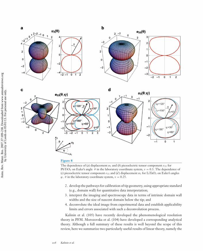
Orientational imaging. In piezoelectric materials, the strong orientation depen-dence of the electromechanical response opens the pathway to orientation imaging.Briefly, the orientation of a molecule or crystallographic lattice with respect to thelaboratory coordinate system is given by three Euler angles (θ, ϕ, ψ). The relation-ship between the di jk tensor in the laboratory coordinate system and the d 0
i j k tensorin the crystal coordinate system is di jk = Ail Ajm Aknd 0
lmn, where Ai j (θ, ϕ, ψ) is the ro-tation matrix (10). Experimentally, PFM measures three components of the responsevector. Hence, local crystallographic orientation can be determined from the solu-tions of Equation 8, which can graphically be represented as response surfaces. As anexample, we compare vertical displacement u3 surfaces with piezoelectric tensors d33
surfaces for the tetragonal PbTiO3 and trigonal LiTaO3 model systems in Figure 8(103). In this analysis the dielectric properties of the material were assumed to beclose to isotropic, and hence the electric field distribution is insensitive to sample ori-entation. However, a similar analysis can be performed for full dielectric and elasticanisotropy.
Linear Imaging Theory in PFM
The remarkable characteristic of the signal formation mechanism in PFM given byEquation 7 is its linearity. In particular, if the sample is uniform in the z-direction onthe scale of the penetration depth of electric field, i.e., c jlmndmnk(x, z) ≈ c jlmndmnk(x),vertical surface displacement below the tip, i.e., vertical PFM signal, can be rewrittenas
u3(0, y
) =∫ ∞
−∞dmnk
(y − ξ
) (∫ ∞
z=0c j lmn Ek (−ξ1, −ξ2, z)
∂
∂ξlG3 j (ξ1, ξ2, z) d z
)dξ1dξ2,
9.i.e., as a convolution of a function describing the spatial distribution of materialproperties, dmnk (x), and a resolution function related to probe parameters (integralin parenthesis).
Image formation described by Equation 9 belongs to the class of so-called linearimaging mechanisms. Linearity of the PFM image formation mechanism allows oneto
1. establish the unambiguous definitions for spatial resolution (minimal featuresize required for quantitative response measurements) and information lim-its (minimal detectable feature size) and its dependence on tip geometry andmaterials properties, suggesting strategies for high-resolution imaging;
www.annualreviews.org • Nanoelectromechanics of Ferroelectrics and Biosystems 207
Ann
u. R
ev. M
ater
. Res
. 200
7.37
:189
-238
. Dow
nloa
ded
from
ww
w.a
nnua
lrev
iew
s.or
gby
Uni
vers
ity o
f L
eeds
on
05/0
1/13
. For
per
sona
l use
onl
y.
ANRV315-MR37-07 ARI 30 May 2007 21:54
Figure 8The dependence of (a) displacement u3 and (b) piezoelectric tensor component e33 forPbTiO3 on Euler’s angle θ in the laboratory coordinate system, ν = 0.3. The dependence of(c) piezoelectric tensor component e33 and (d ) displacement u3 for LiTaO3 on Euler’s anglesϕ, θ in the laboratory coordinate system, ν = 0.25.
2. develop the pathways for calibration of tip geometry, using appropriate standard(e.g., domain wall) for quantitative data interpretation;
3. interpret the imaging and spectroscopy data in terms of intrinsic domain wallwidths and the size of nascent domain below the tip; and
4. deconvolute the ideal image from experimental data and establish applicabilitylimits and errors associated with such a deconvolution process.
Kalinin et al. (105) have recently developed the phenomenological resolutiontheory in PFM. Morozovska et al. (104) have developed a corresponding analyticaltheory. Although a full summary of these results is well beyond the scope of thisreview, here we summarize two particularly useful results of linear theory, namely the
208 Kalinin et al.
Ann
u. R
ev. M
ater
. Res
. 200
7.37
:189
-238
. Dow
nloa
ded
from
ww
w.a
nnua
lrev
iew
s.or
gby
Uni
vers
ity o
f L
eeds
on
05/0
1/13
. For
per
sona
l use
onl
y.
ANRV315-MR37-07 ARI 30 May 2007 21:54
analytical expression for 180◦ domain wall profile in the point-charge tip limit
u3 (s , Q, d ) = Q2πε0 (εe + κ) d
{g313 (s ) d31 + g351 (s ) d15 + g333 (s ) d33} , 10.
where s = (a − a0)/d is the coordinate along the domain wall normalized by charge-surface separation. The functions gi jk (s ) are simple analytical functions of the dielec-tric anisotropy factor. Equation 10 allows the parameters of the set of image charges{Qm, dm}N representing the tip (S. Jesse, S.V. Kalinin, B.J. Rodriguez, E.A. Eliseev, &A.N. Morozovska, unpublished data) to be determined, i.e., allows probe calibration.
In the context of PFM spectroscopy, the signal in the center of a cylindrical domaincan be found as
d eff33 ≈ −
[34
(d33 +
(13
+ 43ν
)d31
)πd − 8rπd + 8r
+ d15
43πd − 8r3πd + 8r
]. 11.
Here r is the domain radius, and d is charge-surface separation. Equation 11 is de-rived for weak dielectric anisotropy (γ = 1). Through Equation 11 the geometricparameters of the domain formed below the tip can be determined, allowing the de-convolution of the PFM spectroscopy data. The combination of Equations 10 and 11allows self-consistent analysis of PFM switching measurements, in which geometricparameters of the probe derived from the domain wall profile are used to quanti-tatively reconstruct the size of the cylindrical domain formed below the tip in thespectroscopic measurements.
Cantilever Dynamics and Effect of Electrostatic Forces
Jesse et al. (106) have performed a complete analysis of the dynamic image formationmechanisms in vector PFM, including (a) the local vertical surface displacementtranslated to the tip, (b) the longitudinal, in-plane surface displacement along thecantilever axis, (c) the lateral surface displacement, in-plane and perpendicular to thecantilever axis, (d ) the local electrostatic force acting on the tip, and (e) the distributedelectrostatic force acting on the cantilever. Jesse et al. have also described an approachfor deconvolution of electrostatic and electromechanical contributions based on the 2-D response–DC bias–frequency spectroscopy. B. Mirman (unpublished data) derivedthe solution in the presence of surface, cantilever, and hydrodynamics damping.
In particular, in the case of transversally isotropic material (for which displacementvector and tip axis are normal to the surface), the response in the low-frequency regimeis a sum of electromechanical and local and nonlocal electrostatic components as
PR = d1ω
Vac= αa (h)d1
k1
k1 + k+
C ′sphere + C ′
cone
k1 + k(Vdc − Vs ) + C ′
cant
24k(Vdc − Vav). 12.
The first term in Equation 12 is the electromechanical response determined bythe effective piezoresponse coefficient of material, d1, and the ratio of AC potentialon the surface and AC bias applied to the tip (i.e., the potential drop in the tip-surfacegap of thickness, h), αa (h). The second and third terms are local and nonlocal contri-butions due to electrostatic tip-surface and cantilever-surface interactions. The signaltransduction between the surface displacements and electrostatic forces and flexural
www.annualreviews.org • Nanoelectromechanics of Ferroelectrics and Biosystems 209
Ann
u. R
ev. M
ater
. Res
. 200
7.37
:189
-238
. Dow
nloa
ded
from
ww
w.a
nnua
lrev
iew
s.or
gby
Uni
vers
ity o
f L
eeds
on
05/0
1/13
. For
per
sona
l use
onl
y.

ANRV315-MR37-07 ARI 30 May 2007 21:54
Shielded probe: aconducting probe tipsurrounded by insulatingmaterial and groundedcounterelectrode that allowsa highly localized electricfield to be applied
Polarization-dependentphotodeposition: processduring which an ultravioletlight with an energy largerthan the bandgap of thematerial will generateelectron hole pairs thatrespond to localpolarization-induced fieldsand can take part inoxidation or reductionreactions
cantilever deflection is governed by the spring constant of the tip-surface junction, k1,and the spring constant of the cantilever, k. Note the different dependence of elec-tromechanical and electrostatic contributions on cantilever and tip-surface springconstants. The factor of 24 in the nonlocal cantilever contribution depends solely onthe cantilever spring constant and originates from the cantilever modes (buckling inwhich tip position is constant versus flexural mode with tip displacement) induced byelectrostatic force acting on the cantilever.
Predominantly electromechanical imaging is achieved for good tip-surface con-tact, αa (h) = 1, and in the absence of electrostatic interactions (e.g., stiff cantilever,k1 k and k → ∞, or shielded probe, C ′
cone, C ′cant → 0). These requirements
have long been established as guidelines for quantitative PFM (78, 79). In this case,the PFM response is determined solely by local piezoelectric properties of material,P R = d1. Conversely, in KPFM the tip is not in contact with the surface, k1 = 0 andαa (h) → 0, resulting in a purely electrostatic response.
The analysis of frequency dynamics has shown that the frequency-dependent PFMsignal is a linear combination of contributions that have different frequency depen-dence and can be maximized by an appropriate choice of driving frequency. At thesame time, the resonance frequencies are determined solely by the elastic propertiesof the material. Therefore, tracking the resonant frequency as a function of tip po-sition provides information on local elastic properties, which is similar to frequencydetection in AFAM (107).
LOCAL POLARIZATION SWITCHING IN FERROELECTRICMATERIALS BY PFM
One factor that has resulted in rapidly growing interest in PFM in the ferroelectriccommunity is the capability for local polarization patterning and domain engineer-ing by tip-induced polarization switching. Nanoscale ferroelectric domain patterningwas proposed as the basis for ferroelectric data storage devices (78, 79), with recentlydemonstrated minimal bit size of ∼8 nm, corresponding to storage density of ∼10Tbit inch−2 (108). Polarization dependence of chemical reactivity in acid dissolution(109) or metal photodeposition (83) processes allows extending domain patterningto nanofabrication. These new applications, as well as the need for understandingdomain dynamics in ferroelectric devices, have led to a number of studies of do-main growth processes in the presence of defects and disorder in materials. Grainboundaries play an important role in domain wall pinning (110). Paruch et al. usedlocal studies of domain growth kinetics (82) and domain wall morphology (111) toestablish the origins of disorder in ferroelectric material. Dawber et al. (112) inter-preted the nonuniform wall morphologies as evidence for skyrmion emission duringdomain wall motion. Most recently, Agronin et al. (113) observed domain pinning ona structural defect.
A number of experimental and theoretical studies of domain growth kinetics havebeen reported (114–118). These studies show that in general domain growth followsan approximately logarithmic dependence on the pulse length and a linear dependencein magnitude (114). There have been several attempts to interpret this behavior in
210 Kalinin et al.
Ann
u. R
ev. M
ater
. Res
. 200
7.37
:189
-238
. Dow
nloa
ded
from
ww
w.a
nnua
lrev
iew
s.or
gby
Uni
vers
ity o
f L
eeds
on
05/0
1/13
. For
per
sona
l use
onl
y.

ANRV315-MR37-07 ARI 30 May 2007 21:54
Domain nucleation: theevent of polarizationreversal when an oppositelypolarized domain is formedin a ferroelectric material
terms of the activation field for the domain wall motion and dynamics of systemswith frozen disorder. However, the use of simplified point-charge-like models thatdo not include the effects of the spherical and conical parts of the tip and possiblecontribution due to the surface charge mobility limits the potential for quantitativedata analysis and necessitates further theoretical and experimental studies of thesephenomena.
In addition to tip-induced switching, PFM can be applied to visualize switchingphenomena in ferroelectric capacitor structures, providing insight into polarizationswitching in a uniform field. A recent study by Gruverman et al. (119) shows thatdomain nucleation in ferroelectric capacitors during repetitive switching cycles isalways initiated at the same defect regions. A recent review by Gruverman & Kholkin(120) summarizes many of these results.
A comprehensive analysis of the tip-induced switching process is necessarily basedon thermodynamic analysis. Thermodynamics of domain switching in the Landauerapproximation (25) for domain shape and point-charge approximation for the tipwas given by Abplanalp (117) and fully developed by Molotskii and colleagues (121,122) and Shvebelman (123). Kalinin et al. (124) showed that this model is applicablefor large domain sizes, although the description of switching on the length scalescomparable to the tip radius of curvature and higher-order switching phenomenarequires exact electroelastic field structure to be taken into account. For realistictip geometries, domain nucleation requires a certain threshold bias on the order of0.1–10 V (25, 125), sufficient to nucleate a domain in the finite electric field of thetip. Using simplified Pade approximations for the free energy, Morozovska et al.(126–128) recently performed a detailed analysis of domain nucleation and growthin ferroelectrics, including the effects of material parameters such as Debye length,surface screening, and tip geometry.
The analysis of experimental data suggests that the domain growth process onthe late stages of domain evolution can be controlled by the domain wall motionkinetics. Molotskii (129) recently addressed this behavior. However, this area is in thepreliminary stage owing to the lack of information on the domain wall mobilities athigh electric fields and the large domain wall curvatures and possible contribution ofsurface-charge diffusion to the apparent domain wall kinetics. Below, we summarizesome recent results on the switching thermodynamics and the roles of environmentalfactors and materials properties in switching.
Thermodynamics of Domain Switching
The thermodynamics of the switching process can be analyzed from the bias depen-dence of the free energy of the nascent domain. The free energy for a nucleatingdomain is
� (r, l) = �U (r, l) + �S (r, l) + �D(r, l), 13.
where the first term is the interaction energy between the tip-induced electric fieldand the polarization, the second term is the domain wall energy, and the thirdterm �D (r, l) is the depolarization field energy, including the Landauer contribution
www.annualreviews.org • Nanoelectromechanics of Ferroelectrics and Biosystems 211
Ann
u. R
ev. M
ater
. Res
. 200
7.37
:189
-238
. Dow
nloa
ded
from
ww
w.a
nnua
lrev
iew
s.or
gby
Uni
vers
ity o
f L
eeds
on
05/0
1/13
. For
per
sona
l use
onl
y.

ANRV315-MR37-07 ARI 30 May 2007 21:54
�DL (r, l) and the depolarization energy �DS (r, l) induced by the surface charges.In the Landauer model of switching, the domain shape is approximated as a half-ellipsoid, with the small and large axes equal to r and l, correspondingly.
The switching process can be understood from the evolution of free energy sur-faces representing the free energy of the domain as a function of domain parameters,as illustrated in Figure 9 (130). For small biases U < US, the free energy is a positivelydefined monotonic function of domain sizes, corresponding to the absence of stabledomain. For biases US < U < Ucr, the local minimum �min > 0 arises, correspond-ing to a metastable domain of sizes rms and lms. The corresponding domain energy is�(rms, lms) = Ems. Finally, for U ≥ Ucr, the absolute minimum �min < 0 is achievedfor req and leq, corresponding to a thermodynamically stable domain. The value Ucr
a b c
d e f
Do
main
len
gth
(n
m)
Do
main
len
gth
(n
m)
Domain radius (nm)
Domain radius (nm)
00 1 2 3 4 5
5
10
2
510
25
50
100
15
00 1 2 3 4 5
5
10
4
16
8.05
32
4
<0
15
00 2 4 6 8 10 12
20
10
30
50
40
60
4
16
4
<0
70
00 5 10 15 20 25
1000
500
2000
1500
2500
4
8.05
16
4
3000
00 1 2 3 4 5
5
10
2
5
11.167
20
40
15
00 1 2 3 4 5
5
10
37.03
8
9.41
25
25
8
7.03
15
Figure 9Contour plots of the free energy surface under the voltage increase: (a) US > U = 2V ,(b) U = US = 2.344V , (c) US < U = 2.4V , (d ) U = Ucr = 2.467V . Figures near the contoursare free energy values in eV. Triangles denote the saddle point (nuclei sizes). Materialparameters correspond to the PZT6B solid solution and tip-surface characteristics: εe = 81,R0 = 50 nm, and σS = −PS. The evolution of the free energy map with surface screeningcharge density: (e) σS = 0 (U = Ucr = 9.07V), ( f ) σS = +0.95PS (U = Ucr = 4087V).
212 Kalinin et al.
Ann
u. R
ev. M
ater
. Res
. 200
7.37
:189
-238
. Dow
nloa
ded
from
ww
w.a
nnua
lrev
iew
s.or
gby
Uni
vers
ity o
f L
eeds
on
05/0
1/13
. For
per
sona
l use
onl
y.

ANRV315-MR37-07 ARI 30 May 2007 21:54
determines the point at which the homogeneous polarization distribution becomesabsolutely unstable. Such “threshold” domain nucleation is similar to the well-knownfirst-order phase transition. The minimum point (either metastable {rms, lms} or stable{req, leq}) and the coordinate origin are separated by the saddle point {rS, lS} (i.e., crit-ical nucleus sizes). The corresponding energy �(rS, lS) = Ea is an activation barrierfor domain nucleation.
Molotskii Model for Switching
Using the Landauer model for domain geometry (25) and a capacitance approxima-tion for the electric field of AFM tip, Molotskii (121) obtained elegant closed-formanalytical expressions for the domain size dependence on the applied voltage for whenthe surface charges were completely compensated by the external ones. The interac-tion with an external electric field was calculated as if these screening charges wereabsent. In subsequent work, Molotskii modeled the equilibrium size and kinetics ofthe cylindrical domain, intergrown through the film (118, 131). He showed that thedomain was stable only when the applied voltage exceeded some critical value. Fora prolate domain the depolarization field energy was assumed to be proportional tothe film thickness. These results are summarized in a contribution by Molotskii et al.in this volume (132).
Morozovska-Eliseev-Kalinin (MEK) model
The Morozovska-Eliseev-Kalinin (MEK) model analyzes the signal formation mech-anism in piezoresponse force spectroscopy (PFS) by deriving the main parameters ofdomain nucleation in semi-infinite material and establishing the relationships be-tween domain parameters and the PFM signal, using linear Green’s function theory(124, 126–128). The MEK model extends Molotskii’s approach as follows:
1. The effect of surface depolarization energy, surface screening charges, and fi-nite Debye screening length on domain nucleation, growth, and reversal isestablished. The analytical expressions for domain size and activation energyfor domain nucleation are derived.
2. The analysis is performed using a realistic sphere-plane or disc-plane modelfor the tip. Alternatively, an original effective point-charge model is proposed.The charge parameters are selected to reproduce tip-induced surface potentialand tip radius of curvature.
3. The governing role of surface screening on domain nucleation is established.At the same time, Debye screening (finite conductivity) causes a self-limitingeffect of domain sizes at late stages of the growth process. These results have ob-vious implications for ferroelectric data storage because the self-limiting effectincreases the information density.
4. The current limitation of the MEK model is an assumption of no space sepa-ration between bound and screening charges. Thus, the screening conditions(σS > −PS) lead to the decrease of dragging electrostatic force caused by the
www.annualreviews.org • Nanoelectromechanics of Ferroelectrics and Biosystems 213
Ann
u. R
ev. M
ater
. Res
. 200
7.37
:189
-238
. Dow
nloa
ded
from
ww
w.a
nnua
lrev
iew
s.or
gby
Uni
vers
ity o
f L
eeds
on
05/0
1/13
. For
per
sona
l use
onl
y.

ANRV315-MR37-07 ARI 30 May 2007 21:54
charged probe. In the case of full screening (σS → PS), the dragging force isabsent.
In particular, the MEK model allowed the role of screening charges on switchingprocess to be elucidated. The static and dynamic properties of screening chargeshave been recently studied using variable temperature KPFM (133–135). A recentstudy illustrates the role of these charges on back-switching (136). The evolutionof free energy surfaces in Figures 9e and 9f illustrates the role of screening on thethermodynamics of domain formation. In the framework of the MEK model, theactivation barrier for nucleation at the onset of domain stability (see Figure 9a) isminimal for complete screening at σS = −PS (10 eV) and increases up to 105 eV forσS → +PS. The barrier calculated in the inhomogeneous electric field of the tip isthree to seven orders of magnitude lower than the one calculated by Landauer forthe homogeneous electric field.
SPECTROSCOPIC MEASUREMENTS OF POLARIZATIONREVERSAL PROCESSES IN FERROELECTRICS
The primary limitation of kinetic studies of domain growth is the large time requiredto study domain evolution after multiple switching steps. Moreover, the informationis obtained on the domain growth initiated at a single point, thus precluding sys-tematic studies of the microstructural influence on the domain growth process. Analternative approach to study domain dynamics in the PFM experiment is based onlocal spectroscopic measurements, in which the domain switching and electrome-chanical detection are performed simultaneously, yielding a local electromechanicalhysteresis loop.
Birk et al. (137), using an STM-based approach, and Hidaka et al. (71), using anAFM-based approach, first reported the in-field hysteresis loop measurements. Inthis method, the response is measured simultaneously with application of the DCelectric field, resulting in an electrostatic contribution to the signal. To avoid thisproblem, Guo et al. (138) reported a technique to measure remanent loops. In thislatter technique, the response is determined after the DC bias is turned off, minimiz-ing the electrostatic contribution to the signal. However, domain relaxation in theoff state is possible. In a parallel development, Roelofs et al. (80) demonstrated theacquisition of both vertical and lateral hysteresis loops. Several groups later used thisapproach to probe crystallographic orientation and microstructure effects on switch-ing behavior (72, 139–143). Buhlmann (144) recently summarized a large volume ofphenomenological data on local PFM spectroscopy in polycrystalline PZT films.
Phenomenological Theory of Hysteresis Loop Formation
The progress in experimental methods has stimulated parallel development of theo-retical models to relate PFM hysteresis loop parameters and materials properties. Anumber of such models are based on the interpretation of phenomenological char-acteristics of PFM hysteresis loops similar to macroscopic polarization-electric field
214 Kalinin et al.
Ann
u. R
ev. M
ater
. Res
. 200
7.37
:189
-238
. Dow
nloa
ded
from
ww
w.a
nnua
lrev
iew
s.or
gby
Uni
vers
ity o
f L
eeds
on
05/0
1/13
. For
per
sona
l use
onl
y.

ANRV315-MR37-07 ARI 30 May 2007 21:54
P-E: polarization-electricfield
(P-E) loops, such as slope, imprint bias, vertical shift, as illustrated in Figure 10. Sev-eral groups have analyzed the effect of nonuniform materials properties, includingthe presence of regions with nonswitchable polarization, on hysteresis loop param-eters such as imprint and vertical shift. Saya et al. (145) interpreted, in thin films,vertical shift of the PFM hysteresis loops in terms of a nonswitchable layer. Alexeet al. (146) analyzed the hysteresis loop shape in ferroelectric nanocapacitors cappedby a top electrode, obtaining the estimate for switchable volume of a nanocapacitor.Ma & Hesse (147) applied a similar analysis to ferroelectric nanoparticles developedby a self-patterning method (36). In all cases, the results were interpreted in terms of∼10-nm nonswitchable layers, presumably at the ferroelectric-electrode interface.
A number of authors have attempted to relate local PFM loops and macroscopicP-E measurements, often demonstrating good agreement between the two (148).This suggests that despite the fundamentally different mechanism in local and macro-scopic switching, there may be deep similarities between tip-induced and macroscopicswitching processes. On the basis of Landau theory, Ricinschi et al. (149–151) de-veloped a framework for the analysis of PFM and macroscopic loops, demonstratingan approach to extract local switching characteristics from hysteresis loop shape viafirst-order reversal curve diagrams.
In parallel with tip-induced switching studies, several groups combined local de-tection by PFM with excitation through the top electrode to study polarization switch-ing in ferroelectric capacitor structures. In this case, the switching field is nearly uni-form. Gruveman et al. discovered spatial variability in switching behavior, which wasattributed to strain (152) and flexoelectric (153) effects. Subsequent work showed thatdomain nucleation during repetitive switching cycles was initiated at the same defectregions (119, 154).
Additionally, in a few cases, abnormal hysteresis loops having shapes much differ-ent than that in Figure 10a have been reported. Abplanalp et al. (155) credited theinversion of electromechanical response to the onset of ferroelectroelastic switch-ing. Harnagea and colleagues (148, 156) attributed the abnormal contrast to thein-plane switching in ferroelectric nanoparticles. Finally, B.J. Rodriguez, S. Jesse, &S.V. Kalinin (unpublished data) and Jesse et al. (157) observed a variety of unusualhysteresis loop shapes, including possible Barkhausen jumps and sharp discontinuitiesin the hysteresis loop shape typically associated with topographic defects.
The rapidly growing number of experimental observations and rapid develop-ments in PFM spectroscopy instrumentation and data acquisition require under-standing of not only phenomenological but also quantitative parameters of hysteresisloops, such as numerical value of coercive bias and the nucleation threshold. Kalininet al. (140) have extended the 1-D model of Ganpule et al. (98) to describe the PFMloop shape in the thermodynamic limit. Kholkin and colleagues (159) have postu-lated an existence of nucleation bias from PFM loop observations, in agreement withtheoretical studies by Abplanalp (117), Kalinin et al. (124), Emelyanov (125), andMorozovska & Eliseev (126, 127). Finally, Jesse et al. (157) have analyzed hysteresisloop shape in kinetic and thermodynamic limits for domain formation in the 1-Dapproximation.
www.annualreviews.org • Nanoelectromechanics of Ferroelectrics and Biosystems 215
Ann
u. R
ev. M
ater
. Res
. 200
7.37
:189
-238
. Dow
nloa
ded
from
ww
w.a
nnua
lrev
iew
s.or
gby
Uni
vers
ity o
f L
eeds
on
05/0
1/13
. For
per
sona
l use
onl
y.
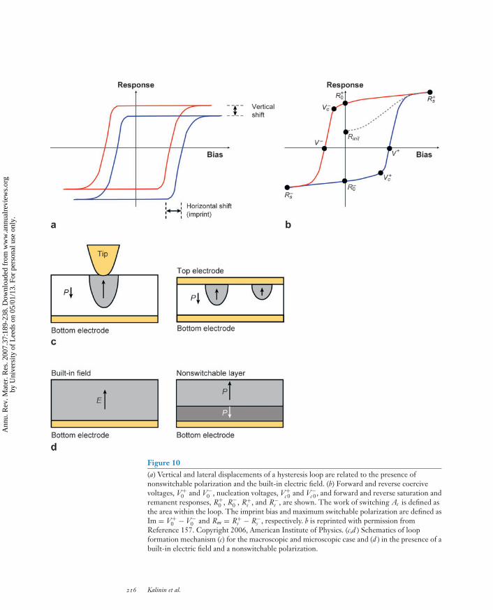
ANRV315-MR37-07 ARI 30 May 2007 21:54
Figure 10(a) Vertical and lateral displacements of a hysteresis loop are related to the presence ofnonswitchable polarization and the built-in electric field. (b) Forward and reverse coercivevoltages, V+
0 and V−0 , nucleation voltages, V+
c 0 and V−c 0, and forward and reverse saturation and
remanent responses, R+0 , R−
0 , R+s , and R−
s , are shown. The work of switching As is defined asthe area within the loop. The imprint bias and maximum switchable polarization are defined asIm = V+
0 − V−0 and Rm = R+
s − R−s , respectively. b is reprinted with permission from
Reference 157. Copyright 2006, American Institute of Physics. (c,d ) Schematics of loopformation mechanism (c) for the macroscopic and microscopic case and (d ) in the presence of abuilt-in electric field and a nonswitchable polarization.
216 Kalinin et al.
Ann
u. R
ev. M
ater
. Res
. 200
7.37
:189
-238
. Dow
nloa
ded
from
ww
w.a
nnua
lrev
iew
s.or
gby
Uni
vers
ity o
f L
eeds
on
05/0
1/13
. For
per
sona
l use
onl
y.
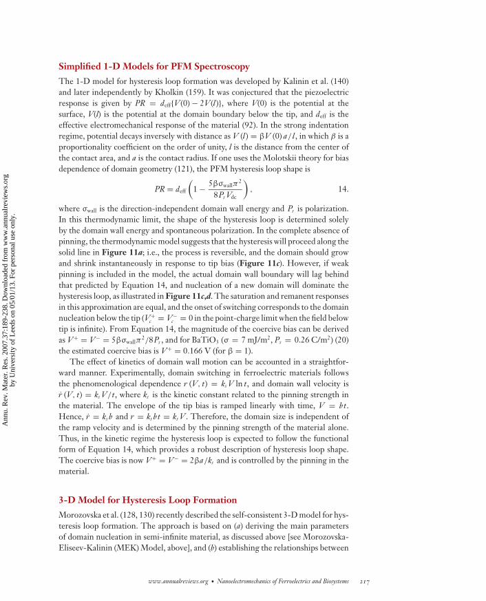
ANRV315-MR37-07 ARI 30 May 2007 21:54
Simplified 1-D Models for PFM Spectroscopy
The 1-D model for hysteresis loop formation was developed by Kalinin et al. (140)and later independently by Kholkin (159). It was conjectured that the piezoelectricresponse is given by PR = deff{V(0) − 2V(l)}, where V(0) is the potential at thesurface, V(l) is the potential at the domain boundary below the tip, and deff is theeffective electromechanical response of the material (92). In the strong indentationregime, potential decays inversely with distance as V (l) = βV (0) a/ l , in which β is aproportionality coefficient on the order of unity, l is the distance from the center ofthe contact area, and a is the contact radius. If one uses the Molotskii theory for biasdependence of domain geometry (121), the PFM hysteresis loop shape is
PR = deff
(1 − 5βσwallπ
2
8Ps Vdc
), 14.
where σwall is the direction-independent domain wall energy and Ps is polarization.In this thermodynamic limit, the shape of the hysteresis loop is determined solelyby the domain wall energy and spontaneous polarization. In the complete absence ofpinning, the thermodynamic model suggests that the hysteresis will proceed along thesolid line in Figure 11a; i.e., the process is reversible, and the domain should growand shrink instantaneously in response to tip bias (Figure 11c). However, if weakpinning is included in the model, the actual domain wall boundary will lag behindthat predicted by Equation 14, and nucleation of a new domain will dominate thehysteresis loop, as illustrated in Figure 11c,d. The saturation and remanent responsesin this approximation are equal, and the onset of switching corresponds to the domainnucleation below the tip (V+
c = V−c = 0 in the point-charge limit when the field below
tip is infinite). From Equation 14, the magnitude of the coercive bias can be derivedas V+ = V− = 5βσwallπ
2/8Ps , and for BaTiO3 (σ = 7 mJ/m2, Ps = 0.26 C/m2) (20)the estimated coercive bias is V+ = 0.166 V (for β = 1).
The effect of kinetics of domain wall motion can be accounted in a straightfor-ward manner. Experimentally, domain switching in ferroelectric materials followsthe phenomenological dependence r (V, t) = ks V ln t, and domain wall velocity isr (V, t) = ks V/t, where ks is the kinetic constant related to the pinning strength inthe material. The envelope of the tip bias is ramped linearly with time, V = bt.Hence, r = ks b and r = ks bt = ks V . Therefore, the domain size is independent ofthe ramp velocity and is determined by the pinning strength of the material alone.Thus, in the kinetic regime the hysteresis loop is expected to follow the functionalform of Equation 14, which provides a robust description of hysteresis loop shape.The coercive bias is now V+ = V− = 2βa/ks and is controlled by the pinning in thematerial.
3-D Model for Hysteresis Loop Formation
Morozovska et al. (128, 130) recently described the self-consistent 3-D model for hys-teresis loop formation. The approach is based on (a) deriving the main parametersof domain nucleation in semi-infinite material, as discussed above [see Morozovska-Eliseev-Kalinin (MEK) Model, above], and (b) establishing the relationships between
www.annualreviews.org • Nanoelectromechanics of Ferroelectrics and Biosystems 217
Ann
u. R
ev. M
ater
. Res
. 200
7.37
:189
-238
. Dow
nloa
ded
from
ww
w.a
nnua
lrev
iew
s.or
gby
Uni
vers
ity o
f L
eeds
on
05/0
1/13
. For
per
sona
l use
onl
y.

ANRV315-MR37-07 ARI 30 May 2007 21:54
Figure 11(a) Electromechanical hysteresis loop in the no pinning (solid line) and weak pinning (dottedline) limits. (b) Hysteresis loop (solid line) in the thermodynamic and kinetic (dotted line) limits.Forward and reverse coercive voltages, V+
0 and V−0 , nucleation voltages, V+
c 0 and V−c 0, and
forward and reverse saturation and remanent responses, R+0 , R−
0 , R+s , and R−
s , are shown. Thework of switching As is defined as the area within the loop. The imprint bias and maximumswitchable polarization are defined as Im = V+
0 − V−0 and Rm = R+
s − R−s , respectively.
Schematic representation of domain growth for the thermodynamic model (c) without pinningand (d ) with pinning. The numbers correspond to points on the hysteresis curve in a. Arrowsindicate domain orientation. Reprinted with permission from Reference 158. Copyright 2006,American Institute of Physics.
domain parameters r and l and piezoresponse signal, using decoupled Green’s func-tion theory (124, 126–128). For an interpretation of experimental data on realisticmaterials, the third step is (c) calibration of the probe geometry, using the appropriatestandard (e.g., domain wall width).
This analysis has shown that the electromechanical response in the center ofcylindrical domain has the form
218 Kalinin et al.
Ann
u. R
ev. M
ater
. Res
. 200
7.37
:189
-238
. Dow
nloa
ded
from
ww
w.a
nnua
lrev
iew
s.or
gby
Uni
vers
ity o
f L
eeds
on
05/0
1/13
. For
per
sona
l use
onl
y.
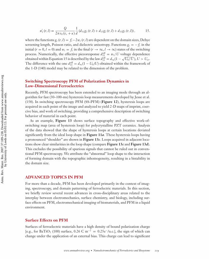
ANRV315-MR37-07 ARI 30 May 2007 21:54
ui3 (r, l) = Q
2πε0 (εe + κ)1d
(d31g1 (r, l) + d15g2 (r, l) + d33g3 (r, l)) , 15.
where the functions gi (r, l) = fi −2wi (r, l) are dependent on the domain sizes, Debyescreening length, Poisson ratio, and dielectric anisotropy. Functions gi = − fi in theinitial (r = 0, l = 0) and wi = fi in the final (r → ∞, l → ∞) states of the switchingprocess. Numerically, the effective piezoresponse d eff
33 = u3/U voltage dependenceobtained within Equation 15 is described by the law d eff
33 = d∞(1 − √U0/U ), U > Ucr.
The difference with the one d eff33 = d∞(1 − U0/U) obtained within the framework of
the 1-D (140) model may be related to the dimension of the problem.
Switching Spectroscopy PFM of Polarization Dynamics inLow-Dimensional Ferroelectrics
Recently, PFM spectroscopy has been extended to an imaging mode through an al-gorithm for fast (30–100-ms) hysteresis loop measurements developed by Jesse et al.(158). In switching spectroscopy PFM (SS-PFM) (Figure 12), hysteresis loops areacquired in each point of the image and analyzed to yield 2-D maps of imprint, coer-cive bias, and work of switching, providing a comprehensive description of switchingbehavior of material in each point.
As an example, Figure 13 shows surface topography and effective work-of-switching map (area of hysteresis loop) for polycrystalline PZT ceramics. Analysisof the data showed that the shape of hysteresis loops at certain locations deviatedsignificantly from the ideal loop shape in Figure 11a. These hysteresis loops havinga pronounced “shoulder” are shown in Figure 13c. Loops acquired in adjacent loca-tions show clear similarities in the loop shape (compare Figure 13c and Figure 13d).This excludes the possibility of spurious signals that cannot be ruled out in conven-tional PFM spectroscopy. We attribute the “abnormal” loop shape to the interactionof forming domain with the topographic inhomogeneity, resulting in a bistability inthe domain size.
ADVANCED TOPICS IN PFM
For more than a decade, PFM has been developed primarily in the context of imag-ing, spectroscopy, and domain patterning of ferroelectric materials. In this section,we briefly review several recent advances in cross-disciplinary areas related to theinterplay between electromechanics, surface chemistry, and biology, including sur-face effects on PFM, electromechanical imaging of biomaterials, and PFM in a liquidenvironment.
Surface Effects on PFM
Surfaces of ferroelectric materials have a high density of bound polarization charge[e.g., for BaTiO3 (100) surface, 0.26 C m−2 = 0.25e−/u.c.], the sign of which canchange under the application of an external bias. This charge can lead to significant
www.annualreviews.org • Nanoelectromechanics of Ferroelectrics and Biosystems 219
Ann
u. R
ev. M
ater
. Res
. 200
7.37
:189
-238
. Dow
nloa
ded
from
ww
w.a
nnua
lrev
iew
s.or
gby
Uni
vers
ity o
f L
eeds
on
05/0
1/13
. For
per
sona
l use
onl
y.

ANRV315-MR37-07 ARI 30 May 2007 21:54
–2.0–40 40200–20
–1.5
–1.0
–0.5
0.0
0.5
1.0
1.5
Resp
on
se (
a.u
.)Bias (Vdc)a
c
b
Vtip = Vdc + Vac sinωt
Highτ1 τ2
Low
Time
Am
plitu
de
τ3δτ
Figure 12(a) In switching spectroscopy PFM (SS-PFM), a local hysteresis loop is collected at each pointon N × M mesh. (b) Evolution of a PFM hysteresis loop on epitaxial PZT film with biaswindow. (c) The single-point probing waveform in SS-PFM and data acquisition sequence.Reprinted with permission from Reference 157. Copyright 2006, American Institute ofPhysics.
surface reactivity and surface chemistry effects, as has been known for nearly half acentury (160–162). The role of adsorbates on the PFM signal has been explored as afunction of temperature in barium titanate crystals (163, 164) and also in a vacuumenvironment after heating (165). The chemical reactivity of ferroelectric surfaces hasbeen exploited with the photodeposition of metal (166) and the fabrication of complexnanostructures (83, 84). Whereas previous photodeposition experiments resulted in
220 Kalinin et al.
Ann
u. R
ev. M
ater
. Res
. 200
7.37
:189
-238
. Dow
nloa
ded
from
ww
w.a
nnua
lrev
iew
s.or
gby
Uni
vers
ity o
f L
eeds
on
05/0
1/13
. For
per
sona
l use
onl
y.

ANRV315-MR37-07 ARI 30 May 2007 21:54
Figure 13Topography and SS-PFM images of polycrystalline PZT. (a) Topography (vertical scale is50 nm). (b) A map of the work of switching (area within the hysteresis loop) of approximatelythe same location as in a. (c,d ) Hysteresis loops measured at the locations indicated in b.Reprinted with permission from Reference 157. Copyright 2006, American Institute ofPhysics.
UHV: ultrahigh vacuum
metal deposition on positive domains, recently metal nanowires have been formedalong the lithium niobate domain walls via photodeposition (167).
Although surface reactivity is likely to strongly affect the electromechanical activityof ferroelectric surfaces in ambient conditions, of great interest are intrinsic surfaceeffects, including surface reconstructions and antiferrodistortive phase transitions(168), that can be studied on in-situ-grown ferroelectrics in ultrahigh vacuum (UHV).
www.annualreviews.org • Nanoelectromechanics of Ferroelectrics and Biosystems 221
Ann
u. R
ev. M
ater
. Res
. 200
7.37
:189
-238
. Dow
nloa
ded
from
ww
w.a
nnua
lrev
iew
s.or
gby
Uni
vers
ity o
f L
eeds
on
05/0
1/13
. For
per
sona
l use
onl
y.

ANRV315-MR37-07 ARI 30 May 2007 21:54
PFM of Biomaterials
As discussed in the introduction, many biological materials are piezoelectric owingto the combination of polar bonding and optical activity inherent in all biopolymers.To understand biopiezoelectricity on the nanoscale and to relate it to biological func-tionality and other materials properties, a nanoscale probe of local piezoelectricityis needed. PFM has been used for high-resolution imaging of biological structures,including human teeth, canine femoral cartilage, deer antlers, and butterfly wingscales (88, 169). PFM allows organic and mineral components of biological systemsto be differentiated and provides information on materials microstructure and localproperties (89). The use of vector PFM may also enable protein orientation to bedetermined in real space. Figure 14 shows the internal structure and orientation ofprotein microfibrils, with a spatial resolution of several nanometers in human toothenamel (170). A similar approach has been used to study electromechnical activityin dentin, cartilage, and butterfly Vanessa virginiensis wings, effectively reproducingGalvani’s experiment on the nanoscale (88, 169, 171).
PFM in a Liquid Environment
Future work in the area of relating bio-PFM to biofunctionality necessitates elec-tromechanical imaging in a liquid environment. In addition, liquid imaging elim-inates capillary forces and may be beneficial to imaging of ferroelectric materialsas well. Recently, PFM of a ferroelectric sample in a liquid environment demon-strated that both long-range electrostatic forces and capillary interactions were min-imized in liquid, resulting in a localization of the AC field to the tip-surface junc-tion and allowing 3-nm resolution to be achieved in some cases (172). Imaging atfrequencies corresponding to high-order cantilever resonances minimized the vis-cous damping, added mass effects on cantilever dynamics, and allowed sensitivitiescomparable to those of ambient conditions. A path to further improvements in res-olution to the nanometer level and below by controlling hydrophobic interactions ispredicted.
The ability to image in solution with improved sensitivity and resolution makesPFM a technique of significant value to the wide bioresearch community by allow-ing a full range of electrical and electromechanical scanning probe techniques to beemployed for the investigation of, e.g., piezoelectricity in biopolymers, molecular ori-entation, and flexoelectricity in cellular membranes. Liquid PFM may provide novelopportunities for high-resolution studies of ferroelectric materials, imaging of softelectroactive polymer materials, and imaging of biological systems in physiologicalenvironments on nanometer and ultimately molecular levels.
FUTURE DIRECTIONS IN PFM
In the decade and a half since its invention, PFM has evolved from a relatively ob-scure technique for domain imaging to a broadly accepted tool for nanoscale char-acterization, domain patterning, and spectroscopy of ferroelectric materials. PFM is
222 Kalinin et al.
Ann
u. R
ev. M
ater
. Res
. 200
7.37
:189
-238
. Dow
nloa
ded
from
ww
w.a
nnua
lrev
iew
s.or
gby
Uni
vers
ity o
f L
eeds
on
05/0
1/13
. For
per
sona
l use
onl
y.

ANRV315-MR37-07 ARI 30 May 2007 21:54
Figure 14Electromechanical imaging of tooth enamel. (a) Electromechanical response of the surface tothe tip bias is a vector measure, components of which are related to the local orientation ofprotein molecules. In PFM, detection of vertical (VPFM) and torsional (LPFM) componentsof cantilever response allows two vector components, in plane and out of plane, to besimultaneously measured. (b) Surface topography (vertical scale 20 nm) and (c) elasticity mapof 400 × 400 nm2 region on enamel surface (vertical scale is 6% of the average signal).(d ) VPFM and (e) LPFM images of the same region as a and b with a modulation bias of 10Vpp applied to the tip. The vertical scale for d is −7.5 pm V−1 to 7.5 pm V−1 (the vertical scalefor e is not calibrated). ( f ) Vector PFM map of local electromechanical response (maximum is7.5 pm V−1). Color indicates the orientation of the electromechanical response vector, whereasthe intensity provides the magnitude (color wheel diagram). (g,h) Semiquantitative maps oflocal molecular orientation. Reprinted from Reference 170 with permission from Elsevier.
www.annualreviews.org • Nanoelectromechanics of Ferroelectrics and Biosystems 223
Ann
u. R
ev. M
ater
. Res
. 200
7.37
:189
-238
. Dow
nloa
ded
from
ww
w.a
nnua
lrev
iew
s.or
gby
Uni
vers
ity o
f L
eeds
on
05/0
1/13
. For
per
sona
l use
onl
y.
ANRV315-MR37-07 ARI 30 May 2007 21:54
applicable to imaging of other piezoelectric functional materials such as III-V nitrides,providing information on crystal polarity. The recently demonstrated potential ofPFM for sub-10-nm imaging of electromechanically active proteins in calcified andconnective tissues (88, 89, 169, 170) suggests much broader applications in the bio-logical community, in which the techniques for studying the ultrastructure of tissueson the submicron level are scarce. Moreover, the pronounced difference in signalformation mechanism between PFM and force- and current-based SPMs suggeststhat there is a tremendous potential for further development. In this section, wesummarize some of the unresolved challenges and opportunities in PFM.
Probe Development
Further progress of PFM necessitates the development of probes that (a) are stableand form reliable contact with the surface, (b) have electrostatic shielding (173, 174)to minimize electrostatic force and allow reliable imaging in conductive liquid envi-ronments, and (c) have multiple electrodes to create an in-plane field with controllablestructure.
Instrumentation
The difference in PFM image formation mechanisms compared with those of AFMand STM imposes certain requirements on the SPM platform. In particular, PFMrequires the detection of small (∼picometer-scale) probe displacements in response tolarge (∼10 Vpp) periodic biases. This requires special attention to the shielding of themicroscope cabling to prevent cross talk between the driving and the detected signals.In particular, until recently most commercial microscopes required home-built tipholders to avoid the cross talk; to a large extent the limited research on PFM in aUHV environment is related to the difficulties associated with similar modificationsfor UHV operation.
The second limitation is related to the difficulty of using standard phase-lockedloop–based frequency-tracking methods for PFM and the dependence of resonancesignal both on local damping and electromechanical activity. This limitation can beovercome through the use of a recently developed band excitation method based onnonsinusoidal excitation signals (175).
Resolution
There is no fundamental limitation on achieving subnanometer and potentiallyatomic resolution in PFM. As illustrated by the single chemical bond example above(see section on Nanoscale Probing of Electromechanical Coupling), the expectedlevel of response is well within the detection limit of modern SPM systems. The pri-mary difficulty in achieving this goal is the minimization of the electrostatic responseto the measured signal and the precise control of tip-surface contact area required toachieve molecular and atomic resolution.
224 Kalinin et al.
Ann
u. R
ev. M
ater
. Res
. 200
7.37
:189
-238
. Dow
nloa
ded
from
ww
w.a
nnua
lrev
iew
s.or
gby
Uni
vers
ity o
f L
eeds
on
05/0
1/13
. For
per
sona
l use
onl
y.

ANRV315-MR37-07 ARI 30 May 2007 21:54
3-D Probes
As discussed above, the electromechanical response of the surface is generally avector having three independent components. The beam-deflection system usedin most commercial SPMs allows only normal and lateral components of the re-sponse to be detected, necessitating imaging with sample rotation; also, longitudinaldisplacement of the surface can contribute to the vertical signal. In addition,the sensitivities of vertical and lateral PFM are generally different, necessitat-ing complex and time-consuming calibration. This limitation is a fundamentalcharacteristic of a cantilever-based force sensor, and the use of alternative con-figurations for a force sensor, e.g., recently introduced 3-D SPM (176, 177) or
Figure 15Roadmap for development of SPM probes and imaging modes. Shown is the probe evolutionfrom a simple etched STM tip (current probe) to an AFM cantilever (force and current) to3-D probes with a force-sensing integrated readout and active tip (FIRAT) and shieldedprobes. In parallel, data acquisition methods have evolved from static detection (STM andcontact AFM) to constant frequency (intermittent contact AFM, AFAM, etc.) and frequencytracking (noncontact AFM) to more complex waveforms. Images reproduced with permissionfrom References 180 and 181.
www.annualreviews.org • Nanoelectromechanics of Ferroelectrics and Biosystems 225
Ann
u. R
ev. M
ater
. Res
. 200
7.37
:189
-238
. Dow
nloa
ded
from
ww
w.a
nnua
lrev
iew
s.or
gby
Uni
vers
ity o
f L
eeds
on
05/0
1/13
. For
per
sona
l use
onl
y.
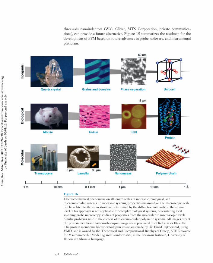
ANRV315-MR37-07 ARI 30 May 2007 21:54
three-axis nanoindentors (W.C. Oliver, MTS Corporation, private communica-tions), can provide a future alternative. Figure 15 summarizes the roadmap for thedevelopment of PFM based on future advances in probe, software, and instrumentalplatforms.
Figure 16Electromechanical phenomena on all length scales in inorganic, biological, andmacromolecular systems. In inorganic systems, properties measured on the macroscopic scalecan be related to the atom structure determined by the diffraction methods on the atomiclevel. This approach is not applicable for complex biological systems, necessitating localscanning probe microscopy studies of properties from the molecular to macroscopic levels.Similar problems arise in the context of macromolecular polymeric systems. All images exceptthe protein membrane bacteriorhodopsin image are reproduced from References 182–185.The protein membrane bacteriorhodopsin image was made by Dr. Emad Tajkhorshid, usingVMD, and is owned by the Theoretical and Computational Biophysics Group, NIH Resourcefor Macromolecular Modeling and Bioinformatics, at the Beckman Institute, University ofIllinois at Urbana-Champaign.
226 Kalinin et al.
Ann
u. R
ev. M
ater
. Res
. 200
7.37
:189
-238
. Dow
nloa
ded
from
ww
w.a
nnua
lrev
iew
s.or
gby
Uni
vers
ity o
f L
eeds
on
05/0
1/13
. For
per
sona
l use
onl
y.

ANRV315-MR37-07 ARI 30 May 2007 21:54
Theory
Although significant theoretical effort has been concentrated on understanding trans-port and elastic properties of materials on the nanoscale, much less is known aboutthe nanoscale electromechanics. Extensive effort will be required to answer questionssuch as the signal dependence on the contact area in the small contact limit, predictthe role of surface states on the signal, and model PFM in soft condensed matter andbiosystems.
PFM: BEYOND THE PIEZO- AND FERROELECTRICS
In this review, we discuss in detail electromechanical imaging of piezoelectric andferroelectric materials, domain switching, and spectroscopy on the basis of bulk mod-els for material behavior. However, with an increase in spatial resolution, SPM canbecome more and more sensitive to the surface properties of material. Further re-search (Figure 16) will yield an understanding of electromechanical coupling onthe nanometer level, establish the role of surface defects in polarization switching(Landauer paradox), and probe nanoscale polarization dynamics in phase-orderedmaterials and unusual polarization states.
In biosystems, PFM opens pathways for studies of electrophysiology on the cellularand molecular levels, such as, for example, examinations of signal propagation inneurons. Ultimately, on the molecular level, PFM can allow reactions and energytransformation pathways to be understood and become the enabling component ofmolecular electromechanical machines.
SUMMARY POINTS
1. Electromechanical coupling is ubiquitous in biological systems, inorganicmaterials, and molecular systems. The mechanical response to an appliedelectrical stimulus and the electrical response to an applied mechanical stim-ulus are the bases for numerous technological applications and accompanymany biological processes, and yet little is known about electromechanicson the nanoscale.
2. Since its invention in the early 1990s, piezoresponse force microscopy (PFM)has become the primary tool to measure local electromechanics on thenanoscale, predominantly in ferroelectric materials. The image formationmechanism in PFM is complementary to that in STM and force-based AFMin terms of signal scaling with contact area and the tensorial nature of thedetected signal. In particular, the PFM signal is independent of contact area,resulting in relative insensitivity to topographic cross talk.
3. PFM is based on a nanoscale conducting probe at the end of a cantileverthat is brought into contact with a sample surface and used to apply a biasand to measure the resulting surface deformation. Both the magnitude andsign of the displacement can be mapped out to generate images of localpiezoresponse and polarization orientation.
www.annualreviews.org • Nanoelectromechanics of Ferroelectrics and Biosystems 227
Ann
u. R
ev. M
ater
. Res
. 200
7.37
:189
-238
. Dow
nloa
ded
from
ww
w.a
nnua
lrev
iew
s.or
gby
Uni
vers
ity o
f L
eeds
on
05/0
1/13
. For
per
sona
l use
onl
y.
ANRV315-MR37-07 ARI 30 May 2007 21:54
4. PFM has evolved during the past decade and now includes several variations,including lateral PFM to measure the in-plane component of polarization,vector PFM to reconstruct the real-space polarization vector from verticaland lateral PFM images, and PFM spectroscopy to measure local electrome-chanics as a function of applied bias.
5. PFM spectroscopy has been used to generate local hysteresis loops in ferro-electric materials. From these hysteresis loops, information such as imprintand the onset of nucleation can be obtained. This information is impor-tant for any technological application based on ferroelectric switching (e.g.,FeRAM) and is required for inquiries into the fundamental mechanisms ofpolarization reversal. Recently, PFM spectroscopy was extended to an imag-ing mode. This allowed loops to be measured at every point in an image andparameters describing polarization dynamics (e.g., imprint or nucleationbias) to be extracted and represented in 2-D plots.
6. Interpretation of local hysteresis loops, although originally compared withthe formation process of macroscopic P-E loops, required the developmentof a new 3-D model based on the decoupled Green’s function theory. Thismodel allows the size of the nucleating domain during the acquisition of thehysteresis loop to be determined.
7. The universal presence of piezoelectricity in biopolymers enables applica-tions of PFM for sub-10-nm imaging of the ultrastructure of biologicalstructures such as calcified and connective tissues. Further applications ofPFM and liquid PFM for biological systems can uncover fundamental mech-anisms of flexoelectricity in cellular membranes, electromotive proteins, ionchannels, etc.
8. The achievement of molecular and ultimately atomic resolution in PFM,although theoretically possible, will require advances in AFM instrumenta-tion, data acquisition and operation modes, probe design, and theory.
ACKNOWLEDGMENTS
Research sponsored by the Division of Materials Sciences and Engineering, Officeof Basic Energy Sciences, U.S. Department of Energy, under Contract DE-AC05-00OR22725 with Oak Ridge National Laboratory, managed and operated by UT-Battelle, LLC.
LITERATURE CITED
1. Waser R, ed. 2003. Nanoelectronics and Information Technology: Advanced ElectronicMaterials and Novel Devices. Darmstadt: Wiley-VCH
2. National Nanotechnology Initiative. 2006. http://www.nano.gov/
228 Kalinin et al.
Ann
u. R
ev. M
ater
. Res
. 200
7.37
:189
-238
. Dow
nloa
ded
from
ww
w.a
nnua
lrev
iew
s.or
gby
Uni
vers
ity o
f L
eeds
on
05/0
1/13
. For
per
sona
l use
onl
y.
ANRV315-MR37-07 ARI 30 May 2007 21:54
3. Chuang TJ, Anderson PM, Wu MK, Hsieh S, eds. 2006. Nanomechanics of Ma-terials and Structures. Berlin: Springer
4. Masuhara H, Kawata S, eds. 2006. Nanoplasmonics, Vol 2: From Fundamentals toApplications. Amsterdam: Elsevier
5. Kawata S, Ohtsu M, Irie M, eds. 2002. Nano-Optics. Berlin: Springer6. Lazarev PI, ed. 2004. Molecular Electronics. Berlin: Springer7. Galvani L. 1791. Commentary on the Effect of Electricity on Muscular Motion. Transl.
RM Green, 1953, Cambridge, MA (from Latin)8. Lines ME, Glass AM. 1977. Principles and Applications of Ferroelectric and Related
Materials. Oxford, UK: Clarendon Press9. Cleland AN. 2003. Foundations of Nanomechanics: From Solid State Theory to Device
Applications. Berlin: Springer10. Newnham RE. 2005. Properties of Materials: Anisotropy, Symmetry, Structure.
New York: Oxford Univ. Press11. Hench LL, West JK. 1990. Principles of Electronic Ceramics. New York: Wiley12. Setter N, Colla EL. 1993. Ferroelectric Ceramics. Basel: Birkhauser Verlag13. Polla DL, Francis LF. 1998. Processing and characterization of piezoelec-
tric materials and integration into microelectromechanical systems. Annu. Rev.Mater. Sci. 28:563–97
14. Dabbs DM, Aksay IA. 2000. Self-assembled ceramics produced by complex-fluid templation. Annu. Rev. Phys. Chem. 51:601–22
15. Schonholzer UP, Gauckler LJ. 1999. Ceramic parts patterned in the micrometerrange. Adv. Mater. 11:630–32
16. Palkar VR, Purandare SC, Pinto R. 1999. Ferroelectric thin films of PbTiO3
on silicon. J. Phys. D 32:R1–1817. Suzuki M. 1995. Review on future ferroelectric nonvolatile memory—
FERAM—from the point-of-view of epitaxial oxide thin films. J. Ceram. Soc.Jpn. 103:1099–111
18. Scott J. 2000. Ferroelectric Memories. Berlin: Springer Verlag19. Hong S, Park N. 2007. Resistive probe storage: read/write mechanism. In Scan-
ning Probe Microscopy: Electrical and Electromechanical Phenomena on the Nanoscale,ed. SV Kalinin, A Gruverman, in press. New York: Springer
20. Jona F, Shirane G. 1993. Ferroelectric Crystals. New York: Dover Publications21. Tsymbal EY, Kohlstedt H. 2006. Tunneling across a ferroelectric. Science
313:181–8322. Cross IE. 1987. Relaxor ferroelectrics. Ferroelectrics 76:241–6723. Samara SA. 2003. The relaxation properties of compositionally disordered
ABO3 perovskites. J. Phys. Condens. Matter 15:R367–41124. Kutnjak Z, Petzelt J, Blinc R. 2006. The giant electromechanical response in
ferroelectric relaxors as a critical phenomenon. Nature 441:956–5925. Landauer R. 1957. Electrostatic considerations in BaTiO3 domain formation
during polarization reversal. J. Appl. Phys. 28:227–3426. Bratkovsky AM, Levanyuk AP. 2000. Easy collective polarization switching in
ferroelectrics. Phys. Rev. Lett. 85:4614–1727. Molotskii M, Kris R, Rosenman G. 2000. Fluctuon effects in ferroelectric po-
larization switching. J. Appl. Phys. 88:5318–27
www.annualreviews.org • Nanoelectromechanics of Ferroelectrics and Biosystems 229
Ann
u. R
ev. M
ater
. Res
. 200
7.37
:189
-238
. Dow
nloa
ded
from
ww
w.a
nnua
lrev
iew
s.or
gby
Uni
vers
ity o
f L
eeds
on
05/0
1/13
. For
per
sona
l use
onl
y.

ANRV315-MR37-07 ARI 30 May 2007 21:54
28. Gerra G, Tagantsev AK, Setter N. 2005. Surface-stimulated nucleation of re-verse domains in ferroelectrics. Phys. Rev. Lett. 94:107602
29. Scott JF. 2006. Nanoferroelectrics: statics and dynamics. J. Phys. Condens. Matter18:R361–86
30. Luo Y, Szafraniak I, Zakharov ND, Nagarajan V, Steinhart M, et al. 2003.Nanoshell tubes of ferroelectric lead zirconate titanate and barium titanate.Appl. Phys. Lett. 83:440–42
31. Urban JJ, Spanier JE, Lian OY, Yun WS, Park H. 2003. Single-crystallinebarium titanate nanowires. Adv. Mater. 15:423–26
32. Naumov II, Bellaiche L, Fu HX. 2004. Unusual phase transitions in ferroelectricnanodisks and nanorods. Nature 432:737–40
33. Ederer C, Spaldin NA. 2004. Magnetoelectrics: a new route to magnetic ferro-electrics. Nat. Mater. 3:849–51
34. Lottermoser L, Lonkai T, Amann U, Hohlwein D, Ihringer J, Fiebig M. 2004.Magnetic phase control by an electric field. Nature 430:541–44
35. Multiferroicself-assembly fabricationholds promise for furtherdevice applicationsutilizing the couplingbetween polarization,magnetization, and strainorder parameters.
35. Zheng H, Wang J, Lofland SE, Ma Z, Mohaddes-Ardabili L, et al. 2004.Multiferroic BaTiO3-CoFe2O4 nanostructures. Science 303:661–63
36. Szafraniak I, Harnagea C, Scholz R, Bhattacharyya S, Hesse D, Alexe M. 2003.Ferroelectric epitaxial nanocrystals obtained by a self-patterning method. Appl.Phys. Lett. 83:2211–23
37. Lee SK, Lee W, Alexe M, Nielsch K, Hesse D, Gosele U. 2005. Well-orderedlarge-area arrays of epitaxial ferroelectric (Bi,La)4Ti3O12 nanostructures fabri-cated by gold nanotube-membrane lithography. Appl. Phys. Lett. 86:152906
38. Alexe M, Harnagea C, Hesse D, Gosele U. 1999. Patterning and switching ofnanosize ferroelectric memory cells. Appl. Phys. Lett. 75:1793–95
39. Alexe M, Gruverman A, Harnagea C, Zakharov ND, Pignolet A, et al. 1999.Switching properties of self-assembled ferroelectric memory cells. Appl. Phys.Lett. 75:1158–60
40. Alexe M, Scott JF, Curran C, Zakharov ND, Hesse D, Pignolet A. 1998. Self-patterning nano-electrodes on ferroelectric thin films for gigabit memory ap-plications. Appl. Phys. Lett. 73:1592–94
41. Tagantsev AK. 1986. Piezoelectricity and flexoelectricity in crystalline di-electrics. Phys. Rev. B 34:5883–89
42. Petrov AG. 2002. Flexoelectricity of model and living membranes. Biochim.Biophys. Acta 1561:1–25
43. Ohta T. 2003. Processes and key properties of pool materials for “bubble fu-sion”? Int. J. Hydrog. Energy 28:1273–78
44. Fukada E, Yasuda I. 1957. On the piezoelectric effect of bone. J. Phys. Soc. Jpn.12:1158–62
45. Yasuda L. 1957. On the piezoelectric activity of bone. J. Jpn. Orthop. Surg. Soc.28:267
46. Lang SB. 1966. Pyroelectric effect in bone and tendon. Nature 212:704–547. Anderson JC, Eriksson C. 1970. Piezoelectric properties of dry and wet bone.
Nature 227:491–9248. Marino AA, Gross BD. 1989. Piezoelectricity in cementum, dentine and bone.
Archs. Oral Biol. 34:507–9
230 Kalinin et al.
Ann
u. R
ev. M
ater
. Res
. 200
7.37
:189
-238
. Dow
nloa
ded
from
ww
w.a
nnua
lrev
iew
s.or
gby
Uni
vers
ity o
f L
eeds
on
05/0
1/13
. For
per
sona
l use
onl
y.

ANRV315-MR37-07 ARI 30 May 2007 21:54
49. Fukada E. 1955. Piezoelectricity of wood. J. Phys. Jpn. 10:14950. Bazhenov VA. 1961. Piezoelectric Properties of Wood. New York: Consultants Bu-
reau51. Fukada E. 1995. Piezoelectricity of biopolymers. Biorheology 32:593–60952. Bassett CAL. 1968. Biologic significance of piezoelectricity. Calc. Tiss. Res.
1:252–7253. Marino AA, Becker RO. 1970. Piezoelectric effect and growth control in bone.
Nature 228:473–7454. Smith JW. 1968. Molecular pattern in native collagen. Nature 219:157–
5855. Reinish GB, Nowick AS. 1975. Piezoelectric properties of bone as functions of
moisture content. Nature 253:626–2756. Marino AA, Becker RO. 1975. Piezoelectricity in hydrated frozen bone and
tendon. Nature 253:627–2857. Athenstadt H. 1970. Permanent longitudinal electric polarization and pyroelec-
tric behaviour of collagenous structures and nervous tissue in man and othervertebrates. Nature 228:830–34
58. Anderson JC, Eriksson C. 1968. Electrical properties of wet collagen. Nature218:166–68
59. Lang SB. 1969. Elastic coefficients of animal bone. Science 165:287–8860. Morris RW, Kittleman LR. 1967. Piezoelectric property of otoliths. Science
158:368–7061. Andrew C, Bassett L, Pawluk RJ. 1972. Electrical behavior of cartilage during
loading. Science 178:982–8362. Weiner S, Wagner HD. 1998. The material bone: structure mechanical function
relations. Annu. Rev. Mater. Sci. 28:271–9863. Plonsey R, Barr RC. 2000. Bioelectricity: A Quantitative Approach. New York:
Kluwer64. Raphael RM, Popel AS, Brownell WE. 2000. A membrane bending model of
outer hair cell electromotility. Biophys. J. 78:2844–6265. Liberman MC, Gao J, He DZZ, Wu X, Jia S, Zuo J. 2002. Prestin is required
for electromotility of the outer hair cell and for the cochlear amplifier. Nature419:300–4
66. Balzani V, Credi A, Raymo FM, Stoddart JF. 2000. Artificial molecular ma-chines. Angew. Chem. Int. Ed. 39:3348–91
67. The pioneering workintroducing the conceptof electromechanicaldetection in SPM.
67. Gunther P, Dransfeld K. 1992. Local poling of ferroelectric polymers byscanning force microscopy. Appl. Phys. Lett. 61:1137–39
68. Franke K, Besold J, Haessler W, Seegebarth C. 1994. Modification and detec-tion of domains on ferroelectric PZT films by scanning force microscopy. Surf.Sci. Lett. 302:L283–88
69. Gruverman A, Auciello O, Tokumoto H. 1996. Scanning force microscopy forthe study of domain structure in ferroelectric thin films. J. Vac. Sci. Technol. B14:602–5
70. Gruverman A, Auciello O, Tokumoto H. 1996. Nanoscale investigation of fa-tigue effects in Pb(Zr,Ti)O3 films. Appl. Phys. Lett. 69:3191–93
www.annualreviews.org • Nanoelectromechanics of Ferroelectrics and Biosystems 231
Ann
u. R
ev. M
ater
. Res
. 200
7.37
:189
-238
. Dow
nloa
ded
from
ww
w.a
nnua
lrev
iew
s.or
gby
Uni
vers
ity o
f L
eeds
on
05/0
1/13
. For
per
sona
l use
onl
y.

ANRV315-MR37-07 ARI 30 May 2007 21:54
71. One of the firstdemonstrations of PFMon inorganic ferroelectricmaterials andferroelectric domainwriting in inorganicferroelectric thin films.
71. Hidaka T, Maruyama T, Saitoh M, Mikoshiba N, Shimizu M, et al. 1996.Formation and observation of 50 nm polarized domains in PbZr1−xTixO3
thin film using scanning probe microscope. Appl. Phys. Lett. 68:2358–59
72. Introduced theconcept of lateral PFMand demonstrated thecomplete reconstructionof surface crystallographyfrom three components ofthe electromechanicalresponse vector.
72. Eng LM, Guntherodt HJ, Schneider GA, Kopke U, Munoz Saldana J.1999. Nanoscale reconstruction of surface crystallography from three-dimensional polarization distribution in ferroelectric barium–titanate ce-ramics. Appl. Phys. Lett. 74:233–35
73. Kalinin SV, Rodriguez BJ, Jesse S, Shin S, Baddorf AP, et al. 2006. Vectorpiezoresponse force microscopy. Microsc. Microanal. 12:206–20
74. Verdaguer A, Sacha GM, Bluhm H, Salmeron M. 2006. Molecular structure ofwater at interfaces: wetting at the nanometer scale. Chem. Rev. 106:1478–510
75. Sacha GM, Verdaguer A, Salmeron M. 2006. Induced water condensation andbridge formation by electric fields in atomic force microscopy. J. Phys. Chem.B 110:14870–73
76. Gruverman A, Auciello O, Tokumoto H. 1998. Imaging and control of domainstructures in ferroelectric thin films via scanning force microscopy. Annu. Rev.Mater. Sci. 28:101–23
77. Eng LM, Grafstrom S, Loppacher Ch, Schlaphof F, Trogisch S, et al. 2001.3-Dimensional electric field distribution above and below dielectric (ferroelec-tric) surfaces: nanoscale measurements and manipulation with scanning probemicroscopy. Adv. Solid State Phys. 41:287–98
78. Alexe M, Gruverman A, eds. 2004. Nanoscale Characterization of FerroelectricMaterials. Berlin: Springer
79. Hong S, ed. 2004. Nanoscale Phenomena in Ferroelectric Thin Films. Norwell, MA:Kluwer Acad.
80. Roelofs A, Bottger U, Waser R, Schlaphof F, Trogisch S, Eng LM. 2000.Differentiating 180◦ and 90◦ switching of ferroelectric domains with three-dimensional piezoresponse force microscopy. Appl. Phys. Lett. 77:3444–46
81. Shin H, Hong S, Moon J, Jeon JU. 2002. Read/write mechanisms and datastorage system using atomic force microscopy and MEMS technology. Ultra-microscopy 91:103–10
82. Laid the foundation ofusing PFM as a tool forfundamental studies ofpolarization reversalprocesses inferroelectrics.
82. Tybell T, Paruch P, Giamarchi T, Triscone JM. 2002. Domain wall creepin epitaxial ferroelectric Pb(Zr0.2Ti0.8)O33 thin films. Phys. Rev. Lett.
89:097601
83. Established a novelmethod for metalnanostructure fabrication,referred to asferroelectric lithography.
83. Kalinin SV, Bonnell DA, Alvarez T, Lei X, Hu Z, Ferris JH. 2002. Atomicpolarization and local reactivity on ferroelectric surfaces: a new routetoward complex nanostructures. Nano Lett. 2:589–93
84. Kalinin SV, Bonnell DA, Alvarez T, Lei X, Hu Z, et al. 2004. Ferroelectriclithography of multicomponent nanostructures. Adv. Mater. 16:795–99
85. Terabe K, Nakamura M, Takekawa S, Kitamura K, Higuchi S, et al. 2003.Microscale to nanoscale ferroelectric domain and surface engineering of a near-stoichiometric LiNbO3 crystal. Appl. Phys. Lett. 82:433–35
86. Rodriguez BJ, Gruverman A, Kingon AI, Nemanich RJ, Ambacher O. 2002.Piezoresponse force microscopy for polarity imaging of GaN. Appl. Phys. Lett.80:4166–68
232 Kalinin et al.
Ann
u. R
ev. M
ater
. Res
. 200
7.37
:189
-238
. Dow
nloa
ded
from
ww
w.a
nnua
lrev
iew
s.or
gby
Uni
vers
ity o
f L
eeds
on
05/0
1/13
. For
per
sona
l use
onl
y.
ANRV315-MR37-07 ARI 30 May 2007 21:54
87. Halperin C, Mutchnik S, Agronin A, Molotskii M, Urenski P, et al. 2004. Piezo-electric effect in human bones studied in nanometer scale. Nano Lett. 4:1253–56
88. Electromechanicalactivity of biologicalsystems such as calcifiedand connective tissues wasmapped with sub-10-nmresolution, demonstratingthe potential of PFM forimaging biologicalsystems.
88. Kalinin SV, Rodriguez BJ, Jesse S, Thundat T, Gruverman A. 2005. Elec-tromechanical imaging of biological systems with sub10 nm resolution.Appl. Phys. Lett. 87:053901
89. Rodriguez BJ, Kalinin SV, Shin J, Jesse S, Grichko V, et al. 2006. Electrome-chanical probing of biomaterials by scanning probe microscopy. J. Struct. Biol.153:151–59
90. Lebedev NN, Skal’skaya IP, Uflyand Ya S. 1966. Problems in Mathematical Physics.New York: Pergamon Press
91. Sharvin YV. 1965. On a possible method to study Fermi surfaces. Zh. Eksp. Teor.Fiz. 48:984–85
92. Kalinin SV, Karapetian E, Kachanov M. 2004. Nanoelectromechanics ofpiezoresponse force microscopy. Phys. Rev. B 70:184101
93. Karapetian E, Kachanov M, Kalinin SV. 2005. Nanoelectromechanics of piezo-electric indentation and applications to scanning probe microscopies of ferro-electric materials. Philos. Mag. 85:1017–51
94. Huey BD. 2004. SPM measurements of ferroelectrics at MHz frequencies.Nanoscale Phenomena in Ferroelectric Thin Films, ed. S Hong, pp. 239–62. NewYork: Kluwer
95. Giannakopoulos AE, Suresh S. 1999. Theory of indentation of piezoelectricmaterials. Acta Mater. 47:2153–64
96. Chen WQ, Ding HJ. 1999. Indentation of a transversely isotropic piezoelectrichalf-space by a rigid sphere. Acta Mech. Solida Sin. 12:114–20
97. Karapetian E, Sevostianov I, Kachanov M. 2000. Point force and point electriccharge in infinite and semi-infinite transversely isotropic piezoelectric solids.Philos. Mag. B 80:331–59
98. Ganpule CS, Nagarajan V, Li H, Ogale AS, Steinhauer DE, et al. 2000. Roleof 90◦ domains in lead zirconate titanate thin films. Appl. Phys. Lett. 77:292–94
99. Agronin A, Molotskii M, Rosenwaks Y, Strassburg E, Boag A, et al. 2005.Nanoscale piezoelectric coefficient measurements in ionic conducting ferro-electrics. J. Appl. Phys. 97:084312
100. Felten F, Schneider GA, Munoz Saldana J, Kalinin SV. 2004. Modeling andmeasurement of surface displacements in BaTiO3 bulk material in piezoresponseforce microscopy. J. Appl. Phys. 96:563–68
101. Scrymgeour DA, Gopalan V. 2005. Nanoscale piezoelectric response across asingle antiparallel ferroelectric domain wall. Phys. Rev. B 72:024103
102. Kalinin SV, Eliseev EA, Morozovska AN. 2006. Materials contrast in piezore-sponse force microscopy. Appl. Phys. Lett. 88:232904
103. Eliseev EA, Kalinin SV, Jesse S, Bravina SL, Morozovska AN. 2007. Electrome-chanical detection in scanning probe microscopy: tip models and materials con-trast. http://www.arxiv.org; cond-mat/0607543
104. Morozovska AN, Bravina SL, Eliseev EA, Kalinin SV. 2007. Resolution functiontheory in piezoresponse force microscopy: domain wall profile, spatial resolu-tion, and tip calibration. http://www.arxiv.org; cond-mat/0608289
www.annualreviews.org • Nanoelectromechanics of Ferroelectrics and Biosystems 233
Ann
u. R
ev. M
ater
. Res
. 200
7.37
:189
-238
. Dow
nloa
ded
from
ww
w.a
nnua
lrev
iew
s.or
gby
Uni
vers
ity o
f L
eeds
on
05/0
1/13
. For
per
sona
l use
onl
y.

ANRV315-MR37-07 ARI 30 May 2007 21:54
105. Kalinin SV, Jesse S, Rodriguez BJ, Shin J, Baddorf AP, et al. 2006. Spatial resolu-tion, information limit, and contrast transfer in piezoresponse force microscopy.Nanotechnology 17:3400–11
106. Jesse S, Baddorf AP, Kalinin SV. 2006. Dynamic behavior in piezoresponseforce microscopy. Nanotechnology 17:1615–28
107. Rabe U. 2006. Atomic force acoustic microscopy. In Applied Scanning ProbeMethods, Vol II, ed. B Bhushan, H Fuchs, pp. 37–90. New York: Springer
108. The 8-nm bit sizereported here rendersferroelectrics promisingmaterials for high-density(∼10 Tbit inch−2) datastorage.
108. Cho Y, Hashimoto S, Odagawa N, Tanaka K, Hiranaga Y. 2006. Nan-odomain manipulation for ultrahigh density ferroelectric data storage.Nanotechnology 17:S137–41
109. Nassau K, Levinstein HJ, Loiacono GM. 1965. The domain structure and etch-ing of ferroelectric lithium niobate. Appl. Phys. Lett. 6:228–29
110. Kholkin AL, Bdikin IK, Shvartsman VV, Orlova A, Kiselev D, et al. 2004.Local electromechanical properties of ferroelectric materials for piezoelectricapplications. Mater. Res. Soc. Symp. Proc. 839E, O7.6
111. Paruch P, Giamarchi T, Triscone JM. 2005. Domain wall roughness in epitaxialferroelectric PbZr0.2Ti0.8O3 thin films. Phys. Rev. Lett. 94:197601
112. Dawber M, Gruverman A, Scott JF. 2006. Skyrmion model of nano-domainnucleation in ferroelectrics and ferromagnets. J. Phys. Condens. Matter 18:L71–79
113. Agronin A, Rosenwaks Y, Rosenman G. 2006. Direct observation of pinningcenters in ferroelectrics. Appl. Phys. Lett. 88:072911
114. Woo J, Hong S, Setter N, Shin H, Jeon JU, et al. 2001. Quantitative analysisof the bit size dependence on the pulse width and pulse voltage in ferroelectricmemory devices using atomic force microscopy. J. Vac. Sci. Technol. B 19:818–24
115. Rodriguez BJ, Nemanich RJ, Kingon A, Gruverman A, Kalinin SV, et al. 2005.Domain growth kinetics in lithium niobate single crystals studied by piezore-sponse force microscopy. Appl. Phys. Lett. 86:012906
116. Molotskii MI, Shvebelman MM. 2005. Dynamics of ferroelectric domain for-mation in an atomic force microscope. Philos. Mag. 85:1637–55
117. Abplanalp M. 2001. Piezoresponse scanning force microscopy of ferroelectric domains.PhD thesis. Swiss Fed. Inst. Technol., Zurich
118. Agronin A, Molotskii M, Rosenwaks Y, Rosenman G, Rodriguez BJ, et al. 2006.Dynamics of ferroelectric domain growth in the field of atomic force micro-scope. J. Appl. Phys. 99:104102
119. Gruverman A, Rodriguez BJ, Dehoff C, Waldrep JD, Kingon AI, et al. 2005. Di-rect studies of domain switching dynamics in thin film ferroelectric capacitors.Appl. Phys. Lett. 87:082902
120. Gruverman A, Kholkin A. 2006. Nanoscale ferroelectrics: processing, charac-terization and future trends. Rep. Prog. Phys. 69:2443–74
121. Molotskii M. 2003. Generation of ferroelectric domains in atomic force micro-scope. J. Appl. Phys. 93:6234–37
122. Elegantly analyzedferroelectric domainswitching in a PFMexperiment, extendingearly results of Landauer(25) to the point contactgeometry.
122. Molotskii M, Agronin A, Urenski P, Shvebelman M, Rosenman G, Rosen-waks Y. 2003. Ferroelectric domain breakdown. Phys. Rev. Lett. 90:107601
123. Shvebelman M. 2005. Static and dynamic properties of ferroelectric domains studiedby atomic force microscopy. PhD thesis. Tel Aviv University, Tel Aviv
234 Kalinin et al.
Ann
u. R
ev. M
ater
. Res
. 200
7.37
:189
-238
. Dow
nloa
ded
from
ww
w.a
nnua
lrev
iew
s.or
gby
Uni
vers
ity o
f L
eeds
on
05/0
1/13
. For
per
sona
l use
onl
y.

ANRV315-MR37-07 ARI 30 May 2007 21:54
124. Kalinin SV, Gruverman A, Rodriguez BJ, Shin J, Baddorf AP, et al. 2005. Nano-electromechanics of polarization switching in piezoresponse force microscopy.J. Appl. Phys. 97:074305
125. Emelyanov AY. 2005. Coherent ferroelectric switching by atomic force mi-croscopy. Phys. Rev. B 71:132102
126. Morozovska AN, Eliseev EA. 2006. Screening and size effects on the nan-odomain tailoring in ferroelectrics semiconductors. Phys. Rev. B 73:104440
127. Morozovska AN, Eliseev EA. 2006. The study of screening phenomena underthe nano-domain formation in ferroelectric semiconductors. Phys. Status SolidiB 243:1996–2011
128. Morozovska AN, Eliseev EA, Kalinin SV. 2006. Domain nucleation and hystere-sis loop shape in piezoresponse force spectroscopy. Appl. Phys. Lett. 89:192901
129. Molotskii M. 2003. Forward motion of ferroelectric domain walls. Philos. Mag.Lett. 83:763–67
130. Morozovska AN, Svechnikov SV, Eliseev EA, Jesse S, Rodriguez BJ, KalininSV. 2007. Piezoresponse force spectroscopy of ferroelectric materials. http://www.arxiv.org; cond-mat/0610764
131. Molotskii M. 2005. Generation of ferroelectric domains in films using atomicforce microscope. J. Appl. Phys. 97:014109
132. Molotskii M, Rosenwaks Y, Rosenman G. 2007. Ferroelectric domain break-down. Annu. Rev. Mater. Res. 37:271–96
133. Kalinin SV, Bonnell DA. 2000. Effect of phase transition on the surface potentialof the BaTiO3(100) surface by variable temperature scanning surface potentialmicroscopy. J. Appl. Phys. 87:3950–57
134. Kalinin SV, Johnson CY, Bonnell DA. 2002. Domain polarity and temperatureinduced potential inversion on the BaTiO3(100) surface. J. Appl. Phys. 91:3816–23
135. Kalinin SV, Bonnell DA. 2001. Local potential and polarization screening onferroelectric surfaces. Phys. Rev. B 63:125411
136. Buhlmann S, Colla E, Muralt P. 2005. Polarization reversal due to charge in-jection in ferroelectric films. Phys. Rev. B 72:214120
137. Birk H, Glatz-Reichenbach J, Li-Jie Schreck E, Dransfeld K. 1991. The lo-cal piezoelectric activity of thin polymer films observed by scanning tunnelingmicroscopy. J. Vac. Sci. Technol. B 9:1162–65
138. Guo HY, Xu JB, Wilson IH, Xie Z, Luo EZ, et al. 2002. Study of domainstability on (Pb0.76Ca0.24)TiO3 thin films using piezoresponse microscopy. Appl.Phys. Lett. 81:715–17
139. Kim ID, Avrahami Y, Tuller HL, Park YB, Dicken MJ, Atwater HA. 2005.Study of orientation effect on nanoscale polarization in BaTiO3 thin films usingpiezoresponse force microscopy. Appl. Phys. Lett. 86:192907
140. Kalinin SV, Gruverman A, Bonnell DA. 2004. Quantitative analysis of nanoscaleswitching in SrBi2Ta2O9 thin films by piezoresponse force microscopy. Appl.Phys. Lett. 85:795–97
141. Eng LM, Guntherodt HJ, Rosenman G, Skliar A, Oron M, et al. 1998. Nonde-structive imaging and characterization of ferroelectric domains in periodicallypoled crystals. J. Appl. Phys. 83:5973–77
www.annualreviews.org • Nanoelectromechanics of Ferroelectrics and Biosystems 235
Ann
u. R
ev. M
ater
. Res
. 200
7.37
:189
-238
. Dow
nloa
ded
from
ww
w.a
nnua
lrev
iew
s.or
gby
Uni
vers
ity o
f L
eeds
on
05/0
1/13
. For
per
sona
l use
onl
y.

ANRV315-MR37-07 ARI 30 May 2007 21:54
142. Rodriguez BJ, Gruverman A, Kingon AI, Nemanich RJ, Cross JS. 2004. Three-dimensional high-resolution reconstruction of polarization in ferroelectric ca-pacitors by piezoresponse force microscopy. J. Appl. Phys. 95:1958–62
143. Desfeux R, Legrand C, Da Costa A, Chateigner D, Bouregba R, Poullain G.2006. Correlation between local hysteresis and crystallite orientation in PZTthin films deposited on Si and MgO substrates. Surf. Sci. 600:219–28
144. Buhlmann S. 2004. Patterned and self-assembled ferroelectric nano-structures ob-tained by epitaxial growth and e-beam lithography. PhD thesis. Ecole Polytech.Fed., Lausanne, Switzerland
145. Saya Y, Watanabe S, Kawai M, Yamada H, Matsushige K. 2000. Investiga-tion of nonswitching regions in ferroelectric thin films using scanning forcemicroscopy. Jpn. J. Appl. Phys. 39:3799–803
146. Alexe M, Harnagea C, Hesse D, Gosele U. 2001. Polarization imprint and sizeeffects in mesoscopic ferroelectric structures. Appl. Phys. Lett. 79:242–44
147. Ma W, Hesse D. 2004. Polarization imprint in ordered arrays of epitaxial fer-roelectric nanostructures. Appl. Phys. Lett. 84:2871–73
148. Harnagea C, Pignolet A, Alexe M, Hesse D, Gosele U. 2000. Quantitativeferroelectric characterization of single submicron grains in bi-layered perovskitethin films. Appl. Phys. A 70:261–67
149. Ricinschi D, Mitoseriu L, Stancu A, Postolache P, Okuyama M. 2004. Anal-ysis of the switching characteristics of PZT films by first order reversal curvediagrams. Integr. Ferroelec. 67:103–15
150. Ricinschi D, Noda M, Okuyama M, Ishibashi Y, Iwata M, Mitoseriu L. 2003. ALandau-theory-based computational study of in-plane and out-of-plane polar-ization components role in switching of ferroelectric thin films. J. Korean Phys.Soc. 42:S1232–36
151. Ricinschi D, Okuyama M. 2002. Nanoscale spatial correlation of piezoelectricdisplacement hysteresis loops of PZT films in the fresh and fatigued states.Integr. Ferroelec. 50:149–58
152. Gruverman A, Rodriguez BJ, Kingon AI, Nemanich RJ, Cross JS, Tsukada M.2003. Spatial inhomogeneity of imprint and switching behavior in ferroelectriccapacitors. Appl. Phys. Lett. 82:3071–73
153. Gruverman A, Rodriguez BJ, Kingon AI, Nemanich RJ, Tagantsev AK, et al.2003. Mechanical stress effect on imprint behavior of integrated ferroelectriccapacitors. Appl. Phys. Lett. 83:728–30
154. Dehoff C, Rodriguez BJ, Kingon AI, Nemanich RJ, Gruverman A, Cross JS.2005. Atomic force microscopy-based experimental setup for studying domainswitching dynamics in ferroelectric capacitors. Rev. Sci. Instrum. 76:023708
155. Abplanalp M, Fousek J, Gunter P. 2001. Higher order ferroic switching inducedby scanning force microscopy. Phys. Rev. Lett. 86:5799–802
156. Harnagea C. 2001. Local piezoelectric response and domain structures in ferroelectricthin films investigated by voltage-modulated force microscopy. PhD thesis. Martin-Luther-Univ. Halle-Wittenberg, Halle
157. Jesse S, Lee HN, Kalinin SV. 2006. Quantitative mapping of switching behaviorin piezoresponse force microscopy. Rev. Sci. Instrum. 77:073702
236 Kalinin et al.
Ann
u. R
ev. M
ater
. Res
. 200
7.37
:189
-238
. Dow
nloa
ded
from
ww
w.a
nnua
lrev
iew
s.or
gby
Uni
vers
ity o
f L
eeds
on
05/0
1/13
. For
per
sona
l use
onl
y.

ANRV315-MR37-07 ARI 30 May 2007 21:54
158. Jesse S, Baddorf AP, Kalinin SV. 2006. Switching spectroscopy piezoresponseforce microscopy of ferroelectric materials. Appl. Phys. Lett. 88:062908
159. Wu A, Vilarinho PM, Shvartsman VV, Suchaneck G, Kholkin AL. 2005. Do-main populations in lead zirconate titanate thin films of different compositionsvia piezoresponse force microscopy. Nanotechnology 16(11):2587–95
160. Pearson GL, Feldmann WL. 1958. Powder-pattern techniques for delineatingferroelectric domain structures. J. Phys. Chem. Solids 9:28–30
161. Distler GI, Konstantinova VP, Gerasimov VM, Tolmacheva GA. 1968. Inter-action of defect and domain structures of triglycine sulphate crystals in ferro-electric and paraelectric states. Nature 218:762–65
162. Distler GI. 1968. The real structure of crystals and selective nucleation at surfacelocal long range active centres. J. Cryst. Growth 3:175–79
163. Kalinin SV, Bonnell DA. 2002. Imaging mechanism of piezoresponse forcemicroscopy of ferroelectric surfaces. Phys. Rev. B 65:125408
164. Kalinin SV, Bonnell DA. 2001. Temperature dependence of polarization andcharge dynamics on the BaTiO3(100) surface by scanning probe microscopy.Appl. Phys. Lett. 78:1116–18
165. Peter F, Szot K, Waser R, Reichenberg B, Tiedke S, Szade J. 2004. Piezore-sponse in the light of surface adsorbates: relevance of defined surface conditionsfor perovskite materials. Appl. Phys. Lett. 85:2896–98
166. Giocondi JL, Rohrer GS. 2001. Spatially selective photochemical reduction ofsilver on the surface of ferroelectric barium titanate. Chem. Mater. 13:241–42
167. Hanson JN, Rodriguez BJ, Nemanich RJ, Gruverman A. 2006. Fabricationof metallic nanowires on a ferroelectric template via photochemical reaction.Nanotechnology 17:4946–49
168. Munkholm A, Streiffer SK, Ramana Murty MV, Eastman JA, Thompson C,et al. 2002. Antiferrodistortive reconstruction of the PbTiO3(001) surface. Phys.Rev. Lett. 88:016101
169. Gruverman A, Rodriguez BJ, Kalinin SV. 2006. BioPFM. In Scanning ProbeMicroscopy: Electrical and Electromechanical Phenomena on the Nanoscale, ed. SVKalinin, A Gruverman, in press. New York: Springer Verlag
170. Kalinin SV, Rodriguez BJ, Shin J, Jesse S, Grichko V, et al. 2006. Bioelec-tromechanical imaging by scanning probe microscopy: Galvani’s experiment atthe nanoscale. Ultramicroscopy 106:334–40
171. Physics Update. 2006. Phys. Today Jan 2006:9
172. Demonstratedhigh-resolution PFMimaging in a liquidenvironment, opening thepathway toelectromechanicalprobing of biologicalsystems in physiologicalenvironments.
172. Rodriguez BJ, Jesse S, Baddorf AP, Kalinin SV. 2006. High resolutionelectromechanical imaging of ferroelectric materials in a liquid environ-ment by piezoresponse force microscopy. Phys. Rev. Lett. 96:237602
173. Stephenson K, Smith T. 2006. Electrochemical SPM: fundamentals and appli-cations. In Scanning Probe Microscopy: Electrical and Electromechanical Phenomenaon the Nanoscale, ed. SV Kalinin, A Gruverman, pp. 280–314. New York: SpringerVerlag
174. Rosner BT, van der Weide DW. 2002. High-frequency near-field microscopy.Rev. Sci. Instrum. 73:2505–25
175. Kalinin SV, Jesse S. 2006. U.S. Patent Appl. No. 11/513,348
www.annualreviews.org • Nanoelectromechanics of Ferroelectrics and Biosystems 237
Ann
u. R
ev. M
ater
. Res
. 200
7.37
:189
-238
. Dow
nloa
ded
from
ww
w.a
nnua
lrev
iew
s.or
gby
Uni
vers
ity o
f L
eeds
on
05/0
1/13
. For
per
sona
l use
onl
y.

ANRV315-MR37-07 ARI 30 May 2007 21:54
176. Onaran AG, Balantekin M, Lee W, Hughes WL, Buchine BA, et al. 2006. Anew atomic force microscope probe with force sensing integrated readout andactive tip. Rev. Sci. Instrum. 77:023501
177. Dienwiebel M, de Kuyper E, Crama L, Frenken JWM, Heimberg JA, et al. 2005.Design and performance of a high-resolution frictional force microscope withquantitative three-dimensional force sensitivity. Rev. Sci. Instrum. 76:043704
178. Morrison FD, Luo Y, Szafraniak I, Nagarajan V, Wehrspohn RB, et al. 2003.Ferroelectric nanotubes. Rev. Adv. Mater. Sci. 4:114–22
179. Rosenman G, Urenski P, Agronin A, Rosenwaks Y, Molotskii M. 2003. Sub-micron ferroelectric domain structures tailored by high-voltage scanning probemicroscopy. Appl. Phys. Lett. 82:103–5
180. Onaran AG, Balantekin M, Lee W, Hughes WL, Buchine BA, et al. 2006. Anew atomic force microscope probe with force sensing integrated readout andactive tip. Rev. Sci. Instrum. 77:023501
181. Frederix PLTM, Gullo MR, Akiyama T, Tonin A, de Rooij NF, et al. 2005.Assessment of insulated conductive cantilevers for biology and electrochemistry.Nanotechnology 16:997–1005
182. Precision Acoustics Ltd. www.acoustics.co.uk/5Transducers.jpg183. Murayama E. www.op.titech.ac.jp/lab/okui/murayam/pvdf.jpg184. Bai M, Poulsen M, Ducharme S. 2006. Effects of annealing conditions on fer-
roelectric nanomesa self-assembly. J. Phys. Condens. Matter 18:7383–92185. Qu H, Yao W, Garcia T, Zhang J, Sorokin AV, et al. 2003. Nanoscale polariza-
tion manipulation and conductance switching in ultrathin films of a ferroelectriccopolymer. Appl. Phys. Lett. 82:4322–24
238 Kalinin et al.
Ann
u. R
ev. M
ater
. Res
. 200
7.37
:189
-238
. Dow
nloa
ded
from
ww
w.a
nnua
lrev
iew
s.or
gby
Uni
vers
ity o
f L
eeds
on
05/0
1/13
. For
per
sona
l use
onl
y.

AR315-FM ARI 31 May 2007 15:12
Annual Review ofMaterials Research
Volume 37, 2007Contents
MATERIALS CHARACTERIZATION
Low-Temperature Degradation of Zirconia and Implications forBiomedical ImplantsJerome Chevalier, Laurent Gremillard, and Sylvain Deville � � � � � � � � � � � � � � � � � � � � � � � � � � � � �1
Single-Molecule Micromanipulation TechniquesK. C. Neuman, T. Lionnet, and J.-F. Allemand � � � � � � � � � � � � � � � � � � � � � � � � � � � � � � � � � � � � � � � � � 33
Spin-Polarized Scanning Tunneling Microscopy of MagneticStructures and Antiferromagnetic Thin FilmsWulf Wulfhekel and Jürgen Kirschner � � � � � � � � � � � � � � � � � � � � � � � � � � � � � � � � � � � � � � � � � � � � � � � � � � � 69
Microscale Characterization of Mechanical PropertiesK. J. Hemker and W. N. Sharpe, Jr. � � � � � � � � � � � � � � � � � � � � � � � � � � � � � � � � � � � � � � � � � � � � � � � � � � � � � 93
Three-Dimensional Atom-Probe Tomography: Advances andApplicationsDavid N. Seidman � � � � � � � � � � � � � � � � � � � � � � � � � � � � � � � � � � � � � � � � � � � � � � � � � � � � � � � � � � � � � � � � � � � � � � �127
The Study of Nanovolumes of Amorphous Materials Using ElectronScatteringDavid J. H. Cockayne � � � � � � � � � � � � � � � � � � � � � � � � � � � � � � � � � � � � � � � � � � � � � � � � � � � � � � � � � � � � � � � � � � � �159
Nanoscale Electromechanics of Ferroelectric and Biological Systems:A New Dimension in Scanning Probe MicroscopySergei V. Kalinin, Brian J. Rodriguez, Stephen Jesse, Edgar Karapetian,
Boris Mirman, Eugene A. Eliseev, and Anna N. Morozovska � � � � � � � � � � � � � � � � � � � � � � �189
AFM and Acoustics: Fast, Quantitative Nanomechanical MappingBryan D. Huey � � � � � � � � � � � � � � � � � � � � � � � � � � � � � � � � � � � � � � � � � � � � � � � � � � � � � � � � � � � � � � � � � � � � � � � � � � �351
Electron Holography: Applications to Materials QuestionsHannes Lichte, Petr Formanek, Andreas Lenk, Martin Linck,
Christopher Matzeck, Michael Lehmann, and Paul Simon � � � � � � � � � � � � � � � � � � � � � � � � � �539
Three-Dimensional Characterization of Microstructure by ElectronBack-Scatter DiffractionAnthony D. Rollett, S.-B. Lee, R. Campman, and G.S. Rohrer � � � � � � � � � � � � � � � � � � � � � � �627
vii
Ann
u. R
ev. M
ater
. Res
. 200
7.37
:189
-238
. Dow
nloa
ded
from
ww
w.a
nnua
lrev
iew
s.or
gby
Uni
vers
ity o
f L
eeds
on
05/0
1/13
. For
per
sona
l use
onl
y.
AR315-FM ARI 31 May 2007 15:12
Atom Probe Tomography of Electronic MaterialsThomas F. Kelly, David J. Larson, Keith Thompson, Roger L. Alvis,
Joseph H. Bunton, Jesse D. Olson, and Brian P. Gorman � � � � � � � � � � � � � � � � � � � � � � � � � � � �681
Electron Holography: Phase Imaging with Nanometer ResolutionMartha R. McCartney and David J. Smith � � � � � � � � � � � � � � � � � � � � � � � � � � � � � � � � � � � � � � � � � � � �729
FERROELECTRICS AND RELATED MATERIALS, David R. Clarkeand Venkatraman Gopalan, Guest Editors
Atomic-Level Simulation of Ferroelectricity in Oxides: Current Statusand OpportunitiesSimon R. Phillpot, Susan B. Sinnott, and Aravind Asthagiri � � � � � � � � � � � � � � � � � � � � � � � � �239
Ferroelectric Domain BreakdownMichel Molotskii, Yossi Rosenwaks, and Gil Rosenman � � � � � � � � � � � � � � � � � � � � � � � � � � � � � � � � �271
Local Structure of Ferroelectric MaterialsT. Egami � � � � � � � � � � � � � � � � � � � � � � � � � � � � � � � � � � � � � � � � � � � � � � � � � � � � � � � � � � � � � � � � � � � � � � � � � � � � � � � � � �297
Terahertz PolaritonicsT. Feurer, Nikolay S. Stoyanov, David W. Ward, Joshua C. Vaughan,
Eric R. Statz, and Keith A. Nelson � � � � � � � � � � � � � � � � � � � � � � � � � � � � � � � � � � � � � � � � � � � � � � � � � � � �317
Spiral Magnets as MagnetoelectricsT. Kimura � � � � � � � � � � � � � � � � � � � � � � � � � � � � � � � � � � � � � � � � � � � � � � � � � � � � � � � � � � � � � � � � � � � � � � � � � � � � � � � � �387
Universal Domain Wall Dynamics in Disordered Ferroic MaterialsW. Kleemann � � � � � � � � � � � � � � � � � � � � � � � � � � � � � � � � � � � � � � � � � � � � � � � � � � � � � � � � � � � � � � � � � � � � � � � � � � � � �415
Defect–Domain Wall Interactions in Trigonal FerroelectricsVenkatraman Gopalan, Volkmar Dierolf, and David A. Scrymgeour � � � � � � � � � � � � � � � � �449
Influence of Electric Field and Mechanical Stresses on the Fracture ofFerroelectricsGerold A. Schneider � � � � � � � � � � � � � � � � � � � � � � � � � � � � � � � � � � � � � � � � � � � � � � � � � � � � � � � � � � � � � � � � � � � � � �491
Strain Tuning of Ferroelectric Thin FilmsDarrell G. Schlom, Long-Qing Chen, Chang-Beom Eom, Karin M. Rabe,
Stephen K. Streiffer, and Jean-Marc Triscone � � � � � � � � � � � � � � � � � � � � � � � � � � � � � � � � � � � � � � � �589
Ferroelectric Epitaxial Thin Films for Integrated OpticsBruce W. Wessels � � � � � � � � � � � � � � � � � � � � � � � � � � � � � � � � � � � � � � � � � � � � � � � � � � � � � � � � � � � � � � � � � � � � � � � � � �659
Index
Cumulative Index of Contributing Authors, Volumes 33–37 � � � � � � � � � � � � � � � � � � � � � � � �769
Errata
An online log of corrections to Annual Review of Materials Research chapters (if any,1997 to the present) may be found at http://matsci.annualreviews.org/errata.shtml
viii Contents
Ann
u. R
ev. M
ater
. Res
. 200
7.37
:189
-238
. Dow
nloa
ded
from
ww
w.a
nnua
lrev
iew
s.or
gby
Uni
vers
ity o
f L
eeds
on
05/0
1/13
. For
per
sona
l use
onl
y.