Embed Size (px)
Citation preview

Nanoindentation of Si Nanostructures: Buckling and Friction atNanoscalesHuai Huang, Bin Li, Qiu Zhao, Zhiquan Luo, Jay Im et al. Citation: AIP Conf. Proc. 1143, 204 (2009); doi: 10.1063/1.3169260 View online: http://dx.doi.org/10.1063/1.3169260 View Table of Contents: http://proceedings.aip.org/dbt/dbt.jsp?KEY=APCPCS&Volume=1143&Issue=1 Published by the American Institute of Physics. Related ArticlesStatistical analysis of the low-temperature internal friction dislocation peak (Bordoni peak) in nanostructuredcopper Low Temp. Phys. 37, 625 (2011) In situ nanomechanical testing in focused ion beam and scanning electron microscopes Rev. Sci. Instrum. 82, 063901 (2011) Nanoscale rotational deformation in solids at high stresses Appl. Phys. Lett. 98, 181909 (2011) Correlation and size dependence of the lattice strain, binding energy, elastic modulus, and thermal stability forAu and Ag nanostructures J. Appl. Phys. 109, 074319 (2011) Mechanical deformation of carbon nanotube nano-rings on flat substrate J. Appl. Phys. 109, 074304 (2011) Additional information on AIP Conf. Proc.Journal Homepage: http://proceedings.aip.org/ Journal Information: http://proceedings.aip.org/about/about_the_proceedings Top downloads: http://proceedings.aip.org/dbt/most_downloaded.jsp?KEY=APCPCS Information for Authors: http://proceedings.aip.org/authors/information_for_authors
Downloaded 19 Dec 2011 to 146.6.102.108. Redistribution subject to AIP license or copyright; see http://proceedings.aip.org/about/rights_permissions
Nanoindentation of Si Nanostructures: Buckling and Friction at Nanoscales
Huai Huanga, Bin Lia, Qiu Zhaoa, Zhiquan Luoa, Jay Ima, Min K. Kangb, Richard A. Allenc, Michael W. Cresswellc, Rui Huangb and Paul S. Hoa
a Microelectronics Research Center, The University of Texas at Austin, 10100 Burnet Road, Austin, Texas 78758, USA
b Department of Aerospace Engineering and Engineering Mechanics, University of Texas, Austin, Texas 78712, USA
c Semiconductor Electronics Division, National Institute of Standards and Technology, Gaithersburg, Maryland 20899, USA
Abstract. A nanoindentation system was employed to characterize mechanical properties of silicon nanolines (SiNLs), which were fabricated by an anisotropic wet etching (AWE) process. The SiNLs had the linewidth ranging from 24 nm to 90 nm, having smooth and vertical sidewalls and the aspect ratio (height/linewidth) from 7 to 18. During indentation, a buckling instability was observed at a critical load, followed by a displacement burst without a load increase, then a full recovery of displacement upon unloading. This phenomenon was explained by two bucking modes. It was also found that the difference in friction at the contact between the indenter and SiNLs directly affected buckling response of these nanolines. The friction coefficient was estimated to be in a range of 0.02 to 0.05. For experiments with large indentation displacements, irrecoverable indentation displacements were observed due to fracture of Si nanolines, with the strain to failure estimated to be from 3.8% to 9.7%. These observations indicated that the buckling behavior of SiNLs depended on the combined effects of load, line geometry, and the friction at contact. This study demonstrated a valuable approach to fabrication of well-defined Si nanoline structures and the application of the nanoindentation method for investigation of their mechanical properties at the nanoscale.
Keywords: Silicon nanolines, Anisotropic wet etching, Nanoindentation, Buckling instability, Displacement burst PACS: 62.25.-g Mechanical properties of nanoscale
INTRODUCTION
As the scaling of device dimensions continues, fabrication of nanoscale structures and the characterization of their mechanical properties pose significant challenges for future development of ultra large-scale integrated (ULSI) circuits. In particular, silicon-based nanostructures can serve as essential building blocks for nanoelectronic devices and nano-electromechanical systems (NEMS). For example, silicon nanowires were used for resonant sensing in nanomechanical systems1, and silicon nanobeams were used as nano-gratings for high-precision optical measurement of displacement2. Silicon-based nano-structures were also employed to form nano-scale electronic field-effect-transistors(FETs)3 or ultrasensitive sensors4 for detecting biomedical species. The mechanical properties of silicon play an important role in controlling the functionality and reliability of nano-devices.
CP1143, Stress-Induced Phenomena in Metallization: l(fh International Workshop, edited by P. S. Ho, S. Ogawa, andE. Zschech C 2009 American Institute of Physics 978-0-7354-0680-3/09/S25.00
204
Downloaded 19 Dec 2011 to 146.6.102.108. Redistribution subject to AIP license or copyright; see http://proceedings.aip.org/about/rights_permissions
The effects of size on mechanical properties of materials has been a hot topic for past decades. Many experiments revealed that the materials properties change at small scale. For single-crystal silicon, Hoffmann et al. reported an increased average strain to failure of 6% and a fracture strength of 12 GPa for silicon nanowires (SiNWs) with diameters between 90 nm and 200 nm5. The measured strength was significantly higher than those for microscale Silicon beams (4 GPa)6 and millimeter scale Silicon beams ( 500 MPa)7. It has also been reported that a transition occurred in frictional shear strength, decreasing almost one order of magnitude as the contact radii shrank into the nanoscale range8. However, it is still kept unknown if this trend extends to a few tens of nanometer size range. This is mainly due to requirements of proper sample handling, transducer resolution, and the interpretation of measurement data, making characterization of mechanical properties at nanometer scale a great challenge.
In this study, a top-down fabrication process was developed to provide single-crystal, parallel, silicon nanolines (SiNLs) with atomically flat sidewalls and well defined cross sections, by combining electron-beam lithography (EBL) and anisotropic wet etching (AWE). Those SiNLs were then characterized by an atomic force microscope (AFM) based nanoindentation tests. Finite element method (FEM) simulations were used for extraction of material properties of the SiNLs, e.g. strain to failure, friction coefficient at the nano-contact, etc. Buckling instability was observed and explained by transition of buckling modes. It was found that the buckling behavior of these SiNLs was dependent on the combined effects of load, line geometry, mechanical properties of SiNLs, and the friction properties at the contact.
EXPERIMENTAL APPROACH
Fabrication of Silicon Nanolines
The SiNLs were fabricated on a (110) wafer. The details of the fabrication process were previously published9. Basically, the pattern is written in photoresist by the EBL and sequentially transferred first to a thin Cr hard mask and then to a SiO2 hard mask using reactive ion etching (RIE). The high-resolution EBL methods were capable of producing patterns with feature dimensions less than 20 nm, providing the finest pattern we can obtain from a top down approach. Finally, the patterns were transferred into the silicon by AWE. AWE is a pattern transfer method based on the large etching rate differences among different crystal orientations, which results in an atomically flat surface on the (111) sidewall on the (110) wafer when the line direction is aligned with <112> crystal direction10.
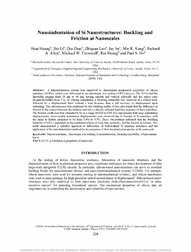
Figure 1 shows scanning electron microscope (SEM) images of the parallel SiNLs with 24 nm and 90 nm line widths. These high aspect ratio nanolines, possessing well-defined geometry with smooth sidewalls and highly uniform line widths, were well-suited for the mechanical characterization experiments. The line dimensions are summarized in Table 1. To allow for comparison of the mechanical responses of different line widths, the trench widths and aspect ratios were kept the same for the two test structures.
Nanoindentation Tests
An atomic force microscope (AFM) based nanoindentation system (a Triboscope system from Hysitron, Inc.)§ with a conically shaped indenter with the tip radius at around 3.5μm. The indentation location was set in the center area of the 30 μm by 30μm array of the SiNLs to minimize the boundary effect. A contact mode AFM scan was conducted before the indentation to make certain that the tip
§ Certain commercial equipment, instruments, or materials are identified in this document in order to specify adequate measurement procedures. Such identification does not imply recommendation or endorsement by the National Institute of Standards and Technology, nor does it imply that the materials or equipment identified are necessarily the best available for the purpose.
205
Downloaded 19 Dec 2011 to 146.6.102.108. Redistribution subject to AIP license or copyright; see http://proceedings.aip.org/about/rights_permissions
indented right in the center of the trench between two nanolines. The indentation tests were preformed in a load-controlled mode with a trapezoidally shaped loading profile. The force applied on the indenter tip increased monotonically at a constant loading rate, and then dwelt at the peak load for 1 second before it was unloaded at the same rate. The force vs. displacement was recorded continuously for both loading and unloading processes.
FIGURE 1. Cross-sectional SEM images of the two sets of high aspect ratio SiNLs. Tilt angle is 60°. (a) 24 nm wide lines (b) 90 nm wide lines. Some hillocks appear on the 24 nm SiNLs, which may due to a fast wet etching in
the fabrication process.
TABLE (1). Dimensions of the two sets of SiNLs fabricated for indentation tests. Line Dimension (nm) SiNL Set 1 SiNL Set 2
Width 24 90
Height 380 1400
Pitch 390 450
Trench Width 366 360
Aspect ratio 15.8 15.6
RESULTS & DISCUSSION
Buckling Behavior of 24nm SiNL
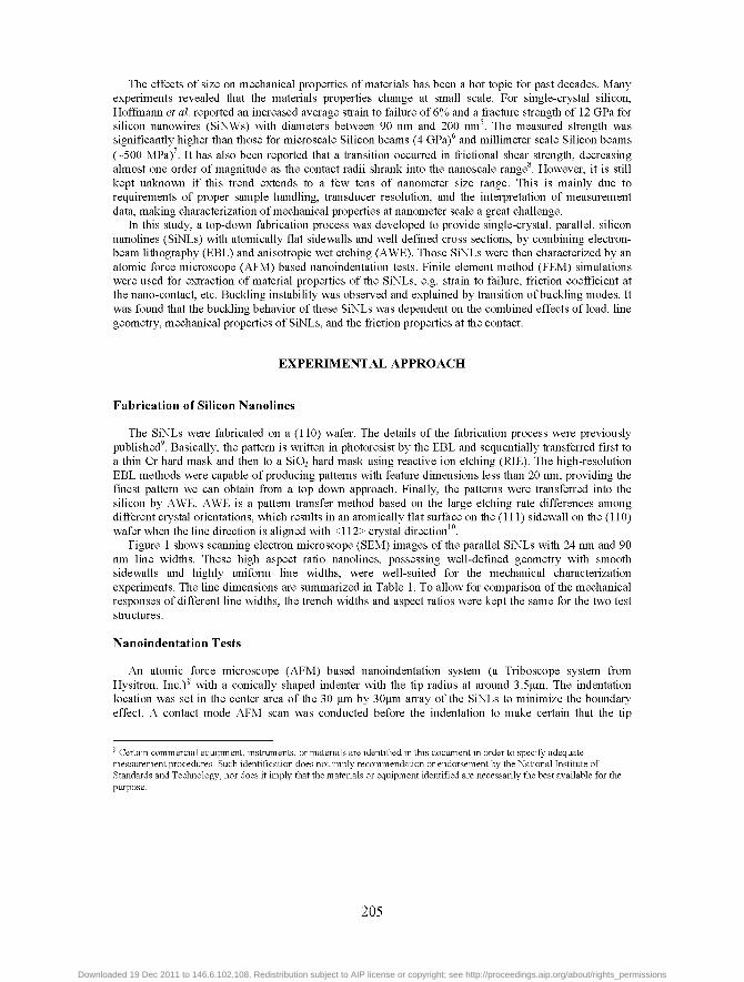
The force-displacement curves obtained from nanoindentation applied to the 24 nm lines are shown in Figure 2. Each complete loop represents an individual test with the upper half for loading and the lower half for unloading. In Figures 2(a) for deformation mode I (DM I) and (b) for DM II, the relatively sharp increase at the beginning of the loading curve (<10 nm) showed the elastic response of the single crystal. The elastic modulus extracted by modeling, later, showed no dramatic change at 24 nm width compared with the bulk silicon. Then, displacement bursts were observed at a critical load 9-30 μN, coincidental with the buckling of the SiNLs. As the load continued to increase, the curves moved up in a stair-like fashion, which was attributed to the indenter making additional contacts with the neighboring SiNLs in the line array. The loading curves reached a maximum displacement of ~220nm, about 58% of the line height, without fracture, exhibiting a large strain-to-fracture for SiNLs at this size scale. After unloading, the curves moved right back to the original start point, making a closed loop, indicating that the displacement was fully recovered with no residual deformation.
Comparing deformation mode I (DM I) in Figure 2(a) with DM II in Figure 2(b), although the indentation load-displacement curves prior to the critical load were almost identical, three major differences were observed from beyond the critical load. The critical load for DM I buckling were 9 to 17 μN, lower than that for DM II buckling (24 to 30 μN). At a load around 70 μN, DM I showed a
206
Downloaded 19 Dec 2011 to 146.6.102.108. Redistribution subject to AIP license or copyright; see http://proceedings.aip.org/about/rights_permissions
displacement of ~220 nm. For the same load, the displacement was only around 80 nm for DM II, indicating a much higher overall stiffness compared with DM I. Since the indentation tests were performed on the same array of SiNLs at different locations, the two different deformation modes were most likely due to the variation in local contact properties arising from surface irregularities of the spherical indenter tip in contact with the SiNLs. It will be discussed later in this paper that the difference in friction coefficient can lead to these distinct buckling modes.
0 60 120 180 240 0 20 40 60 SO 100 Displacement (nm) Displacement (nm)
FIGURE 2. Load vs. displacement curves of nanoindentation tests of the 24 nm SiNLs. Indenter was located on pattern trench center. (a) DM I: critical load ranged from 9 LIN to 17 LIN. (b) DM II: critical load ranged from 24 LIN
to 30 LIN.
Finite Element Method (FEM) Analysis and Friction
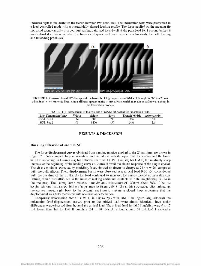
A FEM model was developed to simulate and interpret the nanoindentation experimental results. Detailed descriptions of the FEM model and the experimental procedures have been previously published9, 11. The geometry of the SiNLs and the indenter and their relative positions were set as close to the experimental setup as possible. The indenter and the substrate were modeled as a rigid body. The elastic properties of bulk silicon were used for the properties of the SiNLs, which was reasonable by the close agreement between the loading curves prior to the buckling. This agreement also suggested that the elastic properties of bulk Si reminded unchanged down to linewidths of 24nm. A simple Coulomb friction model was adopted to study the effect of the frictional contact, with friction coefficient varying from 0, i.e. frictionless, to 0.10.
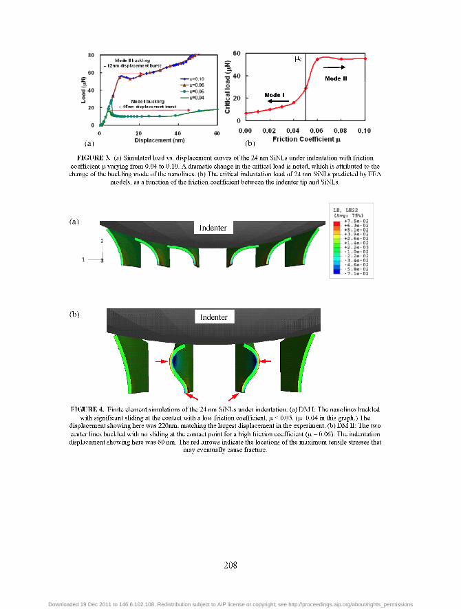
In each simulation, a vertical displacement was applied to the reference node of the indenter, and the reaction force at the reference node was recorded. As shown in Figure 3(a), the simulation results clear show displacement bursts after critical loads, which indicates softening of nanoline structure after buckling. In a displacement controlled simulation, the indentation force dropped after buckling as the displacement kept increasing until more lines were brought into contact, which can be observed in a displacement controlled experiment12. It turned out that friction at contact plays an important role in determining the magnitude of the critical bucking load. Figure 3(b) displays the calculated critical load of indentation on 24 nm SiNLs as a function of friction coefficient LI. It is noted that the critical load increased monotonically with LI.
207
Downloaded 19 Dec 2011 to 146.6.102.108. Redistribution subject to AIP license or copyright; see http://proceedings.aip.org/about/rights_permissions
so
I *
(a)
Mad* II buckling - 12nm displacement bu re t .
M o d e l bUcfcllrcj i,ni ..I •: j •!:•: ••: me nt bure t
20 40 Displacement (nm)
-u-0.10 -u-oos -u-0.05 -u«0.04
60
(b) 0.02 0.04 0.06 0.03
Friction Coefficient ui 0,10
FIGURE 3. (a) Simulated load vs. displacement curves of the 24 nm SiNLs under indentation with friction coefficient μ varying from 0.04 to 0.10. A dramatic change in the critical load is noted, which is attributed to the
change of the buckling mode of the nanolines. (b) The critical indentation load of 24 nm SiNLs predicted by FEA models, as a function of the friction coefficient between the indenter tip and SiNLs.
(Avg: 7SV>
• ! • ! - «
^ ^ | Indenter I ^r^
(b) Indenter |
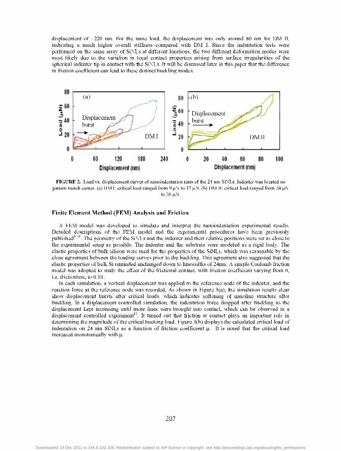
FIGURE 4. Finite element simulations of the 24 nm SiNLs under indentation. (a) DM I: The nanolines buckled with significant sliding at the contact with a low friction coefficient, ii < 0.05. (ii=0.04 in this graph.) The
displacement showing here was 220nm, matching the largest displacement in the experiment. (b) DM II: The two center lines buckled with no sliding at the contact point for a high friction coefficient (ii = 0.06). The indentation displacement showing here was 60 nm. The red arrows indicate the locations of the maximum tensile stresses that
may eventually cause fracture.
208
Downloaded 19 Dec 2011 to 146.6.102.108. Redistribution subject to AIP license or copyright; see http://proceedings.aip.org/about/rights_permissions
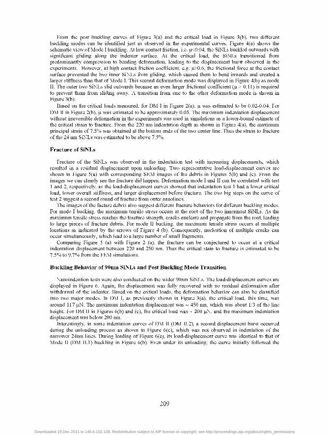
From the post buckling curves of Figure 3(a) and the critical load in Figure 3(b), two different buckling modes can be identified just as observed in the experimental curves. Figure 4(a) shows the schematic view of Mode I buckling. At low contact friction, i.e. μ<0.04, the SiNLs buckled outwards with significant gliding along the indenter surface. At the critical load, the SiNLs transitioned from predominantly compression to bending deformation, leading to the displacement burst observed in the experiments. However, at high contact friction coefficient, e.g. μ>0.6, the frictional force at the contact surface prevented the two inner SiNLs from gliding, which caused them to bend inwards and created a larger stiffness than that of Mode I. This second deformation mode was displayed in Figure 4(b) as mode II. The outer two SiNLs slid outwards because an even larger frictional coefficient (μ > 0.11) is required to prevent them from sliding away. A transition from one to the other deformation mode is shown in Figure 3(b).
Based on the critical loads measured, for DM I in Figure 2(a), μ was estimated to be 0.02-0.04. For DM II in Figure 2(b), μ was estimated to be approximately 0.05. The maximum indentation displacement without irreversible deformation in the experiments was used in simulations as a lower-bound estimate of the critical strain to fracture. From the 220 nm indentation depth as shown in Figure 4(a), the maximum principal strain of 7.5% was obtained at the bottom ends of the two center line. Thus the strain to fracture of the 24 nm SiNLs was estimated to be above 7.5%.
Fracture of SiNLs
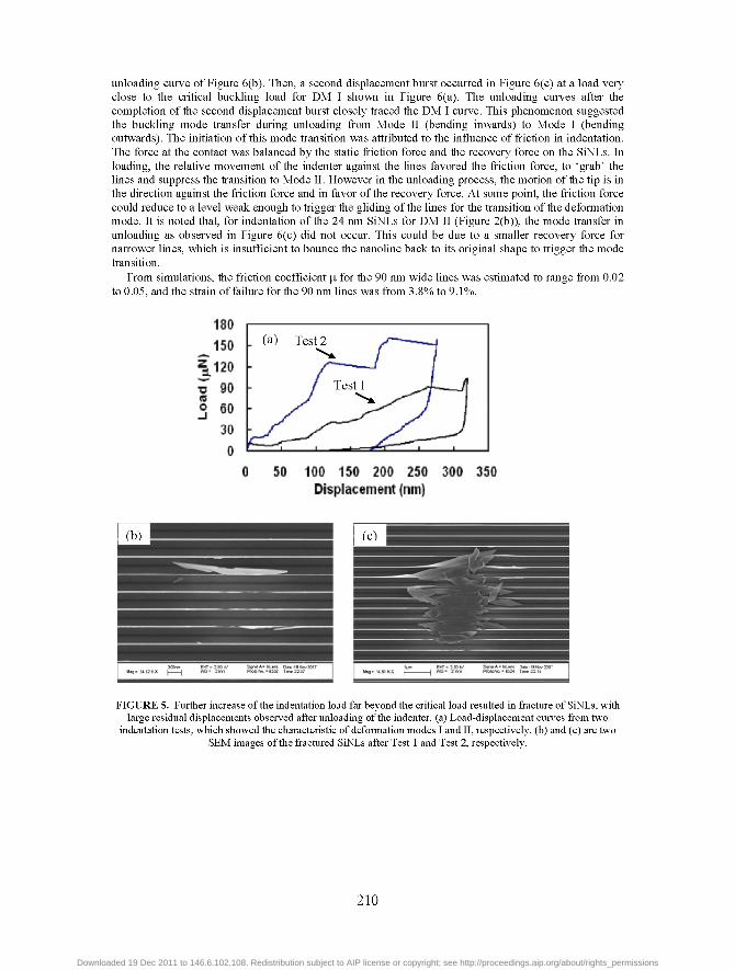
Fracture of the SiNLs was observed in the indentation test with increasing displacements, which resulted in a residual displacement upon unloading. Two representative load-displacement curves are shown in Figure 5(a) with corresponding SEM images of the debris in Figures 5(b) and (c). From the images we can clearly see the fracture did happen. Deformation mode I and II can be correlated with test 1 and 2, respectively, as the load-displacement curves showed that indentation test 1 had a lower critical load, lower overall stiffness, and larger displacement before fracture. The two big steps on the curve of test 2 suggest a second round of fracture from outer nanolines.
The images of the facture debris also suggest different fracture behaviors for different buckling modes. For mode I bucking, the maximum tensile stress occurs at the root of the two innermost SiNLs. As the maximum tensile stress reaches the fracture strength, cracks nucleate and propagate from the root, leading to large pieces of fracture debris. For mode II bucking, the maximum tensile stress occurs at multiple locations as indicated by the arrows of Figure 4 (b). Consequently, nucleation of multiple cracks can occur simultaneously, which lead to a large number of small fragments.
Comparing Figure 5 (a) with Figure 2 (a), the fracture can be conjectured to occur at a critical indentation displacement between 220 and 250 nm. Thus the critical stain to fracture is estimated to be 7.5% to 9.7% from the FEM simulations.
Buckling Behavior of 90nm SiNLs and Post Buckling Mode Transition
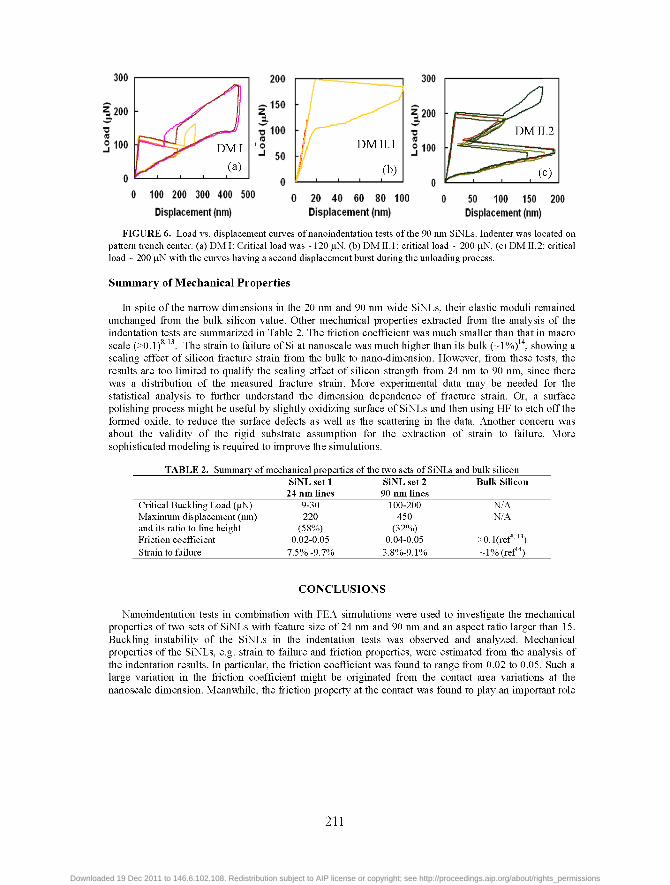
Nanoindention tests were also conducted on the wider 90nm SiNLs. The load-displacement curves are displayed in Figure 6. Again, the displacement was fully recovered with no residual deformation after withdrawal of the indenter. Based on the critical loads, the deformation behavior can also be classified into two major modes. In DM I, as previously shown in Figure 3(a), the critical load, this time, was around 117 μN. The maximum indentation displacement was 450 nm, which was about 1/3 of the line height. For DM II in Figures 6(b) and (c), the critical load was 200 μN, and the maximum indentation displacement was below 200 nm.
Interestingly, in some indentation curves of DM II (DM II.2), a second displacement burst occurred during the unloading process as shown in Figure 6(c), which was not observed in indentation of the narrower 24nm lines. During loading of Figure 6(c), its load-displacement curve was identical to that of Mode II (DM II.1) buckling in Figure 6(b). Even under its unloading, the curve initially followed the
209
Downloaded 19 Dec 2011 to 146.6.102.108. Redistribution subject to AIP license or copyright; see http://proceedings.aip.org/about/rights_permissions
unloading curve of Figure 6(b). Then, a second displacement burst occurred in Figure 6(c) at a load very close to the critical buckling load for DM I shown in Figure 6(a). The unloading curves after the completion of the second displacement burst closely traced the DM I curve. This phenomenon suggested the buckling mode transfer during unloading from Mode II (bending inwards) to Mode I (bending outwards). The initiation of this mode transition was attributed to the influence of friction in indentation. The force at the contact was balanced by the static friction force and the recovery force on the SiNLs. In loading, the relative movement of the indenter against the lines favored the friction force, to ‘grab’ the lines and suppress the transition to Mode II. However in the unloading process, the motion of the tip is in the direction against the friction force and in favor of the recovery force. At some point, the friction force could reduce to a level weak enough to trigger the gliding of the lines for the transition of the deformation mode. It is noted that, for indentation of the 24 nm SiNLs for DM II (Figure 2(b)), the mode transfer in unloading as observed in Figure 6(c) did not occur. This could be due to a smaller recovery force for narrower lines, which is insufficient to bounce the nanoline back to its original shape to trigger the mode transition.
From simulations, the friction coefficient μ for the 90 nm wide lines was estimated to range from 0.02 to 0.05, and the strain of failure for the 90 nm lines was from 3.8% to 9.1%.
0 50 100 150 200 250 300 350 Displacement (urn)
(b) • (c)
FIGURE 5. Further increase of the indentation load far beyond the critical load resulted in fracture of SiNLs, with large residual displacements observed after unloading of the indenter. (a) Load-displacement curves from two
indentation tests, which showed the characteristic of deformation modes I and II, respectively. (b) and (c) are two SEM images of the fractured SiNLs after Test 1 and Test 2, respectively.
210
Downloaded 19 Dec 2011 to 146.6.102.108. Redistribution subject to AIP license or copyright; see http://proceedings.aip.org/about/rights_permissions
Displacement (rim) Displacement (nm) Displacement (nm)
FIGURE 6. Load vs. displacement curves of nanoindentation tests of the 90 nm SiNLs. Indenter was located on pattern trench center. (a) DM I: Critical load was 120 μN. (b) DM II.1: critical load 200 μN. (c) DM II.2: critical load 200 μN with the curves having a second displacement burst during the unloading process.
Summary of Mechanical Properties
In spite of the narrow dimensions in the 20 nm and 90 nm wide SiNLs, their elastic moduli remained unchanged from the bulk silicon value. Other mechanical properties extracted from the analysis of the indentation tests are summarized in Table 2. The friction coefficient was much smaller than that in macro scale (>0.1)8, 13. The strain to failure of Si at nanoscale was much higher than its bulk (~1%)14, showing a scaling effect of silicon fracture strain from the bulk to nano-dimension. However, from these tests, the results are too limited to qualify the scaling effect of silicon strength from 24 nm to 90 nm, since there was a distribution of the measured fracture strain. More experimental data may be needed for the statistical analysis to further understand the dimension dependence of fracture strain. Or, a surface polishing process might be useful by slightly oxidizing surface of SiNLs and then using HF to etch off the formed oxide, to reduce the surface defects as well as the scattering in the data. Another concern was about the validity of the rigid substrate assumption for the extraction of strain to failure. More sophisticated modeling is required to improve the simulations.
TABLE 2. Summary of mechanical properties of the two sets of SiNLs and bulk silicon
Critical Buckling Load (μN) Maximum displacement (nm) and its ratio to line height Friction coefficient Strain to failure
SiNL set 1 24 nm lines
9-30 220
(58%) 0.02-0.05
7.5% -9.7%
SiNL set 2 90 nm lines
100-200 450
(32%) 0.04-0.05
3.8%-9.1%
Bulk Silicon
N/A N/A
>0.1(ref8, 13) ~ 1 % (ref14)
CONCLUSIONS
Nanoindentation tests in combination with FEA simulations were used to investigate the mechanical properties of two sets of SiNLs with feature size of 24 nm and 90 nm and an aspect ratio larger than 15. Buckling instability of the SiNLs in the indentation tests was observed and analyzed. Mechanical properties of the SiNLs, e.g. strain to failure and friction properties, were estimated from the analysis of the indentation results. In particular, the friction coefficient was found to range from 0.02 to 0.05. Such a large variation in the friction coefficient might be originated from the contact area variations at the nanoscale dimension. Meanwhile, the friction property at the contact was found to play an important role
211
Downloaded 19 Dec 2011 to 146.6.102.108. Redistribution subject to AIP license or copyright; see http://proceedings.aip.org/about/rights_permissions
in controlling the buckling behavior of SiNLs. The strain to fracture of the SiNLs was estimated ranging from 3.8% to 9.7%, which is consistent with the previous results9. This study demonstrated a valuable approach for characterization of mechanical properties at the nanoscale. Further study is ongoing to understand the dimension dependence on fracture strain.
ACKNOWLEDGMENTS
The authors thank Dr. Li Shi for helpful discussion on the fabrication process development. This work was performed in part at the Microelectronics Research Center of the University of Texas at Austin, a member of the National Nanofabrication Infrastructure Network supported by the National Science Foundation under Grant No. 0335765. MKK and RH are grateful for the financial support by the National Science Foundation through Grant No. CMMI-0654105. We are also grateful to the NIST Office of Microelectronics Programs for supporting this work.
REFERENCES
1. M. Li, H. X. Tang and M. L. Roukes, Nat. Nanotechnol. 2 (2), 114-120 (2007). 2. S. Wei-Chuan, K. Sang-Gook and G. Barbastathis, Microelectromechanical Systems, Journal of 15 (4),
763-769 (2006). 3. J. Xiang, W. Lu, Y. J. Hu, Y. Wu, H. Yan and C. M. Lieber, Nature 441 (7092), 489-493 (2006). 4. D. Rugar, R. Budakian, H. J. Mamin and B. W. Chui, Nature 430 (6997), 329-332 (2004). 5. S. Hoffmann, I. Utke, B. Moser, J. Michler, S. H. Christiansen, V. Schmidt, S. Senz, P. Werner, U. Gosele
and C. Ballif, Nano Letters 6 (4), 622-625 (2006). 6. S. Johansson, J. A. Schweitz, L. Tenerz and J. Tiren, Journal of applied physics 63 (10), 4799-4803 (1988). 7. T. Namazu, Y. Isono and T. Tanaka, Microelectromechanical Systems, Journal of 9 (4), 450-459 (2000). 8. D. W. Xu, K. Ravi-Chandar and K. A. Liechti, J. Colloid Interface Sci. 318 (2), 507-519 (2008). 9. B. Li, M. K. Kang, K. Lu, R. Huang, P. S. Ho, R. A. Allen and M. W. Cresswell, Nano Letters 8 (1), 92-98
(2008). 10. M. W. Cresswell, W. F. Guthrie, R. G. Dixson, R. A. Allen, C. E. Murabito and J. V. M. De Pinillos,
Journal of Research of the National Institute of Standards and Technology 111 (3), 187-203 (2006). 11. M. K. Kang, B. Li, P. S. Ho and R. Huang, J. Nanomater., 11 (2008). 12. Z. Luo, the University of Texas at Austin, 2009 13. B. Bhushan and X. D. Li, J. Mater. Res. 12 (1), 54-63 (1997). 14. R. F. Cook, Journal of Materials Science 41 (3), 841-872 (2006).
212
Downloaded 19 Dec 2011 to 146.6.102.108. Redistribution subject to AIP license or copyright; see http://proceedings.aip.org/about/rights_permissions