Embed Size (px)
Citation preview
Nanoelectronics is changing the way the world communicates, and is transforming our daily lives. Continuing Moore’s law and miniaturization of low-power semiconductor chips with ever-increasing functionality have been relentlessly driving R&D of new devices, materials, and process capabilities to meet performance, power, and cost requirements. This book covers up-to-date advances in research and industry practices in nanometrology, critical for continuing technology scaling and product innovation. It holistically approaches the subject matter and addresses emerging and important topics in semiconductor R&D and manufacturing. It is a complete guide for metrology and diagnostic techniques essential for process technology, electronics packaging, and product development and debugging—a unique approach compared to other books. The authors are from academia, government labs, and industry and have vast experience and expertise in the topics presented. The book is intended for all those involved in IC manufacturing and nanoelectronics and for those studying nanoelectronics process and assembly technologies or working in device testing, characterization, and diagnostic techniques.
Zhiyong Ma received his MS degree in materials engineering from Purdue University, Indiana, and a PhD in materials science and engineering from the University of Illinois, Urbana-Champaign. He worked in thin-film metallization and processing at Digital Equipment Corporation and joined Intel’s Corporate Quality Network in 1995. Currently, he is vice president of the Technology and Manufacturing Group and director of Technology Development and Manufacturing Labs at Intel, responsible for
the CQN lab network in support of silicon and assembly technology development and manufacturing, product fault diagnostics, and silicon and platform benchmarking, including strategic business planning, analytical technique development, and metrology roadmaps. Dr. Ma holds 8 patents in underbump metallization, strained silicon transistors, secured fuse technology, and silicon diagnostic techniques, has published more than 25 refereed papers, and has coauthored a book chapter on silicide technology. His research interests include thin-film kinetics, analytical techniques and metrology, and product fault diagnostics.
David G. Seiler received his PhD and MS in physics from Purdue University and a BS in physics from Case Western Reserve University, Ohio. He is a fellow of the American Physical Society and a fellow of the Institute of Electrical and Electronic Engineers. In 2000, he received a Distinguished Alumni Award from Purdue University’s School of Science for his contributions to and achievements in semiconductors. He served as solid state physics program director in the Materials Research Division,
National Science Foundation; spent a year’s sabbatical at the MIT Francis Bitter National Magnet Laboratory; and was a regents’ professor of physics at the University of North Texas. He joined the National Institute of Standards and Technology (NIST) in 1988 and served as program analyst in the program office for the director of NIST and as materials technology group leader in the Engineering Physics Division. Currently, he is chief of the division, which provides technical leadership inmeasurement science research, development, and standards essential to improving US economiccompetitiveness for advanced manufacturing. Dr. Seiler has been the chairperson and proceedingseditor of 15 international conferences or workshops. He is the coeditor and coauthor of a chapterin Semiconductors and Semimetals (1992, Vol. 36) and a coauthor of a chapter in Handbook of Optics(1995, revised 2009). His current research focus is on understanding and advancing the metrologyand characterization measurements needed for the future of nanoelectronics. The results of hisresearch have been disseminated in over 200 publications and 100 talks throughout the world.
Ma
Seiler
Zhiyong MaDavid G. Seiler
edited by
Metrology and DiagnosticTechniques for Nanoelectronics
Metrology and Diagnostic Techniques for Nanoelectronics
ISBN 978-981-4745-08-6V513

Metrology and Diagnostic Techniques for Nanoelectronics
Metrology and Diagnostic Techniques for Nanoelectronics


for the WorldWind PowerThe Rise of Modern Wind Energy
Preben MaegaardAnna KrenzWolfgang Palz
editors
Pan Stanford Series on Renewable Energy — Volume 2
Zhiyong MaDavid G. Seiler
edited by
Metrology and Diagnostic Techniques for Nanoelectronics
Published by
Pan Stanford Publishing Pte. Ltd.Penthouse Level, Suntec Tower 3 8 Temasek Boulevard Singapore 038988
Email: [email protected] Web: www.panstanford.com
British Library Cataloguing-in-Publication DataA catalogue record for this book is available from the British Library.
Metrology and Diagnostic Techniques for NanoelectronicsCopyright © 2017 by Pan Stanford Publishing Pte. Ltd.All rights reserved. This book, or parts thereof, may not be reproduced in any form or by any means, electronic or mechanical, including photocopying, recording or any information storage and retrieval system now known or to be invented, without written permission from the publisher.
For photocopying of material in this volume, please pay a copying fee through the Copyright Clearance Center, Inc., 222 Rosewood Drive, Danvers, MA 01923, USA. In this case permission to photocopy is not required from the publisher.
Cover image courtesy: Lapp Group, Germany
ISBN 978-981-4745-08-6 (Hardcover)ISBN 978-981-4745-09-3 (eBook)
Printed in the USA
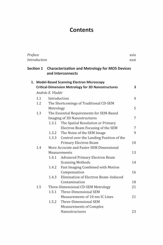
Contents
Preface xxixIntroduction xxxi
Section 1 Characterization and Metrology for MOS Devices and Interconnects
1. Model-Based Scanning Electron Microscopy Critical-Dimension Metrology for 3D Nanostructures 3
Andras E. Vladar
1.1 Introduction 4 1.2 The Shortcomings of Traditional CD-SEM
Metrology 5 1.3 The Essential Requirements for SEM-Based
Imaging of 3D Nanostructures 7 1.3.1 The Spatial Resolution or Primary
Electron Beam Focusing of the SEM 7 1.3.2 The Noise of the SEM Image 9 1.3.3 Control over the Landing Position of the
Primary Electron Beam 10 1.4 More Accurate and Faster SEM Dimensional
Measurements 13 1.4.1 Advanced Primary Electron Beam
Scanning Methods 14 1.4.2 Fast Imaging Combined with Motion
Compensation 16 1.4.3 Elimination of Electron Beam–Induced
Contamination 18 1.5 Three-Dimensional CD-SEM Metrology 21 1.5.1 Three-Dimensional SEM
Measurements of 10 nm IC Lines 21 1.5.2 Three-Dimensional SEM
Measurements of Complex Nanostructures 23
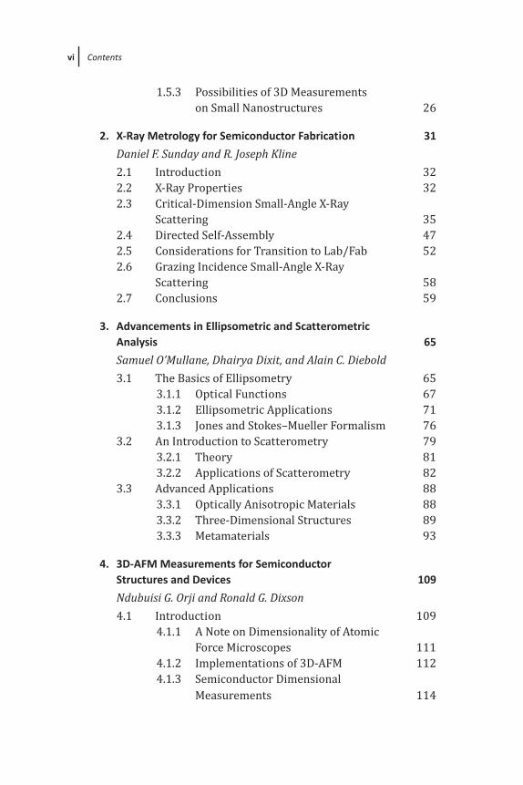
vi Contents
1.5.3 Possibilities of 3D Measurements on Small Nanostructures 26
2. X-Ray Metrology for Semiconductor Fabrication 31
Daniel F. Sunday and R. Joseph Kline
2.1 Introduction 322.2 X-Ray Properties 322.3 Critical-Dimension Small-Angle X-Ray
Scattering 352.4 Directed Self-Assembly 472.5 Considerations for Transition to Lab/Fab 522.6 Grazing Incidence Small-Angle X-Ray
Scattering 582.7 Conclusions 59
3. Advancements in Ellipsometric and ScatterometricAnalysis 65
Samuel O’Mullane, Dhairya Dixit, and Alain C. Diebold
3.1 The Basics of Ellipsometry 653.1.1 Optical Functions 673.1.2 Ellipsometric Applications 713.1.3 Jones and Stokes–Mueller Formalism 76
3.2 An Introduction to Scatterometry 793.2.1 Theory 813.2.2 Applications of Scatterometry 82
3.3 Advanced Applications 883.3.1 Optically Anisotropic Materials 883.3.2 Three-Dimensional Structures 893.3.3 Metamaterials 93
4. 3D-AFM Measurements for SemiconductorStructures and Devices 109
Ndubuisi G. Orji and Ronald G. Dixson
4.1 Introduction 1094.1.1 A Note on Dimensionality of Atomic
Force Microscopes 1114.1.2 Implementations of 3D-AFM 1124.1.3 Semiconductor Dimensional
Measurements 114
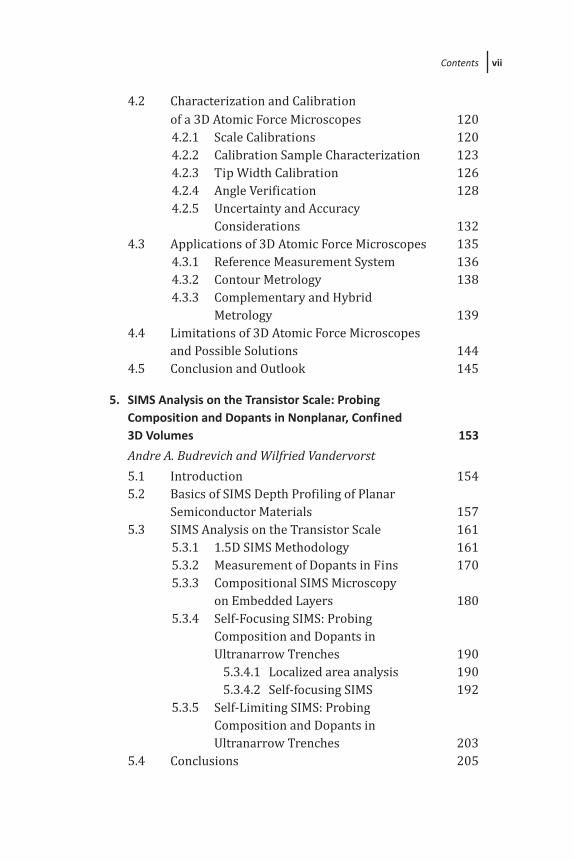
viiContents
4.2 Characterization and Calibration of a 3D Atomic Force Microscopes 1204.2.1 Scale Calibrations 1204.2.2 Calibration Sample Characterization 1234.2.3 Tip Width Calibration 1264.2.4 Angle Verification 1284.2.5 Uncertainty and Accuracy
Considerations 1324.3 Applications of 3D Atomic Force Microscopes 135
4.3.1 Reference Measurement System 1364.3.2 Contour Metrology 1384.3.3 Complementary and Hybrid
Metrology 1394.4 Limitations of 3D Atomic Force Microscopes
and Possible Solutions 1444.5 Conclusion and Outlook 145
5. SIMS Analysis on the Transistor Scale: ProbingComposition and Dopants in Nonplanar, Confined3D Volumes 153
Andre A. Budrevich and Wilfried Vandervorst
5.1 Introduction 1545.2 Basics of SIMS Depth Profiling of Planar
Semiconductor Materials 1575.3 SIMS Analysis on the Transistor Scale 161
5.3.1 1.5D SIMS Methodology 1615.3.2 Measurement of Dopants in Fins 1705.3.3 Compositional SIMS Microscopy
on Embedded Layers 1805.3.4 Self-Focusing SIMS: Probing
Composition and Dopants in Ultranarrow Trenches 190
5.3.4.1 Localized area analysis 1905.3.4.2 Self-focusing SIMS 192
5.3.5 Self-Limiting SIMS: Probing Composition and Dopants in Ultranarrow Trenches 203
5.4 Conclusions 205
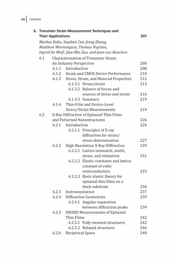
viii Contents
6. Transistor Strain Measurement Techniques and Their Applications 207
Markus Kuhn, Stephen Cea, Jiong Zhang, Matthew Wormington, Thomas Nuytten, Ingrid De Wolf , Jian-Min Zuo, and Jean-Luc Rouviere
6.1 Characterization of Transistor Strain: An Industry Perspective 208
6.1.1 Introduction 208 6.1.2 Strain and CMOS Device Performance 210 6.1.3 Stress, Strain, and Material Properties 212 6.1.3.1 Stress/strain 213 6.1.3.2 Balance of forces and
sources of stress and strain 216 6.1.3.3 Summary 219 6.1.4 Thin-Film and Device-Level
Stress/Strain Measurements 219 6.2 X-Ray Diffraction of Epitaxial Thin Films
and Patterned Nanostructures 226 6.2.1 Introduction 226 6.2.1.1 Principles of X-ray
diffraction for strain/ stress determination 227
6.2.2 High-Resolution X-Ray Diffraction 229 6.2.2.1 Lattice mismatch, misfit,
strain, and relaxation 231 6.2.2.2 Elastic constants and lattice
constant of cubic semiconductors 233
6.2.2.3 Basic elastic theory for epitaxial thin films on a thick substrate 236
6.2.3 Instrumentation 237 6.2.4 Diffraction Geometries 239 6.2.4.1 Angular separation
between diffraction peaks 239 6.2.5 HRXRD Measurements of Epitaxial
Thin Films 242 6.2.5.1 Fully strained structures 242 6.2.5.2 Relaxed structures 246 6.2.6 Reciprocal Space 248
ixContents
6.2.6.1 Scans and maps in reciprocal space 251
6.2.7 Reciprocal Space Maps of Thin Films 252 6.2.8 Reciprocal Space Maps of Patterned
Nanostructures 258 6.2.8.1 Periodicity and shape/
size analysis 258 6.2.8.2 Strain/stress and
composition analysis 262 6.2.9 Synchrotron Studies 269 6.2.9.1 Microbeam X-ray diffraction
and topography 270 6.2.9.2 Nanobeam reciprocal space
mapping 272 6.2.9.3 Bragg projection X-ray
ptychography 273 6.2.10 Conclusion and Outlook 274 6.3 Strain Measurement Using Advanced
Raman Spectroscopy 275 6.3.1 Raman Spectroscopy: Theory and
Early History 275 6.3.2 Micro-Raman Spectroscopy 278 6.3.3 Novel Approaches and State of the Art 284 6.3.3.1 Resonant Raman
enhancement 284 6.3.3.2 Surface-enhanced Raman
spectroscopy 285 6.3.3.3 Tip-enhanced Raman
spectroscopy 287 6.3.3.4 Edge-enhanced Raman
spectroscopy 290 6.3.4 Summary 293 6.4 Transistor Strain Measurement Using
Electron Beam Techniques 294 6.4.1 Introduction to Strain and Stress 296 6.4.1.1 Strain and stress 296 6.4.1.2 Definition of strain 297 6.4.1.3 Theoretical modeling of
strain and stress 299 6.4.1.4 Measurement of strain
and stress 300
x Contents
6.4.1.5 Strain and stress in nanoelectronic devices 300
6.4.2 An Overview of Electron Beam–Based Strain Measurement Techniques 302
6.4.2.1 Transmission electron microscopy 302
6.4.2.2 Electron beam–based strain measurement techniques and capabilities 305
6.4.2.3 TEM sample preparation 310 6.4.2.4 The limitations of electron
beam techniques 312 6.4.3 Principles of Electron
Diffraction–Based Strain Measurement Techniques and Applications 314
6.4.3.1 Nanobeam electron diffraction 314
6.4.3.2 Convergent beam electron diffraction 328
6.4.4 Principles of Electron Imaging–Based Strain Measurement Techniques and Applications 335
6.4.4.1 HREM 335 6.4.4.2 Strain mapping using GPA 339 6.4.4.3 STEM and its application
for strain measurements 340 6.4.4.4 Dark-field electron
holography 348 6.4.5 Conclusions 352
7. Scanning Spreading Resistance Microscopy (SSRM): High-Resolution 2D and 3D Carrier Mapping of Semiconductor Nanostructures 377
Andreas Schulze, Pierre Eyben, Thomas Hantschel, and Wilfried Vandervorst
7.1 Introduction 378 7.2 Fundamentals of SSRM 379 7.2.1 Basic Principle 379 7.2.2 Physics of the Spreading Resistance 380
xiContents
7.2.2.1 Maxwell’s spreading resistance equation 380
7.2.2.2 Sharvin’s law 3827.2.3 SSRM on Silicon 384
7.2.3.1 Electrical contact properties 3867.2.3.2 Surface states 387
388388
7.2.4 SSRM on Germanium 7.2.4.1 Electrical contact properties7.2.4.2 Surface states 3907.2.4.3 Trap-assisted tunneling 391
7.2.5 Quantification of SSRM Raw Data 3927.2.5.1 Homostructures 3927.2.5.2 Heterostructures 396
7.2.6 SSRM Probes 3977.2.7 Environmental Aspects 4057.2.8 Sample Preparation 406
7.2.8.1 Device cross-sectioning 4067.2.8.2 Electrical back-contact 407
7.2.9 Three-Dimensional Carrier Mapping 4087.3 SSRM on Advanced 3D Semiconductor
Devices 4097.3.1 SSRM on Nanowire-Based All-Silicon
TFET 4097.3.1.1 Device configuration 4097.3.1.2 SSRM carrier maps 4117.3.1.3 Diameter-dependent boron
diffusion 4127.3.2 SSRM on Nanowire-Based
Heterojunction TFET 416416417
7.3.3 SSRM on InP Fin Structure 4247.4 Fast Fourier Transform-SSRM 426
7.4.1 FFT-SSRM: Principle of Operation 427
7.4.2 Force Regime for FFT-SSRM 4307.4.3 Implementation of FFT-SSRM 431
7.4.3.1 One-dimensional FFT-SSRM 4317.4.3.2 Two-dimensional FFT-SSRM 434
7.3.2.1 Device configuration7.3.2.2 SSRM carrier maps
xii Contents
7.4.4 FFT-SSRM in the Presence of Series Resistances 435
7.5 Summary 438
8. Microstructure Characterization of Nanoscale Materials and Interconnects 447
J. K. Weiss, Jai Ganesh Kameswaran, Amith Darbal, Jiong Zhang, Di Xu, and Edgar F. Rauch
8.1 Structure/Property Relationships of Interconnects 448
8.1.1 Reliability 449 8.1.1.1 Electromigration 449 8.1.1.2 Stress-induced voiding 451 8.1.2 Electrical Resistivity 453 8.2 Microstructure Characterization Techniques
for Interconnects 454 8.2.1 Traditional Techniques to
Characterize Microstructure 454 8.2.1.1 Scanning electron
microscopy and focused ion beam 454
8.2.1.2 Electron backscattering diffraction 455
8.2.1.3 TEM and STEM imaging 456 8.2.2 Emerging Techniques for
Nanostructure Characterization 457 8.2.2.1 Three-dimensional EBSD
development 457 8.2.2.2 Automated crystal
orientation mapping with NBD 458
8.2.2.3 Transmission Kikuchi diffraction in SEM 458
8.2.3 Concluding Remarks on Techniques 459 8.3 Automated Crystal Orientation Mapping
Using NBD 459 8.3.1 Indexing Spot Diffraction Patterns
through Template Matching 460 8.3.2 Spatial and Angular Resolution
and Limitations 461
xiiiContents
8.4 Precession Electron Diffraction 465 8.5 Experimental Considerations 470 8.5.1 Specimen Preparation 471 8.5.2 Prespecimen Electron Optics 472 8.5.3 Postspecimen Electron Optics 474 8.5.4 Diffraction Pattern Recording 475 8.6 Applications of ACOM with PED 476
9. Characterization of the Chemistry and Mechanical Properties of Interconnect Materials and Interfaces: Impact on Interconnect Reliability 493
Ying Zhou and Han Li 9.1 Introduction 494 9.2 Surface and Interface Chemical Structure
Characterization 495 9.2.1 Surface Chemical Structure of Low-k
Dielectrics and Process Impacts 497 9.2.2 Cu Surface and Film Chemistry
Analyses 502 9.2.3 Characterization of Interfaces 504 9.3 Progress in Characterizing the Adhesion,
Fracture, and Mechanical Properties of Thin Films and Interconnect Structures 508
9.3.1 Overview of Mechanical Characterization Techniques and Recent Advancements 508
9.3.2 Buffer Layer Structures for Characterizing Mechanical Properties of Nanoporous Low-k Dielectrics 511
9.3.3 Superlayer Structures for Adhesion and Fracture Measurement of Ultrathin-Film Stacks 517
9.3.4 Controlled Fracture of Integrated Structures 521
9.3.5 Future Challenges and Opportunities 525 9.4 Integrated Studies of Surface and Interface
Chemistry, Adhesion, and Electromigration Reliability 526
9.4.1 Cu Barrier/ILD Interface 527
xiv Contents
9.4.2 Etch Stop/Cu Interface 5299.5 Concluding Remarks and Future Prospects 534
10. Characterization of Plasma Damage for Low-kDielectric Films 541
Hualiang Shi, Huai Huang, Ryan S. Smith,and Paul S. Ho10.1 Introduction 54210.2 Molecular Bonding Characteristics of
Low-k Dielectrics 54410.3 CO2 Plasma-Induced Damage to Porous
Low-k Dielectrics 54810.3.1 Bonding Configuration Changes 54910.3.2 Depth of Carbon Depletion Layer 55010.3.3 Film Shrinkage and Densification 55110.3.4 Increase of the Effective Dielectric Constant 553
10.4 Role of Plasma Species on Plasma Damage of Porous Low-k Dielectrics 55310.4.1 Effect of Radical Density 55610.4.2 Effect of Ion Energy 55910.4.3 Effect of Photon Energy and Intensity 56110.4.4 Effect of Low-k Pore Size and Porosity 565
10.5 Kinetic Models for Plasma Damage Formation in Low-k Dielectrics 56610.5.1 Plasma-Altered Layer Model 56710.5.2 Sputtering Yield Model 570
10.6 Dielectric Recovery of Plasma Damage 57210.6.1 Dielectric Recovery by Silylation 57310.6.2 Dielectric Recovery by UV Irradiation 578
10.7 Conclusions 581
11. Defect Characterization and Metrology 589
Tuyen K. Tran11.1 Introduction to Defect Characterization 58911.2 Unpatterned Defect Inspection: Past,
Present, and Future 59211.3 Patterned Defect Inspection: Past, Present,
and Future 60711.3.1 Dark-Field Inspection Technology 607
xvContents
11.3.2 Bright-Field Defect Inspection 614 11.3.3 Electron Beam Defect Inspection 621 11.4 Conclusion and Outlook 626
12. 3D Electron Tomography for Nanostructures 637
Huolin L. Xin, Sai Bharadwaj Vishnubhotla, and Ruoqian Lin
12.1 History 638 12.2 Concepts of Tomography 639 12.2.1 Radon Transformation 639 12.2.2 Central Slice Theorem and Fourier
Space Reconstruction 640 12.2.3 Back Projection: Real Space
Reconstruction 641 12.2.3.1 Important parameters
and aspects of electron tomography 642
12.3 Types of Tomography 644 12.3.1 HAADF (Z-Contrast) Tomography 644 12.3.2 Incoherent Bright-Field STEM
Tomography 646 12.3.3 EFTEM Tomography 649 12.3.4 STEM-EELS Tomography 651 12.3.5 STEM-EDS Tomography 652 12.4 Applications 654 12.4.1 Electron Tomography for
Characterizing Copper Interconnects 655 12.4.2 Chemical 3D Tomography for High-k
Dielectrics 657 12.4.3 Imaging of Pore Structures of Low-k
Dielectrics by 3D Tomography 658 12.5 Conclusions 659
13. Electron Energy Loss Spectroscopy of Semiconductor Nanostructures and Oxides 663
Wu Zhou, Maria Varela, Juan-Carlos Idrobo, Sokrates T. Pantelides, and Stephen J. Pennycook
13.1 Introduction 664 13.2 General Principles of EELS 665 13.3 Applications 669
xvi Contents
13.3.1 STEM-EELS with Atomic Column Sensitivity at the CoSi2/Si and SiO2/ Si Interfaces 669
13.3.2 STEM-EELS Analysis at the Single-Atom Level 670
13.3.3 STEM-EELS Mapping on Complex-Oxide Thin Films 684
13.3.4 Low-Loss EELS for Valence Excitations 690
13.4 Perspectives 696
14. Atom Probe Tomography of Semiconductor Nanostructures 711
Thomas F. Kelly and Karen Henry
14.1 Introduction 711 14.2 Overview of Atom Probe Tomography 712 14.2.1 Essentials of How It Works 712 14.2.2 Composition Determination 714 14.2.3 Constructing the 3D Image 716 14.2.4 Spatial Scaling 717 14.2.5 FIB-Based Specimen Preparation 718 14.2.6 Relevant Strengths and Limitations
of APT for Metrology 718 14.2.7 Compositional Fidelity 721 14.2.8 Spatial Distortions 723 14.3 Application of APT to Semiconductor
Metrology 723 14.3.1 WorkflowforTypicalApplications 725 14.3.2 Critical Applications at Present 727 14.3.2.1 Multilayer structures 727 14.3.2.2 High-k applications 728 14.3.2.3 Silicide applications 730 14.3.2.4 MOSFET structures 732 14.3.2.5 FinFET structures 734 14.3.2.6 Fully processed devices 735 14.3.3 Critical Applications in the Near
Future 737 14.3.3.1 Alternative channel
materials: group IV 737
xviiContents
14.3.3.2 Alternative channel materials: group III–V compounds 738
14.3.3.3 New architectures: nanowires 740
14.4 Roadmap for Metrology Improvement 74514.5 Conclusion 747
Section 2 Characterization Techniques for Novel Materials and Devices beyond CMOS
15. Characterization and Metrology for GrapheneMaterials, Structures, and Devices 759
Luigi Colombo, Alain Diebold, Cinzia Casiraghi,Moon Kim, Robert M. Wallace, andArchana Venugopal15.1 Introduction 760
15.1.1 Graphene Preparation Processes 76415.1.2 Graphene Devices and Structures 765
15.2 Physical Characterization 76715.2.1 Optical Microscopy 76915.2.2 Scanning Electron Microscopy 77115.2.3 Scanning Tunneling Microscopy 77115.2.4 Raman Spectroscopy 77315.2.5 X-Ray Photoelectron Spectroscopy 78515.2.6 Low-Energy Electron and Ion
Techniques 79315.2.6.1 Low-energy electron
diffraction 79315.2.6.2 Low-energy electron
microscopy 79315.2.6.3 Low-energy ion
spectroscopy 79415.2.7 X-Ray Diffraction 79415.2.8 Transmission Electron Microscopy 795
15.2.8.1 TEM sample preparation 79515.2.8.2 TEM techniques 79815.2.8.3 Grain morphology and
growth behavior 79815.2.8.4 Layers and stacking 803
xviii Contents
15.2.8.5 High-resolution TEM imaging 80515.2.8.6 Atomic-resolution
spectroscopy 80715.2.8.7 In situ study 80815.2.8.8 Graphene as a template
substrate for 2D TMD growth 81015.3 Optical Characterization 812
812
812
Optical Properties of Graphene 81315.3.4 Dielectric Function in Deep VUV 814
15.4 Electrical Characterization 81515.4.1 Kelvin Probe Method 81515.4.2 R–Vgs Characteristics 81515.4.3 Contact Resistance 817
15.4.3.1 Transfer length method 81815.4.4 Mobility 81915.4.5 Spin-Based Transport 822
15.5 Summary 822
16. Characterization of Magnetic Nanostructuresfor Spin-Torque Memory Applications withMacro- and Microscale Ferromagnetic Resonance 849
T. J. Silva, H. T. Nembach, J. M. Shaw, Brian Doyle,Kaan Oguz, Kevin O’brien, and Mark Doczy
16.1 Background: Spin-Torque RAM andFerromagnetic Resonance 85016.1.1 Figures of Merit for Write
Efficiency: Anisotropy and Damping 85016.1.2 Magnetization Dynamics and
Ferromagnetic Resonance 85116.2 Measurement Methods: VNA-FMR 854
16.2.1 Basics of the Measurement Procedure 854
16.2.2 VNA-FMR Measurement Physics 85516.2.3 Excitation Field Details 85816.2.4 CPW Design Considerations 861
15.3.1 THz Optical Properties 15.3.2 Infrared Optical Properties of Graphene15.3.3 Near-Infrared, Visible, and UV
xixContents
16.2.5 Sample–CPW Interactions: Eddy Currents and Capacitive Shunting 863
16.2.6 Extraction of the Damping Parameter α: The Case of CoFeB/MgO Sandwich Structures 865
16.2.7 Limits for the Use of Damping Measurements with Blanket Films 867
16.3 Measurement Methods: H-MOMM 869 16.3.1 Basics of Heterodyne Magneto-Optic
Microwave Magnetometry 869 16.3.2 Signal-to-Noise Ratio for H-MOMM 871 16.3.3 Details of Signal Detection 877 16.3.4 Spectra and Damping for Individual,
In-Plane-Oriented Permalloy Nanomagnets, and Evidence for Curvature-Dependent, Nonlocal Damping 879
16.3.5 Considerations for Use of H-MOMM in a Perpendicular Geometry 882
17. Band Alignment Measurement by Internal Photoemission Spectroscopy 891
Nhan V. Nguyen 17.1 Introduction 892 17.2 Basic Principle of Internal Photoemission 895 17.2.1 Internal Photoemission Process 895 17.2.1.1 Optical excitation 896 17.2.1.2 Transport to the interface 899 17.2.1.3 Escape over the barrier 900 17.2.2 Barrier Height Lowering 901 17.3 IPE Measurements and Hole Emission 903 17.3.1 Measurements 903 17.3.2 Hole Emission Detection 904 17.4 Application as Threshold Spectroscopy 907 17.4.1 Metal/SiO2/Si 908 17.4.2 Semiconductor Heterojunctions 909 17.4.2.1 InAs/AlGaSb heterojunction 910 17.4.2.2 InAs/GaSb 914 17.4.3 Direct Measurement of the Intrinsic
Work Function and Band Alignment of Graphene 919
17.5 Summary 926
xx Contents
Section 3 Electrical Characterization and Reliability Testing Techniques
18. Electrical Characterization of Nanoscale Transistors: Emphasis on Traps Associated with MOS Gate Stacks 933
Xiao Sun and T. P. Ma 18.1 Introduction 934 18.2 Traps in MOS Devices: Origins and Impacts 934 18.2.1 Interface Traps 935 18.2.2 Border and Oxide Traps 938 18.3 Electrical Characterization Methods for
Traps in MOS Devices 941 18.3.1 Based on DC Id–Vg Measurements 941 18.3.2 Gate Admittance Methods 943 18.3.3 Gate Admittance as Affected by
Border Traps 946 18.3.4 Charge Pumping Method 947 18.3.5 Limitations of Gate Admittance
and Charge Pumping Methods 950 18.3.6 Noise Measurements 951 18.3.7 AC Transconductance Method 954 18.3.7.1 AC transconductance
method for characterizing interface traps 954
18.3.7.2 AC transconductance method for characterizing slow traps 955
18.3.8 Pulsed I–V and Time-Dependent Defect Spectroscopy 962
18.3.9 Inelastic Electron Tunneling Spectroscopy 964
19. Charge Pumping for Reliability Characterization and Testing of Nanoelectronic Devices 977
Jason T. Ryan, Jason P. Campbell, Kin P. Cheung, and John S. Suehle
19.1 Introduction 978 19.2 The Basic Charge-Pumping Method 978 19.3 Measurement Considerations: Transition
Times 980
xxiContents
19.4 Measurement Considerations: Incomplete Trap Filling 982
19.5 Measurement Considerations: Gate Leakage Current and Mitigation Methods 984
19.6 Interface Defect Spectroscopy Using the Charge-Pumping Technique 991
19.7 Bulk Trap Depth Profiling via Frequency-Dependent Charge Pumping 997
19.8 Summary 1005
20. Application of in situ Resistance and Nanocalorimetry Measurements for Nanoelectronic Thin-Film Materials 1013
Zichao Ye, Zhiyong Ma, and Leslie H. Allen 20.1 In situ Resistance Measurements 1015 20.1.1 Introduction 1015 20.1.2 Experimental/Instrumentation
Methods 1017 20.1.2.1 Probe arrangement
(4-point vs. 2-point) 1017 20.1.2.2 Blanket samples vs.
patterned samples 1018 20.1.2.3 Contact probes 1019 20.1.2.4 Experimental apparatus 1020 20.1.2.5 Temperature gradient 1020 20.1.3 Johnson Noise 1021 20.1.4 1/f Noise 1023 20.1.5 Electromigration 1025 20.1.6 TCR Calibration: Reversible
Measurements 1028 20.1.7 Shunting Effect during in situ
Resistance Measurements 1031 20.1.8 Self-Heating 1032 20.1.9 The Effect of Temperature-Induced
Stress on Resistance 1033 20.1.10 Applications of in situ Resistance
Measurements 1035 20.1.10.1 Eutectic metal silicides 1035 20.1.10.2 Titanium silicide 1037 20.1.10.3 Cobalt silicide 1041
xxii Contents
20.1.10.4 Nickel silicide 1043 20.1.10.5 In situ resistance
measurement during sputtering and ALD 1046
20.2 Nanocalorimetry Measurements for Nanoelectronic Thin-Film Materials 1050
20.2.1 Introduction 1050 20.2.2 Principles 1052 20.2.2.1 Nanocalorimetry sensor
(DC nanocalorimetry) 1052 20.2.2.2 Operation principles
(DC nanocalorimetry) 1055 20.2.2.3 AC nanocalorimetry 1058 20.2.3 Applications in Nanoelectronics 1058 20.2.3.1 Nanocalorimetry used
in ion implantation 1058 20.2.3.2 Nanoelectronic materials 1060 20.2.3.3 Size effect melting of
nanostructures 1071 20.2.3.4 Nanocalorimetry coupled
with TEM 1073 20.3 Conclusions 1075
Section 4 Characterization and Metrology for 3D Stacked Die/Package Interconnections
21. Methodology and Challenges in Characterization of 3D Package Interconnection Materials and Processes 1089
Rajen Dias and Deepak Goyal 21.1 Introduction 1090 21.2 Types of 3D Package Interconnections 1090 21.2.1 Stacked-Die Package Technology 1091 21.2.2 Flip-Chip Package Technology 1092 21.2.3 Package-on-Package Technology 1094 21.2.4 Through-Silicon Via Technology 1095 21.3 Failure Modes and Mechanisms Seen in
3D Stacked Package Technologies 1097 21.3.1 Failure Mode Categories 1099 21.3.1.1 Mold compound–related
failures 1099
xxiiiContents
21.3.1.2 First-level interconnect–related failures 1101
21.3.1.3 Substrate failure mechanisms 1105
21.3.1.4 Silicon die failure mechanisms 1105
21.3.2 Die Cracking 1105 21.3.2.1 Through-mold interconnect 1107 21.3.2.2 Through-silicon via 1107 21.4 Failure Analysis Challenges for 3D
Interconnect Fault Isolation and Defect/Damage Detection 1108
21.4.1 Fault Isolation Challenges 1110 21.4.2 Nondestructive Defect Imaging
Challenges 1111 21.4.3 Sample Preparation Challenges 1112
22. 3D Interconnect Characterization Using Raman Spectroscopy 1121
Ingrid De Wolf 22.1 Introduction 1122 22.2 Wafer Thinning 1123 22.3 Through-Silicon Vias 1126 22.4 Microbumps and Stacks 1137 22.5 Conclusions 1140
23. Advances in 3D Interconnect Characterization Techniques for Fault Isolation and Defect Imaging 1147
Wenbing Yun, Mario Pacheco, Sebastian Brand, Peter Czurratis, Matthias Petzold, Tatjana Djuric, Peter Hoffrogge, Mayue Xie, Deepak Goyal, Zhiyong Wang, Antonio Orozco, Fred C. Wellstood, and Rajen Dias
23.1 3D X-Ray Computed Tomography 1148 23.1.1 Introduction 1148 23.1.1.1 Challenges in 3D
imaging of IC packages 1148 23.1.1.2 X-ray CT for IC package
imaging applications 1149
xxiv Contents
23.1.2 High-Resolution X-Ray CT Systems and Operating Principle 1149
23.1.2.1 Point projection–based X-ray CT system 1149
23.1.2.2 Lens-based X-ray CT system 1150
23.1.2.3 Principle of CT image acquisition and reconstruction 1151
23.1.3 Applications 1153 23.1.3.1 Wire bond defects in
multistacked packages 1153 23.1.3.2 Electronic open defects
in 3D packages 1155 23.1.3.3 Electronic shorting defects
in 3D packages 1158 23.1.3.4 Imaging voids in
through-silicon vias 1159 23.1.4 Discussion and Outlook 1161 23.2 Scanning Acoustic Microscopy in Modern
Failure Analysis 1164 23.2.1 Introduction: State of the Art in
Scanning Acoustic Microscopy and Upcoming Challenges 1164
23.2.2 Theoretical Description and Elementary Acoustics 1166
23.2.2.1 Acoustic wave propagation 1166 23.2.2.2 Contrast formation in
acoustical imaging 1167 23.2.2.3 The acoustic lens and the
challenge of focusing 1170 23.2.2.4 The basic concept of an
acoustic microscope 1176 23.2.3 Conventional Scanning Acoustic
Microscopy 1177 23.2.4 Signal Analysis and Parametric
Imaging 1179 23.2.4.1 Hilbert transformation
and energy-related parameters 1179
xxvContents
23.2.4.2 Automated bump inspectionofflip-chip interconnects 1181
23.2.4.3 Spectral domain imaging and SSP 1188
23.2.4.4 3D and volumetric imaging 1192 23.2.5 Acoustic GHz-Microscopy 1192 23.2.5.1 Acoustic GHz-microscopy:
general scope, properties, and equipment 1194
23.2.5.2 Upcoming applications of GHz-SAM in failure analysis workflows 1196
23.3 Electro-Optic Terahertz Pulse Reflectometry and Lock-In Thermography 1206
23.3.1 Introduction 1206 23.3.2 Electro-Optic Terahertz Pulse
Reflectometry 1207 23.3.2.1 EOTPR with improved
accuracy and sensitivity 1211 23.3.2.2 EOTPR for feature-based
3D package fault isolation 1214 23.3.3 Introduction of Lock-In
Thermography 1218 23.3.3.1 Challenges of LIT and its
applications to 3D packages 1219 23.3.3.2 Defect depth localization
estimate for 3D packages 1223 23.4 Magnetic Field Imaging 1228 23.4.1 Introduction 1228 23.4.2 Magnetic Field Imaging 1229 23.4.2.1 Fundamentals 1230 23.4.2.2 Magnetic sensors 1232 23.4.2.3 Sensitivity requirements 1239 23.4.2.4 Resolution and sensor
geometry 1242 23.4.3 Current Mapping: Standard Inverse
Technique 1246 23.4.4 3D Interconnects and Stacked
Devices: The 3D Problem 1249
xxvi Contents
24.4.4.1 Limitations of the standard inversion technique 1249
23.4.4.2 Magnetic field 3D solver 1251 23.4.4.3 Application examples 1253 23.4.5 Conclusions 1264
Section 5 Circuit Diagnostic and Probing Techniques
24. Optical and Electrical Nanoprobing for Circuit Diagnostics 1275
Travis Eiles, Tom Tong and Edward I. Cole, Jr. 24.1 Introduction 1276 24.1.1 Root Cause Analysis 1277 24.2 Optical Properties of Si and Si-Based Devices 1278 24.2.1 Optical Absorption and Refractive
Index 1278 24.2.2 Photon Emission from MOSFETs 1280 24.2.2.1 Voltage dependence of
MOSFET photon emission 1282 24.2.2.2 Device-type dependence 1283 24.2.2.3 Energy spectrum of photon
emission 1283 24.2.2.4 Time dependence of
photon emission 1284 24.2.3 Electro-Optic Effects in Si 1285 24.2.3.1 Bias and device-type
dependence of transistor electro-optic effects 1286
24.2.3.2 Time dependence of transistor electro-optic effects 1287
24.2.4 Other Physical Properties of Silicon 1287 24.2.5 Summary on Optical Properties 1288 24.3 Optical Diagnostics Methods 1288 24.3.1 Emission Microscopy and
Time-Resolved Emission 1289 24.3.1.1 Static emission microscopy 1291 24.3.1.2 Time-resolved emission 1295
xxviiContents
24.3.1.3 Outlook on emission microscopy 1297
24.3.2 Laser Stimulation Methods: Photon Probing 129724.3.2.1 Introduction 129724.3.2.2 Active photon probing 129824.3.2.3 Optical beam–induced
current 129824.3.2.4 Light-induced voltage
alteration 130024.3.2.5 IC analysis using localized
laser heating 130324.3.2.6 OBIRCH and TIVA imaging 130424.3.2.7 Seebeck effect imaging 130624.3.2.8 Soft defect localization
and laser-assisted device alteration 1307
130924.3.2.9 Laser voltage probing 24.4 Microscopy Resolution 1312
24.4.1 Background 131224.4.2 Solid Immersion Lenses 131324.4.3 Other Directions in Optical
Microscopy 131624.5 Electrical Nanoprobing Techniques 1317
24.5.1 Background 131724.5.2 AFP and C-AFM Probing 131824.5.3 SEM/FIB-Based Nanoprobing
Techniques 132024.5.4 Transistor Characterizations 132524.5.5 Metal Interconnect Probing 133024.5.6 Circuit-Level Probing and Special
Nanoprobing Techniques 133624.6 Conclusions 1339
25. Automated Tools and Methods for Debug andDiagnosis 1347
Srikanth Venkataraman25.1 Introduction 1348
25.1.1 What Are Debug and Diagnosis? 1348
xxviii Contents
25.1.2 Where Is Diagnosis Used? 1349 25.1.3 IC-Level Debug and Diagnosis 1350 25.1.4 Silicon Debug versus Defect
Diagnosis 1350 25.1.5 Design for Debug and Diagnosis 1353 25.2 Logic Design for Debug and Diagnosis
Structures 1354 25.2.1 Scan 1354 25.2.2 Observation-Only Scan 1355 25.2.3 Observation Points with
Multiplexers 1358 25.2.4 Array Dump and Trace Logic
Analyzer 1358 25.2.5 Clock Control 1360 25.2.6 Partitioning, Isolation, and
De-featuring 1363 25.2.7 Reconfigurable Logic 1364 25.2.8 Spare Gates and Spare Wires 1364 25.3 Diagnosis and Debug Process 1365 25.3.1 Diagnosis Techniques and Strategies 1368 25.3.2 Silicon Debug Process and Flow 1370 25.3.3 Debug Techniques and Methodology 1371 25.4 Automated Diagnosis Using Scan 1372 25.4.1 Introduction 1373 25.4.2 How Diagnosis Works 1374 25.4.3 A Typical Diagnosis Flow 1375 25.4.4 Making Diagnosis Work in a Full
Work Flow 1376 25.5 Summary and Future Challenges 1378
Index 1383
xxixContents
William Thomson (Lord Kelvin) said, “When you can measure what you are speaking about, . . . you know something about it; but when you cannot measure it, . . . your knowledge is of a meager and unsatisfactory kind.” This is often paraphrased as “If you cannot measure it,youcannot improve it.”There isno fieldwhere this istruer than in the field of nanoelectronics. While there are manychallenges that may someday bring an end to the continuation of Moore’s law, unless our ability to measure keeps up with the need to scale, there will be an earlier end than necessary. Advances in nanoelectronics in the past decade propelled the rapid adoption of low-power ultramobile devices and explosive demands for data storage and bandwidth. Much of this was enabled by the pursuit of Moore’s law and the numerous technology innovations and breakthroughs that were required for continued scaling. Conventional transistor and interconnect dimension scaling reached the physical limits for the chosen materials and device architectures in the early 2000s. The semiconductor industry has been extending CMOS technology through the discovery and implementation of novel device architecture and new materials. The chipindustrycontinuestobenefitfromincreasingtransistordensityand performance, while driving down the cost per transistor. The gate length of nanotransistors will shrink to less than 10 nm and possibly 7 nm over the next decade. The number of transistors is already over 5.5 billion on Intel’s latest 18-core server chip. The astoundingly small size and high density are challenging metrology and characterization and most certainly will move measurement further into the world of nanotechnology. The challenges and opportunities for the metrology community are to improve the correlation between physical measurements and electrical properties and thus enable process and device engineers to increase chip performance and product yield. The insatiable need for more transistors and functionality will continue to drive the discovery and implementation of new transistors and interconnects enabled by new materials. Continuing Moore’s law scaling is increasingly
Preface
xxx Preface
about new devices, materials, and 3D integration. The evaluation and introduction of disruptive process technologies and novel devices are driving strong interests in new material characterization techniques and diagnostic methods. Process monitoring and control not only put stringent requirements on metrology capabilities but also demand measurement techniques with production-worthy repeatability and consistency. Characterization and metrology have already become an essential and integrated part in enabling discoveries and understanding new materials and devices as we look beyond traditional CMOS devices and materials for the next decade. Our ability to measure is fundamental to our ability to understand, precisely control, and so make our ideas a reality. This book is very timely and written by authors from academia, national labs, and industry with vast experiences and expertise in the subject matters. The topics chosen in the book highlight the technical challenges the metrology world is facing and address the most recent advances in the analytical techniques, metrology, and diagnostic capabilities essential for technology development, manufacturing, and failure analysis. Finally, remember that to measure is to know.
William M. HoltExecutive Vice President
Intel Corporation
xxxiContents
Continued CMOS technology scaling and miniaturization of low-power semiconductor chips with ever-increasing functionality in the past decade have been relentlessly driving research and development of new devices, materials, and process capabilities to meet performance, power, and cost requirements [1–5]. The evaluation and development of these new technology capabilities are alternately challenging and pushing the limits of existing characterization and metrology techniques and are fueling numerous innovations and advances across the metrology industry, measurement community and academia in this field. As complementary metal-oxidesemiconductor (CMOS) transistor scaling and interconnect RC scaling reach their respective physics and/or material limitations, some fundamental changes in alternative materials, device architecture, and process integration schemes are being considered and explored to extend CMOS technology to its ultimate limits. To overcome these limits, the emerging nanoscale technology beyond CMOS is also being actively researched as a possible alternative to continue technology scaling. Characterization and metrology are usually the firsttechnologyareatoworkroutinelyintheareaofnanoelectronicsand nanostructures. This is because a variation in feature size one-tenthofthenominaldimensionoftenresultsinsignificantvariationsindeviceproperties.Thiswill,inturn,significantlyimpactproduct-level performance and reliability. In this respect, metrology provides indispensable measurement capability necessary for exploratory
Introduction
Zhiyong Maa and David G. Seilerb
aIntel Corporation, Hillsboro, OR 97124, USAbNational Institute of Standards and Technology, Gaithersburg, MD 20899, [email protected]
xxxii Introduction
research, technology development, manufacturing control, and product improvement. There are a few major technology trends placing unprecedented demand on metrology capability needs [6–8]. Continued pitch scaling to improve transistor packing density requires measurement and control of dimensions of very thin films and interfaces downto atomic resolution. Use of conformal processes with these thin films over nonplanar surfaces adds additional complexityin measurement capability and precision. A major shift from 2D planar CMOS transistors to 3D fin-shaped field-effect transistors(finFETs) in the semiconductor industry for device performanceand power improvement presents considerable challenges in all aspects of metrology. The complex 3D geometry of these nanoscale fin structures has already made some well-known analyticaltechniques such as scanning electron microscopy (SEM), atomic force microscopy (AFM), and secondary ion mass spectrometry (SIMS)inadequateasstand-alonetechniquesbecauseofinsufficientresolution and sensitivity for quantitative 3D analysis of these structures. These gaps are then amplified with the shrinkingdimensions at each successive technology node. A hybrid metrology approach using complementary analytical techniques is often being sought after to extend these methods in combination with modeling and simulation to extract the actual 3D dimensional information [9, 10]. In addition to the need for 3D metrology [19–21], near-atomic-resolution compositional metrology and ultrasensitive transistor-doping metrology are necessary for developing new materials and transistors [25]. This trend will grow more important as we move closer to 7-nm-and-beyond technology nodes where more and more emerging new materials and devices will likely gain attraction for possible technology adoption and integration. New measurement capabilities are also required for both evolving and new interconnect materials. Lastly, transistor development continues to emphasize increasing mobility and improving electrostatics to extend CMOS technology [11–14]. Use of a strained Si channel or other dissimilar materials with higher mobility to replace the Si channel requires measurementofstressorstrainfortheepitaxialfilmgrowthmoduleand within a nanosized device [15]. The increasing emphasis on strain measurements in the device active area is pushing the limit of existing measurement techniques for accuracy and precision.
xxxiiiIntroduction
The path to improving electrostatic confinement may drive theconsideration of some radical changes in device design toward such structures as nanowires. How to precisely characterize these buried nanowires wrapped around with complex high-k/metal-gate filmstacksremainsaverydifficulttask[16–18,22]. Because dimensional scaling of CMOS devices is approaching fundamental limits, several new alternative information processing devices and microarchitectures for existing or new functions are being explored to sustain the historical integrated circuit (IC) scaling cadence and the reduction of cost/function into future decades. This is driving interest in new devices for information processing and memory, new technologies for heterogeneous integration of multiple functions, and new paradigms for system architecture. Metrology for emerging devices and materials such as spintronics, tunnel FETs, and graphene will be required to address the unique aspects of these materials for various intended applications [24, 26, 44–45]. As chip performance becomes more dominated by the interconnect RC delay, the search for new interconnect materials and interlevel low-k dielectric materials continues to evolve. Interconnect metrology challenges include characterization of nanostructured interconnect metal lines, metal/dielectric interface properties, and mechanical properties of dielectric films under differentprocessing conditions [30, 31]. New approaches to examining the thermomechanical integrity of integrated structures including 3D interconnects have become the major focus of development for addressing die/package interaction and reliability concerns [32]. Defect characterization and inspection are also areas of focus for metrology development. The determination of killer defects and an appropriate yield-to-defect correlation are essential for yield enhancement as this directly impacts the product’s time-to-market anditsprofitability.Thiscorrelationisofmajorimportance,becausenot all defects change the device properties or cause failure of devices or ICs. During IC manufacturing the yield loss can be caused by many reasons such as defects, faults, process variations, and design issues. As process technology scales to sub-10 nm nodes and increasingly uses 3D structures, self-aligned features, and new materials, defects will become more subtle in a fully integrated structure and will be hard to resolve without using a complementary set of metrology techniques. In-depth analysis of such nanosized features will require more advanced 3D analytical capability and defect metrology.
xxxiv
These demands will continue to drive development of atomic-level characterization techniques such as electron tomography and electron energy loss spectroscopy as well as high-speed and high-throughput inspection tools [27–29]. As chip design shifts toward integrating more functionality and system-on-chip (SoC), it becomes increasingly important to debug the process yield at both the test vehicle level and the product level. As test chips do not have the full representation of all circuit blocks used for various product segments, process marginality, process and design interactions, product performance, and reliability concerns must be dealt with for individual products in order to develop a healthy high-yielding process for manufacturing. As technology scaling advances to sub-10 nm nodes, the corresponding area reduction for logic, graphics, static random access memory (SRAM), etc.,asaresultofpitchscalingwillposesignificantchallenges forthe Si product and circuit debug community. Existing Si optical probing tools and diagnostic techniques such as infrared emission microscopy (IREM) are falling behind the required spatial resolution for effective defect and fault isolation and are impacting the fault isolation success rate and throughput. There is a pressing need for much improved defect and fault isolation capabilities and tools to support increasingly complex product designs [36–43]. Increasing functionality and performance at the product level are also driving intensive development and various applications of advanced package technologies such as stacked-die packages, package-on-package (PoP), system-in-package (SiP), and system-on-chip (SoC) incorporating 3D interconnects [33]. Package shrinking and Si/package integration continue to evolve to deliver better form factor, performance, and cost to meet the requirements for various product segments. Three-dimensional ICs promise to overcome barriers in interconnect scaling by leveraging fast, dense interdie vias, thereby providing an opportunity for continued performance improvement using CMOS. In addition, 3D ICs enable the integration of heterogeneous fabrication processes on the same chip to make the form factor more compact, leading to a true SoC. As next-generation package technologies become more complex, the isolation of defects and their failure analysis have become more challenging. The complexity of new-generation packages includes a greater number of components allocated to smaller form factors, thus creating defects thataredifficult to isolateandcharacterize, suchasmetal
Introduction
xxxv
migration, dendrite growth, microcracks, wirebond microfractures, plane-to-plane shorting, high-resistance, defects in multistacked dice, via delamination, and bump bridging. A continued effort has been made to close these technical gaps in analytical tools and techniques. These tools and methods are essential to characterize and understand the interactions between package design, materials, and process parameters and correlate them to product yield and reliability performance. Traditional characterization and metrology tools have relied on destructive methods such as cross-sectioning followed by SEM imaging to analyze and measure defects and process parameters when nondestructive methods such as X-ray and acoustic imaging do not give the necessary resolution needed. Recent advances in optical, acoustics, thermal, magnetic, and X-ray techniques have resulted in nondestructive analytical tools with micrometer resolution to accelerate new package development [34, 35]. Metrology itself is a very broad field.We recognize that therealready exist some excellent books and review articles covering various aspects of the challenges and advances in semiconductor metrology for nanoelectronics [46–54]. Most notable is Handbook of Silicon Semiconductor Metrology, which provides detailed accounts of fabrication metrology used in semiconductor processing [23]. Our intent is not to duplicate, but to address some of the emerging and important subjects to complement previous authors’ efforts based on the trends of current and future technology scaling, product complexity, and metrology needs. With this in mind, this book is designed to review the most recent work and results for selected important metrology and diagnostics topics being encountered in continuing Moore’s law and product development. It is intended for a broad audience that is involved in all aspects of IC manufacturing and nanoelectronics, from research to development to manufacturing. It can also serve as a reference book for those who study process and assembly technologies used in nanoelectronics or are involved in device testing, characterization, and diagnostic techniques. The book is composed of 25 chapters divided into 5 parts covering characterization techniques and metrology for transistors, interconnects, defects, and emerging materials and devices; diagnostic methods and techniques for product debug and yield enhancement; and package fault isolation and defect imaging for 3D interconnects. Whenever possible, each chapter is written in such
Introduction
xxxvi
a way that it can be used independently of each other. In Part 1, Chapters 1–4 discuss four critical-dimension metrology techniques: critical-dimension scanning electron microscopy (CD-SEM), critical-dimension small-angle X-ray scattering (CD-SAXS), scatterometry (optical CD), and critical-dimension atomic force microscopy (CD-AFM) for complex 3D nanostructures such as finFETs. Thesetechniques continue to improve and serve as workhorses in conjunction with analytical techniques for better calibration and correlations to provide more accurate measurements. Chapters 5–7 focus on key analytical technique development for transistor performance targeting and engineering, especially on composition anddopantmetrologyinnonplanar,confined3Dsmall-volumeandhigh-resolution 2D/3D carrier mapping of dopants. Chapter 6 covers a spectrum of characterization techniques for assessing epitaxial filmgrowthandstrainonpatternednanostructuresandprovidinglocal stress/strain measurements within nanosized transistor channels. There is a strong desire to establish a comprehensive approach to support strained transistor development ranging from module-level metrology to techniques tailored for measuring transistorstress/strainprofilesonindividualtransistors.Chapters8–10 discuss techniques and methods for characterizing various properties of nanoscaled interconnect and dielectric materials critical for interconnect scaling and reliability assessment such as microstructure, interface chemistry, and mechanical properties and their interactions with processing conditions. Chapters 11–14 discuss metrology for defect characterization and inspection as well as analytical techniques such as 3D tomography and high-resolution electron energy loss being developed for nanostructure characterizations. Part 2 contains chapters discussing characterization techniques and metrology tailored to new materials and devices beyond CMOS, such as graphene, spin-torque transfer memory, and III–V devices. Part 3 includes chapters reviewing electrical characterization of nanoscale transistors, with emphasis on traps, the charge pumping technique for reliability characterization and testing, and ultrasensitive in situ techniques for nanostructure thin-filmmaterials. Part 4 reviews key challenges in 3D interconnect and packaging technologies and provides a comprehensive overview of the state-of-the-art diagnostic techniques for fault isolation and defectimagingforfirst-andsecond-levelinterconnects.
Introduction
xxxvii
In Part 5 we include two chapters outlining the challenges and advances in diagnostic approaches and methods needed for yield and performance enhancement. Debugging and diagnosis of chip failures are now an integral part of technology development and areinfluencingprocessyield,design,andtesting.Itisnecessarytounderstand all the critical yield knobs in every aspect of the process so that fabrication methods can be improved. We also include a chapter focusing on automated tools and methods along with design features at the architectural, logic, circuit, and layout levels that are needed to facilitate silicon debugging and defect diagnosis of ICs. It explains how these tools and methods are used effectively in a debugging or diagnosis environment for applications ranging from designvalidationandlowyieldanalysisallthewaytofieldfailureanalysis.
Acknowledgments
We would like to acknowledge all the contributing authors for their dedication and effort in making this book possible. We are very indebted to Erik Secula at the National Institute of Standards and Technology for his invaluable assistance that involved countless hours in coordinating the entire process, including streamlining a methodical tracking process and communicating with authors and publishers to ensure that every part of the book is done to satisfaction.
References
1. Thompson, S. E., et al. (2004). A 90-nm logic technology featuring strained-silicon. IEEE Trans. Electron Devices, 51, pp. 1790–1797.
2. Doyle, B., et al. (2003). Tri-gate fully-depleted CMOS transistors: fabrication, design and layout. Digest of Technical Papers. 2003 Symposium on VLSI Technology, pp. 133–134.
3. Mistry, K., et al. (2007). A 45nm logic technology with high-k/metal gate transistors, strained silicon, 9 Cu interconnect layers, 193nm dry patterning, and 100% Pb-free packaging. IEEE Electron Device Meeting Technical Digest, pp. 247–250.
4. Natarajan, S., et al. (2008). A 32nm logic technology featuring 2nd-generation high-k+ metal-gate transistors, enhanced channel strain and0.171μm2 SRAM cell size in a 291Mb array. IEEE Electron Device Meeting Technical Digest, pp. 1–3.
References
xxxviii
5. Jan, C.-H., et al. (2012). A 22nm SoC platform technology featuring 3-D tri-gate and high-k/metal gate, optimized for ultra low power, high performance and high density SoC applications. IEEE Electron Devices Meeting Technical Digest, pp. 44–47.
6. International Technology Roadmap for Semiconductors, (2007 Edition).
7. International Technology Roadmap for Semiconductors, Metrology Roadmap, (2012 Edition).
8. International Technology Roadmap for Semiconductors, (2013 Edition).
9. Vaid, A., Yan, B. B., Jiang, Y. T., Kelling, M., Hartig, C., Allgair, J., Ebersbach, P., et al. (2011). A holistic metrology utilizing scatterometry, CD-AFM, and CD-SEM. Proc. SPIE, 7971, p. 797103.
10. Silver, R., Zhang, N. F., Barnes, B. M., Zhou, H., Heckert, A., Dixson, R., Germer, T. A., et al. (2009). Improving optical measurement accuracy using multi-technique nested uncertainties. Proc. SPIE, 7272, p. 727202.
11. Caymax, M., Houssa, M., Pourtois, G., Bellenger, F., Martens, K., Delabie, A., Van Elshocht, S. (2008). Interface control of high-k gate dielectrics on Ge. Appl. Surf. Sci., 254, pp. 6094–6099.
12. Kamata, Y. (2008). High-k/Ge MOSFETs for future nanoelectronics. Mater. Today, 11, pp. 30–38.
13. Parton, E., Verheyen, P. (2006). Strained silicon – the key to sub-45nm CMOS. III-Vs Rev. Adv. Semicond. Mag., 19, pp. 28–31.
14. Leadley, D., Dobbie, A., Myronov, M., Shah, V., Parker, E. (2010). Strained Si and Ge channels. In, Balestra, F., ed., pp. 69–126.
15. O’Neill, A., Olsen, S., Dobrosz, P., Agaiby, R., Tsang, Y. (2010). Strain determination. In, Balestra, F., ed., pp. 575–602.
16. Luong, G. V., Strangio, S., Tiedemann, A., Lenk, S., Trellenkamp, S., Bourdelle, K. K., Zhao, Q. T., Mantl, S. (2016). Experimental demonstration of strained Si nanowire GAA n-TFETs and inverter operation with complementary TFET logic at low supply voltages. Solid State Electron., 115, pp. 152–159.
17. Bindal, A., Hamedi-Hagh, S. (2016). Silicon Nanowire Transistors, Springer International Publishing: Switzerland.
18. Kuhn, K. (2012). Considerations for ultimate CMOS scaling. IEEE Trans. Electron Devices, 59, pp. 1813–1828.
19. Foucher, J., Miller, K. (2004). Study of 3D metrology techniques as an alternative to cross-sectional analysis at the R&D level. Proc. SPIE, 5375, pp. 444–455.
20. Foucher, J. (2005). From CD to 3D sidewall roughness analysis with 3D CD-AFM. Proc. SPIE, 5752, pp. 966–976.
Introduction
xxxix
21. Silver, R., Germer, T., Attota, R., Barnes, B. M., Bunday, B., Allgair, J., Marx, E., Jun, J. (2007). Fundamental limits of optical critical dimension metrology: a simulation study. Proc. SPIE, 6518, p. 65180U.
22. Cohen, G. M., Shi, L., Bangsaruntip, S., Grill, A., Neumayer, D., et al. (2014). CD-SEM metrology evaluation of gate-all-around Si nanowire MOSFET with improved control of nanowire suspension by using a buried boron nitride etch-stop layer. IEEE Adv. Semi. Mfg. Conf., pp. 248–251.
23. Diebold, A. C. (2001). Handbook of Silicon Semiconductor Metrology, Marcel Dekker, Inc: New York.
24. Abraham, D. W., Trouilloud, P. L., Worledge, D. C. (2006). Rapid-turnaround characterization methods for MRAM development. IBM J. Res. Develop., 50, pp. 55–67.
25. Salnik, A., Shaughnessy, D., Nicolaides, L. (2008). Advanced dopant metrology for 45nm and beyond. IEEE Adv. Semi. Mfg. Conf., pp. 404–406.
26. Avouris, P., Dimitrakopoulos, C. (2012). Graphene: synthesis and applications. Mater. Today, 15, pp. 86–97.
27. Botton, G. (2012). Probing bonding and electronic structure at atomic resolution with spectroscopic imaging. MRS Bull., 37, pp. 21–28.
28. Varela, M., Gazquez, J., Pennycook, S. J. (2012). STEM-EELS imaging of complex oxides and interfaces. MRS Bull., 37, pp. 29–38.
29. Pressley, L., Cheung, L. (2005). Backside and edge/bevel defectivity concerns and yield-enhancement opportunities for 300mm IC manufacturing. Semiconductor Fabtech, 28th Ed., pp. 10–18.
30. Wyon, C., Gonchond, J. P., Bienacel, J., Normandon, P., Hopstaken, M., Delsol, R., Kwakman, L. F. Tz. (2005). FEOL and BEOL applications of X-ray metrology. Semiconductor Fabtech, 28th Ed., pp. 129–138.
31. Chabli, A. (2005). Advanced characterization for copper interconnect technology. Semiconductor Fabtech, 28th Ed., pp. 141–147.
32. Suo, Z. (2003). Reliability of interconnect structures. In, Gerberich, W., Yang, W., eds., pp. 265–324.
33. Mahajan, R., Nair, R., Wakharkar, Swan, J., Tang, J., Vandentop, G. (2002). Emerging directions for packaging technologies. Intel Technol. J., 6, pp. 62–75.
34. Pacheco, M., Wang, Z., Skoglund, L., Liu, Y., Medina, A., Raman, A., Dias, R., Goyal, D., Ramanathan, S. (2005). Advanced fault isolation and failure analysis techniques for future package technologies. Intel Technol. J., 9, pp. 337–352.
35. Li, Y., Liang, H., Gang, L., Dias, R., Goyal, D. (2013). High resolution C-mode scanning acoustic microscope techniques for the failure analysis of microelectronic packaging. ISTFA 2013, pp. 468–470.
References
xl
36. Lee, H.-H., Chakrabarty, K. (2009). Test challenges for 3D integrated circuits. IEEE Des. Test Comput., 26, pp. 26–35.
37. Kindereit, U., Boit, C., Kerst, U., Kasapi, S., Ispasoiu, R., Ng, R., Lo, W. (2008). Comparison of laser voltage probing and mapping results in oversized and minimum size devices of 120nm and 65nm technology. Microelectron. Reliab., 48, pp. 1322–1326.
38. Wilsher, K. R. (2003). Designed-in-diagnostics: a new optical method. Int. Test Conf., 1, pp. 246–253.
39. Sanchez, K., Perdu, P., Melendez, K., Nakamura, T. (2013). Comparison of C.W. electro optical probing and light emission techniques. ISTFA 2013, pp. 329–335.
40. Niu, B., Khoo, G. M. E., Chen, S., Chapman, F., Bockelman, D., Tong, T. (2014). Laser logic state imaging. ISTFA 2014, pp. 65–72.
41. Tsang, J. C., Kash, J. A., Vallett, D. P. (2000). Picosecond imaging circuit analysis. IBM J. Res. Develop., 44, pp. 583–603.
42. Cole, E. I., Barton, D. L. (1999). Failure site isolation: photon emission microscopy, optical/electron beam techniques. In, Wagner, L. C., ed., pp. 87–112.
43. Cole, E. I. (2011). Beam-based defect localization techniques. In, Ross, R. J., ed., pp. 246–262.
44. Felser, C., Fecher, G. H. (2013). Spintronics: From Materials to Devices, Springer.
45. Liu, T.-J. K., Kuhn, K. (2015). CMOS and Logic Switches for Terascale Integrated Circuits, Cambridge University Press.
46. Diebold, A. C. (2013). Nanoscale characterization and metrology. J. Vac. Sci. Technol. A, 31, p. 050804.
47. Diebold, A. C. (2005). Metrology (including materials characterization) for nanoelectronics. AIP Conf. Proc., 788, p. 21.
48. Thiel, B. L., Cepler, A. J., Diebold, A. C., Matyi, R. J. (2011). Advances in CD-metrology (CD-SAXS, Mueller matrix based scatterometry, and SEM). AIP Conf. Proc., 1395, p. 298.
49. Garner, C. M., Herr, D., Obeng, Y. (2011). Metrology and characterization challenges for emerging research materials and devices. AIP Conf. Proc., 1395, p. 43.
50. Kamineni, V. K., Diebold, A. C. (2011). Overview of optical metrology of advanced semiconductor materials. AIP Conf. Proc., 1395, p. 33.
51. Gelb, J., Yun, W., Feser, M., Tkachuk, A. (2009). X-ray microscopy for interconnect characterization. AIP Conf. Proc., 1173, p. 145.
52. Jiang, T., Ryu, S.-K., Zhao, Q., Im, J., Ho, P. S., Huang, R. (2014). Thermo-mechanical characterization and modeling for TSV structures. AIP Conf. Proc., 1601, p. 148.
Introduction

xli
53. Zschech, E., Diebold, A. C. (2011). Metrology and failure analysis for 3D IC integration. AIP Conf. Proc., 1395, p. 233.
54. Kwakman, L. F. Tz., Bicais-Lepinay, N., Courtas, S., Delille, D., Juhel, M., Trouiller, C., Wyon, C., Bardonnie, M., Lorut, F., Ross, R. (2005). The role of a physical analysis laboratory in a 300 mm IC development and manufacturing centre. AIP Conf. Proc., 788, p. 51.
References

Section 1
Characterization and Metrology for MOS Devices and Interconnects
Critical Dimensions of 2D and 3D Nanostructures
1. Model-Based Scanning Electron Microscopy Critical-Dimension Metrology for 3D Nanostructures
2. X-Ray Metrology for Semiconductor Fabrication
3. Advancements in Ellipsometric and Scatterometric Analysis
4. 3D-AFM Measurements for Semiconductor Structures and Devices
Transistor Doping and Channel Strains
5. SIMS Analysis on the Transistor Scale: Probing Composition and Dopants in Nonplanar, Confined 3D Volumes
6. Transistor Strain Measurement Techniques and Their Applications
7. Scanning Spreading Resistance Microscopy (SSRM): High-Resolution 2D and 3D Carrier Mapping of Semiconductor Nanostructures
Interconnects and Dielectric Materials
8. Microstructure Characterization of Nanoscale Materials and Interconnects
9. Characterization of the Chemistry and Mechanical Properties of Interconnect Materials and Interfaces: Impact on Interconnect Reliability
10. Characterization of Plasma Damage for Low-k Dielectric Films
Morphology and Chemistry of Nanostructures and Defects
11. Defect Characterization and Metrology
12. 3D Electron Tomography for Nanostructures
13. Electron Energy Loss Spectroscopy of Semiconductor Nanostructures and Oxides
14. Atom Probe Tomography of Semiconductor Nanostructures


![THE ZANDE CORPORATION OF WITCHDOCTORS - Accueilrecaa.mmsh.univ-aix.fr/3/Archives/EVANS-PRITCHARD_1932.pdf · THE ZANDE CORPORATION OF WITCHDOCTORS.l [WITH PLATES XXIX-XXXI.] ... The](https://img.pdfslide.us/doc/110x75/5c155a9a09d3f2256b8d3550/the-zande-corporation-of-witchdoctors-the-zande-corporation-of-witchdoctorsl.jpg)