Embed Size (px)
Citation preview

Integrated Power Conversion
MUX 2010

Power electronics?
Analog Electronics: the ensemble of techniques and circuit solution to project systems to elaborate the information in analog way
Digital Electronics: the ensemble of techniques and circuit solution to project systems for the logical and numeric elaboration of the information
Power Electronics : the ensemble of techniques and circuit solution to project systems to control the energy transfer from a source to a load

Targets
The principles that defines the quality of product are Small dimension High performance Small power consumption otherwise
high battery life for portable systems Low cost
Compact and efficient power distribution system
High consumption
High efficiency
Small component and high efficiency
Normally a good product design requires a good power management system
Figures of merit
Analog electronics: precision (low offset and high signal noise ratio), high speed (bandwidth), low consumption and low area
Digital electronics: high elaboration frequency, low energy for operation and low area
Power electronics: high conversion efficiency that implies high power density (ratio between the circuit volume and the power utilized).
in
out
P
P
Volume
PDensityP out_

Chip technologies Figures of merit
Analog electronics : low offset for area unit, high devices cut off frequency
Digital electronics : high number of gates for area unit
Power electronics : low resistance for area unit, low charge to drive the switch and low reverse recovery charge

Outline
Conversion topologies design strategies Linear conversion Switched capacitor conversion Magnetic conversion
Integrated power devices and parasitcs effects Power mosfet Parasitic effetcs

Power flux control
InformationProcessing
Input Signals Output Signals
PowerProcessing
Control SignalSource Load

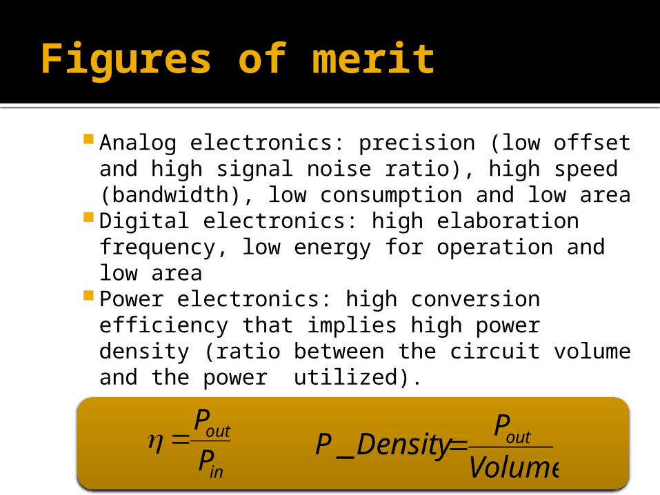
Power source
Specification: VI characteristic and type of source (AC/DC) Energy available (limited or unlimited)
Rules to utilize the source Safe operating area Rules on the type of load connected to the
source ex:▪ Maximum power point tracking requirement▪ Power factor correction requirement
Limit on the Instant power requirement EMI Rules
0),,( tIVf sourcesource
Power source example: Power distribution system
VI characteristic EMI rules
V
IOver current protection
Voltage reference

Power source examples: Batteries
The characteristic depends on charge level The quality of a battery on the ratio between
the charge stored and the volume For the rechargiable batteries another
important figure of merit is the number time cycles
Q dependent
RB
Q[mAh]
VbatVbat

Power source examples: AC line power source
The ac line power source requires a high power factor in order to have only current that gives a mean output power: No high order harmonics Current waveform proportional to the voltage
waveform
RB
t
Vac, Iac
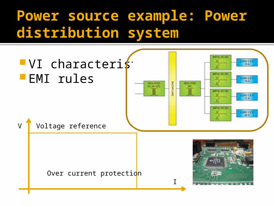
Power Load
Specification: Load specification Characteristic (Model)
▪ Static ▪ Dynamic
Rules to utilize the load Safe operating area Precision on current/voltage regulation EMI Rules: Maximum ripple
0),,( tIVg LOADLOAD
0),,( tIVh LOADLOAD
0),,(
0),,(
tIVh
tIVg
LOADLOAD
LOADLOAD

Power load examble: Battery charger
The charge current is equal to Ipre-ch when the battery is below 3V.
The battery is charged with Ich when the battery voltage is 4.1V > Vbatt >3 V.
After the charge goes in a control voltage charge phase in which the charge current depend on the error voltage Ich=K(4.2 – Vbatt)
Charge Profile for a Li-Ion battery
V
t
Battery Voltage
Battery Current
Q dependent
RBVbat
Model

Power load examble: WLED
Optical power of a LED is proportional to the current present on the device
The voltage in approximately constant
For the driving is used a pulsed current
Vd
Model
Rd
Id=Ifixed P(t) P(t) :

Power Load examples: uP power supply
Specication VRD 10.x per Intel P4 Prescott • Small voltage variation
• High current
• High slew rate
Output impedance resistive required
TYP,out DROOP loadV =VID - TOB - R I
“Droop Function” or “Adaptive Voltage Positioning”
Model Vcore
0),,( tIVh LOADLOAD
0),,( tIVg LOADLOAD

TransientSynchronous buck converters
DecouplingBulk
DC/DCConverter
Packaging Cdie
Processor
Max CPU Voltage
Min CPU Voltage
iC
iVRM
iC
iB iA
iAiB iVRM

VOUT
VMAX
Vmin
tΔV = ESR · ΔIOUT
Load current step variation
Output voltage response:
With Droop Function
VOUT
VMAX
Vmin
t
ΔV = ESR · ΔIOUT
Without Droop Function
CPU
CONTROLLORE
Feedback
L
COUT
ESR
VIN
I OUT
VOUT
Tolerance Band NOT respected Tolerance Band respected
IOUT
t
Power Load examples: uP power supply

The Power System
The total power system composed by the power circuits and the control circuits
meets the specifications of the power source and the power load
maximizes the power transfer.
PowerProcessing
Control Signal
SourceLoad
Power system
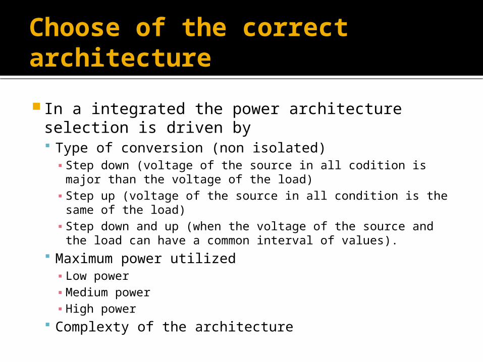
Choose of the correct architecture
In a integrated the power architecture selection is driven by Type of conversion (non isolated)
▪ Step down (voltage of the source in all codition is major than the voltage of the load)
▪ Step up (voltage of the source in all condition is the same of the load)
▪ Step down and up (when the voltage of the source and the load can have a common interval of values).
Maximum power utilized ▪ Low power▪ Medium power▪ High power
Complexty of the architecture

Determinate the maximum power
Dissipated power
Junction case resistace
Case Heater resistace
Heater Ambient resistace
The maximum power consumed by the system is limited by:
The package The cooling system

Choose the correct architecture
Dependely on the architecture the power related to the converter can be plotted as reported
Pload
Solution 1
Solution 2
Pload
Ploss
Solution 1
Solution 2
Ploss max

Linear conversion
This scheme, commonly used to stabilize low power supply, is designed to meet the load specification by using the analog strategies but it doesn’t maximizes the power transfer High power loss low efficiency low power density
in
out
inin
outout
in
out
V
V
VI
VI
P
P

Linear conversion efficienty
in
out
inin
outout
in
out
V
V
VI
VI
P
P
Pload
Bias consumption

Switched-mode conversion
To maximizes the energy transfer the power systems must be designed using energy storage elements (inductor and capacitor) and switches :
Capacitive (Charge Pump) Magnetic
Control & Sensing Signals
T h e r m a l E n e r g y

Capacitive Switch- mode conversion : Charge Pump
This scheme is the simpler Charge pump structure and its dynamic output voltage is
Without output current we have
The energy is periodically stored into and released from the E filed of the Pump or Flying capacitors. They are typically used in applications requiring relatively small amounts of current.
Reduced components Integration Example Voltage Step-Up

Capacitive Switch- mode conversion : Charge Pump
The voltage is reduced
With Ideal components the efficiency is
In case of load
ddpumpsw
out
VCf
I
41
The variable available to control the converter in the frequency

Capacitive Switch- mode conversion : Charge Pump (discrete)

Switched capacitor with MOS
Two phase charge Pump
If the RdsON is big the equivalent resistance is higher because during the turn on time the pump capacitor it isn’t completely charged.
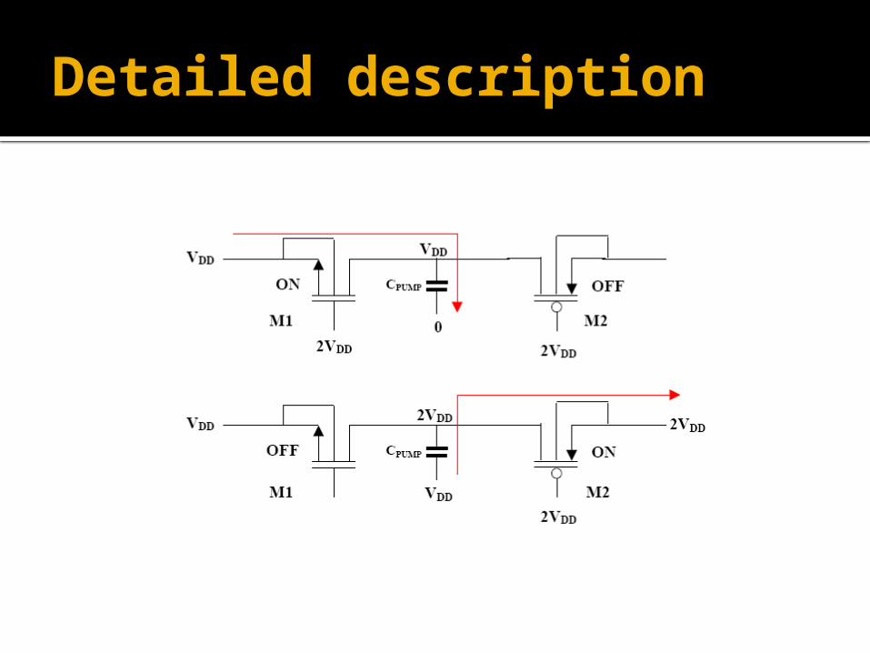
Detailed description
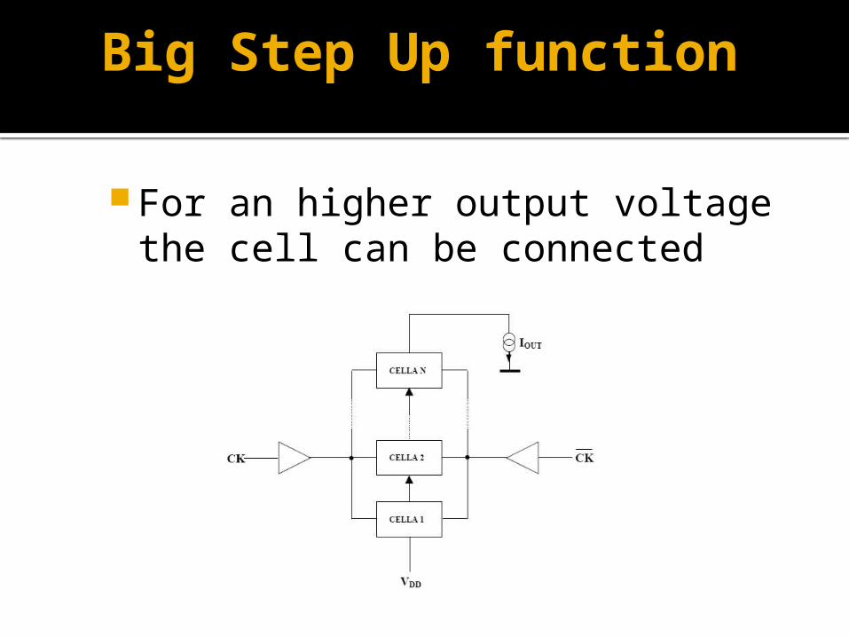
Big Step Up function
For an higher output voltage the cell can be connected

Charge pump control system
If the Charge pump is controlled it modulates its equivalent resistance in order to achieve the output voltage level. From an efficienty point of view it is equivalent to a LDO

Switch cap conversion efficienty
in
out
in
out
V
V
P
P
2
Pload
Bias consumption and turn on charge

Magnetic power conversion
This type of circuits are based on using the magnetic field to store the energy of inductor or transformer other than the electric field of the capacitors.
It’s possible classifying the converter on the basis of type source and load
AC-AC AC-DC Rectifier DC-AC Inverter DC-DC
presence or not of a transformer Non isolated Isolated
mode of operation DCM CCM
switching condition Hard switching Resonant

Type of converter
In general application IC integrated the different soultion utilized are
Step down
With the same voltage rate
Step up
L
Driver
Vin
PWM
Vout
L
Driver Driver
Vin Vout
PWM Not PWM
L
Driver
Vin
Vout
Not PWM

Switched-mode controlTo meet the load and source specification is
needed a control system : Voltage mode if the sensing signal is only the
voltage Current mode if in the sensed signal there is the
currentControl & Sensing Signals
T h e r m a l E n e r g y

Modulation
Each switch has two possible level so the control system can only modulate the duration of each state:
Frequency modulation• Ton constant• Toff constant• Duty constant
Fixed frequency• Pulse width modulation

Pulse width modulation at constant frequency
-
+
w
m
x
m = Constant
maxS
on
Wm
Tt
t
wmax
w
m
t
x
toffto
n
TS

Control loop
+
-
Vref
R1
C1
C2R2
C4
R4
R3
Vout
Vcomp
d Buck
1/Vosc Cntrl
vout
vref

Switched-mode controlTo meet the load and source specification is
needed a control system : Voltage mode if the sensing signal is only the
voltage Current mode if in the sensed signal there is the
currentControl & Sensing Signals
T h e r m a l E n e r g y
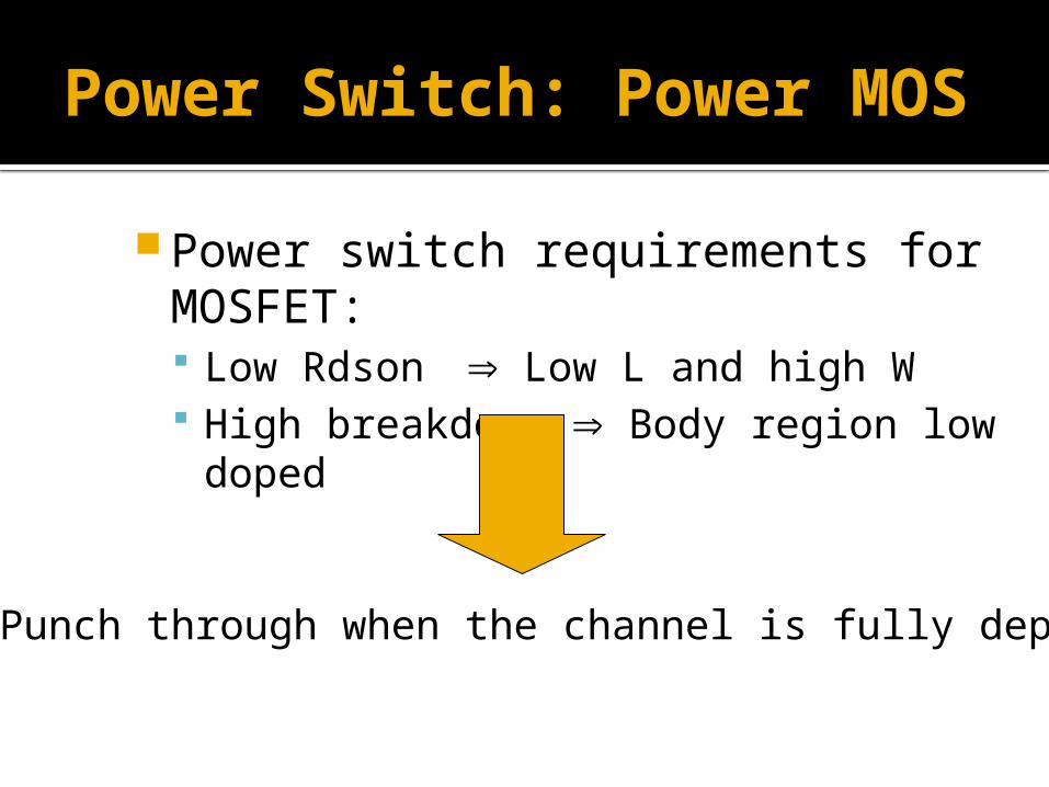
Power Switch: Power MOS
Power switch requirements for MOSFET: Low Rdson Low L and high W High breakdown Body region low
doped
Punch through when the channel is fully depleted

Power MOSFET
This structure has the high breakdown voltage and low Rdson: During the off state the depletion region is
present in the Nepi The Rds on decreases by reducing the
channel length
Vertical power MOS

Electromigration problem

Layout power MOSFET

Rdson contributions

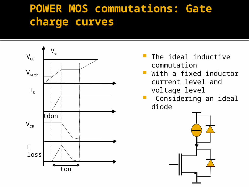
POWER MOS commutations: Gate charge curves
The MOS commutation characteristic with an inductive load is described by the gate charge curves
This curves is a charge controlled representation of the power MOS. They report the relation between the Vgs voltage and the charge injected in the gate to drive the device in relation with the switching condition (Ids, Vds)
Vgsth
Vd
Qg

POWER MOS commutations: Gate charge curves
The importance of the gate charge curves is related to the driving circuit design because they represent the relation between the driving mode and the switching losses.
The gate charge curves depends on the switching condition (Il ,Vds) and on the parasitic present on the application but almost they don’t depend on the driving circuit.
POWER MOS commutations: Gate charge curves
The ideal inductive commutation
With a fixed inductor current level and voltage level
Considering an ideal diode
ton
tdon
VGEth
VGE
VG
IC
VCE
Eloss

Gate charge in real condition
The parasitcs elements presents on the applications change the gate charge of the turn on and the turn off The capacitor of the Vds The diode reverse recovery The parasitc inductor Ls and Ld

Driving specification depending on gate charge
The driver ideal commutation can be calculated in the application considering the condition of maximum current but is a rare approssimation. The driver current depends on the impedance
The real commutation depend on the voltage hence the impedance present on the application that depend on many parameters: Ls that is vary important because it effects is
amplified by Lgate and Rgate limits the driving capabiity

Choose the correct architecture
Dependely on the architecture the power related to the converter can be plotted as reported
Pload
Bias and driving losses
Switching losses
Conduction losses
Increase the FOM= Qg Rdson
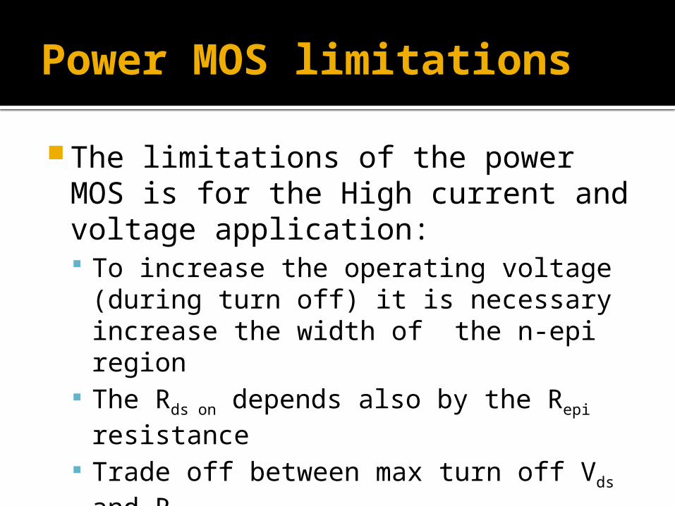
Power MOS limitations
The limitations of the power MOS is for the High current and voltage application: To increase the operating voltage (during
turn off) it is necessary increase the width of the n-epi region
The Rds on depends also by the Repi resistance
Trade off between max turn off Vds and Rds on

When does NPN turn on?
ION
ON
OFF
OFF
VM
I
OFF
OFF
VM
ION
OFF
ON
OFF
VM
Fly-BACK PHASE
A
B
1 2 3
1 2 3
A BA B A B
During phase 2 (high to low transition of A) both HSD and LSD are OFF due to the cross conduction control.
In this phase the inductor current flows through the intrinsic diode turning on the parasitic NPN.
OFF
ON
Ic P subNw
ell

Parasitic NPN negative fly back phase
Id
I npn
The Collector current flows from other pockets close to the Power.
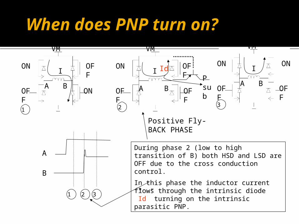
When does PNP turn on?
ION
ON
OFF
OFF
VM
ION
OFF
OFF
OFF
VM
ION
OFF
ON
OFF
VM
Positive Fly-BACK PHASE
A
B
1 2 3
1 2 3
A B A BA B
During phase 2 (low to high transition of B) both HSD and LSD are OFF due to the cross conduction control.
In this phase the inductor current flows through the intrinsic diode ”Id” turning on the intrinsic parasitic PNP.
IdP sub

Parasitic PNP positive fly back phase
The PNP Collector current flows into the substrate rising its voltage
N+N+N+N+ P+
pbody
nwellTriple well
Pwell
Parasitic PNP
Ipnp
Id

“Bootstrap” Supply for High-Side Power
+15V
uPDSP
orControl
IC
VDD
+15V
VDD
REG
Bias Power Supply
+DC Bus
Common (-DC Bus)
Bootstrap Diode
BootstrapCapacitor
PeakCurrentLimitingResistor

Bootstrap Cap Charges When Lo-Side ON
+15V
uPDSP
orControl
IC
VDD
+15V
VDD
REG
Bias Power Supply
+DC Bus
Common (-DC Bus)
0V
15V
Low-Side OnCharges Bootstrap
Capacitor
High-Sideis Off

Cap Supplies Power When Hi-Side ON
+15V
uPDSP
orControl
IC
VDD
+15V
VDD
REG
Bias Power Supply
+DC Bus
Common (-DC Bus)
BUS DC
15VBUS DC
Low-Sideis OFF
High-Sideis ON
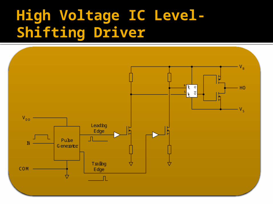
High Voltage IC Level-Shifting Driver
VB
VS
R
S
Q
Q
PulseGenerator
LeadingEdge
TrailingEdge
IN
HO
VDD
COM

HVIC Block Diagram for Half-Bridge Driver
HVLEVELSHIFT
LEVELSHIFT
VB
HO
VS
VCC
LO
COM
HIN
LIN
(VSS)

Junction Isolated CMOS HVIC Driver
p-n+
p+
n+
n+ n+ n+ n+
n+ n+ n+ n+p+
p+
p+
p-n+p- p-
p- p-
n-epi
n-epi
n-epi p-well
p-well
p-sub
p-sub
p-sub
P++P++
P++
P++
P++
P++
LDMOS LEVEL SHIFT
HV-FLOATING CMOSHVHV
HV
LV LVGROUNDED CMOS
Boot Phase

Substrate coupling
Transfer functions of the substrate coupling

Substrate coupling
R2=0.1
R2=0.5
R2=1

Conclusions
Voltage Conversion topologies (LDO, Switched cap,SMPS)
Power devices
Design problems


![Untitled Document [] · CS4299 3 4.10 Stereo Analog Mixer Input Gain Registers (Index 10h - 18h) .....24 4.11 Input Mux Select Register (Index 1Ah) .....25](https://img.pdfslide.us/doc/110x75/5acee6f77f8b9a8b1e8c0c5d/untitled-document-3-410-stereo-analog-mixer-input-gain-registers-index-10h.jpg)