Embed Size (px)
Citation preview

r
r
SSC ORATORY LIBRARY JUN 2 9 1992
GEM TN-92-93 UCRL-ID-108489
Muon Drift Chamber Physics and Engineering R&D Activities for the L* and GEM Detectors in FY 1991
E. Ables, R.M. Bionta, H.C. Britt, M. Capell, A.K. Chargin, G.A. Deis, O.D. Fackler, C.V. Johnson, III, M.E. Lowry, D.M. Makowieck.i, D.A.
Masquelier, K. McCammon, C.F. McConaghy, H.E. Olson, E.H. Schmitt, K.M. Skulina, R.L. Vital, T. Wenaus, and C.R. Wuest
September 25, 1991
Abstract:
This paper will describe the work canied out at LLNL on muon chamber R&D for the L* detector in FY 1991. Because of the L* proposal rejection in May, 1991, and the subsequent restructuring to form the GEM detector collaboration in July, 1991, the work described in this paper will also be seen to be applicable to the envisioned muon chamber subsystem for GEM.

UCRL-ID-108489 PREPRINT
Muon Drift Chamber Physics and Engineering R&D Activities
for the L * and GEM Detectors in FY 1991
E. Ables, R. M. Bionta, H. C. Britt, M. Capell, A. K. Chargin, G. A. Deis, 0. D. Fackler, C. V. Johnson, III, M. E. Lowry,
D. M. Makowiecki, D. A. Masquelier, K. McCammon, C. F. McConaghy, H. E. Olson, E. H. Schmitt, K. M. Skulina,
R. L. Vital, T. Wenaus, and C.R. Wuest
September 25, 1991
Thil it a preprint of a paper intended for publication in a journal or proceedings. Since cMngn may be made before publication~ this preprint is made available with the understanding that it will not be cited or reproduced without the permission of the author.
This work performed under the auspices of the U.S. oe.,.rtment of Energy by the Lawrmce Livermore National Laboratory under Contract W·740S.£NC-48.
DISCLAIMER
This document was prepared as an acccount of work sponsored by an agency of the United States Government. Neither the United States Government nor the University of California nor any of their employees, makes any warranty. express or implied, or assumes any legal liability or responsibility for the accuracy, completeness. or usefulness of any information, apparatus, product, or process disclosed, or represents that its use wouJd not infringe privately own rights. Reference herein to any specific commercial products. process, or service by trade name, trademark, manufacturer, or otherwise, does not necessarily constitute or imply its endorsement, recommendation, or favoring by the United States Government or the University of California. The views and opinions of authors expressed herein do not necessarily state or reflect those of the United States Government or the University of California. and shaH not be used for advertising or product endorsement purposes.
This report has been reproduced directly from the best available copy.
Available to DOE and DOE contractors from the Office of Scientific and Tec:hnicaI Information
P.O. Box 62. Oak Ridge, TN 37831 Prices available from (615) 576-8401, FrS 626-8401
Available to the public from the National Technical Information Service
US. Department of Commerce 5285 Port Royal Rd.,
Springfield, VA 22161
-
-• -
-..
-..
-
-..
•

Muon Drift Chamber Physics and Engineering R&D Activities for the L* and GEM Detectors in FY 1991
E. Ables, R. M. Bionta, H. C. Britt, M. Capell, A. K. Chargin, G. A. Deis, 0. D. Fackler, C. V. Johnson, III, M. E. Lowry,
D. M. Makowiecki, D. A. Masquelier, K. McCammon, C. F. Mcconaghy, H. E. Olson, E. H. Schmitt, K. M. Skulina,
R. L. Vital, T. Wenaus, and C. R. Wuest
Lawrence Livermore National Laboratory
Introduction
Lawrence Livermore National Laboratory (LLNL) joined the multi-national L * Detector collaboration in early 1990. The L * Detector has been described in great detail in a number of documents submitted to the Superconducting Super Collider (SSC) Laboratory.1.2
LLNL's participation in the L * collaboration consisted of a multi-disciplinary effon involving a number of physicists, engineers and technologists from different areas of the laboratory who came together to identify areas of research, development and engineering on the L* Detector where LLNL's expenise and technological capabilities could best be utilized.
Among these capabilities, superconducting magnet technology, chemistry and materials science, and design of new types of physics detectors were deemed areas of LLNL expertise best suited to the R&D effon needed for L *.
With the encouragement of the L* collaboration and the suppon of the Laboratory Director, LLNL became involved in a number of physics R&D and engineering tasks.3.4 These included:
1. Engineering and cost modeling of the superconducting magnet system for L * 2. Comparison of the cost of the superconducting magnet/muon system with the nor
mal magnet/muon system 3. Participation in the civil engineering of the L * detector experimental hall. 4. Collaboration on the R&D of liquid scintillator detectors for the L* hadron
calorimeter.5 5. R&D on electro-optics for the L * detector.6,7 6. Collaboration with the L3 group at CERN on an effon to pon data analysis and
event simulation computer codes to a massively parallel computer system at LLNL. 7. Collaboration with the L3 group on muon drift chamber R&D for the L * muon
chamber sub-system.
This paper will describe the work carried out at LLNL on muon chamber R&D for the L * detector in FY 1991. Because of the L * proposal rejection in May, 1991, and the subsequent restructuring to form the GEM detector collaborations in July, 1991, the work described in this paper will also be seen to be applicable to the envisioned muon chamber subsystem for GEM.
Muon Drift Chambers in L* and GEM
Muon drift chambers form the outer-most layers of the multi-layer L * and GEM detectors and are used to accurately identify and track events of interest resulting from the collisions of high energy protons in the Superconducting Super Collider. Interesting events (i.e. events with high physics content, or discovery potential) are typically characterized by the annihilation of the protons with resulting high energy gammas, electrons, muons, and hadron jets with high transverse momenta. For example, the reaction, Higgs --> ZZ* --> e+e-µ.+µ.-, leads to two electromagnetic showers and two penetrating muons. Where the Higgs boson is a never-before-seen neutral particle predicted, along with the already discovered W-:t and zo, by the standard model of Quantum Chromodynamics.
Muon identification is crucial in providing a prompt (level l) trigger for interesting events. The muon chamber sub-system is therefore envisioned as a multi-function system, with high-speed/coarse-position measuring nigger chambers complementing slower, highly accurate tracking drift chambers.
These chambers are immersed in a 0.8 Tesla magnetic field to provide measurement of muon charge and momenta. The chambers envisioned for L* were very accurately placed gas-filled multi-wire drift chambers based on the L3 muon drift chambers, with a trackposition resolution approaching 50 microns for 50 - 100 GeV muons.9
In the GEM detector, a number of different technologies have been proposed for the muon chamber sub-system. Among these are cylindrical drift tubes (DTs), square limited streamer tubes (LSTs), inductively coupled pad chambers (pads), resistive plate chambers (RPCs), transition radiation detectors (TRDs) (for the forward/backward chambers), and L •-style multi-wire drift chambers.
All these chambers have cenain features in common: operation using fine (25-50 micron diameter) anode and/or cathode wires, operation using a mixtures of gases typically containing a large percentage of argon with a smaller percentage of organic gas such as isobutane, and, in the case of wire-based chambers such as DTs, LSTs, and L* chambers, registration of a muon traversal in the form of a charge pulse collected on the anode wire and read-out by a pre-amplifier.
Muon Chamber R&D Performed at LLNL in FY 1991
LLNL hosted a 3 day L • Muon Chamber sub-system workshop in August, 1990. The workshop was intended to bring the L* Muon Chamber collaborators together at LLNL to present LLNL's technological capabilities and to familiarize LLNL physicists, engineers and technologists with the current state-of-the-an as implemented in the L3 Detector at CERN. The agenda from the workshop is given in Appendix A.
As a result of this workshop, a number of significant technology issues were identified as suitable for LLNL to work on. These included:
I. Study of wire failures in L3 muon drift chambers. 2. Study of new methods of bonding wires in planes and mass production of wire
planes. 3. Study of current state-of-the-art electronic pre-amplifiers for wire chamber read-out 4. Application of electro-optics to the read-out of wire chambers.
-
-
-
-
-
--
-..

5. Study of containment of wires without tension in low density silica aerogel.
A program to address the above issues was begun at LLNL using an internal grant from the Laboratory's Institutional Research and Development (IR&D) program through the Physics Department.
LLNL Muon Drift Chamber Test Bed
In order to carry out Items 1-3, we set out to design and build a small L3-style muon drift chamber as a test bed for muon chamber physics and engineering R&D. LLNL was charged by the L* Muon Chamber group with the task of designing, constructing and operating a full scale model of the proposed L * Muon Drift Chamber. The task was identified as an important exercise to bring LLNL engineers, and technicians up to speed on drift chamber technology as implemented at the L3 detector at CERN in Geneva.
In addition, the program was set up to identify new technologies which could be incorporated into the drift chamber design to make them more reliable, as well as cheaper and easily mass-produced. Also, coordination of tasks with the Mechanical Engineering Department was necessary to implement our R&D findings into plans for a drift chamber fabrication machine prototype that was built early in 1991.
As previously mentioned, the prototype chamber was patterned after the L3 method of chamber construction, and certain modifications were incorporated into the design where appropriate. For example, finely machined ceramic straight-edges and comb sttuctures were designed and fabricated for the precision localization of the wires in the wire-planes with an accuracy of about 10 microns.
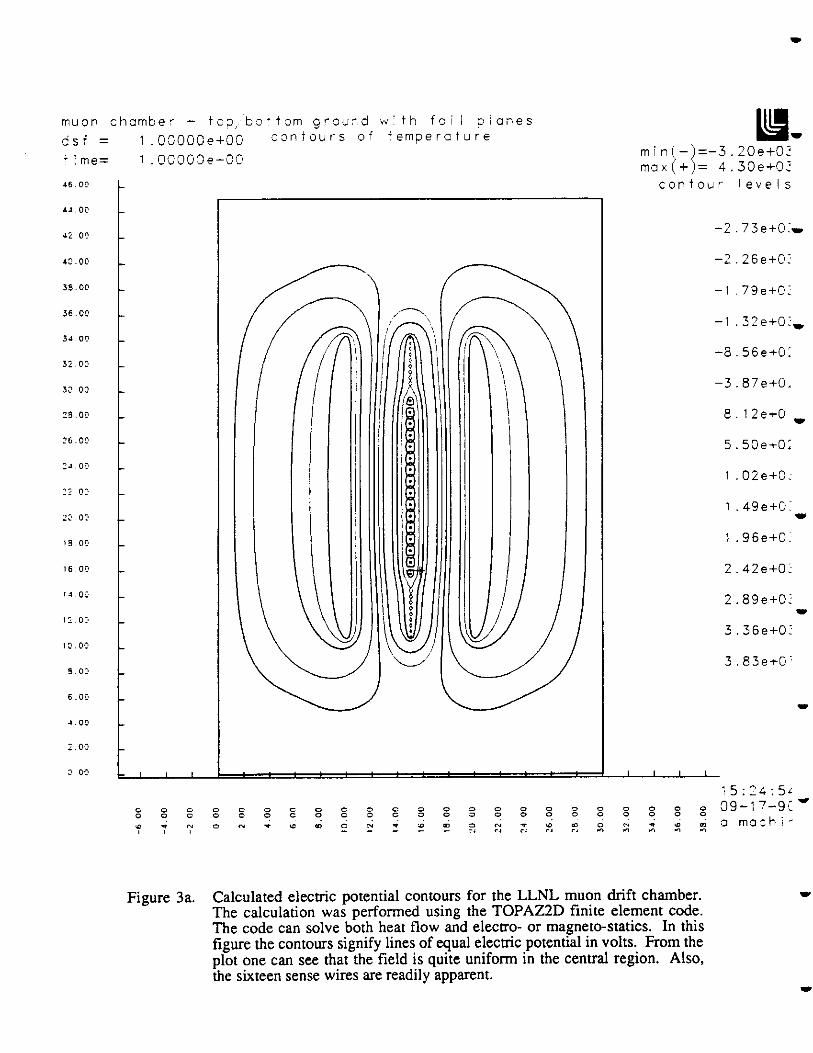
Figure 1 shows a photograph of the completed drift chamber. A schematic of the chamber cross-section is shown in Figure 2 and an electrostatic field map of the chamber calculated using the TOPAZ2D finite element codelO is given in Figures 3a-b. The drift chamber consists of a single central plane of 16 sense (anode) wires, 25 microns in diameter alternating with field shaping wires, 50 microns in diameter. The central plane is located between cathode (mesh) planes consisting of 50 micron diameter wires. Wires in each plane are separated by 4.5 mm and planes are separated by 5 cm. The entire set of planes is mounted on a rigid steel frame and placed in a gas tight box with upper and lower scintillation paddles for tagging cosmic ray muons. The overall length of the planes is 1 meter.
We successfully operated the drift chamber with LeCroy Research System's high density drift chamber electronics modules (model 2735DC 16 channel pre-amplifier/discriminator card) and, in addition, we worked with LeCroy engineers to modify their design, resulting in more stable operation of these cards for use with our drift chamber.
Wire Bond Failure
One of the problems associated with drift chambers is the occasional failure of a wire in the drift chamber leading to shorting of adjacent wires and poor chamber operation. The wires in drift chambers are typically gold-plated tungsten of 20-50 micron diameter, attached to printed circuit cards by epoxies or solders. The wire fails, typically by pulling out of its .solder joint.

In the process of constructing this drift chamber, we gained first-hand knowledge of the previously observed L3 experience of wire slippage out of the printed circuit cards. A small number of wires failed in our chamber as well. In order to better understand the failure mechanism, a detailed program of wire bonding and failure analysis was initiated.
We again observed wire failure as part of this program of study involving attachments of samples of tungsten wires to PC boards. The failed wire was a gold-plated tungsten wire attached with a 60% tin/40% lead solder, which was the standard way of attaching wires in the L3 muon chamber system. Also, other bonds were studied, including laser bonds using gold/tin, silver epoxies, indium solders, and lead/tin solders.
We utilized a number of analytical tools available at LLNL to determine the cause of the wire failure, among these were Auger electron beam microprobes, energy dispersive spectroscopy and high power optical and electron microscopy. A paper describing this work is in final draft form for submission to Nuclear Instruments and Methods in Physics Research (NIM) and is included in Appendix B.
The conclusions are that lead/tin solders are not appropriate for attaching gold-coated tungsten wires to PC boards due to the formation of a gold/tin eutectic and a depleted lead sheath around the tungsten wire leading to slippage of the now uncoated tungsten wire out of the solder bond. Over-heated solder joints are most likely to lead to this failure.
This work was presented in briefings to L3 physicists and engineers in meetings held at CERN in Geneva in January, 1991.
Alternative Wire Bonding Techniques
As previously mentioned, a number of different wire bonding techniques were studied. These included bonding agents such as conducting epoxies, indium/tin solders, tin/lead/silver solders, and gold/tin solders. Bonding techniques included standard soldering irons, high-temperature soldering irons, laser welding, and electric spot welding.
Figures 4 - 8 show cross sectional photomicrographs of some different bonding techniques. Of the different techniques, gold/tin solders appear to offer the best bond in terms of strength (high shear strength compared to lead based solders), and chemical integrity (no gold leaching of the gold-coated tungsten wire). In addition, we were able to demonstrate that the tungsten wire does not need to be coated with gold in order to be bonded to a PC board with gold/tin solder. The cost savings achieved by using uncoated tungsten wire is somewhat offset by the cost of the gold/tin solder compared to standard lead/tin solders. In addition, uncoated tungsten wire may not be suitable for long term operation in drift chambers, due to the build-up of oxides and other contaminants on the surface of the wire.
Laser bonding of wires was also successfully demonstrated for both 25, 50 and 75 micron diameter gold-coated and uncoated tungsten wires. Laser bonding is attractive for mass production techniques since the process can be carefully controlled, leading to highly reliable solder joints. Two- and three-axis soldering robots are also highly developed in the electronics industry and could be adapted to the production of wire planes.
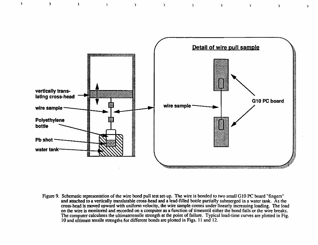
Alternative wire bonds were tested for ultimate tensile strength along with the more standard bonds. Figure 9 shows the test set-up for making these strength measurements. 25 and 50 micron wires were attached to small printed circuit board "fingers" using the various bonding techniques described above. These test samples were then mounted on a tensilometer as shown in the figure. One end of the wire and its PC board was attached to
...
..
..
..
..
..
-..
...
...
-
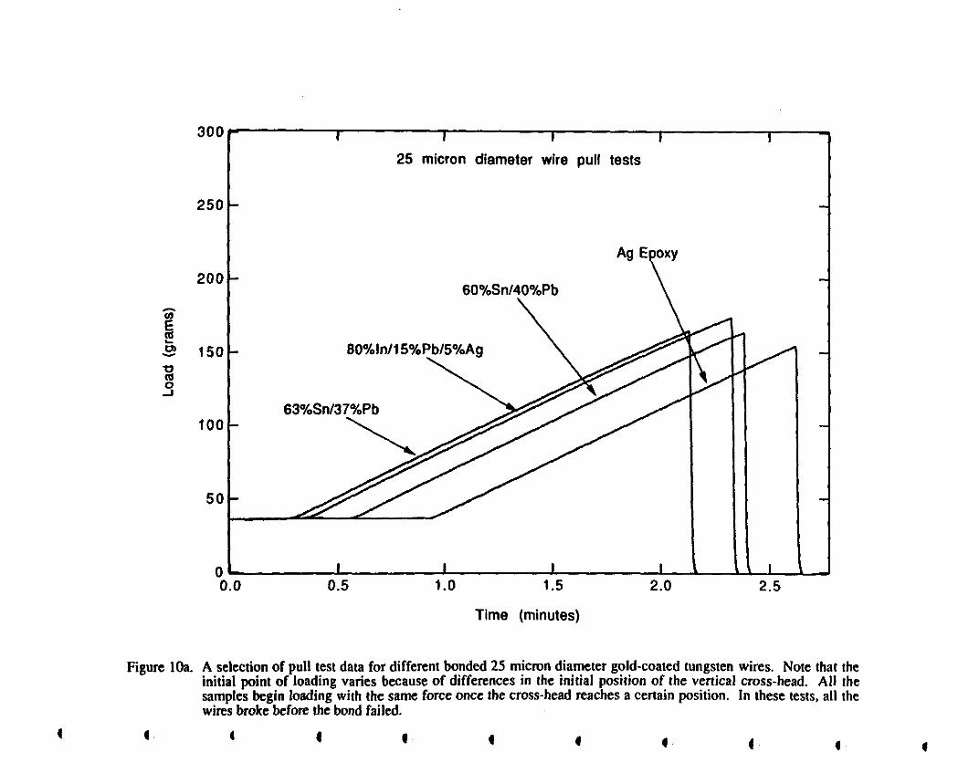
a swivel joint on a vertically translatable cross-head. The other end of the wire with its PC board was attached to a swivel joint connected to a bottle partially filled with lead shot and partially submerged in a tank of water. In a standard test, the cross-head would move vertically upward at a (adjustable) fixed velocity, slowly pulling the wire sample and the leadfilled bottle up. As the lead-filled bottle pulled out of the water, the load on the wire sample would increase linearly with time (or displacement). The load on the sample would be measured as a function of time until the sample failed. A computer recorded the load and time data and plotted the results. Figures lOa-b shows a few typical load curves. Typically, the wire sample would break before a bond would fail, although, as indicated earlier a lead/tin solder bond was observed to pull apart during one of these measurements. In addition, a silver-loaded epoxy bond was also observed to fail. This is shown in Figure IO.
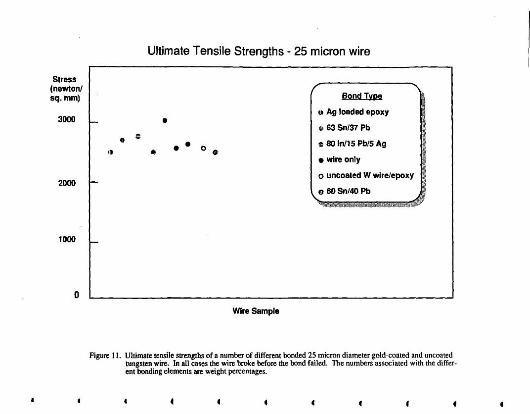
Figures 11 and 12 show results for a number of 25 and 50 micron wire pull tests. The results are plotted for the different wire bonds studied. Of the tests earned out, only two bonds were observed to fail. These tests do not indicate the effects of aging and other factors such as creep. Accelerated aging and creep tests would have to be earned out in order to fully understand the ultimate integrity of any of the bonding techniques studied.
Mass Production Techniques for Wire Planes
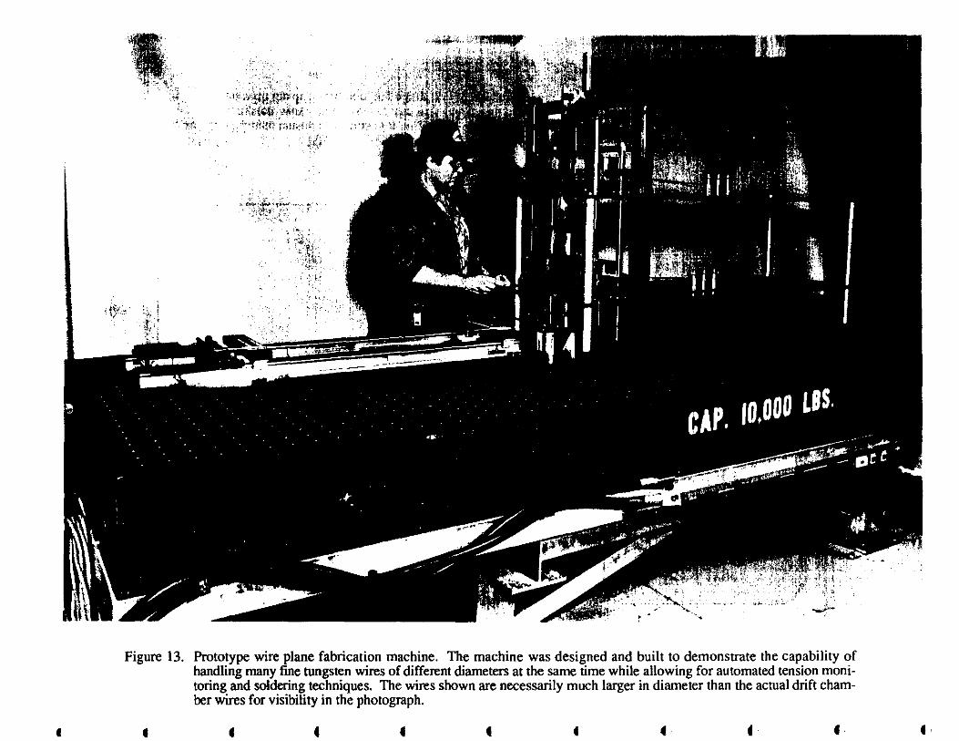
LLNL engineers, working in parallel with the physicists in the R&D program, have designed and fabricated a prototype wire plane manufacturing machine. This machine is shown in Figure 13. The machine is capable of fabricating planes of the required number of wires by feeding the wires on spools through a system of weighted pulleys. The weights are accurately machined pieces of lead and provide a constant tension of the wire of the correct amount necessary to limit gravitational sag and deflections due to electrostatic forces in the completed wire plane.
The plane is fabricated by attaching the wires to the printed circuit card using automated bonding techniques as previously discussed. The card and wires are then translated by the correct amount of length and the wires are soldered to the second printed circuit card along with the first printed circuit card for the next plane to be fabricated. At this point the first completed plane of wires and cards can be separated from the next plane of wires and so on. The completed plane of wires can be closely monitored at all times during this process to insure accurate tensioning, correct placement, etc. In addition, methods of plane fabrication utilizing frames or cassettes have been studied so that the completed wire plane is never allowed to be released from tension. These frames aid in the handling, assembly and precision alignment of wire planes into large arrays of planes for the final chamber.
Silica Aerogel R&D for Wire Bonding
In a related program, the wire bond failure issue was side-stepped completely by utilizing a method of mounting fine tungsten wires in a light-weight, porous silica aerogel material. This method would allow the wire to be positioned without tension and, as an added benefit, keep the wire in place in the event of a breakage.11 .
This idea was developed in collaboration with the LLNL Chemistry and Materials Science Department. As a first effort a single 50 micron gold plated tungsten wire was
mounted in the center of a 1 cm diameter cylinder of 150 mg/cm3 open-pore aerogel. The aerogel cylinder was surrounded by a gold foil and the entire assembly was placed in a gas of 90% argon and 10% methane (PIO gas) at one atmosphere. Figure 14 shows a schematic of the aerogel counter, which, in this configuration, operates as a cylindrical ionization counter. Figure 15 shows a photograph of the signal obtained from this detector from a gamma ray source. Figure 16 shows the detector count rate as a function of voltage for both source-in and source-out conditions.
Monte Carlo studies of the aero gel counter have been performed using the CYL TRAN electron-gamma shower code.12 In general, the presence of the aerogel adversely affects the integrity of the drifting electrons and so it is thought that aerogel is not a good candidate for a large volume drift chamber such as the L* chamber where electrons must drift over many centimeters. However, in applications such as small diameter drift tubes or ionization counters operating in the Geiger-Muller mode, aerogel counters might offer a solution for ruggedized radiation detectors. LLNL is pursuing this through its Technology Transfer Initiatives Office and the petroleum industry has shown interest in this work.
Read-out of Muon Drift Chamber Signals using Electro-optic Modulators
Another part of our drift chamber R&D study was to couple our model chamber to state-of-the-art Mach-Z.ehnder electro-optic interferometers in order to convert the charge collected on the drift chamber sense wires into optical signals proportional to the charge. The Mach-Z.ehnder modulator is described in detail in Appendices C through E.
We coupled a Mach-Z.ehnder modulator to a sense wire of our drift chamber and successfully read out the charge on the wire due to ionization tracks generated by Comptonscattered electrons in PIO gas from cobalt-60 gamma rays. This work is the first time an ionization chamber sense wire has been read out without standard electronic pre-amplification, and demonsuates that the Mach-Z.ehnder modulator has an adequate sensitivity to the direct charge accumulated on the sense wires due to the gas gain alone (about 106, in this experiment, or about 0.1 picoCoulomb ). This result could be of major importance to the experimental high energy physics community, especially with regard to large detectors such as L * or GEM, where tens of thousands of channels of electronics will be needed to read out various ionization chambers and charge sensitive detectors. The major issue which needs to be solved before wide-spread use is possible is the present high cost of these devices. Appendix E contains more details on this work and has been submitted to NIM for publication.13
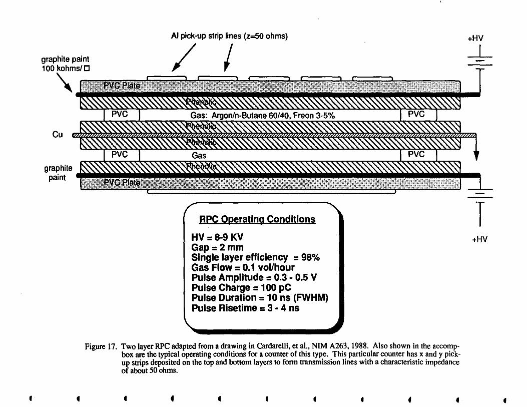
Resistive Plate Counter R&D for the GEM Trigger
Resistive Plate Counters (RPCs) are proposed as a means of providing a prompt trigger to the GEM detector. Figure 17 shows a schematic of an RPC designed for a large cosmic ray experiment along with its typical operating parameters.14 LLNL has proposed to perform R&D on RPCs as part of the GEM Muon Chamber and Triggering and Data Acquisition sub-systems.15 This program will look into new materials for RPCs including resistive glasses and sputter-coated cermet resistive electr9(ies. Appendix E contains a copy of the LLNL proposal to the GEM collaboration for RPC R&D in FY 1992.
-
-..
..
..
---
-•

-
Conclusions and FY 1992 R&D for Muon Chambers for the GEM Detector
We believe that our FY 1991 R&D program for L* and GEM muon chamber physics and engineering R&D has been very productive. In particular, starting early in the year with little experimental experience in multi-wire drift chambers of the L3 variety, we successfully built and operated a prototype L * muon drift chamber. This chamber allowed us to become familiar with the physics and engineering of this particular style of multi-wire drift chamber. Among the results garnered from this effort were:
1. Identification of precision fabrication technologies for locating wires to 10 microns accuracy.
2. Characterization of one of the failure mechanisms responsible for highly tensioned gold-plated tungsten wires slipping out of lead/tin solder bonds.
3. Identification and characterization of alternative wire attachment methods for highly tensioned tungsten wires.
4. Identification of a bonding method for uncoated tungsten wires. 5. Study of automated bonding techniques utilizing infra-red lasers and soldering
robots. 6. Design and fabrication of a prototype wire plane manufacturing machine. 7. Design and fabrication of a new type of ionization counter using silica aerogel to
hold a fine wire in place without tension. 8. First observation of direct charge signals from drift chamber sense wires by the di
rect attachment of an electro-optical modulator to the sense wire.
In FY 1992, we plan to continue this work and focus more on GEM specific R&D associated with the chosen technology utilizing pressurized cylindrical drift tubes or L *-style multi-wire drift chambers.16 Our earlier work is entirely applicable to the current effort since either technology involves the attachment and precise localization of tens of thousands of fine wires. In addition, our electro-optics R&D has studied the operation of MachZehnder interferometers on cylindrical drift tubes as well as L * drift chambers and demonstrated competitive performance compared to standard L3 electronic pre-amplifiers for noise, energy resolution and timing, as well as operation in a B field and operation in high radiation environments.17
We plan to study the issue of wire aging by looking at the HRS drift chambers (pressurized stainless steel drift tubes).18,19 These chambers were operated at SLAC for about 5 years in the early 1980's and have been sitting idle for the past 5 years. We will move a section of drift chambers to LLNL in the fall of 1991 and begin measuring wire tensions as well as operating characteristics of these tubes (position resolution, noise, etc.) compared to that measured when the tubes were new.
We also plan to fabricate new Resistive Plate Counters and compare them with existing technology RPCs in collaboration with physicists from MIT. 20 Our work will specifically look at technologies suited to producing large quantities (many thousands of square meters will be needed) of reliable, uniform trigger counters.
Finally, we intend to study the application of high strength carbon or glass fiber composite tubes for use in pressurized drift tubes. These composite materials offer the benefit of high strength, and low Z, which is a desirable combination for drift tube arrays envi-
sioned for the GEM detector. The reduction of mass in the tube walls will help to reduce the amount of muon scattering, which is 20% of a radiation length for the currently planned stainless steel tubes. Preliminary studies indicate that a carbon fiber composite tube could be fabricated to withstand pressures up to 40 psi with about a factor of 10 safety factor using a wall thickness of 0.45 mm. This corresponds to an areal mass of about 7 .3 x I0-4 g/cm2 or about 90% of the areal mass of a 0.15 mm thick stainless steel tube. Thinner walls could be made with some reduction in safety factor. A 0.25 mm wall thickness tube would have an areal mass of about half that of a stainless steel tube. The issues for study in utilizing composite tubes include neutron absorption and proton recoil from hydrogenous materials in the carbon fiber/epoxy matrix, which is about 2% by weight, as well as methods for providing an electrically conducting inner surface in the tube.
References
1. Expression of Interest to the SSC Laboratory by the L * Collaboration, May, 1990.
2. Letter of Intent to the SSC Laboratory by the L * Collaboration, University of California, Lawrence Livermore National Laboratory Proposal UCRL-PROP-105750, December, 1990.
3. H. Akbari, et al., "Progress on the Research and Development Program to Continue the Development of Precision Instrumentation for the Study of Muons in the TeV Region with Second Year Request," submitted to the Superconducting Super Collider Laboratory, September, 1990, (unpublished).
4. H. C. Britt, et al., "SSC L* Experiment/CERN L3 Experiment, A Project Proposed for Continued Funding in the FY 1991 IR&D Program," presented to the LLNL IR&D Review Committee, July 18, 1990, (unpublished).
5. R. Bionta, et al., "Liquid Scintillator Calorimetry, A Research and Development Proposal," submitted to the Superconducting Super Collider Laboratory, September, 1990, (unpublished).
6. M. Lowry, et al., "An Electro-Optical Imaging Approach to the Prompt Signal Processing Problem of Mega-Channel SSC Detector Arrays," Lawrence Livennore National Laboratory Preprint UCRL-JC-105645, submitted to the Symposium on Detector Research and Development for the Superconducting Super Collider, Fort Worth, TX October 15-18, 1990.
7. M. Lowry, et al., "Electro-Optic Imaging InstrUmentation Development at Lawrence Livermore National Laboratory: Implications for SSC Instrumentation Development," Lawrence Livermore National Laboratory Preprint UCRL-JC-105646, submitted to the Symposium on Detector Research and Development for rhe Superconducting SuperCollider, Fon Wonh, TX October 15-18, 1990.
--
-
-...
--
-..

-
8. "An Expression of Interest to Construct a Major SSC Detector," Superconducting Super Collider Laboratory Document, SSC EOI-0020, July 8, 1991, (unpublished).
9. D. Antreasyan, et al, "The L3 High-resolution Muon Drift Chambers: Systematic Errors in Track Position Measurements," Nucl. Instr. Meth. A252, pps. 304-310, 1986.
10. A. Shapiro, "TOPAZ3D - A Three Dimensional Finite Element Hear Transfer Code," Lawrence Livermore National Laboratory Internal Document UCID-20484, August, 1985 (unpublished).
11. C. Wuest, et al., "Aerogel Ionization Counter," Lawrence Livermore National Laboratory Disclosure and Record of Invention, Case No. IL-8725, S-73, 911 (RL-11,434), April, 1991, (unpublished).
12. J. Halbleib and T. Melhorn, "ITS: The Integrated Tiger Series of Coupled Electron/Photon Monte Carlo Transport Codes," Sandia National Laboratory Document SAND 84-0573, November, 1984, (unpublished).
13. E. Ables, et al., "Observation of Drift Chamber Signals using a Mach-Zehnder Electro-optic Modulator," Lawrence Livermore National Laboratory Preprint UCRL-107396-REVI, submitted to Nuclear Instruments and Methods in Physics Research, May, 1991.
14. R. Cardarelli, et al., "Progress in Resistive Plate Counters," Nucl. Instr. Meth. A263, pps. 20-25, 1988.
15. C. Wuest, et al., "Resistive Plate Chambers for the GEM Detector: A Proposal for Research and Development," submitted to the Superconducting Super Collider Laboratory and the GEM Detector Collaboration, September, 1991, (unpublished).
16. H. C. Britt, et al., "GEM High Energy Physics at LLNL and SSC" presented to the LLNLLDRD Review Committee, August 15, 1991, (unpublished).
17. M. Lowry, et al., "Direct Charge Readout of Ionization Chamber Detectors using Electro-Optic Modulators without Electronics Preamplification," to be published.
18. D. Rubin, et al., "The Central Drift Chamber for the High Resolution Spectrometer at PEP," Nucl. Instr. Meth. A203, pps. 119-127, 1982.
19. S. Bhadra, et al., "The Design and Construction of the CDF Central Drift Tube Array," Nucl. Instr. Meth. A268, pps. 92-104, 1988.
20. I. Pless, "SSC R&D Proposal for the GEM Muon Detector System," September, 1991, (unpublished).

•
Figure 1. Muon drift chamber constructed at LLNL as a test bed for new technology studies. The box contains three planes of wires immersed in a gas of 90% argon, I 0% methane. Cosmic ray muon trigger paddles are placed on the top and bottom surfaces. The chamber is interfaced to a CAMAC data acquisition system and controlled by a VaxStation 3100 via SCSI bus.
• • • • • • • • • •

ril•---- 50mm
4.smm ' ~ --o
T~ 0 0 0 0 0 0 0 0 0
• Field Wires +1600 volts
_.i._ Sense Wires ..,... +2900 volts
Mesh Wires 0
·2400 volts
0 0 0 0 0 0 0 0 0 0 0 0 0 0 0 0 0 0 0 0 0 0 0 0 0 0 0
---" .. ..-.tl,.•t----50 mm ---t ... ~I
• 0 • 0 • 0 ... 0 • 0 ... 0 • 0 ... 0 • 0 ... 0 • 0 ... 0 • 0 ... 0 • 0 ... 0 • 0 ... 0 • 0 ... 0 • 0 ... 0 • 0 ... 0 • 0 ... 0 • 0 ... 0 • 0 ... 0 • 0 ... 0 • 0 ... 0 • 0 ... 0 • 0 ... 0 • 0 • 0 • 0
Figure 2. Cross section of LLNL muon drift chamber. The mesh and field wires are 50 micron gold-coated tungsten wire. The sense wires are 25 micron gold-coated tungsten wire.
-muon chamber - to?, bo·tom graurd w: th foi I planes LI. dsf = 1 .OOOOOe+OO contours of temperature
min\-)=-3.20e+O~ max ( +) = 4 . 3 0 e +O ~
contour levels
.. :me= 46.00
4.1.00
.i.:z 00
4:::· .oo
35.00
36.00
34 00
32.00
3~ 00
:?.9 .O•J
.'.'2 OC·
! 8 OC•
16 00
! 4. O·J
1::?. OC•
1 O O·J
6 .O•:·
4. 00
2.00
=· 00
1 . OOOOOe+OO
0 0 0 0 0 0 c 0 c 0 c 0 0 0 0 c 0 c 0 c 0 c ~ • N 0 • ~ m ~ N = ' ' '
0 0 0 0 0 0
~ ~ 0 .,
\ \ I
0 0
N N
0 0 0 0
• ~ "
0 0 0 0 0 0 0 0 0 0 0 0
m 0 N • ~ m '' ~ ~ ~ ~ ~
Figure 3a. Calculated electric potential contours for the LLNL muon drift chamber. The calculation was performed using the TOPAZ2D finite element code. The code can solve both heat flow and electro- or magneto-statics. In this figure the contours signify lines of equal electric potential in volts. From the plot one can see that the field is quite uniform in the central region. Also, the sixteen sense wires are readily apparent.
-2.73e+o~ ..
-2.26e+o:
-1. 79e+o:
-1 . 32e+o:.,
-8.56e+o:
-3.87e+O.
8.12e+O.,
5. 50e+o;
1 . 02e+O:
1 . 49e+O -1.96e+o:
2.42e+o:
2.89e+o: -3.36e+o:
3.83e+o•
-·, 5 24 5, 09-1 7-9C -a ma ch i .
-
-

muon chamber- - top,'bo;.tom grour.j v1itf-.
csf = 1.oooooe+OO 'ector p:oi of f o i I
f I L.< x: pianes
min(-)= 0. max(+)= 2.02e+03
vector !eve's
ti me=
44,00
4.:Z 00
40.00
35 00
34.00
32:. 00
::!5. OC·
:?6 00
:!C•. OC•
! B 00
16 OC•
1 ~·.QC·
5.00
6.0C·
4.0Q
2.00
1 . OOOOOe+OO
~ 0 0 0 0 0 0 0
IC ...,. "' 0
' ' '
0 0
N
..
0 0
•
... ............ .,
H111,,:i1i,i!i1 .. 1.1·11111: ·•·•
0 0 0 0 0 0 c 0 c 'C c 'C ~ m
= " ~ :<>
.:.::::::::·:;
0 0 0 0 0 0 0 0 0 0 0 0 " 0 0 0 0 0 0 0 0 0
m 0 N ~ ~ m 0 N • ~ m
" N " N " ~ ~ ~ ~ ~
Figure 3b. Calculated elecnic field vector plot for the LLNL muon drift chamber. The calculation was performed using the TOPAZ2D finite element code. In this figure the vectors signify the magnitude and direction of the elecnic field in volts/cm. From the plot one can see that the field is quite uniform in the central region. Also, the sixteen sense wires are readily apparent. Arrows point in the direction opposite to the drift electron's travel.
2.02e+03
1 . 51 e+03
1 . 01 e+03
5.04e+02
0.
2 : 8 -. -~
09-1 7~9c a ma ch i
•
• .... , · ...
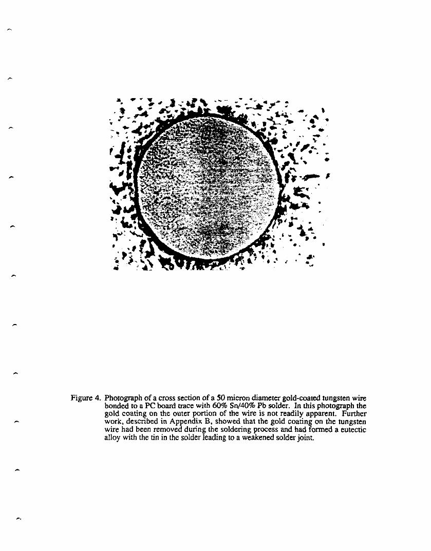
Figure 4. Photograph of a cross section of a 50 micron diameter gold-coated tungsten wire bonded to a PC board trace with 60% Sn/40% Pb solder. In this photograph the gold coating on the outer portion of the wire is not readily apparent. Further work, described in Appendix B, showed that the gold coating on the tungsten wire had been removed during the soldering process and had formed a eutectic alloy with the tin in the solder leading to a weakened solder joint.
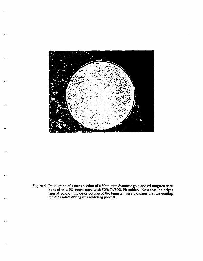
Figure 5. Photograph of a cross section of a 50 micron diameter gold-coated tungsten wire bonded to a PC board trace with 50% In/50% Pb solder. Note that the bright ring of gold on the outer portion of the tungsten wire indicates that the coating remains intact during this soldering process.
-
-
-
-
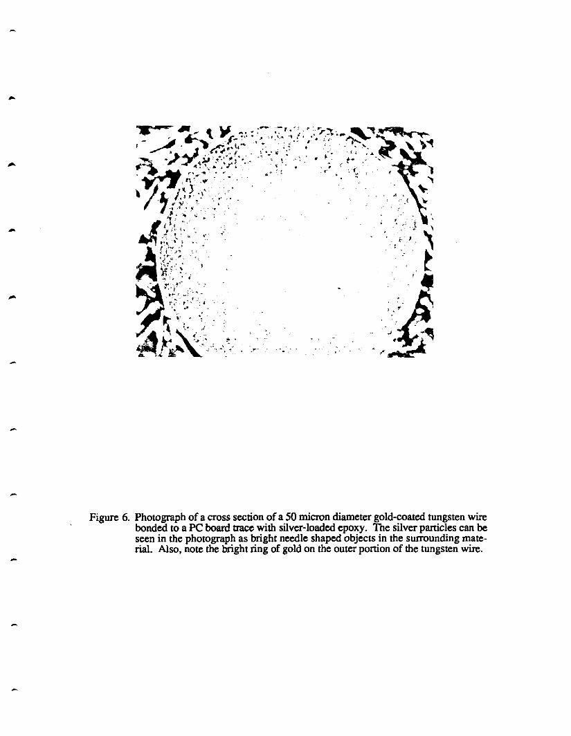
Figure 6. Photograph of a cross section of a 50 micron diameter gold-coated tungsten wire bonded to a PC board trace with silver-loaded epoxy. The silver particles can be seen in the photograph as bright needle shaped objects in the surrounding material. Also, note the bright ring of gold on the outer portion of the tungsten wire.

Figure 7. Photographs of tungsten wires bonded to a PC board traces with a Nd: Y AG laser using 80% Au/20% Sn solder. The upper photograph shows a series of bonds using 25 and 50 micron diameter uncoated and gold-coated tungsten wires. The lower photograph shows an enlargement of one of the laser-bonded 25 micron diameter uncoated tungsten wires. The scale in the upper photograph is in inches.
) ) ) ) ) ) ) ) )
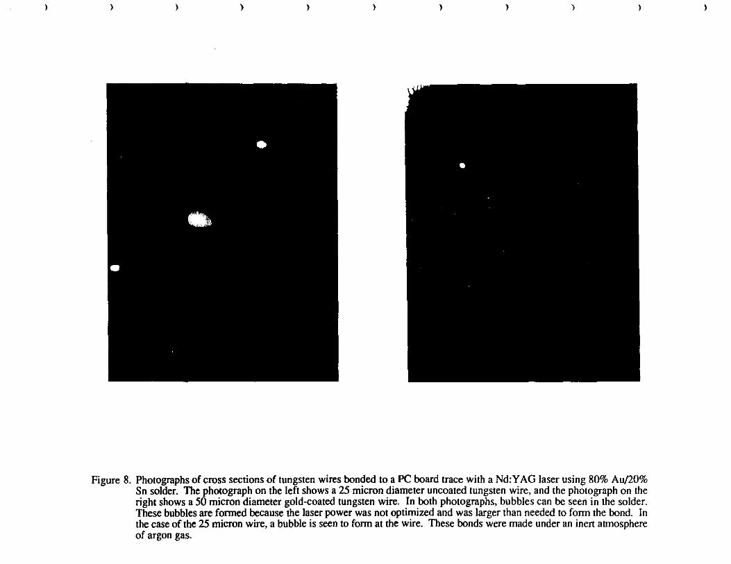
Figure 8. Photographs of cross sections of tungsten wires bonded to a PC board trace with a Nd: Y AG laser using 80% Au/20% Sn solder. The photograph on the left shows a 25 micron diameter uncoated tungsten wire, and the photograph on the right shows a 50 micron diameter gold-coated tungsten wire. In both photographs, bubbles can be seen in the solder. These bubbles are formed because the laser power was not optimized and was larger than needed to form the bond. In the case of the 25 micron wire, a bubble is seen to form at the wire. These bonds were made under an inert atmosphere of argon gas.
)
) )
vertically translating cross-head
)
wire sample----
Polyethylene bottle
Pb shot-----
water tank-----
) ) )
wire sample
) ) )
Detail of wire pull sample
""' ..._ /1DPCboanl I 'ij
~I 'l :~ ::~
:11
I! ·~ ~~::::
.x"'-"-°"'»"Mi$?A"<W;f,*""'"""'"""'"'''"""-«£;";WftW;",,_'"''''"'"ij@,,l,,
Figure 9. Schematic representation of the wire bond pull test set-up. The wire is bonded to two small G 10 PC board "fingers" and attached to a vertically translatable cross-head and a lead-filled bottle partially submerged in a water tank. As the cross-head is moved upward with uniform velocity, the wire sample comes under linearly increasing loading. The load on the wire is monitored and recorded on a computer as a function of timeuntil either the bond fails or the wire breaks. The computer calculates the ultimatetensile strength at the point of failure. Typical load-time curves are plotted in Fig. 10 and ultimate tensile strengths for different bonds are plotted in Figs. 11 and 12.
~
"' E al ~
DI ~
"O al 0 _,
Figure IOa.
c •
300,..-~~~~-r-~~~~,...-~~~~,...~~~~--r-~~~~-r~~ ......
25 micron diameter wire pull tests
250
200
150
. 63%Sn/37%Pb
100 I-~
I / 50
o,__~~~~-'-~~~~_,_~~~~-'-~~~~-'-~-'-~~--'"~-'--'
0.0 0.5 1.0 1.5 2.0 2.5
Time (minutes)
A selection of pull test data for different bonded 25 micron diameter gold-coated tungsten wires. Note that the initial point of loading varies because of differences in the initial position of the vertical cross-head. All the samples begin loading with the same force once the cross-head reaches a certain position. In these tests, all the wires broke before the bond failed.
• • ' ' • • f • f

)
-rn E .,, .... CJ --0 .,, 0 ..J
Figure !Ob.
) ) ) ) ) ) ) )
6001- SO micron diameter wire pull tests
60%Sn/40%Pb loaded
5001- /A~ // II
4oot-80%Sn/20%Au ~
300
2ool // r0%1n/15%\~~%Alll 60°//40%Pb
96%Sn/4%Ag
100· - - bond failure
o--~~~~ ........ ~~~~--'~~~~~....._~_....__~__..~~~~~ .... 0 2 4 6 8 10
Time (minutes)
A selection of pull test data for different bonded 50 micron diameter gold-coated tungsten wires. In the case of the laser bonded 80%Au/20%Sn, the tungsten wire is uncoated. In these tests, all the wires broke before the bond failed except the 96%Sn/4%Ag bonded wire. In this case the wire pulled out of bond. The test marked "60%Sn/40%Pb loaded" was a test in which a wire was suspended with a 300 gram static load for about 72 hours prior to the pull test. The difference in this test compared to the "unloaded" 60%Sn/40%Pb test is within the error of margin for these tests.
)
I
Stress (newton/ sq. mm)
3000
2000
1000
0
•
• ~
lffl
Ultimate Tensile Strengths - 25 micron wire
•
• •• 0 0
Wire Sample
Bond Type
"" Ag loaded epoxy
*' 63 Sn/37 Pb
@ 80 ln/15 Pb/5 Ag
•wire only
:~~
r1:
o uncoated W wire/epoxyj•~ o 60 Sn/40 Pb .J
~~filf.3J(::;~:~f@tf1#·
Figure 11. Ultimate tensile strengths of a number of different bonded 25 micron diameter gold-coated and uncoated tungsten wire. In all cases the wire broke before the bond failed. The numbers associated with the different bonding elements are weight percentages.
• ' • • • • ' • •

)
Stress (newton/ sq. mm)
3000
2000
1000
0
)
1111 ,,p
) ) ) ) ) )
Ultimate Tensile Strengths - 50 micron wire
wire pulled out of bond
L,. ·di> Ill> oftl .•~@~~~
••• 0 0 CDtD
00
Wire Sample
BondJype
"'' Ag loaded epoxy
* 63 Sn/37 Pb
e 80 ln/15 Pb/5 Ag
0 normal epoxy
• wire only
o bare W wire/epoxy
o 60 Sn/40 Pb
CD 80 Au/20 Sn
Figure 12. Ultimate tensile strengths of a number of different bonded 50 micron diameter gold-coated and uncoated tungsten wire. In two cases, the wire pulled out of the silver-loaded epoxy bond. The numbers associated with the different bonding elements are weight percentages.
) )
•
'\;''
;!l ·' ,i' ..
.,,, ''.;' '.\~!:'.·~:,,
' . ·~~~
i .•.
»• -..,:t~
'·::
":-.,. ,',' ~
·.11 <'_>iti~'g_r. ~"II 4 . .r."":r-, .
. :i~<l~· !!\Hi,· '.:-, ~..rt1if~- f:;ff;!-~ J'. :
~+~·t:::·:··· .. :J .. < -_, ' •!< .~ .. :_~.,-. ··:-'..1't1J
'::'•' . ,· .;.·i<
~ \ ( '
J.·~~ .. ;.i;,,,
,;·p·
.-1;; -f:.,..:,
Figure 13. Prototype wire plane fabrication machine. The machine was designed and built to demonstrate the capability of handling many fine tungsten wires of different diameters at the same time while allowing for automated tension monitoring and soldering techniques. The wires shown are necessarily much larger in diameter than the actual drift chamber wires for visibility in the photograph.
• • • • • • • f • .,

) )
to electronics
Figure 14.
) ) )
150 mg/cm3 silica aerogel
)
6cm
~ 2cm -.j
-HV
) )
75 µm Au foil
(Not to scale)
)
50 µm Au/W wire
1 cm
Cylindrical ionization counter made with open-pore, 150 mg/cm3 silica aero gel. A single 50 micron diameter gold-coated tungsten wire is contained in the center of the cylinder. The entire assembly is pumped out under vacuum for 24 hours prior to backfilling with 1 atmosphere of 90% argon, 10% methane (PlO) gas.
) )
•
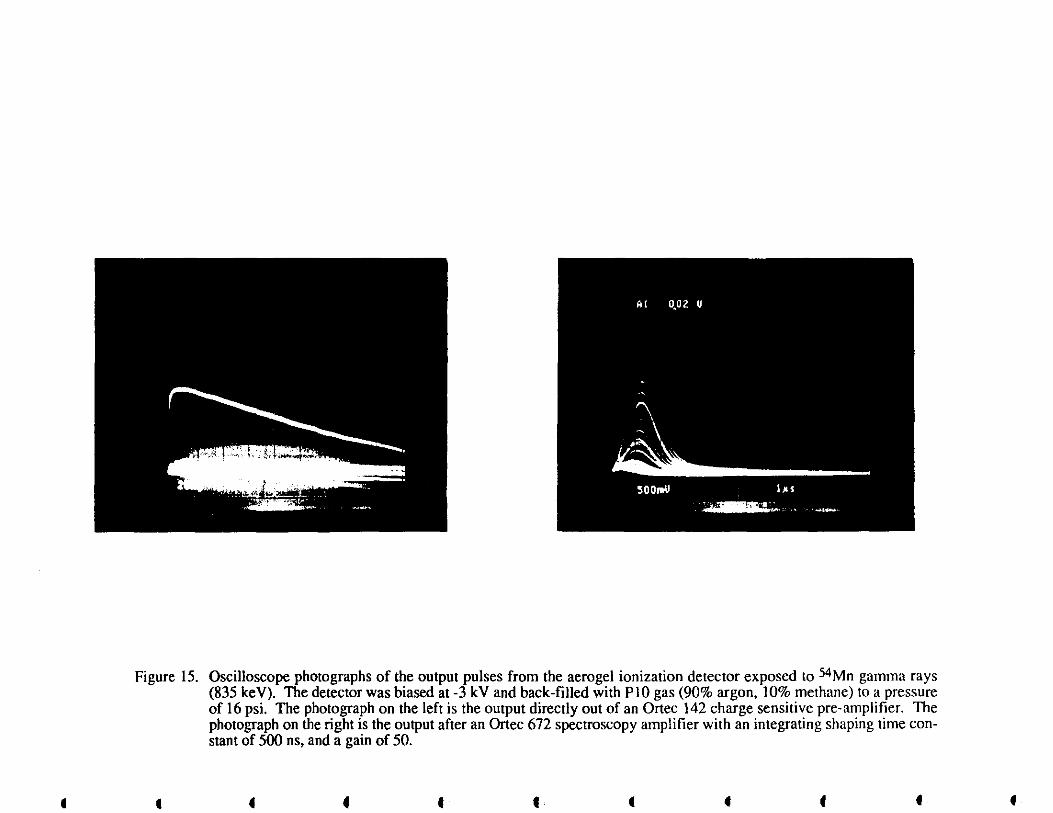
Figure 15. Oscilloscope photographs of the output pulses from the aerogel ionization detector exposed to 54Mn gamma rays (835 keV). The detector was biased at -3 kV and back-filled with PIO gas (90% argon, 10% methane) to a pressure of 16 psi. The photograph on the left is the output directly out of an Ortec 142 charge sensitive pre-amplifier. The photograph on the right is the output after an Ortec 672 spectroscopy amplifier with an integrating shaping time constant of 500 ns, and a gain of 50.
• • 4 • • • • f • •

} } }
1000
100
~
N ::r:: ~
CD 1ii 10 a: .. c ::J 0 0 .. 0 u 1 CD .. CD 0
0.1
0.01=-~~~-L~~~~-'-~~~~L-~~~-L~~~~-'-~~~~
Figure 16.
1.0 1.5 2.0 2.5 3.0 3.5 4.0
Detector Bias (kV)
Aerogel detector count rate versus detector bias between the outer cylindrical foil electrode and the inner 50 micron diameter gold-coated tungsten wire. The detector was placed about I cm from a 100 microCurie manganese-54 gamma ray source (835 ke V). The lower curve is the observed count rate with the source removed.
)
•
Al pick-up strip lines (z=50 ohms)
graphite paint 100 kohms/a / I
\
Cu
graphite paint
•
RPC Operating Conditions
HV: 8-9 KV Gap:2mm Single layer efficiency = 98°/o Gas Flow = 0.1 vol/hour Pulse Amplitude = 0.3 - 0.5 V Pulse Charge = 100 pC Pulse Duration = 1 O ns (FWHM) Pulse Risetime = 3 - 4 ns
Figure 17. Two layer RPC adapted from a drawing in Cardarelli, et al., NIM A263, 1988. Also shown in the accompbox are the typical operating conditions for a counter of this type. This particular counter has x and y pickup strips deposited on the top and bottom layers to form transmission Jines with a characteristic impedance of about 50 ohms .
• • • ' • • • •
+HV
_L
T +HV
•

,...
APPENDIX A
llNL L* MUON CHAMBER WORKSHOP
AGENDA AND LIST OF PARTIOPANTS

-
-
-
L* AGENDA
Muon Chamber Lawrence Livermore National
Aug. 29·31, 1990 {revised 8/31190)
Workshop Laboratory
Meetings to be held in T2925 Sakura Room
Wednesday. 29 August
8:30 Van Depans from hotel 9 :00 Badging at East Badge Office
9:45 10:15 10:45
Session 1 - Introduction
Welcome and Introduction to LLNL Engineering at LLNL Logistics
11 :00 Break
11: 15 SSCL Issues
12:15 Lunch (catered) lawn in front of 8194
Bruce Taner Tony Chargin Orrin Fackler
Mike Harris
Session 2 • Current Issues, Research, and Development
1:15 2:00 2:30
Overview of Muon Chamber Critical Issues Chamber Configuration Studies Chamber Design R&D
3 :00 Break
3:30 4:00 4:30 5:00
Alignment R&D {ETH) Suppon System Design (Draper) Status of Technical Information Center Discussions
6:00 Return to Hotel
Marion White Charles Grinnell Gerard Faber/Hans Postema
Gen Vienel Len Wilk Tom Shannon

-2-
AGENDA L* Muon Chamber Workshop
Lawrence Livermore National Laboratory Thursday. 30 August
8:30 Van Departs from hotel
Session 3 - Relevant R&D at LLNL
9:30 Initial R&D Plans & LLNL 10:00 Overview of Selec1ed LLNL Capabililies
10:45 Break
10:45 Alignment Techniques at LLNL 11 :30 Struc1ural Design and Analysis
12:15 Lunch (catered) Served in Lawn Area, Bl94
1 :15 2:30 3:15
NOVA Tour Composile Materials Silica Aerogel R&D for Muon Chambers
4:00 Break
4: 15 Advanced Electronics at LLNL 5:00 Electro-Optical Electronics
5:30 Dinner (Barbecue at LLNL swimming pool)
8:00 Van pie/cup for return to Hotel
Rich Bionta Gary Deis
Lee Griffilh Dale Schauer
Roben Turner Gordon Spellman Craig Wuest /Larry Hrubesh
Stefan Swierkowski Mark Lowry
-...
-
...
-...
-...
--
-
L*
-3-
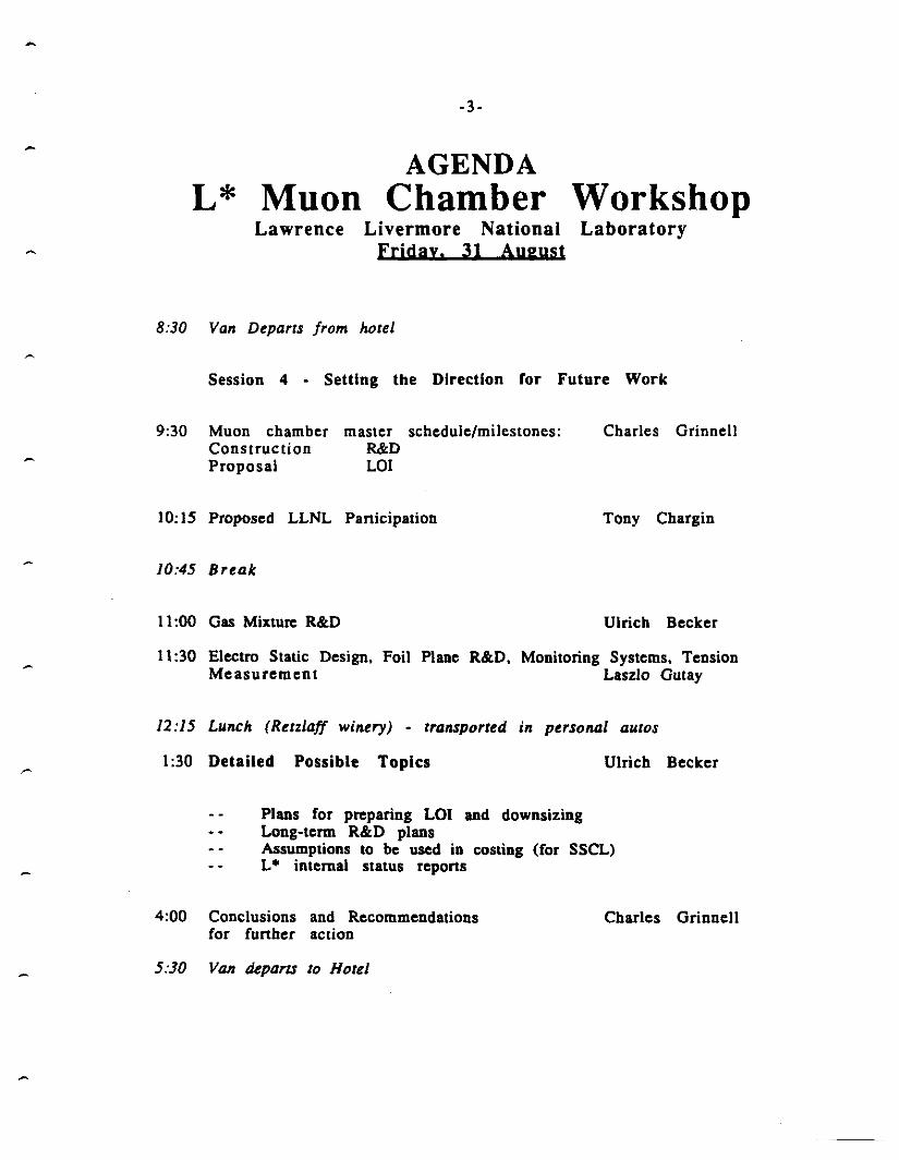
AGENDA Muon Chamber
Lawrence Livermore National Friday. 31 August
8:30 Van Departs from hotel
Workshop Laboratory
Session 4 - Setting the Direction for Future Work
9:30 Muon chamber Construction Proposal
master schedule/milestones: R&D LOI
10:15 Proposed LLNL Panicipation
10:45 Break
11 :00 Gas Mixture R&D
Charles Grinnell
Tony Chargin
Ulrich Becker
11 :30 Electro Static Design, Foil Plane R&D, Monitoring Systems, Tension Measurement Laszlo Gutay
12:15 Lunch (Retzlaff winery) - transported in personal autos
1 :30 Detailed Possible Topics
Plans for preparing LOI and downsizing Long-term R&D plans
Ulrich Becker
Assumptions to be used in costing (for SSCL) L • internal status repons
4:00 Conclusions and Recommendations for funher action
5:30 Van departs to Hotel
Charles Grinnell

L* MUON CHAMBER WORKSHOP PARTICIPANTS 8/29/90; MORNING SESSION
BECKER, ULRICH
BIONTA, RICHARD
BUJAY,ADAM
BURGER, JOSEPH
CALDERON, MANUEL
CAPELL, MIKE
CHARGIN, TONY
CHIPLEY, KEN
FABER, GERARD
GRIFFITH, LEE
GRINNELL, CHARLES
GUT A Y, LASLO
HARRIS, MIKE
HEIM, JOE
HORVATH, JOHN
JOHNSON, COLEMAN
KREISLER, MIKE
LOWRY, MARK
McCONAGHY, CHARLES
MUGGE, MARSHALL
NEEF, BILL
POSTEMA, WILLEM
SANGSTER, CRAIG
SCHAUER, DALE
SHANNON, TOM
STOEFFL, WOLFGANG
TATRO, CLEM
VIERTEL, GERT
WEST, CRAIG
WHITE, MARION
WILK, LEN
MIT
LLNL,ODIV.
PURDUE
MIT
LLNL/ME
LLNL/E DIV.
LLNL/ME
ORNL
ETH-ZURICH
LLNL/ME
MIT
PURDUE
SSC
LLNL/ME
LLNL/ME
LLNL/ME
U OF MASS./LLNL
LLNL/L DIV.
LLNUEE
LLNUEDIV.
LLNUME
MIT
LLNUEDIV.
LLNUME
ORNL LLNUNUC. CHEM
LLNUME
ETH-ZURICH
LLNUDDIV.
MIT
DRAPER LAB
415/423-4846
41.22.767.5914
415/422-4475
415/460-8800
415/422-8281
615/574-6411
415/423-4209
41.22.767.6444
2141708-6143
415/422-3575
415/422-1486
415/422-8748
415/422-4169
415/423-2924
415/422-8780
415/423-1765
415/422-6747
41-22-767-6477
415/422-8176
415/423-0303
615/576-5500
415/422-7312
415/422-6936
415/423-7533
41.22.767.6099
617/258-1365
-
--
-..
-..
...
..
...
-
APPENDIXB
UCRL-JC-108486
MUON DRIFT CHAMBER WIRE BOND FAll..URE ANALYSIS

-
-
-
Muon Drift Chamber Wire Bond Failure Analysis
E. Ables, R. M. Bionta, H. E. Olson, E. H. Schmitt, K. M. Skulina, C. R. Wuest
Lawrence Livermore National Laboratory
1. Introduction
Multi-wire proportional chambers are currently used in a number of high energy physics experiments, providing charged particle tracking and position information and, in some cases, particle identification and energy. Of particular interest is the large multi-wire drift chamber used to track muons generated in high energy particle collisions. Drift chambers of this type are currently implemented in large detectors such as L3 at the LEP accelerator at CERNI and scaled-up versions were envisioned for the L * (and later, the GEM) detector proposed to be built at the Superconducting Super Collider.2
Drift chambers provide tracking information by taking advantage of the propeny that an ionizing track in the chamber liberates electrons (and ions) as it traverses through a gas inside the chamber. The electrons then drift with uniform velocity in a specially tailored electric field toward fine (20 - 30 micron nominal diameter) sense wires. Near the sense wires the electric field strength increases to the point where an avalanche of electrons is formed and is collected by the sense wire and fed into a pre-amplifier connected to the sense wire.
Under typical operating conditions the avalanche mechanism can provide a gain of as much as 1 <>6 before leaving the region of proportionality. With constant electron drift velocity, the time of arrival of the drifted electron is directly related to the distance of the initial ionization pro-
duced by the muon track. Position information is inferred by knowing the sense wire position and the time of arrival of the drifted electron (with respect to some global zero time, usually provided using a fast trigger counter such as a scintillator). This process is shown schematically in Figure 1 for Monte Carlo generated electron avalanches drifting into the vicinity of a 25 micron anode wire.
The L3 detector has recently been experiencing wire failures in some of their muon chambers.4 The detector has been in operation since 1989 and in that time certain field shaping wires have been observed to fail by pulling out of their solder bonds on the printed circuit boards (PCB). It should be noted that in both the L3 and L * designs, the field shaping and sense wires are tensioned to overcome gravitational sag, and electrostatic attraction or repulsion forces. The wires used are gold plated tungsten wires of various diameters as well as berylliumcopper alloy wires. Table I gives the wire specifications for a typical muon chamber wire plane.
The L3/L * design utilizes the solder bond to provide both the electrical contact to the wire as well as the mechanical attachment. As mentioned previously, cenain wires have been observed to pull out of their bonds. These wires are the "Guardl" wires as detailed in Table I. No other wires have been observed to fail. The failure of a wire in a wire chamber can lead to a major failure of some ponion of the muon chamber since the

Table I: Wire Specifications and Tensions in the L3 Muon Drift Chamber Sub-System
Wire Designation Wire Type Wire Diameter (µm) Wire Tension (grams)
Edge Cu/Be Mesh Au/W Guard! Au/W Guard2 Cu/Be Field Cu/Be Sense Rh/Au/W
wire usually will shon across a number of other wires in the general vicinity. It is difficult and costly to repair a failed wire once the chambers are in place and so it is desirable to understand the wire failure mechanism for the design the next generation of muon chambers in future detectors.
Tungsten wire is used due to its high tensile strength-to-weight ratio and these wires are typically tensioned to about 80% of their yield strength. The gold coating on the tungsten wire is used to provide a good solder bond since standard tin/lead solders do not bond well to tungsten. It is also thought that the gold coating helps to prevent "wire aging" and whisker growth due to field emission at sharp imperfections on the wire by providing a smoother surface finish than achievable with uncoated tungsten wire. A large amount of work has been carried out studying the effects of wire agings and we will not attempt to summarize that work here.
As part of the L * collaboration, we began an R&D program at Lawrence Livermore National Laboratory (LLNL) to characterize the wire bonding process and suggest alternative bonding processes suitable· for mass production of wire planes that might lead to high reliability mechanical and electrical wire bonds for muon drift chamber systems.
120 900 30 110 75 812 75 385 75 385 30 130
2. Solder Bond Preparation
25 and 50 micron diameter uncoated and gold-coated tungsten wires were attached, using different solders and soldering techniques, to PCB bond pads. The gold thickness on the coated tungsten wires was quoted from the manufacturer to be 50 micro-inches thick (1.27 microns), and verified by measurements made by us. The resulting joints were then tested under uniformly increasing tension.
Among the solders (and manufacturer's number) tested were: 60% Sn/40% Pb (Kester Sn60), 63% Sn/37% Pb (lndalloy #106), 50% ln/50% Pb (lndalloy #7), 80% In/15% Pb/5% Ag (lndalloy #2), 80% Au/20%Sn (lndalloy #182), and 96.5%Sn/3.5%Ag (lndalloy #121). Wires and bond pads were prepared using the appropriate solder fluxes such as: Indium Corp. # l organic acid, Indium Corp. #5 RMA-RC, and Kester 1544.
Both temperature-controlled and nontemperature-controlled soldering irons were used, as well as a Nd:YAG infrared laser (1.06 micron wavelength) for some of the Au/Sn bonded samples. Wires 15.24 cm in length were soldered at both ends to fiberglass/epoxy (G-10) circuit boards measuring 6.4 cm x 1 cm, each with a single 1.27 cm x 0.3 cm pre-tinned
..
-
-
-...
-
..
...
-

-
-
-
-
copper bond pad. The wire was held in tension across the bond pad during soldering.
3. Solder Bond Tension Tests
Tension tests were performed on 38 different combinations of wires, solders and fluxes. In the tension tests, one end of the wire/circuit board sample was attached to a load cell on a constant vertical velocity cross-head. The other end of the sample was attached to a static load immersed in water. This allowed a steadily increasing load to be applied to the wire sample's solder joints as the cross-head gradually pulled the static load upward out of the water. Care was taken to insure that the wire assembly was kept aligned during handling and testing, in order to prevent bending of the wire at the solder joint.
Of the 38 tests performed, only one 25 micron diameter gold-coated tungsten wire (California Fine wire, lot # 13126, spool #2) was observed to fail. The failure was indicated by the wire pulling out of the solder bond as the load increased on the sample. In this sample a non-temperature-controlled pencil tip soldering gun (Weller PTA tip, TC201 tip base and TC202 power supply) was used with 63% Sn/37% Pb solder (lndalloy #106} and flux (Indium Corp. #1).
4 • General Measurements of the Failed Wire Bond
A qualitative chemical determination of the elements present on the failed wire end was done using energy dispersive spectroscopy (EDS} in a scanning electron microscope (SEM) with an electron accelerating voltage of 15 keV. SEM inspections of the wire end indicated discontinuous regions of gold interspersed
with bare tungsten. Also, in some of the gold regions, a signal was observed indicating the presence of tin.
The wire was also analyzed in a qualitative manner using an electron beam microprobe with an electron accelerating voltage of 15 keV and wavelength dispersive analysis. In this case, the electron beam was scanned longitudinally along the wire from the unsoldered end to the soldered end. The signal due to characteristic gold x-rays showed about two orders of magnitude decrease in intensity going from the unsoldered to soldered regions. There was a tin x-ray signal on the soldered end also, which could account for some of the observed reduction in the gold x-ray signal because of attenuation of these x-rays.
5. Electron Beam Microprobe Measurements of Localized Regions on the Wire
We next quantitatively characterized specific local regions of the wire end using an electron beam microprobe. The non-destructive nature and generality of the electron beam microprobe technique, along with areal resolutions of a few microns and sampling volumes of several cubic microns warrants this technique for our studies. This method of analysis has been used often and is well-described in the literature.6
In this set of measurements the wire was analyzed at 15 keV using EDS. Figure 2a shows a secondary electron imaging (SEI) micrograph of the wire, with a magnification of 200 times, with five different areas labelled A through E, where location A is outside the soldered area, location B is just inside the soldered area, and locations C, D, and E are well inside the soldered area.
Figure 2b shows a micrograph of the

same region of the wire, also with a magnification of 200 times, this time using back-scattered electron imaging (BEi). The BE! image is sensitive to electrons scattered from deeper within the sample and so provides a more detailed image of sub-surface characteristics. This is seen in the image in Figure 2b as an apparent reduction in the diameter of the wire compared to the SE! image in Figure 2a, which is more representative of the immediate surface of the wire.
Figures 3a-e show SEis of selected regions of wire locations A through E, respectively, at 1 OOOx magnification. The surface appearance is different in each location. In Figure 3a, we see the unsoldered ponion of wire. In Figure 3b, the increased wire diameter indicates that there may be some residual solder remaining on the wire. Figures 3c, 3d, and 3e show a mottled structure on the wire surface consisting of areas of "beaded up" metals.
At a given SEM accelerating voltage, the back-scattered electron fraction (BEI) increases monotonically with increasing atomic number (Z), whereas the secondary electron coefficient (SEI) is insensitive to atomic number. 7 Figures 4ac, and Figure 4f show BEis of selected regions of wire locations A through C, and F, respectively, at 2000x magnification. Figures 4d and 4e are shown at SOOOx magnification. Brighter areas on the micrographs correspond to a greater back-scattered electron fraction, hence higher Z. However, topographic differences could also play a role in the formation of these images. The cross-hairs superimposed on the images in Figures 4a-f indicate areas where EDS chemical microanalysis was performed.
In these measurements, the electron beam microprobe dimensions are actually smaller than the area indicated by the
overlap of the x and y cross-hairs. Figures 4a-f also show the pulse height distributions as measured by EDS from the locations indicated in the correspond· ing micrographs.
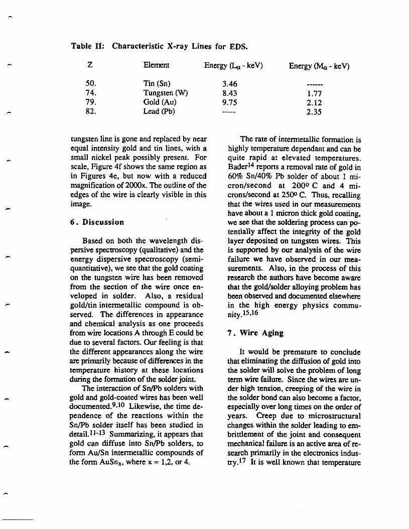
The electron range at 15 ke V in gold is estimated to be about 0.53 microns, with the x-ray generation volume less than this range because below a certain energy the electron does not have suffi • cient energy to excite the characteristic x • ray line.8 The elements of interest in our study and their atomic numbers are: tin (50), tungsten (74), gold (79), and lead (82). These elements along with their characteristic x-ray emission lines of interest are shown in Table II. The characteristic x-rays are labeled La or Ma. depending on whether an L or M orbital electron was ejected from the atom by the microprobe electron beam.
Figure 4a shows a strong gold La line, with no other significant peaks in the spectrum. Figure 4b corresponds to a point on the wire that was just inside the solder joint. Again, a strong gold line is seen with a very weak tin line. As we move deeper into region where the wire was soldered, an area is encountered, shown in Figure 4c, where a tungsten x-ray line appears, indicating a thinner/absent gold layer, and approximately equal intensity gold and tin lines. Note that comparing relative intensities between lines does not necessarily correspond to relative concentrations of these elements. Additionally, a small amount of nickel may be present although the line is not too definitive.
Proceeding to the higher magnification images of location D (Figure 4d), a specific area located between the mottled surface structure shows a strong tungsten line, without any other significant lines present Moving the electron microprobe slightly upward onto one of the surface prominences (Figure 4e), shows that the
-
---
-...
..
..
...
•
-
-
Table II: Characteristic X-ray Lines for EDS.
z Element Energy (Lu - keV) Energy <Ma - keV)
50. 74. 79. 82.
Tin (Sn) Tungsten (W) Gold (Au) Lead (Pb)
tungsten line is gone and replaced by near equal intensity gold and tin Jines, with a small nickel peak possibly present. For scale, Figure 4f shows the same region as in Figures 4e, but now with a reduced magnification of 2000x. The outline of the edges of the wire is clearly visible in this image.
6. Discussion
Based on both the wavelength dispersive spectroscopy (qualitative) and the energy dispersive spectroscopy (semiquantitative), we see that the gold coating on the tungsten wire has been removed from the section of the wire once enveloped in solder. Also, a residual gold/tin intermetallic compound is observed. The differences in appearance and chemical analysis as one proceeds from wire locations A through E could be due to several factors. Our feeling is that the different appearances along the wire are primarily because of differences in the temperature history at these locations during the formation of the solder joint.
The interaction of Sn/Pb solders with gold and gold-coated wires has been well documented.9,10 Likewise, the time dependence of the reactions within the Sn/Pb solder itself has been studied in detail.11-13 Summarizing, it appears that gold can diffuse into Sn/Pb solders, to form Au/Sn intermetallic compounds of the form AuSnx. where x = 1,2, or 4.
3.46 8.43 9.75
1.77 2.12 2.35
The rate of intermetallic formation is highly temperature dependant and can be quite rapid at elevated temperatures. Bader14 reports a removal rate of gold in 60% Sn/40% Pb solder of about 1 micron/second at 2000 C and 4 microns/second at 2500 C. Thus, recalling that the wires used in our measurements have about a 1 micron thick gold coating, we see that the soldering process can potentially affect the integrity of the gold layer deposited on tungsten wires. This is supported by our analysis of the wire failure we have observed in our measurements. Also, in the process of this research the authors have become aware that the gold/solder alloying problem has been observed and documented elsewhere in the high energy physics community.15,16
7 • Wire Aging
It would be premature to conclude that eliminating the diffusion of gold into the solder will solve the problem of long term wire failure. Since the wires are under high tension, creeping of the wire in the solder bond can also become a factor, especially over long times on the order of years. Creep due to microstructural changes within the solder leading to embrittlement of the joint and consequent mechanical failure is an active area of research primarily in the electronics industry .17 It is well known that temperature
cycling can accelerate creep in solder bonds. IS However, it is very difficult to simulate the effects of Jong term creep by standard accelerated aging tests.
The L3 experience can be invaluable in assessing the effects due to creep in solder bonds under mechanical loading over years of operation. We recommend that continued testing should be conducted to analyze actual failed wires from the L3 experiment when it is possible to rettieve them.
8. Conclusions
We have observed and analyzed a 25 micron diameter gold-plated tungsten wire that has pulled out of a tin/lead solder bond under uniform tensile loading. The wire attachment process was similar to that used in current high energy physics muon drift chamber sub-systems and proposed for future drift chamber systems. Visual observations were carried out using optical and scanning electron microscopy, while chemical analysis was carried out in a microprobe using both wavelength dispersive and energy dispersive spectroscopy. The results of the analysis indicate that the gold coating on the tungsten wire reacts with the tin/lead solder to form a gold/tin intermetallic compound. We would surmise that a surrounding lead-rich region exists, leading to a weakening of the wire/solder interface.
In the case of the specific guard wires in L3 muon drift chambers, wire failure can, and has been observed to, occur. However, since we have observed this failure mode only once in our own studies, we suspect that the ultimate failure mechanism may be time-dependent. We are currently weighing the benefits of aging tests that would accelerate the phenomena, yet not introduce artifacts.
However, the most applicable data to apply to future wire chamber designs can be found in the current generation of experiments utilizing large wire chamber systems such as L3.
Acknowledgements
The authors gratefully acknowledge the technical assistance of Linda Durbin for mechanical testing and Don McCoy and Jim Yoshiyama for microprobe analysis and Ileana Dobie for the handling of administrative matters.
This work performed under the auspices of the U.S. Department of Energy by the Lawrence Livermore National Laboratory under Contract W-7405-ENG-48.
References
1. B. Adera, et al., "The Construction of L3", Nucl. Instr. Meth. A289, p. 35, 1990.
2. The L"' Collaboration, "Expression of Interest to the SSC Laboratory", May 1990.
3. M. Matoba, T. Mirose, T. Sakae, H. Kametan, H. Ijiri, T. Shintake, 'Three Dimensional Monte Carlo Simulation of the Electron Avalanche Around an Anode Wire of a Proportional Counters," IEEE Trans. Nucl. Sci., NS-32, #1, p. 541, 1985.
4. M. White of the L3 collaboration, private communication.
5. John A. Kadyk, "Wire Chamber Aging", Nucl. Instr. Meth., A300, p.436, 1991.
-
-
-
-
----..
...
-
-
-
6. D. B. Masson, B. K. Kirkpatrick, "Equilibrium Solidification of SnAg-Sb Thermal Fatigue-Resistant Solder Alloys," J. Electronic Materials, 15, p. 349, 1986.
7. J. I. Goldstein, D. E. Newbury, T. Echlin, D. C. Joy, C. Fiori, E. Lifshin, Scanning Electron Microscopy and X-Ray Microanalysis, Plenum Press, p. 92 (1981 ).
8. ibid. p 72. We use the KanayaOkayama range estimate.
9. R. Keeler, "Specialty Solders Outshine Tin/Lead in Problem Areas," Electronic Packaging and Production, p. 45, July, 1987.
10. D. R. Frear, W. B. Jones, K. R. Kinsman, eds., "Solder Mechanics: A State of the Art Assessment," TMS EMPMD Monograph Series, p. 58 (1990).
11. B. T. Lampe, "Room Temperature Aging Properties of Some Solder Alloys," Welding Research Supplement, p. 330s, October, 1976.
12. P. G. Harris, K. S. Chagger, M.A. Whitmore, "The Effect of Aging on the Microstructure of 60:40 Tin-lead Solders," Soldering & Surface Mount Technology, No. 7, p. 20, February, 1991.
13. D. Tribula, D. Grivas, J. W. Morris, Jr., "Stress Relaxation in 60Sn-40Pb Solder Joints," J. Electronic Materials, 17, p. 387, (1988).
14. W. G. Bader, "Dissolution of Au, Ag, Pd, Cu and Ni in a Molten TinLead Solder", Welding Research Supplement, p. 55s, 1969.
15. P. Schilly, et al., "Construction and Performance of Large Multiwire Proportional Chambers," N ucl. Instr. Meth., 91, p. 221, 1971.
16. D. Schmidt, "Technology of Drift Chambers," Nucl. Instr. Meth., 176, p. 39, 1980.
17. J. H. Lau, D. W. Rice, "Solder Joint Fatigue in Surface Mount Technology: State of the Art," Solid State Technology, p. 91, October, 1985.
18. D. Tribula, D. Grivas, D.R. Frear, J. W. Morris, Jr., "Microstructural Observations of Thermomechanically Deformed Solder Joints", Welding Research Supplement, p. 40s, October, 1989.

2s 11m
Anode wire
Figure 1. Schematic representation of a simulated electron avalanche near a sense wire in a multiwire proportional chamber. (from Ref. 3)
-..
-
-...
...
...
...
..

A B I I
C D I I
E I
Secondary Electron Imaging (SEI) 200x
(a)
Backscattered Electron Imaging (BEi) 200•
(b)
Figure 2. The image on the left (Fig. 2a) is a secondary electron image (SEI) of the failed wire end. SEI is more sensitive to the surface structure. The locations A through E correspond to specific regions of the wire that were looked at in greater detail in the study. The image on the right (Fig. 2b) is a back-scattered electron image (BEi) the the same wire. This image is more sensitive to atomic number with brighter areas corresponding to higher atomic number. Both images are magnified 200x.

Figure 3. Secondary electron images (SEI) of the failed wire at locations A through E (Figs. 3a-e, respectively). The images progress from the unsoldered portion of the wire at location A, showing the relatively smooth surface of the gold-coated tungsten wire, to the tip of the wire at location E, showing a mottled surface consisting of "beaded up" metal.
-
--
-
--
-
-

(a)
(b)
(C)
Backscattered Electron Imaging (BEi) 2000x
Area "B" ·soldered, allpped portion of Au-coated W wire.
Backscattered Electron Imaging (BEi) 2000x
Area .. C" • transHlon ponlOn 01 Au-coated W wire near sllp
EDS Spectrum Of Area ·c-
Figures 4a-c. Back-scattered electron images (BEi) of 1he failed wire with accompanying chemical analyses as given by energy dispersive spectroscopy (EDS). Cross-hairs indicate the location of the electron beam microprobe, which is actually sma1ler lhan the dimensions of the cross-hairs. The chemical anaJyses for each image show intensities and of characteristic x.-rays and computer idcntifica1ion of the clements associated with the x-rays. The wire locations A - Care examined in these images at a magnification of2000x.

(d)
l•J
(I)
Area "D". soldered, sllpped portion of Al;C:Oattct w wtre. . ~~~m•-·-· ~;;.i· ·: "' -~~~~ ~~~ •:tr~ Backat:a-~llnlglf11 /BEi/
sooox Area "D"' • solMred, slipped PQnlOn ol Au-coatftd w wire.
~~~"----~
Backseanered Electron ltnaglng (BEi} • sooox
Aru '"E". SOidered. allpped Portion Of Au-coatw w wire.
Figures 4d-f. Back-scattered electron images (BEI) of the failed \Yire with accompanying chemical analyses as given by energy dispersive spectroscopy (EDS). Location Dis magnified 5000x in figs. 4d and 4e. 1'he electron beam microprobc is located at slightly different areas on the surface of the Wire, as indicated by the cross-hairs. In Figure 4d, the microprobe is cc»zt:,ret} .on a J
1.:ille)' betweea the lx:a.ded up nu:ta.l a.nd the chemical analysis indicates tungsten only. In Figure 4e, the microprobe is centered on an area of beaded metal and the chemical analysis indicates the presence of gold, tin and nickel, with no tungsten. Figure 4f is an image of the same location as Fig. 4e but at a reduced magnificalion.
APPENDIXC
UCRL-JC-105646
ELECI'RO-OPTIC TRANSIENT IMAGING INSTRUMENTATION DEVELOPMENT ATLAWRENCELIVERMORENATIONALLABORATORY:
IMPLICATIONS FOR SSC INSTRUMENTATION DEVELOPMENT

Electro-Optic Transient Imaging Instrumentation Development at Lawrence Livermore National Laboratory:
Implications for SSC Instrumentation Development*
Marl< Lowry, Barry Jacoby, and Hal Schulte Lawrence livermbre National Labormory
Livermbre, California 94550
Introduction
Over the last decade, the underground weapons physics laboratories fielded by LLNL's Nuclear Test and Experimental Sciences (NTES) program have experienced marked change. This change is characterized by a phenomenal growth in the amount of data returned per event These techniques have been developed as a result of the severe demands placed upon transient instrumentation by the physics requirements of our underground nuclear laboratories. The detector front-ends must quickly detect, process and transmit a large volume of data to recording stations located approximately 1 km from the event. In a recent event, the delector front-ends successfully handled data at a prompt rate of approximately 13 Terabitslsec. Largely, this advance can be auributed directly to the increased use of electro-optic techniques.
These highly-parallel high-bandwidth imaging instrumentation systems developed for the test program may have a lot to offer the high-energy physics community tackling the challenge of the unprecedented luminosity and fidelity demands at the SSC. In what follows, we discuss details of a few of our prompt instrumentation techniques and compare these capabilities to the detector requirements for the challenging physics at the SSC.
Underground Weapons Physics Instrumentation
The power of these instrumentation developments is perhaps best illustrated by the x-ray imaging/spectroscopy experiment illustrated in Figure I. Here the x-ray output from a nuclear event is spectroscopically dispersed by the bent-crystal spectrometer onto a fast fluor material (CdS, WL1201, etc.). The fluorescence is then coupled via coherent fiber arrays to streak cameras approximately 10 meters away. The streak camera is then read out by a very high-speed CCD camera.1 Spatial sampling of the x-ray output through this system then yields an image of the event that is time resolved, specttally resolved, and spatially resolved. In effect, a specttally resolved x-ray motion picture of the event results.
To gain an appreciation for the information content of such techniques, let us first reflect on the number of independent data channels such a system yields. The limit on the number of spatial pixels is usually determined by the number of CCD pixel elements in the spatial direction on the streak camera (typically 380), the spatial resolution of system, and sampling considerations; the resulting number of independent channels is typically 100. The number of resolvable time samples for each of these channels is another dimension to the total data content. Here the time resolution is limited by several system considerations: the number of CCD pixels in the time direction (usually 122), often times the fluor lifetime, dispersion in the optical fiber, and sampling considerations. This time resolution is typically 1 ns, and the experiments are usually configured such that there would be 122 time samples, for a record length of 30 ns. The final dimension of the total data return is then the dynamic range (number of readable bits), and our current systems are capable of a dynamic range of 8 bits (presently going to 10 bits), with a precision of approximately 1 %. Finally, we may calculate the prompt data rate as (N n b t)!I'. Where N is the number of streak camera systems used, n is the number of channels per camera used, b is the dynamic range of each in bits, t is the number of resolvable time bins, and T is the temporal record length. In a recent event, where sixteen streak cameras were fielded, this piece of arithmetic yields the astonishing value of approximately 13 Terabits/sec for the prompt data capture rate.2
As powerful as these fluor-based imaging techniques are, we have found severe ttade-offs between sensitivity and bandwidth that renders these techniques unsuitable for some applications that require good temporal response and high dynamic range. Not only does increased fluor speed usually result in less efficiency--through poisoning or shon-circuiting of the fluorescent ttansitions with faster non-radiative channels, the optical output of the fluor is not well-matched to the propagation characteristics of optical fiber. The output of fluors is almost always isottopic and the spectrum is quite broad. These charac·
• This work was performed under the auspices of the U.S. Dcpanment of Energy by the Lawrence Livermore National Laboratory under contract number W-7405-ENG-48.

Re<0rding TnilerSGZ
•
Fil>er tics
Tngger Detectors , • Source
X·nys neu-.s gammas
Beam
•lop ·1'.•1 ,,,~
-~~, .. , , .. ., 1 ,,,,_, ,. I
-of"""~"·'' -:;~·· ·~ , _, ,,, - ,.,,, .. ,. eters,, ,1"
I 1 I• - ,1,11 _, ~t•' -:-_,
Active Detector
I lOOOm F.0.
Figure 1. An example of LLNL's transient imaging insaumentation--time-resolved remote spectroscopy.
teristics lead to modal and chromatic dispersion, respectively, and can severely limit the bandwidth of such systems. Modal dispersion in 200 micron core fiber for instance is approximately 80 picoseconds/meter. The only cure is to limit lhe extent of the specuum used (or use complicated spectral equalization teehniques>3 and limit the numerical apenure of the system; both measures lead to decreased sensitivity. Thus, for system temporal responses better than I ns with good sensitivity, other approaches are sought.
To better taylor the optical source to optical fiber, lasers are the obvious source of choice. However, encoding an electrical signal directly onto the gain mechanism of a laser is very difficult to do well at high frequency: the lasing mechanism is fundamentally very nonlinear in a dynamic sense,4 therefore, the modulation is often chaotic at frequencies near or beyond the relaxation oscillation frequency. Since 1985, we have been pursuing development
2
of integrated optical modulators to fill the role of encoding electrical signals onto an optical carrier in a very high bandwidth instrumentation system. By separating the functions of light generation and signal encoding. it is much easier to produce a more useful optical carrier while also allowing great flexibility in the characteristics of the signal encoding, i.e. the mapping of voltage or charge to optical power/energy space. For many electronic systems, linearity, not flexibility, of system response is the goal. However, nonlinearities as long as they are well behaved (not dynamic) can be successfully incorporated into instrumentation systems as we show below, and can be a tremendous sensitivity "lever" as discussed in the following paper.'
As we have hinted, there arc many types of modulator schemes. A fundamentally important design is illustrated in Figure 2. The Mach-Zehnder modulator operates as follows. The optical carrier is injected into the single-mode waveguide on the lithium niobatc substrate
...
-...
...
-...
-
-
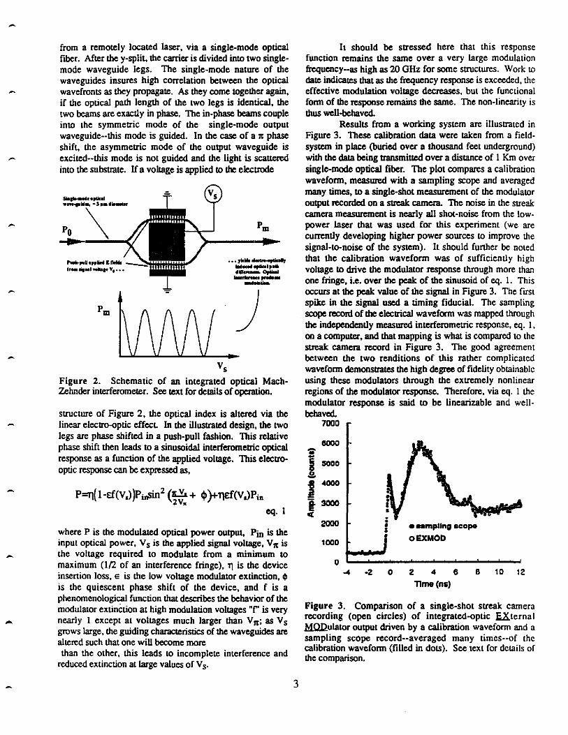
-from a remotely localed laser, via a single-mode optical fiber. Afcer they-split, the carrier is divided into two singlemode waveguide legs. The single-mode nature of the waveguides insures high correlation between the optical wavefronts as they propagate. As they come together again, if the optical path length of the two legs is identical, the two beams are exactly in phase. The in-phase beams couple into the symmetric mode of the single-mode output waveguide--this mode is guided. In the case of a 1t phase shift, the asymmetric mode of the output waveguide is excited--this mode is not guided and the light is scatiered into the substrate. If a voltage is applied to the electrode
..... ,..u 1ppW E new. --.;: ,,_._ .. ,....,,,v, ...
Vs
... ,.. ........ .,. .. ., ........... , .... ••-o,tkal ---·-)
Figure 2. Schematic of an integrated optical MachZehnder inierferomeier. See cext for details of operation.
structure of Figure 2, the optical index is altered via the linear electro-optic effect In the illustrated design, the two legs are phase shifted in a push-pull fashion. This relative phase shift then leads to a sinusoidal interferometric optical response as a function of the applied voltage. This electrooptic response can be expressed as,
P=ri( 1-Ef(V,) )P;,.9n2 (l!..Y.. + cj> )+11ef(V,)P;n 2v.
eq. 1
where P is the modulated optical power output, Pin is the input optical power, Vs is the applied signal voltage, V1t is the voltage required to modulate from a minimum to maximum (112 of an interference fringe), Tl is the device insenion loss, e is the low voltage modulator extinction, Cl>
is the quiescent phase shift of the device, and f is a phenomenological function that describes the behavior of the modulator extinction at high modulation voltages "r' is very nearly I except at voltages much larger than V1t; as Vs grows large, the guiding characteristics of the waveguides are alcered such that one will become more than the other, this leads to incomplece interference and
reduced extinction at Large values of Vs·
3
It should be stressed here that this response function remains the same over a very large modulation frequency--as high as 20 GHz for some structures. Work to dace indicaces that as the frequency response is exceeded, the effective modulation voltage decreases, but the functional fonn of the response remains the same. The non-linearity is thus well-behaved.
Results from a working syscem are illustrated in Figure 3. These calibration data were taken from a fieldsyscem in place (buried over a thousand feet underground) with the data being transmitted over a distance of I Km over single-mode optical fiber. The plot compares a calibration wavefonn, measured with a sampling scope and averaged many times, to a single-shot measurement of the modulator output recorded on a streak camera. The noise in the streak camera measurement is nearly all shot-noise from the lowpower Laser that was used for this experiment (we are currently developing higher power sources to improve the signal-to-noise of the system). It should funher be noted that the calibration waveforrn was of sufficiently high voltage to drive the modulator response through more than one fringe, i.e. over the peak of the sinusoid of eq. I. This occurs at the peak value of the signal in Figure 3. The first spike in the signal used a timing fiducial. The sampling scope reconl of the electrical waveform was mapped through the independently measured incerferometric response, eq. I, on a computer, and that mapping is what is compared to the streak camera record in Figure 3. The good agreement between the two renditions of this rather complicated wavefonn demonstraces the high degree of fidelity obtainable using these modulators through the extremely nonlinear regions of the modulator response. Therefore. via eq. I the modulator response is said to be linearizable and wellbehaved.
7000
aooo -;;--i 5000
.!!.
J - •
i 3000 • I C( •
2000 : • • .. mpllng acope '
1000 oEXMOD
0 -4 -2 0 z 4 6 8 10 12
Time (ns)
Figure 3. Comparison of a single-shot streak camera recording (open circles) of integrated-optic .EXternal ~ulator output driven by a calibration wavefonn and a sampling scope record--averaged many times--of the calibration wavefonn (filled in dots). See text for details of the comparison.

Conclusions
The instrumentation systems discussed here are in many ways capable of exceeding the requiremenis of the SSC, especially in terms of temporal response, data-density and remote recording; adaptations of these techniques may prove to be exceedingly well matched 10 SSC detector rcquiremenlS.
We see sim ilarilies between the changes experienced by our own NTES program over the last decade, and the changes in teehnology that appear necessary to meet the challenge or high-energy physics (HEP) instrumentation for the SSC and into the neit century. While the optimum solution to HEP instrumentation will not be identically what we have reviewed here, it does appear inevitable that the techniques will move in this direction.
Acknowledgements
Thanks are due to Richard Bionta and Mark Eckart of LLNL for recognizing the potential applicability of LLNL/NTES instrumentation techniques to the SSC. We also thank Dick Lear and Dick Fortner of LLNL for their support and encouragement Several individuals who participated in the first fielding of LLNL integrated optical modulators for the HORNITOS event are recognized for their achievemenis and contributions IO the instrumentation development Greg Lancaster {LLNL), Dan Nelson (LLNL), and Phil Watts (EG&G).
References
I M. E. Lowry and B. A. Jacoby, Ulrra High-Speed Single-Slwt Electronic Imaging, invited paper in the Proceeding of the Applications of Electronic Imaging Conference, January 1989, Los Angeles, SPIE Vol. 1082.
2 II should be noted that the single-transient nature of the event allows us IO stretch out the transmission time of the bit stream without the pile-up difficulties associated with collider instrumentation. Nonetheless, as we show in the following paper, with appropriate triggering similar techniques may be applied to SSC instrumentation.
3 R. P. Reedy, F. Roeske, Jr., and D. E. Smith, FiberOptic Spectral-Streak Equalizer, Rev. Sci. Instr. Vol. 56, 7. pp. 1356-1367.
4 See for instance pp. 954.975 in A. E. Siegman, Lasers, University Science Books. Mill Valley, California (1986).
5 M. E. Lowry, E. Ables, R. M. Bionta, R. E. Haigh, K. F. Hugenberg. R. Kalibjian, C. F. Mcconaghy, D. Milton. M. D. Roller, and H. F. Schulte, An ElectroOptical Imaging Approach to the Prompt Signal Processing Problem of Mega-Channel SSC Detector Arrays. the following paper in these proceedings.
4
...
...
-
...
•
...
...
...
...
-
...

APPENDIXD
UCRL-105645
AN ELECTRO-OPTICAL IMAGING APPROAOI 101HE PROMPT SIGNAL PROCESSING PROBLEM OF MEGA-OIANNEL SSC DETEClOR ARRAYS
An Electro-Optical Imaging Approach to the Prompt Signal Processing Problem of Mega-Channel SSC Detector Arrays
Mark U>wry, Eldon Ables, Richard Bionta, Ron Haigh, Keith Hugenberg, Ralph Kalibjian, Charles McConaghy, Darin Milmn, Mark Rotter, and Hal Schulte
Lawrence Livermore Nmional Laboratory Livermore, California 94550
Introduction
The physics demands of high luminosity at I.be SSC and I.be sometimes subUe measurements required to elucidate new physics will undoubtedly tax existing instrumentation. As is I.be case with most experimental fields, new physics follows from better measurement concepts and technologies. We expect I.bis to be I.be case with the SSC as well. In what follows, we offer a glimpse of what may be possible using some of I.be recent results from the emerging technologies in the field of electro-optics.
A Proposed Electro-Optic System Architecture
The large number of channels required for SSC instrumentation and the temporal resolution required lead quite nalurally to the consideration of elecrro-optical imaging
- - - - -- - - -- -- -.
techniques. I This is particularly true with the need lO establish reliable and prompl event triggers tha1 are based upon mtal energy and even! topology, as we shall see with I.be system ouUined in Figure !.
Here we start with more-or-less conventional HEP detectors that yield charge as the measurement output. This charge is then used to modulate an externally provided optical carrier signal {amplifiers and pulse shaping may not even be required, as will be seen in what follows). The basic ideas regarding the optical modulalOr are discussed in ref. l . The optical carrier may be supplied by some, hopefully small, number of fibers that provide optical power lO a chip containing many of the modulators discussed in ref. I. The optical power division is accomplished on a chip as well (perhaps monolithically integrated with the modulator chip). This large
p, .......
••• lntegr.a.d I BHm Giiied
Qpllcol CCD Computer Controll•r ·-· : 0.IK:;:lo:;_• --1>-j
I
• 1D' :
ch•nn•ls
Modulator• F ... r apfftter CCD
n'r.a= ..... ~§!§1 ~_,'::'"9.., ..... ,...' ... "" ... ~ ... !'".,.1oy_' ___ eo~m•ra
.. _________ _ Dfacrtndnator
Progr•mMH -IH-- SpMilll Fitter Fourier filler Fron1~enc1 Proceaelng
Loc819d on Oet9etor Photo diode 1- _____ .,, DlscrimlMtOr
Loc.ted in Delector
I I
...._ _ - - I
~ ..... Level 1 trigger energy MUns on photo diode
___ ~ Remotely Locattd Anl-tlme
Oplical•trtgger Formation
Level 2 Trtaa•r Founer.CUt•red energy-ffMI lopolog)' discriminalion
Figure I. Proposed elcctto-optic system architecture for high luminosity data acquisition at the SSC. Some key features arc the use of ultra-sensitive integrated-optical modulators and the use of optical pattern recognition for trigger formation.
• This work was performed under the auspices of the U.S. Department of Energy by the Lawrence Livermore National Laboratory under contract number W-7405-ENG-48.

number of independent optical channels (perhaps as many as 100 arc possible per chip) are brought off chip in individual optical fibers. These optical fibers arc arranged in an imaging bundle-such that image information is preserved. In the event of a hit, this bundle is then the conduit of a transient image that propagates to the level-one trigger.
The first step in the trigger generation process is to pick-off a portion of the image power through use of a conventional optical beam splitter. Let us call these beams, after the splitter, the trigger image and the major portion the record image. The trigger image can be split into two beams. In the case of data from a calorimeter, one leg of the trigger beam can be spatially filtered with a filter whose optical density is graded as, sin(9), where 9 is the angle with respect to the beam direction for that pixel element. As this filtered image is relayed optically to a large area photodetector, the output charge from the photodiode is then a prompt meas me of the total transverse energy-the delay for this part of the trigger formation is just the response time of the photodetector; a few nanoseconds is easy.
The second portion of the trigger image can be used to perform relatively complex event topology discrimination through the use of well-established optical pattern recognition techniques. The most straight-forward technique applies again to the case of calorimetry. By applying the optical Fourier transform to the second trigger ima~~ealized conveniently with the use of simple optical lenses -one can perform spatial frequency filtering operations by simply placing the appropriately patterned spatial transmission filter in the Fourier plane (by using the new technologies of spatial light modulation,3 the characteristics of this frequency filter could be conveniently controlled electronically). The output of the spatial filter is then relayed to another large area photodetector. The prompt optical sum performed by this photodetector is a measme of the energy content only of features of the event that have a frequency content that is matched to the spatial filter in the Fourier plane. This then allows us to discriminate promptly (a few nanoseconds) on the basis of event topology, as well as total event energy. It should be noted that optical processing has at least one precedent4 in HEP instrumentation.
Perhaps this optical pattern recognition may be extended to the case of tracking detectors. It may be possible to use the optical Hough transformation to detect the existence of stiff tracks. The Hough transformation maps straight lines into points-one coordinate of the point being the line's angle with respect to the abscissa, and the other is its distance from the origin. Using techniques similar to the optical Fourier transformation, the Hough transformation may be accomplished optically.5, 6 It may prove possible to optically correlate this trigger with the calorimeter information to provide an elegant and comprehensive· trigger, promptly, and with little or no electronics in difficult environs. It must be pointed out that all the optical Hough transformation work that we have seen to date is accomplished with a mechanically rotating optical clement, and thus would be far too slow for HEP instrumentation. However, there may be a way to realize the transform
2
in optical fashion instantly, and we are currently exploring that possibility.
We have thus far painted a simple picture of Fourier optics techniques. Our laboratory measurements to date-and some reflection on the Fourier optics theory-would suggest that performing the Fourier transform of the image from an optical fiber bundle may be very difficult Basic Fourier optics work is done with the use of simple apenures, and the optical wavefronts employed are coherent. In our case, the individual image pixels have probably suffered large relative optical phase shifts. These phase shifts lead to severe interference noise in the Fourier plane. We can suggest three possible ways around this relative phase shift problem.
First. the fact that our opticalcarrier was derived from a single laser (or perhaps a phase locked set of lasers) may allow us to adjust these relative phases such that when we arrive at the Fourier plane the relative phase shifts have been compensated. Further, the use of integrated optical devices as our signal encoding mechanism may provide a convenient solution. The most fundamental form of optical modulation is the phase shifter. In fact. the Mach-Zehnder modulator discussed in ref. I iscomposedoftwosuchdevices. Aphascshiftercould be employed in each channel to compensate these phase shifts in response to the input from a feedback mechanism. Another phase compensation technique would be the use of a holographic element in the image plane after the bundle, this element could be used to compensate the optical phases of the individual image pixels by focusing the image onto this holographic phase plate.7 We are exploring both of these phase compensation techniques, and hope to carry-out experiments soon. Finally, the partially coherent image from the fiber bundle could be transformed into an incoherent image. This may be achieved by imaging the fiber output unto an image intensifier. The image intensifier output is then incoherent light from the phosphor screen. Then the incoherent image could be processed using incoherent processing techniques. This offers the added advantage of allowing the image information to be gated; however, to retain the speed of the optical processing fast phosphors must be used-so, the gain of the intensifier may then become an issue.
The remaining beam, the record image, can be refocused onto another imaging optical fiber bundle, and be allowed to propagate for however long is required for com plcte trigger formation. After trigger formation, the image is captured by a gated ultra-fast readout CCD imager. Image readout times of IO µs for IO,OOOpixels with a dynamic ranges of 1,000 are attainable with today's technology. Extended dynamic ranges could be attained by using a slightly higher power optical carrier and splitting the record image with a I 0:90 beam splitter and recording both images.
The advantages of using this electro-optical imaging approach arc several:
The transmission media (small diameter optical fibers with approximately lcm2 cross-sectional area per I 0,000 fibers) offers low radiation scattering, and a mechanically manageable cable plan.
...
...
-""
""
...
...
--...
...

HP 8111 A Signal Generator Trig.Out I MHz Sine Wave
•4 V P-P Out
Modulating I Signal Mach-Zehnder
v.,.. •4V D.C. Bias Supply
.,,. Var.
Out
/""' Auen. Trig.
0
AG
AMOC 1300nm C.W.Y
,, 7854Scope
Bias-T
I Mach-Zehnder - - PD. ~ - - v D
PD. - Photodiode - - Optical Signal
ORTEC 450 Amp. 0.1 us Differentiation Time
Constant
Figure 2. Experimental layout for Mach-Zehnder dynamic range measurements.
Since all channels are brought outside in parallel, triggering architectures become very flexible and amenable to modification in lhe future.
• Ground-loopsandolherformsofEMibecomelessof a problem.
• The modulators and fiber medium easily support lhe required temporal response.
• The power consumption can be much less lhan 1 mW per channel for lhe power-dissipation critical innertracker applications. The fiber medium conveniently provides signal delay to accommodate lhe trigger formation time.
• The potential for operation wilhout amplifiers (discussed in detail below) adds greatly to system reliability-particularly for lhe high radiation environments. Optical pattern recognition and optical summing techniques can be applied for prompt trigger formation.
While this total system architecture is quite attractive in many respects, we should not overlook lhe value of any one of lhe roughly lhree major subsystems: lhe optical modulators, the image processing techniques, and lhe fast CCD data capture. We will spend lhe rest of the paper addressing the optical modulators.
3
Integrated Optical Modulator Results
While we have been pursuing instrumentation development wilh modulators for several years, we have only recently considered lhem in lhe context of HEP experiments. To that end, we set out to understand how they might best be used in HEP experiments. A potential application of the technology is in calorimetry experiments, where exceptional dynamic range is required. We have made measurements of dynamic range at 800 nm, using 2x2 modulators, and measurements at 1300nm using Mach-Zehnder modulators. Due to the limited space, we will only discuss the Mach-Zehnder measurements here.
The experimental seblp is outlined in Figure 2. We used a sine-wave electrical input for convenience. but the conclusions should apply to pulse operation as well. The bandwidth of the system was limited by the amplifier at 1.5 MHz. The bias applied to lhe modulator was adjusted by observing the signal-to-noise of a very weak signal; at the point of maximum signal-to-noise, the bias voltage level was fixed. Figure 3 shows the result of three different levels of electrical auenuation (on the sinusoidal input signal) ranging from 0 dB to80dB (voltage). Even with 80dB auenuation (x!0,000), the output signal from lhe modulator is easily seen on the scope trace. For the 0 dB trace, the negative going portion of the sinusoidal input is distoned as it passes through the minimum
in the sinusoidal response function (see ref. I), however the positive going portion does not go through the response peak (indicating that the modulator was not biased precisely at the half-power point). Concentrating on the positive going portion of the sinusoid, we see that the input signal goes through a dynamic range of at least 10,000. At the lowest input signal level (80 dB attenuation), the signal is still much above the noise. By analyzing therms noise of our system with the light beam blocked, and with the beam unblocked but no modulation signal, we find that at the attenuation value of 10,000 the ratio of the peak signal IO the noise due IO just the laser/ modulator combination is - 4. However, these noise measurements were made from seope traces of the same time scale as Figure 3; here the noise bandwidth is determined by the amplifier roll-off at I. 5 MHz, and the record length at the low end; we find this IO be 1.3 MHz. Extrapolating IO the case of a I 0 MHz bandwidth (more suitable for most SSC applications), we find that this increase in bandwidth should lead IO a noise increase of a facior of c 2. 77. Thus operating with a bandwidth of IO MHz, we would expect IO find a dynamic range of • ( 4/ 2.77)(10,000) or slightly more than 14,000. Further. since we know that this signal can be linearized, we can establish a linear relationship between the optical power from the modulalOr and the input voltage IO the modulaior.
At this point, it is convenient to discuss the relationship of the charge (or voltage sensitivity) to the parameters of the carrier modulator system. The optical power output of most modulators can be conveniently described by
P=PoF(V) eq. I
where Po = 11Pin is the maximum carrier power out of the modulator-when F(V)= I, 11 is the insertion loss. Pin is the input optical power, and F(V) is some modulation function of charge or voltage. The uncertainty of the measured optical throughput, ilP, is made up of three contributions: carrier power instabilities, deteclOr noise, and amplifier noise. We may lump these uncertainties togetherinlO the iota! uncertainty in the measured power, ilP. The voltage uncertainty due 10
fluctuations in the measured optical power is given by
llV=(llP/Po)/(dF /dV) eq.2
assuming that ilP is small compared IO Po, and dF/dV is not close IO zero. Any fluctuations from the modulator itselr8 are then added in quadrature with this uncertainty IO arrive at the total uncertainty in the measured voltage.
For the case of the Mach-Zehnder, reproducing eq. I from ref. I we note that
P=tl( 1-Ef(V,))P;,,sin2 (~+<I> )+11Ef(V,)P;n zv. eq. 3
whereP is the modulated optical power output, Pin is the input optical power, Vs is the applied signal voltage, V" is the voltage required IO modulate from a minimum IO maximum (I ( 2 of an interference fringe), 11 is the device insenion loss.£ is the low voltage modulalOr extinction and usually e < 0.0 I, <I> is
Output Signals - 1300 nm Mach-Zehnder Greater than 80 dB (Voltage) Dynamic Range
-::s c.. :;
15 ..--,--,~~--.,--.,...--,...~--,---,--.,.___~~,--,,--~~--.,----,----,-~~. . i
(\ r~
! j ' . l ;., \ f'\\ ' " ;;
~= ,
\\ :) ~; !j
05 " ~:
, i \ i
"' ' ' jf ~~
·!
' ., -··1
0 -05 \ \/ / j '"i
'
-1 0 2 3
time (µs)
... : .. ' ... , : '• w
4
\~~-.. ! ·i i -;
5
Figure 3. Results of Mach-Zehnder dynamic range measurements. A dynamic range well in excess of 10,000 is demonstrated.
4
--
-
...
-
--
-...

the quiescent phase shift of the device, and f is a phenomenological function that describes the behavior of the modulator extinction at high modulation voltages "r' is very nearly I except at voltages much larger than v7t9· With dF/dV at its maximum (i.e., at the half-power point, in the Mach-Zehnder case), we find,
oQ =file.: (oP/l'o~ Q, V • 7t(l ·E) eq.4
so the voltage (charge) uncertainty is proportional to the relative optical power uncertainty, scaled by V lt(Qi).
For the measurements shown in Figure 3 extrapolai:g to 10 MHz, 'Ov/vx= !/(dynamic range)= 1/14,000 = 7.lxlO Equivalently, 'OQ/Oit = 7.lxl0-5 Alternatively one may extract the relative optical power uncenainty using eq. 4, art Po=l.1=10-4. The modulator used for the measurements in Figure 3 was an in-house designed and fabncated h1ghbandwidth traveling wave Mach-Zehnder. In general, for SSC applications it appears that lumped elementelecuodestructures may be preferred; to understand the charge sensitivity possible for SSC applications let's consider the lumped element case. BeckerlO discusses a figure-of-merit for lumped-element modulators: M= V lt L, where L is the length of the elecuode structure. Becker finds that M= 14 V-mm and that the capacitance/elecuode length p =0.85 pF/mm . Thus, one can easily calculate the amount of charge deposited on the electrode structure to yield a voltageofV"; Qx=Mp=l2 pC. Applying this to our dynamic range measurements above yields the result that the minimum charge that we are capable of detecting would be 12 pC/14,000 = 0.86 femtocoulombs. This assumes our value of the relative optical power uncertainty extrapolated to 10 MHz bandwidth, and the Oit of a lumped element modulator structure. We are further making the tacit assumption that the electrode tennination resistance is large enough (or actively gated) so that the charge will not dissipate on time scales consistent with the desired bandwidth.
It is useful to consider the shot noise (counting statistics) limitations on the dynamic range. For our optical power level of - 5 mW-at the Mach-Zehnder bias point, a projected bandwidth of 10 MHz, at a wavelength of 1300 nm, and a detector quanwm efficiency of 90%, the shot noise is easily calculated using the usual Poisson distribution assumption. Given these circumstances we find that the shot noise fluctuations in the measured optical power would be 1.8x10·5 of the average power, i.e. aP1P=l.8xl0·5, where aP is the fluctuations in the measured power (assuming only shot noise)andPistheavcragcmeasuredpower. Soweareafactor of 6.1 away from realizing a shot noise limited system. For the ideal optical shot-noise limited system, operating, with an optical power of 5 mW at the receiver, the charge sensitivity could be as good as 0.14 femtocoulombs. However, at these low charge levels, we are probably approaching the level of the thermal charge fluctuations in the modulator capacitance: at room temperature with a capacitance of 5 pF the thermal noise would be of order I 000 electrons or 0.16 fC (sec ref. 8).
The dependence of the sensitivity on the slope of the modulation function , cq. 2, has led us to consider resonant
5
modulator structures. These structures exhibit a modulation function that consists of resonances, i.e. the device is characterized by a "Q"~r finesse in the optical vernacular. These kinds of devices may be of interest where extremely high charge sensitivity is required but dynamic range is not. Most tracking detectors, by virweoftheirnccessarily small volumes. would seem to fall into this category.
This kind of modulator is very simple in design. IL consists of a single waveguide with dielectric mirrors deposited on the input and output facets of the chip to form an optical cavity. The resonances in aansmission are a function of the ratio of the optical length of the cavity and the opucal frcespace wavelength. For a Fabry-Perot modulator, the modulation function, in analon with eq. 2 can be derived by following Born and Wolf but including a loss factor,
(l-R)2e-o.L G('O)=-----'-'--'---:---
(l-Re-aL)2+4Re-aLsin 2('6/2) eq. 5
where a is the optical loss coefficient, R is the reflectivity of the cavity ends, '6 is the optical phase difference; '6=47tnLA. where n is the refractive index. Elecuodes are then deposited on either side of the single waveguide. The electrodes are used to modulate the index of refraction and hence the optical length of the cavity. Thus, this structure can be used as a tuncable monochromater or a very sensitive modulator that responds to applied voltage or charge.
Figure 4 shows data taken at LLNL from an integrated optical Fabry-Perot modulator of LLNL design and fabrication. Here the resonance is clearly seen. In this figure, the finesse, F-the ratio of the free spectral range (distance between peaks) to the FWHM of the resonance-is approxi· mately 12. This data was acquired by scanning the optical spectrum; which is equivalent to applying a voltage or charge. One can easily relate the finesse of this device to the maxim um slope of the modulation function. An analytic expression is possible from eq. 5, however, the essential point can be made with far less algebra, by approximating the resonant peaks with triangular spikes. If we constrain the peak of the spike to correspond to the peak of the resonance and also force it to pass through theFWHM of the resonance, wearriveata very simple approximation for the slope of the resonant peak, especial I y for a finesse that is large,
~ = F /(2V") eq. 6 where F- is the finesse. Applying eq. 2, we may calculate the voltage and charge uncertainties(hence, theoretical sensitivities) for the Fabry-Perot modulator as,
'6Q = ~= ('OP/Po~F Qr Yx eq. 7
Nawrally, this sensitivity scales with the inverse of the finesse which can in principal be made quite high. Given the same optical noise parameters of our MZ measurements and using the finesse value from Figure 4, we would estimate under these conditions that the charge sensitivity of the FP modulator would be 0.3 fcmtocoulombs or - 20CX) electrons.

Free-Spectral Range and Finesse or LLNL developed Fabry-Perot integrated optical modulator
' ~ A i\ FSR=ll.0545 run at 1550 run • i i
~-· H .. PM$~~~nm • j\ I i : · \
······-06 c
; \ ! 1 cm ~long cavity ) \
---- ~-l------=~----+-+t-+-------.2 .!i E l!! • 06 ..
!--7i .:I a 0
1\ ; i ..... ,1.~,. ; I \ -··············· ····+· ··················•••">••···:··················· ···········1 .. ·····1 .. ·········\·""" ····1······
! \ f \
04 .........
i
02 ~-···
! ' ' I
\·· . ····/ ......... \:.L.. .. '---.... -------!·------------.. .... ~v· . '!-...-~---- --...
..................
----. 0
0 02 04 06 08
Wavelength, or Voltage
Figure 4. The modulation shape function for a Fabry-Perot suucture. Note the resonant peaks in the response.
The sensitivity leverageoftheresonantFabry-Perotmodulator isclear. Wecouldpresumablyexttactevenbetterpedormance from a FP with a higher finesse and/or shot-noise limited optical detection, however we are again approaching the level of the thermal noise in the electtode structure itself (ref. 8).
A word of caution aboutsuchresonantsttuctures is in order: Their excellent sensitivity may come at the price of significant instability, with respect ID temperature in particular. However,itmay be possible ID compensate these instabilities with afeedbaclc mechanism or conceive device designs that are self compensating, yet resonant-the Mach-Zehnder is an example of a self-compensating suucwre, unfortunately it is not resonant The Mach-Zehnder's two parallel paths pass through the crystal so closely that any temperature-induced optical path change is experienced identically by both. Perhaps it is possible to design a resonant suucture that also has this feawre.
Modulator Power Dissipation
For many SSC applications, the power dissipated by subsystem elements is critical. For the case of the modulalDrs, the dissipated power is from two sources the optical carrier and the charge driving the modulator. As we shall see, the most significant component is the optical power.
The optical power dissipation will be approximately equal ID (3/2)Po-on theorderofl/2 of the input optical power will probably be lost due ID inefficiencies in optical coupling,
6
and operation at the half power point will then account for an additional l/2P().
The energy dissipated due ID the modulating charge is calculated as q2/2C. Since the MZ will be the least sensitive of the two devices discussed here, we will consider it as the worst case. TakingC=2.55 pFandassumingq=Qit=l2 pC, we fmd that there will be 28 pJ of energy dissipated per "hit," maximum. Then, if every pixel registered a hit every beam crossing, the dissipated power from the charge would be 28pJ/ 1.6 nS = 1.8 mW. However, since the detector elements that are not hit faroumumberthose that are, on average. this power dissipation te:nn will be reduced by a couple orders of magnitude. So we would expect the charge dissipation power to be of order 10 microWaus, or less, on average. It should be pointed out that no matter how the charge is readout the energy must be dissipated.
While on the subject of power dissipation it should be noted that given the ultimate shot-noise limited system, where the optical noise goes as the Pol/2, there will be a irade-off between noise-hence, sensitivity-and optical power dissipation. This tradeoff should be considered when determining the optimum modulator design for a particular SSC application.
System Costs
There is not space here for a comprehensive discussion of projected costs. However, it is clear that without significant advances in integration density (number of modu-
...
..
...
...
...
-
...
..
-

-
-
lators per chip) and aulDmated packaging iechniques the per channel costs will be prohibitive. We hope to pursue, with industrial partners, both of these critical areas.
Radiation Sensitivity
While some encouraging data on the radiation sensitivity of these integrated optical modulators does exist, 12 there is much that remains to be done at SSC dose-rate levels. And we have begun a program ofinvestigation for this important issue for modulators at the SSC.
Conclusions
We have presented dynamic range, and sensitivity data for two distinct classes of integrated optical modulator. These measurements demonstrate that these devices may prove very useful for both calorimetry and tracking. Further, we have outlined a comprehensive electro-optical imaging system architecture that includes a novel and elegant optical approach to trigger formation and the means of capturing the triggered event data.
As high energy physics moves into the twenty first century with the completion of the Superconducting SuperCollider, we believe that only by incorporating the best and most sophisticated iechnology available will the physics move forward as efficiently as possible. We hope that we have demonsuated, in a substantive fashion, that electro-optics has a very large role to play.
Acknowledgements
We would like ID thank Dan Marlow of Princeton University for many helpful discussions and much encouragement. Thanks are also due to Maged Atiya of Brookhaven for his encouragement and critical evaluation of some of these ideas. We also appreciate the time and consideration given by several researchers to some aspects of this work during a recent visino Brookhaven: VeljkoRadeka,Paul O'Connor, Venetios Polychronakos, Howard Gordon, William Willis, and Wilfred Cleland. David Nygren from Lawrence Berkeley Laboratory has also provided useful discussion and encouragemenL As relative newcomers to the field, we gratefully acknowledge lhe help of many HEP researchers, too numerous to list, who allended the '90 Snowmass meeting and played an imponant role in shaping some of these ideas through their interest and constructive criticism.
We lhank Richard Becker of Integrated Optics Circuit Consultants forusef u1 discussions on modulalorsensitivity.
At LLNL, we would like to thank Hye-Sook Parle for her suggestion of lhe optical Hough transformation, Stan Thomas for useful discussions about current image intensifier technology, Wolf gang Stocfn and Craig Wuest for their interest, and Orrin Fackler, Chip Britt, and Tony Chargin for their interest and cncouragcmcnl.
7
Rererences
M.E.Lowry, B. A.Jacoby, andH. F. Schulte, Electro-Optic Transient Imaging Instrumentation Developmen1 at Lawrence Livermore National Laboratory: Implications for SSC Instrumentation Development, in these proceedings (previous paper).
2 J. W. Goodman,/ ntroduction ro F ourierOprics, McGrawHill, San Francisco (1968)
3 W. P. Bleha,L. T. Lipton, E. Wienen-Auner,J. Grinberg, P. G. Reif, D. Casasen~ H.B. Brown, and B. V. Markcvitah, Application of rhe liquid Crysral light Value ro Rea/Time Optical Dara Processing, Optical Engineering, Vol. 17, #4, pp. 371-384 (1978); note: Commercial products are now available from Hughes.
4 W. E. Cleland, D. E. Kraus, andJ. A.Thompson, Optical Trigger Processor for High Energy Physics, Nuclear Instruments and Methods, Vol 216, #3, pp. 405-414, NewHolland, Amsterdam (1983).
5 W.H.Steier and R.K.Shori, Optical Hough Transformation, Applied Optics, vol. 25, # 16, pp. 2734-38, 1986
6 G.Eichmann and B.Z.Dong, Coherent Optical Production of rhe Hough Transfonnarion, Applied Optics, vol. 22, 116, pp 830-34, 1983
7 Reynolds, Devetis, Pamen, and Thompson, The New Physical Optics Notebook: Tutorials in Fourier Optics. pp. 323-325,SPIEOptical Engineering Press, Bellingham, Washington (1989).
8 At least two potential sources of noise from within the modulator must be considered: The thermal noise of the electrode capacitance aQ=(Cknl/2 (integrated over all frequencies) and the ferro-elecDic noise from within the crystal itself. For a discussion of these two sources see D.A. Bell, Noise and rhe Solid Srate, Wiley (1985) At room temperature the thermal noise appears to dominate.
9 As Vs grows large, the guiding characteristics of the waveguides are altered such that one will become more lossy than the other-this leads to incomplete interference and reduced extinction at large values of Vs·
10 R. A. Becker, Mulrigigahem Lumped-Element Elec1roop1ic Modulators, IEEEJ. Quant.El., QE-21, 8,pp 1144-1146 (1985).
I I See for instance p. 327 Born and Wolf, Principles of Optics, Pergamon Press, Oxford (1986) for a discussion of Fabry-Perot interferometers.
12 F. Roeske, Jr., D.R. Jander, G.D. Lancaster, M. E. Lowry, G. McWright, R. T. Peterson, and W. E. Tindall, Preliminary Radimion Hardness Testing of Lithium Niobate Optical Directional Coupler Modulators Operating at 810 nm, Proc. SPIE Technical Symposium Southeast on Optics, Elcctrooptics, and Sensors, Orlando, FL (May 1987).

APPENDIXE
UCRL-JC-107396-REVl
OBSERVATION OF DRIFT CHAMBER SIGNALS USING A MACH-ZEHNDER ELECTRO-OPTIC MODULATOR

Observation of Drift Chamber Signals Using a Mach-Zehnder
Electro-optic Modulator
E. Ables, R. Bionta, M. Lowry, D. Masquelier, K. McCammon, C. Mcconaghy and C. Wuest
Lawrence Livermore National Laborarory
Abstract
A Mach-Zehnder electro-optic modulator has been used to read out the charge collected on drift chamber sense wires. The modulator sensitivity is sufficient to allow measurement of the pulse waveform without preamplification of any kind. We report here initial results and discuss ongoing research and potential applications as well as projected performance improvements as we continue to optimize the system for drift chamber read-out.
As part of the L • detector collaboration, Lawrence Livermore National Laboratory has proposed that electro-optic modulators could be used in a number of detector sub-systems in the L • detector to be built at the Superconducting Super Collider, as well as other planned high energy physics detectors.1·2 Recent advances in electro-optics coupled with the obvious advantages of utilizing modulated analog light signals carried on fiber-optic cables make this technology a very desirable option for the future generation of large detectors at SSC and LHC. Among these advantages are reduction of coaxial cable volume, reduction of ground-loop and noise pick-up, lower power consumption through the elimination of front-i!nd preamplifier circuitry, the possibility of performing triggering algorithms using light signals rather than electrical signals, and in· creased density of sense elements.
Electro-optic modulators have been successfully used to read out the sense wire of a multi· wire drift chamber built at LLNL. The read-out was performed by connecting a single sense wire of the drift chamber directly to the input of the modulator without a preamplifier of any kind. The drift chamber is a 1 meter long test chamber built with the same wire spacings as the L3 muon drift chambers at LEP.3,4 25 micron diameter
l
gold-coated tungsten sense wires alternate with 50 micron diameter gold-coated tungsten field wires with a 4.5 mm spacing. Cathode (mesh) planes are located at a distance of 5 cm on either side of the sense/field plane and consist of 50 micron wires separated by 4.S mm. The chamber cross section is shown in Figure 1 along with the voltages applied to the wires. A 100 microCurie cobalt-60 source was used to provide ionization tracks in the drift chamber gas - PIO (90% Ar, 10% Cf-14>.
An electro-optic modulator was arbitrarily connected to the third sense wire out of sixteen available sense wires. The circuit used to operate the modulator is shown in Figure 2. The main component of the modulator system is the integrated optical modulator, which is a basic MachZehnder interferometric modulator as shown in Figure 3. Details of the modulator operation may be found elsewhere.S For the purpose of this discussion we note that the optical intensity output of the modulator varies sinusoidally as a function of the applied voltage (or charge> to the modulator electrodes. The applied voltage (or charge) creates an electric field over the optical waveguide regions, changing the index of refraction, and hence interferometrically modulating the optical intensity.

... ,,.._ __ 50mm --.... ~,.., .. .._ __ 50mm --•.,~!
' g 4.5mm -o
Tg 0 0 0 0 0 0 0 0 0 0 • Field Wires
+1600 volts
+ SenseWlres +2900 volts
Mesh Wires 0 -2400 volts
0 0 0 0 0 0 0 0 0 0 0 0 0 0 0 0 0 0 0 0 0 0 0 0 0 0
• 0 • 0 • 0 ... 0 • 0 ... 0 • 0 ... 0 • 0 ... 0 • 0 ... 0 • 0 ... 0 • 0 ... 0 • 0 ... 0 • 0 ... 0 • 0 ... 0 • 0 ... 0 • 0 ... 0 • 0 ... 0 • 0 ... 0 • 0 ... 0 • 0 ... 0 • 0 ... 0 • 0 ... 0 • 0 • 0 • 0
Figure 1. Cross section of muon drift chamber. The mesh and field wires are SO micron diameter goldcoated tungsten and the sense wires are 25 micron diameter gold-coated tungsten. Mesh plane wires are all set to the same voltage. Field and sense wires alternate with the voltages as shown. The wires are 1 meter in length and are kept in 1 atmosphere of 90% argon and 10% methane. Sense wires are unterminated.
The modulator employed was a 20 GHz travelling-wave Mach-Zehnder modulator that was designed, fabricated and evaluated at LLNL For this application, the standard 20 GHz modulator was packaged such that the electrical output of the travelling-wave electrode structure could be accessed via a· standard high bandwidth Wiltron "K" connector. This modification allowed us to experiment with the value of the output
2
impedance that was connected to the electrode structure. At frequencies below about 1 GHz this modified modulator electrode structure is well represented by a simple "lumped element• circuit model. In this model the electrode structure itself may be viewed ·essentially as a capacitor to ground in parallel with the externally supplied termination impedance. To optimize charge sensitivity the
...
...
-...
-
-...
..
-
-
Poian.zation rna1ma1r11ng optieal h~r
NCl:YAGLa .. r 1320 nm
Muon Drtlt Cnanqr
I
1 Modulator
D Figure 2. Electro-optic modulator drift chamber read-out system. The muon drift chamber sense wire is connected to a protection circuit and bias-T into the Mach-Zehnder interferometer. The Nd:YAG driving laser light is modulated, as detailed in Figure 3, by the charge collected on the sense wire and transported to the modulator electrode. A single mode optical fiber transports the modulated light to an optical receiver where it is sensed by a photodiode, amplified, filtered and displayed on an oscilloscope.
ionization detector output impedance must be matched to the modulator impedance. However, this modulator termination impedance also affects the modulator time response through the RC time constant of the modulator's electrical circuit model. Thus, to optimize both sensitivity and bandwidth, careful consideration must be given to detector /modulator impedance matching.
The modulator system used an Amoco Nd:Y AG laser operating at a wavelength of 1320 nanometers to provide the carrier signal. The laser carrier passed through an optical isolator and half-wave plate. The half-wave plate was
3
used to rotate the beam polarization for proper launching of the laser light into polarization-preserving (ppl optical fiber. The laser carrier travelled through a pp optical fiber jumper and into the pig-tailed lithium niobate waveguide of the modulator. The drift chamber sense wire was connected to the modulator through a 2.54 cm length of coax, a high voltage protection circuit, and bias T-connector. The bias voltage applied to the modulator set the operating point of the device on the sine-squared transfer curve. This bias voltage was set to the point of maximum device sensitivity· corresponding to the maximum slope

Sinj!lc-modc optic.al "a\e-~uides. - 3 µm diameler
Po \ --·-----{; ... yields electro~optically
induced optical path differences. Optical
interference produces modulation.
Figure 3. Simplified diagram of the operation of the Mach-Zehnder integrated optical modulator.
of the modulator response function. This setting is denoted as the half-power point. For the small signal levels typically read off the drift chamber sense wire, the modulator transfer curve was linear about the half-power operating point. If necessary, large signal responses can postmeasurernent linearized.
The charge pulse signal from the drift chamber sense wire developed an electric field across the modulator that produced a proportional optical pulse out of the device. The optical pulse propagated through a single mode optical fiber to a remotely located optical receiver. The photodiode and preamplifier in this receiver converted the optical signal to an amplified electrical signal.
After the receiver, the signal was high-pass filtered in order to attenuate the 150 kHz frequency noise introduced by the relaxation oscilla-
4
lions of the Nd:Y AG laser source. This resultant signal was sent to an oscilloscope for observation and recording. Figure 4 shows a picture of the output of the modulator/receiver system. The pulses are dearly discemable over the noise.
In order to measure the gas gain in this particular drift chamber the electro-optic modulator was removed and in its place an EG&.G Ortec 142 pre-amplifier was connected to the sense wire. The amplitude of the pulses generated in the chamber was measured visually by observing the output of the preamplifier on an oscilloscope. Knowing the gain of the preamplifier and the impedance of the circuit, we arrived at a gas gain of 1.2 x 1o6 for the particular operating conditions in this experiment.
While the signal-to-noise ratio (s/n) of the signal from this first attempt at reading out a drift
-
--
-...
-
--
--
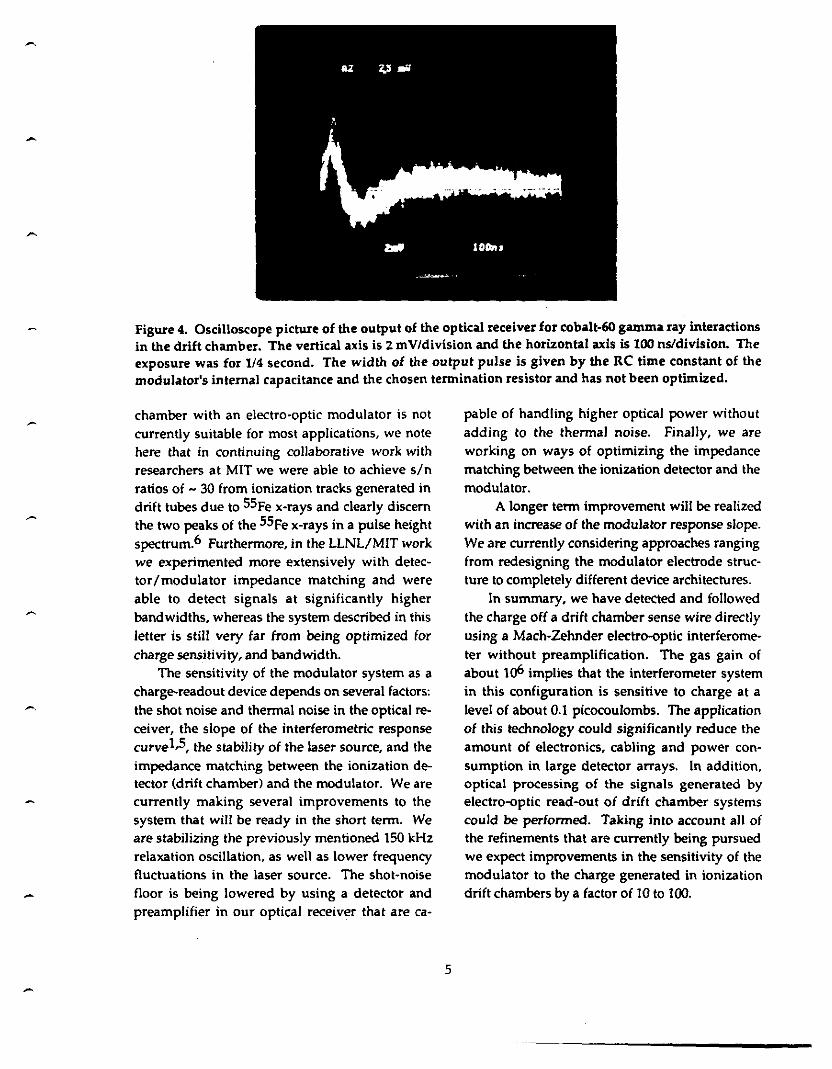
-
Figure 4. Oscilloscope picture of the output of the optical receiver for cobalt-60 gamma ray interactions in the drift chamber. The vertical axis is 2 mV/division and the horizontal axis is 100 ns/division. The exposure was for 1/4 second. The width of the output pulse is given by the RC time constant of the modulator's internal capacitance and the chosen termination resistor and has not been optimized.
chamber with an electro-optic modulator is not currently suitable for most applications, we note here that in continuing collaborative work with researchers at MIT we were able to achieve s/n ratios of - 30 from ionization tracks generated in drift tubes due to 55Fe x-rays and clearly discern the two peaks of the 55Fe x-rays in a pulse height spectrum.6 Furthermore, in the LLNL/MIT work we experimented more extensively with detector /modulator impedance matching and were able to detect signals at significantly higher bandwidths, whereas the system described in this letter is still very far from being optimized for charge sensitivity, and bandwidth.
The sensitivity of the modulator system as a charge-readout device depends on several factors: the shot noise and thermal noise in the optical receiver, the slope of the interferometric response curvel,5, the stability of the laser source, and the impedance matching between the ionization detector (drift chamber) and the modulator. We are currently making several improvements to the system that will be ready in the short term. We are stabilizing the previously mentioned 150 kHz relaxation oscillation, as well as lower frequency fluctuations in the laser source. The shot-noise floor is being lowered by using a detector and preamplifier in our optical receiver that are ca-
5
pable of handling higher optical power without adding to the thermal noise. Finally, we are working on ways of optimizing the impedance matching between the ionization detector and the modulator.
A longer term improvement will be realized with an increase of the modulator response slope. We are currently considering approaches ranging from redesigning the modulator electrode structure to completely different device architectures.
ln summary, we have detected and followed the charge off a drift chamber sense wire directly using a Mach-Zehnder electro-optic interferome· ter without preamplification. The gas gain of about 1o6 implies that the interferometer system in this configuration is sensitive to charge at a level of about 0.1 picocoulombs. The application of this technology could significantly reduce the amount of electronics, cabling and power consumption in large detector arrays. In addition, optical processing of the signals generated by electro-optic read-out of drift chamber systems could be performed. Taking into account all of the refinements that are currently being pursued we expect improvements in the sensitivity of the modulator to the charge generated in ionization drift chambers by a factor of 10 to 100.

Acknowledgements
Work performed under the auspices of the U.S. Department of Energy by the Lawrence Livermore National Laboratory under Contract W-7405-ENG-48.
References
1. M. Lowry, et al., ·An Electro-Optical Approach to the Prompt Signal Processing Problem of Mega-Channel SSC Detector Arrays," UCRL-JC-105645, prepared for submission to the Symposium on Detector Research and Development for the Superconducting Super Collider, Fort Worth, TX, October 15-18, 1990.
2. R. Bionta, et al., "Liquid Scintillator Calorimetry: A Research and Development Proposal," submitted to the Superconducting Super Collider Laboratory, December, 1990 (unpublished).
3. U. Becker, et al., "Resolution Study for Large Drift Chamber Systems," Nucl. Instr. Meth. m pps. 338-342 0984>.
4. D. Antreasyan, et al., "The L3 HighResolution Muon Drift Chambers: Systematic Errors in Track Position Measurements, Nucl. Instr. Meth.~ pps. 304-310 (1986).
5. M. Lowry, et al., "Electro-Optic Transient Imaging Instrumentation Development at Lawrence Livermore National Laboratory: Implications for SSC Instrumentation Development," to be published in the proceedings of the Symposium on Detector Research and Development for the Superconducting Super Collider, Fort Worth, TX, October 15-18, 1990.
6. U. Becker, et al., to be published.
6
--
---
--
--
-
-