Embed Size (px)
Citation preview
© 2007 Nature Publishing Group
Multiscale patterning of plasmonicmetamaterials
JOEL HENZIE1, MIN HYUNG LEE1 AND TERI W. ODOM1,2*1Department of Chemistry, Northwestern University, Evanston, Illinois 60208, USA2Department of Materials Science and Engineering, Northwestern University, Evanston, Illinois 60208, USA
*e-mail: [email protected]
Published online: 19 August 2007; doi:10.1038/nnano.2007.252
The interaction of light with surface plasmons—collectiveoscillations of free electrons—in metallic nanostructureshas resulted in demonstrations of enhanced opticaltransmission1, collimation of light through a subwavelengthaperture2, negative permeability and refraction at visiblewavelengths3,4, and second-harmonic generation frommagnetic metamaterials5. The structures that display theseplasmonic phenomena typically consist of ordered arrays ofparticles or holes with sizes of the order of 100 nm. However,surface plasmons can interact with each other over muchlonger distances, so the ability to organize nanoscale particlesor holes over multiple length scales could lead to newplasmonic metamaterials with novel optical properties6. Here,we present a high-throughput nanofabrication technique—softinterference lithography—that combines the ability ofinterference lithography7 to produce wafer-scale nanopatternswith the versatility of soft lithography8, and use it to createsuch plasmonic metamaterials. Metal films perforated withquasi-infinite arrays of 100-nm holes were generated over areasgreater than 10 cm2, exhibiting sharp spectral features thatchanged in relative amplitude and shifted to longerwavelengths when exposed to increased refractive indexenvironments. Moreover, gold nanohole arrays patternedinto microscale patches exhibited strikingly differenttransmission properties; for instance, patches of nanoholesdisplayed narrow resonances (,14.5 nm full-width-at-half-maximum) that resulted in high refractive index sensitivitiesfar exceeding those reported previously9. Soft interferencelithography was also used to produce various infinite andfinite-area arrays of nanoparticles, including patterns thatcontained optically distinct particles side by side and arraysthat contained both metallic and dielectric materials.
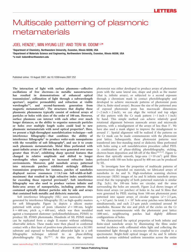
Soft interference lithography (SIL) uses nanoscale patternsgenerated by interference lithography (IL) as high-quality mastersfor soft lithography. Figure 1a depicts a silicon masterpatterned with arrays of posts (diameter d ¼ 100 nm, heighth ¼ 400 nm, pitch a0 ¼ 400 nm), which was then mouldedagainst a transparent elastomer (polydimethylsiloxane, PDMS) toproduce SIL PDMS photomasks. Hundreds of SIL PDMS maskscan be replicated from a single IL-master without exhibitingobservable defects. These masks were then placed in conformalcontact with a thin layer of positive-tone photoresist on a Si(100)substrate and exposed to broadband ultraviolet light in a softlithographic technique referred to as phase-shiftingphotolithography (Fig. 1b)10,11. At this point, the exposed
photoresist was either developed to produce arrays of photoresistposts with the same lateral size, shape and pitch as the master(that is, infinite arrays), or subjected to a second exposurethrough a chromium mask in contact photolithography anddeveloped to achieve microscale patterns of photoresist posts(that is, finite-sized arrays). Because the size of the patterned areaof exposed photoresist posts has macroscale dimensions(�2 inch � 2 inch), we can align the vertical and top edgesof this pattern with the Cr mask pattern (�1 inch � 1 inch)by hand. This simple method can achieve relatively goodrotational alignment between nanoscale arrays and microscalepatterns, with a misalignment of the arrays of less than 58. Wehave also used a mask aligner to improve the misalignment toaround 18. Spatial alignment will be realized if the patterns onthe Cr mask can be made commensurate with the photoresistpost lattice. Subsequently, these photoresist patterns weretransferred into free-standing metal or dielectric films perforatedwith holes using a soft nanofabrication procedure called PEEL(a combination of phase-shifting photolithography, etching,electron-beam deposition and lift-off of the film)10,12,13. Figure 1cshows that optically smooth, large-area (.10 cm2) gold filmsperforated with 100-nm holes spaced by 400 nm can be producedby SIL.
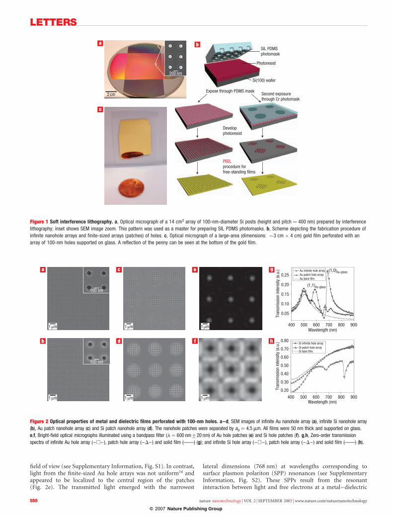
To investigate how the properties of multiscale patterns ofnanostructures depended on materials, we fabricated arrays ofnanoholes in Au and Si. High-resolution scanning electronmicroscopy (SEM) images of Au and Si infinite nanohole arraysreveal that the topography of both patterned materials is similar(Fig. 2a,b); the 100-nm holes are circular, and the areassurrounding the holes are smooth. Figure 2c,d shows images offinite-sized arrays (or patches) of holes in Au and Si films thatwere generated by PEEL starting from 100-nm photoresist postspatterned into square arrays of circular regions (d ¼ 2.5 mm,a0 ¼ 4.5 mm). In total, 1 � 107 hole-array patches were fabricatedsimultaneously, and each 2.5-mm patch contained around 30nanoholes. Because the size and pitch of the circles on the Crmask were incommensurate with the photoresist post lattice(400 nm), neighbouring patches had slightly differentconfigurations of holes.
We characterized the optical properties of both infinite andfinite-sized nanohole arrays by illuminating the films undernormal incidence with collimated white light and collecting thetransmitted light through a microscope objective coupled to aspectrometer. Bright-field optical images of Au and Si infinitenanohole arrays exhibited uniform intensities across the entire
LETTERS
nature nanotechnology | VOL 2 | SEPTEMBER 2007 | www.nature.com/naturenanotechnology 549
© 2007 Nature Publishing Group
field of view (see Supplementary Information, Fig. S1). In contrast,light from the finite-sized Au hole arrays was not uniform14 andappeared to be localized to the central region of the patches(Fig. 2e). The transmitted light emerged with the narrowest
lateral dimensions (768 nm) at wavelengths corresponding tosurface plasmon polariton (SPP) resonances (see SupplementaryInformation, Fig. S2). These SPPs result from the resonantinteraction between light and free electrons at a metal–dielectric
2 cm
200 nm
Photoresist
Si(100) wafer
Developphotoresist
PEELprocedure forfree-standing films
SIL PDMS photomask
Expose through PDMS maskSecond exposure through Cr photomask
Figure 1 Soft interference lithography. a, Optical micrograph of a 14 cm2 array of 100-nm-diameter Si posts (height and pitch ¼ 400 nm) prepared by interference
lithography; inset shows SEM image zoom. This pattern was used as a master for preparing SIL PDMS photomasks. b, Scheme depicting the fabrication procedure of
infinite nanohole arrays and finite-sized arrays (patches) of holes. c, Optical micrograph of a large-area (dimensions: �3 cm � 4 cm) gold film perforated with an
array of 100-nm holes supported on glass. A reflection of the penny can be seen at the bottom of the gold film.
100 nm
1 µm 1 µm1 µm
1 µm 1 µm1 µm
100 nm
h
Tran
smis
sion
inte
nsity
(a.u
.)
400 900800700600500Wavelength (nm)
Si infinite hole array
Si bare film Si patch hole array
0.60
0.40
0.20
0.80
0.30
0.50
0.70
400 900800700600500Wavelength (nm)
Au infinite hole array
Au bare film Au patch hole array
Tran
smis
sion
inte
nsity
(a.u
.) (1,0)Au-glass
(1,1)Au-glass
0.25
0.10
0.05
0.20
0.15
Figure 2 Optical properties of metal and dielectric films perforated with 100-nm holes. a–d, SEM images of infinite Au nanohole array (a), infinite Si nanohole array
(b), Au patch nanohole array (c) and Si patch nanohole array (d). The nanohole patches were separated by a0 ¼ 4.5mm. All films were 50 nm thick and supported on glass.
e,f, Bright-field optical micrographs illuminated using a bandpass filter (l¼ 600 nm+20 nm) of Au hole patches (e) and Si hole patches (f). g,h, Zero-order transmission
spectra of infinite Au hole array (–A–), patch hole array (–D–) and solid film (——) (g); and infinite Si hole array (–A–), patch hole array (–D–) and solid film (——) (h).
LETTERS
nature nanotechnology | VOL 2 | SEPTEMBER 2007 | www.nature.com/naturenanotechnology550
© 2007 Nature Publishing Group
interface. Although the geometries of the Au and Si patches weresimilar, their different material properties resulted in oppositeeffects, with light being concentrated in the former case andsuppressed in the latter (Fig. 2f ).
Figure 2g highlights the differences between the zero-ordertransmission spectra of infinite and finite-sized Au nanoholearrays. The intensity of the bulk plasmon resonance aroundl ¼ 500 nm was similar for all spectra. The infinite nanoholearrays exhibited peaks characteristic of SPP–Bloch waves (BW) atthe Au–glass interface of l(1,0) ¼ 690 nm and l(1,1) ¼ 588 nm(ref. 15), where the subscripts (1,0) and (1,1) are integer pairsthat define the particular order of the SPP–BW. The minimumin the spectra at l ¼ 659 nm can be associated with a Wood’sanomaly (that is, light diffracted parallel to the surface of thefilm)16. Compared with the calculated transmission of hole arraysbased only on geometry, SIL Au nanohole arrays exhibitedenhanced optical transmission factors as large as 11, providingevidence that SIL can produce hole arrays of optical qualitysimilar to those fabricated by focused ion-beam milling1.Strikingly, the spectra of Au patches of nanoholes exhibited amarked decrease in the relative intensity of the (1,0) SPP–BWresonance, which indicated that short-range coupling betweenholes was reduced, and the width of this peak was significantlynarrower than that of the infinite array (full-width-at-half-maximum, FWHM ¼ 18.3 versus 34.1 nm). Moreover, a new,narrow peak emerged at l ¼ 660 nm with a FWHM of 16.8 nm.In contrast, infinite Si nanohole arrays showed decreasedtransmission compared with solid films, and finite-sized arraysexhibited transmission slightly less than bare films (Fig. 2 h).Despite the different hole arrangements of individual patches, the
spectra from single patches were identical because theycontained, on average, the same number of holes.
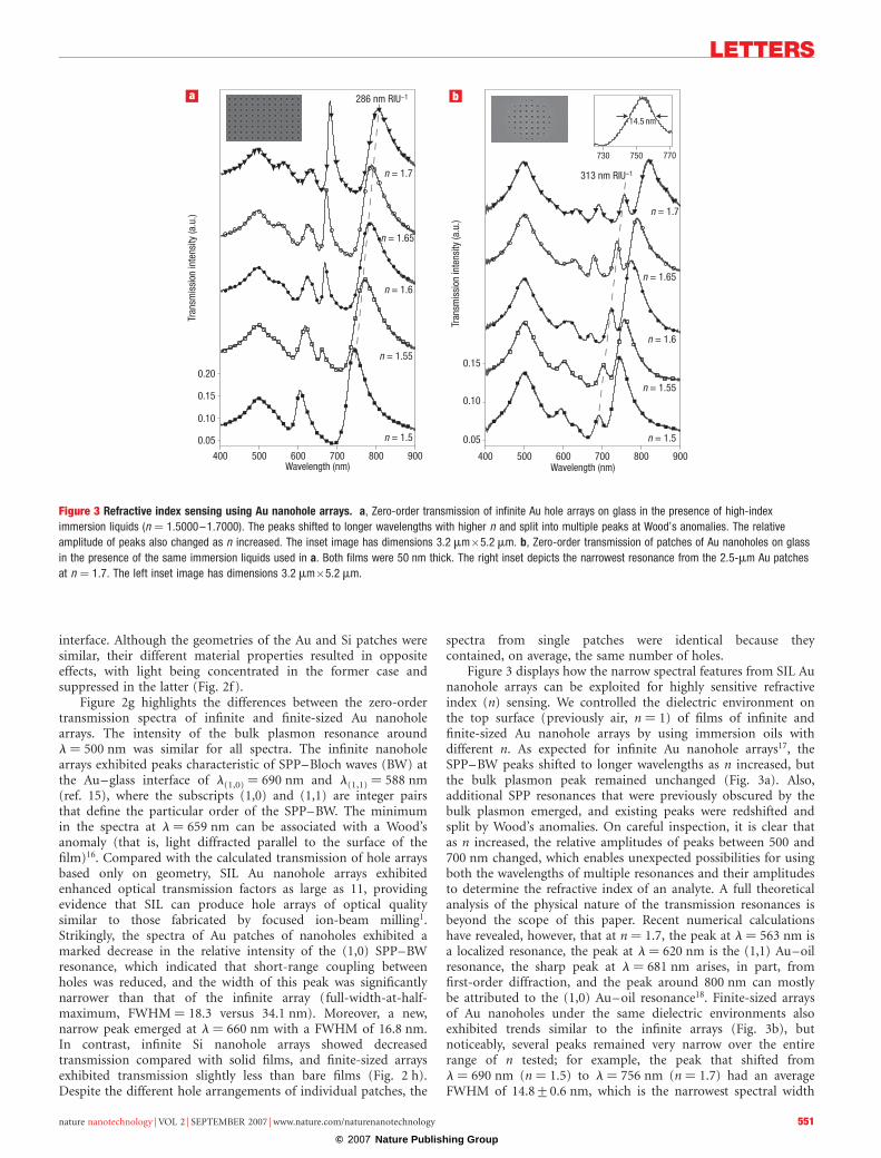
Figure 3 displays how the narrow spectral features from SIL Aunanohole arrays can be exploited for highly sensitive refractiveindex (n) sensing. We controlled the dielectric environment onthe top surface (previously air, n ¼ 1) of films of infinite andfinite-sized Au nanohole arrays by using immersion oils withdifferent n. As expected for infinite Au nanohole arrays17, theSPP–BW peaks shifted to longer wavelengths as n increased, butthe bulk plasmon peak remained unchanged (Fig. 3a). Also,additional SPP resonances that were previously obscured by thebulk plasmon emerged, and existing peaks were redshifted andsplit by Wood’s anomalies. On careful inspection, it is clear thatas n increased, the relative amplitudes of peaks between 500 and700 nm changed, which enables unexpected possibilities for usingboth the wavelengths of multiple resonances and their amplitudesto determine the refractive index of an analyte. A full theoreticalanalysis of the physical nature of the transmission resonances isbeyond the scope of this paper. Recent numerical calculationshave revealed, however, that at n ¼ 1.7, the peak at l ¼ 563 nm isa localized resonance, the peak at l ¼ 620 nm is the (1,1) Au–oilresonance, the sharp peak at l ¼ 681 nm arises, in part, fromfirst-order diffraction, and the peak around 800 nm can mostlybe attributed to the (1,0) Au–oil resonance18. Finite-sized arraysof Au nanoholes under the same dielectric environments alsoexhibited trends similar to the infinite arrays (Fig. 3b), butnoticeably, several peaks remained very narrow over the entirerange of n tested; for example, the peak that shifted froml ¼ 690 nm (n ¼ 1.5) to l ¼ 756 nm (n ¼ 1.7) had an averageFWHM of 14.8+0.6 nm, which is the narrowest spectral width
900800700600500Wavelength (nm)
400
Tran
smis
sion
inte
nsity
(a.u
.)
n = 1.7
n = 1.5
n = 1.55
n = 1.6
n = 1.65
286 nm RIU–1
0.20
0.15
0.10
0.05
Wavelength (nm)900800700600500400
Tran
smis
sion
inte
nsity
(a.u
.)
n = 1.7
n = 1.5
n = 1.55
n = 1.6
n = 1.65
313 nm RIU–1
0.15
0.10
0.05
730 750 770
14.5 nm
Figure 3 Refractive index sensing using Au nanohole arrays. a, Zero-order transmission of infinite Au hole arrays on glass in the presence of high-index
immersion liquids (n ¼ 1.5000–1.7000). The peaks shifted to longer wavelengths with higher n and split into multiple peaks at Wood’s anomalies. The relative
amplitude of peaks also changed as n increased. The inset image has dimensions 3.2 mm�5.2 mm. b, Zero-order transmission of patches of Au nanoholes on glass
in the presence of the same immersion liquids used in a. Both films were 50 nm thick. The right inset depicts the narrowest resonance from the 2.5-mm Au patches
at n ¼ 1.7. The left inset image has dimensions 3.2 mm�5.2 mm.
LETTERS
nature nanotechnology | VOL 2 | SEPTEMBER 2007 | www.nature.com/naturenanotechnology 551
© 2007 Nature Publishing Group
reported to date for a surface plasmon resonance excited using anincoherent light source.
One strategy to compare the sensitivity of different metallicnanostructure systems for refractive index sensing is to calculatetheir figure of merit (FOM), which is the shift per refractiveindex unit (RIU) divided by the width of the surface plasmonresonance (calculated in units of eV)19. The SPP–BW peaksfor the infinite Au nanohole arrays were relatively broad(FWHM ¼ 70 nm), and with a shift of 286 nm RIU21, thehighest FOM achieved was � 4.1 for the l(1,0) resonance(Fig. 3a). The resonances for the Au patches shifted slightly morethan the infinite array (313 nm RIU21; or 0.747 eV RIU21), andconsidering the peak nearest to l(1,0) (whose FWHM ¼ 14.5 nmat n ¼ 1.7; or 0.032 eV), a FOM as large as 23.3 was produced.This value far exceeds the range reported for metal nanoparticles(FOM ¼ 0.9–5.4; ref. 9) as well as that of a recently reported
structure made from a metal film deposited over polystyrenespheres20. Surprisingly, the best architecture for arrays of patchesfor refractive-index sensing consisted of patches that were closeenough (for example, a0 ¼ 4.5 mm) to interact with each other.Patches of similar and larger sizes (2.5, 5 and 10 mm) separatededge to edge by 15 mm (that is, a0 ¼ 17.5–25 mm), a distancegreater than the Au-plasmon decay length, did not support anynew resonances. Significantly, as the number of holes increased,the patches began to exhibit features characteristic of the infinitearray (see Supplementary Information, Figs S3 and S4).
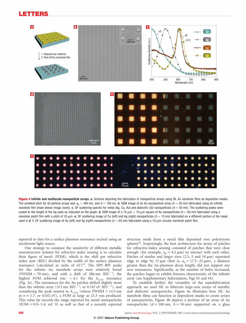
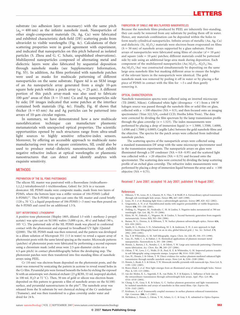
To establish further the versatility of the nanofabricationapproach, we used SIL to fabricate large-area arrays of metallicand dielectric nanoparticles. Figure 4a illustrates how SIL Aunanohole films can function as deposition masks to create arraysof nanoparticles. Figure 4b depicts a portion of an array of Aunanoparticles (d ¼ 100 nm, h ¼ 50 nm) supported on a glass
400 nm
200 nm
1. Deposit any material2. Peel off Au nanohole film
10 µm2 µm
20 µm
x8 x5
x3.5
Scat
terin
g in
tens
ity (a
.u.)
900800700600500400Wavelength (nm)
Si
Ag
Cu
Au
Figure 4 Infinite and multiscale nanoparticle arrays. a, Scheme depicting the fabrication of nanoparticle arrays using SIL Au nanohole films as deposition masks.
The smallest pitch for all particle arrays was a0 ¼ 400 nm, and d ¼ 100 nm. b, SEM image of an Au nanoparticle array (h ¼ 50 nm) fabricated using an infinite
nanohole film (inset shows image zoom). c, DF scattering spectra for metal (Ag, Cu, Au) and dielectric (Si) nanoparticles (h ¼ 50 nm). The scattering peaks were
scaled to the height of the Ag peak as indicated on the graph. d, SEM image of a 10 mm � 10 mm square of Au nanoparticles (h ¼ 65 nm) fabricated using a
nanohole patch film with a pitch of 25 mm. e, DF scattering image of Cu (left) and Ag (right) nanoparticles (h ¼ 15 nm) fabricated on a different portion of the mask
used in d. f, DF scattering image of Au (left) and Ag (right) nanoparticles (h ¼ 65 nm) fabricated using a 10-mm circular nanohole patch film.
LETTERS
nature nanotechnology | VOL 2 | SEPTEMBER 2007 | www.nature.com/naturenanotechnology552
© 2007 Nature Publishing Group
substrate (no adhesion layer is necessary) with the same pitch(a0 ¼ 400 nm) as the infinite nanohole mask. Nanoparticles ofother single-component materials (Si, Ag, Cu) were fabricatedand exhibited characteristic dark-field (DF) scattering peaks fromultraviolet to visible wavelengths (Fig. 4c). Calculations of theirscattering properties were in good agreement with experiment,and indicated that nanoparticles on this pitch behaved as isolatedparticles (S. Zhou and G. C. Schatz, unpublished observations).Multilayered nanoparticles composed of alternating metal anddielectric layers were also fabricated by sequential depositionthrough nanohole masks (see Supplementary Information,Fig. S5). In addition, Au films perforated with nanohole patcheswere used as masks for multiscale patterning of differentnanoparticles on the same substrate. Figure 4d is an SEM imageof an Au nanoparticle array generated from a single 10-mmsquare hole patch within a patch array (a0 ¼ 25 mm). A differentportion of this patch array-mask was also used to fabricate100-mm2 areas of thin (h ¼ 15 nm) Cu and Ag nanoparticles sideby side; DF images indicated that some patches at the interfacecontained both materials (Fig. 4e). Finally, Fig. 4f shows thatthicker (h ¼ 65 nm) Au and Ag particles can be patterned intoarrays of 10-mm circular regions.
In summary, we have demonstrated how a new multiscalenanofabrication technique can manufacture plasmonicmetamaterials with unexpected optical properties. The scientificopportunities opened by such structures range from ultra-smalllight sources to highly sensitive refractive-index sensors.Moreover, by offering an accessible approach to multiscale nanomanufacturing over tens of square centimetres, SIL could also beused to produce metal–dielectric nanostructures that exhibitnegative refractive indices at optical wavelengths or plasmonicnanostructures that can detect and identify analytes withexquisite sensitivity.
METHODS
PREPARATION OF THE SIL PDMS PHOTOMASKS
The silicon SIL master was passivated with a fluorosilane (tridecafluoro-1,1,2,2-tetrahydrooctyl-1-trichlorosilane, Gelest) for 24 h in a vacuumdessicator. SIL PDMS masks were composite masks, made from two layers ofPDMS, where the bottom layer was a stiffer version of 184-PDMS (calledh-PDMS)11. The h-PDMS was spin-cast onto the SIL master and cured briefly(120 s, 70 8C); a liquid prepolymer of 184-PDMS (�3 mm) was then poured onthe h-PDMS and cured for an additional 1.5 h.
SOFT INTERFERENCE LITHOGRAPHY
A positive-tone photoresist (Shipley 1805, diluted 1:3 with 1-methoxy-2-propylacetate) was spin-cast on Si(100) wafers (5,000 r.p.m., 40 s) and baked (90 s,105 8C). The patterned side of the SIL PDMS mask was placed in conformalcontact with the photoresist and exposed to broadband UV light (QuintelQ2000). The SIL PDMS mask was then removed, and the pattern was developedin a dilute solution of Microposit 351 (1:5 in water) to reveal a square array ofphotoresist posts with the same lateral spacing as the master. Microscale patterns(patches) of photoresist posts were fabricated by performing a second exposureusing a chromium mask (solid areas were 2.5-mm-diameter circles on a4.5-mm pitch) in contact photolithography before the developing step. Thephotoresist patches were then transferred into free-standing films of nanoholearrays using PEEL.
Cr (10 nm) was electron-beam deposited on the photoresist posts, and theresist was removed by sonicating the pattern in acetone to reveal round holes inthe Cr film. Pyramidal pits were formed beneath the holes by etching the exposedSi with an anisotropic wet chemical etchant (23 g KOH, 33 mL isopropyl alcohol,in 100 mL H2O at 72 8C). Then, 50 nm of gold or silicon was electron-beamdeposited on this pattern to generate a film of nanohole arrays on the Si(100)surface, and pyramidal nanostructures in the pits13. The nanohole array wasreleased from the Si substrate by wet chemical etching of the Cr underlayer(Transene), and was then transferred to a glass coverslip under water anddried for 24 h.
FABRICATION OF SINGLE AND MULTILAYERED NANOPARTICLES
Because the nanohole films produced by PEEL are inherently free-standing,they can easily be removed from any substrate by peeling them off in water.Hence, any materials combination can be deposited within the holes toform nearly cylindrical nanoparticles. Infinite arrays of metallic (Au, Ag, Cu)and dielectric (Si, Al2O3) materials were electron-beam evaporated on films(h ¼ 50 nm) of nanohole arrays supported by a glass substrate. Finitearrays of nanoparticles were fabricated using films of circular (d ¼ 10 mm)and square (side ¼ 10 mm) patches; different materials could be patternedside by side using an additional large-area mask during deposition. Eachcomponent of the multilayered nanoparticles (Au/Al2O3, Al2O3/Au,Au/Al2O3/Au) was constructed simultaneously by depositing on the samelarge-area nanohole film but masking different areas to ensure the heightsof the relevant layers in the nanoparticle were identical. The goldnanohole mask was removed by peeling it off in water or by placing a flatpiece of PDMS in contact with the film for �5 s and then gentlyremoving it.
OPTICAL CHARACTERIZATION
Nanohole transmission spectra were collected using an inverted microscope(TE-2000U, Nikon). Collimated white light (divergence ,48) from a 100 Whalogen source was passed through the nanohole film or solid film on glass,collected with a �100 objective (NA ¼ 0.5), and then focused onto an imagingspectrometer (Triax 522/LN2-cooled CCD, Horiba Jobin Yvon). The datawere corrected by dividing the film spectrum by the lamp transmission profilethrough the glass coverslip (n ¼ 1.523). The index measurements wereperformed by placing a drop of immersion liquid (n ¼ 1.5000, 1.5500, 1.6000,1.6500 and 1.7000+0.0005; Cargille Labs) between the gold nanohole films andthe objective. The spectra for the patch arrays were collected from individualnanohole patches.
The scattering spectra of the nanoparticle arrays were collected usinga standard transmission DF setup with the same microscope spectrometer usedin the transmission experiments. The nanoparticle arrays on glass wereilluminated through a DF condenser (NA ¼ 0.8–0.95) and the scattered lightwas collected with a �20 objective (NA ¼ 0.75) and focused onto thespectrometer. The scattering data were corrected by dividing the lamp scatteringprofile of an etched glass coverslip. The refractive index measurements wereperformed by placing a drop of immersion liquid between the array and a �100objective (NA ¼ 0.75).
Received 7 June 2007; accepted 16 July 2007; published 19 August 2007.
References1. Ebbesen, T. W., Lezec, H. J., Ghaemi, H. F., Thio, T. & Wolff, P. A. Extraordinary optical transmission
through sub-wavelength hole arrays. Nature 391, 667–669 (1998).2. Lezec, H. J. et al. Beaming light from a subwavelength aperture. Science 297, 820–822 (2002).3. Grigorenko, A. N. et al. Nanofabricated media with negative permeability at visible frequencies.
Nature 438, 335–338 (2005).4. Dolling, G., Wegener, M., Soukoulis, C. M. & Linden, S. Negative-index metamaterial at 780 nm
wavelength. Opt. Lett. 32, 53–55 (2006).5. Klein, M. W., Enkrich, C., Wegener, M. & Linden, S. Second-harmonic generation from magnetic
metamaterials. Science 313, 502–504 (2006).6. Barnes, W. L., Dereux, A. & Ebbesen, T. W. Surface plasmon subwavelength optics. Nature 424,
824–830 (2003).7. Smith, H. I., Hector, S. D., Schattenburg, M. L. & Anderson, E. H. A new approach to high
fidelity e-beam lithography based on an in-situ, global fiducial grid. J. Vac. Sci. Technol. B 9,2992–2995 (1991).
8. Xia, Y. & Whitesides, G. M. Soft lithography. Angew. Chem. Int. Edn 37, 550–575 (1998).9. Liao, H., Nehl, C. L. & Hafner, J. H. Biomedical applications of plasmon resonant metal
nanoparticles. Nanomedicine 1, 201–208 (2006).10. Henzie, J., Barton, J. E., Stender, C. L. & Odom, T. W. Large-area nanoscale patterning: Chemistry
meets fabrication. Acc. Chem. Res. 39, 249–257 (2006).11. Odom, T. W., Love, J. C., Wolfe, D. B., Paul, K. E. & Whitesides, G. M. Improved pattern transfer
in soft lithography using composite stamps. Langmuir 18, 5314–5320 (2002).12. Gao, H., Henzie, J. & Odom, T. W. Direct evidence for surface plasmon-mediated enhanced light
transmission through metallic nanohole arrays. Nano Lett. 6, 2104–2108 (2006).13. Henzie, J., Kwak, E. S. & Odom, T. W. Mesoscale metallic pyramids with nanoscale tips. Nano Lett. 5,
1199–1202 (2005).14. Bravo-Abad, J. et al. How light emerges from an illuminated array of subwavelength holes. Nature
Phys. 2, 120–123 (2006).15. van der Molen, K. L., Segerink, F. B., van Hulst, N. F. & Kuipers, L. Influence of hole size on
the extraordinary transmission through subwavelength hole arrays. Appl. Phys. Lett. 85,4316–4318 (2004).
16. Chang, S.-H., Gray, S. K. & Schatz, G. C. Surface plasmon generation and light transmissionby isolated nanoholes and arrays of nanoholes in thin metal films. Opt. Express 13,3150 –3165 (2005).
17. Krishnan, A. et al. Evanescently coupled resonance in surface plasmon enhanced transmission.Opt. Commun. 200, 1–7 (2001).
18. McMahon, J., Henzie, J., Odom, T. W., Schatz, G. C. & Gray, S. K. submitted to Optics Express.
LETTERS
nature nanotechnology | VOL 2 | SEPTEMBER 2007 | www.nature.com/naturenanotechnology 553

© 2007 Nature Publishing Group
19. Sherry, L. J. et al. Localized surface plasmon resonance spectroscopy of single silver nanocubes.Nano Lett. 5, 2034–2038 (2005).
20. Hicks, E. M. et al. Plasmonic properties of film over nanowell surfaces fabricated by nanospherelithography. J. Phys. Chem. B 109, 22351–22358 (2005).
AcknowledgementsThis work was supported by the National Science Foundation (NSF) under NSF Award NumberDMR-0632947 and the MRSEC program at the Materials Research Center under NSF Award NumberDMR-0520513. This work made use of the NUANCE Center facilities, which are supported byNSF-MRSEC, NSF-NSEC and the Keck Foundation. We thank T. A. Savas and H. I. Smith for the Simasters made by interference lithography. We thank G. C. Schatz, S. K. Gray and J. McMahon for manydiscussions. T.W.O. is a DuPont Young Professor, an Alfred P. Sloan Research Fellow, a Cottrell Scholar ofResearch Corporation, and a David and Lucile Packard Fellow.
Correspondence and requests for materials should be addressed to T.W.O.Supplementary information accompanies this paper on www.nature.com/naturenanotechnology.
Author contributionsJ.H. and M.H.L. performed the experiments. J.H., M.H.L. and T.W.O. designed the experiments, analysedthe results and co-wrote the manuscript.
Competing financial interestsThe authors declare no competing financial interests.
Reprints and permission information is available online at http://npg.nature.com/reprintsandpermissions/
LETTERS
nature nanotechnology | VOL 2 | SEPTEMBER 2007 | www.nature.com/naturenanotechnology554


![Enhancing the Angular Sensitivity of Plasmonic Sensors ...biotheory.phys.cwru.edu/PDF/AOM.pdf · ultrasensitive plasmonic biosensors.[29,30] A plasmonic nanorod metamaterial (Type](https://img.pdfslide.us/doc/110x75/5fcdd2c6db367d06a677e7be/enhancing-the-angular-sensitivity-of-plasmonic-sensors-ultrasensitive-plasmonic.jpg)