Embed Size (px)
Citation preview
Multiple Range, 16-/12-Bit, Bipolar/Unipolar, Voltage Output DACs
Data Sheet AD5761/AD5721
Rev. C Document Feedback Information furnished by Analog Devices is believed to be accurate and reliable. However, no responsibility is assumed by Analog Devices for its use, nor for any infringements of patents or other rights of third parties that may result from its use. Specifications subject to change without notice. No license is granted by implication or otherwise under any patent or patent rights of Analog Devices. Trademarks and registered trademarks are the property of their respective owners.
One Technology Way, P.O. Box 9106, Norwood, MA 02062-9106, U.S.A.Tel: 781.329.4700 ©2015–2018 Analog Devices, Inc. All rights reserved. Technical Support www.analog.com
FEATURES 8 software-programmable output ranges: 0 V to +5 V, 0 V to
+10 V, 0 V to +16 V, 0 V to +20 V, ±3 V, ±5 V, ±10 V, −2.5 V to +7.5 V; 5% overrange
Total unadjusted error (TUE): 0.1% FSR maximum 16-bit resolution: ±2 LSB maximum INL Guaranteed monotonicity: ±1 LSB maximum Single channel, 16-/12-bit DACs Settling time: 7.5 μs typical Integrated reference buffers Low noise: 35 nV/√Hz Low glitch: 1 nV-sec 1.8 V logic compatibility Asynchronous updating via LDAC Asynchronous RESET to zero scale/midscale DSP/microcontroller-compatible serial interface Robust 4 kV HBM ESD rating Available in 16-lead TSSOP and 16-lead LFCSP Operating temperature range: −40°C to +125°C
APPLICATIONS Industrial automation Instrumentation, data acquisition Open-/closed-loop servo control, process control Programmable logic controllers
GENERAL DESCRIPTION The AD5761/AD5721 are single channel, 16-/12-bit serial input, voltage output, digital-to-analog converters (DACs). They operate from single supply voltages from +4.75 V to +30 V or dual supply voltages from −16.5 V to 0 V VSS and +4.75 V to +16.5 V VDD. The integrated output amplifier and reference buffer provide a very easy to use, universal solution.
The devices offer guaranteed monotonicity, integral nonlinearity (INL) of ±2 LSB maximum, 35 nV/√Hz noise, and 7.5 μs settling time on selected ranges.
The AD5761/AD5721 use a serial interface that operates at clock rates of up to 50 MHz and are compatible with DSP and microcontroller interface standards. Double buffering allows the asynchronous updating of the DAC output. The input coding is user-selectable twos complement or straight binary. The asynchronous reset function resets all registers to their default state. The output range is user selectable, via the RA[2:0] bits in the control register.
The devices available in the 16-lead TSSOP and in the 16-lead LFCSP offer guaranteed specifications over the −40°C to +125°C industrial temperature range.
Table 1. Pin-Compatible Devices Device Description AD5761R/AD5721R AD5761/AD5721 with internal reference
FUNCTIONAL BLOCK DIAGRAM
12-BIT/16-BITDAC
LDAC
VOUT
REFERENCEBUFFERS
SDISCLK
SYNC
SDO
RESET
VDD
VSS
DVCC
INPUT SHIFTREGISTER
ANDCONTROL
LOGIC
DGND AGND
AD5761/AD5721
CLEAR
INPUTREG
DACREG
12/1612/16
ALERT
VREFIN
DNC
1264
0-00
1
0V TO 5V0V TO 10V0V TO 16V0V TO 20V±3V±5V±10V−2.5V TO +7.5V
NOTES1. DNC = DO NOT CONNECT. DO NOT CONNECT TO THIS PIN.
Figure 1.
AD5761/AD5721 Data Sheet
Rev. C | Page 2 of 31
TABLE OF CONTENTS Features .............................................................................................. 1 Applications ....................................................................................... 1 General Description ......................................................................... 1 Functional Block Diagram .............................................................. 1 Revision History ............................................................................... 2 Specifications ..................................................................................... 3
AC Performance Characteristics ................................................ 5 Timing Characteristics ................................................................ 6
Absolute Maximum Ratings ............................................................ 8 ESD Caution .................................................................................. 8
Pin Configurations and Function Descriptions ........................... 9 Typical Performance Characterstics............................................. 10 Terminology .................................................................................... 20 Theory of Operation ...................................................................... 21
Digital-to-Analog Converter .................................................... 21 Transfer Function ....................................................................... 21 DAC Architecture ....................................................................... 21 Serial Interface ............................................................................ 22 Hardware Control Pins .............................................................. 22
Register Details ............................................................................... 24 Input Shift Register .................................................................... 24 Control Register ......................................................................... 24 Readback Control Register ....................................................... 26 Update DAC Register from Input Register ............................. 26 Readback DAC Register ............................................................ 26 Write and Update DAC Register .............................................. 27 Readback Input Register ............................................................ 27 Disable Daisy-Chain Functionality .......................................... 27 Software Data Reset ................................................................... 28 Software Full Reset ..................................................................... 28 No Operation Registers ............................................................. 28
Applications Information .............................................................. 29 Typical Operating Circuit ......................................................... 29 Power Supply Considerations ................................................... 29 Evaluation Board ........................................................................ 29
Outline Dimensions ....................................................................... 31 Ordering Guide .......................................................................... 31
REVISION HISTORY 1/2018—Rev. B to Rev. C Changes to Transfer Function Section ......................................... 21 Change to DB[15:11] Column, Table 11 ..................................... 24 Change to RA[2:0] Description, Table 12 ................................... 25 Change to DB[15:13] Column, Table 15 ..................................... 26 Updated Outline Dimensions ....................................................... 31 Changes to Ordering Guide .......................................................... 31 4/2016—Rev. A to Rev. B Changes to Features Section............................................................ 1 Changes to Typical Operating Circuit Section and Precision Voltage Reference Section ............................................................. 29
5/2015—Rev. 0 to Rev. A Added 16-Lead LFCSP Package ....................................... Universal Added Grade A Parameter, Table 2 ................................................. 3 Added Figure 5, Renumbered Sequentially ................................... 9 Changes to Table 6 ............................................................................. 9 Changes to Figure 49 ...................................................................... 17 Changes to Power Supply Considerations Section .................... 30 Updated Outline Dimensions ....................................................... 32 Changes to Ordering Guide .......................................................... 32
1/2015—Revision 0: Initial Version

Data Sheet AD5761/AD5721
Rev. C | Page 3 of 31
SPECIFICATIONS VDD
1 = 4.75 V to 30 V, VSS1 = −16.5 V to 0 V, AGND = DGND = 0 V, VREFIN = 2.5 V external, DVCC = 1.7 V to 5.5 V, RLOAD = 1 kΩ for all
ranges except 0 V to 16 V and 0 V to 20 V for which RLOAD = 2 kΩ, CLOAD = 200 pF, all specifications TMIN to TMAX, unless otherwise noted.
Table 2. Parameter2 Min Typ Max Unit Test Conditions/Comments STATIC PERFORMANCE External reference3, outputs unloaded
Programmable Output Ranges 0 5 V 0 10 V 0 16 V 0 20 V −2.5 +7.5 V −3 +3 V −5 +5 V −10 +10 V AD5761
Resolution 16 Bits Relative Accuracy, INL
A Grade −8 +8 LSB External reference3 B Grade4 −2 +2 LSB All ranges except 0 V to 16 V and 0 V to 20 V, VREFIN =
2.5 V external reference Differential Nonlinearity, DNL −1 +1 LSB
AD5721 Resolution 12 Bits Relative Accuracy, INL
B Grade −0.5 +0.5 LSB External reference3 Differential Nonlinearity, DNL −0.5 +0.5 LSB
Zero-Scale Error −6 +6 mV All ranges except ±10 V and 0 V to 20 V, external reference3
−10 +10 mV 0 V to 20 V, ±10 V ranges, external reference3 Zero-Scale Temperature
Coefficient (TC)5 ±5 µV/°C Unipolar ranges, external reference3
±15 µV/°C Bipolar ranges, external reference3 Bipolar Zero Error −5 +5 mV All bipolar ranges except ±10 V −7 +7 mV ±10 V output range Bipolar Zero TC5 ±2 µV/°C ±3 V range, external reference3 ±5 µV/°C All bipolar ranges except ±3 V, external reference3 Offset Error −6 +6 mV All ranges except ±10 V and 0 V to 20 V, external
reference3 −10 +10 mV 0 V to 20 V, ±10 V ranges; external reference3 Offset Error TC5 ±5 µV/°C Unipolar ranges, external reference3 ±15 µV/°C Bipolar ranges, external reference3 Gain Error −0.1 +0.1 % FSR External reference3 Gain Error TC5 ±1.5 ppm FSR/°C External reference3 Total Unadjusted Error (TUE) −0.1 +0.1 % FSR External reference3
REFERENCE INPUT5 Reference Input Voltage (VREF) 2.5 V ±1% for specified performance Input Current −2 ±0.5 +2 µA Reference Range 2 3 V
OUTPUT CHARACTERISTICS5 Output Voltage Range −VOUT +VOUT Refer to Table 7 for the different output voltage
ranges available −10 +10 V VDD/VSS = ±11 V, ±10 V output range −10.5 +10.5 V VDD/VSS = ±11 V, ±10 V output range with 5%
overrange

AD5761/AD5721 Data Sheet
Rev. C | Page 4 of 31
Parameter2 Min Typ Max Unit Test Conditions/Comments Capacitive Load Stability 1 nF Headroom 0.5 1 V RLOAD = 1 kΩ for all ranges except 0 V to16 V and 0 V
to 20 V ranges (RLOAD = 2 kΩ) Output Voltage TC ±3 ppm FSR/°C ±10 V range, external reference Short-Circuit Current 25 mA Short on the VOUT pin Resistive Load 1 kΩ All ranges except 0 V to16 V and 0 V to 20 V 2 kΩ 0 V to16 V, 0 V to 20 V ranges Load Regulation 0.3 mV/mA Outputs unloaded DC Output Impedance 0.5 Ω Outputs unloaded
LOGIC INPUTS5 DVCC = 1.7 V to 5.5 V, JEDEC compliant Input Voltage
High, VIH 0.7 × DVCC V Low, VIL 0.3 × DVCC V
Input Current Leakage Current −1 +1 µA SDI, SCLK, SYNC
−1 +1 µA LDAC, CLEAR, RESET pins held high
−55 µA LDAC, CLEAR, RESET pins held low
Pin Capacitance 5 pF Per pin, outputs unloaded LOGIC OUTPUTS (SDO, ALERT)5
Output Voltage Low, VOL 0.4 V DVCC = 1.7 V to 5.5 V, sinking 200 µA High, VOH DVCC − 0.5 V DVCC = 1.7 V to 5.5 V, sourcing 200 µA
High Impedance, SDO Pin Leakage Current −1 +1 µA
Pin Capacitance 5 pF POWER REQUIREMENTS
VDD 4.75 30 V VSS −16.5 0 V DVCC 1.7 5.5 V IDD 5.1 6.5 mA Outputs unloaded, external reference ISS 1 3 mA Outputs unloaded DICC 0.005 1 µA VIH = DVCC, VIL = DGND Power Dissipation 67.1 mW ±11 V operation, outputs unloaded DC Power Supply Rejection
Ratio (PSRR)5 0.1 mV/V VDD ± 10%, VSS = −15 V
0.1 mV/V VSS ±10%, VDD = +15 V AC PSRR5 80 dB VDD ±200 mV, 50 Hz/60 Hz, VSS = −15 V; external
reference; CLOAD = unloaded 80 dB VSS ±200 mV, 50 Hz/60 Hz, VDD = +15 V; external
reference; CLOAD = unloaded 1 For specified performance, headroom requirement is 1 V. 2 Temperature range: −40°C to +125°C, typical at +25°C. 3 External reference means 2 V to 2.85 V with overrange and 2 V to 3 V without overrange. 4 Integral nonlinearity error is specified at ±4 LSB (minimum/maximum) for 0 V to 16 V and 0 V to 20 V ranges with VREFIN = 2.5 V external reference, and for all ranges
with VREFIN = 2 V to 2.85 V with overrange and 2 V to 3 V without overrange. 5 Guaranteed by design and characterization, not production tested.
Data Sheet AD5761/AD5721
Rev. C | Page 5 of 31
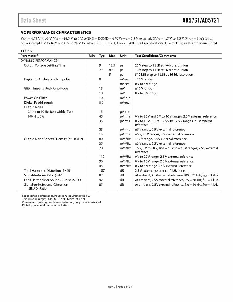
AC PERFORMANCE CHARACTERISTICS VDD
1 = 4.75 V to 30 V, VSS1= −16.5 V to 0 V, AGND = DGND = 0 V, VREFIN = 2.5 V external, DVCC = 1.7 V to 5.5 V, RLOAD = 1 kΩ for all
ranges except 0 V to 16 V and 0 V to 20 V for which RLOAD = 2 kΩ, CLOAD = 200 pF, all specifications TMIN to TMAX, unless otherwise noted.
Table 3. Parameter2 Min Typ Max Unit Test Conditions/Comments DYNAMIC PERFORMANCE3
Output Voltage Settling Time 9 12.5 µs 20 V step to 1 LSB at 16-bit resolution 7.5 8.5 µs 10 V step to 1 LSB at 16-bit resolution 5 µs 512 LSB step to 1 LSB at 16-bit resolution Digital-to-Analog Glitch Impulse 8 nV-sec ±10 V range 1 nV-sec 0 V to 5 V range Glitch Impulse Peak Amplitude 15 mV ±10 V range 10 mV 0 V to 5 V range Power-On Glitch 100 mV p-p Digital Feedthrough 0.6 nV-sec Output Noise
0.1 Hz to 10 Hz Bandwidth (BW) 15 µV p-p 100 kHz BW 45 µV rms 0 V to 20 V and 0 V to 16 V ranges, 2.5 V external reference 35 µV rms 0 V to 10 V, ±10 V, −2.5 V to +7.5 V ranges, 2.5 V external
reference 25 µV rms ±5 V range, 2.5 V external reference 15 µV rms +5 V, ±3 V ranges; 2.5 V external reference
Output Noise Spectral Density (at 10 kHz) 80 nV/√Hz ±10 V range, 2.5 V external reference 35 nV/√Hz ±3 V range, 2.5 V external reference 70 nV/√Hz ±5 V, 0 V to 10 V, and −2.5 V to +7.5 V ranges; 2.5 V external
reference 110 nV/√Hz 0 V to 20 V range, 2.5 V external reference 90 nV/√Hz 0 V to 16 V range, 2.5 V external reference 45 nV/√Hz 0 V to 5 V range, 2.5 V external reference Total Harmonic Distortion (THD)4 −87 dB 2.5 V external reference, 1 kHz tone Signal-to-Noise Ratio (SNR) 92 dB At ambient, 2.5 V external reference, BW = 20 kHz, fOUT = 1 kHz Peak Harmonic or Spurious Noise (SFDR) 92 dB At ambient, 2.5 V external reference, BW = 20 kHz, fOUT = 1 kHz Signal-to-Noise-and-Distortion
(SINAD) Ratio 85 dB At ambient, 2.5 V external reference, BW = 20 kHz, fOUT = 1 kHz
1 For specified performance, headroom requirement is 1 V. 2 Temperature range: −40°C to +125°C, typical at +25°C. 3 Guaranteed by design and characterization; not production tested. 4 Digitally generated sine wave at 1 kHz.

AD5761/AD5721 Data Sheet
Rev. C | Page 6 of 31
TIMING CHARACTERISTICS DVCC = 1.7 V to 5.5 V, all specifications TMIN to TMAX, unless otherwise noted.
Table 4. Parameter Limit at TMIN to TMAX Unit Description t1
1 20 ns min SCLK cycle time t2 10 ns min SCLK high time t3 10 ns min SCLK low time t4 15 ns min SYNC falling edge to SCLK falling edge setup time
t5 10 ns min SCLK falling edge to SYNC rising edge time
t6 20 ns min Minimum SYNC high time (write mode)
t7 5 ns min Data setup time t8 5 ns min Data hold time t9 10 ns min LDAC falling edge to SYNC falling edge
t10 20 ns min SYNC rising edge to LDAC falling edge
t11 20 ns min LDAC pulse width low
t12 9 µs typ DAC output settling time, 20 V step to 1 LSB at 16-bit resolution (see Table 3) 7.5 µs typ DAC output settling time, 10 V step to 1 LSB at 16-bit resolution t13 20 ns min CLEAR pulse width low
t14 200 ns typ CLEAR pulse activation time
t15 10 ns min SYNC rising edge to SCLK falling edge
t16 40 ns max SCLK rising edge to SDO valid (CL_SDO = 15 pF, where CL_SDO is the capacitive load on the SDO output)
t17 50 ns min Minimum SYNC high time (readback/daisy-chain mode) 1 Maximum SCLK frequency is 50 MHz for write mode and 33 MHz for readback mode.
Timing Diagrams
DB23
SCLK
SYNC
SDI
LDAC
CLEAR
VOUT
VOUT
VOUT
4221
DB0
t12
t12
t10t11
t14
t13
t9
t8t7
t4
t6 t3 t2
t1
t5
1264
0-00
2
Figure 2. Serial Interface Timing Diagram

Data Sheet AD5761/AD5721
Rev. C | Page 7 of 31
t4
t10
t16
t8t7
t11
t3 t2 t5
t1
t15
LDAC
SDO
SDI
SYNC
SCLK 8442
DB0DB23DB0DB23
DB23
INPUT WORD FOR DAC NUNDEFINED
INPUT WORD FOR DAC N – 1INPUT WORD FOR DAC N
DB0
t17
1264
0-00
3
Figure 3. Daisy-Chain Timing Diagram
SDO
SDI
SYNC
SCLK 24 24
DB23 DB0 DB23 DB0
SELECTED REGISTER DATACLOCKED OUT
UNDEFINED
NOP CONDITIONINPUT WORD SPECIFIESREGISTER TO BE READ
1 1
DB23 DB0 DB23 DB0
t17
1264
0-00
4
Figure 4. Readback Timing Diagram

AD5761/AD5721 Data Sheet
Rev. C | Page 8 of 31
ABSOLUTE MAXIMUM RATINGS TA = 25°C, unless otherwise noted. Transient currents of up to 200 mA do not cause silicon controlled rectifier (SCR) latch-up.
Table 5. Parameter Rating VDD to AGND −0.3 V to +34 V VSS to AGND +0.3 V to −17 V VDD to VSS −0.3 V to +34 V DVCC to DGND −0.3 V to +7 V Digital Inputs1 to DGND −0.3 V to DVCC + 0.3 V or 7 V
(whichever is less) Digital Outputs2 to DGND −0.3 V to DVCC + 0.3 V or 7 V
(whichever is less) VREFIN to DGND −0.3 V to +7 V VOUT to AGND VSS to VDD AGND to DGND −0.3 V to +0.3 V Operating Temperature Range,
TA Industrial −40°C to +125°C
Storage Temperature Range −65°C to +150°C Junction Temperature, TJ MAX 150°C Thermal Impedance
16-Lead TSSOP θJA 113°C/W3 θJC 28°C/W
16-Lead LFCSP θJA 75°C/W3 θJC 4.5°C/W4
Power Dissipation (TJ MAX − TA)/θJA Lead Temperature JEDEC industry standard
Soldering J-STD-020 ESD (Human Body Model) 4 kV 1 The digital inputs include CLEAR, RESET, SCLK, SYNC, SDI, and LDAC. 2 The digital outputs include ALERT and SDO. 3 JEDEC 2S2P test board, still air (0 m/sec airflow). 4 Measured to exposed paddle, with infinite heat sink on package top surface.
Stresses at or above those listed under Absolute Maximum Ratings may cause permanent damage to the product. This is a stress rating only; functional operation of the product at these or any other conditions above those indicated in the operational section of this specification is not implied. Operation beyond the maximum operating conditions for extended periods may affect product reliability.
ESD CAUTION

Data Sheet AD5761/AD5721
Rev. C | Page 9 of 31
PIN CONFIGURATIONS AND FUNCTION DESCRIPTIONS
1264
0-10
6
12
11
10
1
3
4 9
2
65 7 8
16 15 14 13
NOTES1. DNC = DO NOT CONNECT. DO NOT CONNECT TO THIS PIN.2. EXPOSED PAD. ENSURE THAT THE EXPOSED PAD IS MECHANICALLY CONNECTED TO A PCB COPPER PLANE FOR OPTIMAL THERMAL PERFORMANCE. THE EXPOSED PAD CAN BE LEFT ELECTRICALLY FLOATING.
RESET
VREFIN
AGND
VSS
SCLK
DV C
C
DG
ND
ALE
RT
CLE
AR
SYNC
SDI
LDAC
V OUT
V DD
DN
C
SDO
AD5761/AD5721TOP VIEW
(Not to Scale)
Figure 5. LFCSP Pin Configuration
1
2
3
4
5
6
7
8
AGND
VOUT
VSS
VREFIN
VDD
16
15
14
13
12
11
10
9
SDI
DGND
SDO
DVCC
DNC
DNC = DO NOT CONNECT. DO NOTCONNECT TO THIS PIN.
SCLKAD5761/AD5721TOP VIEW
(Not to Scale)
SYNC
CLEAR
RESET
LDAC
ALERT
1264
0-00
6
Figure 6. TSSOP Pin Configuration
Table 6. Pin Function Descriptions Pin No.
LFCSP TSSOP Mnemonic Description 1 3 RESET Active Low Reset Input. Asserting this pin returns the AD5761/AD5721 to their default power-on status
where the output is clamped to ground and the output buffer is powered down. This pin can be left floating because there is an internal pull-up resistor.
2 4 VREFIN External Reference Voltage Input. For specified performance, VREFIN = 2.5 V. 3 5 AGND Ground Reference for Analog Circuitry. 4 6 VSS Negative Analog Supply Connection. A voltage in the range of −16.5 V to 0 V can be connected to this pin.
For unipolar output ranges, connect this pin to 0 V. VSS must be decoupled to AGND. 5 7 VOUT Analog Output Voltage of the DAC. The output amplifier is capable of directly driving a 2 kΩ, 1 nF load. 6 8 VDD Positive Analog Supply Connection. A voltage in the range of 4.75 V to 30 V can be connected to this pin
for unipolar output ranges. Bipolar output ranges accept a voltage in the range of 4.75 V to 16.5 V. VDD must be decoupled to AGND.
7 9 DNC Do Not Connect. Do not connect to this pin. 8 10 SDO Serial Data Output. This pin clocks data from the serial register in daisy-chain or readback mode. Data is
clocked out on the rising edge of SCLK and is valid on the falling edge of SCLK. 9 11 LDAC Load DAC. This logic input updates the DAC register and, consequently, the analog output. When tied
permanently low, the DAC register is updated when the input register is updated. If LDAC is held high during the write to the input register, the DAC output register is not updated, and the DAC output update is held off until the falling edge of LDAC. This pin can be left floating because there is an internal pull-up resistor.
10 12 SDI Serial Data Input. Data must be valid on the falling edge of SCLK. 11 13 SYNC Active Low Synchronization Input. This pin is the frame synchronization signal for the serial interface. While
SYNC is low, data is transferred in on the falling edge of SCLK. Data is latched on the rising edge of SYNC.
12 14 SCLK Serial Clock Input. Data is clocked into the input shift register on the falling edge of SCLK. This pin operates at clock speeds of up to 50 MHz.
13 15 DVCC Digital Supply. The voltage range is from 1.7 V to 5.5 V. The applied voltage sets the voltage at which the digital interface operates.
14 16 DGND Digital Ground. 15 1 ALERT Active Low Alert. This pin is asserted low when the die temperature exceeds approximately 150°C, or
when an output short circuit or a brownout occurs. This pin is also asserted low during power-up, a full software reset, or a hardware reset, for which a write to the control register asserts the pin high.
16 2 CLEAR Falling Edge Clear Input. Asserting this pin sets the DAC register to zero-scale, midscale, or full-scale code (user selectable) and updates the DAC output. This pin can be left floating because there is an internal pull-up resistor.
17 N/A1 EPAD Exposed Pad. Ensure that the exposed pad is mechanically connected to a PCB copper plane for optimal thermal performance. The exposed pad can be left electrically floating.
1 N/A means not applicable.
AD5761/AD5721 Data Sheet
Rev. C | Page 10 of 32
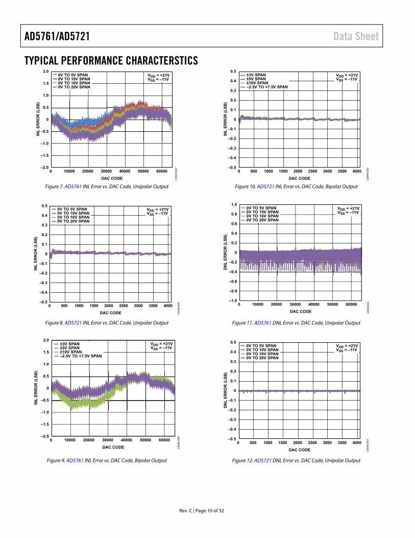
TYPICAL PERFORMANCE CHARACTERSTICS
–2.0
–1.5
–1.0
–0.5
0
0.5
1.0
1.5
2.0
0 10000 20000 30000 40000 50000 60000
DAC CODE
INL
ER
RO
R (
LS
B)
0V TO 5V SPAN0V TO 10V SPAN0V TO 16V SPAN0V TO 20V SPAN
VDD = +21VVSS = –11V
1264
0-00
7
Figure 7. AD5761 INL Error vs. DAC Code, Unipolar Output
–0.5
–0.4
–0.3
–0.2
–0.1
0
0.1
0.2
0.3
0.4
0.5
0 500 1000 1500 2000 2500 3000 3500 4000
DAC CODE
INL
ER
RO
R (
LS
B)
0V TO 5V SPAN0V TO 10V SPAN0V TO 16V SPAN0V TO 20V SPAN
VDD = +21VVSS = –11V
1264
0-00
8
Figure 8. AD5721 INL Error vs. DAC Code, Unipolar Output
–2.0
–1.5
–1.0
–0.5
0
0.5
1.0
1.5
2.0
0 10000 20000 30000 40000 50000 60000
DAC CODE
INL
ER
RO
R (
LS
B)
±3V SPAN±5V SPAN±10V SPAN–2.5V TO +7.5V SPAN
VDD = +21VVSS = –11V
1264
0-00
9
Figure 9. AD5761 INL Error vs. DAC Code, Bipolar Output
–0.5
–0.4
–0.3
–0.2
–0.1
0
0.1
0.2
0.3
0.4
0.5
0 500 1000 1500 2000 2500 3000 3500 4000
DAC CODE
INL
ER
RO
R (
LS
B)
VDD = +21VVSS = –11V
±3V SPAN±5V SPAN±10V SPAN–2.5V TO +7.5V SPAN
1264
0-01
0
Figure 10. AD5721 INL Error vs. DAC Code, Bipolar Output
–1.0
–0.8
–0.6
–0.4
–0.2
0
0.2
0.4
0.6
0.8
1.0
0 10000 20000 30000 40000 50000 60000
DAC CODE
DN
L E
RR
OR
(L
SB
)
VDD = +21VVSS = –11V
0V TO 5V SPAN0V TO 10V SPAN0V TO 16V SPAN0V TO 20V SPAN
1264
0-01
1
Figure 11. AD5761 DNL Error vs. DAC Code, Unipolar Output
–0.5
–0.4
–0.3
–0.2
–0.1
0
0.1
0.2
0.3
0.4
0.5
0 500 1000 1500 2000 2500 3000 3500 4000
DAC CODE
DN
L E
RR
OR
(L
SB
)
0V TO 5V SPAN0V TO 10V SPAN0V TO 16V SPAN0V TO 20V SPAN
VDD = +21VVSS = –11V
1264
0-01
2
Figure 12. AD5721 DNL Error vs. DAC Code, Unipolar Output

Data Sheet AD5761/AD5721
Rev. C | Page 11 of 32
–1.0
–0.8
–0.6
–0.4
–0.2
0
0.2
0.4
0.6
0.8
1.0
0 10000 20000 30000 40000 50000 60000
DAC CODE
DN
L E
RR
OR
(L
SB
)
VDD = +21VVSS = –11V
±3V SPAN±5V SPAN±10V SPAN–2.5V TO +7.5V SPAN
1264
0-01
3
Figure 13. AD5761 DNL Error vs. DAC Code, Bipolar Output
–0.5
–0.4
–0.3
–0.2
–0.1
0
0.1
0.2
0.3
0.4
0.5
0 500 1000 1500 2000 2500 3000 3500 4000
DAC CODE
DN
L E
RR
OR
(L
SB
)
VDD = +21VVSS = –11V
±3V SPAN±5V SPAN±10V SPAN–2.5V TO +7.5V SPAN
1264
0-01
4
Figure 14. AD5721 DNL Error vs. DAC Code, Bipolar Output
–2.0
–1.5
–1.0
–0.5
0
0.5
1.0
1.5
2.0
–40 –20 0 25 50 85 105 125
INL
ER
RO
R (
LS
B)
TEMPERATURE (°C)
VDD = +21VVSS = –11V
MAXIMUM INL, 0V TO 5V SPANMAXIMUM INL, ±10V SPANMINIMUM INL, 0V TO 5V SPANMINIMUM INL, ±10V SPAN
1264
0-01
5
Figure 15. INL Error vs. Temperature
–1.0
–0.8
–0.6
–0.4
–0.2
0
0.2
0.4
0.6
0.8
1.0
–40 –20 0 25 50 85 105 125
DN
L E
RR
OR
(L
SB
)
TEMPERATURE (°C)
VDD = +21VVSS = –11V
MAXIMUM DNL, 0V TO 5V SPANMAXIMUM DNL, ±10V SPANMINIMUM DNL, 0V TO 5V SPANMINIMUM DNL, ±10V SPAN
1264
0-01
6
Figure 16. DNL Error vs. Temperature
–2.0
–1.5
–1.0
–0.5
0
0.5
1.0
1.5
2.0
+5V SPAN AVDD/AVSS = +6V/–1V±10V SPAN AVDD/AVSS = +11V/–11V
AVDD/AVSS = +7.5V/–1VAVDD/AVSS = +12.5V/–12.5V
AVDD/AVSS = +10V/–1VAVDD/AVSS = +13.5V/–13.5V
AVDD/AVSS = +12.5V/–1VAVDD/AVSS = +14.5V/–14.5V
AVDD/AVSS = +16.5V/–1VAVDD/AVSS = +16.5V/–16.5V
SUPPLY VOLTAGE (V)
INL
ER
RO
R (
LS
B)
VDD = +21VVSS = –11VTA = 25°CNO LOAD
1264
0-01
7
MAXIMUM INL, 0V TO 5V SPANMAXIMUM INL, ±10V SPANMINIMUM INL, 0V TO 5V SPANMINIMUM INL, ±10V SPAN
Figure 17. INL Error vs. Supply Voltage
+5V SPAN AVDD/AVSS = +6V/–1V±10V SPAN AVDD/AVSS = +11V/–11V
AVDD/AVSS = +7.5V/–1VAVDD/AVSS = +12.5V/–12.5V
AVDD/AVSS = +10V/–1VAVDD/AVSS = +13.5V/–13.5V
AVDD/AVSS = +12.5V/–1VAVDD/AVSS = +14.5V/–14.5V
AVDD/AVSS = +16.5V/–1VAVDD/AVSS = +16.5V/–16.5V
–1.0
–0.8
–0.6
–0.4
–0.2
0
0.2
0.4
0.6
0.8
1.0
SUPPLY VOLTAGE (V)
DN
L E
RR
OR
(L
SB
)
VDD = +21VVSS = –11VTA = 25°CNO LOAD
1264
0-01
8
MAXIMUM DNL, 0V TO 5V SPANMAXIMUM DNL, ±10V SPANMINIMUM DNL, 0V TO 5V SPANMINIMUM DNL, ±10V SPAN
Figure 18. DNL Error vs. Supply Voltage
AD5761/AD5721 Data Sheet
Rev. C | Page 12 of 31
–3
–2
–1
0
1
2
3
2.00 2.25 2.50 2.75 3.00
INL
ERRO
R (L
SB)
REFERENCE VOLTAGE (V)
VDD = +21VVSS = –11V
MAXIMUM INL, 0V TO 5V SPANMAXIMUM INL, ±10V SPANMINIMUM INL, 0V TO 5V SPANMINIMUM INL, ±10V SPAN
1264
0-01
9
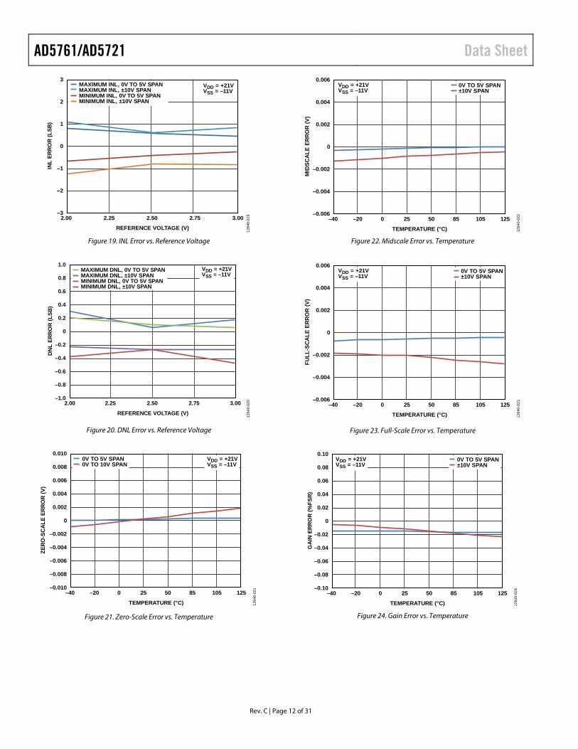
Figure 19. INL Error vs. Reference Voltage
–1.0
–0.8
–0.6
–0.4
–0.2
0
0.2
0.4
0.6
0.8
1.0
DN
L ER
RO
R (L
SB)
MAXIMUM DNL, 0V TO 5V SPANMAXIMUM DNL, ±10V SPANMINIMUM DNL, 0V TO 5V SPANMINIMUM DNL, ±10V SPAN
REFERENCE VOLTAGE (V)
VDD = +21VVSS = –11V
1264
0-02
02.00 2.25 2.50 2.75 3.00
Figure 20. DNL Error vs. Reference Voltage
–40 –20 0 25 50 85 105 125
TEMPERATURE (°C)
–0.010
–0.008
–0.006
–0.004
–0.002
0
0.002
0.004
0.006
0.008
0.010
ZERO
-SCA
LE E
RRO
R (V
)
0V TO 5V SPAN0V TO 10V SPAN
VDD = +21VVSS = –11V
1264
0-02
1
Figure 21. Zero-Scale Error vs. Temperature
–0.006
–0.004
–0.002
0
0.002
0.004
0.006
–40 –20 0 25 50 85 105 125
TEMPERATURE (°C)
MID
SCAL
E ER
ROR
(V)
VDD = +21VVSS = –11V
0V TO 5V SPAN±10V SPAN
1264
0-02
2
Figure 22. Midscale Error vs. Temperature
–0.006
–0.004
–0.002
0
0.002
0.004
0.006
–40 –20 0 25 50 85 105 125
TEMPERATURE (°C)
FULL
-SCA
LE E
RRO
R (V
)
VDD = +21VVSS = –11V
0V TO 5V SPAN±10V SPAN
1264
0-02
3
Figure 23. Full-Scale Error vs. Temperature
–40 –20 0 25 50 85 105 125
TEMPERATURE (°C)
–0.10
–0.08
–0.06
–0.04
–0.02
0
0.02
0.04
0.06
0.08
0.10
GAI
N ER
ROR
(%FS
R)
VDD = +21VVSS = –11V
0V TO 5V SPAN±10V SPAN
1264
0-02
4
Figure 24. Gain Error vs. Temperature
Data Sheet AD5761/AD5721
Rev. C | Page 13 of 32
–0.0030
–0.0025
–0.0020
–0.0015
–0.0010
–0.0005
0
0.0005
0.00100V TO 5V SPAN±10V SPAN
SUPPLY VOLTAGE (V)
ZE
RO
-SC
AL
E E
RR
OR
(V
)
TA = 25°CVREF = 2.5V
+5V SPAN AVDD/AVSS = +6V/–1V±10V SPAN AVDD/AVSS = +11V/–11V
AVDD/AVSS = +7.5V/–1VAVDD/AVSS = +12.5V/–12.5V
AVDD/AVSS = +10V/–1VAVDD/AVSS = +13.5V/–13.5V
AVDD/AVSS = +12.5V/–1VAVDD/AVSS = +14.5V/–14.5V
AVDD/AVSS = +16.5V/–1VAVDD/AVSS = +16.5V/–16.5V
1264
0-02
5
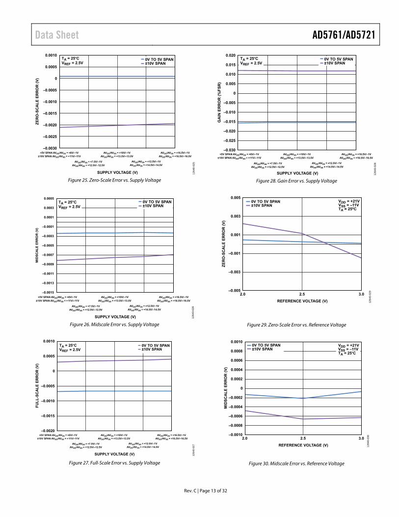
Figure 25. Zero-Scale Error vs. Supply Voltage
–0.0015
–0.0013
–0.0011
–0.0009
–0.0007
–0.0005
–0.0003
–0.0001
0.0001
0.0003
0.00050V TO 5V SPAN±10V SPAN
MID
SC
AL
E E
RR
OR
(V
)
TA = 25°CVREF = 2.5V
1264
0-02
6
SUPPLY VOLTAGE (V)
+5V SPAN AVDD/AVSS = +6V/–1V±10V SPAN AVDD/AVSS = +11V/–11V
AVDD/AVSS = +7.5V/–1VAVDD/AVSS = +12.5V/–12.5V
AVDD/AVSS = +10V/–1VAVDD/AVSS = +13.5V/–13.5V
AVDD/AVSS = +12.5V/–1VAVDD/AVSS = +14.5V/–14.5V
AVDD/AVSS = +16.5V/–1VAVDD/AVSS = +16.5V/–16.5V
Figure 26. Midscale Error vs. Supply Voltage
SUPPLY VOLTAGE (V)
–0.0020
–0.0015
–0.0010
–0.0005
0
0.0005
0.0010
+5V SPAN AVDD/AVSS = +6V/–1V±10V SPAN AVDD/AVSS = +11V/–11V
AVDD/AVSS = +7.5V/–1VAVDD/AVSS = +12.5V/–12.5V
AVDD/AVSS = +10V/–1VAVDD/AVSS = +13.5V/–13.5V
AVDD/AVSS = +12.5V/–1VAVDD/AVSS = +14.5V/–14.5V
AVDD/AVSS = +16.5V/–1VAVDD/AVSS = +16.5V/–16.5V
FU
LL
-SC
AL
E E
RR
OR
(V
)
TA = 25°CVREF = 2.5V
1264
0-02
7
0V TO 5V SPAN±10V SPAN
Figure 27. Full-Scale Error vs. Supply Voltage
–0.030
–0.025
–0.020
–0.015
–0.010
–0.005
0
0.005
0.010
0.015
0.020
GA
IN E
RR
OR
(%
FS
R)
0V TO 5V SPAN±10V SPAN
TA = 25°CVREF = 2.5V
SUPPLY VOLTAGE (V)
+5V SPAN AVDD/AVSS = +6V/–1V±10V SPAN AVDD/AVSS = +11V/–11V
AVDD/AVSS = +7.5V/–1VAVDD/AVSS = +12.5V/–12.5V
AVDD/AVSS = +10V/–1VAVDD/AVSS = +13.5V/–13.5V
AVDD/AVSS = +12.5V/–1VAVDD/AVSS = +14.5V/–14.5V
AVDD/AVSS = +16.5V/–1VAVDD/AVSS = +16.5V/–16.5V
1264
0-02
8
Figure 28. Gain Error vs. Supply Voltage
–0.005
–0.003
–0.001
0.001
0.003
0.005
2.0 2.5 3.0
0V TO 5V SPAN±10V SPAN
REFERENCE VOLTAGE (V)
ZE
RO
-SC
AL
E E
RR
OR
(V
)
VDD = +21VVSS = –11VTA = 25⁰C
1264
0-02
9
Figure 29. Zero-Scale Error vs. Reference Voltage
–0.0010
–0.0008
–0.0006
–0.0004
–0.0002
0
0.0002
0.0004
0.0006
0.0008
0.0010
2.0 2.5 3.0
REFERENCE VOLTAGE (V)
MID
SC
AL
E E
RR
OR
(V
)
0V TO 5V SPAN±10V SPAN
VDD = +21VVSS = –11VTA = 25°C
1264
0-03
0
Figure 30. Midscale Error vs. Reference Voltage

AD5761/AD5721 Data Sheet
Rev. C | Page 14 of 31
–0.005
–0.003
–0.001
0.001
0.003
0.005
2.0 2.5 3.0
REFERENCE VOLTAGE (V)
FULL
-SC
ALE
ER
RO
R (V
)
0V TO 5V SPAN±10V SPAN
VDD = +21VVSS = –11VTA = 25°C
1264
0-03
1
Figure 31. Full-Scale Error vs. Reference Voltage
–0.05
–0.03
–0.01
0.01
0.03
0.05
2.0 2.5 3.0
0V TO 5V SPAN±10V SPAN
REFERENCE VOLTAGE (V)
GA
IN E
RR
OR
(%FS
R)
VDD = +21VVSS = –11VTA = 25°C
1264
0-03
2
Figure 32. Gain Error vs. Reference Voltage
–0.05
–0.03
–0.01
0.01
0.03
0.05
0 10000 20000 30000 40000 50000 60000
0V TO 5V SPAN0V TO 10V SPAN0V TO 16V SPAN0V TO 20V SPAN
TUE
(%FS
R)
CODE 1264
0-03
3
TA = 25°C
Figure 33. TUE vs. Code, Unipolar Output
TUE
(%FS
R)
–0.05
–0.03
–0.01
0.01
0.03
0.05
0 10000 20000 30000 40000 50000 60000
±5V SPAN±10V SPAN–2.5V TO +7.5V SPAN±3V SPAN
CODE 1264
0-03
4
TA = 25°C
Figure 34. TUE vs. Code, Bipolar Output
0
0.005
0.010
0.015
0.020
0.025
0.0300V TO 5V SPAN±10V SPAN
TEMPERATURE (°C)
TUE
(%FS
R)
VDD = +21VVSS = –11V
1264
0-13
5
–40 –20 0 25 50 85 105 125
Figure 35. TUE vs. Temperature
0
0.002
0.004
0.006
0.008
0.010
0.012
0.014
0.016
0.018
0.020
TUE
(%FS
R)
0V TO 5V SPAN±10V SPAN
TA = 25°CVREF = 2.5V
SUPPLY VOLTAGE (V)
+5V SPAN AVDD/AVSS = +6V/–1V±10V SPAN AVDD/AVSS = +11V/–11V
AVDD/AVSS = +7.5V/–1VAVDD/AVSS = +12.5V/–12.5V
AVDD/AVSS = +10V/–1VAVDD/AVSS = +13.5V/–13.5V
AVDD/AVSS = +12.5V/–1VAVDD/AVSS = +14.5V/–14.5V
AVDD/AVSS = +16.5V/–1VAVDD/AVSS = +16.5V/–16.5V
1264
0-03
6
Figure 36. TUE vs. Supply Voltage
Data Sheet AD5761/AD5721
Rev. C | Page 15 of 31
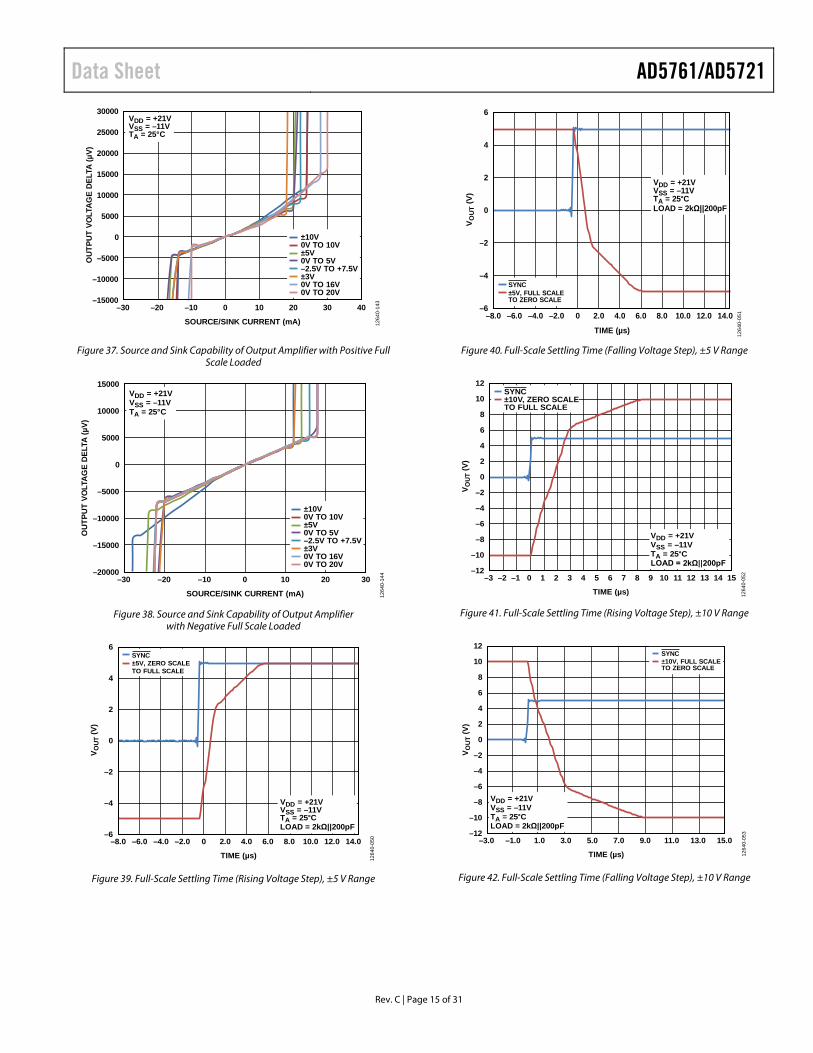
–15000
–10000
–5000
0
5000
10000
15000
20000
25000
30000
–30 –20 –10 0 10 20 30 40
VDD = +21VVSS = –11VTA = 25°C
±10V0V TO 10V±5V0V TO 5V–2.5V TO +7.5V±3V0V TO 16V0V TO 20V
SOURCE/SINK CURRENT (mA)
OU
TPU
T VO
LTA
GE
DEL
TA (µ
V)
1264
0-14
3
Figure 37. Source and Sink Capability of Output Amplifier with Positive Full Scale Loaded
–20000
–15000
–10000
–5000
0
5000
10000
15000
–30 –20 –10 0 10 20 30
SOURCE/SINK CURRENT (mA)
OUT
PUT
VOLT
AGE
DELT
A (µ
V)
VDD = +21VVSS = –11VTA = 25°C
±10V0V TO 10V±5V0V TO 5V–2.5V TO +7.5V±3V0V TO 16V0V TO 20V
1264
0-14
4
Figure 38. Source and Sink Capability of Output Amplifier with Negative Full Scale Loaded
1264
0-05
0–6
–4
–2
0
2
4
6
–8.0 –6.0 –4.0 –2.0 0 2.0 4.0 6.0 8.0 10.0 12.0 14.0
V OUT
(V)
TIME (µs)
SYNC±5V, ZERO SCALETO FULL SCALE
VDD = +21VVSS = –11VTA = 25°CLOAD = 2kΩ||200pF
Figure 39. Full-Scale Settling Time (Rising Voltage Step), ±5 V Range
1264
0-05
1–6
–4
–2
0
2
4
6
–8.0 –6.0 –4.0 –2.0 0 2.0 4.0 6.0 8.0 10.0 12.0 14.0
V OU
T (V
)
TIME (µs)
VDD = +21VVSS = –11VTA = 25°CLOAD = 2kΩ||200pF
SYNC±5V, FULL SCALETO ZERO SCALE
Figure 40. Full-Scale Settling Time (Falling Voltage Step), ±5 V Range
1264
0-05
2–12
–10
–8
–6
–4
–2
0
2
4
6
8
10
12
–3 –2 –1 0 1 2 3 4 5 6 7 8 9 10 11 12 13 14 15
TIME (µs)
V OUT
(V)
VDD = +21VVSS = –11VTA = 25°CLOAD = 2kΩ||200pF
SYNC±10V, ZERO SCALETO FULL SCALE
Figure 41. Full-Scale Settling Time (Rising Voltage Step), ±10 V Range
1264
0-05
3–12
–10
–8
–6
–4
–2
0
2
4
6
8
10
12
–3.0 –1.0 1.0 3.0 5.0 7.0 9.0 11.0 13.0 15.0
TIME (µs)
VDD = +21VVSS = –11VTA = 25°CLOAD = 2kΩ||200pF
V OUT
(V)
SYNC±10V, FULL SCALETO ZERO SCALE
Figure 42. Full-Scale Settling Time (Falling Voltage Step), ±10 V Range
AD5761/AD5721 Data Sheet
Rev. C | Page 16 of 31
–0.01
0
0.01
0.02
0.03
0.04
0.05
0.06
0.07
0.08
0.09
0.10
–2 –1 0 1 2 3 4 5
V OUT
(V)
TIME (µs)
SYNC500-CODE STEP, ±5V SPAN
VDD = +21VVSS = –11VTA = 25°CLOAD = 2kΩ||200pF
1264
0-15
0
Figure 43. 500-Code Step Settling Time, ±5 V Range
–2 –1 0 1 2 3 4 5
V OUT
(V)
TIME (µs) 1264
0-15
1–0.010
0.010.020.030.040.050.060.070.080.090.100.110.120.130.140.150.160.170.180.190.20
VDD = +21VVSS = –11VTA = 25°CLOAD = 2kΩ||200pF
SYNC500-CODE STEP, ±10V SPAN
Figure 44. 500-Code Step Settling Time, ±10 V Range
–12
–10
–8
–6
–4
–2
0
2
4
6
8
10
12
–5 0 5 10 15 20
TIME (µs)
0nF1nF5nF7nF10nF
V OUT
(V)
VDD =+21VVSS = –11VTA = 25°CLOAD = 2kΩ
1264
0-05
6
Figure 45. Settling Time vs. Capacitive Load, ±10 V Range
0
0.5
1.0
1.5
2.0
2.5
3.0
3.5
4.0
4.5
5.0
5.5
6.0
–3 –2 –1 10 2 3 4 5 6 7 8 9 10 11 12 13 14 15TIME (µs)
0nF1nF5nF7nF10nF
V OU
T (V
)
VDD = +21VVSS = –11VTA = 25°CLOAD = 2kΩ
1264
0-05
7
Figure 46. Settling Time vs. Capacitive Load, 0 V to 5 V Range
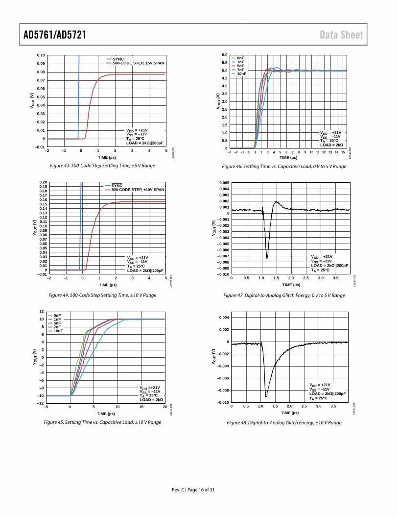
–0.010–0.009–0.008–0.007–0.006–0.005–0.004–0.003–0.002–0.001
00.0010.0020.0030.0040.005
0 0.5 1.0 1.5 2.0 2.5 3.0 3.5
V OUT
(V)
TIME (µs)
VDD = +21VVSS = –11VLOAD = 2kΩ||200pFTA = 25°C
1264
0-35
4
Figure 47. Digital-to-Analog Glitch Energy, 0 V to 5 V Range
0 0.5 1.0 1.5 2.0 2.5 3.0 3.5
V OUT
(V)
TIME (µs)
–0.010
–0.008
–0.006
–0.004
–0.002
0
0.002
0.004
VDD = +21VVSS = –11VLOAD = 2kΩ||200pFTA = 25°C
1264
0-35
5
Figure 48. Digital-to-Analog Glitch Energy, ±10 V Range
Data Sheet AD5761/AD5721
Rev. C | Page 17 of 31
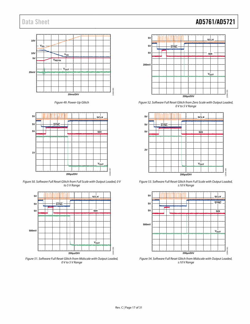
2
20ms/DIV
10V
5V
20mV
10V
VDD
VOUT
VSS
VREFIN
1264
0-06
0
Figure 49. Power-Up Glitch
1264
0-35
7
200µs/DIV
5V
5V
1V
5V
SCLK
SYNC
SDI
VOUT
Figure 50. Software Full Reset Glitch from Full Scale with Output Loaded, 0 V to 5 V Range
1264
0-35
8
SCLK
200µs/DIV
5V
5V
500mV
5V SYNC
SDI
VOUT
Figure 51. Software Full Reset Glitch from Midscale with Output Loaded,
0 V to 5 V Range
1264
0-35
9
SCLK
SYNC
SDI
VOUT
200µs/DIV
5V
5V
200mV
5V
Figure 52. Software Full Reset Glitch from Zero Scale with Output Loaded, 0 V to 5 V Range
1264
0-36
0
SCLK
200µs/DIV
5V
5V
2V
5V SYNC
SDI
VOUT
Figure 53. Software Full Reset Glitch from Full Scale with Output Loaded, ±10 V Range
1264
0-36
1
SCLK
200µs/DIV
5V
5V
500mV
5V SYNC
SDI
VOUT
Figure 54. Software Full Reset Glitch from Midscale with Output Loaded,
±10 V Range

AD5761/AD5721 Data Sheet
Rev. C | Page 18 of 32
1264
0-36
2
SCLK
SDI
200µs/DIV
5V
5V
2V
5V SYNC
VOUT
Figure 55. Software Full Reset Glitch from Zero Scale with Output Loaded, ±10 V Range
1264
0-05
8
200µs/DIV
5V
5V
1V
5V
SCLK
SYNC
SDI
VOUT
Figure 56. Output Range Change Glitch, 0 V to 5 V Range
1264
0-05
9
200µs/DIV
5V
5V
200mV
5V
SCLK
SYNC
SDI
VOUT
Figure 57. Output Range Change Glitch, ±10 V Range
–4
–2
0
2
4
6
8
10
–2.0 –1.5 –1.0 –0.5 0 0.5 1.0 1.5 2.0
NO
ISE
(µ
V p
-p)
TIME (Seconds)
VDD = +21VVSS = –11VVREFIN = 2.5VTA = 25°C
1264
0-16
1
Figure 58. Peak-to-Peak Noise (Voltage Output Noise), 0.1 Hz to 10 Hz Bandwidth
–30
–20
–10
0
10
20
30
–2.0 2.0–1.5 –1.0 –0.5 0 0.5 1.0 1.5
NO
ISE
(µ
V R
MS
)
TIME (Seconds) 1264
0-13
9
VDD = +21VVSS = –11VTA = 25°C
Figure 59. Peak-to-Peak Noise (Voltage Output Noise), 100 kHz Bandwidth
NS
D (
nV
/√H
z)
FREQUENCY (Hz)
DAC OUTPUT NSD (nV/√Hz), EXT REF, ZSDAC OUTPUT NSD (nV/√Hz), EXT REF, MSDAC OUTPUT NSD (nV/√Hz), EXT REF, FS
VDD = +21VVSS = –11VTA = 25°C
1264
0-16
3
Figure 60. DAC Output Noise Spectral Density vs. Frequency, ±10 V Range

Data Sheet AD5761/AD5721
Rev. C | Page 19 of 32
–160
–140
–120
–100
–80
–60
–40
–20
0
TH
D (
dB
V)
FREQUENCY (kHz)
0 2 4 6 8 10 12 14 16 18 20
1264
0-46
0
Figure 61. Total Harmonic Distortion at 1 kHz
–0.0010
–0.0005
0
0.0005
0.0010
0.0015
24.1
24.1
24.2
24.3
24.4
24.5
24.5
24.6
24.7
24.8
24.9
24.9
25.0
25.1
25.2
25.3
25.3
25.4
25.5
25.6
25.7
25.7
25.8
25.9
DIG
ITA
L F
EE
DT
HR
OU
GH
(V
p-p
)
TIME (µs)
TA = 25°CAVDD = +21VAVSS = –11VDVCC = 5V2.5V EXT REFLOAD = 2kΩ||200pF
1264
0-16
5
Figure 62. Digital Feedthrough
AD5761/AD5721 Data Sheet
Rev. C | Page 20 of 31
TERMINOLOGY Total Unadjusted Error (TUE) Total unadjusted error is a measure of the output error taking all the various errors into account, namely INL error, offset error, gain error, and output drift over supplies, temperature, and time. TUE is expressed in % FSR.
Relative Accuracy or Integral Nonlinearity (INL) For the DAC, relative accuracy, or integral nonlinearity, is a measure of the maximum deviation, in LSB, from a straight line passing through the endpoints of the DAC transfer function. A typical INL error vs. DAC code plot is shown in Figure 7.
Differential Nonlinearity (DNL) Differential nonlinearity is the difference between the measured change and the ideal 1 LSB change between any two adjacent codes. A specified differential nonlinearity of ±1 LSB maximum ensures monotonicity. This DAC is guaranteed monotonic. A typical DNL error vs. code plot is shown in Figure 11.
Monotonicity A DAC is monotonic if the output either increases or remains constant for increasing digital input code. The AD5761/AD5721 are monotonic over their full operating temperature range.
Bipolar Zero Error Bipolar zero error is the deviation of the analog output from the ideal half-scale output of 0 V when the DAC register is loaded with 0x8000 (straight binary coding) or 0x0000 (twos complement coding) for the AD5761/AD5721.
Bipolar Zero Temperature Coefficient (TC) Bipolar zero TC is a measure of the change in the bipolar zero error with a change in temperature. It is expressed in µV/°C.
Zero-Scale Error Zero-scale error is the error in the DAC output voltage when 0x0000 (straight binary coding) or 0x8000 (twos complement coding) is loaded to the DAC register. Ideally, the output voltage is negative full scale. A plot of zero-scale error vs. temperature is shown in Figure 21.
Zero-Scale Error Temperature Coefficient (TC) Zero-scale error TC is a measure of the change in zero-scale error with a change in temperature. It is expressed in µV/°C.
Offset Error Offset error is a measure of the difference between VOUT (actual) and VOUT (ideal) expressed in mV in the linear region of the transfer function.
Offset Error Temperature Coefficient (TC) Offset error TC is a measurement of the change in offset error with a change in temperature. It is expressed in µV/°C.
Gain Error Gain error is a measure of the span error of the DAC. It is the deviation in slope of the DAC transfer characteristic from the ideal expressed in % FSR. A plot of gain error vs. temperature is shown in Figure 24.
Gain Error Temperature Coefficient (TC) Gain error TC is a measure of the change in gain error with changes in temperature. It is expressed in ppm FSR/°C.
DC Power Supply Rejection Ratio (DC PSRR) DC power supply rejection ratio is a measure of the rejection of the output voltage to dc changes in the power supplies applied to the DAC. It is measured for a given dc change in power supply voltage and is expressed in mV/V.
AC Power Supply Rejection Ratio (AC PSRR) AC power supply rejection ratio is a measure of the rejection of the output voltage to ac changes in the power supplies applied to the DAC. It is measured for a given amplitude and frequency change in power supply voltage and is expressed in decibels.
Output Voltage Settling Time Output voltage settling time is the amount of time it takes for the output to settle to a specified level for a full-scale input change. Full-scale settling time is shown in Figure 39 to Figure 42.
Digital-to-Analog Glitch Impulse Digital-to-analog glitch impulse is the impulse injected into the analog output when the input code in the DAC register changes state. It is normally specified as the area of the glitch in nV-sec and is measured when the digital input code is changed by 1 LSB at the major carry transition (see Figure 47 and Figure 48).
Glitch Impulse Peak Amplitude Glitch impulse peak amplitude is the peak amplitude of the impulse injected into the analog output when the input code in the DAC register changes state. It is specified as the amplitude of the glitch in mV and is measured when the digital input code is changed by 1 LSB at the major carry transition.
Digital Feedthrough Digital feedthrough is a measure of the impulse injected into the analog output of the DAC from the digital inputs of the DAC but is measured when the DAC output is not updated. It is specified in nV-sec and measured with a full-scale code change on the data bus.
Noise Spectral Density Noise spectral density is a measurement of the internally generated random noise characterized as a spectral density (nV/√Hz). It is measured by loading the DAC to full scale and measuring noise at the output. It is measured in nV/√Hz. A plot of noise spectral density is shown in Figure 60.
Total Harmonic Distortion (THD) THD is the ratio of the rms sum of harmonics to the fundamental.
For the AD5761/AD5721, it is defined as
1
26
25
24
23
22log20)dB(
VVVVVV
THD++++
×=
where:
V1 is the rms amplitude of the fundamental. V2, V3, V4, V5, and V6 are the rms amplitudes of the second through the sixth harmonics.
Data Sheet AD5761/AD5721
Rev. C | Page 21 of 31
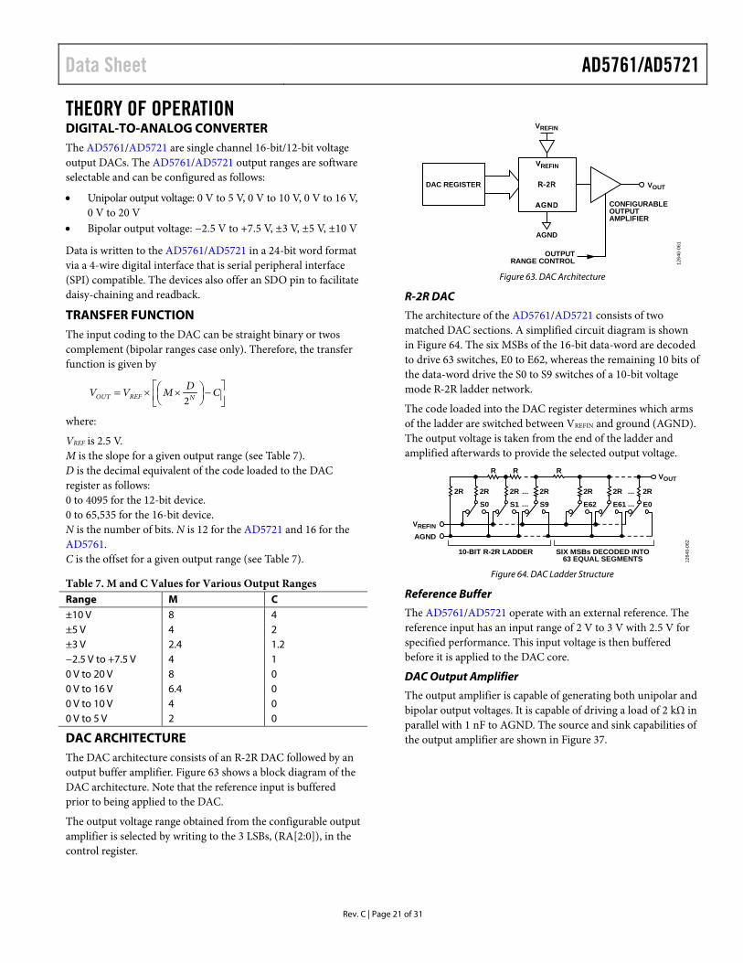
THEORY OF OPERATION DIGITAL-TO-ANALOG CONVERTER The AD5761/AD5721 are single channel 16-bit/12-bit voltage output DACs. The AD5761/AD5721 output ranges are software selectable and can be configured as follows:
• Unipolar output voltage: 0 V to 5 V, 0 V to 10 V, 0 V to 16 V, 0 V to 20 V
• Bipolar output voltage: −2.5 V to +7.5 V, ±3 V, ±5 V, ±10 V
Data is written to the AD5761/AD5721 in a 24-bit word format via a 4-wire digital interface that is serial peripheral interface (SPI) compatible. The devices also offer an SDO pin to facilitate daisy-chaining and readback.
TRANSFER FUNCTION The input coding to the DAC can be straight binary or twos complement (bipolar ranges case only). Therefore, the transfer function is given by
−
××= CDMVV NREFOUT 2
where:
VREF is 2.5 V. M is the slope for a given output range (see Table 7). D is the decimal equivalent of the code loaded to the DAC register as follows: 0 to 4095 for the 12-bit device. 0 to 65,535 for the 16-bit device. N is the number of bits. N is 12 for the AD5721 and 16 for the AD5761. C is the offset for a given output range (see Table 7).
Table 7. M and C Values for Various Output Ranges Range M C ±10 V 8 4 ±5 V 4 2 ±3 V 2.4 1.2 −2.5 V to +7.5 V 4 1 0 V to 20 V 8 0 0 V to 16 V 6.4 0 0 V to 10 V 4 0 0 V to 5 V 2 0
DAC ARCHITECTURE The DAC architecture consists of an R-2R DAC followed by an output buffer amplifier. Figure 63 shows a block diagram of the DAC architecture. Note that the reference input is buffered prior to being applied to the DAC.
The output voltage range obtained from the configurable output amplifier is selected by writing to the 3 LSBs, (RA[2:0]), in the control register.
AGND
REFIN
CONFIGURABLEOUTPUTAMPLIFIER
OUTPUTRANGE CONTROL
VREFIN
DAC REGISTER VOUT
1264
0-06
1
Figure 63. DAC Architecture
R-2R DAC
The architecture of the AD5761/AD5721 consists of two matched DAC sections. A simplified circuit diagram is shown in Figure 64. The six MSBs of the 16-bit data-word are decoded to drive 63 switches, E0 to E62, whereas the remaining 10 bits of the data-word drive the S0 to S9 switches of a 10-bit voltage mode R-2R ladder network.
The code loaded into the DAC register determines which arms of the ladder are switched between VREFIN and ground (AGND). The output voltage is taken from the end of the ladder and amplified afterwards to provide the selected output voltage.
2R
S0
2R 2R
10-BIT R-2R LADDER SIX MSBs DECODED INTO63 EQUAL SEGMENTS
S1
2R
S9
2R
RRR
E62
2R ...
...
...
... E61
2R
VOUT
VREFIN
AGND
E0
1264
0-06
2
Figure 64. DAC Ladder Structure
Reference Buffer
The AD5761/AD5721 operate with an external reference. The reference input has an input range of 2 V to 3 V with 2.5 V for specified performance. This input voltage is then buffered before it is applied to the DAC core.
DAC Output Amplifier
The output amplifier is capable of generating both unipolar and bipolar output voltages. It is capable of driving a load of 2 kΩ in parallel with 1 nF to AGND. The source and sink capabilities of the output amplifier are shown in Figure 37.

AD5761/AD5721 Data Sheet
Rev. C | Page 22 of 31
SERIAL INTERFACE
The AD5761/AD5721 4-wire (SYNC, SCLK, SDI, and SDO) digital interface is SPI compatible. The write sequence begins after bringing the SYNC line low, maintaining this line low until the complete data-word is loaded from the SDI pin. Data is loaded in at the SCLK falling edge transition (see Figure 2). When SYNC is brought high again, the serial data-word is decoded according to the instructions in Table 10. The AD5761/AD5721 contain an SDO pin to allow the user to daisy-chain multiple devices together or to read back the contents of the registers.
Standalone Operation
The serial interface works with both a continuous and noncontinu-ous serial clock. A continuous SCLK source can be used only when SYNC is held low for the correct number of clock cycles.
In gated clock mode, a burst clock containing the exact number of clock cycles must be used, and SYNC must be taken high after the final clock to latch the data. The first falling edge of SYNC starts the write cycle. Exactly 24 falling clock edges must be applied to SCLK before SYNC is brought high again. If SYNC is brought high before the 24th falling SCLK edge, the data written is invalid. If more than 24 falling SCLK edges are applied before SYNC is brought high, the input data is also invalid.
The input shift register is updated on the rising edge of SYNC. For another serial transfer to take place, SYNC must be brought low again. After the end of the serial data transfer, data is automatically transferred from the input shift register to the addressed register. When the write cycle is complete, the output can be updated by taking LDAC low while SYNC is high.
Readback Operation
The contents of the input, DAC, and control registers can be read back via the SDO pin. Figure 4 shows how the registers are decoded. After a register has been addressed for a read, the next 24 clock cycles clock the data out on the SDO pin. The clocks must be applied while SYNC is low. When SYNC is returned high, the SDO pin is placed in tristate. For a read of a single register, the no operation (NOP) function clocks out the data. Alternatively, if more than one register is to be read, the data of the first register to be addressed clocks out at the same time that the second register to be read is being addressed. The SDO pin must be enabled to complete a readback operation. The SDO pin is enabled by default.
Daisy-Chain Operation
For systems that contain several devices, use the SDO pin to daisy-chain several devices together. Daisy-chain mode is useful in system diagnostics and in reducing the number of serial interface lines. The first falling edge of SYNC starts the write cycle. SCLK is continuously applied to the input shift register when SYNC is low. If more than 24 clock pulses are applied, the data ripples out of the shift register and appears on the SDO line. This data is clocked out on the rising edge of SCLK and is valid on the falling edge.
By connecting the SDO of the first device to the SDI input of the next device in the chain, a multidevice interface is constructed. Each device in the system requires 24 clock pulses. Therefore, the total number of clock cycles must equal 24 × N, where N is the total number of AD5761/AD5721 devices in the chain. When the serial transfer to all devices is complete, SYNC is taken high, which latches the input data in each device in the daisy chain and prevents any further data from being clocked into the input shift register.
*ADDITIONAL PINS OMITTED FOR CLARITY.
CONTROLLER
DATA IN
SDI
SCLK
DATA OUT
SERIAL CLOCK
CONTROL OUT
SDO
SCLK
SDO
SCLK
SDO
SDI
SDI
SYNC
SYNC
SYNC
AD5761/AD5721*
AD5761/AD5721*
AD5761/AD5721*
1264
0-06
3
Figure 65. Daisy-Chain Block Diagram
HARDWARE CONTROL PINS Load DAC Function (LDAC)
After data transfers into the input register of the DAC, there are two ways to update the DAC register and DAC output. Depend-ing on the status of both SYNC and LDAC, one of two update modes is selected: synchronous DAC update or asynchronous DAC update.
Synchronous DAC Update
In synchronous DAC update mode, LDAC is held low while data is being clocked into the input shift register. The DAC output is updated on the rising edge of SYNC.
Data Sheet AD5761/AD5721
Rev. C | Page 23 of 31
Asynchronous DAC Update
In asynchronous DAC update mode, LDAC is held high while data is being clocked into the input shift register. The DAC output is asynchronously updated by taking LDAC low after SYNC is taken high. The update then occurs on the falling edge of LDAC.
Reset Function (RESET)
The AD5761/AD5721 can be reset to its power-on state by two means: either by asserting the RESET pin or by using the software full reset registers (see Table 26).
Asynchronous Clear Function (CLEAR)
The CLEAR pin is a falling edge active input that allows the output to be cleared to a user defined value. The clear code value is programmed by writing to Bit 10 and Bit 9 in the control register (see Table 11 and Table 12). It is necessary to maintain CLEAR low for a minimum amount of time to complete the operation (see Figure 2). When the CLEAR signal is returned high, the output remains at the clear value until a new value is loaded to the DAC register.
Alert Function (ALERT)
When the ALERT pin is asserted low, a readback from the control register is required to clarify whether a short-circuit or brownout condition occurred, depending on the values of Bit 12 and Bit 11, SC and BO bits, respectively (see Table 15 and Table 16). If neither of these conditions occurred, the temperature exceeded approximately 150°C.
The ALERT pin is low during power-up, a software full reset, or a hardware reset. After the first write to the control register to configure the DAC, the ALERT pin is asserted high.
In the event of the die temperature exceeding approximately 150°C, the ALERT pin is low and the value of the ETS bit determines the state of the digital supply of the device, whether the internal digital supply is powered on or powered down. If the ETS bit is set to 0, the internal digital supply is powered on when the internal die temperature exceeds approximately 150°C. If the ETS bit is set to 1, the internal digital supply is powered down when the internal die temperature exceeds approximately 150°C and the device becomes nonfunctional (see Table 11 and Table 12).
The AD5761/AD5721 temperature at power-up must be less than 150°C for proper operation of the devices.

AD5761/AD5721 Data Sheet
Rev. C | Page 24 of 31
REGISTER DETAILS INPUT SHIFT REGISTER The input shift register is 24 bits wide. Data is loaded into the device MSB first as a 24-bit word under the control of a serial clock input, SCLK, which can operate at rates of up to 50 MHz. The input shift register consists of three don’t care bits, one fixed value bit (DB20 = 0), four address bits, and a 16-bit or 12-bit data-word as shown in Table 8 and Table 9, respectively.
Table 8. AD5761 16-Bit Input Shift Register Format MSB LSB DB23 DB22 DB21 DB20 DB19 DB18 DB17 DB16 DB15 to DB0 X1 X1 X1 0 Register address Register data 1 X means don’t care.
Table 9. AD5721 12-Bit Input Shift Register Format MSB LSB DB23 DB22 DB21 DB20 DB19 DB18 DB17 DB16 DB15 to DB4 DB3 to DB0 X1 X1 X1 0 Register address Register data XXXX1 1 X means don’t care.
Table 10. Input Shift Register Commands Register Address
DB19 DB18 DB17 DB16 Command 0 0 0 0 No operation 0 0 0 1 Write to input register (no update) 0 0 1 0 Update DAC register from input register 0 0 1 1 Write and update DAC register 0 1 0 0 Write to control register 0 1 0 1 No operation 0 1 1 0 No operation 0 1 1 1 Software data reset 1 0 0 0 Reserved 1 0 0 1 Disable daisy-chain functionality 1 0 1 0 Readback input register 1 0 1 1 Readback DAC register 1 1 0 0 Readback control register 1 1 0 1 No operation 1 1 1 0 No operation 1 1 1 1 Software full reset
CONTROL REGISTER The control register controls the mode of operation of the AD5761/AD5721. The control register options are shown in Table 11 and Table 12.
On power-up, after a full reset, or after a hardware reset, the output of the DAC is clamped to ground through a 1 kΩ resistor and the output buffer remains in power-down mode. A write to the control register is required to configure the device, remove the clamp to ground, and power up the output buffer.
When the DAC output range is reconfigured during operation, a software full reset command (see Table 26) must be written to the device before writing to the control register.
Table 11. Write to Control Register MSB LSB DB[23:21] DB20 DB[19:16] DB[15:11] DB[10:9] DB8 DB7 DB6 DB5 DB[4:3] DB[2:0] XXX1 0 Register address Register data XXX1 0 0100 XXXXX1 CV[1:0] OVR B2C ETS 0 PV[1:0] RA[2:0] 1 X means don’t care.

Data Sheet AD5761/AD5721
Rev. C | Page 25 of 31
Table 12. Control Register Functions Bit Name Description CV[1:0] CLEAR voltage selection.
00: zero scale. 01: midscale. 10, 11: full scale. OVR 5% overrange. 0: 5% overrange disabled. 1: 5% overrange enabled. B2C Bipolar range. 0: DAC input for bipolar output range is straight binary coded. 1: DAC input for bipolar output range is twos complement coded. ETS Thermal shutdown alert. The alert may not work correctly if the device powers on with temperature conditions >150°C
(greater than the maximum rating of the device). 0: internal digital supply does not power down if die temperature exceeds 150°C. 1: internal digital supply powers down if die temperature exceeds 150°C. PV[1:0] Power-up voltage. 00: zero scale. 01: midscale. 10, 11: full scale. RA[2:0] Output range. Before an output range configuration, the device must be reset. 000: −10 V to +10 V. 001: 0 V to +10 V. 010: −5 V to +5 V. 011: 0 V to 5 V. 100: −2.5 V to +7.5 V. 101: −3 V to +3 V. 110: 0 V to 16 V. 111: 0 V to 20 V.
Table 13. Bipolar Output Range Possible Codes Straight Binary Decimal Code Twos Complement 1111 +7 0111 1110 +6 0110 1101 +5 0101 1100 +4 0100 1011 +3 0011 1010 +2 0010 1001 +1 0001 1000 0 0000 0111 −1 1111 0110 −2 1110 0101 −3 1101 0100 −4 1100 0011 −5 1011 0010 −6 1010 0001 −7 1001 0000 −8 1000
AD5761/AD5721 Data Sheet
Rev. C | Page 26 of 31
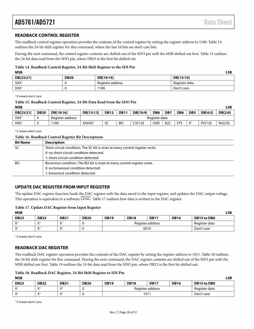
READBACK CONTROL REGISTER The readback control register operation provides the contents of the control register by setting the register address to 1100. Table 14 outlines the 24-bit shift register for this command, where the last 16 bits are don’t care bits.
During the next command, the control register contents are shifted out of the SDO pin with the MSB shifted out first. Table 15 outlines the 24-bit data read from the SDO pin, where DB23 is the first bit shifted out.
Table 14. Readback Control Register, 24-Bit Shift Register to the SDI Pin MSB LSB DB[23:21] DB20 DB[19:16] DB[15:10] XXX1 0 Register address Register data XXX1 0 1100 Don’t care 1 X means don’t care.
Table 15. Readback Control Register, 24-Bit Data Read from the SDO Pin MSB LSB DB[23:21] DB20 DB[19:16] DB[15:13] DB12 DB11 DB[10:9] DB8 DB7 DB6 DB5 DB[4:3] DB[2:0] XXX1 0 Register address Register data XXX1 0 1100 XXXXX1 SC BO CV[1:0] OVR B2C ETS X1 PV[1:0] RA[2:0] 1 X means don’t care.
Table 16. Readback Control Register Bit Descriptions Bit Name Description SC Short-circuit condition. The SC bit is reset at every control register write. 0: no short-circuit condition detected. 1: short-circuit condition detected. BO Brownout condition. The BO bit is reset at every control register write. 0: no brownout condition detected. 1: brownout condition detected.
UPDATE DAC REGISTER FROM INPUT REGISTER The update DAC register function loads the DAC register with the data saved in the input register, and updates the DAC output voltage. This operation is equivalent to a software LDAC. Table 17 outlines how data is written to the DAC register.
Table 17. Update DAC Register from Input Register MSB LSB DB23 DB22 DB21 DB20 DB19 DB18 DB17 DB16 DB15 to DB0 X1 X1 X1 0 Register address Register data X1 X1 X1 0 0010 Don’t care 1 X means don’t care.
READBACK DAC REGISTER The readback DAC register operation provides the contents of the DAC register by setting the register address to 1011. Table 18 outlines the 24-bit shift register for this command. During the next command, the DAC register contents are shifted out of the SDO pin with the MSB shifted out first. Table 19 outlines the 24-bit data read from the SDO pin, where DB23 is the first bit shifted out.
Table 18. Readback DAC Register, 24-Bit Shift Register to SDI Pin MSB LSB DB23 DB22 DB21 DB20 DB19 DB18 DB17 DB16 DB15 to DB0 X1 X1 X1 0 Register address Register data X1 X1 X1 0 1011 Don’t care 1 X means don’t care.

Data Sheet AD5761/AD5721
Rev. C | Page 27 of 31
Table 19. Readback DAC Register, 24-Bit Data Read from SDO Pin MSB LSB DB23 DB22 DB21 DB20 DB19 DB18 DB17 DB16 DB15 to DB0 X1 X1 X1 0 Register address Register data X1 X1 X1 0 1011 Data read from DAC register 1 X means don’t care.
WRITE AND UPDATE DAC REGISTER The write and update DAC register (Register Address 0011) updates the input register and the DAC register with the entered data-word from the input shift register, irrespective of the state of LDAC.
Setting the register address to 0001 writes the input register with the data from the input shift register, clocked in MSB first on the SDI pin.
Table 20. Write and Update DAC Register MSB LSB DB23 DB22 DB21 DB20 DB19 DB18 DB17 DB16 DB15 to DB0 X1 X1 X1 0 Register address Register data X1 X1 X1 0 0001 Data loaded X1 X1 X1 0 0011 Data loaded 1 X means don’t care.
READBACK INPUT REGISTER The readback input register operation provides the contents of the input register by setting the register address to 1010. Table 21 outlines the 24-bit shift register for this command. During the next command, the input register contents are shifted out of the SDO pin with MSB shifted out first. Table 22 outlines the 24-bit data read from the SDO pin, where DB23 is the first bit shifted out.
Table 21. Read Back Input Register, 24-Bit Shift Register to the SDI Pin MSB LSB DB23 DB22 DB21 DB20 DB19 DB18 DB17 DB16 DB15 to DB0 X1 X1 X1 0 Register address Register data X1 X1 X1 0 1010 Don’t care 1 X means don’t care.
Table 22. Readback Input Register, 24-Bit Data Read from the SDO Pin MSB LSB DB23 DB22 DB21 DB20 DB19 DB18 DB17 DB16 DB15 to DB0 X1 X1 X1 0 Register address Register data X1 X1 X1 0 1010 Data read from input register 1 X means don’t care.
DISABLE DAISY-CHAIN FUNCTIONALITY The daisy-chain feature can be disabled to save the power consumed by the SDO buffer when this functionality is not required (see Table 23). When disabled, a readback request is not accepted because the SDO pin remains in tristate.
Table 23. Disable Daisy-Chain Functionality Register MSB LSB DB23 DB22 DB21 DB20 DB19 DB18 DB17 DB16 DB15 to DB1 DB0 X1 X1 X1 0 Register address Register data X1 X1 X1 0 1001 Don’t care DDC 1 X means don’t care.
AD5761/AD5721 Data Sheet
Rev. C | Page 28 of 31
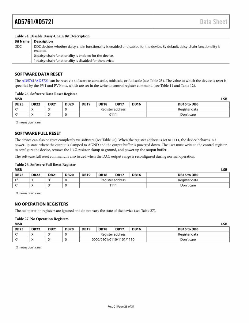
Table 24. Disable Daisy-Chain Bit Description Bit Name Description DDC DDC decides whether daisy-chain functionality is enabled or disabled for the device. By default, daisy-chain functionality is
enabled. 0: daisy-chain functionality is enabled for the device. 1: daisy-chain functionality is disabled for the device.
SOFTWARE DATA RESET The AD5761/AD5721 can be reset via software to zero scale, midscale, or full scale (see Table 25). The value to which the device is reset is specified by the PV1 and PV0 bits, which are set in the write to control register command (see Table 11 and Table 12).
Table 25. Software Data Reset Register MSB LSB DB23 DB22 DB21 DB20 DB19 DB18 DB17 DB16 DB15 to DB0 X1 X1 X1 0 Register address Register data X1 X1 X1 0 0111 Don’t care 1 X means don’t care.
SOFTWARE FULL RESET The device can also be reset completely via software (see Table 26). When the register address is set to 1111, the device behaves in a power-up state, where the output is clamped to AGND and the output buffer is powered down. The user must write to the control register to configure the device, remove the 1 kΩ resistor clamp to ground, and power up the output buffer.
The software full reset command is also issued when the DAC output range is reconfigured during normal operation.
Table 26. Software Full Reset Register MSB LSB DB23 DB22 DB21 DB20 DB19 DB18 DB17 DB16 DB15 to DB0 X1 X1 X1 0 Register address Register data X1 X1 X1 0 1111 Don’t care 1 X means don’t care.
NO OPERATION REGISTERS The no operation registers are ignored and do not vary the state of the device (see Table 27).
Table 27. No Operation Registers MSB LSB DB23 DB22 DB21 DB20 DB19 DB18 DB17 DB16 DB15 to DB0 X1 X1 X1 0 Register address Register data X1 X1 X1 0 0000/0101/0110/1101/1110 Don’t care 1 X means don’t care.
Data Sheet AD5761/AD5721
Rev. C | Page 29 of 31
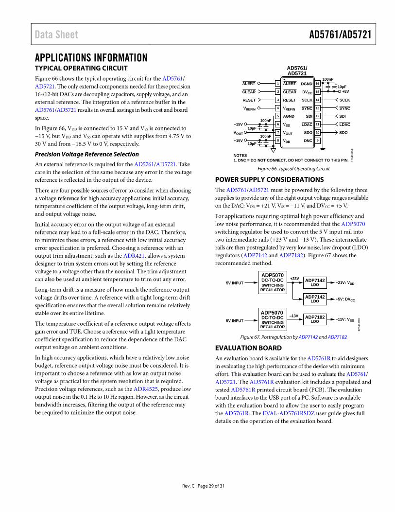
APPLICATIONS INFORMATION TYPICAL OPERATING CIRCUIT Figure 66 shows the typical operating circuit for the AD5761/ AD5721. The only external components needed for these precision 16-/12-bit DACs are decoupling capacitors, supply voltage, and an external reference. The integration of a reference buffer in the AD5761/AD5721 results in overall savings in both cost and board space.
In Figure 66, VDD is connected to 15 V and VSS is connected to −15 V, but VDD and VSS can operate with supplies from 4.75 V to 30 V and from −16.5 V to 0 V, respectively.
Precision Voltage Reference Selection
An external reference is required for the AD5761/AD5721. Take care in the selection of the same because any error in the voltage reference is reflected in the output of the device.
There are four possible sources of error to consider when choosing a voltage reference for high accuracy applications: initial accuracy, temperature coefficient of the output voltage, long-term drift, and output voltage noise.
Initial accuracy error on the output voltage of an external reference may lead to a full-scale error in the DAC. Therefore, to minimize these errors, a reference with low initial accuracy error specification is preferred. Choosing a reference with an output trim adjustment, such as the ADR421, allows a system designer to trim system errors out by setting the reference voltage to a voltage other than the nominal. The trim adjustment can also be used at ambient temperature to trim out any error.
Long-term drift is a measure of how much the reference output voltage drifts over time. A reference with a tight long-term drift specification ensures that the overall solution remains relatively stable over its entire lifetime.
The temperature coefficient of a reference output voltage affects gain error and TUE. Choose a reference with a tight temperature coefficient specification to reduce the dependence of the DAC output voltage on ambient conditions.
In high accuracy applications, which have a relatively low noise budget, reference output voltage noise must be considered. It is important to choose a reference with as low an output noise voltage as practical for the system resolution that is required. Precision voltage references, such as the ADR4525, produce low output noise in the 0.1 Hz to 10 Hz region. However, as the circuit bandwidth increases, filtering the output of the reference may be required to minimize the output noise.
1
2
3
4
5
6
7
8
VOUT
–15V10µF
10µF
100nF
100nF
VREFIN
+15V
16
15
14
13
12
11
10
9
SDI
DGND
SDO
DVCC
DNC
NOTES1. DNC = DO NOT CONNECT. DO NOT CONNECT TO THIS PIN.
SCLK
AD5761/AD5721
SYNC
CLEAR
RESET
LDAC
SDI
SDO
SCLK
SYNC
LDAC
ALERT
AGND
VOUT
VSS
VREFIN
VDD
CLEAR
RESET
ALERT +100nF
10µF+5V
1264
0-06
4
Figure 66. Typical Operating Circuit
POWER SUPPLY CONSIDERATIONS The AD5761/AD5721 must be powered by the following three supplies to provide any of the eight output voltage ranges available on the DAC: VDD = +21 V, VSS = −11 V, and DVCC = +5 V.
For applications requiring optimal high power efficiency and low noise performance, it is recommended that the ADP5070 switching regulator be used to convert the 5 V input rail into two intermediate rails (+23 V and −13 V). These intermediate rails are then postregulated by very low noise, low dropout (LDO) regulators (ADP7142 and ADP7182). Figure 67 shows the recommended method.
ADP7182LDO
ADP5070DC-TO-DCSWITCHING
REGULATOR
–11V: VSS
ADP7142LDO +5V: DVCC
ADP7142LDOSWITCHING
REGULATOR
+21V: VDD
5V INPUT
+23V
–13V
5V INPUT
1264
0-07
0
ADP5070DC-TO-DC
Figure 67. Postregulation by ADP7142 and ADP7182
EVALUATION BOARD An evaluation board is available for the AD5761R to aid designers in evaluating the high performance of the device with minimum effort. This evaluation board can be used to evaluate the AD5761/ AD5721. The AD5761R evaluation kit includes a populated and tested AD5761R printed circuit board (PCB). The evaluation board interfaces to the USB port of a PC. Software is available with the evaluation board to allow the user to easily program the AD5761R. The EVAL-AD5761RSDZ user guide gives full details on the operation of the evaluation board.

AD5761/AD5721 Data Sheet
Rev. C | Page 30 of 31
Table 28. Precision References Recommended for Use with the AD5761/AD5721
Part No. Initial Accuracy (mV Maximum)
Long-Term Drift (ppm Typical)
Temperature Drift (ppm/°C Maximum)
0.1 Hz to 10 Hz Noise (μV p-p Typical)
ADR03 ±2.5 50 3 6 ADR421 ±1 50 3 1.75 ADR431 ±1 40 3 3.5 ADR441 ±1 50 3 1.2 ADR4525 1 25 2 1.25

Data Sheet AD5761/AD5721
Rev. C | Page 31 of 31
OUTLINE DIMENSIONS 0.300.230.18
1.751.60 SQ1.45
3.103.00 SQ2.90
10.50BSC
BOTTOM VIEWTOP VIEW
16
58
9
12
13
4
0.500.400.30
0.05 MAX0.02 NOM
0.20 REF
0.20 MIN
COPLANARITY0.08
PIN 1INDICATOR
0.800.750.70
COMPLIANT TOJEDEC STANDARDS MO-220-WEED-6.PKG
-005
138
SEATINGPLANE
SIDE VIEW
EXPOSEDPAD
02-2
3-20
17-E
PIN 1INDICATOR AREA OPTIONS(SEE DETAIL A)
DETAIL A(JEDEC 95)
FOR PROPER CONNECTION OFTHE EXPOSED PAD, REFER TOTHE PIN CONFIGURATION ANDFUNCTION DESCRIPTIONSSECTION OF THIS DATA SHEET.
Figure 68. 16-Lead Lead Frame Chip Scale Package [LFCSP]
3 mm × 3 mm Body and 0.75 mm Package Height (CP-16-22)
Dimensions shown in millimeters
16 9
81
PIN 1
SEATINGPLANE
8°0°
4.504.404.30
6.40BSC
5.105.004.90
0.65BSC
0.150.05
1.20MAX
0.200.09 0.75
0.600.45
0.300.19
COPLANARITY0.10
COMPLIANT TO JEDEC STANDARDS MO-153-AB Figure 69. 16-Lead Thin Shrink Small Outline Package [TSSOP]
(RU-16) Dimensions shown in millimeters
ORDERING GUIDE Model1 Resolution (Bits) Temperature Range INL (LSB) Package Description Package Option Marking Code AD5721BCPZ-RL7 12 −40°C to +125°C ±0.5 16-Lead LFCSP CP-16-22 DHP AD5721BRUZ 12 −40°C to +125°C ±0.5 16-Lead TSSOP RU-16 AD5721BRUZ-RL7 12 −40°C to +125°C ±0.5 16-Lead TSSOP RU-16 AD5761ACPZ-RL7 16 −40°C to +125°C ±8 16-Lead LFCSP CP-16-22 DN8 AD5761BCPZ-RL7 16 −40°C to +125°C ±2 16-Lead LFCSP CP-16-22 DHQ AD5761ARUZ 16 −40°C to +125°C ±8 16-Lead TSSOP RU-16 AD5761ARUZ-RL7 16 −40°C to +125°C ±8 16-Lead TSSOP RU-16 AD5761BRUZ 16 −40°C to +125°C ±2 16-Lead TSSOP RU-16 AD5761BRUZ-RL7 16 −40°C to +125°C ±2 16-Lead TSSOP RU-16 1 Z = RoHS Compliant Part.
©2015–2018 Analog Devices, Inc. All rights reserved. Trademarks and registered trademarks are the property of their respective owners. D12640-0-1/18(C)