Embed Size (px)
Citation preview
Approval sheet High Capacitance Capacitors
Page 1 of 14 ASC_ High Capacitance_002M_AS Apr. 2011
*Contents in this sheet are subject to change without prior notice.
MULTILAYER CERAMIC CAPACITORS
High Capacitance Series
0402 to 1812 Sizes
X7R, X5R & Y5V Dielectrics
RoHS Compliance
Approval sheet High Capacitance Capacitors
Page 2 of 14 ASC_ High Capacitance_002M_AS Apr. 2011
1. DESCRIPTION
MLCC consists of a conducting material and electrodes. To manufacture a chip-type SMT and achieve miniaturization,
high density and high efficiency, ceramic condensers are used.
WTC high capacitance MLCC offers low ESR and excellent frequency characteristics to be suited for coupling and
decoupling applications in circuit. The high dielectric constant material X7R, X5R and Y5V are used for this series product.
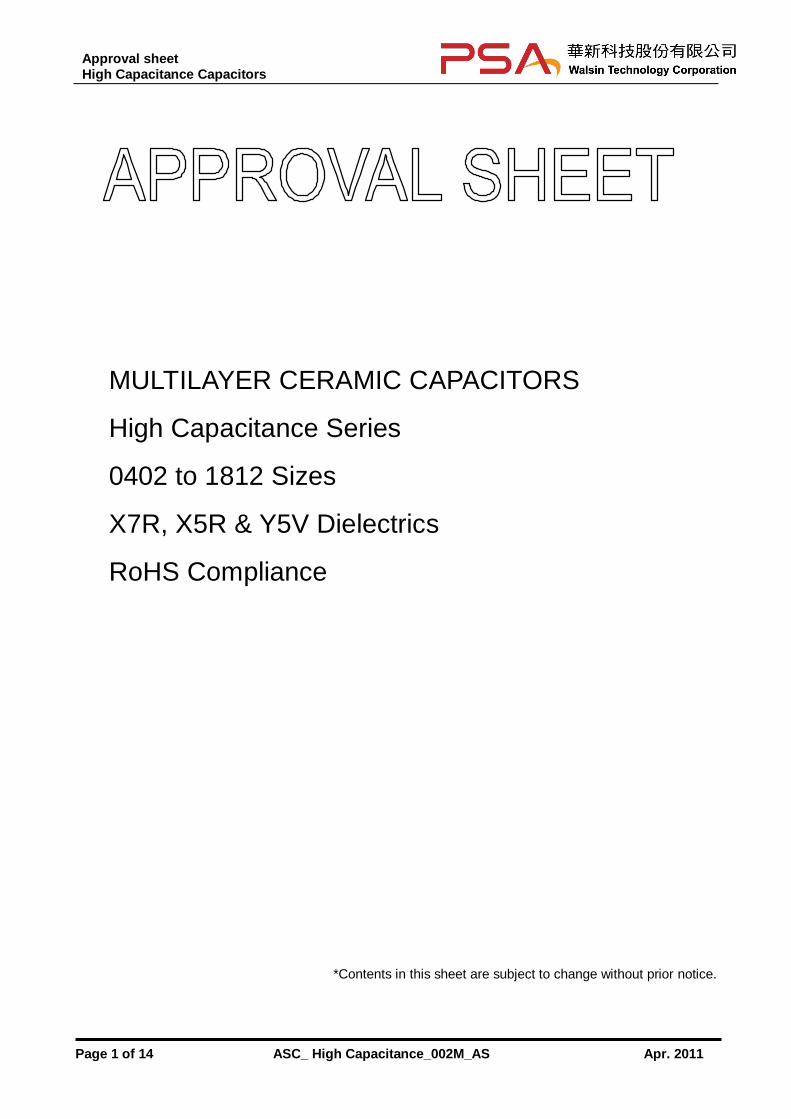
4. HOW TO ORDER
1206 F 106 Z 100 C T
Size
Inch (mm)
0402 (1005)
0603 (1608)
0805 (2012)
1206 (3216)
1210 (3225)
1812 (4532)
Dielectric
B=X7R
X=X5R
F=Y5V
Capacitance
Two significant digits
followed by no. of zeros.
And R is in place of
decimal point.
eg.:
106=10x106
=10μF
Tolerance
K=±10%
M=±20%
Z=-20/+80%
Rated voltage
Two significant digits
followed by no. of
zeros. And R is in
place of decimal
point.
6R3=6.3 VDC
100=10 VDC
160=16 VDC
250=25 VDC
500=50 VDC
101=100 VDC
Termination
C=Cu/Ni/Sn
Packaging
T=7” reeled
G=13” reeled
2. FEATURES
a. Small size with high capacitance.
b. Capacitor with lead-free termination (pure Tin).
3. APPLICATIONS
a. Digital circuit coupling or decoupling applications.
b. For high frequency and high-density type power
suppliers.
c. For bypassing.

Approval sheet High Capacitance Capacitors
Page 3 of 14 ASC_ High Capacitance_002M_AS Apr. 2011
5. EXTERNAL DIMENSIONS
6. GENERAL ELECTRICAL DATA
Dielectric X7R X5R Y5V
Size 0402, 0603, 0805, 1206, 1210, 1812
Capacitance range* 0.56μF to 10μF 0.027μF to 22μF 1μF to 100μF
Capacitance tolerance** K (±10%), M (±20%) Z (-20/+80%)
Rated voltage (WVDC) 6.3V, 10V, 16V, 25V, 50V, 100V
Tan δ* Note 1
Insulation resistance at Ur RxC≥500ΩxF
Operating temperature -55 to +125°C -55 to +85°C -25 to +85°C
Capacitance characteristic ±15% +30/-80%
Termination Ni/Sn (lead-free termination)
* Measured at 1.0±0.2Vrms, 1.0kHz±10% for C≤10μF; 0.5±0.2Vrms, 120Hz±20% for C>10µF, 30~70% related humidity, 25°C ambient
temperature for X7R, X5R and at 20°C for Y5V.
** Preconditioning for Class II MLCC: Perform a heat treatment at 150±10°C for 1 hour, then leave in ambient condition for 24±2 hours
before measurement.
Note 1:
Fig. 1 The outline of MLCC
T
W
L
MB MB
Size
Inch (mm) L (mm) W (mm) T (mm)/Symbol Remark MB (mm)
0402 (1005) 1.00±0.05 0.50±0.05 0.50±0.05 N # 0.25
+0.05/-0.10
0603 (1608) 1.60±0.10 0.80±0.10 0.80±0.07 S
0.40±0.15 1.60+0.15/-0.10 0.80+0.15/-0.10 0.80+0.15/-0.10 X
0805 (2012) 2.00±0.15 1.25±0.10
0.80±0.10 B
0.50±0.20 1.25±0.10 D #
2.00±0.20 1.25±0.20 1.25±0.20 I #
1206 (3216)
3.20±0.15 1.60±0.15 0.95±0.10 C #
0.60±0.20
1.25±0.10 D #
3.20±0.20 1.60±0.20 1.60±0.20 G #
1.15±0.15 J #
3.20+0.30/-0.10 1.60+0.30/-0.10 1.60+0.30/-0.10 P #
1210 (3225)
3.20±0.30 2.50±0.20 0.95±0.10 C #
0.75±0.25
1.25±0.10 D #
3.20±0.40 2.50±0.30
1.60±0.20 G #
2.00±0.20 K #
2.50±0.30 M #
1812 (4532) 4.50±0.40 3.20±0.30
1.25±0.10 D #
0.75±0.25 2.00±0.20 K #
4.50±0.40 3.20±0.40 2.50±0.30 M #
# Reflow soldering only is recommended.
X7R/X5R
Rated vol. D.F.≦ Exception of D.F. ≦
≧50V 2.5% 3% 0603≧0.047F; 0805≧0.18F;1206≧0.47F
25V 3.5%
5% 0805≧1F; 1210≧10F
7% 0603≧0.33F; 1206≧4.7F
10% 0402≧0.10F;0603≧0.47F; 0805≧2.2F; 1206≧6.8F
16V 3.5% 5%
0402≧0.033F; 0603≧0.15F; 0805≧0.68F;1206≧2.2F;1210≧4.7F
10% 0603≧0.68F;0805≧2.2F; 1206≧4.7F;1210≧22F
10V 5% 10%
0402≧0.33F;0603≧0.33F; 0805≧2.2F;1206≧2.2F;1210≧22F;
15% 0201≧0.1F; 0402≧1F
6.3V 10% 15%
0603≧10F; 0805≧4.7F; 1206≧ 47μF; 1210≧100F;
20% 0402≧2.2F
Y5V
Rated vol. D.F.≦ Exception of D.F.≦
≧50V 5% 7% 0603≧0.1F; 0805≧0.47F; 1206≧4.7F
35V 7% --- ---
25V 5% 7%
0402≧0.047F;0603≧0.1F; 0805≧0.33F;1206≧1F; 1210≧4.7F
9% 0402≧0.068F;0603≧0.47F; 1206≧4.7F; 1210≧22F
16V (C<1.0F)
7% 9% 0402≧0.068F; 0603≧0.68F
12.5% 0402≧0.22F
16V (C≧1.0F)
9% 12.5% 0603≧2.2F; 0805≧3.3F; 1206≧10F; 1210≧22F; 1812≧47F
10V 12.5% 20% 0402≧0.47F
6.3V 20% --- ---

Approval sheet High Capacitance Capacitors
Page 4 of 14 ASC_ High Capacitance_002M_AS Apr. 2011
7. CAPACITANCE RANGE
7-1 X7R Dielectric
DIELECTRIC X7R
SIZE 0603 0805 1206 1210 1812
RATED VOLTAGE
(VDC)
6.3 10 16 6.3 10 16 25 6.3 10 16 25 50 10 16 25 50 100 10 16 25 50 100
Cap
acit
an
ce
0.56μF (564) X X
0.68μF (684) X X
0.82μF (824) X X
1.0μF (105) X X X D D D J J J P D D D D K D D D K K
1.5μF (155) I J J J P K
2.2μF (225) I I I I J J J P K G M
3.3μF (335) P P P G
4.7μF (475) I I P P P P K K K
6.8μF (685)
10μF (106) I P P P K K K M M M
1. The letter in cell is expressed the symbol of product thickness.
7-2 X5R Dielectric
Dielectric X5R
Size 0402 0603 0805 1206 1210 1812
Rated Voltage (VDC) 6.3 10 16 25 6.3 10 16 25 6.3 10 16 25 6.3 10 16 25 6.3 10 16 25 6.3
Capacitance
0.027μF (273) N
0.033μF (333) N
0.039μF (393) N
0.047μF (473) N
0.056μF (563) N N
0.068μF (683) N N
0.082μF (823) N N N
0.10μF (104) N N N N
0.15μF (154)
0.22μF (224) N N N X X
0.27uF (274) X X
0.33μF (334) N N X X X X
0.39μF (394) X X
0.47μF (474) N N X X X
0.68μF (684) N N X X X
0.82uF (824) X X X
1.0μF (105) N N X X X X
1.5μF (155) X I I J J K K
2.2μF (225) N X X X I I I I J J P K K
3.3μF (335) I I I I P P P
4.7μF (475) N X X I I I I P P P P K K K
6.8uF (685) P P
10μF (106) X I I I P P P P K K K K
22μF (226) I I P P M M M
47μF (476) I P M M M
100μF (107) M U
1. The letter in cell is expressed the symbol of product thickness.

Approval sheet High Capacitance Capacitors
Page 5 of 14 ASC_ High Capacitance_002M_AS Apr. 2011
7-3 Y5V Dielectric
DIELECTRIC Y5V
SIZE 0402 0603 0805
RATED VOLTAGE (VDC) 6.3 10 6.3 10 16 25 6.3 10 16 25 50
Cap
acit
an
ce
1.0μF (105) N N S X X B B D D
1.5μF (155) S D D
2.2μF (225) S S X D D I I
3.3μF (335) D D
4.7μF (475) X X D D I
6.8μF (685) I
10μF (106) I I I
22μF (226) I
DIELECTRIC Y5V
SIZE 1206 1210 1812
RATED VOLTAGE (VDC) 10 16 25 35 50 6.3 10 16 25 35 50 6.3 10 16 25 50 100
Cap
acit
an
ce
1.0μF (105) C C C C C C C C D D D D D
1.5μF (155) C C C C C C D D D D
2.2μF (225) C C C J C C C G D D D D
3.3μF (335) J J J C C C D D D D
4.7μF (475) J J J J P C C D G D D D D
6.8μF (685) J J C C D D D D D
10μF (106) J J P D D G K G D D D K
22μF (226) P P K K K
47μF (476) P K K M
100μF (107) M
1. The letter in cell is expressed the symbol of product thickness.
8. PACKAGING STYLE AND QUANTITY
Size Thickness (mm)/Symbol Paper tape Plastic tape
7” reel 13” reel 7” reel 13” reel
0402 (1005) 0.50±0.05 N 10k 50k - -
0603 (1608) 0.80±0.07 S 4k 15k - -
0.80+0.15/-0.10 X 4k 15k - -
0805 (2012)
0.80±0.10 B 4k 15k - -
1.25±0.10 D - - 3k 10k
1.25±0.20 I - - 3k 10k
1206 (3216)
0.95±0.10 C - - 3k 10k
1.15±0.15 J - - 3K 10K
1.25±0.10 D - - 3k 10k
1.60±0.20 G - - 2k -
1.60+0.30/-0.10 P - - 2k -
1210 (3225)
0.95±0.10 C - - 3k 10k
1.25±0.10 D - - 3k 10k
1.60±0.20 G - - 2k -
2.00±0.20 K - - 1k -
2.50±0.30 M - - 1k -
1812 (4532)
1.25±0.10 D - - 1k -
2.00±0.20 K - - 1k -
2.50±0.30 M - - 0.5k
Unit: pieces

Approval sheet High Capacitance Capacitors
Page 6 of 14 ASC_ High Capacitance_002M_AS Apr. 2011
9. ELECTRICAL CHARACTERISTICS
Typical Impedance/ESR vs. Frequency
Fig. 2 ESR and IZI vs. frequency (1206X106_10V)
1206X106_10V
0.001
0.01
0.1
1
10
100
1000
1 10 100 1,000 10,000
Frequency (kHz)
Ohm I Z I
ESR
Fig. 3 ESR and IZI vs. frequency (0805F106_10V)
0805F106_10V
0.001
0.01
0.1
1
10
100
1000
1 10 100 1,000 10,000
Frequency (kHz)
Ohm I Z I
ESR
Fig. 5 ESR and IZI vs. frequency (0603X105_10V)
0603X105_10V
0.001
0.01
0.1
1
10
100
1000
10000
1 10 100 1,000 10,000
Frequency (kHz)
Ohm I Z I
ESR
Fig. 4 ESR and IZI vs. frequency (0805F475_10V)
0805F475_10V
0.01
0.1
1
10
100
1000
1 10 100 1,000 10,000 100,000
Frequency (kHz)
Ohm
I Z I
ESR
Approval sheet High Capacitance Capacitors
Page 7 of 14 ASC_ High Capacitance_002M_AS Apr. 2011
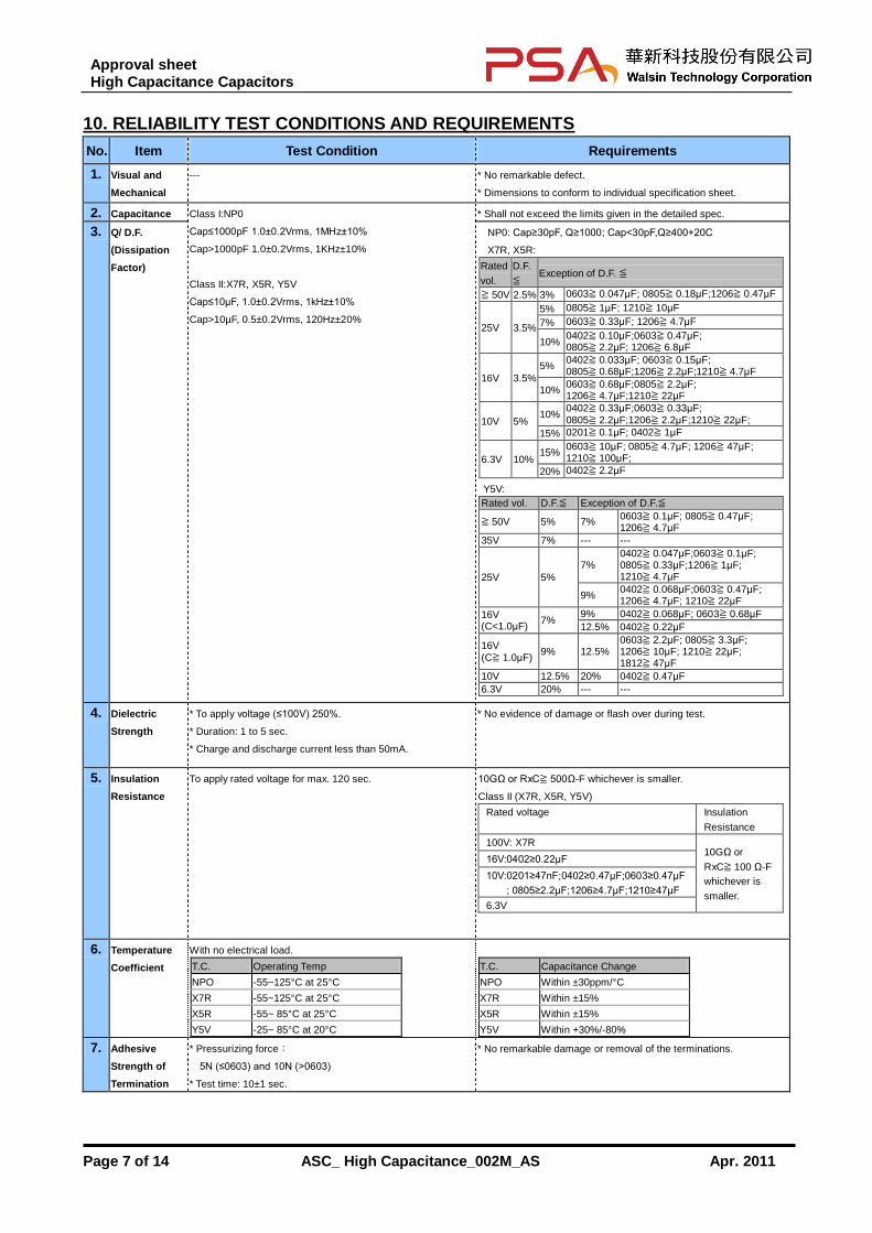
10. RELIABILITY TEST CONDITIONS AND REQUIREMENTS
No. Item Test Condition Requirements
1. Visual and
Mechanical
--- * No remarkable defect.
* Dimensions to conform to individual specification sheet.
2. Capacitance Class I:NP0
Cap≤1000pF 1.0±0.2Vrms, 1MHz±10%
Cap>1000pF 1.0±0.2Vrms, 1KHz±10%
Class II:X7R, X5R, Y5V
Cap≤10µF, 1.0±0.2Vrms, 1kHz±10%
Cap>10µF, 0.5±0.2Vrms, 120Hz±20%
* Shall not exceed the limits given in the detailed spec.
3. Q/ D.F.
(Dissipation
Factor)
NP0: Cap≥30pF, Q≥1000; Cap<30pF,Q≥400+20C
X7R, X5R:
Rated
vol.
D.F.
≦ Exception of D.F. ≦
≧ 50V 2.5% 3% 0603≧ 0.047μF; 0805≧ 0.18μF;1206≧ 0.47μF
25V 3.5%
5% 0805≧ 1μF; 1210≧ 10μF
7% 0603≧ 0.33μF; 1206≧ 4.7μF
10% 0402≧ 0.10μF;0603≧ 0.47μF; 0805≧ 2.2μF; 1206≧ 6.8μF
16V 3.5%
5% 0402≧ 0.033μF; 0603≧ 0.15μF; 0805≧ 0.68μF;1206≧ 2.2μF;1210≧ 4.7μF
10% 0603≧ 0.68μF;0805≧ 2.2μF; 1206≧ 4.7μF;1210≧ 22μF
10V 5% 10%
0402≧ 0.33μF;0603≧ 0.33μF; 0805≧ 2.2μF;1206≧ 2.2μF;1210≧ 22μF;
15% 0201≧ 0.1μF; 0402≧ 1μF
6.3V 10% 15%
0603≧ 10μF; 0805≧ 4.7μF; 1206≧ 47μF; 1210≧ 100μF;
20% 0402≧ 2.2μF
Y5V:
Rated vol. D.F.≦ Exception of D.F.≦
≧ 50V 5% 7% 0603≧ 0.1μF; 0805≧ 0.47μF; 1206≧ 4.7μF
35V 7% --- ---
25V 5%
7% 0402≧ 0.047μF;0603≧ 0.1μF; 0805≧ 0.33μF;1206≧ 1μF; 1210≧ 4.7μF
9% 0402≧ 0.068μF;0603≧ 0.47μF; 1206≧ 4.7μF; 1210≧ 22μF
16V (C<1.0μF)
7% 9% 0402≧ 0.068μF; 0603≧ 0.68μF
12.5% 0402≧ 0.22μF
16V (C≧ 1.0μF)
9% 12.5% 0603≧ 2.2μF; 0805≧ 3.3μF; 1206≧ 10μF; 1210≧ 22μF; 1812≧ 47μF
10V 12.5% 20% 0402≧ 0.47μF
6.3V 20% --- ---
4. Dielectric
Strength
* To apply voltage (≤100V) 250%.
* Duration: 1 to 5 sec.
* Charge and discharge current less than 50mA.
* No evidence of damage or flash over during test.
5. Insulation
Resistance
To apply rated voltage for max. 120 sec. 10GΩ or RxC≧ 500Ω-F whichever is smaller.
Class II (X7R, X5R, Y5V)
Rated voltage Insulation
Resistance
100V: X7R 10GΩ or
RxC≧ 100 Ω-F
whichever is
smaller.
16V:0402≥0.22µF
10V:0201≥47nF;0402≥0.47µF;0603≥0.47µF
; 0805≥2.2µF;1206≥4.7µF;1210≥47µF
6.3V
6. Temperature
Coefficient
With no electrical load.
T.C. Operating Temp
NPO -55~125°C at 25°C
X7R -55~125°C at 25°C
X5R -55~ 85°C at 25°C
Y5V -25~ 85°C at 20°C
T.C. Capacitance Change
NPO Within ±30ppm/°C
X7R Within ±15%
X5R Within ±15%
Y5V Within +30%/-80%
7. Adhesive
Strength of
Termination
* Pressurizing force:
5N (≤0603) and 10N (>0603)
* Test time: 10±1 sec.
* No remarkable damage or removal of the terminations.
Approval sheet High Capacitance Capacitors
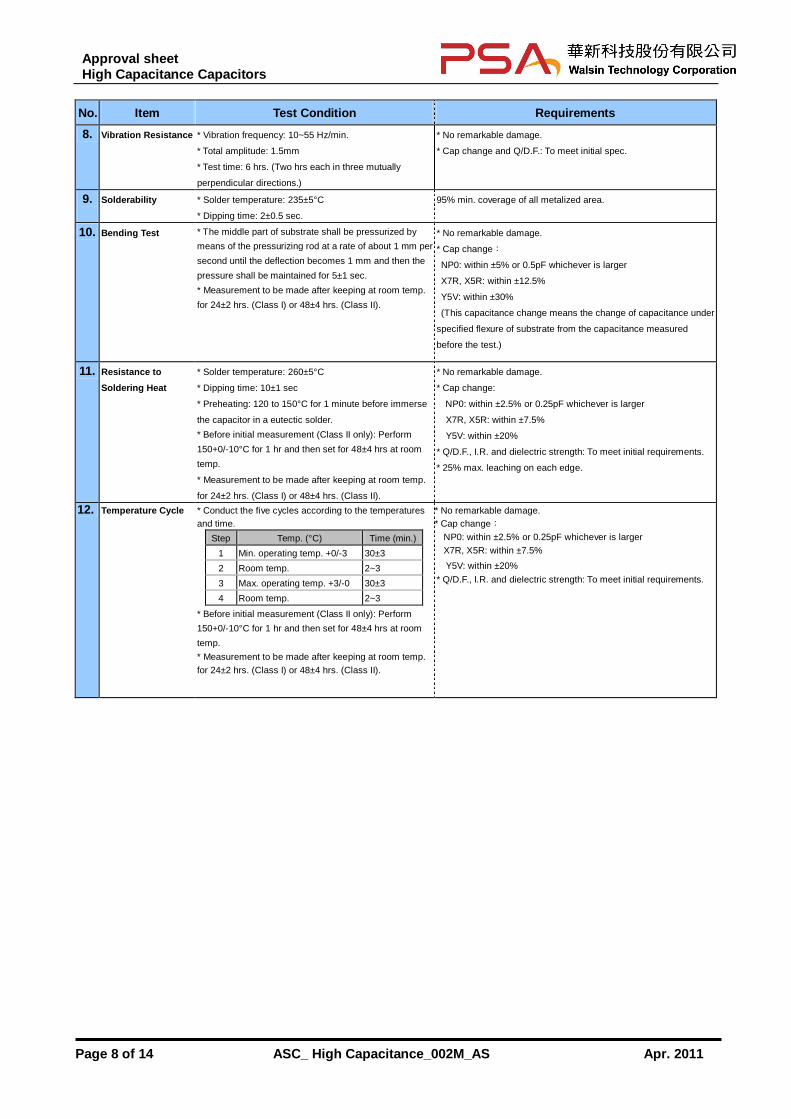
Page 8 of 14 ASC_ High Capacitance_002M_AS Apr. 2011
No. Item Test Condition Requirements
8. Vibration Resistance * Vibration frequency: 10~55 Hz/min.
* Total amplitude: 1.5mm
* Test time: 6 hrs. (Two hrs each in three mutually
perpendicular directions.)
* No remarkable damage.
* Cap change and Q/D.F.: To meet initial spec.
9.
Solderability * Solder temperature: 235±5°C
* Dipping time: 2±0.5 sec.
95% min. coverage of all metalized area.
10. Bending Test * The middle part of substrate shall be pressurized by
means of the pressurizing rod at a rate of about 1 mm per
second until the deflection becomes 1 mm and then the
pressure shall be maintained for 5±1 sec.
* Measurement to be made after keeping at room temp.
for 24±2 hrs. (Class I) or 48±4 hrs. (Class II).
* No remarkable damage.
* Cap change:
NP0: within ±5% or 0.5pF whichever is larger
X7R, X5R: within ±12.5%
Y5V: within ±30%
(This capacitance change means the change of capacitance under
specified flexure of substrate from the capacitance measured
before the test.)
11. Resistance to
Soldering Heat
* Solder temperature: 260±5°C
* Dipping time: 10±1 sec
* Preheating: 120 to 150°C for 1 minute before immerse
the capacitor in a eutectic solder.
* Before initial measurement (Class II only): Perform
150+0/-10°C for 1 hr and then set for 48±4 hrs at room
temp.
* Measurement to be made after keeping at room temp.
for 24±2 hrs. (Class I) or 48±4 hrs. (Class II).
* No remarkable damage.
* Cap change:
NP0: within ±2.5% or 0.25pF whichever is larger
X7R, X5R: within ±7.5%
Y5V: within ±20%
* Q/D.F., I.R. and dielectric strength: To meet initial requirements.
* 25% max. leaching on each edge.
12. Temperature Cycle * Conduct the five cycles according to the temperatures
and time.
Step Temp. (°C) Time (min.)
1 Min. operating temp. +0/-3 30±3
2 Room temp. 2~3
3 Max. operating temp. +3/-0 30±3
4 Room temp. 2~3
* Before initial measurement (Class II only): Perform
150+0/-10°C for 1 hr and then set for 48±4 hrs at room
temp.
* Measurement to be made after keeping at room temp.
for 24±2 hrs. (Class I) or 48±4 hrs. (Class II).
* No remarkable damage.
* Cap change:
NP0: within ±2.5% or 0.25pF whichever is larger
X7R, X5R: within ±7.5%
Y5V: within ±20%
* Q/D.F., I.R. and dielectric strength: To meet initial requirements.

Approval sheet High Capacitance Capacitors
Page 9 of 14 ASC_ High Capacitance_002M_AS Apr. 2011
No. Item Test Condition Requirements
13. Humidity (Damp
Heat) Steady State
* Test temp.: 40±2°C
* Humidity: 90~95% RH
* Test time: 500+24/-0hrs.
* Measurement to be made after keeping at room temp.
for 24±2 hrs. (Class I) or 48±4 hrs. (Class II).
* No remarkable damage.
* Cap change:
NP0: within ±5% or 0.5pF whichever is larger
X7R, X5R: ≥10V, within ±12.5%; 6.3V, within ±25%
Y5V: ≥10V, within ±30%; 6.3V, within +30/-40%
* Q/D.F. value:
NP0: More than 30pF Q≥350, 10pF≤C≤30pF, Q≥275+2.5C
Less than 10pF Q≥200+10C
X7R, X5R:
Rated
vol. D.F.≦ Exception of D.F.≦
≧ 50V 3% 6% 0603≧ 0.047μF; 0805≧ 0.18μF; 1206≧ 0.47μF
25V 5%
10% 0805≧ 1μF; 1210≧ 10μF
14% 0603≧ 0.33μF;1206≧ 4.7μF
15% 0402≧ 0.10μF; 0603≧ 0.47μF; 0805≧ 2.2μF; 1206≧ 6.8μF
16V 5% 10%
0603≧ 0.15μF; 0805≧ 0.68μF; 1206≧ 2.2μF; 1210≧ 4.7μF,
15% 0402≧ 0.033μF; 0603≧ 0.68μF;0805≧ 2.2μF 1206≧ 4.7μF; 1210≧ 22μF
10V 7.5% 15%
0402≧ 0.33μF; 0603≧ 0.33μF;0805≧ 2.2μF 1206≧ 2.2μF; 1210≧ 22μF
20% 0201≧ 0.1μF ;0402≧ 1μF
6.3V 15% 30% 0402≧ 2.2μF ;0603≧ 10μF; 0805≧ 4.7μF; 1206≧ 47μF;1210≧ 100μF
Y5V:
Rated vol. D.F.≦ Exception of D.F.≦
≧ 50V 7.5% 10% 0603≧ 0.1μF; 0805≧ 0.47μF; 1206≧ 4.7μF
35V 10% --- ---
25V 7.5%
10% 0402≧ 0.047μF;0603≧ 0.1μF; 0805≧ 0.33μF;1206≧ 1μF;
1210≧ 4.7μF
15% 0402≧ 0.068μF;0603≧ 0.47μF; 1206≧ 4.7μF; 1210≧ 22μF
16V (C<1.0μF)
10% 12.5% 0402≧ 0.068μF; 0603≧ 0.68μF
20% 0402≧ 0.22μF
16V (C≧ 1.0μF)
12.5% 20% 0603≧ 2.2μF; 0805≧ 3.3μF; 1206≧ 10μF;1210≧ 22μF; 1812≧ 47μF;
10V 20% 30% 0402≧ 0.47μF
6.3V 30% --- ---
*I.R.: ≥10V, 1GΩ or 50 Ω-F whichever is smaller.
Class II (X7R, X5R, Y5V)
Rated voltage Insulation
Resistance
100V: X7R 1GΩ or
RxC≧ 10 Ω-F
whichever is
smaller.
16V:0402≥0.22µF
10V:0201≥47nF;0402≥0.47µF;0603≥0.47µF
; 0805≥2.2µF;1206≥4.7µF;1210≥47µF
6.3V
Approval sheet High Capacitance Capacitors
Page 10 of 14 ASC_ High Capacitance_002M_AS Apr. 2011
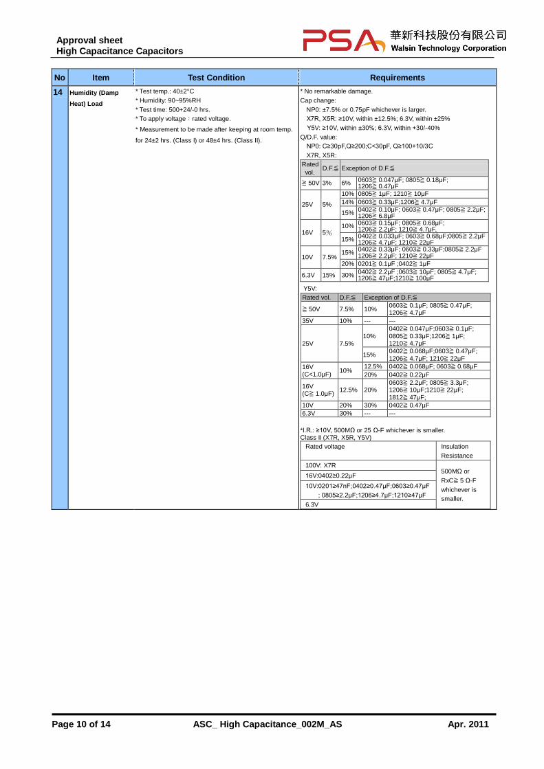
No Item Test Condition Requirements
14 Humidity (Damp
Heat) Load
* Test temp.: 40±2°C
* Humidity: 90~95%RH
* Test time: 500+24/-0 hrs.
* To apply voltage:rated voltage.
* Measurement to be made after keeping at room temp.
for 24±2 hrs. (Class I) or 48±4 hrs. (Class II).
* No remarkable damage.
Cap change:
NP0: ±7.5% or 0.75pF whichever is larger.
X7R, X5R: ≥10V, within ±12.5%; 6.3V, within ±25%
Y5V: ≥10V, within ±30%; 6.3V, within +30/-40%
Q/D.F. value:
NP0: C≥30pF,Q≥200;C<30pF, Q≥100+10/3C
X7R, X5R:
Rated
vol. D.F.≦ Exception of D.F.≦
≧ 50V 3% 6% 0603≧ 0.047μF; 0805≧ 0.18μF; 1206≧ 0.47μF
25V 5%
10% 0805≧ 1μF; 1210≧ 10μF
14% 0603≧ 0.33μF;1206≧ 4.7μF
15% 0402≧ 0.10μF; 0603≧ 0.47μF; 0805≧ 2.2μF; 1206≧ 6.8μF
16V 5% 10%
0603≧ 0.15μF; 0805≧ 0.68μF; 1206≧ 2.2μF; 1210≧ 4.7μF,
15% 0402≧ 0.033μF; 0603≧ 0.68μF;0805≧ 2.2μF 1206≧ 4.7μF; 1210≧ 22μF
10V 7.5% 15%
0402≧ 0.33μF; 0603≧ 0.33μF;0805≧ 2.2μF 1206≧ 2.2μF; 1210≧ 22μF
20% 0201≧ 0.1μF ;0402≧ 1μF
6.3V 15% 30% 0402≧ 2.2μF ;0603≧ 10μF; 0805≧ 4.7μF; 1206≧ 47μF;1210≧ 100μF
Y5V:
Rated vol. D.F.≦ Exception of D.F.≦
≧ 50V 7.5% 10% 0603≧ 0.1μF; 0805≧ 0.47μF; 1206≧ 4.7μF
35V 10% --- ---
25V 7.5% 10%
0402≧ 0.047μF;0603≧ 0.1μF; 0805≧ 0.33μF;1206≧ 1μF; 1210≧ 4.7μF
15% 0402≧ 0.068μF;0603≧ 0.47μF;
1206≧ 4.7μF; 1210≧ 22μF
16V (C<1.0μF)
10% 12.5% 0402≧ 0.068μF; 0603≧ 0.68μF
20% 0402≧ 0.22μF
16V (C≧ 1.0μF)
12.5% 20% 0603≧ 2.2μF; 0805≧ 3.3μF; 1206≧ 10μF;1210≧ 22μF; 1812≧ 47μF;
10V 20% 30% 0402≧ 0.47μF
6.3V 30% --- ---
*I.R.: ≥10V, 500MΩ or 25 Ω-F whichever is smaller. Class II (X7R, X5R, Y5V)
Rated voltage Insulation
Resistance
100V: X7R 500MΩ or
RxC≧ 5 Ω-F
whichever is
smaller.
16V:0402≥0.22µF
10V:0201≥47nF;0402≥0.47µF;0603≥0.47µF
; 0805≥2.2µF;1206≥4.7µF;1210≥47µF
6.3V
Approval sheet High Capacitance Capacitors
Page 11 of 14 ASC_ High Capacitance_002M_AS Apr. 2011
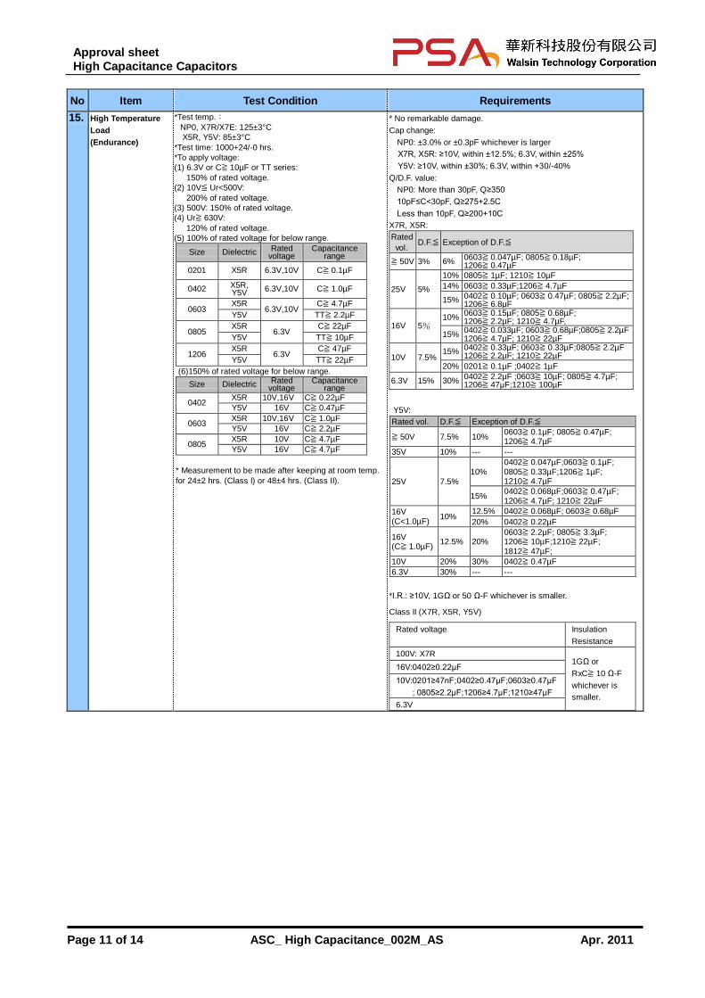
No Item Test Condition Requirements
15. High Temperature
Load
(Endurance)
*Test temp.:
NP0, X7R/X7E: 125±3°C
X5R, Y5V: 85±3°C
*Test time: 1000+24/-0 hrs.
*To apply voltage:
(1) 6.3V or C≧ 10µF or TT series:
150% of rated voltage.
(2) 10V≦ Ur<500V:
200% of rated voltage.
(3) 500V: 150% of rated voltage.
(4) Ur≧ 630V:
120% of rated voltage.
(5) 100% of rated voltage for below range.
Size Dielectric Rated voltage
Capacitance range
0201 X5R 6.3V,10V C≧ 0.1µF
0402 X5R, Y5V
6.3V,10V C≧ 1.0µF
0603 X5R
6.3V,10V C≧ 4.7µF
Y5V TT≧ 2.2µF
0805 X5R
6.3V C≧ 22µF
Y5V TT≧ 10µF
1206 X5R
6.3V C≧ 47µF
Y5V TT≧ 22µF
(6)150% of rated voltage for below range.
Size Dielectric Rated voltage
Capacitance range
0402 X5R 10V,16V C≧ 0.22µF
Y5V 16V C≧ 0.47µF
0603 X5R 10V,16V C≧ 1.0µF
Y5V 16V C≧ 2.2µF
0805 X5R 10V C≧ 4.7µF
Y5V 16V C≧ 4.7µF
* Measurement to be made after keeping at room temp.
for 24±2 hrs. (Class I) or 48±4 hrs. (Class II).
* No remarkable damage.
Cap change:
NP0: ±3.0% or ±0.3pF whichever is larger
X7R, X5R: ≥10V, within ±12.5%; 6.3V, within ±25%
Y5V: ≥10V, within ±30%; 6.3V, within +30/-40%
Q/D.F. value:
NP0: More than 30pF, Q≥350
10pF≤C<30pF, Q≥275+2.5C
Less than 10pF, Q≥200+10C
X7R, X5R:
Rated
vol. D.F.≦ Exception of D.F.≦
≧ 50V 3% 6% 0603≧ 0.047µF; 0805≧ 0.18µF; 1206≧ 0.47µF
25V 5%
10% 0805≧ 1µF; 1210≧ 10µF
14% 0603≧ 0.33µF;1206≧ 4.7µF
15% 0402≧ 0.10µF; 0603≧ 0.47µF; 0805≧ 2.2µF; 1206≧ 6.8µF
16V 5% 10%
0603≧ 0.15µF; 0805≧ 0.68µF; 1206≧ 2.2µF; 1210≧ 4.7µF,
15% 0402≧ 0.033µF; 0603≧ 0.68µF;0805≧ 2.2µF 1206≧ 4.7µF; 1210≧ 22µF
10V 7.5% 15%
0402≧ 0.33µF; 0603≧ 0.33µF;0805≧ 2.2µF 1206≧ 2.2µF; 1210≧ 22µF
20% 0201≧ 0.1µF ;0402≧ 1µF
6.3V 15% 30% 0402≧ 2.2µF ;0603≧ 10µF; 0805≧ 4.7µF; 1206≧ 47μF;1210≧ 100µF
Y5V:
Rated vol. D.F.≦ Exception of D.F.≦
≧ 50V 7.5% 10% 0603≧ 0.1µF; 0805≧ 0.47µF; 1206≧ 4.7µF
35V 10% --- ---
25V 7.5% 10%
0402≧ 0.047µF;0603≧ 0.1µF; 0805≧ 0.33µF;1206≧ 1µF; 1210≧ 4.7µF
15% 0402≧ 0.068µF;0603≧ 0.47µF; 1206≧ 4.7µF; 1210≧ 22µF
16V (C<1.0µF)
10% 12.5% 0402≧ 0.068µF; 0603≧ 0.68µF
20% 0402≧ 0.22µF
16V (C≧ 1.0µF)
12.5% 20% 0603≧ 2.2µF; 0805≧ 3.3µF; 1206≧ 10µF;1210≧ 22µF; 1812≧ 47µF;
10V 20% 30% 0402≧ 0.47µF
6.3V 30% --- ---
*I.R.: ≥10V, 1GΩ or 50 Ω-F whichever is smaller.
Class II (X7R, X5R, Y5V)
Rated voltage Insulation
Resistance
100V: X7R 1GΩ or
RxC≧ 10 Ω-F
whichever is
smaller.
16V:0402≥0.22µF
10V:0201≥47nF;0402≥0.47µF;0603≥0.47µF
; 0805≥2.2µF;1206≥4.7µF;1210≥47µF
6.3V
Approval sheet High Capacitance Capacitors
Page 12 of 14 ASC_ High Capacitance_002M_AS Apr. 2011
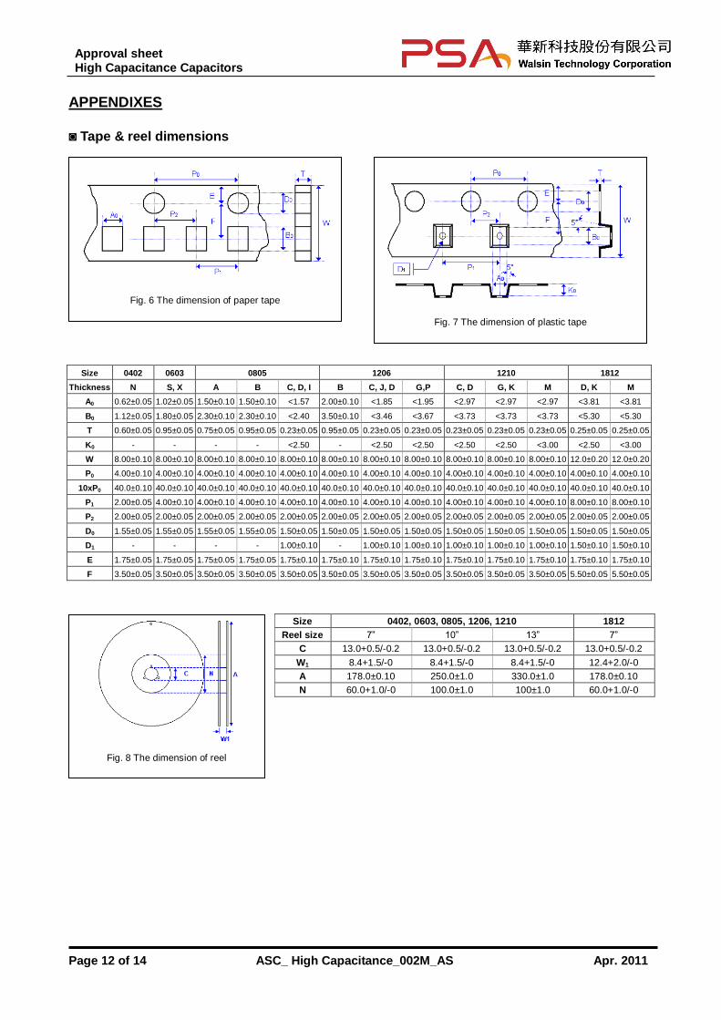
APPENDIXES
Tape & reel dimensions
Size 0402 0603 0805 1206 1210 1812
Thickness N S, X A B C, D, I B C, J, D G,P C, D G, K M D, K M
A0 0.62±0.05 1.02±0.05 1.50±0.10 1.50±0.10 <1.57 2.00±0.10 <1.85 <1.95 <2.97 <2.97 <2.97 <3.81 <3.81
B0 1.12±0.05 1.80±0.05 2.30±0.10 2.30±0.10 <2.40 3.50±0.10 <3.46 <3.67 <3.73 <3.73 <3.73 <5.30 <5.30
T 0.60±0.05 0.95±0.05 0.75±0.05 0.95±0.05 0.23±0.05 0.95±0.05 0.23±0.05 0.23±0.05 0.23±0.05 0.23±0.05 0.23±0.05 0.25±0.05 0.25±0.05
K0 - - - - <2.50 - <2.50 <2.50 <2.50 <2.50 <3.00 <2.50 <3.00
W 8.00±0.10 8.00±0.10 8.00±0.10 8.00±0.10 8.00±0.10 8.00±0.10 8.00±0.10 8.00±0.10 8.00±0.10 8.00±0.10 8.00±0.10 12.0±0.20 12.0±0.20
P0 4.00±0.10 4.00±0.10 4.00±0.10 4.00±0.10 4.00±0.10 4.00±0.10 4.00±0.10 4.00±0.10 4.00±0.10 4.00±0.10 4.00±0.10 4.00±0.10 4.00±0.10
10xP0 40.0±0.10 40.0±0.10 40.0±0.10 40.0±0.10 40.0±0.10 40.0±0.10 40.0±0.10 40.0±0.10 40.0±0.10 40.0±0.10 40.0±0.10 40.0±0.10 40.0±0.10
P1 2.00±0.05 4.00±0.10 4.00±0.10 4.00±0.10 4.00±0.10 4.00±0.10 4.00±0.10 4.00±0.10 4.00±0.10 4.00±0.10 4.00±0.10 8.00±0.10 8.00±0.10
P2 2.00±0.05 2.00±0.05 2.00±0.05 2.00±0.05 2.00±0.05 2.00±0.05 2.00±0.05 2.00±0.05 2.00±0.05 2.00±0.05 2.00±0.05 2.00±0.05 2.00±0.05
D0 1.55±0.05 1.55±0.05 1.55±0.05 1.55±0.05 1.50±0.05 1.50±0.05 1.50±0.05 1.50±0.05 1.50±0.05 1.50±0.05 1.50±0.05 1.50±0.05 1.50±0.05
D1 - - - - 1.00±0.10 - 1.00±0.10 1.00±0.10 1.00±0.10 1.00±0.10 1.00±0.10 1.50±0.10 1.50±0.10
E 1.75±0.05 1.75±0.05 1.75±0.05 1.75±0.05 1.75±0.10 1.75±0.10 1.75±0.10 1.75±0.10 1.75±0.10 1.75±0.10 1.75±0.10 1.75±0.10 1.75±0.10
F 3.50±0.05 3.50±0.05 3.50±0.05 3.50±0.05 3.50±0.05 3.50±0.05 3.50±0.05 3.50±0.05 3.50±0.05 3.50±0.05 3.50±0.05 5.50±0.05 5.50±0.05
Fig. 7 The dimension of plastic tape
Fig. 8 The dimension of reel
Fig. 6 The dimension of paper tape
Size 0402, 0603, 0805, 1206, 1210 1812
Reel size 7” 10” 13” 7”
C 13.0+0.5/-0.2 13.0+0.5/-0.2 13.0+0.5/-0.2 13.0+0.5/-0.2
W1 8.4+1.5/-0 8.4+1.5/-0 8.4+1.5/-0 12.4+2.0/-0
A 178.0±0.10 250.0±1.0 330.0±1.0 178.0±0.10
N 60.0+1.0/-0 100.0±1.0 100±1.0 60.0+1.0/-0
Approval sheet High Capacitance Capacitors
Page 13 of 14 ASC_ High Capacitance_002M_AS Apr. 2011
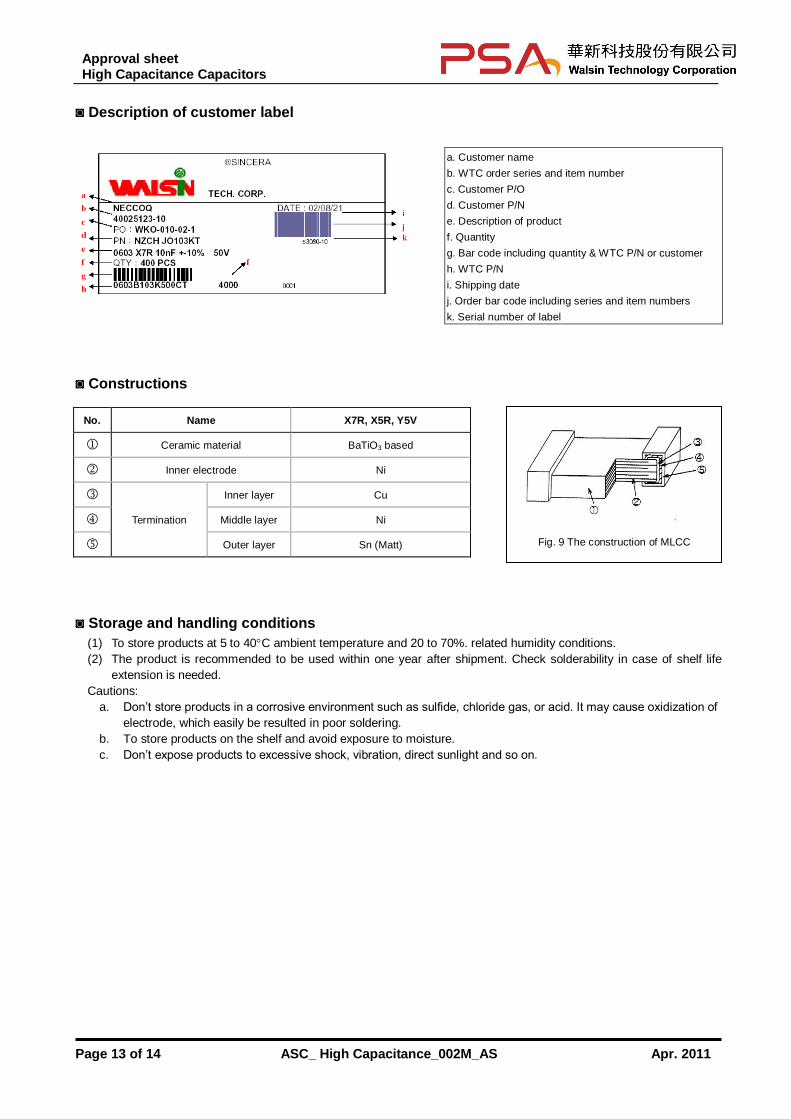
Description of customer label
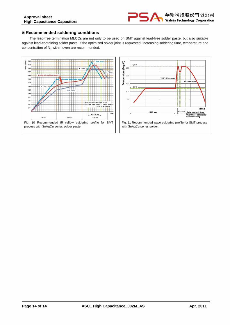
Constructions
Storage and handling conditions
(1) To store products at 5 to 40C ambient temperature and 20 to 70%. related humidity conditions.
(2) The product is recommended to be used within one year after shipment. Check solderability in case of shelf life
extension is needed.
Cautions:
a. Don’t store products in a corrosive environment such as sulfide, chloride gas, or acid. It may cause oxidization of
electrode, which easily be resulted in poor soldering.
b. To store products on the shelf and avoid exposure to moisture.
c. Don’t expose products to excessive shock, vibration, direct sunlight and so on.
No. Name X7R, X5R, Y5V
Ceramic material BaTiO3 based
Inner electrode Ni
Termination
Inner layer Cu
Middle layer Ni
Outer layer Sn (Matt)
Fig. 9 The construction of MLCC
a. Customer name
b. WTC order series and item number
c. Customer P/O
d. Customer P/N
e. Description of product
f. Quantity
g. Bar code including quantity & WTC P/N or customer
h. WTC P/N
i. Shipping date
j. Order bar code including series and item numbers
k. Serial number of label
Approval sheet High Capacitance Capacitors
Page 14 of 14 ASC_ High Capacitance_002M_AS Apr. 2011
Recommended soldering conditions
The lead-free termination MLCCs are not only to be used on SMT against lead-free solder paste, but also suitable
against lead-containing solder paste. If the optimized solder joint is requested, increasing soldering time, temperature and
concentration of N2 within oven are recommended.
Fig. 10 Recommended IR reflow soldering profile for SMT
process with SnAgCu series solder paste.
Fig. 11 Recommended wave soldering profile for SMT process
with SnAgCu series solder.
4/ sec max
Over 60sec at least by
natural cooling
4/ sec max
Over 60sec at least by
natural cooling


![4 J K - . 0 J ; 0 , K L 0 8 5 , J M - N O : 5 9 0 /, - , P ...l _ d m Y \ n d ] j ` a o \ Y ] ` \ d [ p o \ d m [ ] Y q [ c r s t p u [ ] a d Y i e o \ Y ] ` \ d [ t t s v p w x l](https://img.pdfslide.us/doc/110x75/5e752ae72f0d2b679431cf39/4-j-k-0-j-0-k-l-0-8-5-j-m-n-o-5-9-0-p-l-d-m-y-n-d-.jpg)