Embed Size (px)
Citation preview

For further information contact your local STMicroelectronics sales office.
October 2017 DocID031109 Rev 1 1/12
L9788
Multifunction IC for automotive engine management system
Data brief
Features AEC-Q100 qualified Engineered for ISO26262 compliant system 1 pre boost regulator and 1 pre buck regulator 1 linear 5 V regulator with 1 A output current 3 independent self-protection 5 V tracking
regulator with 150 mA output. 1 input voltage pin for monitor external
tracking. Coordinated soft start-up of all regulators 4 channels LS injector LS drivers 2 channels LS drivers for O2H load with current
sense 2 channels LS camshaft or solenoid drivers 5 channels LS relay drivers 2 channels LS LED drivers 3 channels LS/HS drivers with low battery
function for smart start
1 channel LS main relay driver (MRD) with internal diode for reverse battery protection
5 channels pre-drivers for external FET drivers - Predriver 1&3 configurable for O2H load with external Rshunt-on the source of Ext. N-Channel Mos
6 channels pre-drivers for internal or external igniter drivers
1 K-Line ISO9141/LIN 2.1 compliant Integrated charge-pump VRS-interface Watchdog Pin Wake-up Temperature sensor and monitoring Stop-counter with Wake-up Dual bandgap reference & oscillator Micro-second-channel MSC for differential
single ended mode SEO function CAN-FD with wake up by CAN function Package LQFP100 exposed pad
DescriptionThe L9788 is an integrated circuit designed for automotive engine management system.
L9788 is a device realized in ST BCD proprietary technology, able to provide the full set of power supplies and signal preprocessing peripherals needed to control a 4 cylinders internal combustion engine.
Table 1. Device summary Order code Package Packing
L9788 LQFP100 14x14x1.4 mm(Exposed pad down 7.6x7.6 mm)
Tube
L9788TR Tape & Reel
www.st.com

Contents L9788
2/12 DocID031109 Rev 1
Contents
1 Block diagram and pin description . . . . . . . . . . . . . . . . . . . . . . . . . . . . . 31.1 Block diagram . . . . . . . . . . . . . . . . . . . . . . . . . . . . . . . . . . . . . . . . . . . . . . . 3
1.2 Pin description . . . . . . . . . . . . . . . . . . . . . . . . . . . . . . . . . . . . . . . . . . . . . . 4
2 Package information . . . . . . . . . . . . . . . . . . . . . . . . . . . . . . . . . . . . . . . . . 82.1 LQFP100 (14x14x1.4 mm exp. pad down) package information . . . . . . . . 8
2.1.1 Exposed pad size option . . . . . . . . . . . . . . . . . . . . . . . . . . . . . . . . . . . . 10
3 Revision history . . . . . . . . . . . . . . . . . . . . . . . . . . . . . . . . . . . . . . . . . . . 11

DocID031109 Rev 1 3/12
L9788 Block diagram and pin description
12
1 Block diagram and pin description
1.1 Block diagram
Figure 1. Block diagram

Block diagram and pin description L9788
4/12 DocID031109 Rev 1
1.2 Pin description
Figure 2. Pin connection diagram (top view)
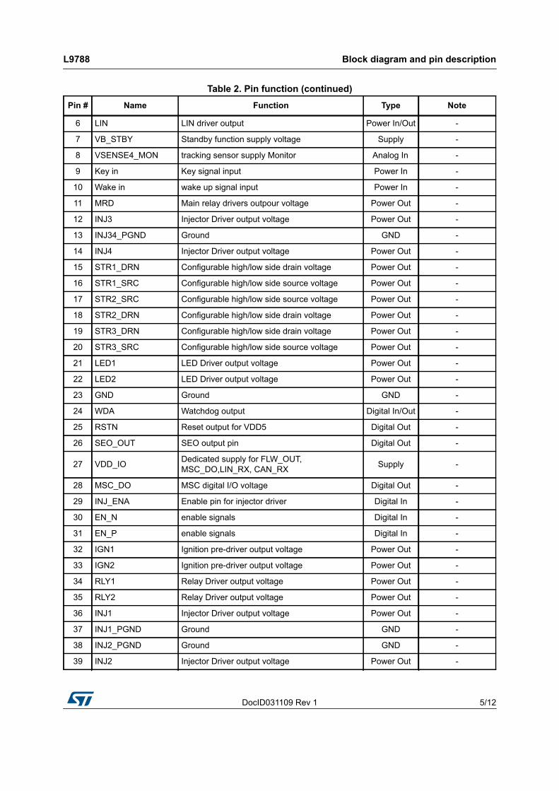
Table 2. Pin function Pin # Name Function Type Note
1 FLW_IN_P Flying wheel inputs voltage positive Power In -
2 FLW_IN_N Flying wheel inputs voltage negative Power In -
3 FLW_OUT Flying wheel output voltage Digital Out -
4 LIN_TX LIN data input Digital In -
5 LIN_RX LIN data output Digital Out -
DocID031109 Rev 1 5/12
L9788 Block diagram and pin description
12
6 LIN LIN driver output Power In/Out -
7 VB_STBY Standby function supply voltage Supply -
8 VSENSE4_MON tracking sensor supply Monitor Analog In -
9 Key in Key signal input Power In -
10 Wake in wake up signal input Power In -
11 MRD Main relay drivers outpour voltage Power Out -
12 INJ3 Injector Driver output voltage Power Out -
13 INJ34_PGND Ground GND -
14 INJ4 Injector Driver output voltage Power Out -
15 STR1_DRN Configurable high/low side drain voltage Power Out -
16 STR1_SRC Configurable high/low side source voltage Power Out -
17 STR2_SRC Configurable high/low side source voltage Power Out -
18 STR2_DRN Configurable high/low side drain voltage Power Out -
19 STR3_DRN Configurable high/low side drain voltage Power Out -
20 STR3_SRC Configurable high/low side source voltage Power Out -
21 LED1 LED Driver output voltage Power Out -
22 LED2 LED Driver output voltage Power Out -
23 GND Ground GND -
24 WDA Watchdog output Digital In/Out -
25 RSTN Reset output for VDD5 Digital Out -
26 SEO_OUT SEO output pin Digital Out -
27 VDD_IO Dedicated supply for FLW_OUT, MSC_DO,LIN_RX, CAN_RX Supply -
28 MSC_DO MSC digital I/O voltage Digital Out -
29 INJ_ENA Enable pin for injector driver Digital In -
30 EN_N enable signals Digital In -
31 EN_P enable signals Digital In -
32 IGN1 Ignition pre-driver output voltage Power Out -
33 IGN2 Ignition pre-driver output voltage Power Out -
34 RLY1 Relay Driver output voltage Power Out -
35 RLY2 Relay Driver output voltage Power Out -
36 INJ1 Injector Driver output voltage Power Out -
37 INJ1_PGND Ground GND -
38 INJ2_PGND Ground GND -
39 INJ2 Injector Driver output voltage Power Out -
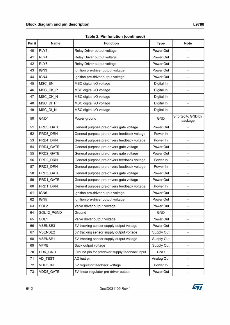
Table 2. Pin function (continued)Pin # Name Function Type Note
Block diagram and pin description L9788
6/12 DocID031109 Rev 1
40 RLY3 Relay Driver output voltage Power Out -
41 RLY4 Relay Driver output voltage Power Out -
42 RLY5 Relay Driver output voltage Power Out -
43 IGN3 Ignition pre-driver output voltage Power Out -
44 IGN4 Ignition pre-driver output voltage Power Out -
45 MSC_EN MSC digital I/O voltage Digital In -
46 MSC_CK_P MSC digital I/O voltage Digital In -
47 MSC_CK_N MSC digital I/O voltage Digital In -
48 MSC_DI_P MSC digital I/O voltage Digital In -
49 MSC_DI_N MSC digital I/O voltage Digital In -
50 GND1 Power ground GND Shorted to GND by package
51 PRD5_GATE General purpose pre-drivers gate voltage Power Out -
52 PRD5_DRN General purpose pre-drivers feedback voltage Power In -
53 PRD4_DRN General purpose pre-drivers feedback voltage Power In -
54 PRD4_GATE General purpose pre-drivers gate voltage Power Out -
55 PRD2_GATE General purpose pre-drivers gate voltage Power Out -
56 PRD2_DRN General purpose pre-drivers feedback voltage Power In -
57 PRD3_DRN General purpose pre-drivers feedback voltage Power In -
58 PRD3_GATE General purpose pre-drivers gate voltage Power Out -
59 PRD1_GATE General purpose pre-drivers gate voltage Power Out -
60 PRD1_DRN General purpose pre-drivers feedback voltage Power In -
61 IGN6 Ignition pre-driver output voltage Power Out -
62 IGN5 Ignition pre-driver output voltage Power Out -
63 SOL2 Valve driver output voltage Power Out -
64 SOL12_PGND Ground GND -
65 SOL1 Valve driver output voltage Power Out -
66 VSENSE3 5V tracking sensor supply output voltage Power Out -
67 VSENSE2 5V tracking sensor supply output voltage Supply Out -
68 VSENSE1 5V tracking sensor supply output voltage Supply Out -
69 VPRE Buck output voltage Supply Out -
70 PDR_GND Ground pin for predriver supply feedback input GND -
71 AD_TEST AD test pin Analog Out -
72 VDD5_IN 5V regulator feedback voltage Power In -
73 VDD5_GATE 5V linear regulator pre-driver output Power Out -
Table 2. Pin function (continued)Pin # Name Function Type Note

DocID031109 Rev 1 7/12
L9788 Block diagram and pin description
12
74 RSTC Reset output for VDDIO supply Digital Out -
75 GND Ground GND -
76 Boost_G Boost LS gate voltage Power Out -
77 VBAT_Sense Battery supply voltage Supply In -
78 VB_IN Battery supply voltage Supply In -
79 CP Charge pump Power Out -
80 Buck_C_BST Bootstrap capacitor pin Power Out -
81 Buck_SW Buck switching pin Power Out -
82 VB_IN_SW BUCK supply voltage Power In -
83 CURR_Sense_O2H2 O2heater drivers output current value Analog Out -
84 O2H2_PGNDB Ground GND -
85 O2H2B O2H2B Driver output voltage Power Out -
86 O2H2A O2H2A Driver output voltage Power Out -
87 O2H2_PGNDA Ground GND -
88 O2H1_PGNDB Ground GND -
89 O2H1B O2H1BDriver output voltage Power Out -
90 O2H1A O2H1A Driver output voltage Power Out -
91 O2H1_PGNDA Ground GND -
92 VDD_CAN CAN Supply 5 V Supply In -
93 CURR_Sense_O2H1 O2heater drivers output current value Analog Out -
94 CANH CANH output Power In/Out -
95 CANL CANL output Power In/Out -
96 CAN_RX CAN RX data output Digital In/Out -
97 GND Ground GND -
98 CAN_TX CAN TX data input Digital In -
99 VB_CAN CAN enable signal Supply In -
100 GND_CAN Ground CAN GND -
Table 2. Pin function (continued)Pin # Name Function Type Note
Package information L9788
8/12 DocID031109 Rev 1
2 Package information
In order to meet environmental requirements, ST offers these devices in different grades of ECOPACK® packages, depending on their level of environmental compliance. ECOPACK® specifications, grade definitions and product status are available at: www.st.com. ECOPACK® is an ST trademark.
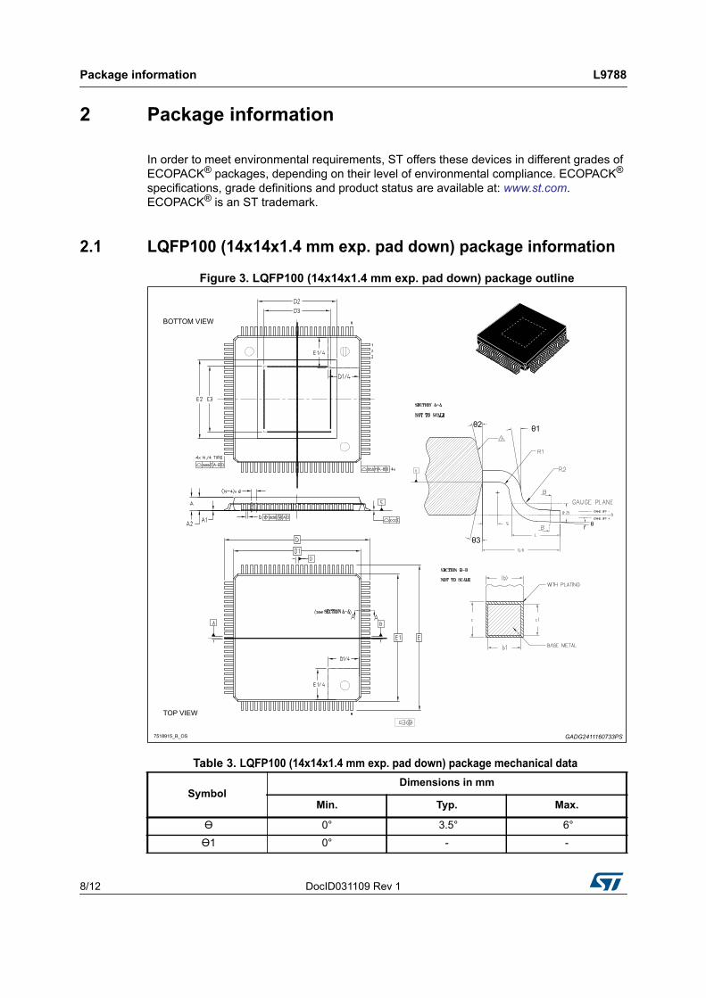
2.1 LQFP100 (14x14x1.4 mm exp. pad down) package information
Figure 3. LQFP100 (14x14x1.4 mm exp. pad down) package outline
Table 3. LQFP100 (14x14x1.4 mm exp. pad down) package mechanical data
SymbolDimensions in mm
Min. Typ. Max.
Ө 0° 3.5° 6°
Ө1 0° - -

DocID031109 Rev 1 9/12
L9788 Package information
12
Ө2 11° 12° 13°
Ө3 11° 12° 13°
A - 1.40 1.60
A1 0.05 - 0.15
A2 1.35 1.40 1.45
b 0.17 0.22 0.27
b1 0.17 0.20 0.23
c 0.09 - 0.20
c1 0.09 - 0.16
D 16.00 BSC
D1(1) (2) 16.00 BSC
D2 See VARIATIONS D3 See VARIATIONS e 0.50 BSC
E 16.00 BSC
E1(1) (2) 14.00 BSC
E2 See VARIATIONS E3 See VARIATIONS L 0.45 0.60 0.75
L1 1.00 REF
N 100
R1 0.08 - -
R2 0.08 - 0.20
S 0.20 - -
Tolerance of form and positionaaa 0.20
bbb 0.20
ccc 0.08
ddd 0.08
VARIATIONSPad option 3.5x3.5 (T3)(3)
D2 - - 4.61
E2 - - 4.61
D3 2.30 - -
E3 2.30 - -
Table 3. LQFP100 (14x14x1.4 mm exp. pad down) package mechanical data (continued)
SymbolDimensions in mm
Min. Typ. Max.

Package information L9788
10/12 DocID031109 Rev 1
2.1.1 Exposed pad size optionL9788 uses the exposed pad option 7.6 x 7.6 mm.
Pad option 4.5X4.5 (T3)(3)
D2 - - 4.71
E2 - - 4.71
D3 3.30 - -
E3 3.30 - -
Pad option 6.0X6.0 (T3)(3)
D2 - - 6.21
E2 - - 6.21
D3 4.96 - -
E3 4.96 - -
Pad option 7.6X7.6 (T3)(3)
D2 - - 7.95
E2 - - 7.95
D3 6.34 - -
E3 6.34 - -
1. Dimensions D1 and E1 do not include mold flash or protrusions.Allowable mold flash or protrusion is “0.25 mm” per side.
2. The Top package body size may be smaller than the bottom package size by much as 0.15 mm.
3. Number, dimensions and position of shown groves are for reference only:
Table 3. LQFP100 (14x14x1.4 mm exp. pad down) package mechanical data (continued)
SymbolDimensions in mm
Min. Typ. Max.

DocID031109 Rev 1 11/12
L9788 Revision history
12
3 Revision history
Table 4. Document revision historyDate Revision Changes
06-Oct-2017 1 Initial release.

L9788
12/12 DocID031109 Rev 1
IMPORTANT NOTICE – PLEASE READ CAREFULLY
STMicroelectronics NV and its subsidiaries (“ST”) reserve the right to make changes, corrections, enhancements, modifications, and improvements to ST products and/or to this document at any time without notice. Purchasers should obtain the latest relevant information on ST products before placing orders. ST products are sold pursuant to ST’s terms and conditions of sale in place at the time of order acknowledgement.
Purchasers are solely responsible for the choice, selection, and use of ST products and ST assumes no liability for application assistance or the design of Purchasers’ products.
No license, express or implied, to any intellectual property right is granted by ST herein.
Resale of ST products with provisions different from the information set forth herein shall void any warranty granted by ST for such product.
ST and the ST logo are trademarks of ST. All other product or service names are the property of their respective owners.
Information in this document supersedes and replaces information previously supplied in any prior versions of this document.
© 2017 STMicroelectronics – All rights reserved