Embed Size (px)
Citation preview
July 2009
Agilent EEsof EDA Overview
New Capabilities in ADS 2011:
Multi-Technology Design Flow
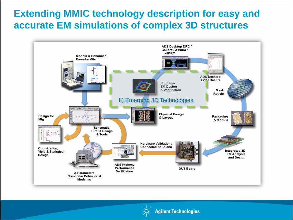
Extending MMIC technology
description for easy and accurate
EM simulations of complex 3D
structures
MMIC Design
Symposium
Agilent EEsof EDA
Ingo Nickeleit,
Application Engineer
February 2012
http://www.agilent.com/find/eesof
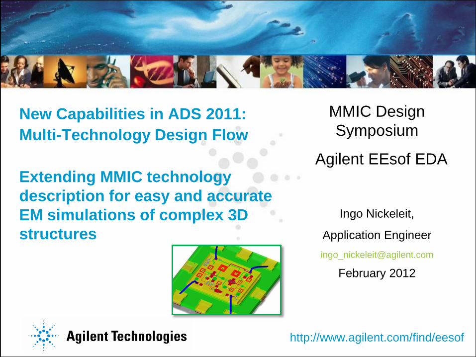
Agenda – Complete MMIC/Module Design Flow
I) Multi-Technology
III) Foundry Updates
Integrated EM &
Package Design
II) Emerging 3D Technologies
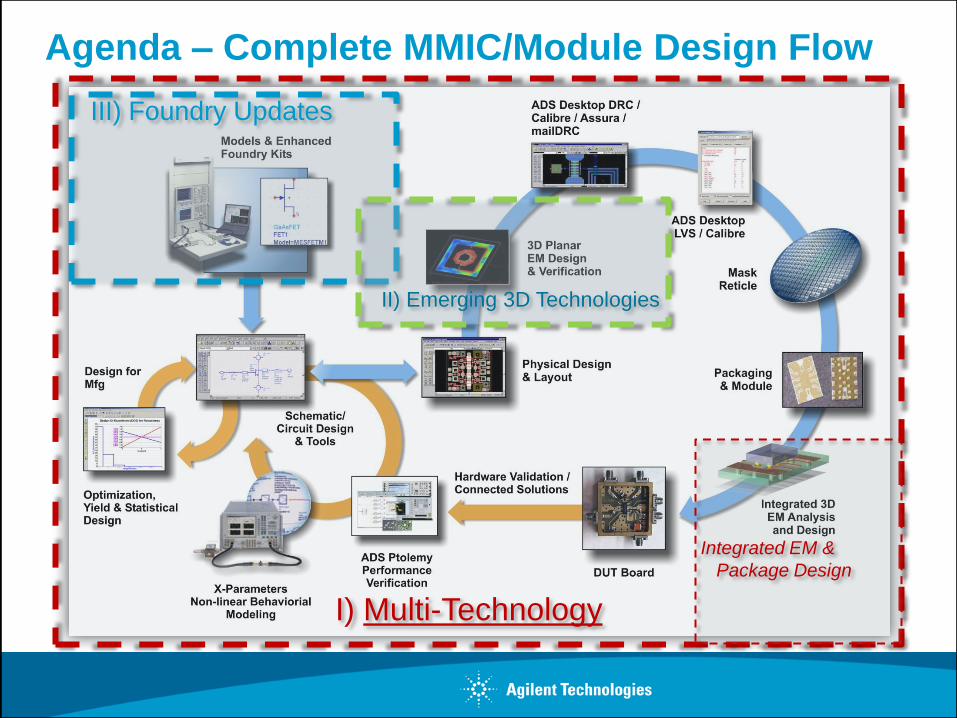
Technology Foundry Scope
MMIC
(GaAs / GaN)
• Front-to-Back PDK creation
• DRC rule deck
• EM substrate
• MMIC tool bar
• Training
• Joint webinar and customer visit
RFIC
(SiGe/CMOS)
• Front-end PDK creation
• Momentum module support
• Increasing back-end support (for SiGe)
• GoldenGate qualification
• EM Qualification
Foundry Engagement – A Major Focus Area
www.agilent.com/find/eesof-foundries
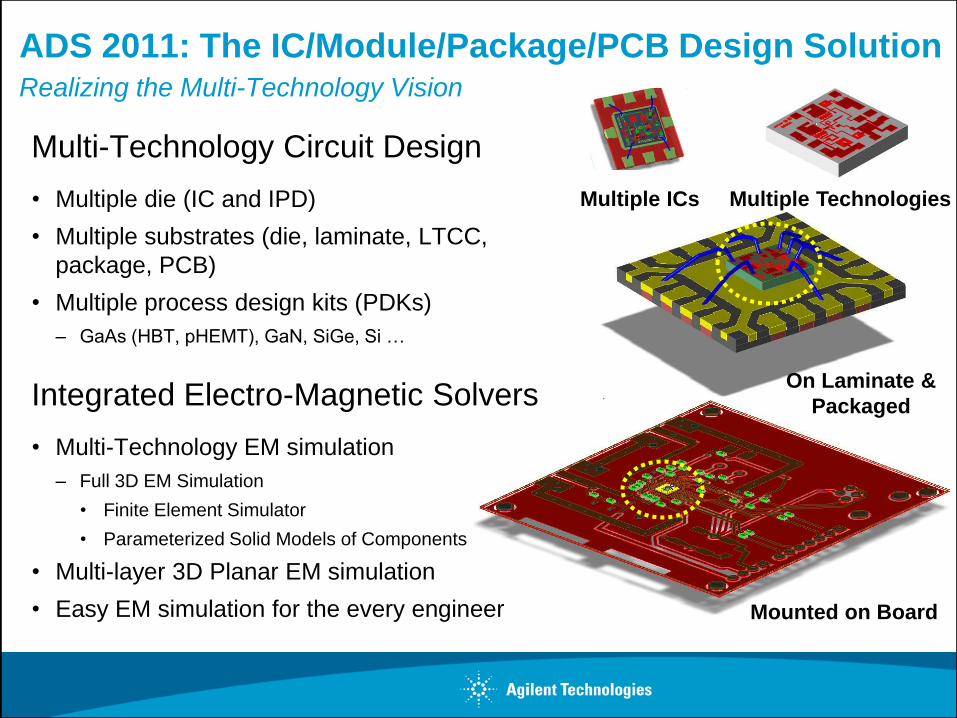
ADS 2011: The IC/Module/Package/PCB Design Solution Realizing the Multi-Technology Vision
Multi-Technology Circuit Design
• Multiple die (IC and IPD)
• Multiple substrates (die, laminate, LTCC,
package, PCB)
• Multiple process design kits (PDKs)
– GaAs (HBT, pHEMT), GaN, SiGe, Si …
Integrated Electro-Magnetic Solvers
• Multi-Technology EM simulation
– Full 3D EM Simulation
• Finite Element Simulator
• Parameterized Solid Models of Components
• Multi-layer 3D Planar EM simulation
• Easy EM simulation for the every engineer Mounted on Board
Multiple ICs Multiple Technologies
On Laminate &
Packaged
Designing Across Multiple Technologies
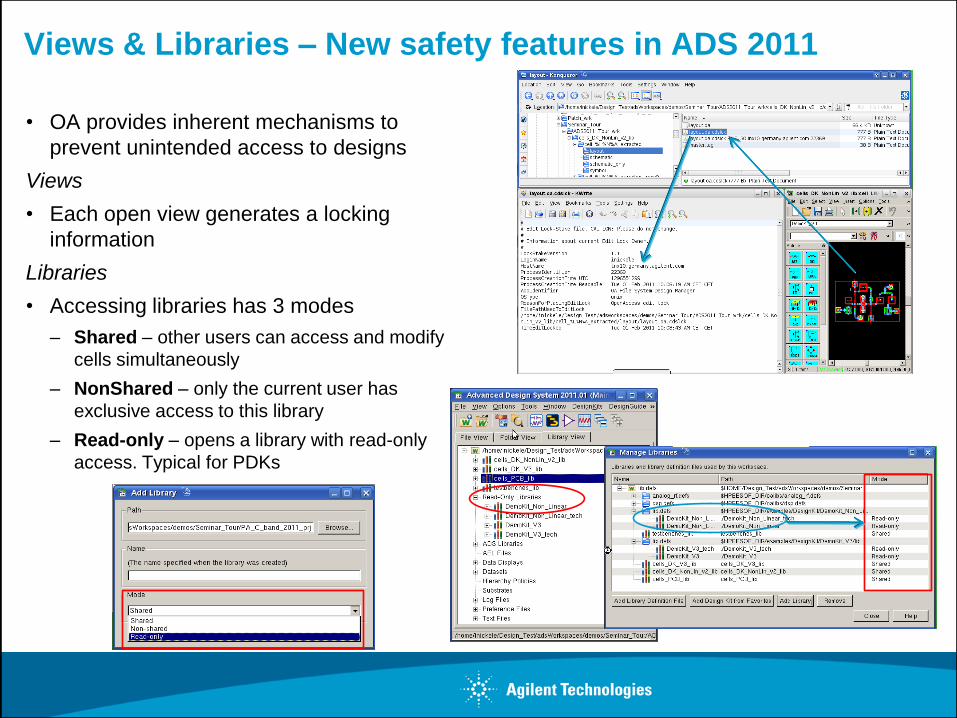
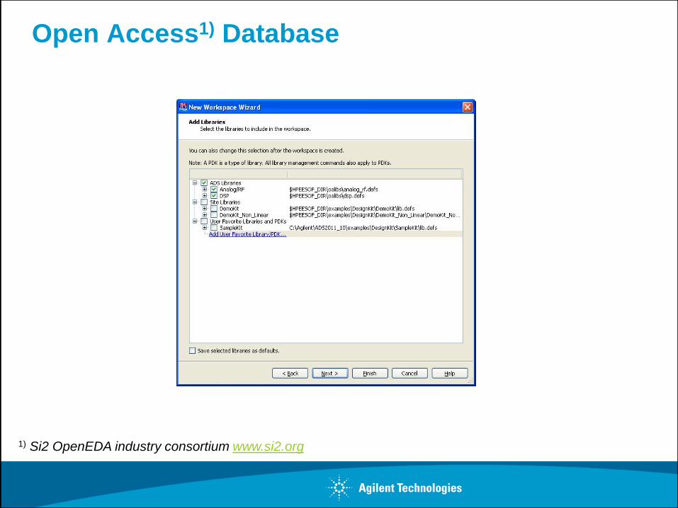
Views & Libraries – New safety features in ADS 2011
• OA provides inherent mechanisms to
prevent unintended access to designs
Views
• Each open view generates a locking
information
Libraries
• Accessing libraries has 3 modes
– Shared – other users can access and modify
cells simultaneously
– NonShared – only the current user has
exclusive access to this library
– Read-only – opens a library with read-only
access. Typical for PDKs
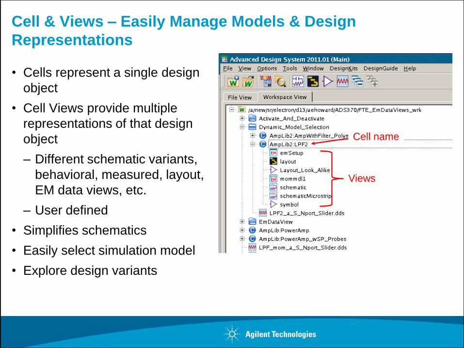
Cell & Views – Easily Manage Models & Design
Representations
• Cells represent a single design
object
• Cell Views provide multiple
representations of that design
object
– Different schematic variants,
behavioral, measured, layout,
EM data views, etc.
– User defined
• Simplifies schematics
• Easily select simulation model
• Explore design variants
Cell name
Views
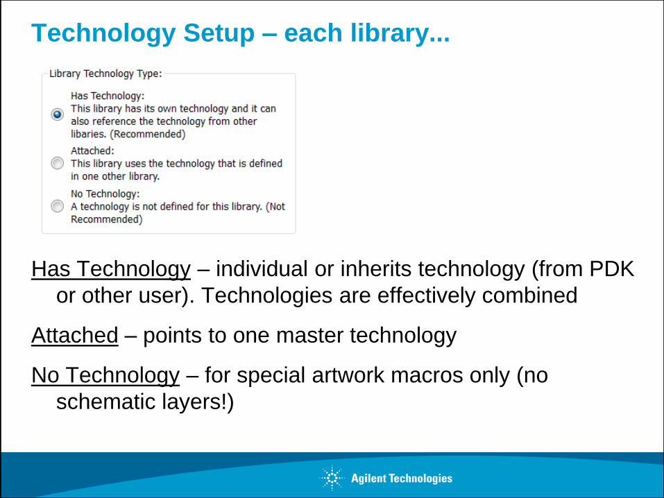
Technology Setup – each library...
Has Technology – individual or inherits technology (from PDK
or other user). Technologies are effectively combined
Attached – points to one master technology
No Technology – for special artwork macros only (no
schematic layers!)
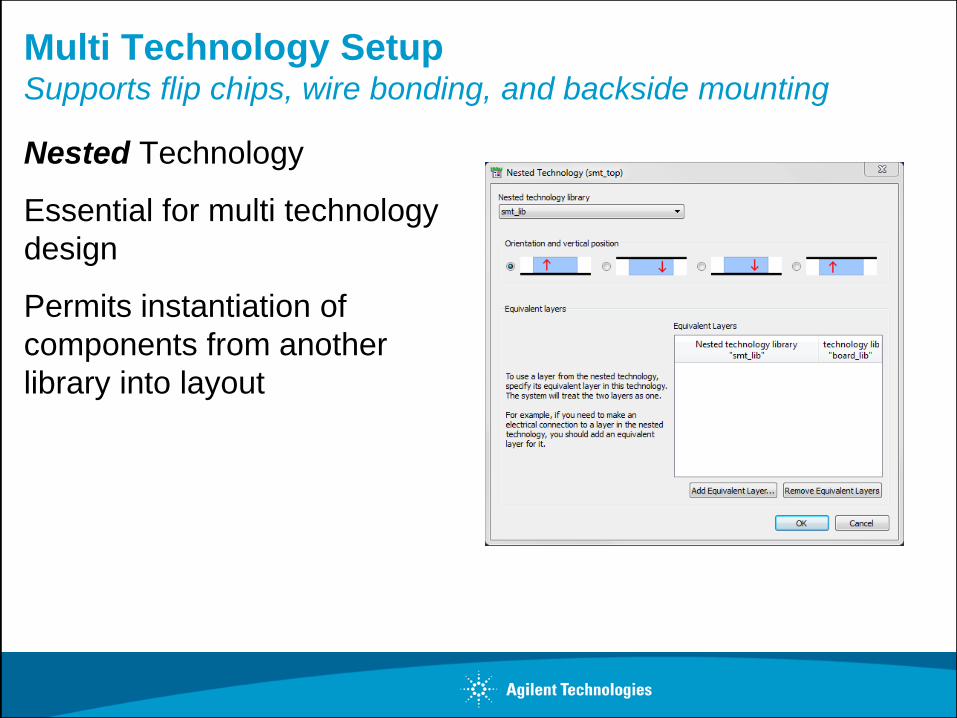
Multi Technology Setup Supports flip chips, wire bonding, and backside mounting
Nested Technology
Essential for multi technology
design
Permits instantiation of
components from another
library into layout
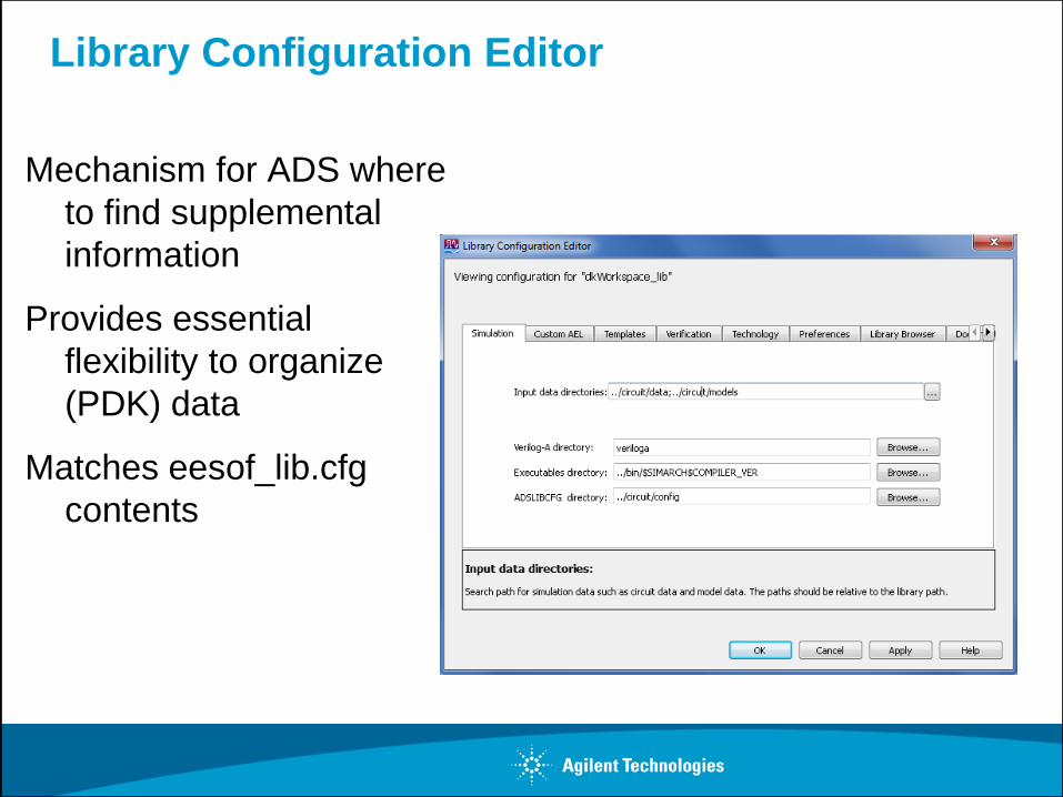
Library Configuration Editor
Mechanism for ADS where
to find supplemental
information
Provides essential
flexibility to organize
(PDK) data
Matches eesof_lib.cfg
contents
Multi-technology EM
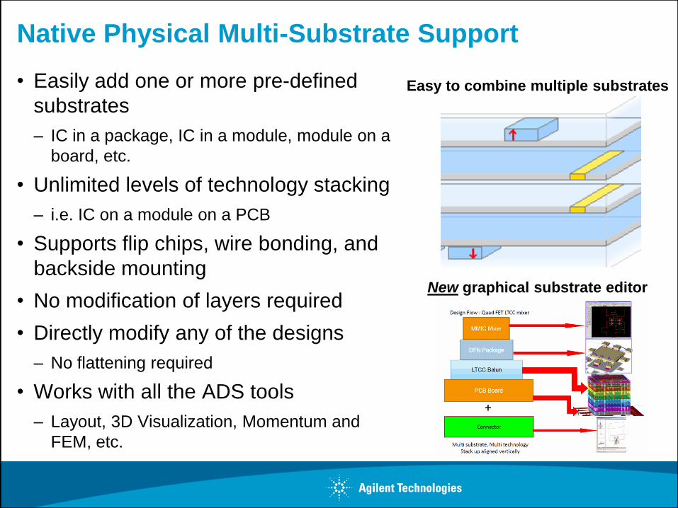
Native Physical Multi-Substrate Support
• Easily add one or more pre-defined
substrates
– IC in a package, IC in a module, module on a
board, etc.
• Unlimited levels of technology stacking
– i.e. IC on a module on a PCB
• Supports flip chips, wire bonding, and
backside mounting
• No modification of layers required
• Directly modify any of the designs
– No flattening required
• Works with all the ADS tools
– Layout, 3D Visualization, Momentum and
FEM, etc.
Easy to combine multiple substrates
New graphical substrate editor
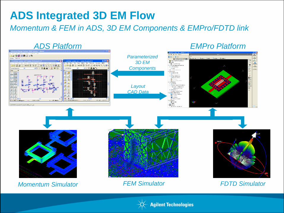
ADS Integrated 3D EM Flow Momentum & FEM in ADS, 3D EM Components & EMPro/FDTD link
EMPro Platform ADS Platform
FDTD Simulator FEM Simulator Momentum Simulator
Parameterized
3D EM
Components
Layout
CAD Data
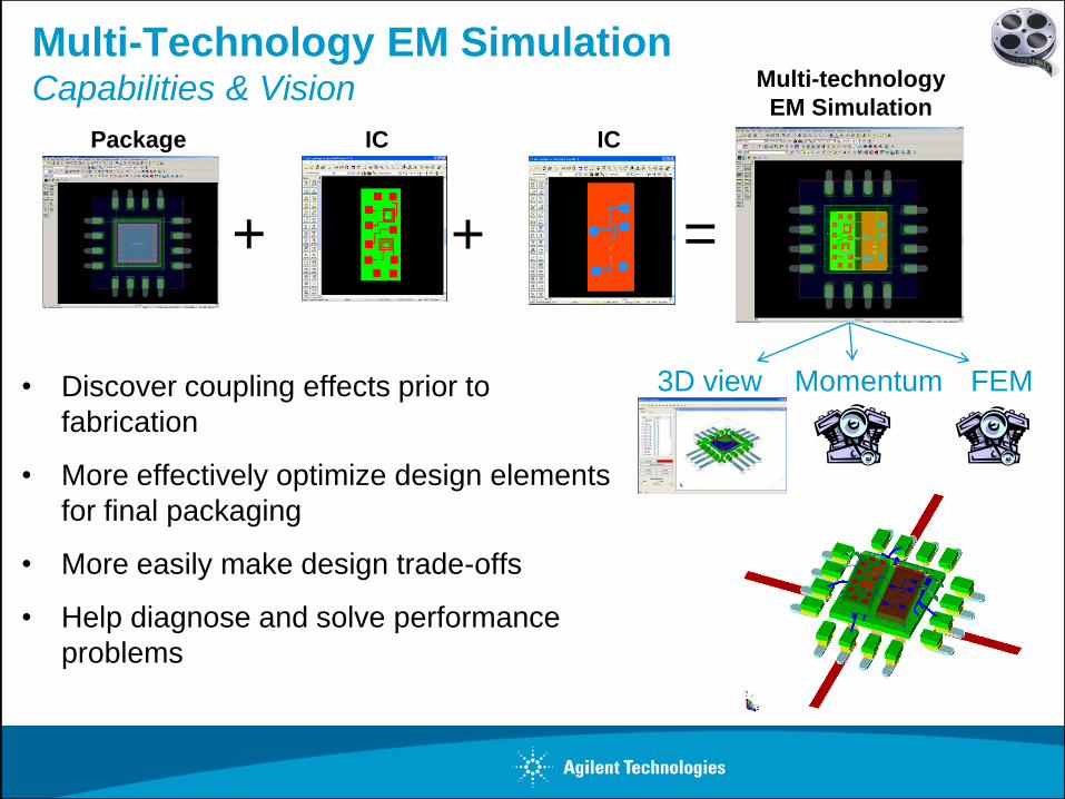
Multi-Technology EM Simulation Capabilities & Vision
• Discover coupling effects prior to
fabrication
• More effectively optimize design elements
for final packaging
• More easily make design trade-offs
• Help diagnose and solve performance
problems
+ =
3D view FEM Momentum
+
Package IC IC
Multi-technology
EM Simulation
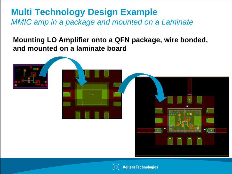
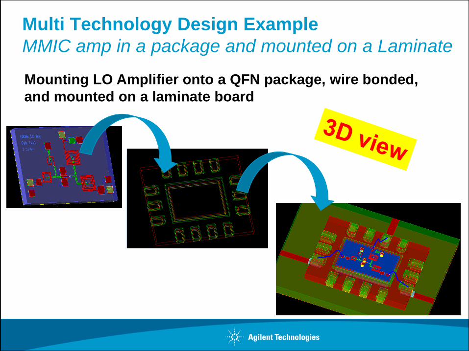
Multi Technology Design Example MMIC amp in a package and mounted on a Laminate
Mounting LO Amplifier onto a QFN package, wire bonded,
and mounted on a laminate board
Multi Technology Design Example
MMIC amp in a package and mounted on a Laminate
Mounting LO Amplifier onto a QFN package, wire bonded,
and mounted on a laminate board
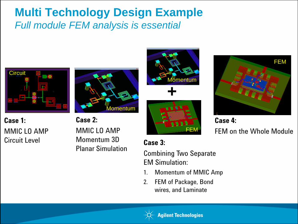
Multi Technology Design Example Full module FEM analysis is essential
Case 1:
MMIC LO AMP
Circuit Level
Case 2:
MMIC LO AMP
Momentum 3D
Planar Simulation
+
Case 3:
Combining Two Separate
EM Simulation:
1. Momentum of MMIC Amp
2. FEM of Package, Bond
wires, and Laminate
Case 4:
FEM on the Whole Module
Momentum
FEM
FEM
Momentum
Circuit
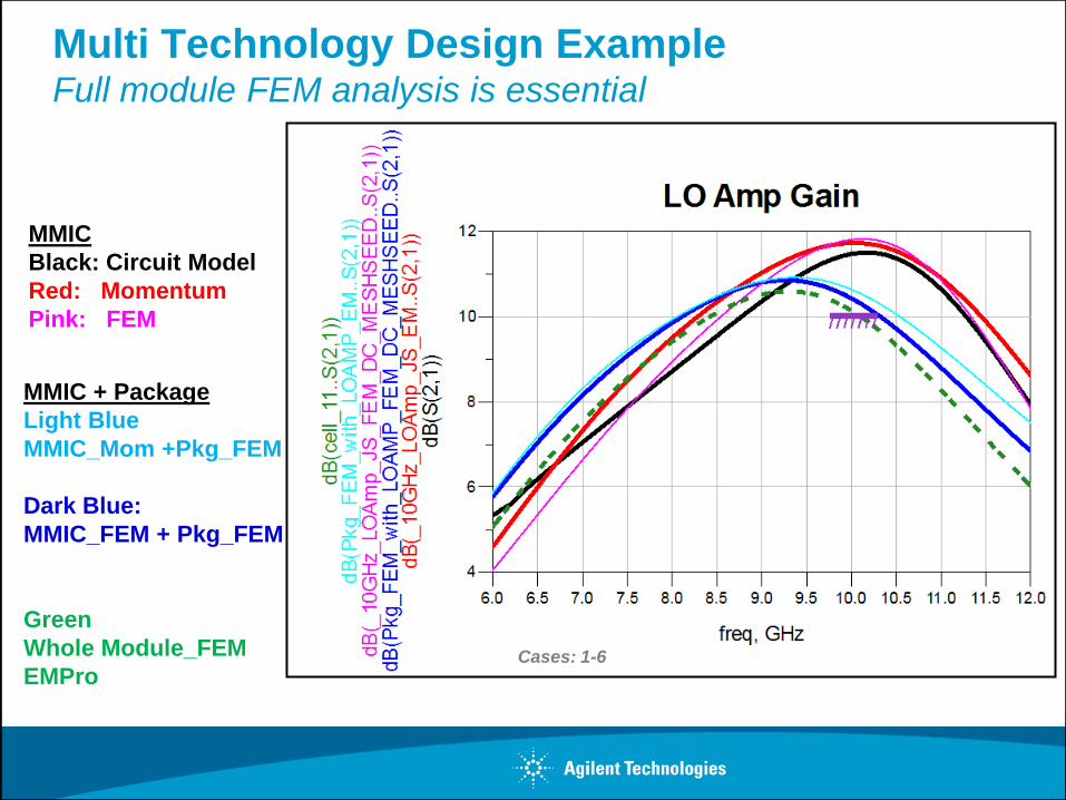
Multi Technology Design Example Full module FEM analysis is essential
Cases: 1-6
MMIC
Black: Circuit Model
Red: Momentum
Pink: FEM
MMIC + Package
Light Blue
MMIC_Mom +Pkg_FEM
Dark Blue:
MMIC_FEM + Pkg_FEM
Green
Whole Module_FEM
EMPro
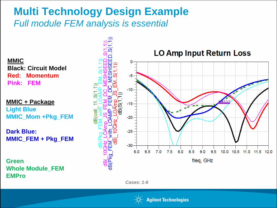
Multi Technology Design Example Full module FEM analysis is essential
Cases: 1-6
MMIC
Black: Circuit Model
Red: Momentum
Pink: FEM
MMIC + Package
Light Blue
MMIC_Mom +Pkg_FEM
Dark Blue:
MMIC_FEM + Pkg_FEM
Green
Whole Module_FEM
EMPro
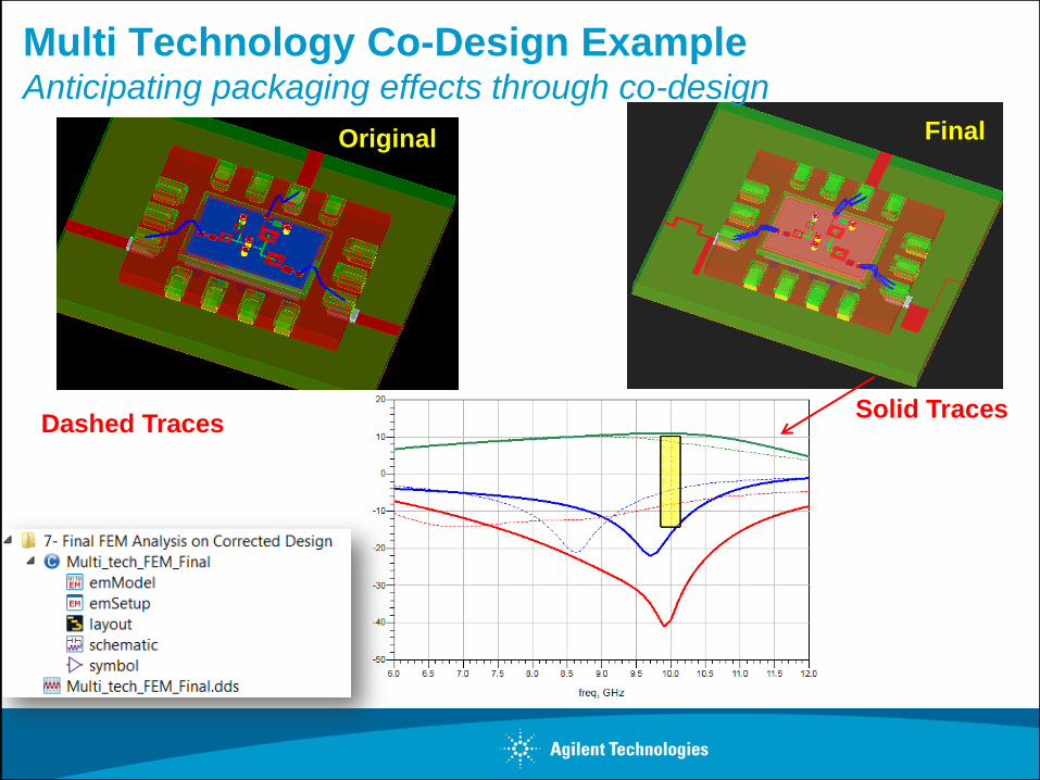
Multi Technology Co-Design Example Anticipating packaging effects through co-design
Solid Traces Dashed Traces
Original Final
Improved RF Circuit Design and Simulation
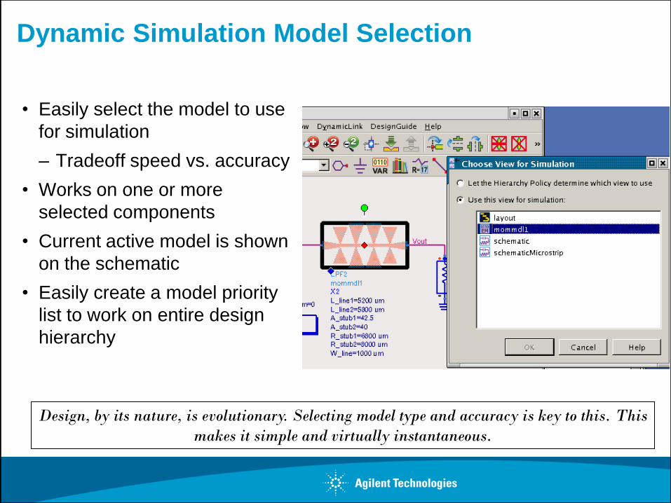
Dynamic Simulation Model Selection
Design, by its nature, is evolutionary. Selecting model type and accuracy is key to this. This
makes it simple and virtually instantaneous.
• Easily select the model to use
for simulation
– Tradeoff speed vs. accuracy
• Works on one or more
selected components
• Current active model is shown
on the schematic
• Easily create a model priority
list to work on entire design
hierarchy
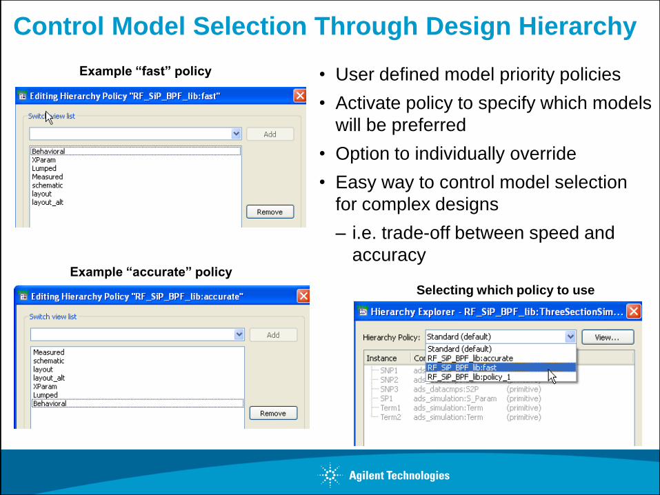
Control Model Selection Through Design Hierarchy
• User defined model priority policies
• Activate policy to specify which models
will be preferred
• Option to individually override
• Easy way to control model selection
for complex designs
– i.e. trade-off between speed and
accuracy
Example “fast” policy
Example “accurate” policy
Selecting which policy to use
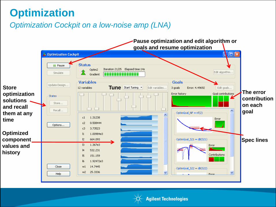
Optimization Optimization Cockpit on a low-noise amp (LNA)
Spec lines
Pause optimization and edit algorithm or
goals and resume optimization
Optimized
component
values and
history
The error
contribution
on each
goal
Store
optimization
solutions
and recall
them at any
time
Tune
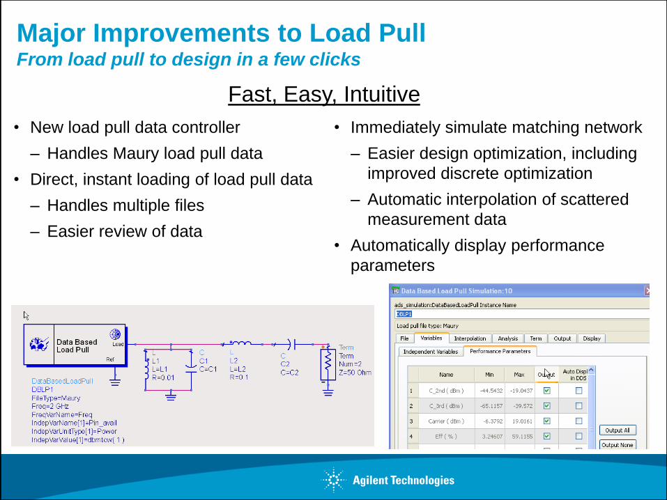
Major Improvements to Load Pull From load pull to design in a few clicks
• New load pull data controller
– Handles Maury load pull data
• Direct, instant loading of load pull data
– Handles multiple files
– Easier review of data
• Immediately simulate matching network
– Easier design optimization, including
improved discrete optimization
– Automatic interpolation of scattered
measurement data
• Automatically display performance
parameters
Fast, Easy, Intuitive
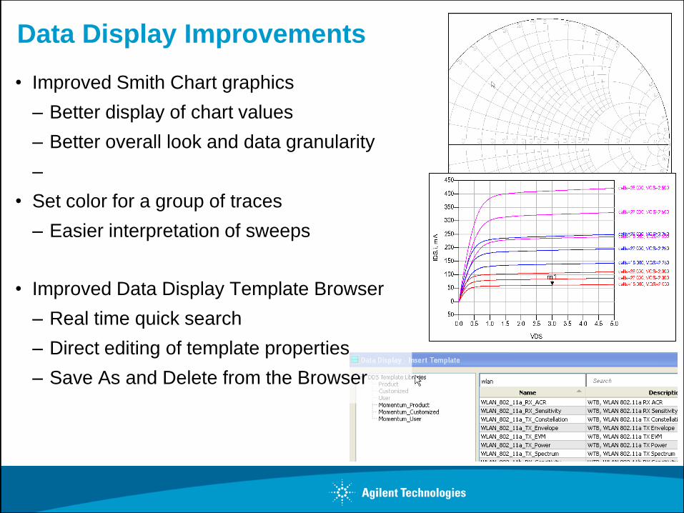
Data Display Improvements
• Improved Smith Chart graphics
– Better display of chart values
– Better overall look and data granularity
–
• Set color for a group of traces
– Easier interpretation of sweeps
• Improved Data Display Template Browser
– Real time quick search
– Direct editing of template properties
– Save As and Delete from the Browser
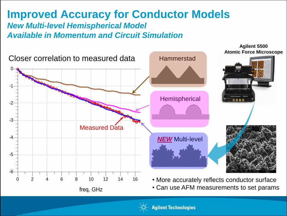
Improved Accuracy for Conductor Models New Multi-level Hemispherical Model
Available in Momentum and Circuit Simulation
Closer correlation to measured data Hammerstad
The original hemispherical model
Hemispherical
NEW Multi-level
2 4 6 8 10 12 14 16 180 20
-5
-4
-3
-2
-1
-6
0
freq, GHz
dB
(meas_2000m
il_ro
4350b..
S(2
,1))
dB
(yunhui_
bb4_hfc
orr
0..
S(2
,1))
dB
(S(2
,1))
dB
(yunhui_
bb4_hfc
orr
1_9..
S(2
,1))
SEM photograph of rough copper at
5000x magnification at a 30 degree angle.
Courtesy of Steven Hall et al. 2007
Measured Data
Agilent 5500
Atomic Force Microscope
• More accurately reflects conductor surface
• Can use AFM measurements to set params
MMIC Backend Design Process
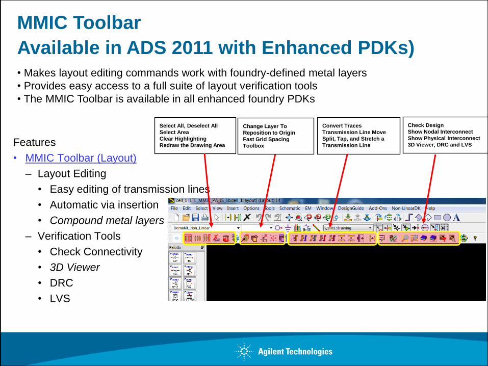
MMIC Toolbar
Available in ADS 2011 with Enhanced PDKs)
Features
• MMIC Toolbar (Layout)
– Layout Editing
• Easy editing of transmission lines
• Automatic via insertion
• Compound metal layers
– Verification Tools
• Check Connectivity
• 3D Viewer
• DRC
• LVS
• Makes layout editing commands work with foundry-defined metal layers
• Provides easy access to a full suite of layout verification tools
• The MMIC Toolbar is available in all enhanced foundry PDKs
Select All, Deselect All
Select Area
Clear Highlighting
Redraw the Drawing Area
Convert Traces
Transmission Line Move
Split, Tap, and Stretch a
Transmission Line
Change Layer To
Reposition to Origin
Fast Grid Spacing
Toolbox
Check Design
Show Nodal Interconnect
Show Physical Interconnect
3D Viewer, DRC and LVS
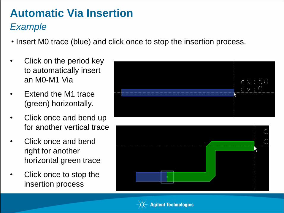
Automatic Via Insertion
Example
• Insert M0 trace (blue) and click once to stop the insertion process.
• Click on the period key
to automatically insert
an M0-M1 Via
• Extend the M1 trace
(green) horizontally.
• Click once and bend up
for another vertical trace
• Click once and bend
right for another
horizontal green trace
• Click once to stop the
insertion process
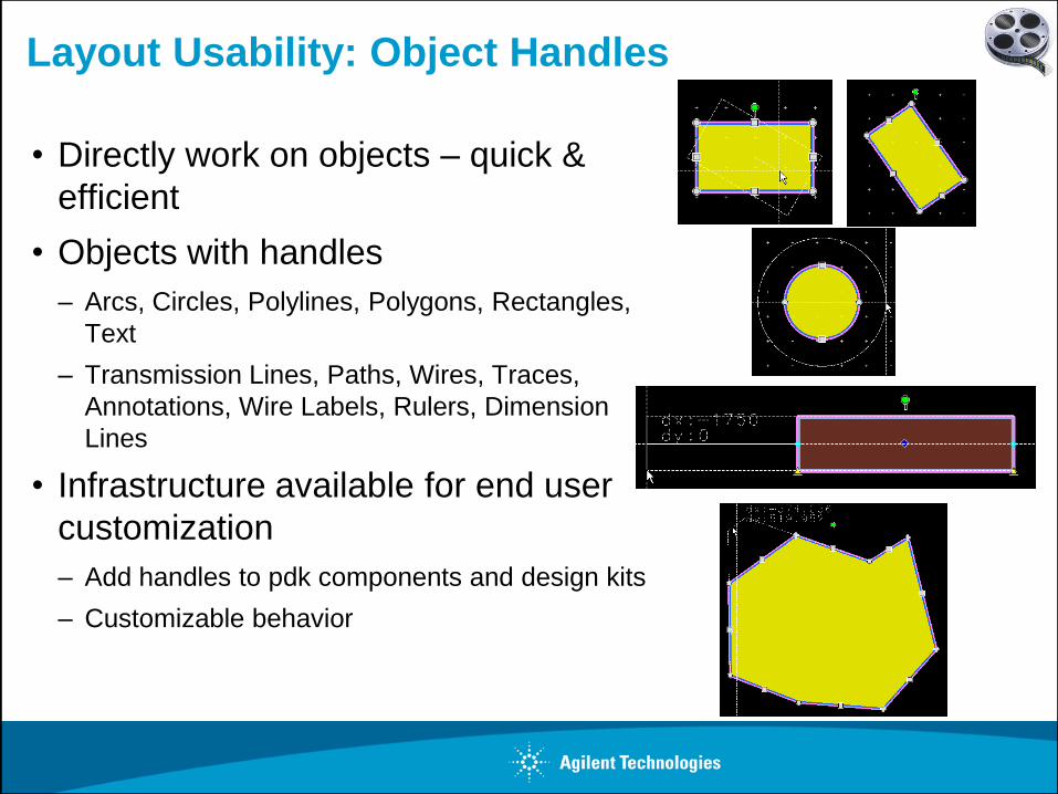
Layout Usability: Object Handles
• Directly work on objects – quick &
efficient
• Objects with handles
– Arcs, Circles, Polylines, Polygons, Rectangles,
Text
– Transmission Lines, Paths, Wires, Traces,
Annotations, Wire Labels, Rulers, Dimension
Lines
• Infrastructure available for end user
customization
– Add handles to pdk components and design kits
– Customizable behavior
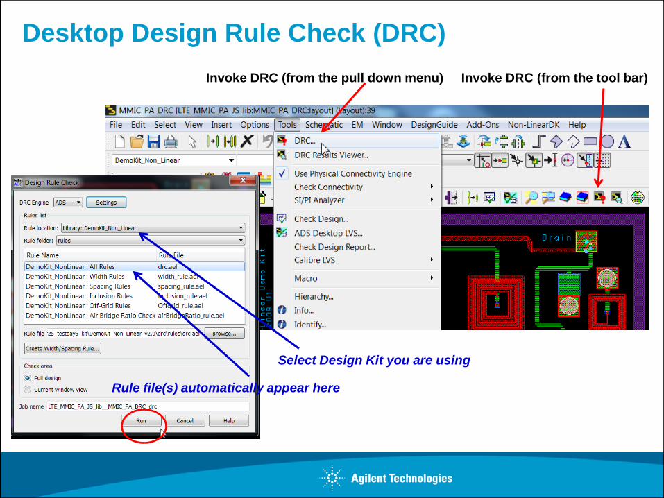
Desktop Design Rule Check (DRC)
Invoke DRC (from the pull down menu) Invoke DRC (from the tool bar)
Select Design Kit you are using
Rule file(s) automatically appear here
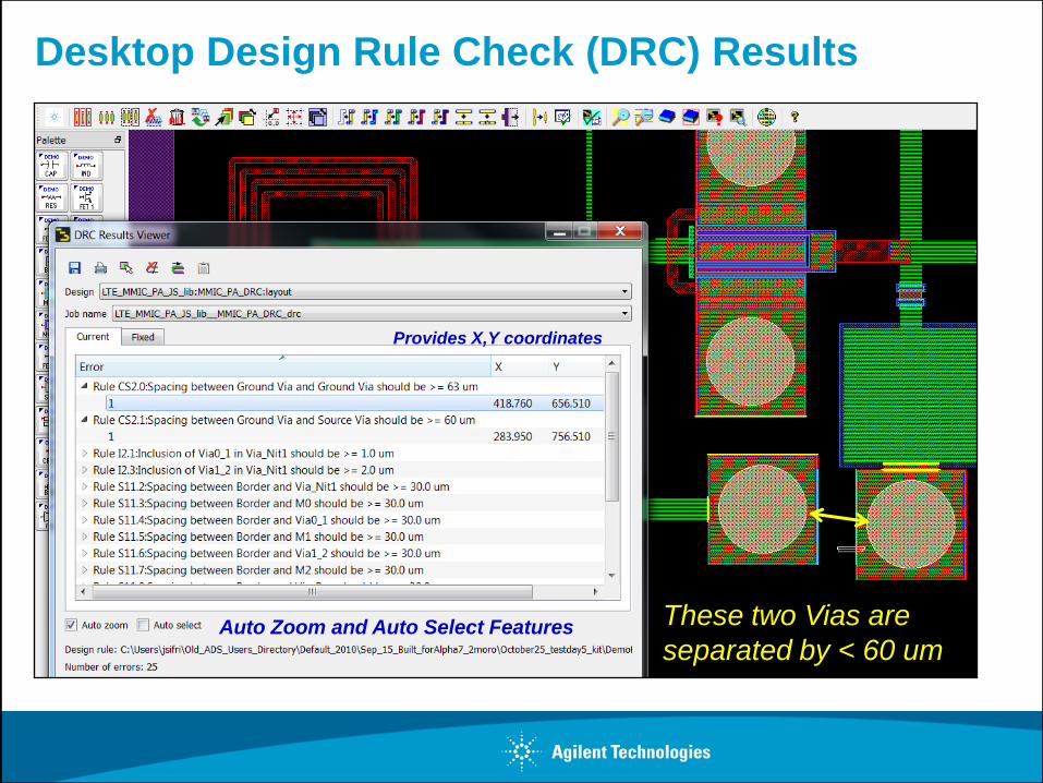
Desktop Design Rule Check (DRC) Results
These two Vias are
separated by < 60 um Auto Zoom and Auto Select Features
Provides X,Y coordinates
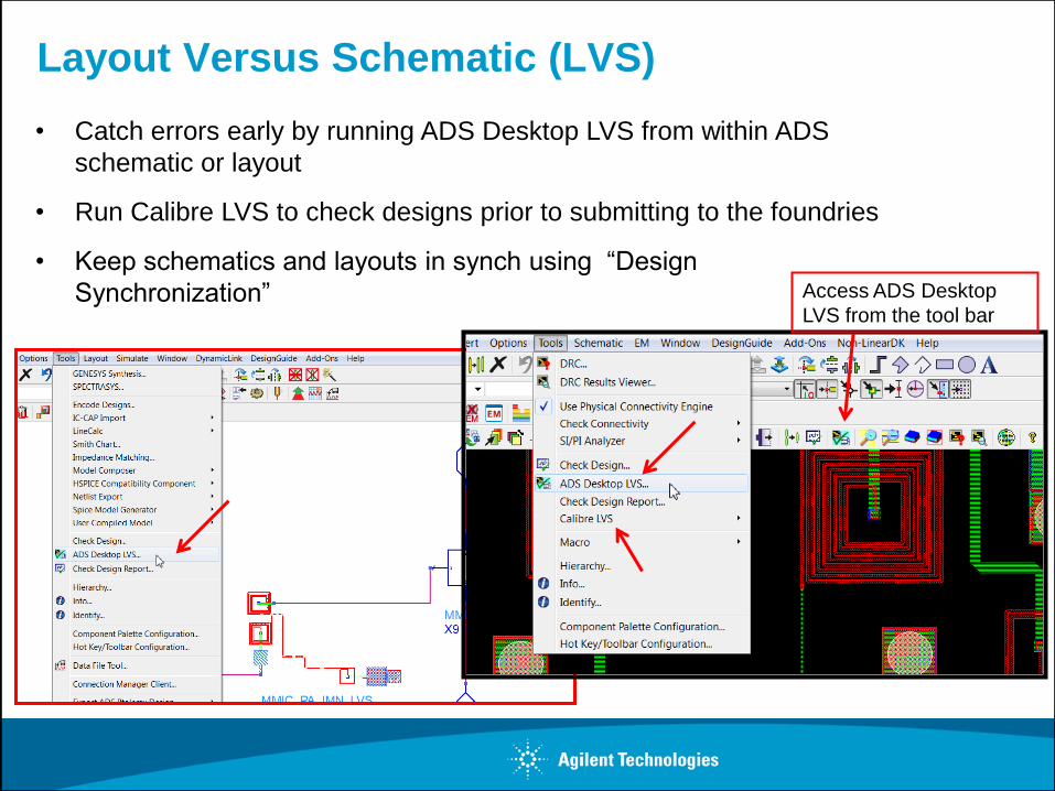
Layout Versus Schematic (LVS)
• Catch errors early by running ADS Desktop LVS from within ADS
schematic or layout
• Run Calibre LVS to check designs prior to submitting to the foundries
• Keep schematics and layouts in synch using “Design
Synchronization” Access ADS Desktop
LVS from the tool bar
Making EM Simulation
Part of Everyone’s Design Flow
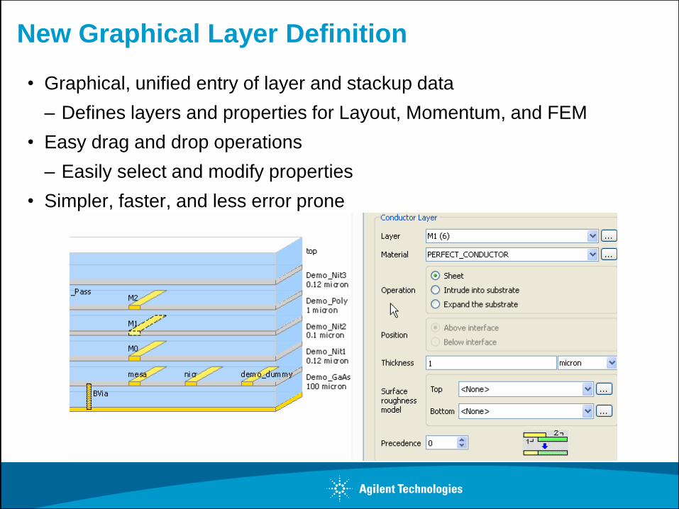
New Graphical Layer Definition
• Graphical, unified entry of layer and stackup data
– Defines layers and properties for Layout, Momentum, and FEM
• Easy drag and drop operations
– Easily select and modify properties
• Simpler, faster, and less error prone
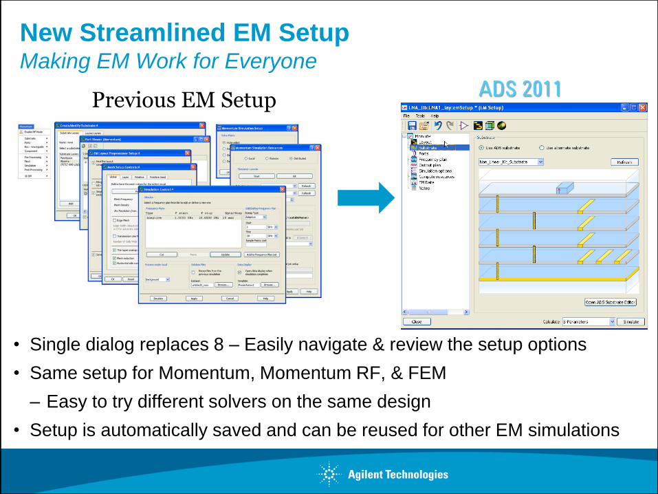
New Streamlined EM Setup Making EM Work for Everyone
• Single dialog replaces 8 – Easily navigate & review the setup options
• Same setup for Momentum, Momentum RF, & FEM
– Easy to try different solvers on the same design
• Setup is automatically saved and can be reused for other EM simulations
Previous EM Setup ADS 2011
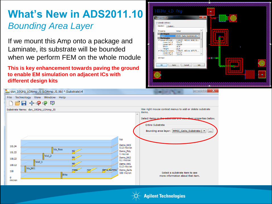
What’s New in ADS2011.10 Bounding Area Layer
If we mount this Amp onto a package and
Laminate, its substrate will be bounded
when we perform FEM on the whole module
This is key enhancement towards paving the ground
to enable EM simulation on adjacent ICs with
different design kits
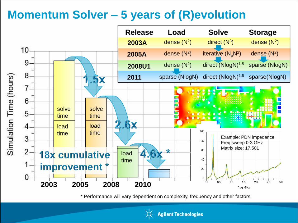
Example: PDN impedance
Freq sweep 0-3 GHz
Matrix size: 17.501
2005 2008 2010
solve
time
load
time
solve
time
load
time
load
time
2003
Release Load Solve Storage
2005A
2008U1
2011
dense (N2) direct (N3) dense (N2)
dense (N2) iterative (NpN2) dense (N2)
dense (N2) direct (NlogN)1.5 sparse (NlogN)
sparse (NlogN) direct (NlogN)1.5 sparse(NlogN)
2003A
Momentum Solver – 5 years of (R)evolution
* Performance will vary dependent on complexity, frequency and other factors
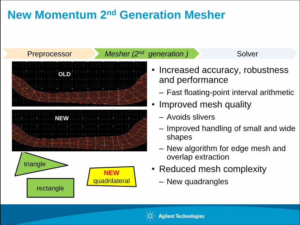
Preprocessor Mesher (2nd generation ) Solver
New Momentum 2nd Generation Mesher
• Increased accuracy, robustness and performance
– Fast floating-point interval arithmetic
• Improved mesh quality
– Avoids slivers
– Improved handling of small and wide shapes
– New algorithm for edge mesh and overlap extraction
• Reduced mesh complexity
– New quadrangles
rectangle
NEW
quadrilateral
triangle
OLD
NEW
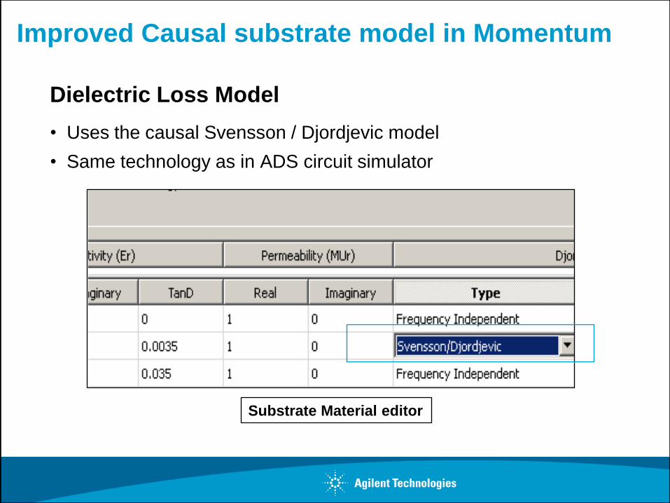
Improved Causal substrate model in Momentum
Dielectric Loss Model
• Uses the causal Svensson / Djordjevic model
• Same technology as in ADS circuit simulator
Substrate Material editor
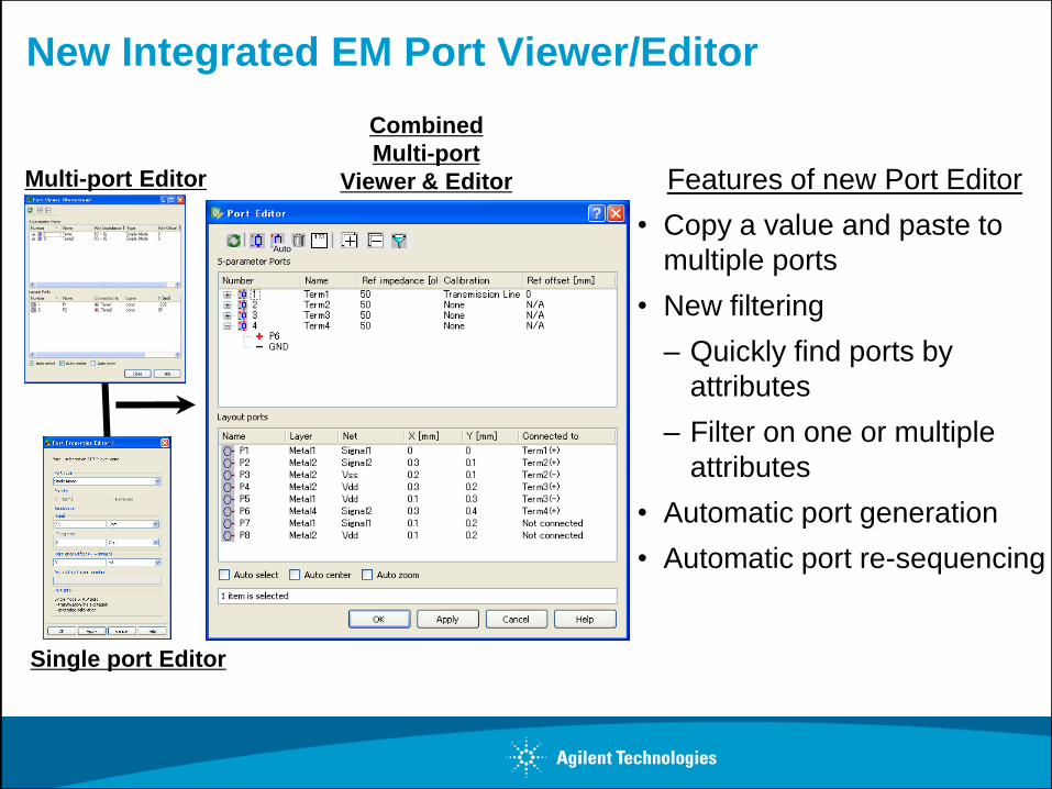
New Integrated EM Port Viewer/Editor
Features of new Port Editor
• Copy a value and paste to
multiple ports
• New filtering
– Quickly find ports by
attributes
– Filter on one or multiple
attributes
• Automatic port generation
• Automatic port re-sequencing
Auto
Multi-port Editor
Combined
Multi-port
Viewer & Editor
Single port Editor
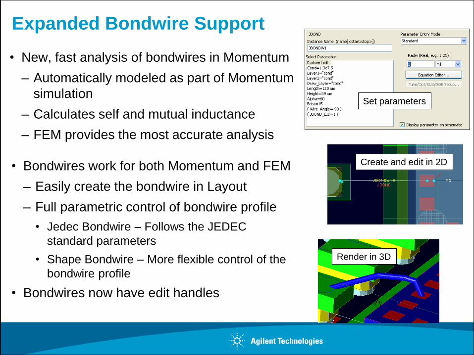
Expanded Bondwire Support
• New, fast analysis of bondwires in Momentum
– Automatically modeled as part of Momentum
simulation
– Calculates self and mutual inductance
– FEM provides the most accurate analysis
• Bondwires work for both Momentum and FEM
– Easily create the bondwire in Layout
– Full parametric control of bondwire profile
• Jedec Bondwire – Follows the JEDEC
standard parameters
• Shape Bondwire – More flexible control of the
bondwire profile
• Bondwires now have edit handles
Set parameters
Create and edit in 2D
Render in 3D
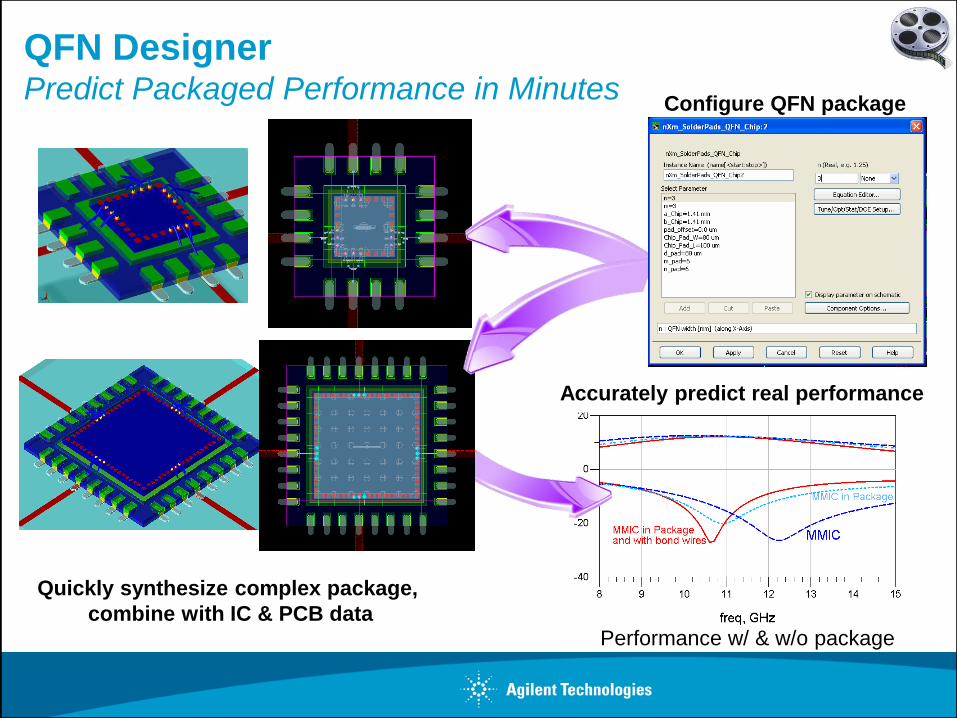
Performance w/ & w/o package
Accurately predict real performance
QFN Designer Predict Packaged Performance in Minutes
Quickly synthesize complex package,
combine with IC & PCB data
Configure QFN package
Extending MMIC technology description for easy and
accurate EM simulations of complex 3D structures
II) Emerging 3D Technologies
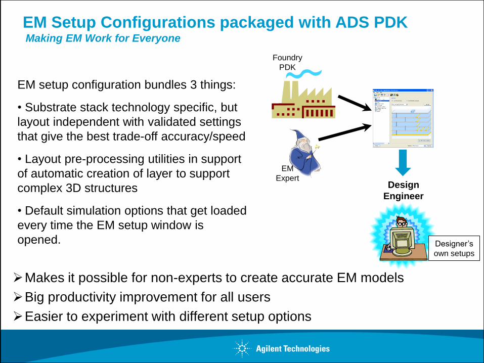
EM Setup Configurations packaged with ADS PDK Making EM Work for Everyone
Makes it possible for non-experts to create accurate EM models
Big productivity improvement for all users
Easier to experiment with different setup options
Foundry
PDK
EM
Expert Design
Engineer
Designer’s
own setups
EM setup configuration bundles 3 things:
• Substrate stack technology specific, but
layout independent with validated settings
that give the best trade-off accuracy/speed
• Layout pre-processing utilities in support
of automatic creation of layer to support
complex 3D structures
• Default simulation options that get loaded
every time the EM setup window is
opened.
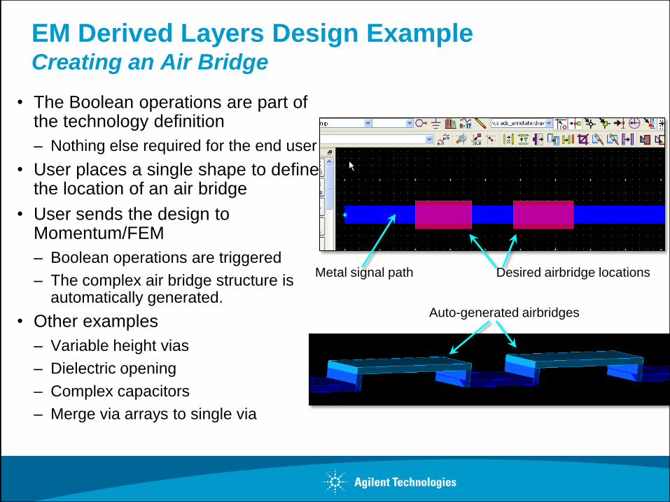
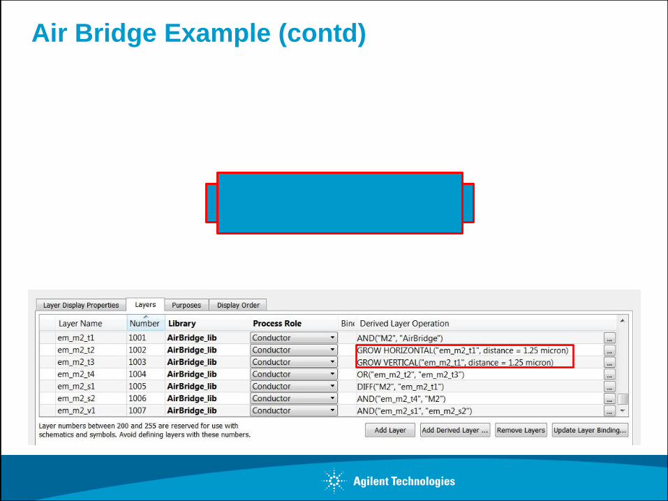
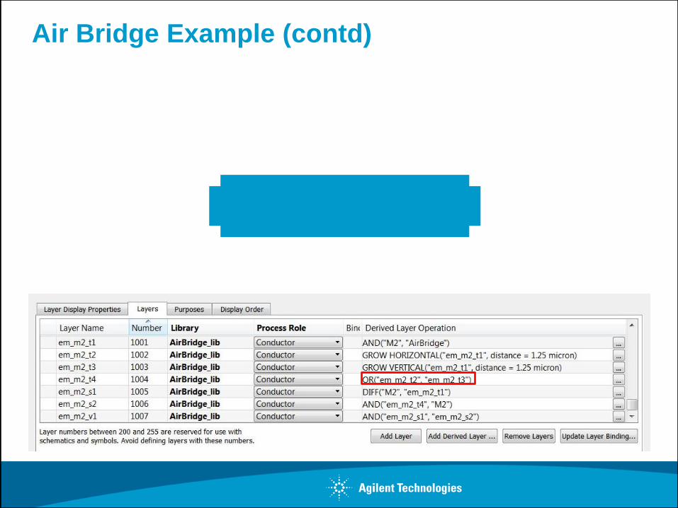
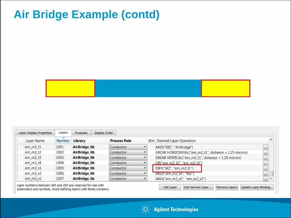
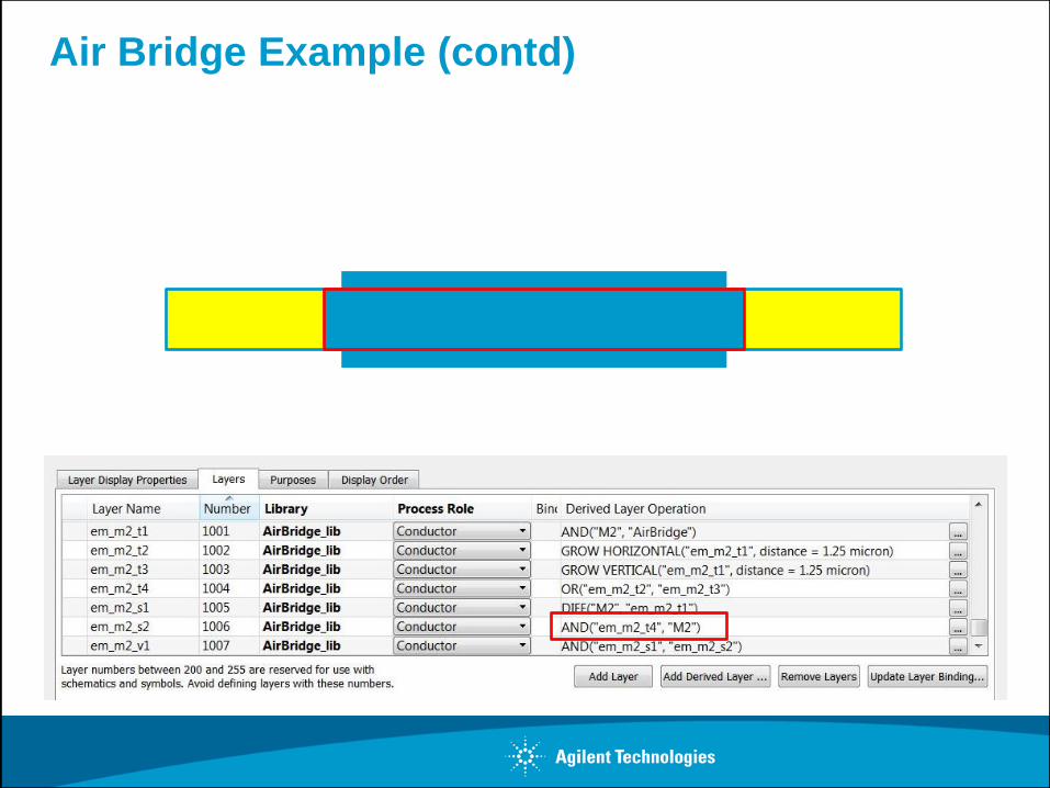
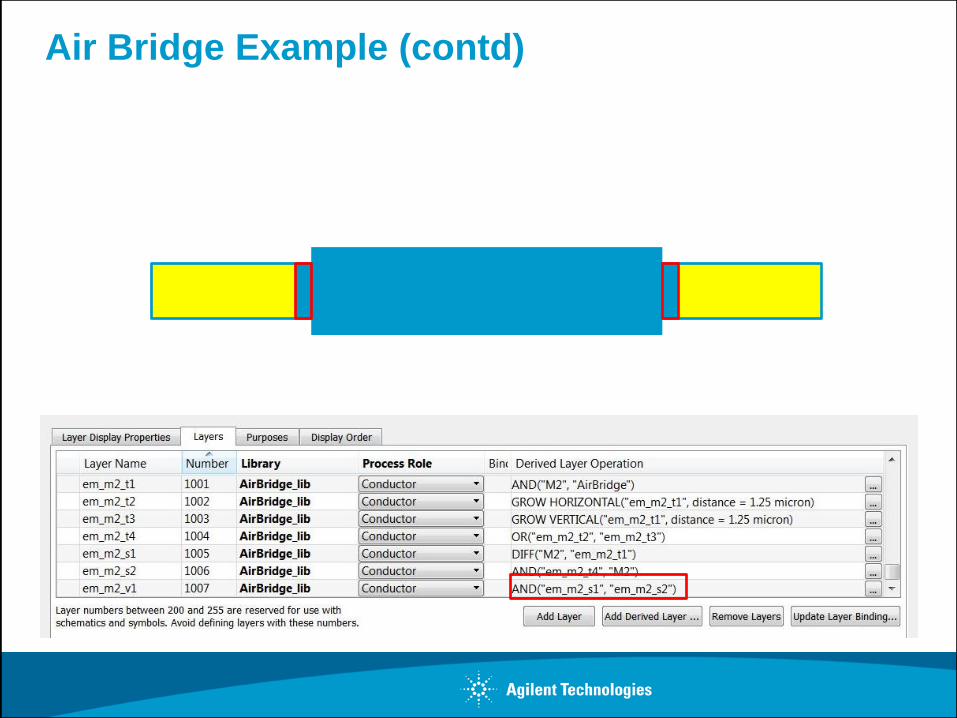
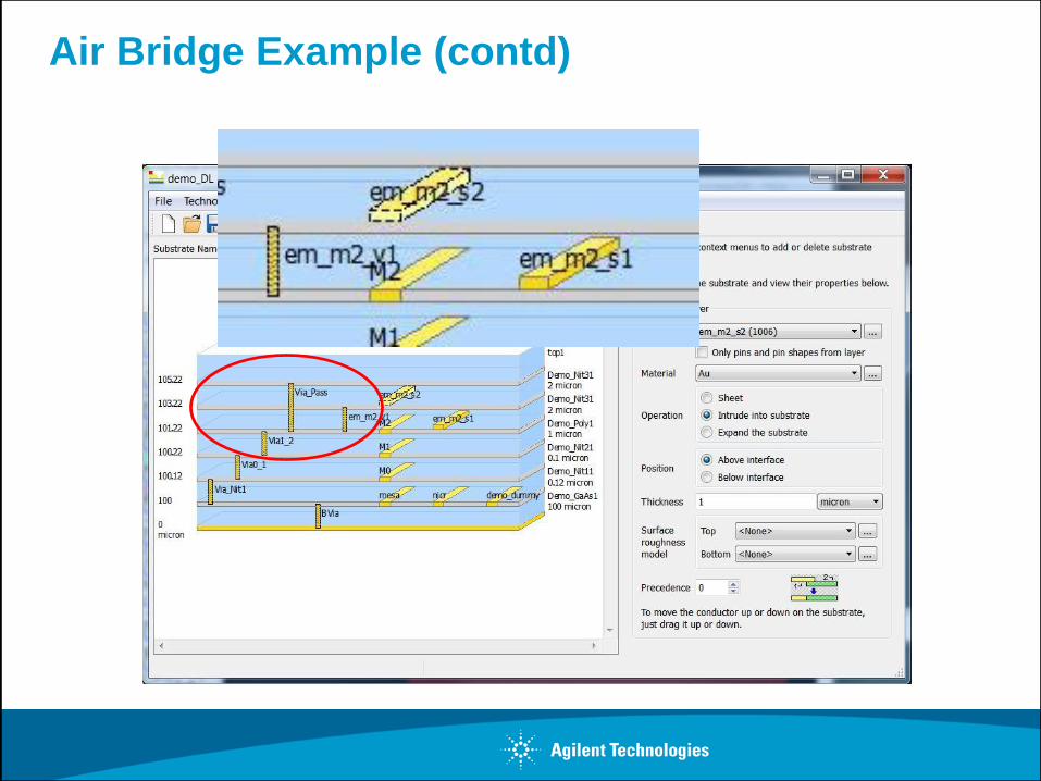
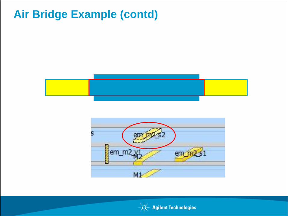
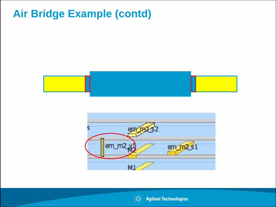
EM Derived Layers Design Example Creating an Air Bridge
• The Boolean operations are part of the technology definition
– Nothing else required for the end user
• User places a single shape to define the location of an air bridge
• User sends the design to Momentum/FEM
– Boolean operations are triggered
– The complex air bridge structure is automatically generated.
• Other examples
– Variable height vias
– Dielectric opening
– Complex capacitors
– Merge via arrays to single via
Metal signal path Desired airbridge locations
Auto-generated airbridges
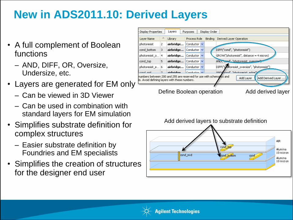
New in ADS2011.10: Derived Layers
• A full complement of Boolean functions
– AND, DIFF, OR, Oversize, Undersize, etc.
• Layers are generated for EM only
– Can be viewed in 3D Viewer
– Can be used in combination with standard layers for EM simulation
• Simplifies substrate definition for complex structures
– Easier substrate definition by Foundries and EM specialists
• Simplifies the creation of structures for the designer end user
Add derived layer Define Boolean operation
Add derived layers to substrate definition
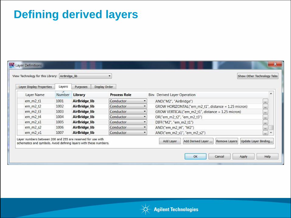
Defining derived layers
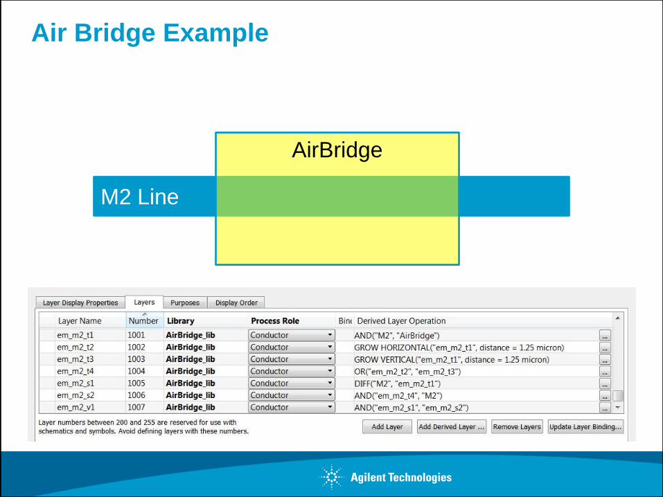
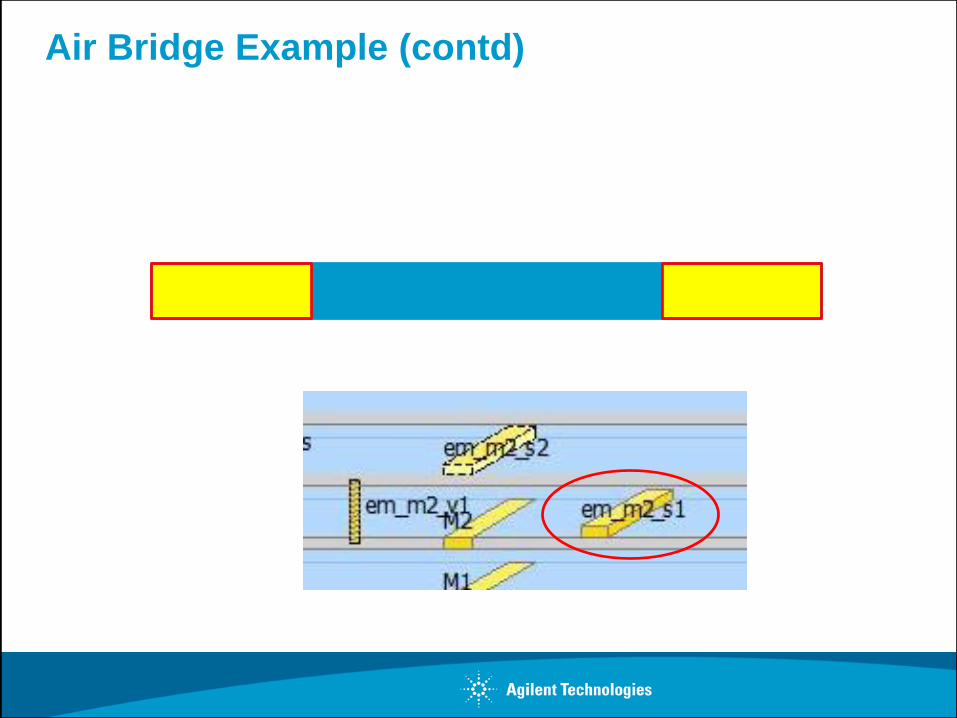
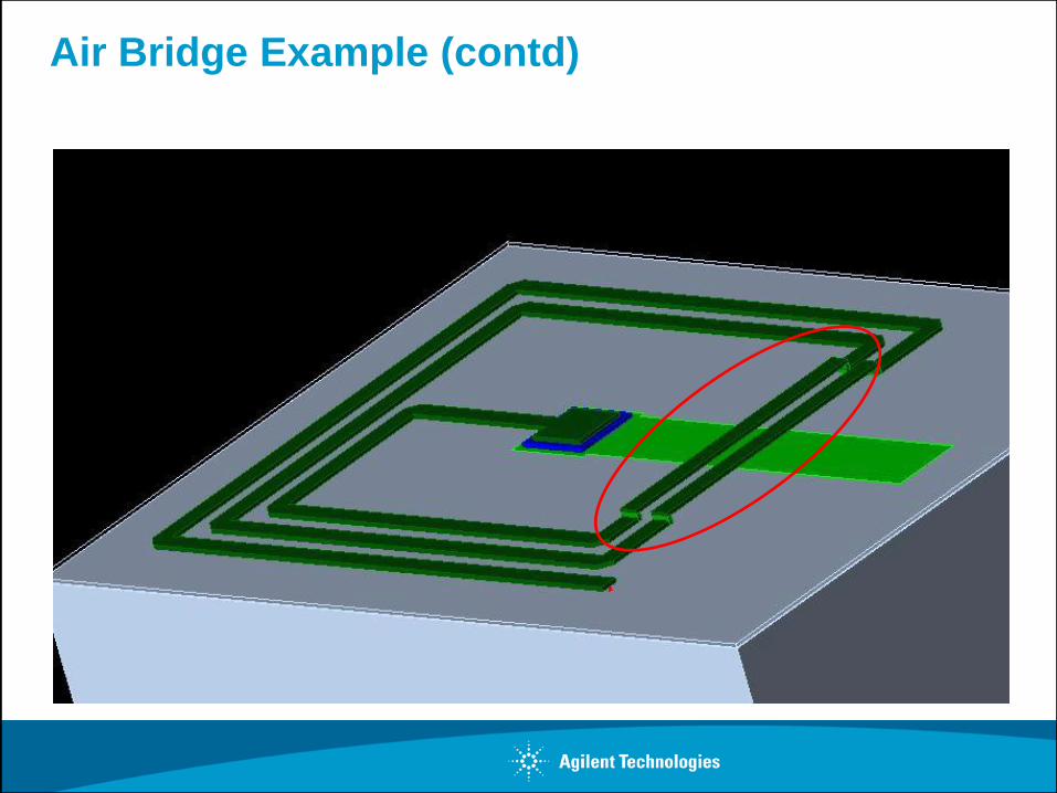
Air Bridge Example
M2 Line
AirBridge
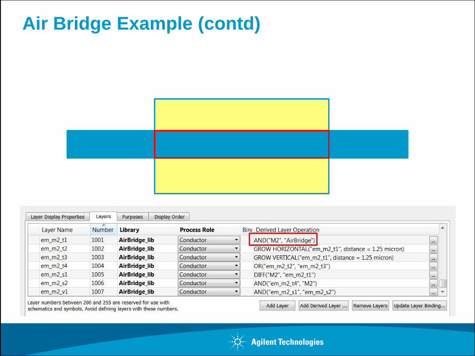
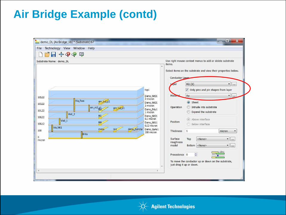
Air Bridge Example (contd)
Air Bridge Example (contd)
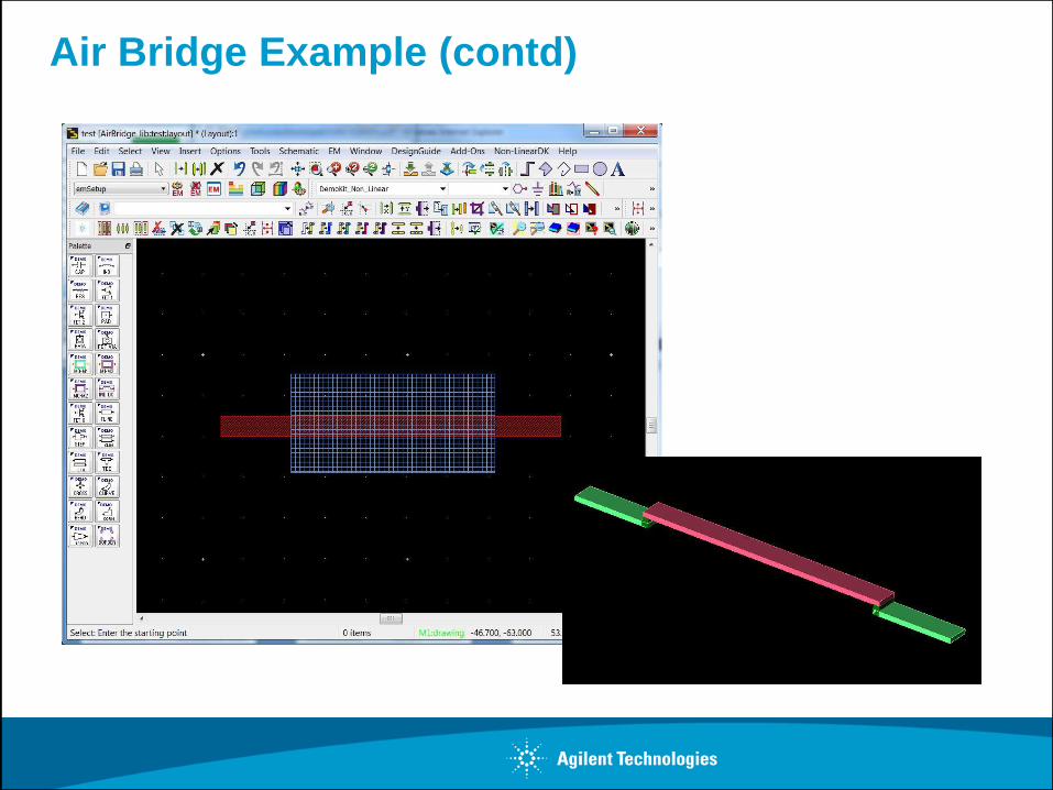
Air Bridge Example (contd)
Air Bridge Example (contd)
Air Bridge Example (contd)
Air Bridge Example (contd)
Air Bridge Example (contd)
Air Bridge Example (contd)
Air Bridge Example (contd)
Air Bridge Example (contd)
Air Bridge Example (contd)
Air Bridge Example (contd)
Air Bridge Example (contd)
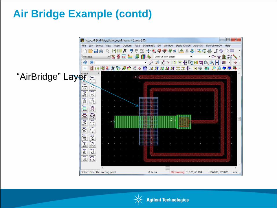
“AirBridge” Layer
Air Bridge Example (contd)
Air Bridge Example (contd)
For More Information
Agilent ADS 2011 Web page (new feature details)
www.agilent.com/find/eesof-ads2011
ADS 2011 on YouTube
www.youtube.com/user/AgilentEEsof
ADS 2011 Overview (Quick Start Video, Multi-technology Tutorials, …)
www.agilent.com/find/eesof-ads2011-overview
ADS 2011 Summary
• RF design has moved to complex ICs in multi-chip RF modules
• Today’s design flows are not able to address multiple technology design
• The IC, laminate, package, and PCB need to be designed together
• Electro-magnetic interactions between substrates need to be modeled
• ADS 2011 is the only EDA software able to address these multi-
technology design challenges
Agilent EEsof EDA
“Innovative Solutions,
Breakthrough Results”


![Tutorials for Layout, DRC, and LVS - Georgia Institute of ... for Layout, DRC, and LVS ... Choose option: No tech library needed ... Calibre Edit Verify Connectivity Options [abcd]](https://img.pdfslide.us/doc/110x75/5b4778b67f8b9a40638bee05/tutorials-for-layout-drc-and-lvs-georgia-institute-of-for-layout-drc-and.jpg)