Embed Size (px)
Citation preview

1
INF4420 / INF9425 INF4420 Projects inINF4420 / INF9425 INF4420 - Projects in analogue/mixed-signal CMOS design
Snorre Aunet ([email protected])
Nanoelectronics groupNanoelectronics group
Department of Informatics
University of Oslo
INF4420 / INF9425 – V2011:• M.Sc. Course:
• sa@padme ~ $ ng sinf4420
• thangln Nguyen Thang Le
• paulauds Paul Audun Sundar
j jj J J li J
• teachers:
• jonasjj Jonas Julian Jensen
• erikjsi Erik Simenstad
• magnutr Magnus Trandum
• patricd Patrick Dybwad
• oystebjo Øystein Bjørndal
• sohailmm Mahmood Sohali Musa
• abdulwm Majeed Abdul Wahab
• ejjohans Erlend Johan Johansen
• trymah Trym Hagen
• Martin Severin Orrebakken Haugland
• Kin-Keung Lee –”Kody”
• Snorre Aunettrymah Trym Hagen
• ramting Ramtin Ghirizadeh
• Ph.D. course:
• sa@padme ~ $ ng sinf9425
• andrelfe André Fernandes
27. januar 2011

2
INF4420 / INF3410
27. januar 2011
3
Outline – Tuesday 25th of January– Practical issues– Learning goals– Design project, tools and methods– Syllabus
V b i f i t d ti t i i it– Very brief introduction to various circuitbuilding blocks
(sample-and-holds, bandgap references, switched capacitor circuits, Nyquist- and oversampling data converters, oscillators phase-locked loops, CMOS technologyetc)

3
CMOS Integrated Circuits?
– Digital circuits exploit mainly transistors and interconnect
– Mixed-Signal (Digital AND Analog) also use resistors, capacitors and inductorsand inductors
– Work-horse of modern Information Technology
Moore’s law: exponential increase in components per area
• Challenge to integrate analog and digital (mixed-signal)

4
http://www.uio.no/studier/emner/matnat/ifi/INF4420/• INF4420 - Projects in analogue/mixed-signal CMOS design
• Course content - Learning outcomes - Admission - Prerequisites - Overlap - Teaching - Exam information - Other information - Contact us
• Facts about this course: Credits: 10 Level: Foundation course at bachelor's level Teaching semester: Every spring semester Examination semester: Every spring semester Language of instruction: English if requested by exchange students, otherwise Norwegian Administrated by: Department of Informatics (Ifi)Detailed course information - Current and previous semesters: Spring 2011
• Spring 2010
• Spring 2009
• Spring 2008
• Spring 2007
• Spring 2006
• Spring 2005
• Spring 2004
• Autumn 2003
• Course content
• The course provides the know-how and skills needed to design analogue and mixed-signal integrated circuit modules using modern program tools. The main focus of the course is complex systems such as data converters (A/D, D/A) and phase-locked loops (PLL). An introduction is given to CMOS technology and methods in order to implement passive components such as transistors, condensers and coils. In addition, matching, optimisation and noise deflection are all key aspects. The execution of project tasks will be a central part of the teaching.
• Learning outcomes
• Students will have the skills needed to design an integrated mixed-signal circuit in CMOS using modern design tools.
• Admission
• Students who are admitted to study programmes or individual courses at UiO must each semester register which courses and exams they wish to sign up for in StudentWeb.
• International applicants, if you are not already enrolled as a student at UiO, please see our information about admission requirements and procedures for international applicants.
• Prerequisites
• Formal prerequisites
• In addition to fulfilling the basic entrance requirements to higher education in Norway, applicants have to meet the following special admission requirements:
• Mathematics R1 or Mathematics (S1+S2)
• The special admission requirements may also be covered by equivalent studies from Norwegian upper secondary school or by other equivalent studies. Read more about special admission requirements.
• Overlap
• 10 credits against INF3420 - Prosjekter i analog/mixed-signal CMOS konstruksjon. 6 credits against INF239. 3 credits against INF238.
• Teaching
• 3 hours of lectures and 2 hours of working in groups every week. Some of the teaching will be given as supervision in labs.There are obligatory tasks to be handed in and passed in order to be admitted to take the exam.
• Exam information
• Individual grading of project assignment (50%)and final exam (ca 50%). Oral/written.
• Assessment and grading
• Course grades are awarded on a descending scale using alphabetic grades from A to E for passes and F for fail.
• Course Auditor: Per Olaf Pahr
• Other information
• The subject is regarded equal to INF3420 - Prosjekter i analog/mixed-signal CMOS konstruksjon when practicing exam regulations.
• Contact us
• Department of Informatics (Ifi)
• Visiting address:Informatics builidng, First floor, room 2316, Gaustadalléen 23
• Visiting hours:Monday-friday 12:00-15:00
• Postal address:P.o.Box 1080, BlindernNO-0316 Oslo
• Phone: +47 22 85 24 10 Fax: +47 22 85 24 01 E-mail: [email protected]: www.ifi.uio.no
•
Why ASICs (Application Specific Integrated Circuits) ??
– Advantages:
– Reduced size– Improved performance and functionalityp p y– Easier to hide ”company secrets”– Reduced cost– Reduced power consumption– Less radiated noise
– Disadvantages:– Increased start-up cost– High power density - Heat
H d t fi d t t– Hard to find top competence– Time consuming development and production– Substantial ”Time-to-market”

5
What is an integrated circuit?
– Transistors• Several options
– Capacitors• How to implementp• Linearity
– Resistors• How to implement• Area
– Inductors• How to implement• Quality factor
– Parasitic componentsC l l t• Calculate
• Minimize
Design methods; digital from HDL, full custom analog
– Digital systems:• Automatic• Automatic
synthesis–VHDL–Schematic
– Analog systems:• Module based• Module based• Full-custom

6
Low Power..
27. januar 2011
11
Mandatory design project
– Design and implement mixed-mode circuit:• Example: ADC, SC-filter, PLL, DAC ( 2008 )• System for automatic removal of mismatch (2009)System for automatic removal of mismatch (2009)• SAR Analog-to-Digital Converter (2010) • Milestones during the process• 2 persons in each group• Teaching assistant, Kin Keung Lee, will follow up
– Write a project report• LaTeX or similar
– Submission: Early in May– Counts 40 % in the final grading (exam 60%)

7
Challenge in 2008: Digital-to-Analog Converter (”DAC”)
27. januar 2011
13
INF4420 Project 2009 (1/2)
27. januar 2011
14

8
INF4420 project 2009 (2/2)
27. januar 2011
15
Project, 2010 (1/2)
test 16

9
Project, 2010 (2/2)
test 17
Cadence ( http://www.cadence.com/ )
– Widely used IC design tool worldwide, both in companies and academia
– Very large system– Very large system• PCB-design• IC-design
–Synthesis–Schematic entry–Simulator (Analog Environment / Spectre)Simulator (Analog Environment / Spectre)–Layout (Virtouso)
– DRC and LVS performed by Calibre (Mentor)
10
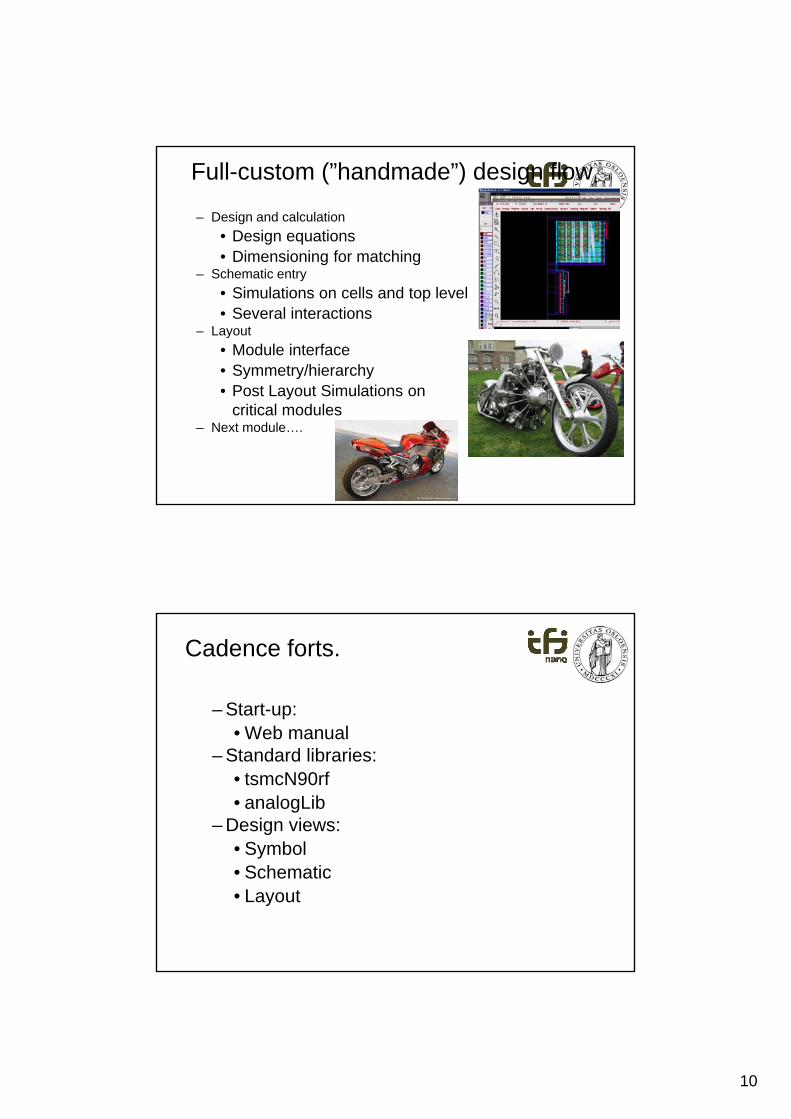
Full-custom (”handmade”) design flow
– Design and calculation
• Design equations• Dimensioning for matching
– Schematic entry
• Simulations on cells and top level• Several interactions
– Layout
• Module interface• Symmetry/hierarchy
P t L t Si l ti• Post Layout Simulations on critical modules
– Next module….
Cadence forts.
– Start-up:• Web manual• Web manual
– Standard libraries:• tsmcN90rf • analogLib
– Design views:• SymbolSymbol• Schematic• Layout

11
Schematic entry and simulations in Cadence
Symbol, schematic and layout (Cadence)
27. januar 2011
22

12
Process
–TSMC 90 nm low power CMOS:• Minimum gate length: 90nm• 1 Poly-layer• 9 Metal-layers• True triple well• Three different threshold voltages• Supply voltage: 1 2 V typSupply voltage: 1.2 V typ.• Very advanced process
AND-gate

13
Challenges regarding the project
– Project administration– Theoretical analysis and circuit design– Design errorsg
• LVS – Parasitic components
• Extraction and Post Layout Simulation (PLS)
– Process variations• Simulations (Corner + Monte-Carlo)Simulations (Corner + Monte Carlo)
– Noise• Component and crosstalk
– Good layout practice / Symmetry
Practical information– Lectures:
• Tuesdays . 9.15 – 11.00, Perl 2453 (should not collide with FYS3240).• From. 22/2: Tuesday . 9.15 – 12.00 ( Might be 9:15 – 11:00 in most cases )
– Syllabus:• Behzad Razavi: Design of Analog CMOS Integrated Circuits (from chap. 11-18.)• Selected additional material and lecture notes
LTH: Cadence 4 4• LTH: Cadence 4.4 • IFI: Lokal guide til Cadence
– Exercises• 2 hours per week – Perl 2453, wednesdays 12:15-14. Kin Keung Lee,
[email protected]– Project supervision/design lab
• 2/4 hours each week – Time: 12:15-14:00. Martin S. O. Haugland, [email protected], Kin Keung (”Kody”) Lee .
• Ole Johan Dahls hus; Chill 3443– Software:
• Cadence 5.00 or 6.00 ((?))TSMC 90 d i kit• TSMC 90 nm design kit
– Where to run the software:• Win PC running X-Win connected to Linux server /remote desktop and Linux• Linux computer
– Student reference group• 1-2 students

14
What do we expect from you? • The course is demanding
• Theoretical backgroundINF3410 l i l t i i il– INF3410 analog microelectronics, or similar
– FYS3220 linear circuit theory, or similar– INF3440 signal processing, or similar
• Prepare for the lectures
• Exercises
• Use the reference group and course evaluations to id f db k t th INF4420 t ffprovide feedback to the INF4420 staff
Final exam – a few words
• Thursday 6th of June, starting 14:30 (4 hours)
• Problems usually related to most of the relevant chapters in the book (11-18), and material from the lectures
convert todiscrete-time
sequenceDSP
convert toimpulse
trainhold
analog
low-passfilter
xc t( )
s t( )
xs t( )
x n( ) xc nT( )=y n( ) ys t( ) ysh t( )
yc t( )
DSPA/D
converter
sample analog
low-passfilter
andhold
D/Aconverter
with hold
xc t( )
xsh t( ) x n( ) xc nT( )= y n( )ysh t( )
yc t( )

15
Syllabus; chapters 11-18 (Razavi)+ data converters (Johns & Martin ++)
• Chapter 11 Bandgap references
• Chapter 12 Introduction to Switched Capacitor Circuits
Ch t 13 N li it d i t h• Chapter 13 Nonlinearity and mismatch
• Chapter 14 Oscillators
• Chapter 15 Phase-locked loops
• Chapter 16 Short-Channel effects and Device models
• Chapter 17 CMOS processing technology
• Chapter 18 Layout and packaging• Chapter 18 Layout and packaging
• Chapter 14 in J&M
• Oversampling converters + additional
material on data converters
Bandgap references (chapter 11 in Razavi)
27. januar 2011
30

16
Chapter 12 Intro to Switched Cap.circuits
v nT( )
21
C1
V1 V2V1 V2
Re q
Req
TC
1
------=Q C
1V
1V
2– every clock period=
21
C2
C1
vo
n( ) vco
nT( )=vi
n( ) vc i
nT( )=
1
vc i
t( )
vcx
t( )
vco
t( )
c2( )
vc1
t( )
Chapter 13 Nonlinearity and mismatch • Nonlinearity
• Mismatch

17
Data converter fundamentals • Ideal D/A and A/D
• Quantization noise
• Signed codes• Signed codes
• Performance limitations
Nyquist-Rate D/A Converters• Decoder-based converters
• Binary-scaled converters
• Thermometer-code converters• Thermometer-code converters
• Hybrid conv.
D/ABinVout
Vref

18
Nyquist-Rate A/D Converters• Integrating converters
• Successive approx. converters
• Algorithmic converters VrefAlgorithmic converters
• Flash (parallell) conv.
• Two-step, interpolating,
• Folding, pipelined conv.
Vin
(2N–1) to N
encoder
N digitaloutputs
Over range
R
R
R
R
R
Vr3
Vr4
Vr5
Vr6
Vr7
R2----
Comparators
R
R
Vr1
Vr2
r3
R 2
Two consequences of the Nyquist-theorem and anti-aliasing filters (Wikipedia):
• If the highest frequency B in the original signal is known, the theorem gives the lower bound on the sampling frequency for which perfect reconstruction can be assured. This lower bound to the sampling frequency, 2B, is called the Nyquist rate.
• If instead the sampling frequency is known, the theorem gives us an upper bound for frequency components, B<fs/2, of the signal to allow for perfect reconstruction. This upper bound is the Nyquist frequency, denoted fN.
• An anti-aliasing filter is a filter used before a signal sampler, to restrict the bandwidth of a signal to approximately satisfy the sampling theorem. Since the theorem states that unambiguous interpretation of the signal f it l i ibl l h th f f i t idfrom its samples is possible only when the power of frequencies outside the Nyquist bandwidth is zero, the anti-aliasing filter would have to have perfect stop-band rejection to completely satisfy the theorem. Every realizable anti-aliasing filter will permit some aliasing to occur; the amount of aliasing that does occur depends on how good the filter is.

19
Chapter 14 in ”Johns & Martin”OversamplingConverters
• Oversampling ( >> 2 Nyquist bandwidth) relaxes requirements for matchingrequirements for matching
• High resolution, low to medium speed
• Noise shaping & oversampling
• N+1 order modulator gives a certain SNR for lower OSR
than N-order mod.
• 24 bit Audio conv.
Chapter 14 (”Razavi”) Oscillators

20
Chapter 15 Phase-locked loops
• Application examples:
• clock multiplication• clock multiplication,• Freq. generation: The PLL output is a signal with frequency N times the input
frequency where N may be a fractional number
• FM demodulation (The input is a FM signal (IF) The output is the demodulated baseband signal
• Products: TV and wireless
GainLow-pass
filterV
Phase
detector
VCOVcntl
Outputvoltage
Vosc
Average voltage proportional to phase difference
VinVpd
KlpHlp s( )
Vlp
(voltage controlled oscillator)
Chapter 16 Short-Channel Effects and Device Models

21
Chapter 17 CMOS Processing Technology
Published: Monday, Jan. 24, 2011 / Updated: Monday, Jan. 24, 2011 08:08 AMAltera Unveils 28-nm Device Portfolio Tailored to Customers' Diverse Design RequirementsIndustry's Most Diverse Product Offering Meets Expanding System g p g yNeeds in Performance, Power and Cost
Chapter 18 Layout and Packaging

22
www.akademika.no / www.amazon.co.uk
4327. januar 2011
Next week:
• Sample and Hold circuits ++p
• Messages are given on the INF4420 homepage.
• Questions: [email protected] , 22852703 / 90013264

23
45