Embed Size (px)
Citation preview
12 V ± 16 V from Upstream
Supply
TPS22810 12V_Audio
Buck
TPS564201
Buck
TPS566250
TPS22975 TLV759
5V_USB
WIFI
Ethernet
3.3 V
1V1_Core
TPS229195 V
TLV755 TPS229191.8 V
1.5V_
DRAM
Discrete_FET
Discrete_FET
Discrete_FET
3V3_
STBY
5 V
TV TunerxTPS22919
TPS2595
3V3_
TCONTPS22919
12V_TCON
NAND, eMMC, I/O
TLV62569A
TLV62568
TPS22919
TPS25221
5V_EEPROM
Load Switches / eFuse / Supervisor
DC-DC / LDOs
TLV809E
TLV809E
1TIDUEO4B–April 2019–Revised November 2019Submit Documentation Feedback
Copyright © 2019, Texas Instruments Incorporated
Multi-rail TV Power Supply Reference Design With Flexible Partitioning toMaximize Power Savings
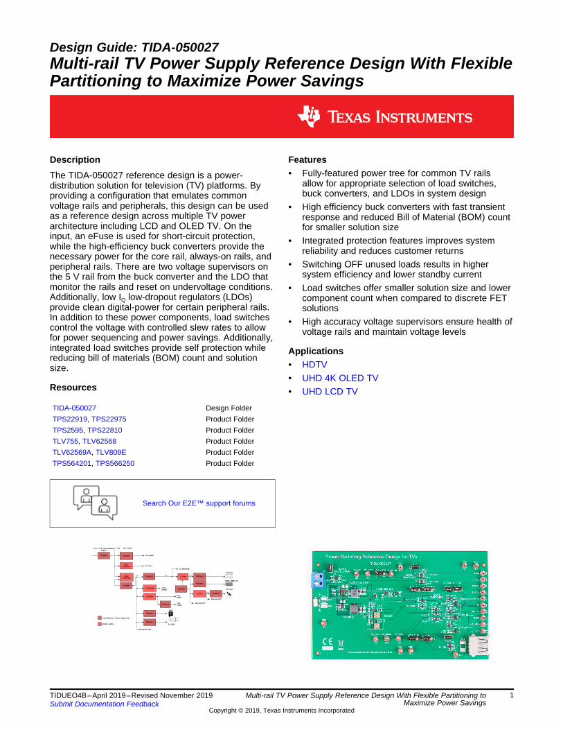
Design Guide: TIDA-050027Multi-rail TV Power Supply Reference Design With FlexiblePartitioning to Maximize Power Savings
DescriptionThe TIDA-050027 reference design is a power-distribution solution for television (TV) platforms. Byproviding a configuration that emulates commonvoltage rails and peripherals, this design can be usedas a reference design across multiple TV powerarchitecture including LCD and OLED TV. On theinput, an eFuse is used for short-circuit protection,while the high-efficiency buck converters provide thenecessary power for the core rail, always-on rails, andperipheral rails. There are two voltage supervisors onthe 5 V rail from the buck converter and the LDO thatmonitor the rails and reset on undervoltage conditions.Additionally, low IQ low-dropout regulators (LDOs)provide clean digital-power for certain peripheral rails.In addition to these power components, load switchescontrol the voltage with controlled slew rates to allowfor power sequencing and power savings. Additionally,integrated load switches provide self protection whilereducing bill of materials (BOM) count and solutionsize.
Resources
TIDA-050027 Design FolderTPS22919, TPS22975 Product FolderTPS2595, TPS22810 Product FolderTLV755, TLV62568 Product FolderTLV62569A, TLV809E Product FolderTPS564201, TPS566250 Product Folder
Search Our E2E™ support forums
Features• Fully-featured power tree for common TV rails
allow for appropriate selection of load switches,buck converters, and LDOs in system design
• High efficiency buck converters with fast transientresponse and reduced Bill of Material (BOM) countfor smaller solution size
• Integrated protection features improves systemreliability and reduces customer returns
• Switching OFF unused loads results in highersystem efficiency and lower standby current
• Load switches offer smaller solution size and lowercomponent count when compared to discrete FETsolutions
• High accuracy voltage supervisors ensure health ofvoltage rails and maintain voltage levels
Applications• HDTV• UHD 4K OLED TV• UHD LCD TV
System Description www.ti.com
2 TIDUEO4B–April 2019–Revised November 2019Submit Documentation Feedback
Copyright © 2019, Texas Instruments Incorporated
Multi-rail TV Power Supply Reference Design With Flexible Partitioning toMaximize Power Savings
An IMPORTANT NOTICE at the end of this TI reference design addresses authorized use, intellectual property matters and otherimportant disclaimers and information.
1 System DescriptionThis reference design showcases a power distribution solution for televisions (TVs). Since many TVarchitectures require similar core voltage and peripheral rails, this design can be used across multiple TVarchitectures including OLED and LCD TVs.
This design incorporates four buck converters as well as two LDOs to power the core rails, always-onrails, memory, and peripherals such as USB ports and TV tuner. Each buck converter is chosen to handlespecific requirements for each of the rails. For the core rail, the requirements include steady outputvoltage with very good transient response to avoid affecting performance. The remainder of the railsrequire high efficiency with good transient response. The LDOs for the peripherals provide a IQ powersupply that also require a clean-power supply such as the TV Tuner.
This design also incorporates nine load switches for peripheral loads commonly found on most TVsincluding: Panel Power (TCON), Stand-by (STBY) rails, WIFI, NAND, USB, and TV Tuner blocks. All ofthe load switches have their ON pins connected to external jumpers for quick access to each peripheralrail. An eFuse at the input manages short-circuit and overvoltage events that could potentially damagedownstream DC/DC converters and load switches. The reference design also includes common voltagerails found in most TV solutions, including 5 V Peripheral, 3.3 V Standby, 1.5 V DRAM, 3.3 V I/O, and 1.1V Core rail. Finally, a USB-A header is included at the output of the 5 V USB switch to support USB loads.By using integrated devices, this reference design reduces BOM count, improves system reliability, andenables faster design cycles.
Each main voltage rail (5 V, 3.3 V, and 1.8 V) is accompanied by a discrete FET solution. This allows adirect performance comparison between the integrated load switch and a discrete FET solution. Testpoints are included at the output of each peripheral and voltage rail, and silkscreen traces outline the sizeof each solution.
www.ti.com System Description
3TIDUEO4B–April 2019–Revised November 2019Submit Documentation Feedback
Copyright © 2019, Texas Instruments Incorporated
Multi-rail TV Power Supply Reference Design With Flexible Partitioning toMaximize Power Savings
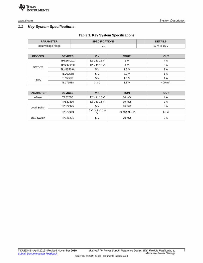
1.1 Key System Specifications
Table 1. Key System Specifications
PARAMETER SPECIFICATIONS DETAILSInput voltage range VIN 12 V to 16 V
DEVICES DEVICES VIN VOUT IOUT
DC/DCS
TPS564201 12 V to 16 V 5 V 4 ATPS566250 12 V to 16 V 1 V 6 ATLV62569A 5 V 1.5 V 2 ATLV62568 5 V 3.3 V 1 A
LDOsTLV759P 5 V 1.8 V 1 ATLV75518 3.3 V 1.8 V 400 mA
PARAMETER DEVICES VIN RON IOUTeFuse TPS2595 12 V to 16 V 34 mΩ 4 A
Load Switch
TPS22810 12 V to 16 V 79 mΩ 2 ATPS22975 5 V 16 mΩ 6 A
TPS22919 5 V, 3.3 V, 1.8V 89 mΩ at 5 V 1.5 A
USB Switch TPS25221 5 V 70 mΩ 2 A
12 V ± 16 V from Upstream
Supply
TPS22810 12V_Audio
Buck
TPS564201
Buck
TPS566250
TPS22975 TLV759
5V_USB
WIFI
Ethernet
3.3 V
1V1_Core
TPS229195 V
TLV755 TPS229191.8 V
1.5V_
DRAM
Discrete_FET
Discrete_FET
Discrete_FET
3V3_
STBY
5 V
TV TunerxTPS22919
TPS2595
3V3_
TCONTPS22919
12V_TCON
NAND, eMMC, I/O
TLV62569A
TLV62568
TPS22919
TPS25221
5V_EEPROM
Load Switches / eFuse / Supervisor
DC-DC / LDOs
TLV809E
TLV809E
System Overview www.ti.com
4 TIDUEO4B–April 2019–Revised November 2019Submit Documentation Feedback
Copyright © 2019, Texas Instruments Incorporated
Multi-rail TV Power Supply Reference Design With Flexible Partitioning toMaximize Power Savings
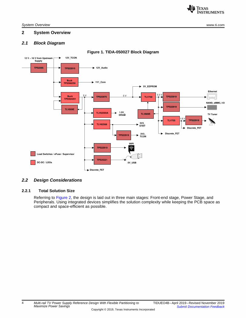
2 System Overview
2.1 Block Diagram
Figure 1. TIDA-050027 Block Diagram
2.2 Design Considerations
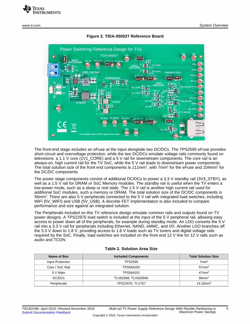
2.2.1 Total Solution SizeReferring to Figure 2, the design is laid out in three main stages: Front-end stage, Power Stage, andPeripherals. Using integrated devices simplifies the solution complexity while keeping the PCB space ascompact and space-efficient as possible.
www.ti.com System Overview
5TIDUEO4B–April 2019–Revised November 2019Submit Documentation Feedback
Copyright © 2019, Texas Instruments Incorporated
Multi-rail TV Power Supply Reference Design With Flexible Partitioning toMaximize Power Savings
Figure 2. TIDA-050027 Reference Board
The front-end stage includes an eFuse at the input alongside two DC/DCs. The TPS2595 eFuse providesshort-circuit and overvoltage protection, while the two DC/DCs emulate voltage rails commonly found ontelevisions: a 1.1 V core (1V1_CORE) and a 5 V rail for downstream components. The core rail is analways-on, high current rail for the TV SoC, while the 5 V rail leads to downstream power components.The total solution size of the front end components is 111mm2, with 7mm2 for the eFuse and 104mm2 forthe DC/DC components.
The power stage components consist of additional DC/DCs to power a 3.3 V standby rail (3V3_STBY), aswell as a 1.5 V rail for DRAM or SoC Memory modules. The standby rail is useful when the TV enters alow-power mode, such as a sleep or rest state. The 1.5 V rail is another high current rail used foradditional SoC modules, such a memory or DRAM. The total solution size of the DC/DC components is56mm2. There are also 5 V peripherals connected to the 5 V rail with integrated load switches, includingWiFi (5V_WIFI) and USB (5V_USB). A discrete FET implementation is also included to compareperformance and size against an integrated solution.
The Peripherals included on this TV reference design emulate common rails and outputs found on TVpower designs. A TPS22975 load switch is included at the input of the 5 V peripheral rail, allowing easyaccess to power down all of the peripherals, for example during standby mode. An LDO converts the 5 Vrail into a 3.3 V rail for peripherals including Ethernet, NAND, eMMC, and I/O. Another LDO branches offthe 3.3 V down to 1.8 V, providing access to 1.8 V loads such as TV tuners and digital voltage railsrequired by the SoC. Finally, load switches are included on the front end 12 V line for 12 V rails such asaudio and TCON.
Table 2. Solution Area Size
Name of Box Included Components Total Solution SizeInput Protection TPS2595 7mm2
Core / SoC Rail TPS566250 57mm2
5 V Main TPS564201 47mm2
DC/DCs TLV62568, TLV62569A 56mm2
Peripherals TPS22975, TLV757 14.18mm2
100 1 �F1 �F
1 k
0.1 �F
VIN VOUT
ON
L1 �F
+
±
VIN
Upstream LoadGND
H
IN
ON0.1 �F
CL CL
RL
Downstream Load
QOD
System Overview www.ti.com
6 TIDUEO4B–April 2019–Revised November 2019Submit Documentation Feedback
Copyright © 2019, Texas Instruments Incorporated
Multi-rail TV Power Supply Reference Design With Flexible Partitioning toMaximize Power Savings
2.2.2 Power Switching Complexity and SizeAs televisions push for higher resolution and greater complexity, their power designs are also gettinglarger and more complex. As the number of power rails and peripherals increases, additional devices andpassive components need to be selected and integrated into the system. As the BOM complexityincreases, the number of design considerations increase: including design and layout cycles, PCB space,and points of failure/visual inspection.
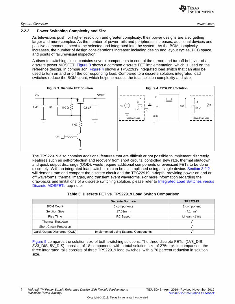
A discrete switching circuit contains several components to control the turnon and turnoff behavior of adiscrete power MOSFET. Figure 3 shows a common discrete FET implementation, which is used on thereference design. In comparison, Figure 4 shows a TPS22919 integrated load switch that can also beused to turn on and or off the corresponding load. Compared to a discrete solution, integrated loadswitches reduce the BOM count, which helps to reduce the total solution complexity and size.
Figure 3. Discrete FET Solution Figure 4. TPS22919 Solution
The TPS22919 also contains additional features that are difficult or not possible to implement discretely.Features such as self-protection and recovery from short circuits, controlled slew rate, thermal shutdown,and quick output discharge (QOD), would require additional components or oversized FETs to be donediscretely. With an integrated load switch, this can be accomplished using a single device. Section 3.2.2will demonstrate and compare the discrete circuit and the TPS22919 in-depth, providing power on and oroff waveforms, thermal images, and transient event waveforms. For more information regarding thedrawbacks and limitations of a discrete switching solution, please refer to Integrated Load Switches versusDiscrete MOSFETs app note.
Table 3. Discrete FET vs. TPS22919 Load Switch Comparison
Discrete Solution TPS22919BOM Count 6 components 1 component
Solution Size 17.08mm2 4.1mm2
Rise Time RC Based Linear, ~1 msThermal Shutdown ✓✓
Short Circuit Protection ✓✓Quick Output Discharge (QOD) Implemented using External Components ✓✓
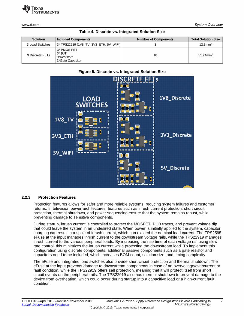
Figure 5 compares the solution size of both switching solutions. The three discrete FETs, (1V8_DIS,3V3_DIS, 5V_DIS), consists of 18 components with a total solution size of 275mm2. In comparison, thethree integrated rails consists of three TPS22919 load switches, with a 76 percent reduction in solutionsize.
www.ti.com System Overview
7TIDUEO4B–April 2019–Revised November 2019Submit Documentation Feedback
Copyright © 2019, Texas Instruments Incorporated
Multi-rail TV Power Supply Reference Design With Flexible Partitioning toMaximize Power Savings
Table 4. Discrete vs. Integrated Solution Size
Solution Included Components Number of Components Total Solution Size3 Load Switches 3* TPS22919 (1V8_TV, 3V3_ETH, 5V_WIFI) 3 12.3mm2
3 Discrete FETs
3* PMOS FET3* BJT9*Resistors3*Gate Capacitor
18 51.24mm2
Figure 5. Discrete vs. Integrated Solution Size
2.2.3 Protection FeaturesProtection features allows for safer and more reliable systems, reducing system failures and customerreturns. In television power architectures, features such as inrush current protection, short circuitprotection, thermal shutdown, and power sequencing ensure that the system remains robust, whilepreventing damage to sensitive components.
During startup, inrush current is controlled to protect the MOSFET, PCB traces, and prevent voltage dipthat could leave the system in an undesired state. When power is initially applied to the system, capacitorcharging can result in a spike of inrush current, which can exceed the nominal load current. The TPS2595eFuse at the input manages inrush current to the downstream voltage rails, while the TPS22919 managesinrush current to the various peripheral loads. By increasing the rise time of each voltage rail using slewrate control, this minimizes the inrush current while protecting the downstream load. To implement thisconfiguration using discrete components, additional passive components such as a gate resistor andcapacitors need to be included, which increases BOM count, solution size, and timing complexity.
The eFuse and integrated load switches also provide short circuit protection and thermal shutdown. TheeFuse at the input prevents damage to downstream components in case of an overvoltage/overcurrent orfault condition, while the TPS22919 offers self protection, meaning that it will protect itself from shortcircuit events on the peripheral rails. The TPS22919 also has thermal shutdown to prevent damage to thedevice from overheating, which could occur during startup into a capacitive load or a high-current faultcondition.
12 V ± 16 V from Upstream
Supply
TPS564201
TPS566250
TLV759
1V1_Core
TLV755
3V3_
STBY
5 V
TLV62569A
TLV62568
5 V
3.3 V
1.8 V
1.5V_DRAM
12 V ± 16 V
On / Off
System Overview www.ti.com
8 TIDUEO4B–April 2019–Revised November 2019Submit Documentation Feedback
Copyright © 2019, Texas Instruments Incorporated
Multi-rail TV Power Supply Reference Design With Flexible Partitioning toMaximize Power Savings
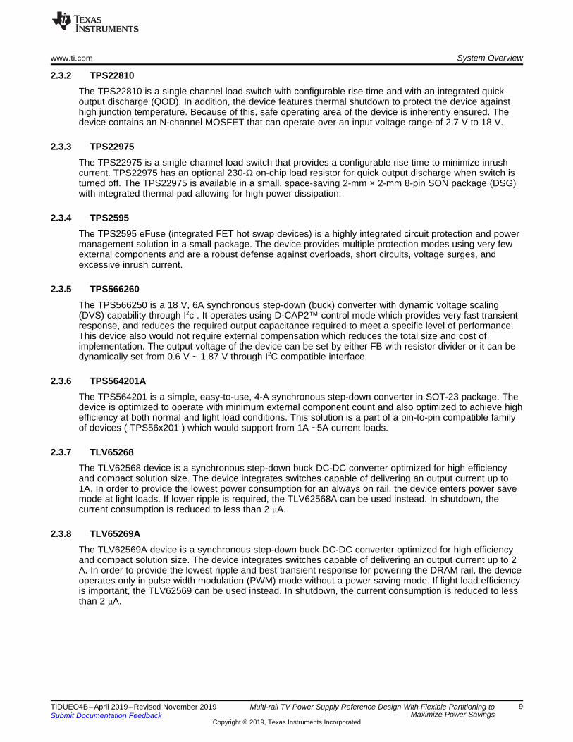
The voltage supervisor allows for monitoring of the buck converter and LDO for undervoltage conditionsand turn off appropriately when they reach below the voltage thresholds for each device. When thevoltage at the output of these devices falls below the set voltage thresholds for the voltage supervisors,they will output an active-low signal from the RESET pin to disable the devices.
2.2.4 Power ConsumptionTo reduce standby power for the system, this reference design reduces power consumption by choosinghigh efficiency and low IQ power components and by disconnecting loads and peripherals from DC/DCconverters when not in use, which is common practice in standby mode.
In this design, load switches are used to emulate various peripheral rails, which can be turned on or offwhen not in use. If the TV requires all the peripherals to be off in a certain mode, such as standby mode,the TPS22975 can also be used to turn off all the various peripheral rails. The switches can also be usedfor power sequencing. Power Sequencing is critical for voltage rails that must turn on in a specific order toensure operation safety and reliability. Sequencing the rails also staggers the inrush current duringstartup, which reduces system stress and prevents unexpected reverse bias conditions. On this TV powerdesign, the load switches can be sequenced to ensure that the core rails (1V1_CORE, DRAM, Panel), areup before the peripheral rails are operational.
Televisions also contain always-on rails to power critical system components such as core SoC rails,standby rails, and DRAM power. These rails must remain on throughout all operation modes. Therefore,all of the four DC/DC converters remain enabled to emulate powering always-on loads.
Figure 6. Power Tree
2.3 Highlighted Products
2.3.1 TPS22919The TPS22919 device is a small, single channel load switch with controlled slew rate. When power is firstapplied, a Smart Pull Down is used to keep the ON pin from floating until system sequencing is complete.When the pin is deliberately driven High (>VIH), the Smart Pull Down is disconnected to preventunnecessary power loss. The TPS22919 load switch is also self-protected, meaning that it will protectitself from short circuit events on the output of the device. It also has thermal shutdown to prevent anydamage from overheating.
www.ti.com System Overview
9TIDUEO4B–April 2019–Revised November 2019Submit Documentation Feedback
Copyright © 2019, Texas Instruments Incorporated
Multi-rail TV Power Supply Reference Design With Flexible Partitioning toMaximize Power Savings
2.3.2 TPS22810The TPS22810 is a single channel load switch with configurable rise time and with an integrated quickoutput discharge (QOD). In addition, the device features thermal shutdown to protect the device againsthigh junction temperature. Because of this, safe operating area of the device is inherently ensured. Thedevice contains an N-channel MOSFET that can operate over an input voltage range of 2.7 V to 18 V.
2.3.3 TPS22975The TPS22975 is a single-channel load switch that provides a configurable rise time to minimize inrushcurrent. TPS22975 has an optional 230-Ω on-chip load resistor for quick output discharge when switch isturned off. The TPS22975 is available in a small, space-saving 2-mm × 2-mm 8-pin SON package (DSG)with integrated thermal pad allowing for high power dissipation.
2.3.4 TPS2595The TPS2595 eFuse (integrated FET hot swap devices) is a highly integrated circuit protection and powermanagement solution in a small package. The device provides multiple protection modes using very fewexternal components and are a robust defense against overloads, short circuits, voltage surges, andexcessive inrush current.
2.3.5 TPS566260The TPS566250 is a 18 V, 6A synchronous step-down (buck) converter with dynamic voltage scaling(DVS) capability through I2c . It operates using D-CAP2™ control mode which provides very fast transientresponse, and reduces the required output capacitance required to meet a specific level of performance.This device also would not require external compensation which reduces the total size and cost ofimplementation. The output voltage of the device can be set by either FB with resistor divider or it can bedynamically set from 0.6 V ~ 1.87 V through I2C compatible interface.
2.3.6 TPS564201AThe TPS564201 is a simple, easy-to-use, 4-A synchronous step-down converter in SOT-23 package. Thedevice is optimized to operate with minimum external component count and also optimized to achieve highefficiency at both normal and light load conditions. This solution is a part of a pin-to-pin compatible familyof devices ( TPS56x201 ) which would support from 1A ~5A current loads.
2.3.7 TLV65268The TLV62568 device is a synchronous step-down buck DC-DC converter optimized for high efficiencyand compact solution size. The device integrates switches capable of delivering an output current up to1A. In order to provide the lowest power consumption for an always on rail, the device enters power savemode at light loads. If lower ripple is required, the TLV62568A can be used instead. In shutdown, thecurrent consumption is reduced to less than 2 μA.
2.3.8 TLV65269AThe TLV62569A device is a synchronous step-down buck DC-DC converter optimized for high efficiencyand compact solution size. The device integrates switches capable of delivering an output current up to 2A. In order to provide the lowest ripple and best transient response for powering the DRAM rail, the deviceoperates only in pulse width modulation (PWM) mode without a power saving mode. If light load efficiencyis important, the TLV62569 can be used instead. In shutdown, the current consumption is reduced to lessthan 2 μA.
System Overview www.ti.com
10 TIDUEO4B–April 2019–Revised November 2019Submit Documentation Feedback
Copyright © 2019, Texas Instruments Incorporated
Multi-rail TV Power Supply Reference Design With Flexible Partitioning toMaximize Power Savings
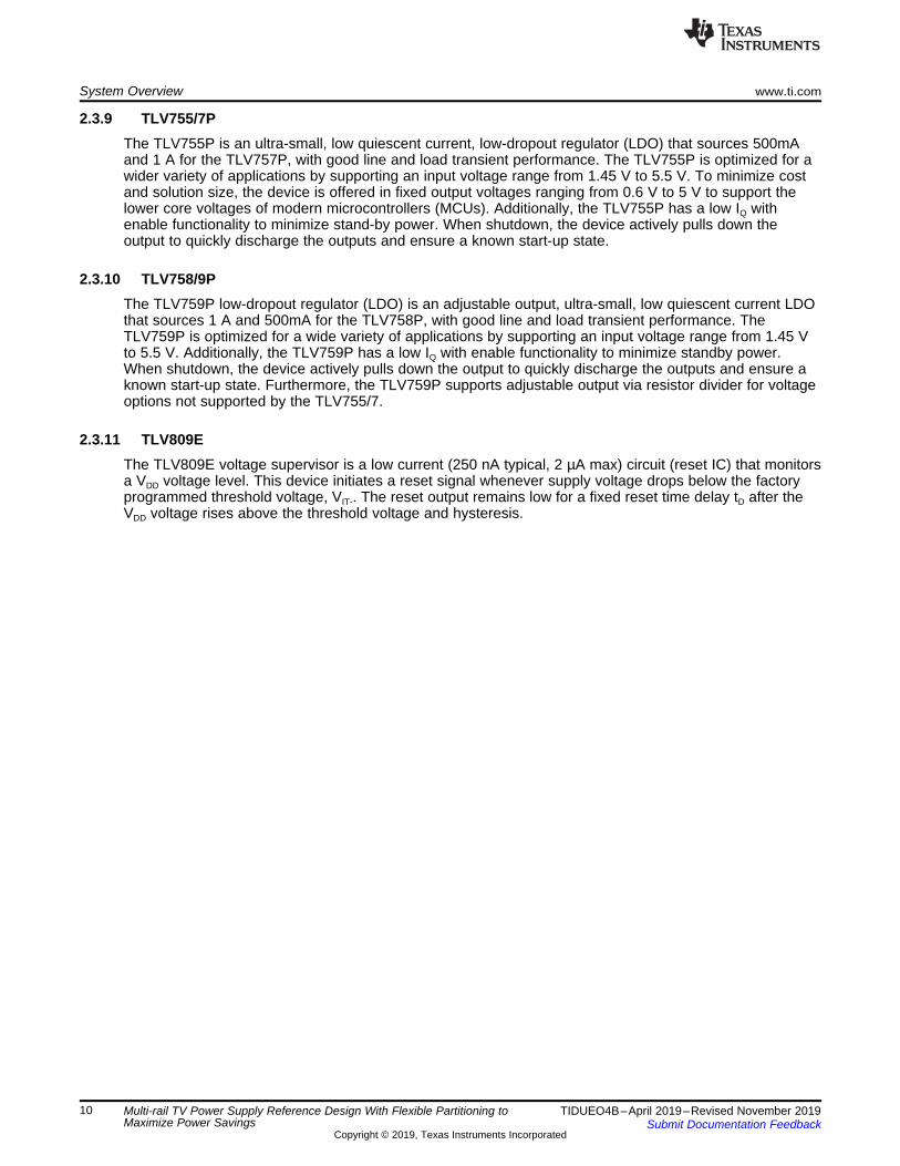
2.3.9 TLV755/7PThe TLV755P is an ultra-small, low quiescent current, low-dropout regulator (LDO) that sources 500mAand 1 A for the TLV757P, with good line and load transient performance. The TLV755P is optimized for awider variety of applications by supporting an input voltage range from 1.45 V to 5.5 V. To minimize costand solution size, the device is offered in fixed output voltages ranging from 0.6 V to 5 V to support thelower core voltages of modern microcontrollers (MCUs). Additionally, the TLV755P has a low IQ withenable functionality to minimize stand-by power. When shutdown, the device actively pulls down theoutput to quickly discharge the outputs and ensure a known start-up state.
2.3.10 TLV758/9PThe TLV759P low-dropout regulator (LDO) is an adjustable output, ultra-small, low quiescent current LDOthat sources 1 A and 500mA for the TLV758P, with good line and load transient performance. TheTLV759P is optimized for a wide variety of applications by supporting an input voltage range from 1.45 Vto 5.5 V. Additionally, the TLV759P has a low IQ with enable functionality to minimize standby power.When shutdown, the device actively pulls down the output to quickly discharge the outputs and ensure aknown start-up state. Furthermore, the TLV759P supports adjustable output via resistor divider for voltageoptions not supported by the TLV755/7.
2.3.11 TLV809EThe TLV809E voltage supervisor is a low current (250 nA typical, 2 µA max) circuit (reset IC) that monitorsa VDD voltage level. This device initiates a reset signal whenever supply voltage drops below the factoryprogrammed threshold voltage, VIT-. The reset output remains low for a fixed reset time delay tD after theVDD voltage rises above the threshold voltage and hysteresis.
www.ti.com Hardware, Software, Testing Requirements, and Test Results
11TIDUEO4B–April 2019–Revised November 2019Submit Documentation Feedback
Copyright © 2019, Texas Instruments Incorporated
Multi-rail TV Power Supply Reference Design With Flexible Partitioning toMaximize Power Savings
3 Hardware, Software, Testing Requirements, and Test Results
3.1 Required Hardware
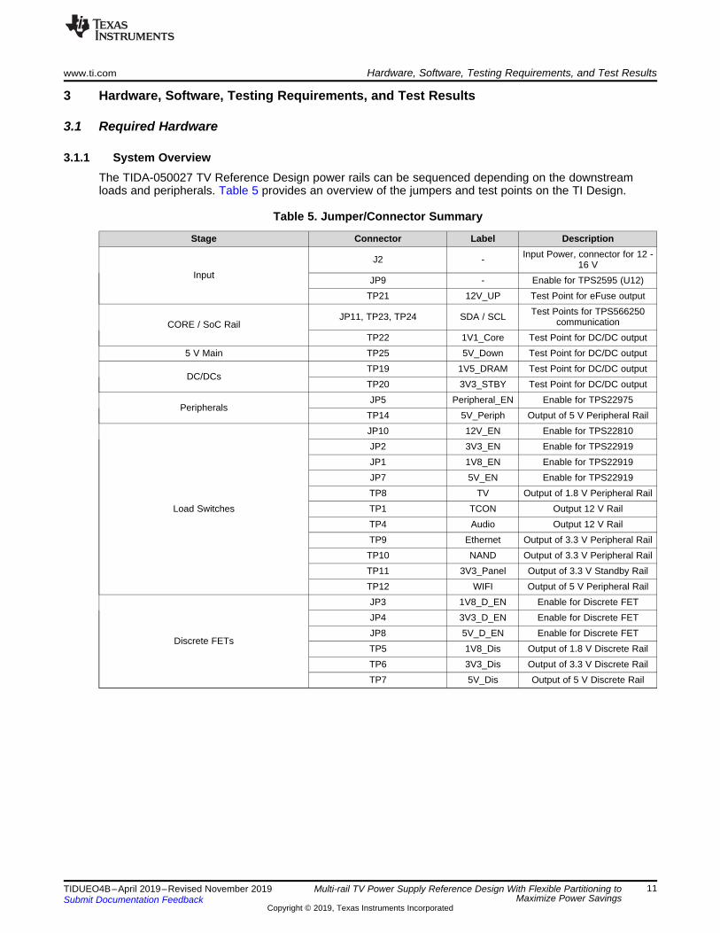
3.1.1 System OverviewThe TIDA-050027 TV Reference Design power rails can be sequenced depending on the downstreamloads and peripherals. Table 5 provides an overview of the jumpers and test points on the TI Design.
Table 5. Jumper/Connector Summary
Stage Connector Label Description
InputJ2 - Input Power, connector for 12 -
16 VJP9 - Enable for TPS2595 (U12)
TP21 12V_UP Test Point for eFuse output
CORE / SoC RailJP11, TP23, TP24 SDA / SCL Test Points for TPS566250
communicationTP22 1V1_Core Test Point for DC/DC output
5 V Main TP25 5V_Down Test Point for DC/DC output
DC/DCsTP19 1V5_DRAM Test Point for DC/DC outputTP20 3V3_STBY Test Point for DC/DC output
PeripheralsJP5 Peripheral_EN Enable for TPS22975
TP14 5V_Periph Output of 5 V Peripheral Rail
Load Switches
JP10 12V_EN Enable for TPS22810JP2 3V3_EN Enable for TPS22919JP1 1V8_EN Enable for TPS22919JP7 5V_EN Enable for TPS22919TP8 TV Output of 1.8 V Peripheral RailTP1 TCON Output 12 V RailTP4 Audio Output 12 V RailTP9 Ethernet Output of 3.3 V Peripheral RailTP10 NAND Output of 3.3 V Peripheral RailTP11 3V3_Panel Output of 3.3 V Standby RailTP12 WIFI Output of 5 V Peripheral Rail
Discrete FETs
JP3 1V8_D_EN Enable for Discrete FETJP4 3V3_D_EN Enable for Discrete FETJP8 5V_D_EN Enable for Discrete FETTP5 1V8_Dis Output of 1.8 V Discrete RailTP6 3V3_Dis Output of 3.3 V Discrete RailTP7 5V_Dis Output of 5 V Discrete Rail
Hardware, Software, Testing Requirements, and Test Results www.ti.com
12 TIDUEO4B–April 2019–Revised November 2019Submit Documentation Feedback
Copyright © 2019, Texas Instruments Incorporated
Multi-rail TV Power Supply Reference Design With Flexible Partitioning toMaximize Power Savings
3.2 Testing and Results
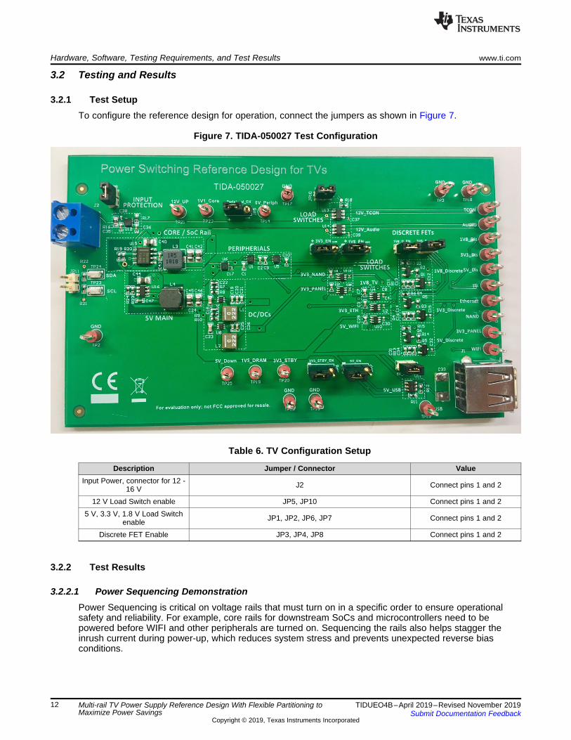
3.2.1 Test SetupTo configure the reference design for operation, connect the jumpers as shown in Figure 7.
Figure 7. TIDA-050027 Test Configuration
Table 6. TV Configuration Setup
Description Jumper / Connector ValueInput Power, connector for 12 -
16 V J2 Connect pins 1 and 2
12 V Load Switch enable JP5, JP10 Connect pins 1 and 25 V, 3.3 V, 1.8 V Load Switch
enable JP1, JP2, JP6, JP7 Connect pins 1 and 2
Discrete FET Enable JP3, JP4, JP8 Connect pins 1 and 2
3.2.2 Test Results
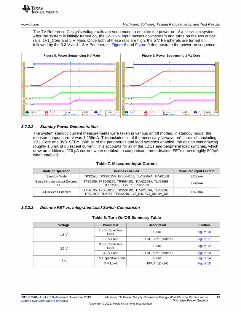
3.2.2.1 Power Sequencing DemonstrationPower Sequencing is critical on voltage rails that must turn on in a specific order to ensure operationalsafety and reliability. For example, core rails for downstream SoCs and microcontrollers need to bepowered before WIFI and other peripherals are turned on. Sequencing the rails also helps stagger theinrush current during power-up, which reduces system stress and prevents unexpected reverse biasconditions.
www.ti.com Hardware, Software, Testing Requirements, and Test Results
13TIDUEO4B–April 2019–Revised November 2019Submit Documentation Feedback
Copyright © 2019, Texas Instruments Incorporated
Multi-rail TV Power Supply Reference Design With Flexible Partitioning toMaximize Power Savings
The TV Reference Design’s voltage rails are sequenced to emulate the power-on of a television system.After the system is initially turned on, the 12 -16 V input passes downstream and turns on the two criticalrails, 1V1_Core and 5 V Main. Once both of these rails are high, the 5 V Peripherals are turned onfollowed by the 3.3 V and 1.8 V Peripherals. Figure 8 and Figure 9 demonstrate the power-on sequence.
Figure 8. Power Sequencing 5 V Main Figure 9. Power Sequencing 1 V1 Core
3.2.2.2 Standby Power DemonstrationThe system standby current measurements were taken in various on/off modes. In standby mode, themeasured input current was 1.256mA. This includes all of the necessary “always-on” core rails, including1V1_Core and 3V3_STBY. With all of the peripherals and load switches enabled, the design was drawingroughly 1.5mA of quiescent current. This accounts for all of the LDOs and peripheral load switches, whichdrew an additional 220 μA current when enabled. In comparison, three discrete FETs drew roughly 500μAwhen enabled.
Table 7. Measured Input Current
Mode of Operation Devices Enabled Measured Input CurrentStandby Mode TPS2595, TPS566250, TPS564201, TLV62569A, TLV62568 1.256mA
Everything on except DiscreteFETs
TPS2595, TPS566250, TPS564201, TLV62569A, TLV62568,TPS22975, TLV757, TPS22919 1.478mA
All Devices Enabled TPS2595, TPS566250, TPS564201, TLV62569A, TLV62568,TPS22975, TLV757, TPS22919, 1V8_Dis, 3V3_Dis, 5V_Dis 1.923mA
3.2.2.3 Discrete FET vs. Integrated Load Switch Comparison
Table 8. Turn On/Off Summary Table
Voltage Parameter Description Section
1.8 V1.8 V Capacitive
Load 100uF Figure 10
1.8 V Load 100uF, 3.6Ω (500mA) Figure 11
3.3 V3.3 V Capacitive
Load 100uF Figure 12
3.3 V Load 100uF, 5.5Ω (600mA) Figure 13
5 V5 V Capacitive Load 100uF Figure 14
5 V Load 100uF, 1Ω (1A) Figure 15
Hardware, Software, Testing Requirements, and Test Results www.ti.com
14 TIDUEO4B–April 2019–Revised November 2019Submit Documentation Feedback
Copyright © 2019, Texas Instruments Incorporated
Multi-rail TV Power Supply Reference Design With Flexible Partitioning toMaximize Power Savings
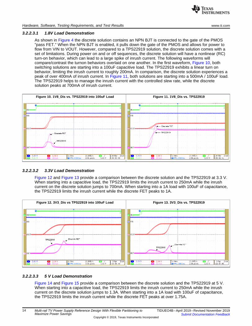
3.2.2.3.1 1.8V Load DemonstrationAs shown in Figure 4 the discrete solution contains an NPN BJT is connected to the gate of the PMOS"pass FET." When the NPN BJT is enabled, it pulls down the gate of the PMOS and allows for power toflow from VIN to VOUT. However, compared to a TPS22919 solution, the discrete solution comes with aset of limitations. During power on and or off sequences, the discrete solution will have a nonlinear (RC)turn-on behavior, which can lead to a large spike of inrush current. The following waveforms willcompare/contrast the turnon behaviors overlaid on one another. In the first waveform, Figure 10, bothswitching solutions are starting into a 100uF capacitive load. The TPS22919 exhibits a linear turn onbehavior, limiting the inrush current to roughly 200mA. In comparison, the discrete solution experiences apeak of over 400mA of inrush current. In Figure 11, both solutions are starting into a 500mA / 100uF load.The TPS22919 helps to manage the inrush current with the controlled slew rate, while the discretesolution peaks at 700mA of inrush current.
Figure 10. 1V8_Dis vs. TPS22919 into 100uF Load Figure 11. 1V8_Dis vs. TPS22919
3.2.2.3.2 3.3V Load DemonstrationFigure 12 and Figure 13 provide a comparison between the discrete solution and the TPS22919 at 3.3 V.When starting into a capacitive load, the TPS22919 limits the inrush current to 250mA while the inrushcurrent on the discrete solution jumps to 700mA. When starting into a 1A load with 100uF of capacitance,the TPS22919 limits the inrush current while the discrete FET peaks to 1A.
Figure 12. 3V3_Dis vs TPS22919 into 100uF Load Figure 13. 3V3_Dis vs. TPS22919
3.2.2.3.3 5 V Load DemonstrationFigure 14 and Figure 15 provide a comparison between the discrete solution and the TPS22919 at 5 V.When starting into a capacitive load, the TPS22919 limits the inrush current to 250mA while the inrushcurrent on the discrete solution jumps to 1.3A. When starting into a 1A load with 100uF of capacitance,the TPS22919 limits the inrush current while the discrete FET peaks at over 1.75A.
www.ti.com Hardware, Software, Testing Requirements, and Test Results
15TIDUEO4B–April 2019–Revised November 2019Submit Documentation Feedback
Copyright © 2019, Texas Instruments Incorporated
Multi-rail TV Power Supply Reference Design With Flexible Partitioning toMaximize Power Savings
Figure 14. 5V_Dis vs. TPS22919 into 100uF Load Figure 15. 5 V_Dis vs. TPS22919
3.2.2.3.4 Thermal ProtectionThermal shutdown protects the device from failure when the device junction temperature exceeds its safelimit. During operation, the junction temperature can rise due to many factors, including a high currentload, large inrush current during startup, or during a fault condition. Thermal protection turns off the switchto protect itself by reducing the power dissipation, also potentially avoiding damage to upstream anddownstream components. In comparison, a discrete FET cannot protect itself if it exceeds it’s thermaljunction temperature. In this case, the FET could potentially break, causing a short and damaging thedownstream load or peripheral.
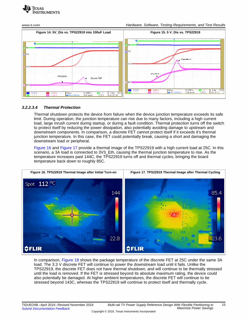
Figure 16 and Figure 17 provide a thermal image of the TPS22919 with a high current load at 25C. In thisscenario, a 3A load is connected to 3V3_Eth, causing the thermal junction temperature to rise. As thetemperature increases past 144C, the TPS22919 turns off and thermal cycles, bringing the boardtemperature back down to roughly 85C.
Figure 16. TPS22919 Thermal Image after Initial Turn-on Figure 17. TPS22919 Thermal Image after Thermal Cycling
In comparison, Figure 18 shows the package temperature of the discrete FET at 25C under the same 3Aload. The 3.3 V discrete FET will continue to power the downstream load until it fails. Unlike theTPS22919, the discrete FET does not have thermal shutdown, and will continue to be thermally stresseduntil the load is removed. If the FET is stressed beyond its absolute maximum rating, the device couldalso potentially be damaged. At higher ambient temperatures, the discrete FET will continue to bestressed beyond 143C, whereas the TPS22919 will continue to protect itself and thermally cycle.
Hardware, Software, Testing Requirements, and Test Results www.ti.com
16 TIDUEO4B–April 2019–Revised November 2019Submit Documentation Feedback
Copyright © 2019, Texas Instruments Incorporated
Multi-rail TV Power Supply Reference Design With Flexible Partitioning toMaximize Power Savings
Figure 18. Discrete FET Thermal Image
3.2.2.3.5 Transient Protection FeaturesTV Power Architectures can be stressed during startup and fault conditions. During these conditions,discrete FETs can dissipate more power that exceeds the physical and thermal limits of the MOSFET. Ifproper tests aren’t taken into consideration, the system can fail due to overstressing these components.Additionally, some of these fault conditions, such as short circuit protection and hot plug protection, areoften difficult to implement discretely and require additional components and design complexity. By usingintegrated devices on the TIDA-050027, these additional protection features can make the design morerobust while simplifying the design.
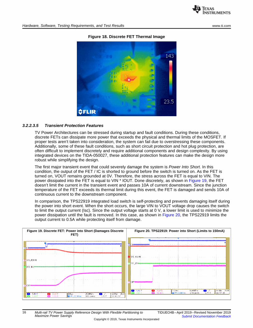
The first major transient event that could severely damage the system is Power Into Short. In thiscondition, the output of the FET / IC is shorted to ground before the switch is turned on. As the FET isturned on, VOUT remains grounded at 0V. Therefore, the stress across the FET is equal to VIN. Thepower dissipated into the FET is equal to VIN * IOUT. Done discretely, as shown in Figure 19, the FETdoesn’t limit the current in the transient event and passes 10A of current downstream. Since the junctiontemperature of the FET exceeds its thermal limit during this event, the FET is damaged and sends 10A ofcontinuous current to the downstream component.
In comparison, the TPS22919 integrated load switch is self-protecting and prevents damaging itself duringthe power into short event. When the short occurs, the large VIN to VOUT voltage drop causes the switchto limit the output current (Isc). Since the output voltage starts at 0 V, a lower limit is used to minimize thepower dissipation until the fault is removed. In this case, as shown in Figure 20, the TPS22919 limits theoutput current to 0.5A while protecting itself from damage.
Figure 19. Discrete FET: Power into Short (Damages DiscreteFET)
Figure 20. TPS22919: Power into Short (Limits to 150mA)
Load (A)
Effic
ien
cy (
%)
0.02 0.05 0.1 0.2 0.3 0.5 0.7 1 2 3 4 5 60.2
0.28
0.36
0.44
0.52
0.6
0.68
0.76
0.84
0.92
1
D003
12 V16 V
Load (A)
Eff
icie
ncy
0.020.03 0.05 0.1 0.2 0.3 0.5 0.7 1 2 3 40.6
0.64
0.68
0.72
0.76
0.8
0.84
0.88
0.92
0.96
1
D004
12 V,16 V
Load (A)
Effic
ien
cy (
%)
0.025 0.05 0.07 0.1 0.2 0.3 0.4 0.5 0.7 10.8
0.82
0.84
0.86
0.88
0.9
0.92
0.94
0.96
0.98
1
D001
5 V
Load (A)
Eff
icie
ncy (
%)
0.025 0.05 0.07 0.1 0.2 0.3 0.5 0.7 1 20.3
0.4
0.5
0.6
0.7
0.8
0.9
1
D002
www.ti.com Hardware, Software, Testing Requirements, and Test Results
17TIDUEO4B–April 2019–Revised November 2019Submit Documentation Feedback
Copyright © 2019, Texas Instruments Incorporated
Multi-rail TV Power Supply Reference Design With Flexible Partitioning toMaximize Power Savings
The other major transient event that could severely damage the system is Hot Short. In this condition, theoutput of the FET / IC is shorted to ground when the device is already turned on. This event is consideredthe more stressful event since the switch usually starts out hotter due to the pre-existing load current. Thepower dissipated into the switch is equal to VIN * IOUT. Figure 21 demonstrates a discreteimplementation. Since the discrete FET doesn’t limit the current in the transient, more than 10A passesdownstream and the FET fails.
In comparison, the TPS22919 integrated load switch measures the voltage drop across the device andlimits the output current within tsc. The device continues to limit the current until it reaches the thermalshutdown temperature. At this point, the device turns off until the junction temperature has lowered. Asshown in Figure 22 the TPS22919 limits the output current and turns off, dropping the output voltage to 0V and protecting itself from damage.
Figure 21. Discrete FET: Hot Short (Damages Discrete FET) Figure 22. TPS22919: Hot Short
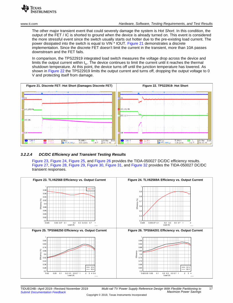
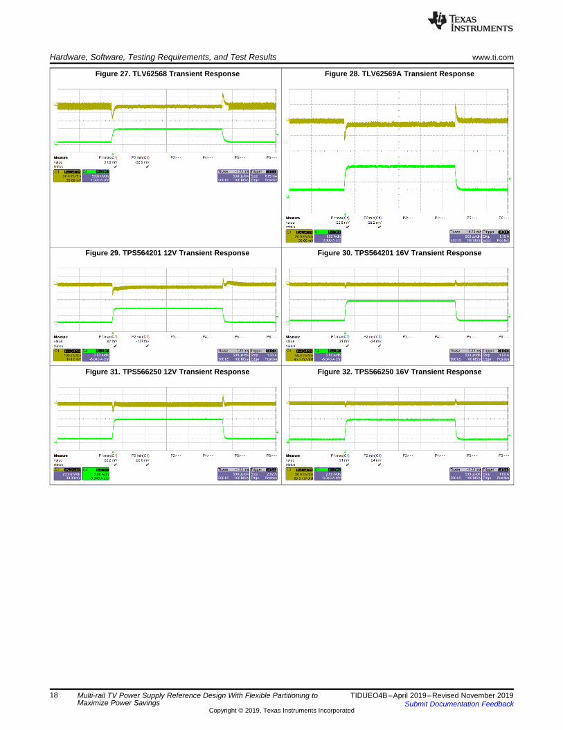
3.2.2.4 DC/DC Efficiency and Transient Testing ResultsFigure 23, Figure 24, Figure 25, and Figure 26 provides the TIDA-050027 DC/DC efficiency results.Figure 27, Figure 28, Figure 29, Figure 30, Figure 31, and Figure 32 provides the TIDA-050027 DC/DCtransient responses.
Figure 23. TLV62568 Efficiency vs. Output Current Figure 24. TLV62569A Efficiency vs. Output Current
Figure 25. TPS566250 Efficiency vs. Output Current Figure 26. TPS564201 Efficiency vs. Output Current
Hardware, Software, Testing Requirements, and Test Results www.ti.com
18 TIDUEO4B–April 2019–Revised November 2019Submit Documentation Feedback
Copyright © 2019, Texas Instruments Incorporated
Multi-rail TV Power Supply Reference Design With Flexible Partitioning toMaximize Power Savings
Figure 27. TLV62568 Transient Response Figure 28. TLV62569A Transient Response
Figure 29. TPS564201 12V Transient Response Figure 30. TPS564201 16V Transient Response
Figure 31. TPS566250 12V Transient Response Figure 32. TPS566250 16V Transient Response
www.ti.com Design Files
19TIDUEO4B–April 2019–Revised November 2019Submit Documentation Feedback
Copyright © 2019, Texas Instruments Incorporated
Multi-rail TV Power Supply Reference Design With Flexible Partitioning toMaximize Power Savings
4 Design Files
4.1 Altium ProjectTo download the Altium Designer® project files, see the design files at TIDA-050027.
4.2 SchematicsTo download the schematics, see the design files at TIDA-050027.
4.3 Bill of MaterialsTo download the bill of materials (BOM), see the design files at TIDA-050027.
4.4 PCB Layout Recommendations
4.4.1 Layout PrintsTo download the layer plots, see the design files at TIDA-050027.
4.5 Gerber FilesTo download the Gerber files, see the design files at TIDA-050027.
4.6 Assembly DrawingsTo download the assembly drawings, see the design files at TIDA-050027.
5 Software FilesTo download the software files, see the design files at TIDA-050027.
6 Related Documentation1. Integrated Load Switches versus Discrete MOSFETs app report2. Basics of Power Switches app report
6.1 TrademarksE2E is a trademark of Texas Instruments.Altium Designer is a registered trademark of Altium LLC or its affiliated companies.All other trademarks are the property of their respective owners.
6.2 Third-Party Products DisclaimerTI'S PUBLICATION OF INFORMATION REGARDING THIRD-PARTY PRODUCTS OR SERVICES DOESNOT CONSTITUTE AN ENDORSEMENT REGARDING THE SUITABILITY OF SUCH PRODUCTS ORSERVICES OR A WARRANTY, REPRESENTATION OR ENDORSEMENT OF SUCH PRODUCTS ORSERVICES, EITHER ALONE OR IN COMBINATION WITH ANY TI PRODUCT OR SERVICE.
Revision History www.ti.com
20 TIDUEO4B–April 2019–Revised November 2019Submit Documentation Feedback
Copyright © 2019, Texas Instruments Incorporated
Revision History
Revision HistoryNOTE: Page numbers for previous revisions may differ from page numbers in the current version.
Changes from A Revision (May 2019) to B Revision ...................................................................................................... Page
• Added There are two voltage supervisors on the 5 V rail from the buck converter and the LDO that monitor the rails andreset on undervoltage conditions. ....................................................................................................... 1
• Added product folder...................................................................................................................... 1• Added info on voltage supervisors. ..................................................................................................... 1• Changed diagram to include TLV809E. ................................................................................................ 1• Added TLV809E to block diagram. ..................................................................................................... 4• Added section on voltage supervisors. ................................................................................................. 8• Added new section on TLV809E. ..................................................................................................... 10
Changes from Original (May 2019) to A Revision ........................................................................................................... Page
• Changed title from Power Switching Reference Design for TVs to Multi-rail TV Power Supply Reference Design WithFlexible Partitioning to Maximize Power Savings ..................................................................................... 1
IMPORTANT NOTICE AND DISCLAIMER
TI PROVIDES TECHNICAL AND RELIABILITY DATA (INCLUDING DATASHEETS), DESIGN RESOURCES (INCLUDING REFERENCEDESIGNS), APPLICATION OR OTHER DESIGN ADVICE, WEB TOOLS, SAFETY INFORMATION, AND OTHER RESOURCES “AS IS”AND WITH ALL FAULTS, AND DISCLAIMS ALL WARRANTIES, EXPRESS AND IMPLIED, INCLUDING WITHOUT LIMITATION ANYIMPLIED WARRANTIES OF MERCHANTABILITY, FITNESS FOR A PARTICULAR PURPOSE OR NON-INFRINGEMENT OF THIRDPARTY INTELLECTUAL PROPERTY RIGHTS.These resources are intended for skilled developers designing with TI products. You are solely responsible for (1) selecting the appropriateTI products for your application, (2) designing, validating and testing your application, and (3) ensuring your application meets applicablestandards, and any other safety, security, or other requirements. These resources are subject to change without notice. TI grants youpermission to use these resources only for development of an application that uses the TI products described in the resource. Otherreproduction and display of these resources is prohibited. No license is granted to any other TI intellectual property right or to any thirdparty intellectual property right. TI disclaims responsibility for, and you will fully indemnify TI and its representatives against, any claims,damages, costs, losses, and liabilities arising out of your use of these resources.TI’s products are provided subject to TI’s Terms of Sale (www.ti.com/legal/termsofsale.html) or other applicable terms available either onti.com or provided in conjunction with such TI products. TI’s provision of these resources does not expand or otherwise alter TI’s applicablewarranties or warranty disclaimers for TI products.
Mailing Address: Texas Instruments, Post Office Box 655303, Dallas, Texas 75265Copyright © 2019, Texas Instruments Incorporated


![GUIDANCE FOR INSPECTION OF AND LEAK DETECTION IN …...ammonia rail transport [Ref 9] and inspection of atmospheric, refrigerated ammonia storage tanks [Ref 12]. Ammonia is produced](https://img.pdfslide.us/doc/110x75/5e9aa764d2b29c0edf5f25bb/guidance-for-inspection-of-and-leak-detection-in-ammonia-rail-transport-ref.jpg)