Embed Size (px)
Citation preview

MUHAMMAD UZAIR
IMPLEMENTATION OF SPACE–VECTOR-MODULATION IN A
THREE-PHASE VSI-TYPE GRID-CONNECTED INVERTER
Master of Science thesis
Examiner: Prof.Teuvo SuntioExaminer and topic approved by theFaculty Council of the Faculty ofComputing and ElectricalEngineering on 6thFeb, 2015
1
ABSTRACT
TAMPERE UNIVERSITY OF TECHNOLOGY Master’s Degree Programme in Electrical Engineering MUHAMMAD UZAIR: Implementation of space-vector-modulation in three- phase VSI-type grid-connected inverter. Master of Science Thesis, 49 pages, 13 Appendix pages September 2015 Major: Smart Grids Examiner: Professor Teuvo Suntio Keywords: SVPWM, THD, VSI, NPC, stationary vectors.
The motivation behind this thesis is to generate AC signal of varying amplitude and
frequency from a constant DC source. The device which is used to obtain this kind of
action is known as inverter. At present, the inverter is classified into three ways i.e.
square wave inverter, modified sine wave inverter or quasi sine wave inverter and pure
sine wave inverter. The first two classification of inverter have seldom used and have
very limited applications. Nowadays, the pure sine wave inverter is more demanding
because of the requirement of high efficiency and reliability. On the contrary, it is more
complex to implement. The main focus of this thesis is the implementation of space
vector-pulse-width-modulation (SVPWM) which is one of the algorithm of different
pulse-width-modulation techniques. It is applicable for three phase voltage-source-
inverter for controlling induction and synchronous machine. In this technique, the
reference vector of varying amplitude and direction continually revolve around the
hexagon with a fixed sampling frequency generating a gate pulses for the 12 power
switches used in neutral-point-converter. The space-vector-pulse-width-modulation is
advantageous over carrier based pulse-width-modulation. The properties which are used
to analyze the performance of different pulse width modulation methods are total
harmonic distortion (THD) and the amplitude of fundamental component. Better
utilization of DC bus voltage makes the space-vector-pulse-width-modulation better
than the carrier based pulse-width-modulation.
This thesis explains the concept, theory and implementation of three level space-vector
pulse-width modulation using MATLAB/Simulink environment. It also incorporates the
waveform of 7-segment, 9 segment and 13-segment switching pattern to avoid the
problem of harmonics. The concept of DC-neutral-point-potential control has also been
developed. To support the theory, gating signal pattern has been drawn and some
mathematical calculations have been performed. To get the clear picture of voltage
measurement at each output stage, the derivation of line-to-line voltages and line-to-
neutral voltages are also taken into account along with the calculation of duty cycle of
switches.

ii
PREFACE
I would like to express my sincere gratitude and thanks to my supervisor Prof. Teuvo
Suntio for giving me this precious opportunity to work under his supervision. Without
him I wouldn‟t able to achieve this goal. His guidance and kind advice filled me with
enthusiasm which helped me to achieve this milestone.
I would also like to appreciate the effort made by my true friend Mr. Umair Fatimi for
his kind assistance throughout my thesis.
Last but not least I am very much thankful to my parents and brothers for their moral
support in every stage of my entire life.
Tampere, 20.09.2015
Muhammad Uzair

iii
CONTENTS
1. INTRODUCTION .................................................................................................... 1
1.1 Background .................................................................................................... 1
1.2 Thesis outline ................................................................................................. 3
2. MODULATION STRATEGIES ............................................................................... 4
2.1 Modulation Techniques for Multilevel Inverter ............................................. 4
2.1.1 Carrier based modulation ...................................................................... 4
2.1.1.1 Two level shifted carriers .......................................................... 4
2.1.1.2 Phase shifting of level shifted carriers ...................................... 5
2.1.2 Space vector modulation ....................................................................... 7
2.2 Conclusion ...................................................................................................... 8
3. ANALYSIS OF THREE LEVEL INVERTER ........................................................ 9
3.1 Introduction .................................................................................................... 9
3.2 Concept of space vector ................................................................................. 9
3.3 Multilevel voltage source inverter................................................................ 11
3.3.1 Neutral point clamped inverter………………………………………11
3.4 Switching states ............................................................................................ 13
3.5 Space vector PWM algorithm ...................................................................... 15
3.5.1 Space vector transformation ................................................................ 15
3.5.2 Calculation of position of vector w.r.to its magnitude and direction on .
space vector plane ............................................................................... 16
3.5.3 Classification of stationary vectors ..................................................... 19
3.5.4 Sector selection ................................................................................... 21
3.5.5 Methodology for region selection ....................................................... 22
3.5.6 Dwell time calculation ........................................................................ 23
3.6 DC neutral point potential control ................................................................ 26
3.6.1 Implmentation of different switching schemes ................................... 28
3.7 Duty cycle calculation .................................................................................. 31
3.8 DC Link Current........................................................................................... 36
3.8.1 Average DC Link current over a sub-cycle ......................................... 38
3.9 Conclusion .................................................................................................... 39
3.10 Flowchart of the algorithm ........................................................................... 40
4. SIMULATION & RESULTS ................................................................................. 41
4.1 Introduction .................................................................................................. 41
4.2 Output from Clark‟s trnasformation ............................................................. 41
4.3 Sector selector .............................................................................................. 42
4.4 Region selector ............................................................................................. 43
4.5 Gating signal generator ................................................................................ 44
4.6 Model parameters ......................................................................................... 44
4.7 Line to neutral voltage with harmonic analysis ........................................... 45

iv
4.8 Line to line voltage with harmonic analysis................................................. 46
4.9 Implementation of filter ............................................................................... 47
5. CONCLUSIONS ..................................................................................................... 49
5.1 Future work proposal ................................................................................... 49
REFERENCES ................................................................................................................ 50
APPENDIX I: Implementation of conversion of three phase quantities to stationary
reference frame.
APPENDIX II: Mathematical model of “Sector selection block”.
APPENDIX III: Mathematical model of “Region selection block”.
APPENDIX IV: Mathematical model of “Dwell time calculation block”.
APPENDIX V: Analysis of Y-φ a) FFT window of Y- φ b) Harmonic analysis of Y-φ.
APPENDIX VI: Analysis of B-φ a) FFT window of B- φ b) Harmonic analysis of B-φ.
APPENDIX VII: Analysis of Y- φ current a) current waveform b) Harmonic analysis.
APPENDIX VIII: Analysis of B- φ current a) current waveform b) Harmonic analysis.
APPENDIX IX: Switching schemes for sector II, III, IV, V and VI.
APPENDIX X: a) Simulink model of 3-level inverter b) power stage of the inverter.

v
LIST OF FIGURES
Figure 1. Worst error representation of 2-level and 3-level inverter. ...................... 3
Figure 2. Level shifted carriers. ................................................................................ 5
Figure 3. Phase shifted carriersLevel shifted carriers .............................................. 5
Figure 4. Out of phase shifted carriersPhase shifted carriers. ................................. 6
Figure 5. Switching sequence of out of phase carrier ............................................... 6
Figure 6. Space vector diagram for three level inverter. .......................................... 7
Figure 7. 3-level NPC inverterSpace vector diagram for three level inverter ........ 12
Figure 8. Neutral point and DC midpoint reprsentation. ....................................... 13
Figure 9. Switching state at [+] .............................................................................. 13
Figure 10. Switching state at [0]............................................................................... 14
Figure 11. Switching state at [-] ............................................................................... 14
Figure 12. Pictorial view of clark’s transformation. ................................................ 15
Figure 13. Phasor representation of phase and line-line voltages ........................... 17
Figure 14. Space vector of 3-Level NPC ................................................................... 19
Figure 15. Sector I and all its four region. ............................................................... 22
Figure 16. View of region I of sector I ...................................................................... 22
Figure 17. Active vectors and their corresponding time in sector I, region I ........... 24
Figure 18. Small vector effects on DC neutral point a)Negative small vector
b)positive small vector ............................................................................. 26
Figure 19. 13-segment switching pattern for sector I, region I. ............................... 30
Figure 20. 7-segment switching pattern for sector I, region II ................................. 30
Figure 21. 9-segment switching pattern for sector I, region III. ............................... 31
Figure 22. 7-segment switching pattern for sector I, region IV ................................ 31
Figure 23. a) Gating signa pattern of sector I, region I. ........................................... 35
Figure 23. b) Gating signal pattern of sector I, region II. ........................................ 35
Figure 23. c) Gating signal pattern of sector I, region III. ....................................... 36
Figure 23. d) Gating signal pattern of sector I, region IV. ....................................... 36
Figure 24. DC link current and each phase leg current ........................................... 37
Figure 25. DC link current over a sub-cycle............................................................. 38
Figure 26. SVPWM algorithm representation in flow chart ..................................... 40
Figure 27. Magnitude of reference vector . .............................................................. 42
Figure 28. Angular position of reference vector ....................................................... 42
Figure 29. Output of sector determination block. ..................................................... 43
Figure 30. Output of region determination block. .................................................... 43
Figure 31. Gating signals of R-φ leg (i) 𝑆𝐴1 𝑖𝑖 𝑆𝐴1′ (iii)𝑆𝐴2(iv)𝑆𝐴2′ ......................... 44
Figure 32. 3-φ line- to- neutral voltages. .................................................................. 45
Figure 33. Analysis of R-φ voltage a) FFT window of R-phase leg b)
Harmonic profile of R-phase leg ............................................................. 46
Figure 34. Line-to-Line voltages between R-phase and Y-phase .............................. 47

vi
Figure 35. Analysis of line-to-line voltage a) FFT window of line-to-line
voltage b)Harmonic profile of line-line voltage . ................................... 47
Figure 36. Analysis of R- φ current a) R-phase current waveform b) Harmonic
profile of R-φ current a) FFT window of line-to-line voltage ................. 48

vii
LIST OF TABLES
Table 1. 3-level NPC inverter output voltage levels and their switching
states for phase A.... …………………………………………………………...12
Table 2. Status of power switches during switching states.................................... 15
Table 3. Switching schemes of stationary vectors. ................................................ 19
Table 4. Dwell time of sector I .............................................................................. 25
Table 5. Status of neutral current .......................................................................... 28
Table 6. Switching pattern of sector I.................................................................... 29

viii
LIST OF SYMBOLS AND ABBREVIATIONS
AC Alternating Current
DC Direct Current
DCMC Diode Clamped Multilevel Converter
DSP Digital Signal Processor
FCMC Flying Capacitor Multilevel Converter
IGBT Insulated Gate Bipolar Transistor
mmf Magnetomotive Force
NPC Neutral Point Converter
PWM Pulse Width Modulation
SVC Static VAR Compensator
SVG Static VAR Generator
SVPWM Space Vector Pulse Width Modulation
THD Total harmonic Distortion
UPS Uninterruptable Power Supply
VSI Voltage Source Inverter
α real axis
β imaginary axis
F magnetomotive Force
iR R-phase current
θae angle between the produced magnetic field w.r.to its axis
1 fundamental component
ω angular velocity
Vref reference voltage
m modulation index
d duty cycle
.

1
1. INTRODUCTION
1.1 Background
From the last two decades or so, the growth in the renewable energy sources has
increased tremendously which leads to increase the demand of power electronics
converter. Energy generated from renewable energy like wind, wave and photovoltaic
are heavily dependent on power converters as they are not capable of producing such
amount of power that the grid can stand with it. The power generated from these
renewable sources cannot directly connect to the grid; it needs to meet some criteria by
means of frequency, phase and amplitude. To meet the demand of grid need to
incorporate some sort of device which is capable of providing such amount of power the
grid will able to handle. Here, the role of power electronics converter comes into action.
Power electronics converter provides an intermediate role between the source of
renewable energy and grid. The PWM inverter is more demanding nowadays which is
used to convert the DC power obtained from different renewable energy sources to AC
power but the quality of power is distorted leads to total harmonic distortion which is
undesirable. In order to mitigate this problem, the multilevel inverter comes into handy
as the THD is tremendously reduced in it.
The two factors have a prominent role in order to cope with problem of harmonics.
Firstly, by means of power filters but it is cost demanding as it is made up of different
kind of metals [1]. Secondly, the fundamental component of output waveform must be
chopped off with several numbers of levels [1]. In case of three phase system, the
alternate way to get away from the problem of harmonic is to switch only one phase per
switching instant while the other two phases keep on their initial position.
The role of multilevel converters appears when total harmonic distortion (THD) has
become a significant problem which needs to mitigate in order to transfer maximum
amount of power.PWM (Pulse width modulation) is a technique through which the
ON/OFF duration of the power switch (IGBT, MOSFET) can be controlled in an
efficient manner by properly adjusting the width of the pulse. It has a prominent role in
the speed control of motor, switch mode converters etc.
The inverter is divided into two categories i.e. VSI (voltage source inverter) and CSI
(current source inverter). This thesis is concerned with the VSI so it is discussed in this
section. As the name suggests, the VSI is fed from stiff DC voltage source and convert
it into AC voltage with negligible amount of Thevenin impedance [2]. If the source is

2
not considered to be stiff, a large capacitor or a bank of capacitor is placed between the
source and the inverter [2], [3]. This DC is obtained from battery bank by connecting
several cells in series or parallel fashion or from different renewable sources. The nature
of output voltage can be varied from constant voltage to a variable voltage depending
upon the application ranging from Static VAR Generator (SVG) and compensator
(SVC), uninterruptable power supply (UPS) and AC motor drives [2]. The output
voltage produced by VSI is independent of the load.
Several types of multilevel converter have been proposed according the topological
structures which includes Diode clamped multilevel converter (DCMC), flying
capacitor multilevel converter (FCMC) and cascaded H-bridges. The other names are
also proposed for these topologies. DCMC is also regarded as Neutral point converter
(NPC). In the same fashion FCMC is also regarded as capacitor clamped converter
(CCC). DCMC is getting more popularity in industrial point of view therefore this
thesis has main focused on DCMC. The name multilevel converter is regarded for those
converters whose output carries more than 2 DC levels. Here, the phase voltages
contain 3 different DC levels so it is regarded as 3-level inverter.
The SVPWM (space vector pulse width modulation) is categorized in two ways i.e. two
level and multilevel converter. Multilevel inverter has more advantages over two level
inverter but difficult to implement due to large number of switching vectors. By
comparative analysis between the 2-level and 3-level inverter, 3-level has more power
switches i.e.12 and space vector diagram contain 27 switching vectors rather than 8
causes a less harmonic distortion. In case of 2-level inverter, the worst case error
between the applied voltage and desired voltage is quite high as compared to multi-level
inverter. As a result of this action the harmonics profile of 3-level inverter is much
better than 2-level inverter which leads to provide better waveform quality. Fig.1
represents the worst error exist between these two kinds of inverter. In case of 2-level
inverter, the desired voltage is 0.25 𝑉𝐷𝐶while the applied potentials are +0.5𝑉𝐷𝐶and
-0.5𝑉𝐷𝐶 . The duration of +0.5𝑉𝐷𝐶 is greater than -0.5𝑉𝐷𝐶 . In case of 3-level inverter, the
desired voltage is same while the applied potentials are +0.5𝑉𝐷𝐶and 0𝑉𝐷𝐶and having
same duration of being remain in conduction mode.
The challenging task is to calculate the duty cycle of each power switch [11]. The more
the level of the inverter the more the number of vectors to switch leads to provide better
quality of output in terms of harmonics and amplitude.

3
0.5Vdc
0Vdc
-0.5Vdc
0.25Vdc
Long duration
Short duration
0.5Vdc
0Vdc
0.25Vdc
-0.5Vdc
Worst case error
50% duration
50% duration
Fig.1 Worst error representation of 2-level and 3-level inverter
1.2 Thesis Outline
This thesis contains the 5 basic chapters. It begins with the introduction chapter which
contains the objective of the thesis and the need of three-level SVPWM. It also presents
the small introduction of VSI and the glimpse of comparison between two-level and
three-level inverter.
Chapter 2 has given the brief concept of different modulation strategies used in
multilevel inverter through which the duty cycle of the power switches can be
controlled in an efficient manner. The purpose of different modulation schemes is to
reduce the higher order harmonics and getting higher amplitude of fundamental
component.
Chapter 3 presents the theory, concept and background of three-level SVPWM. The
concept of voltage source inverter (VSI) along with background of NPC inverter has
been developed. The derivation of pole voltages will be done based on the selection of
particular sector and region. Vector switching times is also calculated along with duty
ratio of power switches. The role of redundant vectors to control the DC midpoint
potential control is also discussed.
In chapter 4 the simulation model for the SVPWM is designed on the basis of theory
discussed in the previous chapters. The output of region and sector selection, line to line
voltage and each phase voltage before and after incorporating the filter will be
explained. The harmonic analysis at each output stage is also incorporated.
The main conclusion drawn from the simulation and future work proposal will be
discussed in chapter 5.

4
2. MODULATION STRATEGIES
2.1 Modulation Techniques for Multilevel inverter
The purpose of modulation is to control the duration of power switches to achieve the
switching pattern by means of desired amplitude and frequency. The two common
modulation techniques available to get the gating signal sequence are carrier based
modulation and space vector modulation. This thesis is more focused on the later one
while the principle of carrier based modulation is defined a bit for comparison among
the two.
2.1.1 Carrier based modulation
In carrier based PWM, gating pulses are obtained by comparison between a high
frequency triangular carrier signal with a low frequency modulated signal. It is further
divided into two schemes i.e. two-level shifted carriers and phase shifting of level
shifted carriers for three level inverters. There is a general rule of thumb for this
particular modulation scheme, if the converter is designed for „n‟ number of voltage
levels than „n-1‟ number of triangular carriers [3] required to get the gating signal by
comparing the modulating signal with these carriers.
2.1.1.1 Two-level shifted carriers
In three level inverter there is two pair of complimentary switches so it need two high
frequency carriers operating at the same frequency and amplitude but they are level
shifted by means of amplitude. Fig.2, shows the three modulating signal compared with
two triangular carriers. One carrier is running between 0V and 1V while the other
carrier is running between 0V and -1V, both carriers have same amplitude and
frequency.
Switching logic
For simplicity, the upper carrier is regarded as carrier 1 while the bottom carrier is
regarded as carrier 2. R-phase is plotted in black, Y-phase in red while B-phase in blue.
Considering the R-phase only,
When R-phase> carrier 1 and R-phase> carrier 2 yields 0.5VDC pole voltage.
When R-phase< carrier 1 and R-phase< carrier 2 yields -0.5VDC pole voltage.
5
When R-phase> carrier 1 and R-phase< carrier 2 yields 0VDC pole voltage.
Same is applied for Y and B phase.
Figure 2 Level shifted carriers
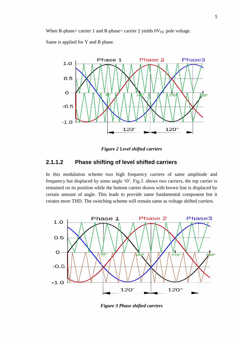
2.1.1.2 Phase shifting of level shifted carriers
In this modulation scheme two high frequency carriers of same amplitude and
frequency but displaced by some angle „Ɵ‟. Fig.3. shows two carriers, the top carrier is
remained on its position while the bottom carrier drawn with brown line is displaced by
certain amount of angle. This leads to provide same fundamental component but it
creates more THD. The switching scheme will remain same as voltage shifted carriers.
Figure 3 Phase shifted carriers

6
Figure 4 Out of phase shifted carriers
Fig.5 shows the switching sequence of two out of phase shifted carriers
diagrammatically. Here, mR, mY and mB are the three modulating signal. 1, 0 and -1
are the three conditions of power switches of NPC.
1= Top two switches are ON in each phase causes 0.5VDC at the pole.
0= Middle two switches are ON in each phase causes 0VDC at pole.
-1= Bottom two switches are ON in each phase causes -0.5VDC at pole.
1
0
-1
mR
mY
mB
RYB
+ ++ 0
- 0 00
- - - 0
Figure 5 Switching sequence of out of phase carrier

7
2.1.2 Space Vector Modulation
Space vector modulation (SVM) is a modulation technique used to create PWM pulses.
It is more extensive and computational technique among the industrial drive application
[4]. It is more demanding due to easier digital implementation on DSP controller [9]
and provides better conversion of DC into AC. It comprises of different switching
vectors with different magnitude and angle. Each switching state defines the different
output state which is obtained by combination of different stationary vector. SVM is
based on the conversion of three phase quantities to 2-dimensional plane. A plane has
always two-coordinate system. The name stationary reveals from the fact that it is
remained in stationary position in space. The bunch of these vectors combine together
to form space vector diagram. It indicates the position of each vector in space with
respect to its magnitude and angle and the reference vector rotates with constant
switching frequency within the hexagon. At each switching instant some mathematical
calculations were performed to get the PWM pulses. When the reference vector rotate
within the hexagon the inverter will operate in under modulation region or linear
provide a smooth waveform at the output terminal. In this region the inverter transfer
characteristics are naturally linear [2]. The over modulation region or non-linear region
occur when the reference vector outside the premises of hexagon.
The space vector diagram for a three level inverter is shown below,
Figure 6 Space vector diagram for three-level inverter

8
Features of SVM
Less harmonic distortion causes a minimal switching loss.
Easy to implement on DSP controllers and microprocessor [8].
Proper DC bus utilization [9].
Required complex mathematical calculation.
2.2 Conclusion
In order to connect the output produce by the converter to the electric grid, it must be
synchronized with the grid properties such as frequency, phase and amplitude. These
properties must closely resemble to the sinusoidal wave. To get this kind of wave
obtained from separate DC source, the inverter must be incorporated between the DC
source and electric grid. The switches must be ON/OFF in a predefined manner which
can be done by different modulation strategies. Here in this chapter different
modulation strategies have been discussed. By comparative analysis between these two
modulation strategies, SVPWM carries approximately 15% better utilization of voltages
[22]. The overview of sine pulse width modulation (SPWM) has given just only for
reference while the concept behind the SVPWM is further discussed in detail in the next
two chapters.

9
3. ANALYSIS OF THREE LEVEL INVERTER
3.1 Introduction
The term ”space” comes from the fact that it is composed of two dimensional plane i.e.
real plane ‟α‟ and imaginary plane ‟β‟. In order to avoid more complex calculation of
three phase system, the three phase quantities are transformed to two phase quantities
using Clark‟s transformation.
3.2 Concept of Space Vector
The concept of space vector emerged from the theory of three phase electrical machines
i.e. induction machines and synchronous machines. All of these machines comes up
with a three set of stator windings with each winding is separated from each other by an
angle of 120o. When these windings are connected to three phase AC source produces a
magnetic flux. This associated flux causes a production of magnetomotive force (mmf)
when ampere-turns setup by magnetic flux which rotate in the air gap with certain
angular frequency ‟ω‟. When this flux is linked with rotor bars causes a rotor to rotate
with synchronous speed ‟NS‟. This revolving mmf is an example of space vector.
Mathematically the pulsating magnetic field produced by a single phase winding,
,1 Cos( )R R aeF Ki (1)
where,
F= mmf produced in the air-gap
iR = rotor current
1 = fundamental component of revolving mmf
θae= angle between the produced magnetic field with respect to its axis.
Since this current is sinusoidal in nature as it is taking from AC source. So,
Cos( )R mi I t (2)
By substituting eq. (2) in eq. (1) we get,

10
,1 Cos( )Cos( )R m aeF KI t
By applying product rule of cosine function gives,
,1 Cos Cos2
mR ae ae
KIF t t (3)
From the above equation it can easily be deduced that the pulsating magnetic field is
resolved into components i.e. one rotates clockwise while the other rotates in
anticlockwise direction.
Now extend this concept to a three phase winding. The three phase current can be
written as,
CosR mi I t Cos 120Y mi I t Cos 120B mi I t
,1 CosR R aeI Ki
Similarly,
,1 Cos 120Y Y aeI Ki ,1 Cos 120B B aeI Ki
which than produce a m.m.f as given below,
,1 Cos( )R R aeF Ki (4)
,1 Cos( 120 )o
Y Y aeF Ki (5)
,1 Cos( 240 )o
B B aeF Ki (6)
By substituting the three phase current in above equation gives,
,1 max Cos( )Cos( )R aeF F t (7)
,1 max Cos( 120 )Cos( 120 )o o
Y aeF F t (8)
,1 max Cos( 240 )Cos( 240 )o o
B aeF F t (9)
where,
max * mF K I
By using trigonometric identities the equation (7) to (9) gives,

11
max,1 Cos Cos
2R ae ae
FF t t (10)
max,1 Cos Cos 240
2
o
Y ae ae
FF t t
Also can be written as,
max,1 Cos Cos 120
2
o
Y ae ae
FF t t
(11)
max,1 Cos Cos 480
2
o
B ae ae
FF t t
Also can be written as,
max,1 Cos Cos 240
2
o
B ae ae
FF t t
(12)
The average value can be computed as,
,1ag R Y B R Y BF F F F F F F
From the above equation the vector which revolves in anti-clockwise direction gets
cancelled gives,
max,1 3 Cos
2ag ae
FF t (13)
This is the vector which revolves in the air gap between stator and rotor with angular
speed (ω).
3.3 Multilevel Voltage Source Inverter
3.3.1 Neutral-Point-Clamped Inverter
There is a variety of multilevel converters available like cascaded H-Bridge inverter,
flying capacitor inverter. Each converter has its own advantage depending upon the
application but neutral-point-clamped inverter has gained more popularity and attention
as far as this thesis is concerned. If the output voltage level and power level of PWM
increased, the devices need to be connected in series gives a formation of NPC inverter
[10]. It is also named as “Diode Clamped multilevel inverter” because the diodes are
used to clamped the potential at DC mid-point „o‟ to the switching elements. A simple
configuration of three levels NPC inverter is shown in Fig.7. In general, for n-level
12
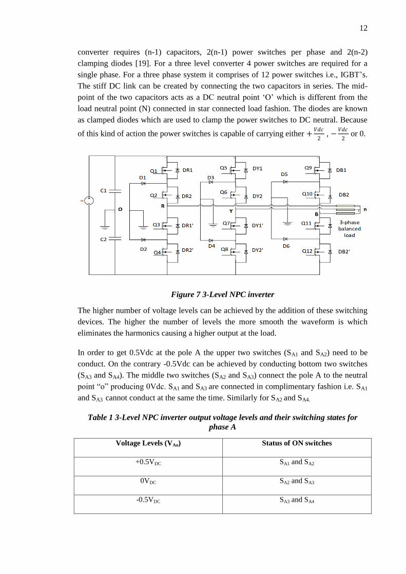
converter requires (n-1) capacitors, 2(n-1) power switches per phase and 2(n-2)
clamping diodes [19]. For a three level converter 4 power switches are required for a
single phase. For a three phase system it comprises of 12 power switches i.e., IGBT‟s.
The stiff DC link can be created by connecting the two capacitors in series. The mid-
point of the two capacitors acts as a DC neutral point „O‟ which is different from the
load neutral point (N) connected in star connected load fashion. The diodes are known
as clamped diodes which are used to clamp the power switches to DC neutral. Because
of this kind of action the power switches is capable of carrying either +𝑉𝑑𝑐
2 , −
𝑉𝑑𝑐
2 or 0.
Figure 7 3-Level NPC inverter
The higher number of voltage levels can be achieved by the addition of these switching
devices. The higher the number of levels the more smooth the waveform is which
eliminates the harmonics causing a higher output at the load.
In order to get 0.5Vdc at the pole A the upper two switches (SA1 and SA2) need to be
conduct. On the contrary -0.5Vdc can be achieved by conducting bottom two switches
(SA3 and SA4). The middle two switches (SA2 and SA3) connect the pole A to the neutral
point “o” producing 0Vdc. SA1 and SA3 are connected in complimentary fashion i.e. SA1
and SA3 cannot conduct at the same the time. Similarly for SA2 and SA4.
Table 1 3-Level NPC inverter output voltage levels and their switching states for
phase A
Voltage Levels (VAo) Status of ON switches
+0.5VDC SA1 and SA2
0VDC SA2 and SA3
-0.5VDC SA3 and SA4

13
3.4 SWITCHING STATES
In a three level inverter load neutral is different from DC mid-point „o‟. The phase
voltage is measured from the pole of each leg to the DC mid-point „o‟ while the line
voltage is measured as the difference between two poles. The switching states represent
the operating point of the power switch. For a three level inverter the switching state of
each switch is represented as either „+‟, „0‟, „-„.
Figure 8 Neutral point and DC point representation
[+] State
During the operation of this state the upper two switches of each leg of the inverter
are ON which makes the two clamping diodes are reverse biased for a certain
duration of time causes positive DC bus voltage appears across the output of each
pole while the two bottom switches are at OFF position.In this state the output is 𝑉𝑑𝑐
2.
S1
S2
S3
S4
C1
C2
Figure 9 Switching state at [+]

14
[0] State
During the operation of this state the middle switches of each leg of the inverter is
turned ON causes the clamping diodes forward biased makes a direct connection
between the output to the DC midpoint „o‟. In this state the direction of current is
dependent on the load. In this state the output is 0 Vdc.
DC
S1
S2
S3
S4
C1
C2
Figure 10 Switching state at [0]
[-] State
During the operation of this state the bottom two switches of each leg of the inverter are
ON which makes the two clamping diodes are reverse biased for a certain duration of
time causes negative DC bus voltage appears across the output of each pole while the
two top switches are at OFF position.In this state the output is -𝑉𝑑𝑐
2.
DC
C1
C2
S1
S2
S3
S4
Figure 11 Switching state at [-]

15
Table 2 Status of power switches during switching states [16]
State S1 S2 S3 S4 Pole Voltage
[+] ON ON OFF OFF 𝑉𝐷𝐶
2
[0] OFF ON ON OFF 0𝑉𝐷𝐶
[-] OFF OFF ON ON −
𝑉𝐷𝐶
2
3.5 SPACE VECTOR PWM ALGORITHM
This section describes the fundamental concept of space vector modulation which
involves the mathematical calculation of 𝑉𝛼 and 𝑉𝛽 at different switching state, dwell
time calculation of stationary vectors, criteria for the selection of region and sector and
sequence of 7-segments, 9-segments and 13-segments switching vector scheme.
3.5.1 SPACE VECTOR TRANSFORMATION
The mmf produced in a three phase winding can also be produced by a two phase
fictitious winding as well but these two winding should be separated in space by 90o
apart.
Figure 12 Pictorial view of Clark’s transformation [5]
Resolve the three phase quantities „R‟,‟Y‟ and „B‟ into equivalent two phase
components as follows,
Cos120 Cos 240
Cos30 Cos150
o o
R Y B
o o
Y B
Ni Ni Ni Ni
Ni Ni Ni
There is no component of R-phase in the direction of „β‟ axis.

16
By cancelling the common terms in above two equations gives,
Cos120 Cos 240o o
R Y Bi i i i → 2 2
Y BR
i ii i
1
2R Y Bi i i i (14)
By applying Kirchhoff current law,
0R Y Bi i i
1
2R Ri i i →
3
2Ri i (15)
Cos 30 Cos 150o o
Y Bi i i → 3
2Y Bi i i (16)
The eq. (15) and eq. (16) can also written in matrix form,
𝑖𝛼𝑖𝛽
=
3
20 0
0 3
2
− 3
2
𝑖𝑅𝑖𝑌𝑖𝐵
For a 3-φ balanced star connected load,
𝑉𝛼𝑉𝛽
=
3
20 0
0 3
2
− 3
2
𝑉𝑅
𝑉𝑌
𝑉𝐵
The magnitude of the reference vector can be calculated by,
𝑉𝑟𝑒𝑓 = 𝑉𝛼2 + 𝑉𝛽
2
The direction of the reference vector can be computed as,
Ɵ= 𝑡𝑎𝑛−1 𝑉𝛽
𝑉𝛼
3.5.2 Calculation of position of vectors with respect to its
magnitude and direction on space vector plane
Since VRO(avg), VYO(avg), VBO(avg) are available in sinusoidal quantities so they can easily
represent in phasor form. The 3-phase voltages and their corresponding line-line
voltages are given in Fig.13.

17
Vro
Vbo
Vyo
Vry
Vyb
Vbr
30
120
Figure 13 Phasor-representation of phase and line-line voltages
For instance consider the switching state [+--] which means the two top switches of R-
leg are turned ON and the bottom two switches of Y-leg & B-leg are turned ON.
For 3-φ star connected balance load,
3
RY BRRN
V VV
where,
RY RO YOV V V
2 2
DC DCRY
V VV
→ RY DCV V
BR BO ROV V V
2 2
DC DCBR
V VV
→ BR DCV V
3
DC DCRN
V VV
→
2
3
DCRN
VV
3
2RNV V which gives us,

18
DCV V (17)
3
2YN BNV V V
3
YB RYYN
V VV
1
3YN DCV V
and
1
3BN DCV V
0V (18)
The magnitude of stationary vector become,
𝑉𝑟𝑒𝑓 = 𝑉𝐷𝐶2 + 0 → 𝑉𝑟𝑒𝑓 = 𝑉𝐷𝐶
The direction of stationary vector becomes,
Ɵ= 𝑡𝑎𝑛−1 0
𝑉𝐷𝐶 → Ɵ = 0
o
which constitutes a vectorV5 in space vector plane. The corresponding 27 vectors are
formed in the same way.
6 vectors out of 27 vectors having same magnitude of 𝑉𝐷𝐶 with 60o degrees
apart. These vectors are V5 [+--], V9 [++-], V11 [-+-], V17 [-++], V21 [--+] andV25
[+-+].
12 vectors out of 27 vectors are having a same magnitude of 𝑉𝐷𝐶
2 and each two
vectors are placed at 60o degrees apart. These vectors include V3 [+00] and V4
[0--], V7 [++0] and V8 [00-], V12 [010] and V13 [-0-], V14 [0++] and V15 [-00],
V19 [00+] and V20 [- -0], V23 [+0+] and V24 [0-0].
6 vectors out of 27 vectors having same magnitude of 3
2 VDC with 60
o degrees
apart but first vector lies at 30o. These vectors are V6 [+0-], V10 [0+-], V16 [-+0],
V18 [-0+], V22 [0-+] andV26 [+-0].
The remaining 3 vectors are known as zero vectors having amplitude of 0 VDC
and an angle 00.

19
3.5.3 Classification of Stationary Vectors
The three level SVPWM composed of 27 stationary vectors (V1-V27). They are further
classified into four groups on the basis of their magnitude. The zero vectors corresponds
to those vectors whose magnitude is 0VDC. These small vectors having an amplitude of
1
2VDC. For medium vectors the amplitude is
3
2VDC. The last group of stationary vectors
is known as large vectors whose amplitude is VDC. These group combine together to
form space vectors as shown in fig.14. Table 3 represents the classification of vectors
with its amplitude.
Figure 14 Space vector of three level NPC
Table 3 Switching schemes of stationary vectors
Vector Switching State Vector
Classification
Magnitude
𝑉1 000 Zero Vector 0 𝑉𝐷𝐶
𝑉2 --- Zero Vector 0 𝑉𝐷𝐶

20
𝑉3 +00 Small Vector 1
2 𝑉𝐷𝐶
𝑉4 0- Small Vector 1
2 𝑉𝐷𝐶
𝑉5 +-- Large Vector 𝑉𝐷𝐶
𝑉6 +0- Medium Vector 3
2 𝑉𝐷𝐶
𝑉7 ++0 Small Vector 1
2 𝑉𝐷𝐶
𝑉8 00- Small Vector 1
2 𝑉𝐷𝐶
𝑉9 ++- Large Vector 𝑉𝐷𝐶
𝑉10 0+- Medium Vector 3
2 𝑉𝐷𝐶
𝑉11 -+- Large Vector 𝑉𝐷𝐶
𝑉12 0+0 Small Vector 1
2 𝑉𝐷𝐶
𝑉13 -0- Small Vector 1
2 𝑉𝐷𝐶
𝑉14 0++ Small Vector 1
2 𝑉𝐷𝐶
𝑉15 -00 Small Vector 1
2 𝑉𝐷𝐶
𝑉16 -+0 Medium Vector 3
2 𝑉𝐷𝐶
𝑉17 -++ Large Vector 𝑉𝐷𝐶
𝑉18 -0+ Medium Vector 3
2 𝑉𝐷𝐶
𝑉19 00+ Small Vector 1
2 𝑉𝐷𝐶
𝑉20 --0 Small Vector 1
2 𝑉𝐷𝐶

21
𝑉21 --+ Large Vector 𝑉𝐷𝐶
𝑉22 0-+ Medium Vector 3
2 𝑉𝐷𝐶
𝑉23 +0+ Small Vector 1
2 𝑉𝐷𝐶
𝑉24 0-0 Small Vector 1
2 𝑉𝐷𝐶
𝑉25 +-+ Large Vector 𝑉𝐷𝐶
𝑉26 +-0 Medium Vector 3
2 𝑉𝐷𝐶
𝑉27 +++ Zero Vector 0 𝑉𝐷𝐶
Furthermore, these groups of vector fall in two groups of state i.e. active state and null
state.
The null state corresponds to the condition when there is no power flow take place from
DC side to AC side. In this state (IDC=0A). It is also known as zero state and
corresponding vectors are known as zero vectors. The zero vector group lie in this state.
Whereas, active state is a state at which there is a transfer of power takes place between
DC side and AC side and corresponding vectors are known as active vectors. Large
vectors, medium vectors and small vectors are a part of this state.
3.5.4 Sectors selection
The space vector of three level inverter is divided into 6 sectors. Each sector comprise
of 60o which makes the reference vector (𝑉𝑟𝑒𝑓 ) to rotate around 360
o. Each sector is
further divided into 4 regions. So, the space vector plane is split into 6*4=24 regions.
The sector is classified on the basis of angle.
0o ≤ Ɵ < 60
o reference vector (𝑉𝑟𝑒𝑓 ) lies in Sector 1.
60o ≤ Ɵ < 120
o reference vector (𝑉𝑟𝑒𝑓 ) lies in Sector 2.
120o ≤ Ɵ < 180
o reference vector (𝑉𝑟𝑒𝑓 ) lies in Sector 3.
180o ≤ Ɵ < 240
o reference vector (𝑉𝑟𝑒𝑓 ) lies in Sector 4.
240o ≤ Ɵ < 300
o reference vector (𝑉𝑟𝑒𝑓 ) lies in Sector 5.
300o ≤ Ɵ < 360
o reference vector (𝑉𝑟𝑒𝑓 ) lies in Sector 6.

22
1 23
4
X2
X1
θ
Reference vector
Figure 15 Sector I and all its four region
3.5.5 Methodology for region selection
The region selection is done by splitting the reference vector (Vref) into its coordinates
i.e. α and β.
Figure 16 View of sector I, region I
Calculation of X2
Sin3
b
a
→
Sin3
ba
From fig.16, Sinnb X and 2a X

23
2
Sin
Sin3
nXX
→ 2
2Sin
3nX X
Calculation of X1:
1d X c
or 1CosnX X c
or 1 CosnX X c (19)
Cos3
c
a
→ 1
2c a
From the above fig. a= X2
2 1Sin
23nc X
→ Sin
3
nXc
(20)
After putting eq. (20) in eq. (19)
1
SinCos
3
nn
XX X
→ 1
Sin(Cos )
3nX X
If X1<0.5VDC, X2<0.5VDC and (X1+X2) <0.5VDC the reference vector lies in
region I.
If X1>0.5VDC the reference vector lies in region II.
If X1<0.5VDC, X2<0.5VDC and (X1+X2) >0.5VDC the reference vector lies in
region III.
If X2>0.5VDC the reference vector lies in region IV.
3.5.6 Dwell time calculation
This section describes the concept of dwell time calculation of the three nearest vector
in any region by applying the simple concept of volt-second balance which states that
“the sum of the product of voltages of space vector and duration for which these
voltages applied must equal to the product of reference voltage (Vref) and sampling
time (Ts)”. It simply means for how much time the active vectors gets conduct. The
sampling time for each switching state is „Ts‟ second and each region is split into „Ta‟,
„Tb‟ and „Tc‟ second which is the time taken by stationary vectors to remain conduct
for that duration.
24
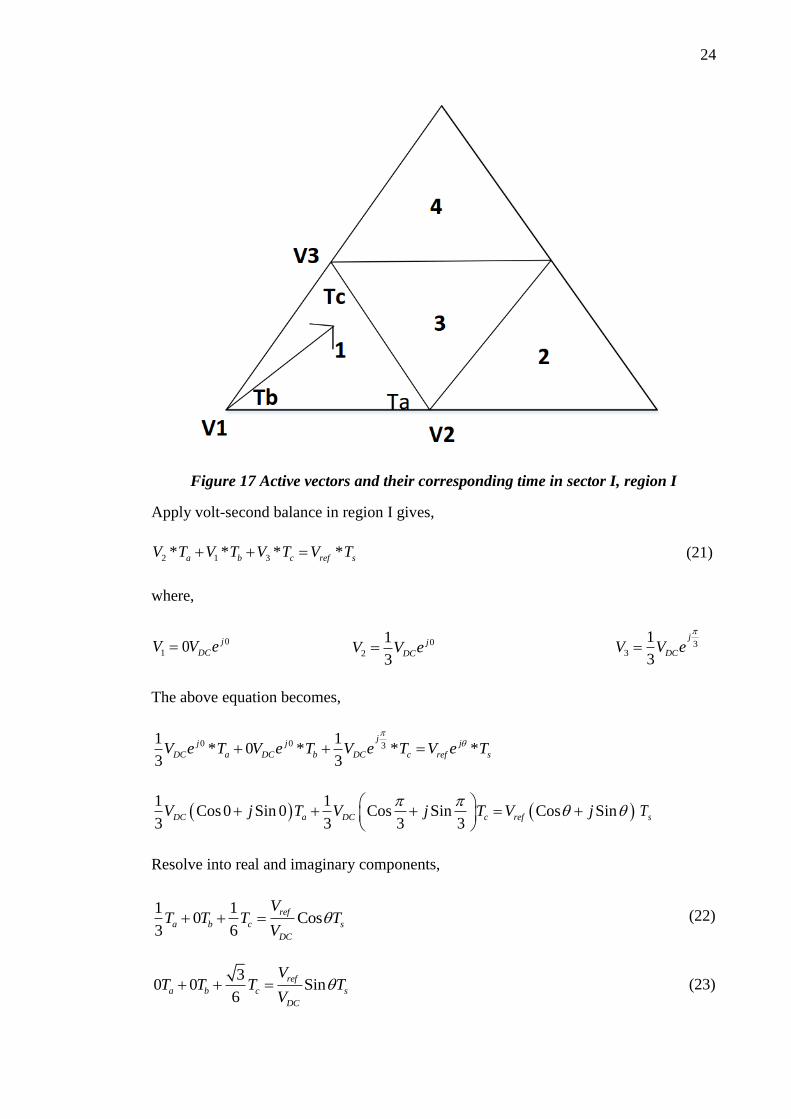
Figure 17 Active vectors and their corresponding time in sector I, region I
Apply volt-second balance in region I gives,
2 1 3* * * *a b c ref sV T V T V T V T (21)
where,
0
1 0 j
DCV V e 0
2
1
3
j
DCV V e 33
1
3
j
DCV V e
The above equation becomes,
0 0 31 1
* 0 * * *3 3
jj j j
DC a DC b DC c ref sV e T V e T V e T V e T
1 1
Cos0 Sin 0 Cos Sin Cos Sin3 3 3 3
DC a DC c refV j T V j T V j
sT
Resolve into real and imaginary components,
1 10 Cos
3 6
ref
a b c s
DC
VT T T T
V (22)
30 0 Sin
6
ref
a b c s
DC
VT T T T
V (23)

25
a b c sT T T T (24)
From eq. (23),
3 6Sin
3 3
ref
c s
DC
VT T
V
→ 2 Sinc a sT m T
where,
ma= modulation index =
By substituting value of Tc in eq. (22) gives,
33 Cos Sin
3
ref ref
a s s
DC DC
V VT T T
V V
2 Sin3
a sT T m
By substituting values of Ta and Tc in eq. (24) gives,
1 2 Sin3
b sT T m
Here are the derived values of dwell times of sector I and region I for Ɵ varies from 0
to𝜋
3.
The dwell time calculation for the remaining sectors and their corresponding region is
done in the same way.
Table 4 Dwell time for sector I
Region Ta Tb Tc
1 Ts 2𝑚 sin 𝜋
3− Ɵ Ts 1 − 2𝑚 sin
𝜋
3+ Ɵ 2msin ƟTs
2 Ts 2 − 2𝑚 sin 𝜋
3+
Ɵ
2msin ƟTs Ts 2𝑚 sin 𝜋
3− Ɵ −
1
3 1 − 2m sin Ɵ Ts Ts 2𝑚 sin 𝜋
3+ Ɵ −
1
Ts 1 − 2𝑚 sin 𝜋
3− Ɵ

26
4 2m sin Ɵ − 1 Ts Ts 2𝑚 sin 𝜋
3− Ɵ Ts 2 − 2𝑚 sin
𝜋
3+ Ɵ
The dwell time calculation for sector II to sector VI is also achieved by shifting these
sectors to sector I. Since each sector is last long for 𝜋
3 radian and resulted angle is
achieved by subtracting the multiple of 𝜋
3 from calculated angular displacement „Ɵ‟ [6].
3.6 DC Neutral Point Potential Control
The whole space vector diagram is split into 4 different groups of vectors, they are
classified as Large vectors (+--, ++-, -+-, -++, --+, +-+), Zero vectors (+++, ---, 000),
Small vectors (+00, 0--, 00-, ++0, -0-, 0+0, -00, 0++, --0, 00+, +0+, 0-0) and Medium
vectors (+0-, 0+-, -+0, -0+, 0-+, +-0). In large vectors the three phase leg are either
connected to positive rail or negative rail so they have no impact on DC neutral point.
Zero vectors short circuits the load to either positive rail, negative rail or midpoint of
the capacitors [13]. The neutral point potential is also independent of this group of
vector. In medium vector, one of the three phase is connected to neutral point and the
remaining two phase legs are connected to +ve and –ve rail respectively. So in this case
the neutral point potential deviates from zero. In small vector group, one or two phase is
always connected to the DC midpoint while the remaining phase leg is connected to
either +ve rail or –ve rail. The direction of neutral current depends on the nature of load
current. Either the load current will inject into or extract from the neutral point. It also
has an impact on the variation of DC potential. The small vector is further classified
into positive small vector or negative small vector. The positive small vector is obtained
when load current charges the upper capacitor and discharges the lower capacitor. The
vice versa is responsible for the creation of negative small vector. These two vectors are
drawn in fig.18.
a) b)
Figure 18 Small vector effects on DC neutral point a) negative small vector (0--)
b) positive small vector (+00)

27
From the basic circuit theory,
1 2o C Ci i i (25)
where,
1
1 1
C
C
dui C
dt and 2
2 2
C
C
dui C
dt
1 2
DCC o
uu u and
2 2
DCC o
uu u
The two capacitors should be match to each other gives,
1 2C C C
2 2DC DC
o o
o
u ud u d u
i c cdt dt
2 2DC DC
o o
o
u ud u u
i cdt
→ 2 o
o
d ui c
dt
2
o odu i
dt C (26)
Form the above equation it is deduce that the neutral current (𝑖𝑜) is dependent on neutral
point potential (𝑢𝑜 ).
The small vector has a redundant vector while remaining vector doesn‟t. These two
redundant vectors have same amplitude but the direction of current flow is opposite
causing a cancelling effect at the neutral point makes the neutral point potential stable.
These two redundant vectors are used to control the neutral point potential. The duty
cycle of positive and negative small vectors are combined together to get the total duty
cycle of small vector [21].
𝑑𝑠= 𝑑𝑠,𝑝 + 𝑑𝑠,𝑛
Where,
𝑑𝑠= duty cycle of small vector
𝑑𝑠,𝑝= duty cycle of positive small vector

28
𝑑𝑠,𝑛= duty cycle of negative small vector
By proper adjusting the duty cycle of these two redundant vectors the neutral point will
be stable. Table 5 shows the state of neutral current when medium and small vectors are
applied.
Table 5 Status of neutral current
Small
Vector
Neutral
current
Small
Vector
Neutral
current
Medium
Vector
Neutral
current
+00 −𝑖𝑎 -00 −𝑖𝑎 +0- 𝑖𝑏
0-- 𝑖𝑎 0++ 𝑖𝑎 0+- 𝑖𝑎
00- −𝑖𝑐 --0 𝑖𝑐 -+0 𝑖𝑐
++0 𝑖𝑐 00+ −𝑖𝑐 -0+ 𝑖𝑏
-0- 𝑖𝑏 +0+ 𝑖𝑏 0-+ 𝑖𝑎
0+0 −𝑖𝑏 0-0 −𝑖𝑏 +-0 𝑖𝑐
Consider the region I of sector I for one complete cycle, 𝑉4 (0--) and 𝑉8(00-) must be
switched during half cycle and for the next half cycle the 𝑉3(+00) and 𝑉7(++0).
𝑉4injects𝑖𝑎 current and 𝑉3 extract −𝑖𝑎 current. Similarly 𝑉7 injects 𝑖𝑐 current and 𝑉8
extract −𝑖𝑐 current.
𝑖𝑁𝑃1 = 𝑑4𝑉4 + 𝑑8𝑉8 → 𝑖𝑁𝑃1 = 𝑑4 𝑖𝑎 + 𝑑8 −𝑖𝑐
𝑖𝑁𝑃2 = 𝑑3𝑉3 + 𝑑7𝑉7 → 𝑖𝑁𝑃2 = 𝑑3 −𝑖𝑎 + 𝑑7 𝑖𝑐
𝑖𝑜= 𝑖𝑁𝑃1 + 𝑖𝑁𝑃2 = 0
where d3, d4, d7 and d8 are the duty cycles of the corresponding vector.
While keep this into mind, the available switching schemes are discussed in next
section.
3.6.1 Implementation of different switching scheme
This section describes the need of different switching schemes i.e. 7-segment switching
scheme, 9-segment switching scheme and 13-segment switching scheme which

29
incorporates the switching of one phase at a time to mitigate the problem of harmonics.
The waveform of these switching segments will be drawn in support of this statement.
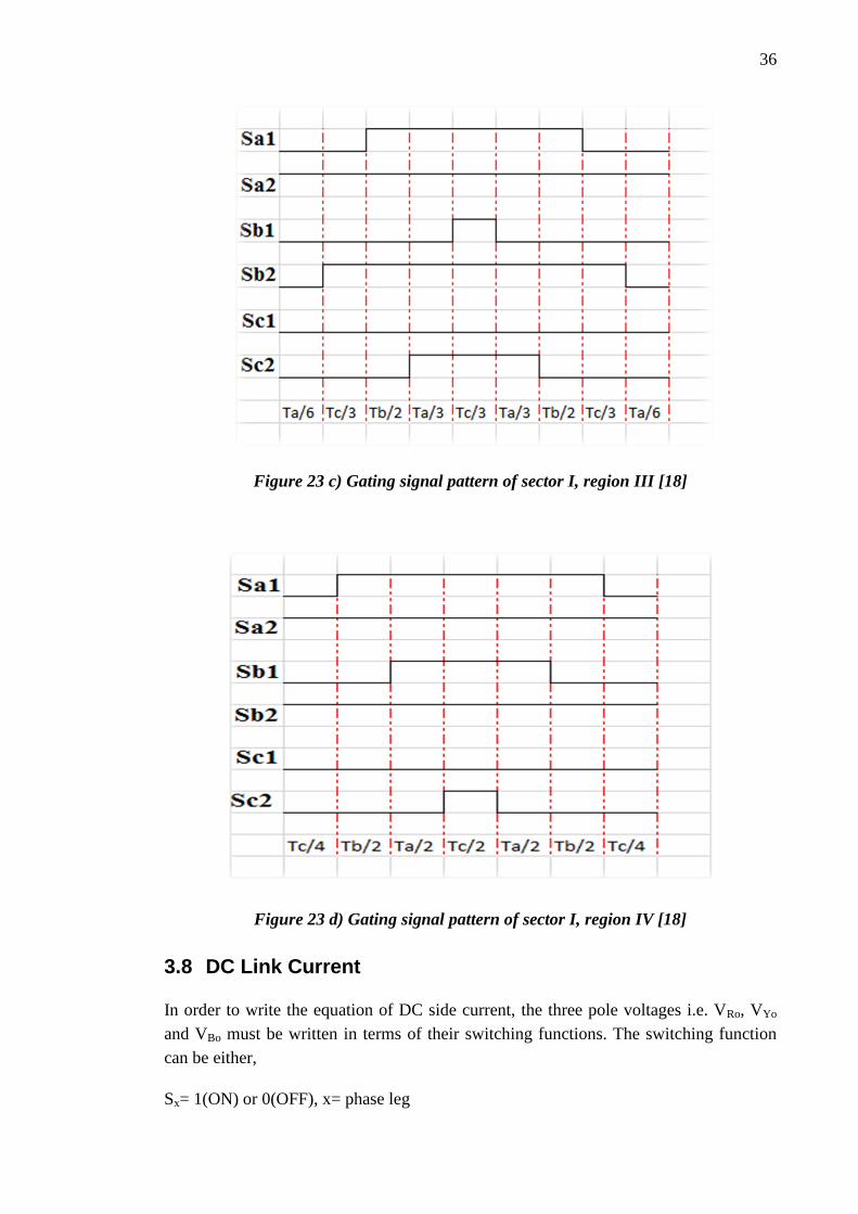
Table 6 Switching pattern of sector I
From table 6, it is concluded that only one phase is switched during each transition. For
e.g. in region II the transition from sequence 1 to sequence 2, R-φ is switched from 0 →
+ while the Y-φ and B-φ remains on their previous value i.e. „-„.
Region Switching Vectors
13-segments switching pattern
1 2 3 4 5 6 7 8 9 10 11 12 13
I V2 V4 V8 V1 V3 V7 V27 V7 V3 V1 V8 V4 V2
--- 0-- 00- 000 +00 ++0 +++ ++0 +00 000 00- 0-- ---
7-segment switching pattern
II 1 2 3 4 5 6 7
V4 V5 V6 V3 V6 V5 V4
0-- +-- +0- +00 +0- +-- 0--
9-segment switching pattern
III 1 2 3 4 5 6 7 8 9
V4 V8 V6 V3 V7 V3 V6 V8 V4
0-- 00- +0- +00 ++0 +00 +0- 00- 0--
7-segments switching pattern
IV 1 2 3 4 5 6 7
V8 V6 V9 V7 V6 V9 V8
00- +0- ++- ++0 ++- +0- 00-

30
Figure 19 13-segment switching pattern for sector I, region I
Figure 20 7-segment switching pattern for sector I, region II

31
Figure 21 9-segment switching pattern for sector I, region III
Figure 22 7-segments switching for sector I, region IV
Switching schemes for the remaining sectors are given in Appendix-IX.
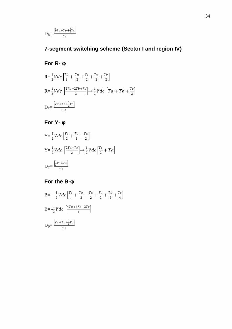
3.7 Duty Cycle Calculation
In this section the duty cycle of 3-phases will be calculated for all 4 region of sector I
which means for how much time all these 3-phases will remain ON from the entire Ts
second. From the above figures there are only three different DC levels available i.e. 1
2𝑉𝑑𝑐, 0Vdc, -
1
2𝑉𝑑𝑐, the ratio of the sum of the product of these levels with their
corresponding time duration to the total sampling time (Ts) gives the duty ratio.

32
13-segment switching scheme (Sector I and Region I):
For the R-φ
R= 1
2𝑉𝑑𝑐
𝑇𝑎
4+
𝑇𝑐
4+
𝑇𝑏
4+
𝑇𝑐
4+
𝑇𝑎
4 −
1
2𝑉𝑑𝑐
𝑇𝑏
8+
𝑇𝑏
8
R= 1
2𝑉𝑑𝑐
2𝑇𝑎+2𝑇𝑐+2𝑇𝑏+2𝑇𝑐+2𝑇𝑎−𝑇𝑏−𝑇𝑏
8 →
1
2𝑉𝑑𝑐
1
2𝑇𝑎 +
1
2𝑇𝑐
DR=
1
2𝑇𝑎+
1
2𝑇𝑐
𝑇𝑠
For the Y-φ
Y= 1
2𝑉𝑑𝑐
𝑇𝑐
4+
𝑇𝑏
4+
𝑇𝑐
4 −
1
2𝑉𝑑𝑐
𝑇𝑏
8+
𝑇𝑎
4+
𝑇𝑎
4+
𝑇𝑏
8
Y=1
2𝑉𝑑𝑐
2𝑇𝑐+2𝑇𝑏+2𝑇𝑐−𝑇𝑏−2𝑇𝑎−2𝑇𝑎−𝑇𝑏
8
DY= −
1
2𝑇𝑎+
1
2𝑇𝑐
𝑇𝑠
For the B-φ
B= 1
2𝑉𝑑𝑐
𝑇𝑏
4 −
1
2𝑉𝑑𝑐
𝑇𝑏
8+
𝑇𝑎
4+
𝑇𝑐
4+
𝑇𝑐
4+
𝑇𝑎
4+
𝑇𝑏
8
B=1
2𝑉𝑑𝑐
2𝑇𝑏−𝑇𝑏−2𝑇𝑎−2𝑇𝑐−2𝑇𝑐−2𝑇𝑎−𝑇𝑏
8
DB= −
1
2𝑇𝑎−
1
2𝑇𝑐
𝑇𝑠
7-segment switching scheme (Sector I and region II):
For R- φ
R= 1
2𝑉𝑑𝑐
𝑇𝑐
2+
𝑇𝑏
2+
𝑇𝑎
2+
𝑇𝑏
2+
𝑇𝑐
2
R= 1
2𝑉𝑑𝑐
𝑇𝑎+2𝑇𝑏+2𝑇𝑐
2 →
1
2𝑉𝑑𝑐
1
2𝑇𝑎 + 𝑇𝑏 + 𝑇𝑐
DR=
1
2𝑇𝑎+𝑇𝑏+𝑇𝑐
𝑇𝑠
For Y- φ

33
Y= -1
2𝑉𝑑𝑐
𝑇𝑎
4+
𝑇𝑐
2+
𝑇𝑐
2+
𝑇𝑎
4
Y= -1
2𝑉𝑑𝑐
𝑇𝑎+2𝑇𝑐+2𝑇𝑐+𝑇𝑎
4 →
1
2𝑉𝑑𝑐
𝑇𝑎
2+ 𝑇𝑐
DY=
1
2𝑇𝑎+𝑇𝑐
𝑇𝑠
For the B-φ
B= −1
2𝑉𝑑𝑐
𝑇𝑎
4+
𝑇𝑐
2+
𝑇𝑏
2+
𝑇𝑏
2+
𝑇𝑐
2+
𝑇𝑎
4
B=-1
2𝑉𝑑𝑐
𝑇𝑎+2𝑇𝑐+2𝑇𝑏+2𝑇𝑏+2𝑇𝑐+𝑇𝑎
4 →-
1
2𝑉𝑑𝑐
2𝑇𝑎+4𝑇𝑏+4𝑇𝑐
4
DB=
1
2𝑇𝑎+𝑇𝑏+𝑇𝑐
𝑇𝑠
9-segment switching scheme (Sector I and region III)
For R- φ
R= 1
2𝑉𝑑𝑐
𝑇𝑏
2+
𝑇𝑎
3+
𝑇𝑐
3+
𝑇𝑎
3+
𝑇𝑏
2
R= 1
2𝑉𝑑𝑐
3𝑇𝑏+2𝑇𝑎+2𝑇𝑐+2𝑇𝑎+3𝑇𝑏
6 →
1
2𝑉𝑑𝑐
2
3𝑇𝑎 + 𝑇𝑏 +
1
3𝑇𝑐
DR=
2
3𝑇𝑎+𝑇𝑏+
1
3𝑇𝑐
𝑇𝑠
For the Y-φ
Y= 1
2𝑉𝑑𝑐
𝑇𝑐
3 −
1
2𝑉𝑑𝑐
𝑇𝑎
6+
𝑇𝑎
6
Y=1
2𝑉𝑑𝑐
2𝑇𝑐−𝑇𝑎−𝑇𝑎
6
DY= −
1
3𝑇𝑎+
1
3𝑇𝑐
𝑇𝑠
For the B-φ
B= −1
2𝑉𝑑𝑐
𝑇𝑎
6+
𝑇𝑐
3+
𝑇𝑏
2+
𝑇𝑏
2+
𝑇𝑐
3+
𝑇𝑎
6
B= -1
2𝑉𝑑𝑐
2𝑇𝑎+4𝑇𝑐+6𝑇𝑏
6
34
DB=
1
3𝑇𝑎+𝑇𝑏+
2
3𝑇𝑐
𝑇𝑠
7-segment switching scheme (Sector I and region IV)
For R- φ
R= 1
2𝑉𝑑𝑐
𝑇𝑏
2+
𝑇𝑎
2+
𝑇𝑐
2+
𝑇𝑎
2+
𝑇𝑏
2
R= 1
2𝑉𝑑𝑐
2𝑇𝑎+2𝑇𝑏+𝑇𝑐
2 →
1
2𝑉𝑑𝑐 𝑇𝑎 + 𝑇𝑏 +
𝑇𝑐
2
DR= 𝑇𝑎+𝑇𝑏+
1
2𝑇𝑐
𝑇𝑠
For Y- φ
Y= 1
2𝑉𝑑𝑐
𝑇𝑎
2+
𝑇𝑐
2+
𝑇𝑎
2
Y= 1
2𝑉𝑑𝑐
2𝑇𝑎+𝑇𝑐
2 →
1
2𝑉𝑑𝑐
𝑇𝑐
2+ 𝑇𝑎
DY=
1
2𝑇𝑐+𝑇𝑎
𝑇𝑠
For the B-φ
B= −1
2𝑉𝑑𝑐
𝑇𝑐
4+
𝑇𝑏
2+
𝑇𝑎
2+
𝑇𝑎
2+
𝑇𝑏
2+
𝑇𝑐
4
B= -1
2𝑉𝑑𝑐
4𝑇𝑎+4𝑇𝑏+2𝑇𝑐
4
DB= 𝑇𝑎+𝑇𝑏+
1
2𝑇𝑐
𝑇𝑠

35
Figure 23 a) Gating signal pattern of sector I, region I [18]
Figure 23 b) Gating signal pattern of sector I, region II [18]
36
Figure 23 c) Gating signal pattern of sector I, region III [18]
Figure 23 d) Gating signal pattern of sector I, region IV [18]
3.8 DC Link Current
In order to write the equation of DC side current, the three pole voltages i.e. VRo, VYo
and VBo must be written in terms of their switching functions. The switching function
can be either,
Sx= 1(ON) or 0(OFF), x= phase leg

37
DC Icap
IdcIin
iR iY iB
3-LevelNPC
Figure 24 DC link current and each phase leg current
0.5RO R DCV S V 0.5YO Y DCV S V 0.5BO B DCV S V
For 3-φ star connected balanced load,
3
RY BRRN
V VV
3
YB RYYN
V VV
3
BR YBBN
V VV
For RL load,
RRN R
diV Ri L
dt → RN RR
V Ridi
dt L
After integrating on both sides gives the R-phase current,
2
0
RN RR
V Rii
L
Similarly for Y-φ,
YYN Y
diV Ri L
dt → YN YY
V Ridi
dt L
After integrating on both sides gives the Y-phase current,
2
0
YN YY
V Rii
L

38
For B-φ,
BBN B
diV Ri L
dt → BN BB
V Ridi
dt L
After integrating on both sides gives the B-phase current,
2
0
BN BB
V Rii
L
In general the DC link current is represented as,
DC R R Y Y B Bi S i S i S i
3.8.1 Average DC Link Current over a Sub-cycle:
0 1 2 7
iR,1
iY,1
iB,1
0
Idc iR
-iB
+-- ++---- +++
Figure 25 DC link current over a sub-cycle
0 0
1 1s sT T
DC R R Y Y B B
s s
i t S i S i S i tT T
The left hand side of the above equation represents the average DC link current.

39
, ,1 ,1 ,1 ,1 ,1 ,1
0 0 0
1 1 1s s sT T T
DC avg R R Y Y B B
s s s
i i S i S i ST T T
Where iR,1= Fundamental component of R-phase current
IY,1= Fundamental component of Y-phase current
IB,1= Fundamental component of B-phase current
The terms except iR,1, iY,1, iB,1 on the right hand side of the above equation forms a duty
ratio of each phase leg.
, ,1 ,1 ,1DC avg R R Y Y B Bi D i D i D i
The duty ratio of R-φ, Y-φ and B-φ can be written as,
,ON R
R
s
TD
T
,ON Y
Y
s
TD
T
,ON B
B
s
TD
T
The input DC current (Iin) is the average of DC link current (IDC) over a cycle.
2
,
0
1
2in DC avgI i t
3.9 Conclusion
In this chapter the theory, concept and background of three-level SVPWM has been
discussed in detail. In support of this statement power stage of NPC has been
developed. To develop space vector diagram mathematical calculation has been done
along with the different switching schemes to reduce total harmonic distortion. The
derivation of pole voltages with supporting waveform has been done based on the
selection of particular sector and region. Vector switching times is also calculated along
with the duty ratio of power switches.

40
3.10 FLOW CHART OF THE ALGORITHM
Figure 26 SVPWM algorithm representations in flow chart
Start
Calculate α and β at different
switching state
Calculate magnitude and
direction of ref. vector
Identify sector and region
Identify three nearest vectors
Dwell time calculation of these
vectors
Identify and apply switching
pattern
End
41
4. SIMULATIONS & RESULTS
4.1 Introduction
A simulation is a tool through which any physical process can be implemented to get
the behavior of that system. From the results obtained from simulations are very much
same as in physical environment. As far as this thesis is concerned, the simulation tool
box used for the implementation of three-level SVPWM algorithm is
MATLAB/Simulink. MATLAB environment provides the built-in library features. The
Simulink model contains different blocks to implement this algorithm included some
sub blocks and MATLAB Function blocks where the C-language code is generated. The
power circuit for three level SVPWM is generated with 12-IGBT‟s and producing an
inverter output with fundamental frequency of 50 Hz by incorporated 3-φ star
connected balance load.
The “Subsystem block” employs the Clark‟s transformation to convert three phase
quantities to stationary reference frame which is based on eq. 2.15 and 2.16. The
“Subsystem1 block” is the representation of sector selection which is fed from the
results obtained from Clark‟s transformation. The “Matlab Function1 block” employs
the criteria for region selection based on the values of X1, X2 and Xn discuss in section
3.4.5. The “Matlab Function block” performs a very important task, the dwell time (Ta,
Tb and Tc) calculation and vector switching states are performed simultaneously. This
block cannot run until or unless the earlier three blocks produce its output. In other
words, the outputs of these three blocks are cascaded to “Matlab Function block”. The
gating signals are generated as an output from this block which further drives the power
stage of NPC inverter. The scopes are connected in such a way that the line to neutral
and line to line voltage waveform are drawn.
4.2 Output from Clark’s transformation
The magnitude and angle of reference vector is shown in fig.27 and 28. The sub-blocks
of the main block is present in Appendix-I.

42
Figure 27 Magnitude of reference vector
Figure 28 Angular position of reference vector
4.3 Sector Selector
The sector selection block is driven with an angle. Some mathematical function and
logical functions have been incorporated to identify the sector. From the fig.29 the
reference vector passes through each sector with a fix step.

43
Figure 29 Output of sector determination block
The brief description of “Sector selection” block is given in Appendix-II
4.4 Region Selector
The entire space vector diagram is divided into 6-sectors, each sector has a same
methodolgy for switching stationary vectors. After each 60o degrees the new sector
arrived and same strategy is applied over it which makes the system more complex. The
alternate way is to bring back each sector to sector I or in other words each sector is
multiple of 60o. The resulting angle is obtained by subtracting the calculated angle from
multiple of 60 as given below,
Alpha=angle–(sector-1)60 (27)
The contents of region selection is given in Appendix-III.
Figure 30 Output of region selection block

44
The “dwell time calculations” block performs the calculation for the dwell time of each
region of sector I (Tax, Tbx, Tcx) where x= region number. The input necessary to drive
this block requires sector number, region number, modulation index, magnitude and
angle of reference vector. The outputs are 12 dwell time signals. The sub-block is the
implementation of equations given in table 4. Based on these values the stationary
vectors are applied for that much of duration. The contents of this block are presented in
Appendix-IV.
4.5 Gating Signal Generator
The output of this block also generates the gating signals to drive the power switches in
NPC. The bottom two switches of each phase leg are connected in complementary
fashion so for these switches gating signals are generated by inverted the status of upper
two switches.
Figure 31 Gating signal for R-phase leg (i) SA1 (ii) SA1' (iii) SA2 (iv) SA2'
After the implementation of theory described in the above section gives the pole voltage
which is measured from the middle of each phase leg to the DC neutral point „o‟. The
NPC inverter is operated with 440V DC input which produces an output having a three
level i.e. 220V, 0V and -220V.
The SimPowerSystem is a modern design tool used to employ the NPC inverter. It uses
Simulink in order to implement its features. Not only can draw electrical circuit and
power network rapidly [7] but analyze the data in an efficient manner.
4.6 Model Parameters
These simulation runs with the following parameters,
Vdc= 440V, m= 0.95, fs= 2 kHz, Rload= 10Ω, Lload= 15mH and f1= 50Hz.
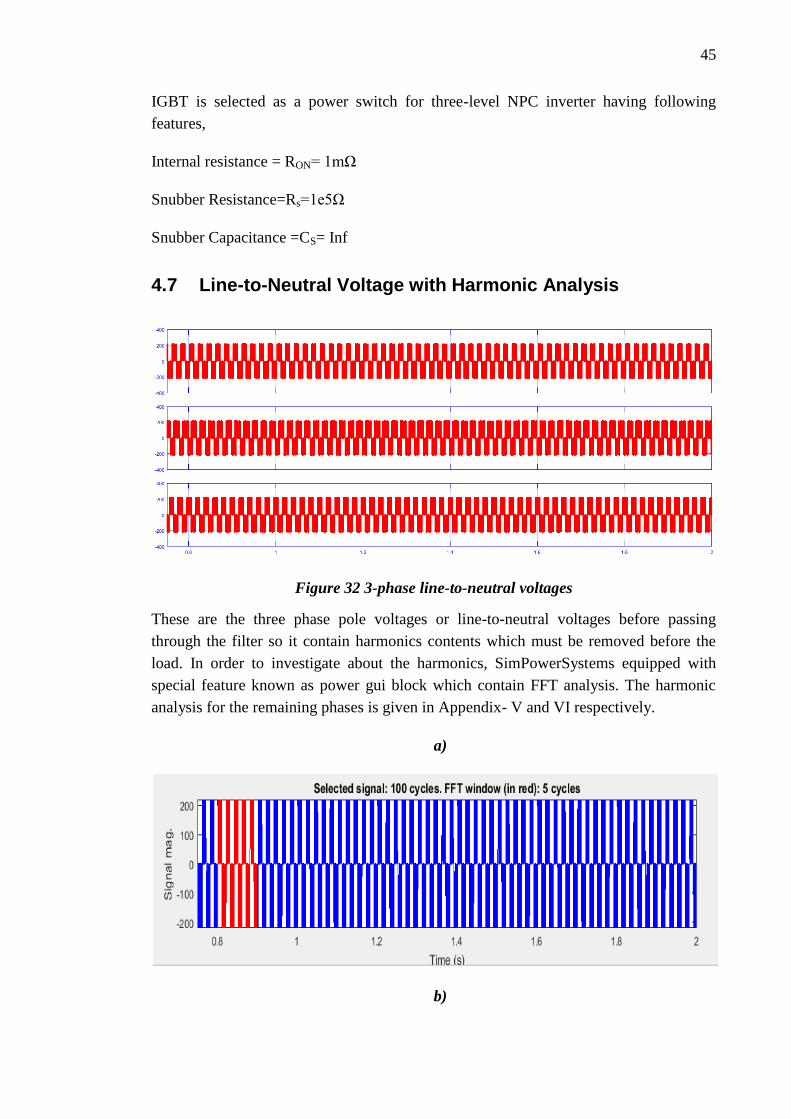
45
IGBT is selected as a power switch for three-level NPC inverter having following
features,
Internal resistance = RON= 1mΩ
Snubber Resistance=Rs=1e5Ω
Snubber Capacitance =CS= Inf
4.7 Line-to-Neutral Voltage with Harmonic Analysis
Figure 32 3-phase line-to-neutral voltages
These are the three phase pole voltages or line-to-neutral voltages before passing
through the filter so it contain harmonics contents which must be removed before the
load. In order to investigate about the harmonics, SimPowerSystems equipped with
special feature known as power gui block which contain FFT analysis. The harmonic
analysis for the remaining phases is given in Appendix- V and VI respectively.
a)
b)
46
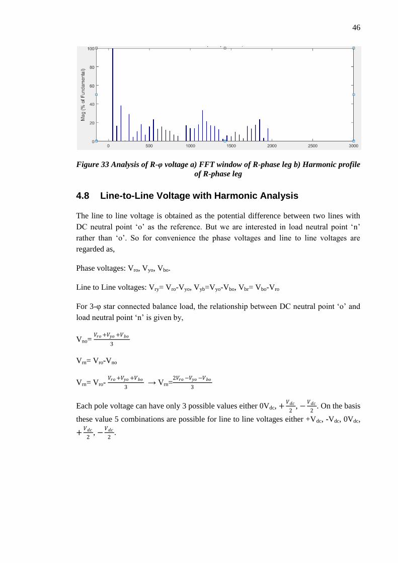
Figure 33 Analysis of R-φ voltage a) FFT window of R-phase leg b) Harmonic profile
of R-phase leg
4.8 Line-to-Line Voltage with Harmonic Analysis
The line to line voltage is obtained as the potential difference between two lines with
DC neutral point „o‟ as the reference. But we are interested in load neutral point „n‟
rather than „o‟. So for convenience the phase voltages and line to line voltages are
regarded as,
Phase voltages: Vro, Vyo, Vbo.
Line to Line voltages: Vry= Vro-Vyo, Vyb=Vyo-Vbo, Vbr= Vbo-Vro
For 3-φ star connected balance load, the relationship between DC neutral point „o‟ and
load neutral point „n‟ is given by,
Vno= 𝑉𝑟𝑜 +𝑉𝑦𝑜 +𝑉𝑏𝑜
3
Vrn= Vro-Vno
Vrn= Vro- 𝑉𝑟𝑜 +𝑉𝑦𝑜 +𝑉𝑏𝑜
3 → Vrn=
2𝑉𝑟𝑜 −𝑉𝑦𝑜 −𝑉𝑏𝑜
3
Each pole voltage can have only 3 possible values either 0Vdc, +𝑉𝑑𝑐
2, −
𝑉𝑑𝑐
2. On the basis
these value 5 combinations are possible for line to line voltages either +Vdc, -Vdc, 0Vdc,
+𝑉𝑑𝑐
2, −
𝑉𝑑𝑐
2.

47
Figure 34 Line-to-Line voltages between R-phase and Y-phase
a)
b)
Figure 35 Analysis of line- to-line voltage a) FFT window of line-to-line voltage
b) Harmonic profile of line-to-line voltage
4.9 Implementation of Filter
The output produce by an inverter contain some harmonic contents which need to be
removed before applying it to the load. Only the fundamental component is allowed to
pass to the load. These harmonic can be separated from its harmonic contents by
designing a filter having a resonant frequency of 50Hz.
𝑓𝑟 = 1
2𝜋 𝐿𝐶 → LC= 1.012949*10−5
By deduce the above value gives, L=6.330mH and C=1600μF.

48
a)
b)
Figure 36 Analysis of R- φ current a) R-phase current waveform b) Harmonic profile
of R-φ current
From the above figure it is easily deduced that only the fundamental components appear
while the harmonic contents are completely removed.
The contents of Y-φ and B-φ are given in Appendix-VII and VIII.

49
5. CONCLUSION
This thesis has given a broad review about the concept, theory and basic principle of
multilevel inverter. After careful consideration between different modulation
techniques, it is concluded that the space-vector-pulse-width modulation (SVPWM) is
found to be most popular technique. The brief introduction of carrier based modulation
technique is also discussed to get better understanding. While comparing the carrier
based pulse width modulation and space-vector-pulse-width modulation, SVPWM
carries better DC bus utilization causing a better production of fundamental component
by means of amplitude. By implementing this technique the amount of total harmonic
distortion (THD) is also get reduced. After careful consideration between the two-level
and multilevel inverter, multilevel converter carries better utilization of fundamental
component and better profile of THD. However, large number of components will
utilize. The name multilevel arise from the fact that how many voltage level the output
contains? As far as this thesis is concerned, the pole voltage contains three different
voltage levels so it is regarded as three-level SVPWM voltage source inverter. The
more the number of levels the better the output is. It closely resembles to sinusoidal
output. The three-level inverter is also regarded as neutral point clamp inverter which is
commonly used for the purpose of variable frequency drive (VFD) applications. This
thesis is also supported with complex mathematical calculation and in order to get better
understanding of the theory some waveforms have also been drawn.
To prove this theory, some simulations are also been taken into account in
MATLAB/SIMULINK. The overview of each block used in this environment is also
presented. The results obtained by utilizing practical values of R-L load. The harmonic
contents at each output stage are analyzed by utilizing the FFT analysis tool which is
incorporated in SimPowerSys tool box.
5.1 Future Work Proposal
Implementation of this algorithm in over-modulation region.
Designing of PI controller for dynamic voltage balancing between the
capacitors.
Investigate 3-Level algorithm as an equivalent 2-Level parallel inverter for
reducing mathematical calculation.
Further implementing THD reduction methods.
Implementation of Selective Harmonic Elimination (SHE) technique to reduce
higher order harmonics.

50
REFERENCES
[1] Mitosz Miskiewicz, Arnstein Johannesen, “A Three-Level Space Vector
Modulation Strategy for Two-Level Parallel Inverters”, M.S thesis, Inst. of
Energy Tech., Aalborg Univ., Denmark, 2009.
[2] Bimal K. Bose, (2002), Modern Power Electronics and AC Drives, Prentice Hall,
New Jersey
[3] Weixing Feng, “Space Vector Modulation for Three-Level Neutral Point Clamped
Inverter”, M.Sc Thesis, ECE, Ryerson Univ., Toronto, Canada, 2004.
[4] P. Tripura, Y.S.Kishore Babu, Y.R.Tagore, “ Space Vector Pulse Width
Modulation Schemes for Two-Level Voltage Source Inverter”, Vignan‟s Nirula
Inst. of Tech. & Science, EEE Dept., India, Vignan Univ. Vadlamudi, School of
Elect. Eng., India, ACEEE Int. J. on Control System and Instrumentation, Vol. 02,
No.3, Oct. 2011.
[5] Dr. Yashvant Jani, Graeme Clark, Renesas Electronics, “MCU with FPU allows
advanced Motor Control Solutions”, http://www.powersystemsdesign.com/mcu-
with-fpu-allows-advanced-motor-control-solutions, 24 April, 2012.
[6] ABD Almula G. M. Gebreel, “Simulation and Implementation of Two Level and
Three-Level Inverters by MATLAB and RT-LAB”, M.S thesis, ECS, Ohio State
Univ., 2011.
[7] SimPowerSystems For Use with Simulink, User‟s Guide, Version 3, Sept. 2003
[8] Suresh L., Mahesh K., Janardhna M. and Mahesh M., “Simulation of Space
Vector Pulse Width Modulation for Voltage Source Inverter Using
MATLAB/Simulink”, J. Automation & Systems Engineering, 133-140, March
2014.
[9] S. Manivannan, S. Veerakumar, P. Karuppusamy, A. Nandhakumar,
“Performance Analysis of Three Phase Voltage Source Inverter Fed Induction
Motor Drive with Possible Switching Sequence Execution in SVPWM”,
IJAREEIE, Vol.3, Issue 6, June 2014.
[10] Bimal K. Bose, Modern Power Electronics and AC Drives. New Jersey: Prentice
Hall, 2002.
[11] Vieri Xue, “Center-Aligned SVPWM Realization for 3- Phase 3- Level Inverter”,
Application Report, Texas Inst., Oct. 2012
[12] Atif Iqbal, Adoum Lamine, Imtiaz Ashraf, Mohibullah, “MATLAB/SIMULINK
MODEL OF SPACE VECTOR PWM FOR THREE-PHASE VOLTAGE

51
SOURCE INVERTER”, Aligarh Muslim Univ. India, Liverpool John Moores
Univ. U.K.
[13] D.W. Kang, C.S. Ma, T.J. Kim and D.S. Hyun, “Simple control strategy for
balancing the DC-link voltage of neutral-point-clamped inverter at low
modulation index”, IEE Proc.-Electr. Power Appl., Vol. 151, No. 5, September
2004.
[14] T. Abdelkrim, E.M. Berkouk, Aeh. Benkhelifa, K. Benamrane, T. Benslimane,
“Neutral Point Potential Balancing Algorithm for Autonomous Three-Level Shunt
Active Power Filter”, ARU on Renewable Energies, Ghardaïa, Algeria, Lab. of
Process Control, PNS, Algiers, Algeria, LAEIE Uni. of BoumerdesUni of M‟sila,
Algeria.
[15] K Abhishekam, K Sri Gowri, “Simplified Space Vector PWM Algorithm for a
Three Level Inverter”, Innovative Systems Design and Eng., ISSN 2222-1727,
Vol. 6, No.2, 2015.
[16] Ayse Kocalmis, Sedat Sunter, “Simulation of a Space Vector PWM Controller for
a Three –Level Voltage –Fed Inverter Motor Drive,” pp.1915-1920.
[17] Mahmoud Kassas, Naseer Ahmed, “Simulation and Implementation of Space
Vector PWM Using Look-Up Table”, Arab J Sci. Eng.(2014) 39:4815-4828.
[18] Dong-Myung Lee, Jin-Woo Jung, Sang-Shin Kwak, “Simple Space Vector PWM
Scheme for 3-Level NPC Inverters Including the Overmodulation Region”,
Journal of Power Electronics, Vol.11, No.5, Sept. 2011.
[19] Nashiren F. Mailah, Senan M. Bashi, Ishak Aris, Norman Mariun, “Neutral-Point-
Clamped Multilevel Inverter Using Space Vector Modulation”, European Journal
of Scientific research, ISSN 1450-216X, Vol.28 No.1, pp.82-91, 2009.
[20] B.Urmila, D. Subba Rayudu, “Optimum Space Vector PWM Algorithm for
Three-Level Inverter”, ARPN Journal of Eng. And Applied Sciences, VOL.6,
No.9, Sept. 2011.
[21] Sveinung Floten, Tor Stian Haug, “Modulation Methods for Neutral-Point-
clamped Three-Level Inverter”, M.Sc Thesis, Elec. Power Eng., NTNU, June
2010.
[22] K.Gopala Krishna, T. Kranthi Kumar, and P. Venugopal Rao “Better DC Bus
Utilization and Torque Ripple Reduction by using SVPWM for VSI fed Induction
Motor Drive”, International Journal of Computer and Electrical Engineering,
Vol.4, No.2, April 2012.

6. APPENDICES
Appendix I: Implementation of the conversion of three phase quantities to stationary
reference frame

Appendix II: Mathematical model of “Sector Selection” block

Appendix III: Mathematical model of “Region selection” block

Appendix IV: Mathematical model of “Dwell time calculation” block

a)
b)
Appendix V: Analysis of Y-φ a) FFT window of Y-phase b) Harmonic analysis of Y-
phase

a)
b)
Appendix VI: Analysis of B-φ a) FFT window of B-phase b) Harmonic analysis of B-
phase

a)
b)
Appendix VII: Analysis of Y-Phase current a) current waveform b) Harmonic
analysis

a)
b )
Appendix VIII: Analysis of B-Phase current a) current waveform b) Harmonic
analysis

13-Segment Scheme
S2,R1
𝑉27 𝑉7 𝑉12 𝑉1 𝑉8 𝑉13 𝑉2 𝑉13 𝑉8 𝑉1 𝑉12 𝑉7 𝑉27
+++ +++ 0+0 000 00- -0- --- -0- 00- 000 0+0 ++0 +++
𝑇𝑏
8
𝑇𝑐4
𝑇𝑏
4
𝑇𝑏
4
𝑇𝑐4
𝑇𝑎4
𝑇𝑏
4
𝑇𝑎4
𝑇𝑐4
𝑇𝑏
4
𝑇𝑎4
𝑇𝑐4
𝑇𝑏
8
S3,R1
𝑉2 𝑉13 𝑉15 𝑉1 𝑉12 𝑉14 𝑉27 𝑉14 𝑉12 𝑉1 𝑉15 𝑉13 𝑉2
--- -0- -00 000 0+0 0++ +++ 0++ 0+0 000 -00 -0- ---
𝑇𝑏
8
𝑇𝑎4
𝑇𝑐4
𝑇𝑏
4
𝑇𝑎4
𝑇𝑐4
𝑇𝑏
4
𝑇𝑐4
𝑇𝑎4
𝑇𝑏
4
𝑇𝑐4
𝑇𝑎4
𝑇𝑏
8
S4,R1
𝑉27 𝑉14 𝑉19 𝑉1 𝑉15 𝑉20 𝑉2 𝑉20 𝑉15 𝑉1 𝑉19 𝑉14 𝑉27
+++ 0++ 00+ 000 -00 --0 --- --0 -00 000 00+ 0++ +++
𝑇𝑏
8
𝑇𝑐4
𝑇𝑎4
𝑇𝑏
4
𝑇𝑐4
𝑇𝑎4
𝑇𝑏
4
𝑇𝑎4
𝑇𝑐4
𝑇𝑏
4
𝑇𝑎4
𝑇𝑐4
𝑇𝑏
8
S5,R1
𝑉2 𝑉20 𝑉24 𝑉1 𝑉19 𝑉23 𝑉27 𝑉23 𝑉19 𝑉1 𝑉24 𝑉20 𝑉2
--- --0 0-0 000 00+ +0+ +++ +0+ 00+ 000 0-0 --0 ---
𝑇𝑏
8
𝑇𝑎4
𝑇𝑐4
𝑇𝑏
4
𝑇𝑎4
𝑇𝑐4
𝑇𝑏
4
𝑇𝑐4
𝑇𝑎4
𝑇𝑏
4
𝑇𝑐4
𝑇𝑎4
𝑇𝑏
8
S6,R1
𝑉27 𝑉23 𝑉3 𝑉1 𝑉24 𝑉4 𝑉2 𝑉4 𝑉24 𝑉1 𝑉3 𝑉23 𝑉27
+++ +0+ +00 000 0-0 0-- --- 0-- 0-0 000 +00 +0+ +++
𝑇𝑏
8
𝑇𝑐4
𝑇𝑎4
𝑇𝑏
4
𝑇𝑐4
𝑇𝑎4
𝑇𝑏
4
𝑇𝑎4
𝑇𝑐4
𝑇𝑏
4
𝑇𝑎4
𝑇𝑐4
𝑇𝑏
8

7-Segment Scheme
S2,R2
𝑉7 𝑉9 𝑉10 𝑉8 𝑉10 𝑉9 𝑉7
++0 ++- 0+- 00- 0+- ++- ++0
𝑇𝑐4
𝑇𝑎2
𝑇𝑏
2
𝑇𝑐2
𝑇𝑏
2
𝑇𝑎2
𝑇𝑐4
S3,R2
𝑉13 𝑉11 𝑉16 𝑉12 𝑉16 𝑉11 𝑉13
-0- -+- -+0 0+0 -+0 -+- -0-
𝑇𝑎4
𝑇𝑐2
𝑇𝑏
2
𝑇𝑎2
𝑇𝑏
2
𝑇𝑐2
𝑇𝑎4
S4,R2
𝑉14 𝑉17 𝑉18 𝑉15 𝑉18 𝑉17 𝑉14
0++ -++ -0+ -00 -0+ -++ 0++
𝑇𝑐4
𝑇𝑎2
𝑇𝑏
2
𝑇𝑐2
𝑇𝑏
2
𝑇𝑎2
𝑇𝑐4
S5,R2
𝑉20 𝑉21 𝑉22 𝑉19 𝑉22 𝑉21 𝑉20
--0 --+ 0-+ 00+ 0-+ --+ --0
𝑇𝑎4
𝑇𝑐2
𝑇𝑏
2
𝑇𝑎2
𝑇𝑏
2
𝑇𝑐2
𝑇𝑎4
S6,R2
𝑉23 𝑉25 𝑉26 𝑉24 𝑉26 𝑉25 𝑉23
+0+ +-+ +-0 0-0 +-0 +-+ +0+
𝑇𝑐4
𝑇𝑎2
𝑇𝑏
2
𝑇𝑐2
𝑇𝑏
2
𝑇𝑎2
𝑇𝑐4

9-Segment Scheme
S2,R3
𝑉7 𝑉12 𝑉10 𝑉8 𝑉13 𝑉8 𝑉10 𝑉12 𝑉7
++0 0+0 0+- 00- -0- 00- 0+- 0+0 ++0
𝑇𝑐4
𝑇𝑎4
𝑇𝑏
2
𝑇𝑐4
𝑇𝑎2
𝑇𝑐4
𝑇𝑏
2
𝑇𝑎4
𝑇𝑐4
S3,R3
𝑉13 𝑉15 𝑉16 𝑉12 𝑉14 𝑉12 𝑉16 𝑉15 𝑉13
-0- -00 -+0 0+0 0++ 0+0 -+0 -00 -0-
𝑇𝑎4
𝑇𝑐4
𝑇𝑏
2
𝑇𝑎4
𝑇𝑐2
𝑇𝑎4
𝑇𝑏
2
𝑇𝑐4
𝑇𝑎4
S4,R3
𝑉14 𝑉19 𝑉18 𝑉15 𝑉20 𝑉15 𝑉18 𝑉19 𝑉14
0++ 00+ -0+ -00 --0 -00 -0+ 00+ 0++
𝑇𝑐4
𝑇𝑎4
𝑇𝑏
2
𝑇𝑐4
𝑇𝑎2
𝑇𝑐4
𝑇𝑏
2
𝑇𝑎4
𝑇𝑐4
S5,R3
𝑉20 𝑉24 𝑉22 𝑉19 𝑉23 𝑉19 𝑉22 𝑉24 𝑉20
--0 0-0 0-+ 00+ +0+ 00+ 0-+ 0-0 --0
𝑇𝑎4
𝑇𝑐4
𝑇𝑏
2
𝑇𝑎4
𝑇𝑐2
𝑇𝑎4
𝑇𝑏
2
𝑇𝑐4
𝑇𝑎4
S6,R3
𝑉23 𝑉3 𝑉26 𝑉24 𝑉4 𝑉24 𝑉26 𝑉3 𝑉23
+0+ ++0 +-0 0-0 0-- 0-0 +-0 +00 +0+
𝑇𝑐4
𝑇𝑎4
𝑇𝑏
2
𝑇𝑐4
𝑇𝑎2
𝑇𝑐4
𝑇𝑏
2
𝑇𝑎4
𝑇𝑐4
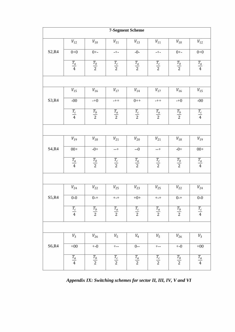
7-Segment Scheme
S2,R4
𝑉12 𝑉10 𝑉11 𝑉13 𝑉11 𝑉10 𝑉12
0+0 0+- -+- -0- -+- 0+- 0+0
𝑇𝑎4
𝑇𝑏
2
𝑇𝑐2
𝑇𝑎2
𝑇𝑐2
𝑇𝑏
2
𝑇𝑎4
S3,R4
𝑉15 𝑉16 𝑉17 𝑉14 𝑉17 𝑉16 𝑉15
-00 -+0 -++ 0++ -++ -+0 -00
𝑇𝑐4
𝑇𝑏
2
𝑇𝑎2
𝑇𝑐2
𝑇𝑎2
𝑇𝑏
2
𝑇𝑐4
S4,R4
𝑉19 𝑉18 𝑉21 𝑉20 𝑉21 𝑉18 𝑉19
00+ -0+ --+ --0 --+ -0+ 00+
𝑇𝑎4
𝑇𝑏
2
𝑇𝑐2
𝑇𝑎2
𝑇𝑐2
𝑇𝑏
2
𝑇𝑎4
S5,R4
𝑉24 𝑉22 𝑉25 𝑉23 𝑉25 𝑉22 𝑉24
0-0 0-+ +-+ +0+ +-+ 0-+ 0-0
𝑇𝑐4
𝑇𝑏
2
𝑇𝑎2
𝑇𝑐2
𝑇𝑎2
𝑇𝑏
2
𝑇𝑐4
S6,R4
𝑉3 𝑉26 𝑉5 𝑉4 𝑉5 𝑉26 𝑉3
+00 +-0 +-- 0-- +-- +-0 +00
𝑇𝑎4
𝑇𝑏
2
𝑇𝑐2
𝑇𝑎2
𝑇𝑐2
𝑇𝑏
2
𝑇𝑎4
Appendix IX: Switching schemes for sector II, III, IV, V and VI

a)
b)
Appendix IX: a) Simulink model of 3-level inverter b) power stage of the inverter


![MGT201 Subjective Material Mega File + Uzair Husnain[1]](https://img.pdfslide.us/doc/110x75/577d29da1a28ab4e1ea80e57/mgt201-subjective-material-mega-file-uzair-husnain1.jpg)


![Author: Balagamwala, Muhammad Uzair [FIN] Created Date: 8/26/2019 4:26:21 PM](https://img.pdfslide.us/doc/110x75/60e04729b13a6f70a2686d7e/-author-balagamwala-muhammad-uzair-fin-created-date-8262019-42621-pm.jpg)