Embed Size (px)
Citation preview
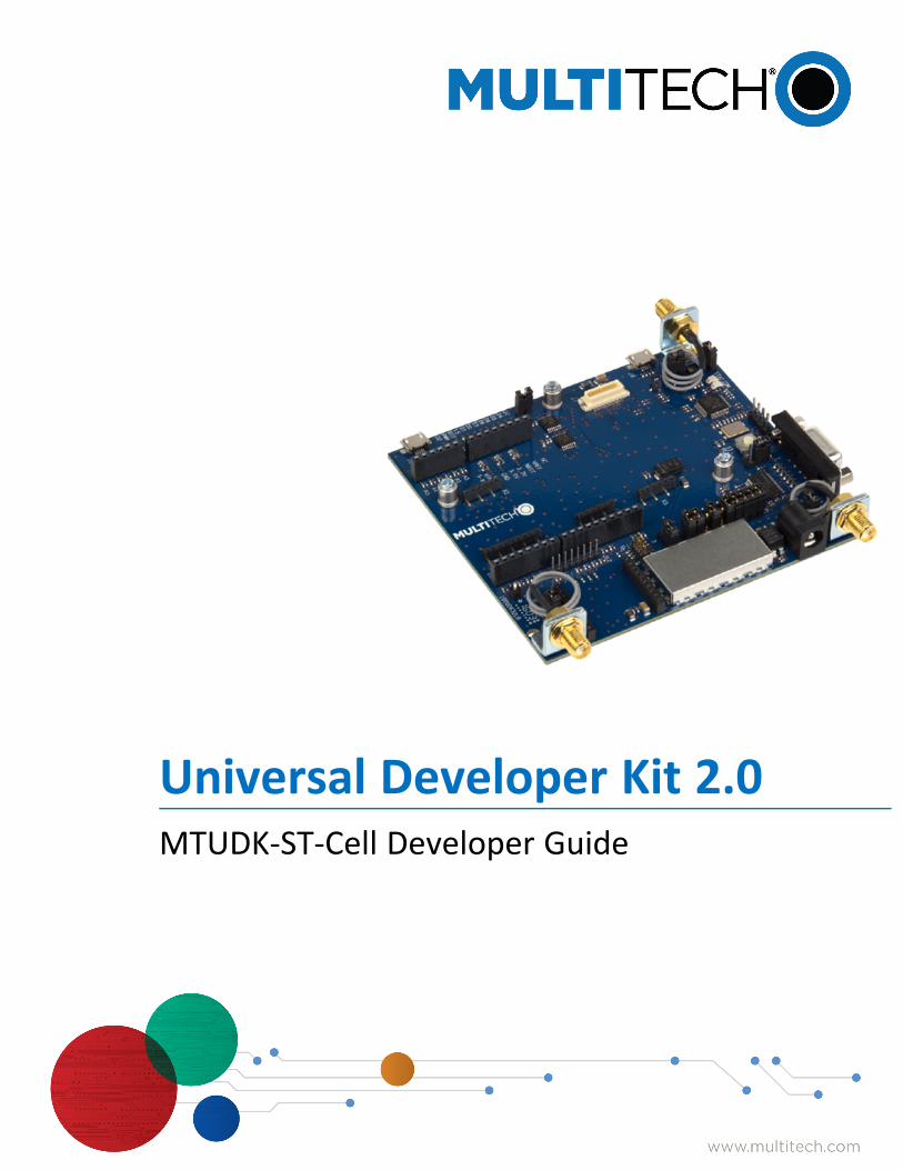
Universal Developer Kit 2.0MTUDK-ST-Cell Developer Guide

UNIVERSAL DEVELOPER KIT 2.0 DEVELOPER GUIDE
2 Universal Developer Kit 2.0 MTUDK-ST-Cell Developer Guide
Universal Developer Kit 2.0 Developer GuideModels: MTUDK-ST-Cell with DB9 RS-232 Connector
Part Number: S000693, Version 1.0
CopyrightThis publication may not be reproduced, in whole or in part, without the specific and express prior written permission signed by an executive officer ofMulti-Tech Systems, Inc. All rights reserved. Copyright © 2018 by Multi-Tech Systems, Inc.
Multi-Tech Systems, Inc. makes no representations or warranties, whether express, implied or by estoppels, with respect to the content, information,material and recommendations herein and specifically disclaims any implied warranties of merchantability, fitness for any particular purpose and non-infringement.
Multi-Tech Systems, Inc. reserves the right to revise this publication and to make changes from time to time in the content hereof without obligation ofMulti-Tech Systems, Inc. to notify any person or organization of such revisions or changes.
Trademarks and Registered TrademarksMultiTech, MultiConnect, SocketModem, and the MultiTech logo are registered trademarks of Multi-Tech Systems, Inc. All other brand and product namesare trademarks or registered trademarks of their respective companies.
Legal NoticesThe MultiTech products are not designed, manufactured or intended for use, and should not be used, or sold or re-sold for use, in connection withapplications requiring fail-safe performance or in applications where the failure of the products would reasonably be expected to result in personal injury ordeath, significant property damage, or serious physical or environmental damage. Examples of such use include life support machines or other lifepreserving medical devices or systems, air traffic control or aircraft navigation or communications systems, control equipment for nuclear facilities, ormissile, nuclear, biological or chemical weapons or other military applications (“Restricted Applications”). Use of the products in such RestrictedApplications is at the user’s sole risk and liability.
MULTITECH DOES NOT WARRANT THAT THE TRANSMISSION OF DATA BY A PRODUCT OVER A CELLULAR COMMUNICATIONS NETWORK WILL BEUNINTERRUPTED, TIMELY, SECURE OR ERROR FREE, NOR DOES MULTITECH WARRANT ANY CONNECTION OR ACCESSIBILITY TO ANY CELLULARCOMMUNICATIONS NETWORK. MULTITECH WILL HAVE NO LIABILITY FOR ANY LOSSES, DAMAGES, OBLIGATIONS, PENALTIES, DEFICIENCIES, LIABILITIES,COSTS OR EXPENSES (INCLUDING WITHOUT LIMITATION REASONABLE ATTORNEYS FEES) RELATED TO TEMPORARY INABILITY TO ACCESS A CELLULARCOMMUNICATIONS NETWORK USING THE PRODUCTS.
The MultiTech products and the final application of the MultiTech products should be thoroughly tested to ensure the functionality of the MultiTechproducts as used in the final application. The designer, manufacturer and reseller has the sole responsibility of ensuring that any end user product intowhich the MultiTech product is integrated operates as intended and meets its requirements or the requirements of its direct or indirect customers.MultiTech has no responsibility whatsoever for the integration, configuration, testing, validation, verification, installation, upgrade, support or maintenanceof such end user product, or for any liabilities, damages, costs or expenses associated therewith, except to the extent agreed upon in a signed writtendocument. To the extent MultiTech provides any comments or suggested changes related to the application of its products, such comments or suggestedchanges is performed only as a courtesy and without any representation or warranty whatsoever.
Contacting MultiTech
Knowledge BaseThe Knowledge Base provides immediate access to support information and resolutions for all MultiTech products. Visit http://www.multitech.com/kb.go.
Support PortalTo create an account and submit a support case directly to our technical support team, visit: https://support.multitech.com.
SupportBusiness Hours: M-F, 8am to 5pm CT
Country By Email By Phone
Europe, Middle East, Africa: [email protected] +(44) 118 959 7774
U.S., Canada, all others: [email protected] (800) 972-2439 or (763) 717-5863
WarrantyTo read the warranty statement for your product, visit www.multitech.com/warranty.go. For other warranty options, visit www.multitech.com/es.go.
World Headquarters
Multi-Tech Systems, Inc.
2205 Woodale Drive, Mounds View, MN 55112
Phone: (800) 328-9717 or (763) 785-3500
Fax (763) 785-9874
CONTENTS
Universal Developer Kit 2.0 MTUDK-ST-Cell Developer Guide 3
ContentsChapter 1 – Developer Kit Introduction.................................................................................................................... 4
Overview ....................................................................................................................................................................... 4Features ...................................................................................................................................................................... 4Device Specific Documentation .................................................................................................................................. 4
MTUDK2-ST-CELL Developer Kit Contents ................................................................................................................... 4
Chapter 2 – Board Components ............................................................................................................................... 6Developer Board .......................................................................................................................................................... 6Developer Board Connectors ........................................................................................................................................ 7
Board Components ..................................................................................................................................................... 7LED Indicators ............................................................................................................................................................. 8
Chapter 3 – Installation and Operation .................................................................................................................... 9Installing a SIM Card ..................................................................................................................................................... 9
Installing a SIM Card on a SocketModem .................................................................................................................. 9Installing a SIM Card on a DragonFly ......................................................................................................................... 9
Installing a SocketModem on the Developer Board ................................................................................................... 10Installing a Dragonfly on the Developer Board........................................................................................................... 11Arduino Shield............................................................................................................................................................. 11
Installing an Arduino Shield with a Dragonfly........................................................................................................... 11Dragonfly Arduino Pins ............................................................................................................................................. 12Installing an Arduino Shield with a SocketModem................................................................................................... 13
Attaching Power Supply Blades .................................................................................................................................. 14Power Supply and Blades.......................................................................................................................................... 14Attaching the Blades ................................................................................................................................................. 14
SMA to U.FL Cables ..................................................................................................................................................... 15Connecting an Antenna through the Developer Board Connectors........................................................................... 15
Chapter 4 – Block Diagram and Schematics............................................................................................................ 16Block Diagram ............................................................................................................................................................. 17Schematics .................................................................................................................................................................. 18
Chapter 5 – Design Considerations......................................................................................................................... 23Noise Suppression Design ........................................................................................................................................... 23PC Board Layout Guideline ......................................................................................................................................... 23Electromagnetic Interference .................................................................................................................................... 23Electrostatic Discharge Control................................................................................................................................... 24USB Design ................................................................................................................................................................. 24
DEVELOPER KIT INTRODUCTION
4 Universal Developer Kit 2.0 MTUDK-ST-Cell Developer Guide
Chapter 1 – Developer Kit IntroductionOverviewThe MTUDK2-ST-Cell Universal Developer Kit supports development with cellular SocketModem, Dragonfly, andmDot devices. Use the developer board to streamline your development efforts and evaluate your products andapplications. Easily plug in your communications device and use the developer kit for testing, programming andevaluation.
Note: Use this Developer Guide for developing with a SocketModem or Dragonfly. If developing with an mDot,use the MultiConnect® mDotTM Developer Guide, which includes device and developer board informationspecific to mDots. Go to the mDot Developer Kit page at http://www.multitech.com/models/94558010LF.Warning: Do not use an mDot and a Dragonfly or Socketmodem on this board at the same time. Doing to maydamage both devices.
Features5V-9V power inputSelectable 3.3V or 5V on board power supplyUSB and serial interfacesUSB port for mbed development environmentRS-232 DB-9 connector for serial interfaceArduino shield socket
Device Specific DocumentationRefer to the Device Guide for your SocketModem or Dragonfly model for specifications, pin information,mechanical drawings, labeling, regulatory information, and other model specific details.
MTUDK2-ST-CELL Developer Kit ContentsThe MTUDK2-ST-CELL Developer Kit includes the following:
Developer Board 1 - MTUDK 2.0 Cell Developer Board
Power Supply 1 - 100-240V 9V-1.7A power supply with removable blades
1 - NAM blade/plug,
1 - EURO blade/plug
1 - UK blade/plug
1 - AU/NZ blade/plug
Cables 1 - Micro USB Cable
3 - SMA-U.FL Antenna Cables (attached to developer board)
Antennas 1 - 3.3V magnetic GPS Antenna
2 - 700-2600 MHz Antennas
Customer Notices Quick Start
DEVELOPER KIT INTRODUCTION
Universal Developer Kit 2.0 MTUDK-ST-Cell Developer Guide 5
Additional One promotional screwdriver
BOARD COMPONENTS
6 Universal Developer Kit 2.0 MTUDK-ST-Cell Developer Guide
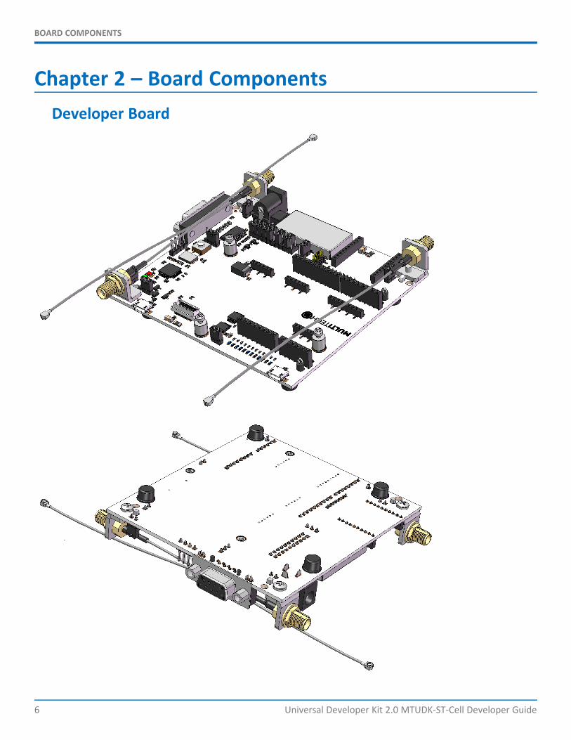
Chapter 2 – Board ComponentsDeveloper Board

BOARD COMPONENTS
Universal Developer Kit 2.0 MTUDK-ST-Cell Developer Guide 7
Developer Board Connectors
Board Components
Label Description
VoltageSelector
Selects between the on-board 3.3V or 5V regulator for powering a SocketModem or mDotFactory default operating voltage is 5V.
J4 RS-232 DB- Serial Connector.
J5 SMC-USB Connector.
J6 USB connection for mbed, serial, and SocketModem. For the MTQ use USB connector on theMTQ. For information on connecting to and using mbed, refer to the device guide for your MTQmodel. (Not available for SocketModems.)
J7 QuickConnect Socket.
JP98 Serial Disconnect Header.
JP197 J-Link Header.
S1 Reset Button. Use to reset the processor of the device attached to the board.
BOARD COMPONENTS
8 Universal Developer Kit 2.0 MTUDK-ST-Cell Developer Guide
Label Description
X2 SocketModem, USB Connector.
X3 SocketModem, GPIO (not connected).
X4 SocketModem Serial Connector.
X5 SocketModem Power Connector.
X6 Arduino Shield Connector.
X7 Arduino Shield Connector.
X8 Arduino Shield Connector.
X9 Arduino Shield Connector.
X10 MTDOT Connector.
X11 MTDOT Connector.
J12 MTDOT Programming Header.
CAUTION: Take care when connecting or disconnecting USB cables to avoid detaching the connector from theboard.
LED Indicators
Label LED Location
STAT LED1 Same side as RS-232 DB-9 connector
COM LED2 Same side as RS-232 DB-9 connector
D7 LED3 Above the SMC-USB connector
D4 LED4 Above the SMC-USB connector
D5 LED5 Above the SMC-USB connector
D8 LED6 Above the SMC-USB connector
D6 LED7 Above the SMC-USB connector
D3 LED8 Above the SMC-USB connector
D0 LED9 Above the SMC-USB connector
D1 LED10 Above the SMC-USB connector
LS LED11 Above the SMC-USB connector
RST LED12 Above the SMC-USB connector
PWR LED13 Above the SMC-USB connector
D2 LED14 Above the SMC-USB connector

INSTALLATION AND OPERATION
Universal Developer Kit 2.0 MTUDK-ST-Cell Developer Guide 9
Chapter 3 – Installation and OperationInstalling a SIM CardInstalling a SIM Card on a SocketModem
Note: When using the SocketModem with a developer board, mount the SocketModem on the developer boardbefore installing the SIM card.
To install the SIM Card:
With the contact side facing down, align the notched edge as outlined on the SocketModem and slide theSIM card completely into the SIM holder.
Installing a SIM Card on a DragonFly
Note: When using the Dragonfly with a developer board, install the SIM card before mounting the Dragonfly onthe developer board.
To install the SIM card:
With the contact side facing down, align the notched edge as shown on the Dragonfly’s SIM holder and slidethe SIM card completely into the SIM holder.
INSTALLATION AND OPERATION
10 Universal Developer Kit 2.0 MTUDK-ST-Cell Developer Guide
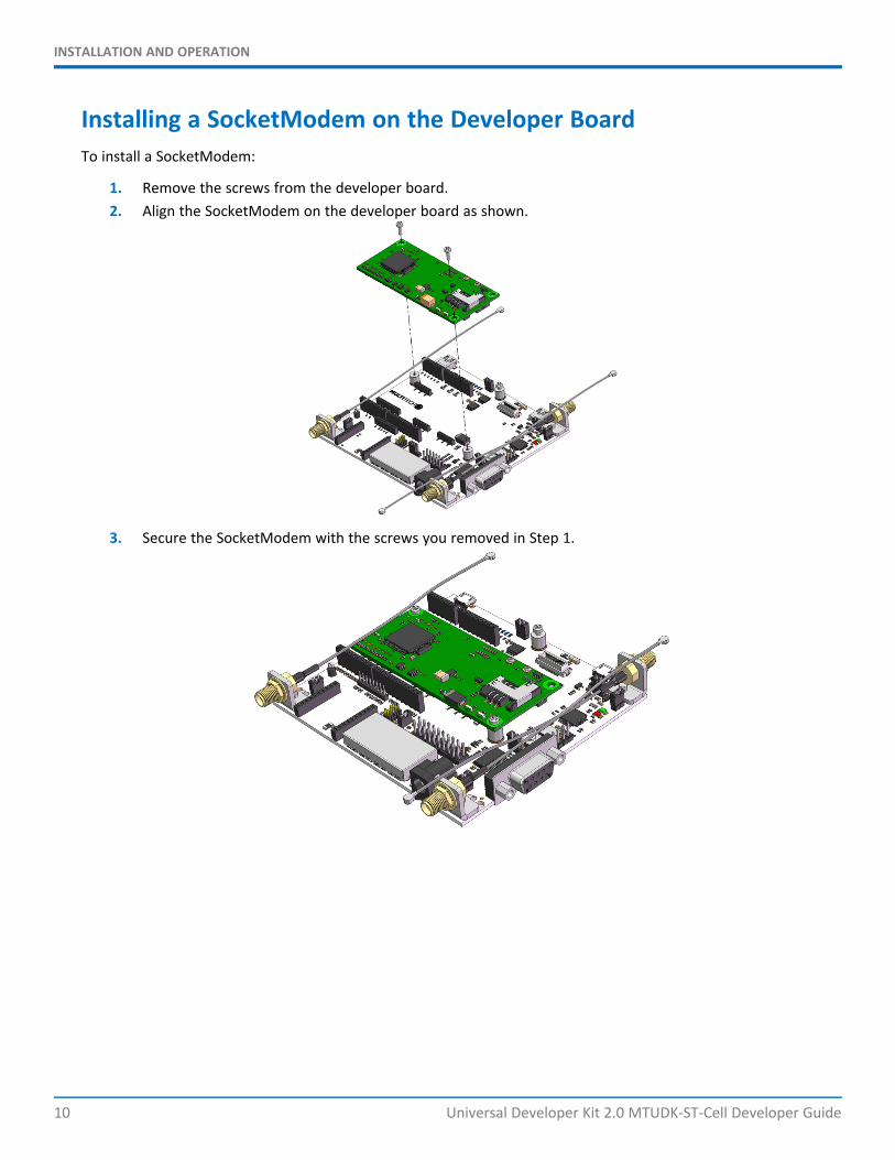
Installing a SocketModem on the Developer BoardTo install a SocketModem:
1. Remove the screws from the developer board.2. Align the SocketModem on the developer board as shown.
3. Secure the SocketModem with the screws you removed in Step 1.
INSTALLATION AND OPERATION
Universal Developer Kit 2.0 MTUDK-ST-Cell Developer Guide 11
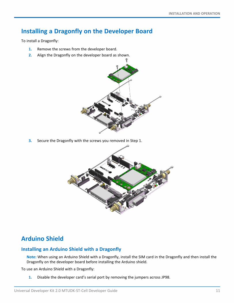
Installing a Dragonfly on the Developer BoardTo install a Dragonfly:
1. Remove the screws from the developer board.2. Align the Dragonfly on the developer board as shown.
3. Secure the Dragonfly with the screws you removed in Step 1.
Arduino ShieldInstalling an Arduino Shield with a Dragonfly
Note: When using an Arduino Shield with a Dragonfly, install the SIM card in the Dragonfly and then install theDragonfly on the developer board before installing the Arduino shield.
To use an Arduino Shield with a Dragonfly:
1. Disable the developer card’s serial port by removing the jumpers across JP98.
INSTALLATION AND OPERATION
12 Universal Developer Kit 2.0 MTUDK-ST-Cell Developer Guide
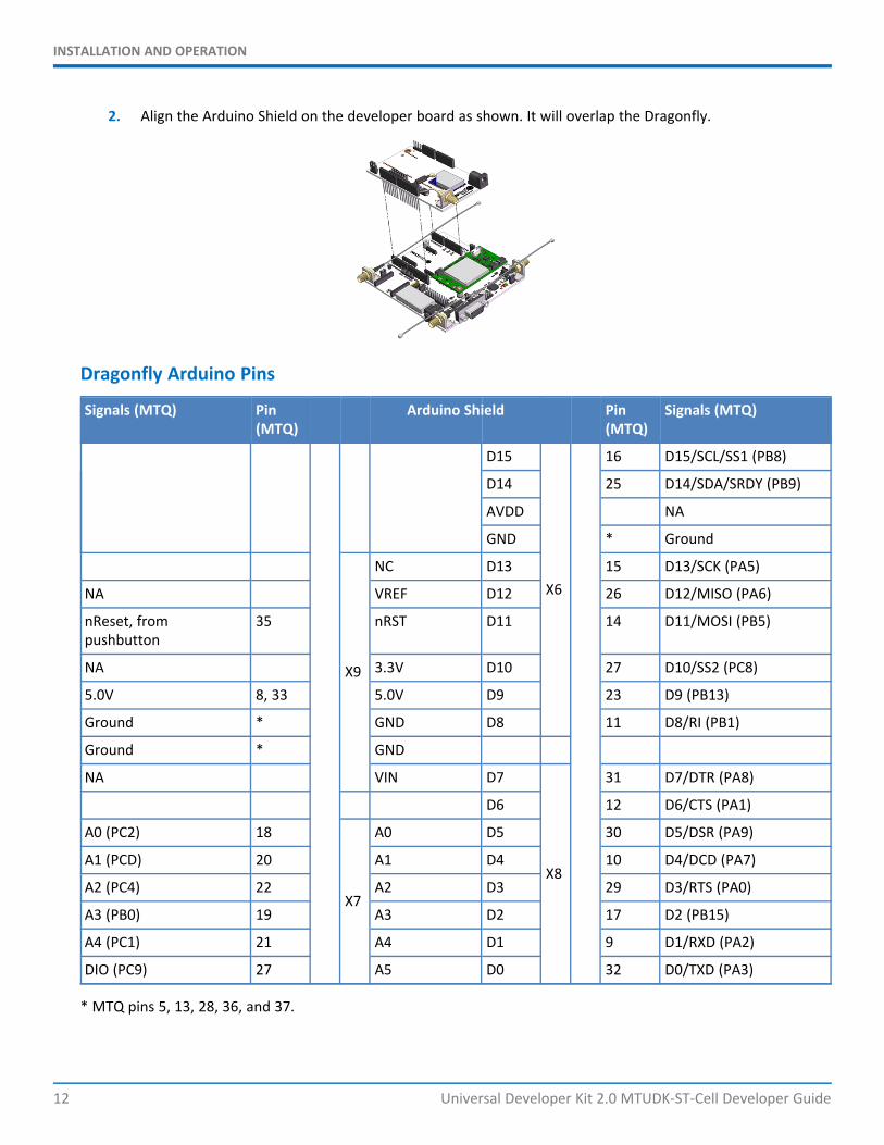
2. Align the Arduino Shield on the developer board as shown. It will overlap the Dragonfly.
Dragonfly Arduino Pins
Signals (MTQ) Pin(MTQ)
Arduino Shield Pin(MTQ)
Signals (MTQ)
D15
X6
16 D15/SCL/SS1 (PB8)
D14 25 D14/SDA/SRDY (PB9)
AVDD NA
GND * Ground
X9
NC D13 15 D13/SCK (PA5)
NA VREF D12 26 D12/MISO (PA6)
nReset, frompushbutton
35 nRST D11 14 D11/MOSI (PB5)
NA 3.3V D10 27 D10/SS2 (PC8)
5.0V 8, 33 5.0V D9 23 D9 (PB13)
Ground * GND D8 11 D8/RI (PB1)
Ground * GND
NA VIN D7
X8
31 D7/DTR (PA8)
D6 12 D6/CTS (PA1)
A0 (PC2) 18
X7
A0 D5 30 D5/DSR (PA9)
A1 (PCD) 20 A1 D4 10 D4/DCD (PA7)
A2 (PC4) 22 A2 D3 29 D3/RTS (PA0)
A3 (PB0) 19 A3 D2 17 D2 (PB15)
A4 (PC1) 21 A4 D1 9 D1/RXD (PA2)
DIO (PC9) 27 A5 D0 32 D0/TXD (PA3)
* MTQ pins 5, 13, 28, 36, and 37.
INSTALLATION AND OPERATION
Universal Developer Kit 2.0 MTUDK-ST-Cell Developer Guide 13
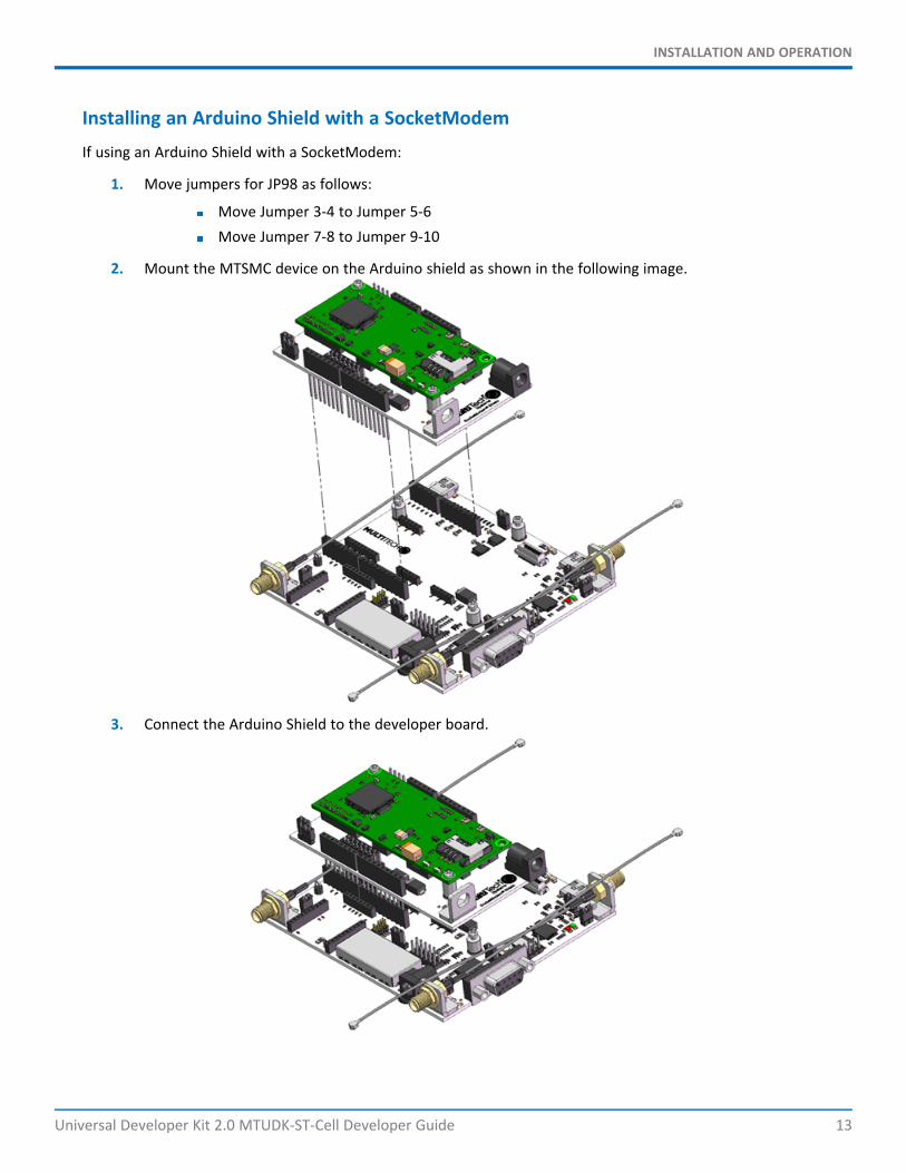
Installing an Arduino Shield with a SocketModem
If using an Arduino Shield with a SocketModem:
1. Move jumpers for JP98 as follows:
Move Jumper 3-4 to Jumper 5-6Move Jumper 7-8 to Jumper 9-10
2. Mount the MTSMC device on the Arduino shield as shown in the following image.
3. Connect the Arduino Shield to the developer board.
INSTALLATION AND OPERATION
14 Universal Developer Kit 2.0 MTUDK-ST-Cell Developer Guide
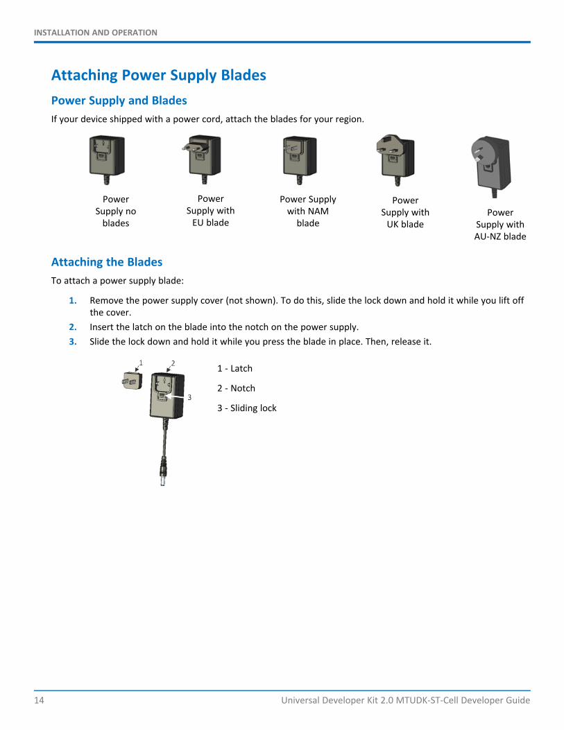
Attaching Power Supply BladesPower Supply and BladesIf your device shipped with a power cord, attach the blades for your region.
PowerSupply no
blades
PowerSupply with
EU blade
Power Supplywith NAM
blade
PowerSupply with
UK bladePower
Supply withAU-NZ blade
Attaching the BladesTo attach a power supply blade:
1. Remove the power supply cover (not shown). To do this, slide the lock down and hold it while you lift offthe cover.
2. Insert the latch on the blade into the notch on the power supply.3. Slide the lock down and hold it while you press the blade in place. Then, release it.
1 - Latch
2 - Notch
3 - Sliding lock
INSTALLATION AND OPERATION
Universal Developer Kit 2.0 MTUDK-ST-Cell Developer Guide 15
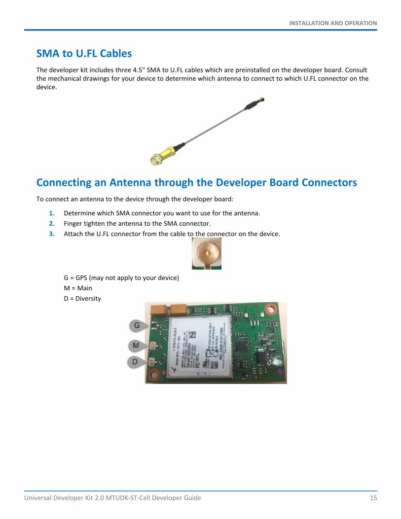
SMA to U.FL CablesThe developer kit includes three 4.5" SMA to U.FL cables which are preinstalled on the developer board. Consultthe mechanical drawings for your device to determine which antenna to connect to which U.FL connector on thedevice.
Connecting an Antenna through the Developer Board ConnectorsTo connect an antenna to the device through the developer board:
1. Determine which SMA connector you want to use for the antenna.2. Finger tighten the antenna to the SMA connector.3. Attach the U.FL connector from the cable to the connector on the device.
G = GPS (may not apply to your device)M = MainD = Diversity
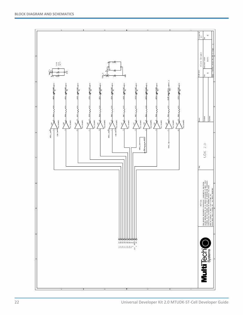
BLOCK DIAGRAM AND SCHEMATICS
16 Universal Developer Kit 2.0 MTUDK-ST-Cell Developer Guide
Chapter 4 – Block Diagram and Schematics
BLOCK DIAGRAM AND SCHEMATICS
Universal Developer Kit 2.0 MTUDK-ST-Cell Developer Guide 17
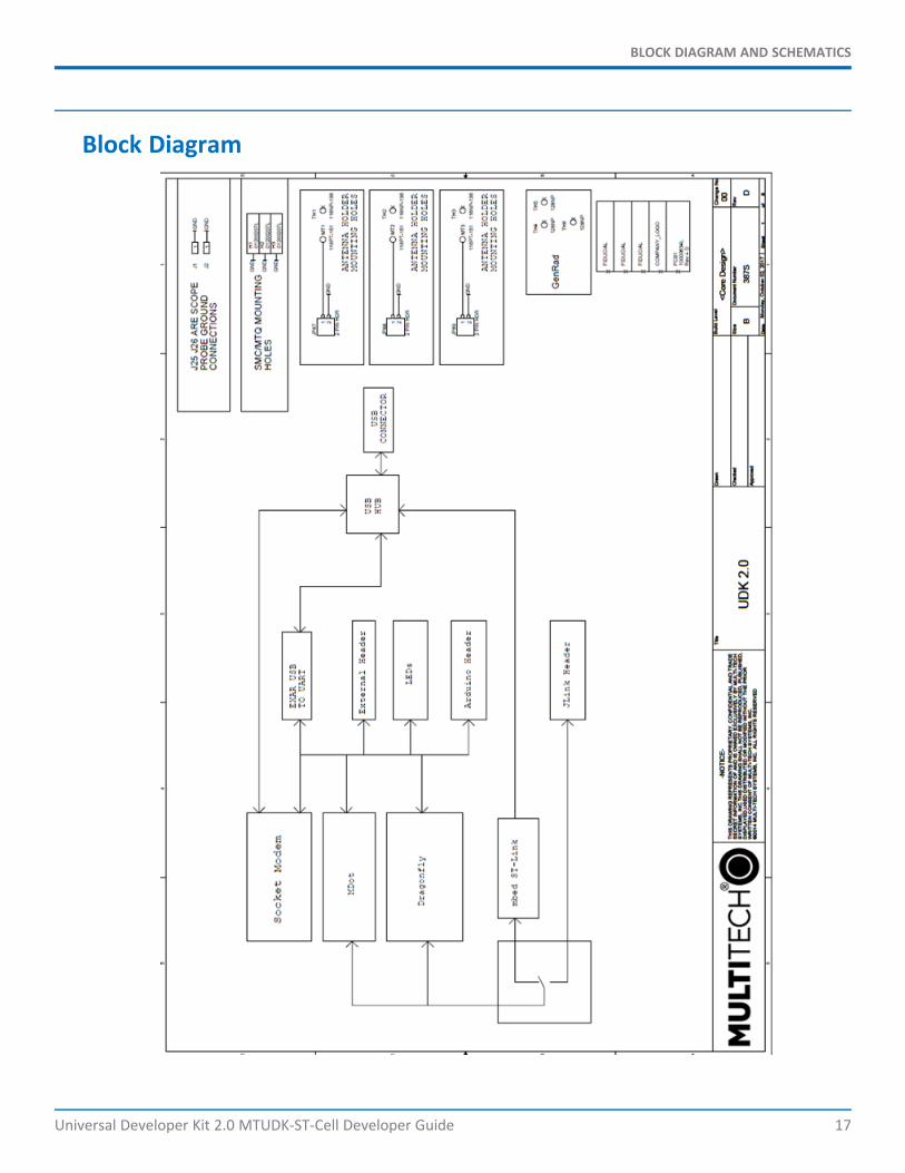
Block Diagram
BLOCK DIAGRAM AND SCHEMATICS
18 Universal Developer Kit 2.0 MTUDK-ST-Cell Developer Guide
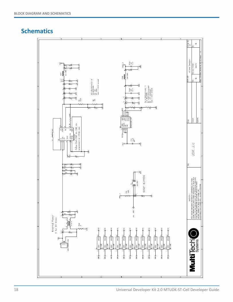
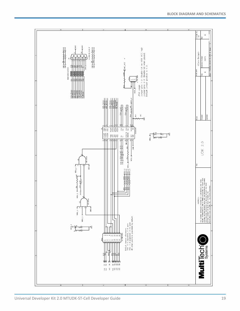
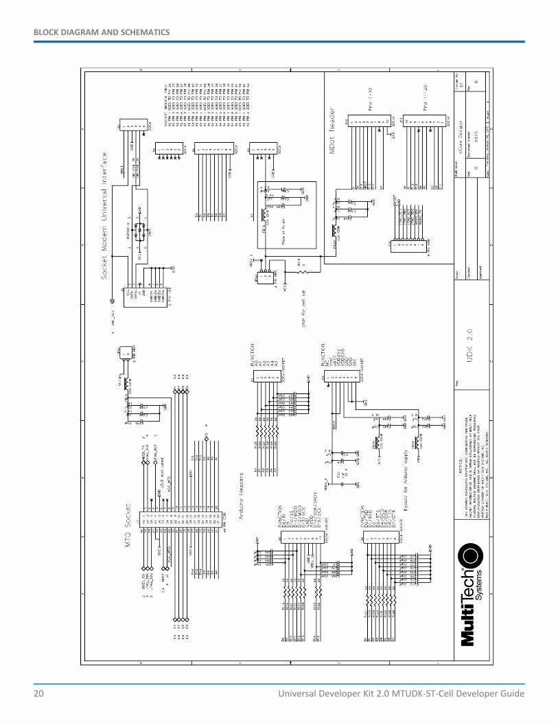
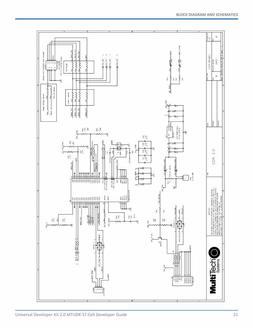
Schematics
BLOCK DIAGRAM AND SCHEMATICS
Universal Developer Kit 2.0 MTUDK-ST-Cell Developer Guide 19
BLOCK DIAGRAM AND SCHEMATICS
20 Universal Developer Kit 2.0 MTUDK-ST-Cell Developer Guide
BLOCK DIAGRAM AND SCHEMATICS
Universal Developer Kit 2.0 MTUDK-ST-Cell Developer Guide 21
BLOCK DIAGRAM AND SCHEMATICS
22 Universal Developer Kit 2.0 MTUDK-ST-Cell Developer Guide
DESIGN CONSIDERATIONS
Universal Developer Kit 2.0 MTUDK-ST-Cell Developer Guide 23
Chapter 5 – Design ConsiderationsNoise Suppression DesignAdhere to engineering noise-suppression practices when designing a printed circuit board (PCB). Noise suppressionis essential to the proper operation and performance of the modem and surrounding equipment.
Any OEM board design must consider both on-board and off-board generated noise that can affect digital signalprocessing. Both on-board and off-board generated noise that is coupled on-board can affect interface signal levelsand quality. Noise in frequency ranges that affect modem performance is of particular concern.
On-board generated electromagnetic interference (EMI) noise that can be radiated or conducted off-board isequally important. This type of noise can affect the operation of surrounding equipment. Most local governmentagencies have certification requirements that must be met for use in specific environments.
Proper PC board layout (component placement, signal routing, trace thickness and geometry, and so on)component selection (composition, value, and tolerance), interface connections, and shielding are required for theboard design to achieve desired modem performance and to attain EMI certification.
Other aspects of proper noise-suppression engineering practices are beyond the scope of this guide. Consult noisesuppression techniques described in technical publications and journals, electronics and electrical engineering textbooks, and component supplier application notes.
PC Board Layout GuidelineIn a 4-layer design, provide adequate ground plane covering the entire board. In 4-layer designs, power and groundare typically on the inner layers. Ensure that all power and ground traces are 0.05 inches wide.
The recommended hole size for the device pins is 0.036 in. +/-0.003 in. in diameter. Use spacers to hold the devicevertically in place during the wave solder process.
Electromagnetic InterferenceThe following guidelines are offered specifically to help minimize EMI generation. Some of these guidelines are thesame as, or similar to, the general guidelines. To minimize the contribution of device-based design to EMI, youmust understand the major sources of EMI and how to reduce them to acceptable levels.
Keep traces carrying high frequency signals as short as possible.Provide a good ground plane or grid. In some cases, a multilayer board may be required with full layers forground and power distribution.Decouple power from ground with decoupling capacitors as close to the device's power pins as possible.Eliminate ground loops, which are unexpected current return paths to the power source and ground.Decouple the telephone line cables at the telephone line jacks. Typically, use a combination of seriesinductors, common mode chokes, and shunt capacitors. Methods to decouple telephone lines are similar todecoupling power lines; however, telephone line decoupling may be more difficult and deserves additionalattention. A commonly used design aid is to place footprints for these components and populate asnecessary during performance/EMI testing and certification.Decouple the power cord at the power cord interface with decoupling capacitors. Methods to decouplepower lines are similar to decoupling telephone lines.
DESIGN CONSIDERATIONS
24 Universal Developer Kit 2.0 MTUDK-ST-Cell Developer Guide
Locate high frequency circuits in a separate area to minimize capacitive coupling to other circuits.Locate cables and connectors to avoid coupling from high frequency circuits.Lay out the highest frequency signal traces next to the ground grid.If using a multilayer board design, make no cuts in the ground or power planes and be sure the groundplane covers all traces.Minimize the number of through-hole connections on traces carrying high frequency signals.Avoid right angle turns on high frequency traces. Forty-five degree corners are good; however, radius turnsare better.On 2-layer boards with no ground grid, provide a shadow ground trace on the opposite side of the board totraces carrying high frequency signals. This will be effective as a high frequency ground return if it is threetimes the width of the signal traces.Distribute high frequency signals continuously on a single trace rather than several traces radiating fromone point.
Electrostatic Discharge ControlHandle all electronic devices with precautions to avoid damage due to the static charge accumulation.
See the ANSI/ESD Association Standard (ANSI/ESD S20.20-1999) – a document “for the Development of anElectrostatic Discharge Control for Protection of Electrical and Electronic Parts, Assemblies and Equipment.” Thisdocument covers ESD Control Program Administrative Requirements, ESD Training, ESD Control Program PlanTechnical Requirements (grounding/bonding systems, personnel grooming, protected areas, packaging, marking,equipment, and handling), and Sensitivity Testing.
MultiTech strives to follow these recommendations. Input protection circuitry is incorporated in MultiTech devicesto minimize the effect of static buildup. Take precautions to avoid exposure to electrostatic discharge duringhandling.
MultiTech uses and recommends that others use anti-static boxes that create a faraday cage (packaging designedto exclude electromagnetic fields). MultiTech recommends that you use our packaging when returning a productand when you ship your products to your customers.
USB DesignMultiTech recommends that you review Intel's High Speed USB Platform Design Guidelines for information aboutUSB signal routing, impedance, and layer stacking. Also:
Shield USB cables with twisted pairs (especially those containing D+/D-).Use a single 5V power supply for USB devices. See Power Draw for current (ampere) requirements.Route D+/D- together in parallel with the trace spacing needed to achieve 90 ohms differential impedancefor the USB pair and to maintain a 20 mil space from the USB pair and all other signals.If power is provided externally, use a common ground between the carrier board and the device.