Embed Size (px)
Citation preview
MTRX 2700 labnotes.doc
MTRX 2700 – Mechatronics 2
Laboratory Notes The laboratory sessions are very important in MTRX 2700. It is during these sessions that you will work to put into practice what you have heard in the lectures and read up by yourself. The laboratory work will begin with three self-contained laboratory exercises. You must prepare for each exercise before the lab session, and aim to complete each one in the time allocated. Following the successful completion of these exercises, students will be given a major assignment, which will take 4 three hour laboratory sessions to complete.
Lab Organisation Location: Mechatronics Lab, Room 325 in the Link Building Labs Begin: Week 3 Tutors: See the Unit of Study Outline
Lab Groups All lab work in MTRX 2700 will be in groups of two. Laboratory partners and workstations will be allocated by the lecturer, and cannot be changed. Lab partners will be notified on the noticeboard at the front of the lab.
Lab Notebooks You will need to purchase a bound hardcover A4 notebook for use in the laboratory sessions. You will record all details of the experiments, including your programs, comments, results etc. in the lab notebook. The purpose of the laboratory notebook is to document the experiment to a level of detail such that another person could replicate your results from the information recorded in the notebook. Include in your notebook all failed attempts, as well as successes. Knowledge of how not to do things is just as important as how to do them. The notebooks are assessable! Please refer to Appendix A of these notes for guidelines on good lab notebook practise.
Lab Rules/Code of Conduct The lab rules and code of conduct are displayed on the noticeboard in the lab. Take the time to familiarise yourself with the rules. They are also available on-line at http://www.acfr.usyd.edu.au/teaching/mx-lab/ .
Lab Equipment Your group will be allocated to a work station in the Mechatronics Lab. Each workstation has the basic equipment that you will be using during the laboratory sessions:
scheding Page 1 17/07/2007

MTRX 2700 labnotes.doc
• An EVBPlus MC68HC11 evaluation/development board, from www.evbplus.com ;
• A PC with software to interface to the development board; • A power supply for the MC68HC11 board and other circuits; • A digital oscilloscope; • A toolkit (which includes the oscilloscope probes).
Please be aware that to obtain a toolkit, you must ask one of the tutors to get it for you. You must exchange your student card for the toolkit. The student card will be returned to you when the complete toolkit is returned to the tutor.
scheding Page 2 17/07/2007

MTRX 2700 labnotes.doc
Appendix A: Good Lab Book Practises From IP Australia: http://www.ipaustralia.gov.au/ipprofessor/a/goodpractices.pdf
scheding Page 3 17/07/2007

Practise GoodLab Book PracticesGood Lab Book Practice for Researchers
Why is a LaboratoryNotebook so important?
A laboratory notebook is a complete legal document recording your work inthe laboratory. Laboratory notebooks are vital in proving that you conductedthe research. A properly kept laboratory notebook is invaluable in proving theright to own a related patent in Australia, or obtain one in the United States(where patent rights are assigned on a 'first to invent' basis, rather than the'first to file' system that applies in Australia). One of the most effectivemethods to prove you were the 'first to invent' something is via a well-keptlaboratory notebook. This short guide is designed to help you practice goodlaboratory notebook practices.
Electronic laboratory notebooks are becoming more widely used, butelectronic records are not currently as effective as evidence of invention.At present, paper-based records are preferred as they cannot be easily altered,this is likely to change in the future however. Any electronic records should beprinted out and affixed in your laboratory notebook.
If you are unsure, or need further guidance, seek legal advice or contact youruniversity or employer's IP officer or Research Office.
See over for a checkl ist of i tems your laboratory notebook should inc lude ➔
Where can I getmore information?
IP Australia is the Federal Government Agency responsible for theregistration of patents, trade marks and designs. IP Australia hasspecifically developed an online resource, IP Professor, for thetertiary sector. IP Professor features online lecture notes, request-a-lecturer, an IP news clipping service and case studies for useby the tertiary sector. For further information, visit our websitewww.ipaustralia.gov.au and select the IP Professor logo or phone02 6283 2999.
If you would like to order additional copiesof this help guide, please request via email:[email protected]

1
2
2
3
4
4
5
5
6
7
8
9
10
11
12
12
13
14
15
Pages that are permanently sewn or otherwise bound to the book. There should be no loosepages of paper - all data should be entered directly into your laboratory book (see point 9);
Pages that are numbered consecutively;
Legible entries in ink (preferably black). Large white spaces should not be left in the text. Such spaces should be lined through to avoid misinterpretation;
Any errors remaining legible, for example, lined out (sleep) rather than erased or covered. If necessary (ie the reason for the alteration is not obvious), a reason for the alterationshould be given. This is to avoid suspicion of concealment;
Any changes and additions signed and dated by you;
Details recorded of any pre-experimental work concluded in relation to the project,including details of any ideas generated during thinking/discussion sessions with co-workers;
Entries in chronological order, without blank pages. To start an entry on a new page, draw a line through any unused portion of the previous page. Never tear out or destroy pages;
Results obtained at a later stage recorded in date order and cross referencedto earlier entry;
Additional information, including electronic records, such as result print outs, diagrams and photographs dated and attached via stapling or adhesive. These should be signed and dated by you across the document and the underlying page;
All non-standard terms, processes and abbreviations defined;
A record of equipment details including manufacturer, model and serial number and indicate the purpose if not clear;
A sketch of the equipment set-up used, noting any variations to the procedure;
No value judgements regarding your perception of the protectability of the research;
The conclusion of each work period or experiment signed and dated by you, andsigned off by a witness. The witness should be knowledgable in your area ofresearch but not directly participating in your project; and
Duplicate copies made and kept secure at a separate location. Ensure that nounauthorised persons have access to your notebooks to preserve their confidentiality.
Your Laboratory Notebook Should Have:
www.ipaustralia.gov.au
Do not be frightened to write too much! Your laboratory notebook should be a complete record of what has been done. Any methods used must be clearly described, noting any unusual delays or occurrences. Any person knowledgable in your area of study should understand the procedures used to arrive at the result. Remember, the more details you include, the better chance you will have of successfully proving you were the 'first to invent' if someone else tries to patent your invention in the United States.

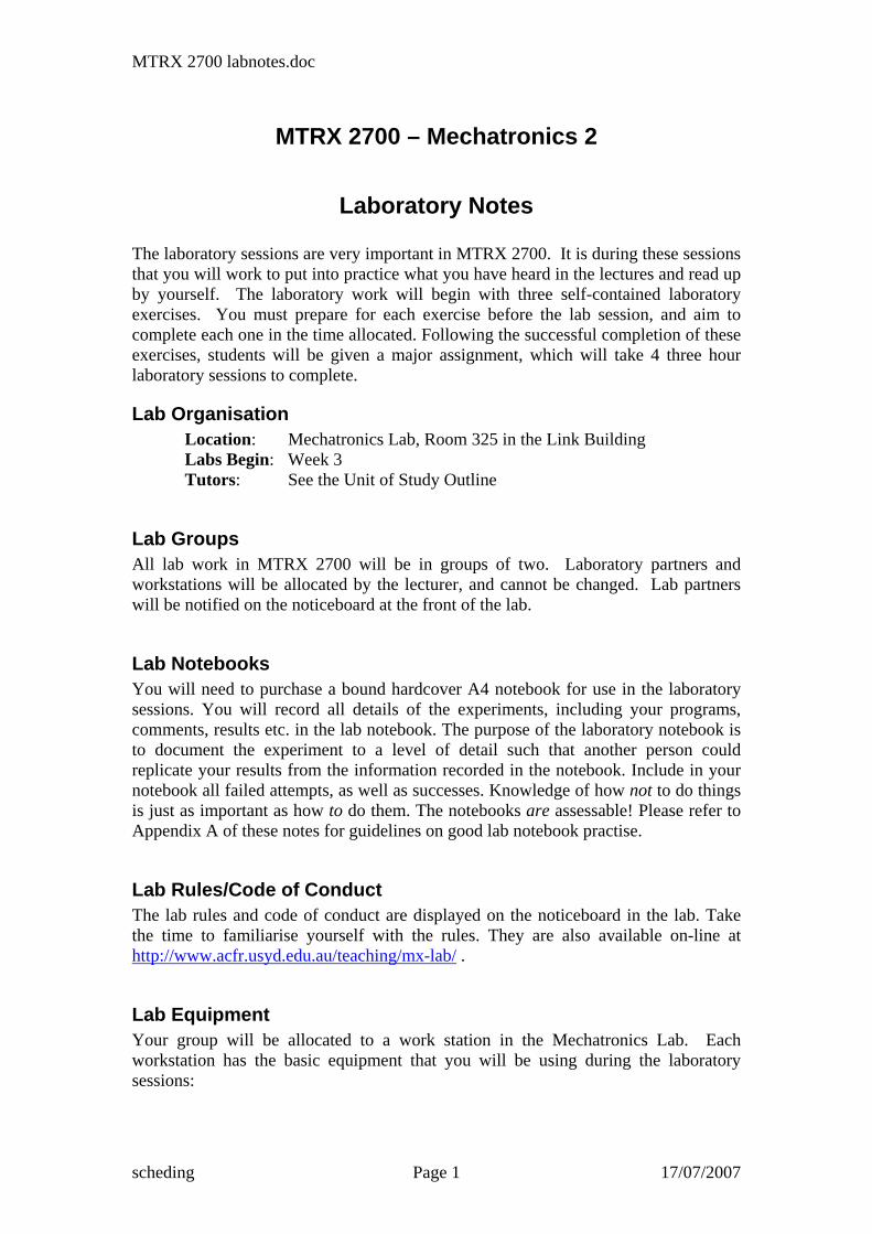
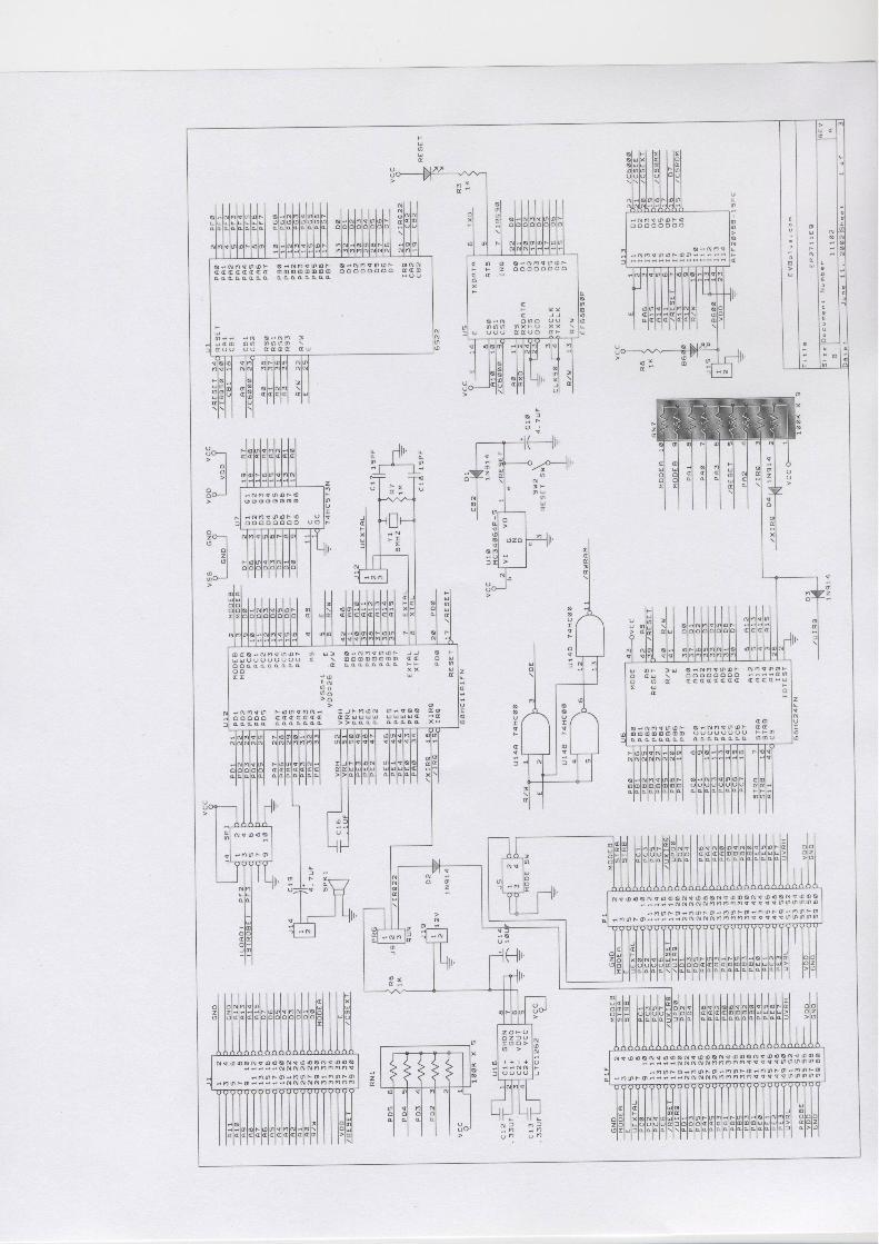
MTRX 2700 labnotes.doc
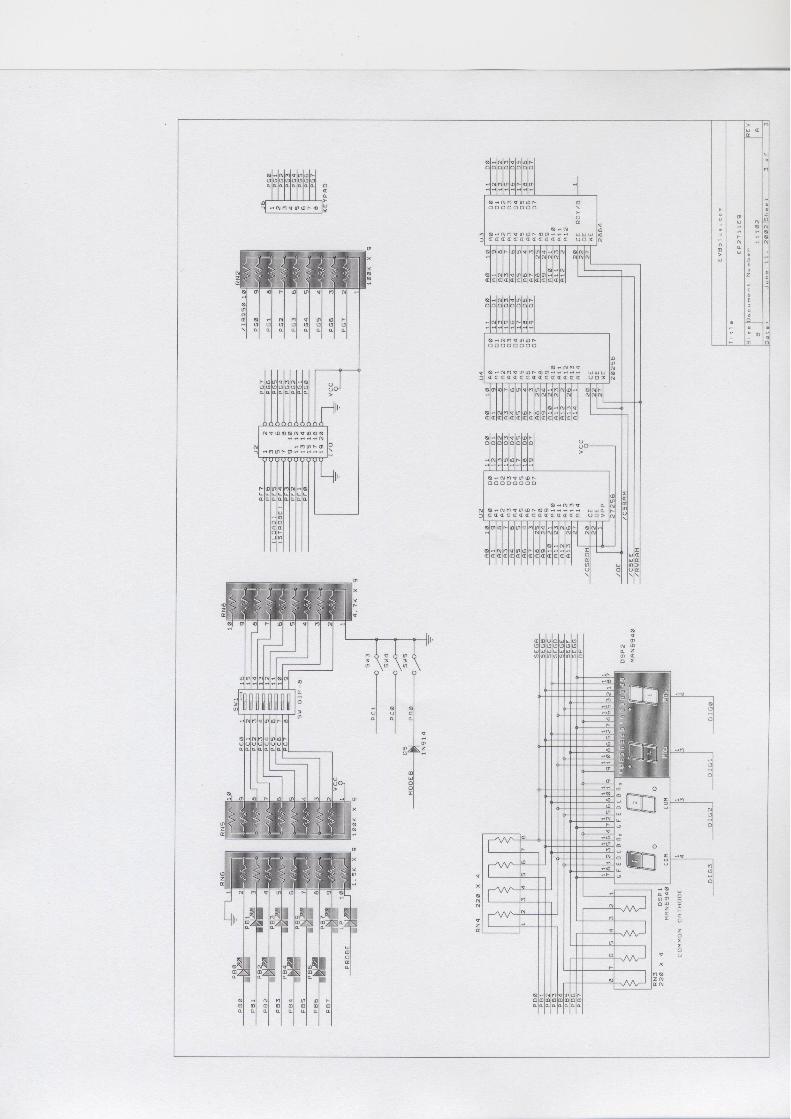
Appendix B: EVBPlus2 Board Schematic From: http://www.evbplus.com/
scheding Page 4 17/07/2007
MTRX 2700 labnotes.doc
Appendix C: EVBPlus2 Board Documentation From: http://www.evbplus.com/
EVBplus2 68HC11 Development Board
Getting Started Manual
Version 1.00 The Ep2711E9, a low cost and high performance development board, provides real time emulation for the Motorola 68HC11microcontroller E family. It offers all useful features of the Motorola EVB board with the Buffalo monitor and adds numerous enhancements at an extremely low cost. It combines a complete 68HC11 development system, an advanced trainer, a reliable 711E9 programmer and a versatile SBC into one package. For engineers, it’s a WICE in-circuit emulator development system and Motorola EVB, EVM, EVS replacement, a convenient prototype platform, and a low cost single board computer. For students, it’s a user-friendly microcontroller trainer. It is as powerful as a high priced real-time in-circuit emulator, but it’s affordable as a low cost single board computer.
Ep2711E9 includes user-friendly IDE software which runs under Windows® 95, 98, 2000 and XP. It offers fast file transfer, single-stepping, breakpoints, data watch for memory and registers, symbolic debugging compatibility with most assemblers and compilers, and user program termination with the <Esc> key. Our exclusive phantom monitor™ technology preserves all interrupt vectors including RESET and All on-chip RAM ($00-$1FF), EEPROM, and 30K external emulation RAM ($8800-$FFFF) available for user applications - there is no pre-empted chip memory. The hardware includes a prototype area, 16 extra I/O ports F and G, one logic probe, on board 16X2 LCD display with backlight, 4x4 keypad connector, 8 sensor I/O port, SPI port, speaker, 4-digit LED display, potentiometer, 8 LED status indicators for port B, one 8 position DIP switch connected to port C and three pushbutton switches, dual UART, RS485 interface, IR transceiver with on-board 38 KHz OSC, on-board 12 programming voltage supply and 60-pin EVB/EVBU-compatible connector. The package also includes a 7.5V 300mA wall plug-in power supply and a 6-foot DB9 cable. The specification of the AC adapter is: DC output: 7.5V to 9V Current rating: 300 mA to 1A Type of plug: 2.1mm female barrier plug, center positive In Robot applications, if more power is needed, the user can upgrade the AC adapter to 9V 500MA or 9V 1A, otherwise the board could reset itself when the VCC drops below 4.75V.
scheding Page 5 17/07/2007
MTRX 2700 labnotes.doc
GETTING STARTED
To operate the Ep2711E9 board, follow steps1 through 6 below:
Step 1.
Plug the AC adapter into a wall outlet, and plug the DC plug at the other end into the DC jack on the lower right side of the Ep2711E9 board. During the initial power up, the reset LED should blink 4 times. If not, turn over to the Questions & Answers section of the user manual.
Step 2.
Plug the DB9 male end of the cable into the DB9 connector P2 on the upper right side of the Ep2711E9 board, and plug the DB9 female end of the cable to the COM1 or COM2 port on the back of the PC. The DB9 connector P3 on the lower right side of the board is the 68HC11 SCI port that can be used by user’s program.
Step 3.
Press the reset button on the Ep2711E9 board, and the reset LED, which is located above the switch, should now blink only twice. If not, turn over to the Questions & Answers section of the user manual.
Step 4.
Insert the EVBplus2 6811 CD in a CD drive, and run the “SETUP.BAT” on the CDROM. You can use the explorer to find the batch file, and then double click it to run. If you have problems to install software under Windows2000, you need to download the Microsoft Windows 2000 service pack 2 from Microsoft web site to upgrade your system.
Step 5.
After software is successfully installed, run the EVBplus2 program.
Step 6.
Configure your system to provide the default working directory, the file name, the COM port number, and the micro type. If the working directory is C:\Ep2IDE\examples, COM port is set correctly and the file name is TEST, you can click the DEBUG button on the screen, the system will automatically down load the test program TEST.s19.
At the prompt Ep6811>, enter go \start
It will run the TEST program in real time. The program will test the switches, scan keypad, send message to the LCD display, emulate an IR proximity sensor, adjust the LED display brightness, generate music and shift number 0 to F on the seven-segment display. If you stop the program, the speaker will generate a click noise, because the output comparator is still interrupting the 68HC11. To stop the clicking noise, you can press the reset button once.
scheding Page 6 17/07/2007
MTRX 2700 labnotes.doc
SOFTWARE DEVELOPMENT
The steps to create your source code as follows:
1 Click the CONFIGURE button to specify the current working directory. This is the first step that you must do. All other commands will automatically access this directory as the default directory. Secondly you must specify the file name, the COM port number, and the micro type. Finally SAVE it before exit.
2. Click the EDIT button and it will bring up the freeware EDIT that comes with your computer. If your source file name does not exist in the working directory, the Edit screen will be blank; otherwise it will bring up your source code. The file name must not be longer than 8 characters because the EDIT will only recognize up to 8 characters in file name.
The memory locations from $00-$1FF ($00-$FF for A family) are available as the user DATA RAM. The EVBplus2 board does not use RAM locations at $40-$FF, as the BUFFALO monitor does. The 30K memory locations from $8800 to $FFFF are available to the user program CODE. In assembly language, you specify the starting address by the ORG statement.
You can start DATA RAM at address $00 with the statement ORG 0 followed by RAM variables, such as:
ORG 0
TEMP: RMB 1 ; reserve one byte of RAM for temp storage
XTEMP: RMB 2 ; reserve two bytes of RAM for temp storage
If your program is small, less that 4K, you can start your program at address $F000 with the statement ORG $F000 followed by your program, such as:
ORG $F000
LDS #$FF ; the top of the 68HC11A1 internal RAM
JSR INIT_IO ; initialize I/O ports
For a good programming practice, you should make the first line of your code with the LDS instruction.
It will assemble your program code in 4K locations from $F000 to $FFFF. If your program is larger, you can change the ORG $F000 to ORG $E000, or ORG $D000. When you finish your debugging, you do not have to relocate your code and re-assemble it again. Your code is final for stand-alone operation after you finish the debugging, it works just like a real time In-Circuit Emulator..
The Ep2711E9 board can stop your program if it’s hung in a loop, when you press the ESC key at the PC keyboard. It will interrupt the Ep2711E9, but the BUFFALO monitor can’t stop the program unless you reset the system. The problem with resetting the system is that you would not know where the 68HC11 was hung.
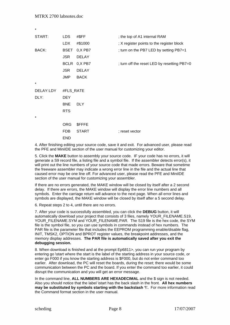
Here is a very simple program, but it’s complete. The program source code is similar to the tutor2.asm in the directory c:\Ep2IDE\examples. It will flash the PB7 LED when it’s running.
PB7: EQU $80 ; bit 7 of port B
FLS_RATE: EQU $8B00 ; change this number will change LED flash rate
ORG $F000
scheding Page 7 17/07/2007
MTRX 2700 labnotes.doc
*
START: LDS #$FF ; the top of A1 internal RAM
LDX #$1000 ; X register points to the register block
BACK: BSET 0,X PB7 ; turn on the PB7 LED by setting PB7=1
JSR DELAY
BCLR 0,X PB7 ; turn off the reset LED by resetting PB7=0
JSR DELAY
JMP BACK
*
DELAY: LDY #FLS_RATE
DLY: DEY
BNE DLY
RTS
*
ORG $FFFE
FDB START ; reset vector
END
4. After finishing editing your source code, save it and exit. For advanced user, please read the PFE and MiniIDE section of the user manual for customizing your editor.
5. Click the MAKE button to assembly your source code. IF your code has no errors, it will generate a S9 record file, a listing file and a symbol file. If the assembler detects error(s), it will print out the line numbers of your source code that made errors. Beware that sometime the freeware assembler may indicate a wrong error line in the file and the actual line that caused error may be one line off. For advanced user, please read the PFE and MiniIDE section of the user manual for customizing your assembler.
If there are no errors generated, the MAKE window will be closed by itself after a 2 second delay. If there are errors, the MAKE window will display the error line numbers and all symbols. Enter the carriage return will advance to the next page. When all error lines and symbols are displayed, the MAKE window will be closed by itself after a 5 second delay.
6. Repeat steps 2 to 4, until there are no errors.
7. After your code is successfully assembled, you can click the DEBUG button, it will automatically download your project that consists of 3 files, namely YOUR_FILENAME.S19, YOUR_FILENAME.SYM and YOUR_FILENAME.PAR. The S19 file is the hex code, the SYM file is the symbol file, so you can use symbols in commands instead of hex numbers. The PAR file is the parameter file that includes the EEPROM programming enable/disable flag, INIT, TMSK2, OPTION and BPROT register values, the breakpoint addresses, and the memory display addresses. The PAR file is automatically saved after you exit the debugging session.
8. When download is finished and at the prompt Ep6811>, you can run your program by entering go \start where the start is the label of the starting address in your source code, or enter go F000 if you know the starting address is $F000, but do not enter command too earlier. After download, the PC will reset the boards, during the reset; there would be some communication between the PC and the board. If you enter the command too earlier, it could disrupt the communication and you will get an error message.
In the command line, ALL NUMBERS ARE HEXADECIMAL and the $ sign is not needed. Also you should notice that the label \start has the back slash in the front. All hex numbers may be substituted by symbols starting with the backslash ‘\’. For more information read the Command format section in the user manual.
scheding Page 8 17/07/2007
MTRX 2700 labnotes.doc
9. During the debug session, if you want to modify your source code, you don’t have to exit the debugger. You can click the EDIT button to edit your code and save your new code in the same file name, then click the MAKE button to assemble the code. After the new S19 file is generated, click the debug button at the task bar, the bottom line of the screen, to activate the debug window, then enter the F10 key and the R option to download your project and start to debug again.
If you did not close the EDIT window, you don’t have to open a new EDIT window to edit a file. If the editor was minimized at the task bar, just to click it to activate it. Click too many times of the EDIT button without closing it will open up a lot of EDIT windows during the debugging and you don’t know which file is the most recently modified file.
The EDIT and DEBUGGER windows will not be closed automatically. Before clicking the edit or the debugger button, always check at the task bar. If they are already open, just activate them.
10. If you need to program a HC711E9, you can use this board as a HC711E9 programmer. At first, you must make sure that the working directory, file name and the COM port are configured correctly, then click the PROGRAM button to program the HC711E9. The programming is done in the bootstrap mode and the programming instructions will be displayed on the screen step by step. The memory addresses range for the HC711E9 is from $D000 to $FFFF. If your S19 file contains addresses outside of this range, an error message will be generated and the chip will not be programmed. During the programming, the data will be automatically verified.
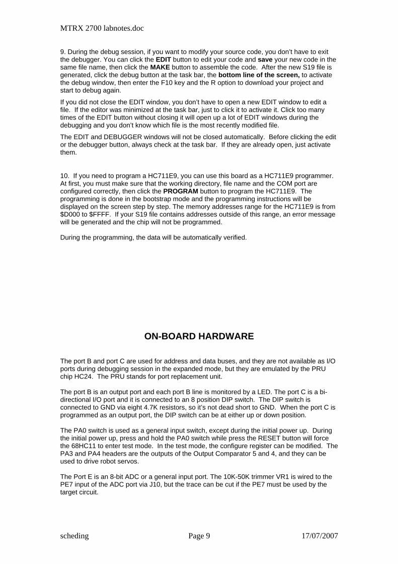
ON-BOARD HARDWARE
The port B and port C are used for address and data buses, and they are not available as I/O ports during debugging session in the expanded mode, but they are emulated by the PRU chip HC24. The PRU stands for port replacement unit. The port B is an output port and each port B line is monitored by a LED. The port C is a bi-directional I/O port and it is connected to an 8 position DIP switch. The DIP switch is connected to GND via eight 4.7K resistors, so it’s not dead short to GND. When the port C is programmed as an output port, the DIP switch can be at either up or down position. The PA0 switch is used as a general input switch, except during the initial power up. During the initial power up, press and hold the PA0 switch while press the RESET button will force the 68HC11 to enter test mode. In the test mode, the configure register can be modified. The PA3 and PA4 headers are the outputs of the Output Comparator 5 and 4, and they can be used to drive robot servos. The Port E is an 8-bit ADC or a general input port. The 10K-50K trimmer VR1 is wired to the PE7 input of the ADC port via J10, but the trace can be cut if the PE7 must be used by the target circuit.
scheding Page 9 17/07/2007
MTRX 2700 labnotes.doc
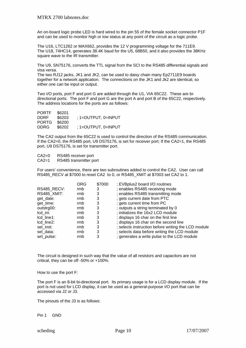
An on-board logic probe LED is hard wired to the pin 55 of the female socket connector P1F and can be used to monitor high or low status at any point of the circuit as a logic probe. The U16, LTC1262 or MAX662, provides the 12 V programming voltage for the 711E9. The U18, 74HC14, generates 38.4K baud for the U5, 68B50, and it also provides the 38KHz square wave to the IR transmitter. The U9, SN75176, converts the TTL signal from the SCI to the RS485 differential signals and visa versa. The two RJ12 jacks, JK1 and JK2, can be used to daisy chain many Ep2711E9 boards together for a network application. The connections on the JK1 and Jk2 are identical, so either one can be input or output. Two I/O ports, port F and port G are added through the U1, VIA 65C22. These are bi-directional ports. The port F and port G are the port A and port B of the 65C22, respectively. The address locations for the ports are as follows: PORTF $6201 DDRF $6203 ; 1=OUTPUT, 0=INPUT PORTG $6200 DDRG $6202 ; 1=OUTPUT, 0=INPUT The CA2 output from the 65C22 is used to control the direction of the RS485 communication. If the CA2=0, the RS485 port, U9 DS75176, is set for receiver port; If the CA2=1, the RS485 port, U9 DS75176, is set for transmitter port. CA2=0 RS485 receiver port CA2=1 RS485 transmitter port For users’ convenience, there are two subroutines added to control the CA2. User can call RS485_RECV at $7000 to reset CA2 to 0, or RS485_XMIT at $7003 set CA2 to 1. ORG $7000 ; EVBplus2 board I/O routines RS485_RECV: rmb 3 ; enables RS485 receiving mode RS485_XMIT: rmb 3 ; enables RS485 transmitting mode get_date: rmb 3 ; gets current date from PTC get_time: rmb 3 ; gets current time from PC outstrg00: rmb 3 ; outputs a string terminated by 0 lcd_ini: rmb 3 ; initializes the 16x2 LCD module lcd_line1: rmb 3 ; displays 16 char on the first line lcd_line2: rmb 3 ; displays 16 char on the second line sel_inst: rmb 3 ; selects instruction before writing the LCD module sel_data: rmb 3 ; selects data before writing the LCD module wrt_pulse: rmb 3 ; generates a write pulse to the LCD module
The circuit is designed in such way that the value of all resistors and capacitors are not critical, they can be off -50% or +100%.
How to use the port F: The port F is an 8-bit bi-directional port. Its primary usage is for a LCD display module. If the port is not used for LCD display, it can be used as a general-purpose I/O port that can be accessed via J2 or J3. The pinouts of the J3 is as follows: Pin 1 GND
scheding Page 10 17/07/2007
MTRX 2700 labnotes.doc
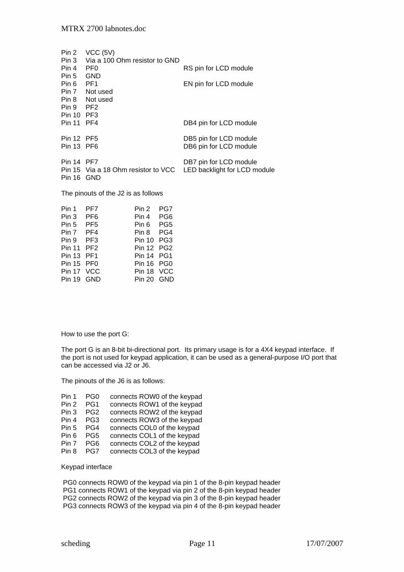
Pin 2 VCC (5V) Pin 3 Via a 100 Ohm resistor to GND Pin 4 PF0 RS pin for LCD module Pin 5 GND Pin 6 PF1 EN pin for LCD module Pin 7 Not used Pin 8 Not used Pin 9 PF2 Pin 10 PF3 Pin 11 PF4 DB4 pin for LCD module Pin 12 PF5 DB5 pin for LCD module Pin 13 PF6 DB6 pin for LCD module Pin 14 PF7 DB7 pin for LCD module Pin 15 Via a 18 Ohm resistor to VCC LED backlight for LCD module Pin 16 GND The pinouts of the J2 is as follows Pin 1 PF7 Pin 2 PG7 Pin 3 PF6 Pin 4 PG6 Pin 5 PF5 Pin 6 PG5 Pin 7 PF4 Pin 8 PG4 Pin 9 PF3 Pin 10 PG3 Pin 11 PF2 Pin 12 PG2 Pin 13 PF1 Pin 14 PG1 Pin 15 PF0 Pin 16 PG0 Pin 17 VCC Pin 18 VCC Pin 19 GND Pin 20 GND How to use the port G: The port G is an 8-bit bi-directional port. Its primary usage is for a 4X4 keypad interface. If the port is not used for keypad application, it can be used as a general-purpose I/O port that can be accessed via J2 or J6. The pinouts of the J6 is as follows: Pin 1 PG0 connects ROW0 of the keypad Pin 2 PG1 connects ROW1 of the keypad Pin 3 PG2 connects ROW2 of the keypad Pin 4 PG3 connects ROW3 of the keypad Pin 5 PG4 connects COL0 of the keypad Pin 6 PG5 connects COL1 of the keypad Pin 7 PG6 connects COL2 of the keypad Pin 8 PG7 connects COL3 of the keypad Keypad interface PG0 connects ROW0 of the keypad via pin 1 of the 8-pin keypad header PG1 connects ROW1 of the keypad via pin 2 of the 8-pin keypad header PG2 connects ROW2 of the keypad via pin 3 of the 8-pin keypad header PG3 connects ROW3 of the keypad via pin 4 of the 8-pin keypad header
scheding Page 11 17/07/2007
MTRX 2700 labnotes.doc
PG4 connects COL0 of the keypad via pin 5 of the 8-pin keypad header PG5 connects COL1 of the keypad via pin 6 of the 8-pin keypad header PG6 connects COL2 of the keypad via pin 7 of the 8-pin keypad header PG7 connects COL3 of the keypad via pin 8 of the 8-pin keypad header The PG0-PG7 has a 100K pull-up resister in each line. The keypad scan routine will set PG3 low, PG0,PG1,PG2 high, and then test the PG4-PG7 If no key is down, PG4-PG7 remain high. If PG7 = low, the key 15 is down. If PG6 = low, the key 14 is down. If PG5 = low, the key 13 is down. If PG4 = low, the key 12 is down. The keypad scan routine then set PG2 low, PG0,PG1,PG3 high then test the PG4-PG7 If no key is down, PG4-PG7 remain high. If PG7 = low, the key 11 is down. If PG6 = low, the key 10 is down. If PG5 = low, the key 9 is down. If PG4 = low, the key 8 is down. The keypad scan routine then set PG1 low, PG0,PG2,PG3 high then test the PG4-PG7 If no key is down, PG4-PG7 remain high. If PG7 = low, the key 7 is down. If PG6 = low, the key 6 is down. If PG5 = low, the key 5 is down. If PG4 = low, the key 4 is down. The keypad scan routine then set PG0 low, PG1,PG2,PG3 high then test the PG4-PG7 If no key is down, PG4-PG7 remain high. If PG7 = low, the key 3 is down. If PG6 = low, the key 2 is down. If PG5 = low, the key 1 is down. If PG4 = low, the key 0 is down. SPI port pinouts are as follows: Pin 1 VCC (5V) Pin 2 VCC (5V) Pin 3 PF2 (LOAD) Pin 4 SPI DATA IN Pin 5 PF3 ( STROBE) Pin 6 SPI DATA OUT from 68HC11 Pin 7 not used Pin 8 PD4 (CLOCK) Pin 9 GND Pin 10 GND All on-board jumpers: J1 40 pin logic analyzer connector, HC11 EVM compatible J2 Port F and Port G, total 16 bits, the left side is port F and the right side is port G J3 LCD port J4 SPI connector J5 Mode selector J6 4 X 4 keypad interface J7 RS485 direction control, hard wired J8 HC11 SCI receiver source selector ( numbering from top to bottom)
1= SCI PD0 receives signal from your target 2= SCI PD0 receives signal from P3, US232 input. 3= SCI PD0 receives signal from the RS485 port, RJ12 jack. 4= SCI PD0 receives signal from on board IR transceiver.
scheding Page 12 17/07/2007
MTRX 2700 labnotes.doc
J9 the PRG/RUN jumper is used for changing between programming mode and run mode.
When it’s in the right position, the board is used for programming the 68HC711E9 chip.
When it’s in the left position, it enables normal debugging session.
J10 Connects the VR1 trimmer pot to the PE7 of the ADC. J11 Analog voltage reference selector
When it’s in the right position, the on-board 5V DC is the reference voltage When it’s in the left position, the user target provides the ADC reference voltage.
J12 Clock selector When it’s in the right position (labeled with ‘INT’), the clock is provided by the on-
board crystal. When it’s in the left position, (labeled with ‘EXT’), the user target provides a HC compatible clock source.
J13 Sensor port. The top line is the signal, the middle line is VCC and the bottom line is GND.
Digital sensors can be connected to the PA0,PA1,PA2 and PA7. The analog sensor can be connected to the PE0 and PE1. There are no pullup resistors on the PE0 and PE1.
J14 Enables speaker. The speaker is driven by the PA5, Output Comparator 3 through the jumper J14.
In some robot applications, the PA5 could be a PWM signal to drive a servo and the jumper J14
should be removed to preserve the PWM signal integrity. J15 The jumper B600 is used for starting program from the EEPROM address $B600. By install this
Jumper the user program can be auto started during power up. When the jumper is installed the LED
below it will be lit to indicate this auto boot mode. User has to place a JMP instruction at the $B600-
$B602 to tell the 68HC11 where to start the user program. In normal debugging session, this jumper
must not be installed, so the LED should de off. J16 Connects the HC11 SCI’s PD1 to all communication hardware (RS232, RS485 and
IR transceiver)on this development board. It is hard wired. J17 IR transceiver control source selector.
When it’s in the up position (labeled with ‘UART’), the HC11’s PD1drives the IR transmitter and
the HC11’s PD0 receives the data from the IR receiver. The PD0 and PD1 can be general I/O lines or the SCI UART. When it’s in the low position (labeled with ‘PA26’), the HC11’s PA6 drives the IR
transmitter and PA2 receives the data from the IR receiver.
J18 Enables the 7 segment LED display driver U11, 74HC367. If the 7 segment LED display is not needed in any application, remove this jumper will turn off the display.
The MODEA and MODEB jumpers are not used in debugging sessions. They are only used for programming the 711E9 OTP part in bootstrap mode. The P3 DB9 female connector is configured as DCE device and it can be directly connected to the PC ‘s com port. BUFFALO I/O routines.
Some universities use the book "MC68HC11 An Introduction Software and Hardware Interface" by Professor Han-Way Huang. The book has several example programs that access BUFFALO I/O routines. The BUFFALO I/O routines located at $FFA0-$FFCF that
scheding Page 13 17/07/2007
MTRX 2700 labnotes.doc
should not be there in the first place. These locations should be reserved by user’s program. We move the BUFFALO I/O locations to $7FA0-$7FCF. Following are the BUFFALO I/O routines’ function description and jumper table: ORG $7FA0 UPCASE convert the character in A to uppercase WCHEK test the character in A for white space and returns with the Z bit set if A is a white space (Space, comma, tab) DCHEK test the character in A for white space and returns with the Z bit set if A is a carriage return or white space (Space, comma, tab) INIT initialize SCI, is not needed with the EP2711E9 board INPUT reads PC keyboard input OUTPUT writes the character in the A to CRT display OUTLHLF converts 4 most Significant Bit of A to ASCII and Writes it to CRT display OUTRHLF converts 4 most Significant Bit of A to ASCII and Writes it to CRT display OUTA output ASCII character in A to CRT display OUT1BYT converts the binary byte that is pointed to by X register to 2 ASCII bytes and write them to CRT display OUT1BSP it’s OUT1BYT followed by sending a space to the CRT display OUT2BSP converts the binary word (2 bytes) that is pointed to by X register to 4 ASCII bytes and write them followed a space to CRT display OUTCRLF write carriage return, line feed to CRT display. OUTSTRG it’s OUTCRLF followed by writing the ASCII string that is pointed to by X register to CRT display and until character is $04 OUTSTRG0 it’s OUTSTRG without writing leading carriage return & line feed to CRT display INCHAR waits for an ASCII character from keyboard and put it in accumulator A Jump Table $7FA0 UPCASE $7FA3 WCHEK $7FA6 DCHEK $7FA9 INIT $7FAC INPUT $7FAF OUTPUT $7FB2 OUTLHLF $7FB5 OUTRHLF $7FB8 OUTA $7FBB OUT1BYT $7FBE OUT1BSP $7FC1 OUT2BSP $7FC4 OUTCRLF $7FC7 OUTSTRG $7FCA OUTSTRG0 $7FCD INCHAR
scheding Page 14 17/07/2007
MTRX 2700 labnotes.doc
We have added several I/O routines in the beginning of our Phantom Monitor. Following are the Phantom Monitor’s I/O routines’ function description and jumper table starting at $7000: ORG $7000 RS485_RECV sets the RS485 port to receiver mode. RS485_XMIT sets the RS485 port to transmitter mode GET_DATE X register points to a 10 byte RAM block before calling this subroutine, it
returns the date information of host PC in the format of MM-DD-YYYY. GET_TIME X register points to an 11 byte RAM block before calling this subroutine,
it returns the time information of host PC in the format of HH:MM:SS AM or HH:MM:SS PM.
OUTSTRG00 It’s OUTSTRG0 except the ending character is $00, instead of $04. LCD_INI initialize the 16x2 LCD LCD_LINE1 displays 16 characters on the first line of a 16X2 LCD display module LCD_LINE2 displays 16 characters on the second line of a 16X2 LCD display module SEL_INST selects instruction before writing LCD module SEL_DATA selects data before writing LCD module WRT_PULSE generates a write pulse LCD module SEVEN_SEGMENT: converts Accu A to segment pattern, bit 7 of the Accu A = Decimal Point of the 4 digit LED display module. Jump Table $7000 RS485_RECV $7003 RS485_XMIT $7006 GET_DATE $7009 GET_TIME $700C OUTSTRG00 $700F LCD_INI $7012 LCD_LINE1 $7015 LCD_LINE2 $7018 SEL_INST $701B SEL_DATA $701E WRT_PULSE $7021 SEVEN_SEGMENT
scheding Page 15 17/07/2007
MTRX 2700 labnotes.doc
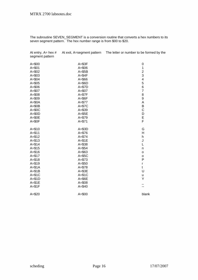
The subroutine SEVEN_SEGMENT is a conversion routine that converts a hex numbers to its seven segment pattern. The hex number range is from $00 to $20. At entry, A= hex # At exit, A=segment pattern The letter or number to be formed by the segment pattern A=$00 A=$3F 0 A=$01 A=$06 1 A=$02 A=$5B 2 A=$03 A=$4F 3 A=$04 A=$66 4 A=$05 A=$6D 5 A=$06 A=$7D 6 A=$07 A=$07 7 A=$08 A=$7F 8 A=$09 A=$6F 9 A=$0A A=$77 A A=$0B A=$7C B A=$0C A=$39 C A=$0D A=$5E D A=$0E A=$79 E A=$0F A=$71 F A=$10 A=$3D G A=$11 A=$76 H A=$12 A=$74 h A=$13 A=$1E J A=$14 A=$38 L A=$15 A=$54 n A=$16 A=$63 o A=$17 A=$5C o A=$18 A=$73 P A=$19 A=$50 r A=$1A A=$78 t A=$1B A=$3E U A=$1C A=$1C u A=$1D A=$6E Y A=$1E A=$08 _ A=$1F A=$40 -- A=$20 A=$00 blank
scheding Page 16 17/07/2007

MTRX 2700 labnotes.doc
INTRODUCTION
The Ep2711E9, a low cost and high performance development board, provides real time emulation for the Motorola 68HC11microcontroller E family. It offers all useful features of the Motorola EVB board with the Buffalo monitor and adds numerous enhancements at an extremely low cost. It combines a complete 68HC11 development system, an advanced trainer, a reliable 711E9 programmer and a versatile SBC into one package. For engineers, it’s a WICE in-circuit emulator development system and Motorola EVB, EVM, EVS replacement, a convenient prototype platform, and a low cost single board computer. For students, it’s a user-friendly microcontroller trainer. It is as powerful as a high priced real-time in-circuit emulator, but it’s affordable as a low cost single board computer.
Ep2711E9 includes user-friendly IDE software which runs under Windows® 95, 98, 2000 and XP. It offers fast file transfer, single-stepping, breakpoints, data watch for memory and registers, symbolic debugging compatibility with most assemblers and compilers, and user program termination with the <Esc> key. Our exclusive phantom monitor™ technology preserves all interrupt vectors including RESET and All on-chip RAM ($00-$1FF), EEPROM, and 30K external emulation RAM ($8800-$FFFF) available for user applications - there is no pre-empted chip memory. The hardware includes a prototype area, 16 extra I/O ports F and G, one logic probe, on board 16X2 LCD display with backlight, 4x4 keypad connector, 8 sensor I/O port, SPI port, speaker, 4-digit LED display, potentiometer, 8 LED status indicators for port B, one 8 position DIP switch connected to port C and three pushbutton switches, dual UART, RS485 interface, IR transceiver with on-board 38 KHz OSC, on-board 12 programming voltage supply and 60-pin EVB/EVBU-compatible connector.
scheding Page 17 17/07/2007
MTRX 2700 labnotes.doc
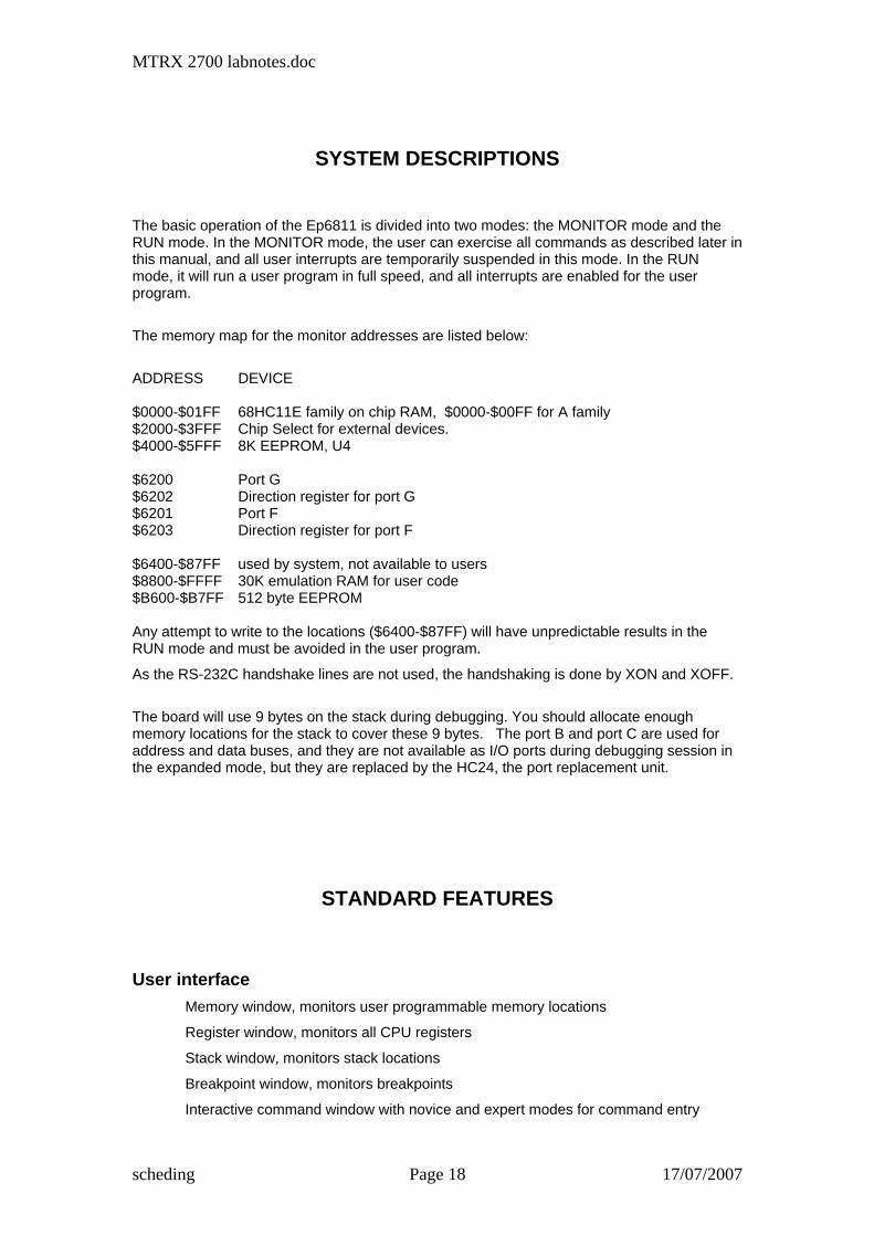
SYSTEM DESCRIPTIONS
The basic operation of the Ep6811 is divided into two modes: the MONITOR mode and the RUN mode. In the MONITOR mode, the user can exercise all commands as described later in this manual, and all user interrupts are temporarily suspended in this mode. In the RUN mode, it will run a user program in full speed, and all interrupts are enabled for the user program.
The memory map for the monitor addresses are listed below:
ADDRESS DEVICE $0000-$01FF 68HC11E family on chip RAM, $0000-$00FF for A family $2000-$3FFF Chip Select for external devices. $4000-$5FFF 8K EEPROM, U4 $6200 Port G $6202 Direction register for port G $6201 Port F $6203 Direction register for port F $6400-$87FF used by system, not available to users $8800-$FFFF 30K emulation RAM for user code $B600-$B7FF 512 byte EEPROM Any attempt to write to the locations ($6400-$87FF) will have unpredictable results in the RUN mode and must be avoided in the user program.
As the RS-232C handshake lines are not used, the handshaking is done by XON and XOFF.
The board will use 9 bytes on the stack during debugging. You should allocate enough memory locations for the stack to cover these 9 bytes. The port B and port C are used for address and data buses, and they are not available as I/O ports during debugging session in the expanded mode, but they are replaced by the HC24, the port replacement unit.
STANDARD FEATURES
User interface
Memory window, monitors user programmable memory locations
Register window, monitors all CPU registers
Stack window, monitors stack locations
Breakpoint window, monitors breakpoints
Interactive command window with novice and expert modes for command entry
scheding Page 18 17/07/2007
MTRX 2700 labnotes.doc
On-line help menu and function key selection
Displays memory in hexadecimal, ASCII, Motorola S-record, Intel Hex or Tektronix Hex formats
Echo debugging session to log file and/or printer
DOS shell facility
Displays internal CPU registers and control bit assignment map using standard Motorola labels
Math function for verifying program results
Memory and register operation
Memory manipulation
Display memory block
Examine and modify memory
Compare memory block
Search memory block for pattern
Move memory block
Fill memory block with pattern
Register manipulation
Examine and modify CPU registers
Breakpoints Set or clear breakpoint address
Assembler and disassembler
Symbolic disassembler and single line symbolic assembler
Automatically disassembles 16 lines of code during assembling
Scrolls display back and forth by page or line during disassembling
Execution Control Execute program
Single step over all instructions, including the RTI instruction
Trace execution File management
File transfer
Download file from host to memory
scheding Page 19 17/07/2007
MTRX 2700 labnotes.doc
Upload memory to host file
Automatically download files during startup
Upload/download of files in Motorola S record,
Intel Hex and Tektronix Hex formats
File formats
Motorola S-record, Intel Hex, Tektronix Hex
Symbol formats
Motorola, 2500AD, Microtek, Zax, Wintek, Introl, Avocet, Archimedes, Whitesmiths, IAR, P&E systems
System Configure INIT, TMSK2, OPTION, BPROT registers
EEPROM erasing and programming
CONFIG register programming in test mode
Scope or logic analyzer trigger output 40 pin logic analyzer connector
scheding Page 20 17/07/2007
MTRX 2700 labnotes.doc
SYMBOLIC DEBUGGER
Predefined names All internal CPU registers can be referenced by their name, such as porta PORTA, portb, PORTB, ddrd, DDRD, etc.
Symbols on the command entry For a command in which an absolute number can be replaced by a symbol, the symbol must start with a ‘\’, such as \BEGIN, \loop. The maximum number of characters in a symbol is 32, and symbol is CASE SENSITIVE. Although symbols can be 32 character long, but the disassembler can only display 10 characters maximum for a symbol. In your source code, it would be better make symbols shorter.
Symbol file format Symbolic debugger reads symbol files which are generated by the Motorola cross assembler ( a public domain program ), the 2500AD, Microtek, Zax assemblers, other popular assemblers and C compilers, including the Wintek, Introl, Avocet, Archimedes, Whitesmiths, and IAR C compilers.
When the Archimedes C compiler is used, you should specify the symbol format by the -Fmpds-m in the xcl file. If you have an assembler or C compiler whose symbol format is not supported by the Ep2711E9 board, we will modify our software to add your symbol format.
COMMAND REFERENCE Command format
The command line format is as follows:
Ep6811->> [Command] [Parameters]
Where: Ep6811->> is the Ep2711E9 prompt. [Command] is the command mnemonic, may be entered in an uppercase or a lowercase
letter. Only the first character of the command is needs to be typed.
[Parameters] are memory addresses or symbols. ALL NUMBERS ARE HEXADECIMAL.
All hex numbers may be substituted by symbols starting with the backslash ‘\’.
Comment:
The fields can be separated by the space or the CR, but a command must be terminated by the CR only.
Errors may be corrected by backspacing or by the ESC key to abort the command. The ESC character will abort the command at any time.
Only a valid key will be accepted on the command line and any invalid keys will NOT be echoed to the CRT display.
scheding Page 21 17/07/2007
MTRX 2700 labnotes.doc
Command reference
The command reference is listed in alphabetical order.
Assemble Syntax:
Assemble [address]
Description:
[address] is the starting address for the assembler operation. Each source line is converted into the proper machine language code and is stored in memory, overwriting previous data on a line-by-line basis at the time of entry.
Caution:
When a new source line is assembled, the assembler overwrites what was previously in the memory. If the assembler detects an error in the new source line, it will output an error message, then re-open the same address location, and the contents of the memory will remain unchanged.
Any attempt to assemble at locations of the monitor will be ignored.
Syntax rules:
1. All numerical values are assumed to be hexadecimal, therefore, no base designators are allowed.
2. Operands must be separated by the space character.
Addressing modes are designated as follows:
1. Immediate addressing is designated by preceding the address with the # sign.
2. Indexed addressing is designated by the “,X”. The comma must be preceded by an offset byte (e.g., LDAA 0,X).
3. Direct and extended addressing are specified by the value of the address operand, a value of less than 256 specifying direct addressing, otherwise the extended addressing is implied.
4. Relative offsets for branch instructions are computed by the assembler. Therefore the valid operand for any branch instructions is the branching address, not the relative offset.
Subcommands:
ASM [address] starts assemble at a new location. FCB [byte]....... allocates a hex byte for each location. FCC [byte]....... allocates an ASCII byte for each location. BYTE [byte]....... as same as FCB DB [byte]....... as same as FCB ASCII [byte]....... as same as FCC
The assembler’s subcommands are available only when an assemble command is executed. For the FCB or FCC subcommand, a maximum of 32 bytes may be entered on a command line.
Example:
scheding Page 22 17/07/2007
MTRX 2700 labnotes.doc
Assemble F000 ; This command starts assemble at the address location $F000.
ldaa #10 ; load Accumulator A with the hex #$10 ldab 2,x ; load Accumulator B with the value of the address that is 2
plus the value of the ; X register
staa 5 ; store the value of the Accumulator A in the direct RAM location 5
staa 1200 ; store the value of the Accumulator A in the extended RAM location $1200
bra f000 ; branch to the location $f000 Breakpoint Syntax:
Breakpoint [address]
Description:
The breakpoint is set at the location specified by the address. The breakpoint can only be set at instruction addresses. A maximum of eight breakpoints may be set.
All breakpoints are software breakpoints.
Comment:
During initial power up all breakpoints are automatically cleared. Example:
Breakpoint F010 This command sets a breakpoint at the address location $F010.
Compare Syntax:
Compare [address1] [address2] [address3]
Description:
[address1] is the starting address of the 1st memory block.
[address2] is the ending address of the 1st memory block.
[address3] is the starting address of the 2nd memory block.
The Compare command allows the user to compare a memory block with another. If the address3 is not specified, the block of memory residing from address1 to address2 will be compared with the block memory residing from address1-1 to address2-1.
Example:
Compare F000 F03F E000
This command compares 64 bytes of the memory block1 from $F000 to $F03F with the memory block2 from $E000 to $E03F.
Dump Syntax:
scheding Page 23 17/07/2007
MTRX 2700 labnotes.doc
Dump [address1] [address2] Description:
[address1] is the starting display address. It defaults to the address which equals the ending address from the last memory dump plus 1.
[address2] is the ending display address. It defaults to the address which equals the address1 plus
3F(in hex).
The Dump command allows the user to display a block of memory beginning at the address1 and continuing to the address2. If the address2 is not entered before the Carriage Return is entered, 64 bytes of memory are displayed beginning at the address1.
Example:
Dump F000 F0FF
This command displays a block of memory beginning at $F000 and continuing to $F0FF.
Enter Syntax:
Enter [address]
Description:
[address] is the memory location at which to start examining and/or modifying.
The Enter command allows the user to examine and/or modify contents in memory at specified locations in an interactive manner. Once entered, the enter command has several subcommands that allow modification and verification of the memory contents.
Following are the subcommands that are recognized by this command:
<Enter> ; examine/modify the next location. <-> ; examine/modify the previous location. <ESC> ; exit from the Enter mode.
Caution:
Any attempt to modify at address locations of the monitor will be ignored.
Example:
Enter F000
F000 00/ ; display data at the address $F000. F000 00/AA ; change data at $F000 from 00 to AA. F001 11/ ; display data at the next address $F001.
Fill Syntax:
Fill [address1] [address2] [pattern]
Description:
scheding Page 24 17/07/2007
MTRX 2700 labnotes.doc
[address1] is the lower limit of the memory block. It defaults to the address which equals the ending address from the last DUMP command plus 1.
[address2] is the upper limit of the memory block. It defaults to the address which equals the address1 plus 3F (in hex).
[pattern] is the data pattern in hexadecimal values. It defaults to 00 by entering the space character.
The Fill command allows the user to repeat a specific pattern (up to 16 bytes) throughout a determined memory range. The data bytes must be separated by the space character. The Carriage Return will end this command.
Caution:
Any attempt to fill address locations of the monitor will be ignored.
Example:
Fill F000 FFFF 00
This command fills locations $F000 through $FFFF with 00’s.
Go Syntax:
Go [address]
Description:
[address] is the starting address where the program execution begins. The G command allows the user to initiate the program execution (free run in real-time). The user may optionally specify a starting address where execution is to begin. The program execution starts at the current program counter address location, unless a starting address is specified. The program execution continues until a breakpoint is encountered, or the ESC key, or the reset switch is depressed.
Example:
Go F000
This command starts execution at the address location $F000.
Init Syntax:
Init [value1] [value2] [value3] [value4]
Description:
[value1] is the new value for the INIT register. [value2] is the new value for the TMSK2 register. [value3] is the new value for the OPTION register. [value4] is the new value for the BPROT register.
The user will be prompted to enter all 4 values, press the CR to skip the modification or the ESC key to cancel the modification. The INIT register, the BPROT register, the
scheding Page 25 17/07/2007
MTRX 2700 labnotes.doc
bit 0,1,4,5 of the OPTION register, and the bit 0,1 of the TMSK2 register can be modified only within first 64 E cycles after a system reset.
The Init command will automatically generate a reset signal on the 68HC11 in order to force the 68HC11 to take new values for these 4 control registers.
Caution:
Any other commands, such as Enter, Fill or Move, will not reset the 68HC11, and will not have any effect on the INIT register, the BPROT register, the bit 0,1 of the TMSK2 register and bit 0,1,4,5 of the OPTION register.
Before executing a user program the value of the above four registers must be set correctly. If a user program modifies these registers in its initialization routine, the user must use the I command to modify these registers with the same values.
Kill breakpoint Syntax:
Kill breakpoint [address]
Description:
The breakpoint is cleared at the location specified by the address. If the address is not specified, all breakpoints will be cleared.
Example:
Kill breakpoint F010
This command clears the breakpoint address location $F010.
Load Syntax:
Load [filename] [offset]
Description:
The Load command will prompt the user to enter the type of the file to be downloaded. This command can download the user file, or the symbol file, or the system parameter file. The parameter file includes the EEPROM programming enable/disable flag, the INIT, TMSK2,OPTION and BPROT registers, the breakpoint addresses, the memory display addresses
If the type of the file is a user file which is in the Motorola S record, or the Intel hex, or the Tektronix Hex format. The user will be prompted with the following parameters:
[filename] is the filename to be download from the host PC. [offset] is the offset to be added with the download addresses.
If the type of the file is the symbol file or the parameter file the user would be prompted to enter file name. The Load command downloads user files in the Motorola S record, or Intel hex or Tektronix hex format from the PC into the Ep2711E9 board. Before download of the user file, the user will be prompted to input an offset value which will be added to the download addresses of a host file to generate the absolute addresses for the Ep2711E9 board. If the offset is not needed, just press the Carriage Return. By using this offset feature, a file can be downloaded into different memory blocks.
scheding Page 26 17/07/2007
MTRX 2700 labnotes.doc
Caution:
Always download the symbol file first, so the symbols in a parameter file will have
their values. Any attempt to download data from a file into the address locations of the monitor will
be ignored.
Example:
Load test.s19 8000
This load command downloads the file named test.s19 from the host PC into the Ep2711E9 board. It will add $8000 with all memory addresses of the file. For instance, the data at the address $1000 of the file will be downloaded into the location $9000 instead of $1000, because every download address is added with $8000.
Move Syntax:
Move [address1] [address2] [address3]
Description:
[address1] is the starting address of source memory block. [address2] is the ending address of source memory block. [address3] is the starting address of destination memory block.
The Move command moves the contents of the source memory block to the destination memory block. If the destination memory block is not specified, all data residing from the address1 to the address2 will be moved up one location.
Caution:
Any attempt to move data to the address locations of the monitor will be ignored.
Example:
Move F000 F03F E000
This move command moves 64 bytes of data at the memory block between $F000 and $F03F to the memory block between $E000 and $E03F.
Next step (single-step) Syntax:
Next step
Description:
The N command allows the user to monitor program execution on an instruction-by-instruction basis. It will execute one instruction (including the RTI instruction) whose location is pointed to by the program counter. After a single-step, the PC will display all CPU register values and the next instruction to be executed.
scheding Page 27 17/07/2007
MTRX 2700 labnotes.doc
Program memory watch Syntax:
Program
Description:
The P command allows the user to select 3 blocks of 2 contiguous memory locations and 3 blocks of 8 contiguous memory locations for memory watching purpose. These locations will always be updated after using the Assemble, Enter, Fill, Move, Go, or Next Step commands.
All six starting addresses can be substituted by symbols. For example, \DATA is 0005 if the value of the symbol \DATA is 0005, \message is E100 if the value of the symbol \message is E100.
Register modify Syntax:
Register modify
Description:
The R command allows the user to display and modify: PC - program counter, CC - condition code register, B - Accumulator B, A - Accumulator A, X - Index register X, Y - Index register Y, SP - stack pointer. After modifying the value of a register, press the CR to complete modification and press the ESC key to exit from the command.
Caution:
The stack pointer should be modified with a great care. It should only be modified when nothing was pushed onto the stack, otherwise the return address and flag register that were pushed onto the old stack must be manually moved to the new stack area to prevent a crash.
Search Syntax:
Search [address1] [address2] [hex data pattern]
Description:
[address1] is the starting address of the memory block to be searched.
[address2] is the ending address of the memory block to be searched. It defaults at the address which equals the address1 plus 3F(in hex).
[pattern] is the data pattern to be searched for.
The Search command allows the user to search for a specific pattern (up to 16 bytes) throughout a specified memory range. The data bytes must be separated by the space character. The Carriage Return will end this command.
scheding Page 28 17/07/2007
MTRX 2700 labnotes.doc
Example:
Search F000 FFFF 01 02 03 04 05 06 07 08
This command will search for the pattern of 8 hex numbers,which are 01 02 03 04 05 06 07 08, in the memory range between $F000 and $FFFF.
Trace Syntax:
Trace [number of steps]
Description:
The Trace command allows the user to trace program execution for a specified number of steps on an instruction-by-instruction basis. During the trace, the PC will display all register values and the next instruction to be executed after each step.
Unassemble Syntax:
Unassemble [address]
Description:
[address] is the starting address for the disassembler operation. If no address is specified, the starting address is the one that followed the last instruction unassembled by the previous U command.
The U command will disassemble 16 lines of instructions. All valid opcodes are converted to the assembly language mnemonics, and all invalid opcodes are replaced by the FCB’s. The PgUp, PgDn , , Home keys can be used to scroll display back and forth.
Write Syntax:
Write [filename] [address1] [address2] [M/I/T]
Description:
The Write command will prompt the user to enter the type of the file to be saved. This command can upload the user file, or the symbol file, or the system parameter file. The parameter file includes the EEPROM programming enable/disable flag, the INIT, TMSK2, OPTION and BPROT registers, the breakpoint addresses, and the memory display addresses.
If the type of the file is the user file which is in the Motorola S record, or the Intel hex, or the Tektronix Hex format. The user will be prompted with the following parameters:
[filename] is the filename to be saved in the host PC.
[address1] is the starting address of the memory block to be saved.
[address2] is the ending address of the memory block to be saved.
scheding Page 29 17/07/2007
MTRX 2700 labnotes.doc
[M/I/T] is the file format in which the user file is saved. Enter M for the Motorola S record, I for the Intel Hex format or T for the Tektronix Hex format.
If the type of the file is the symbol file or the parameter file, the user would be prompted to enter the file name only
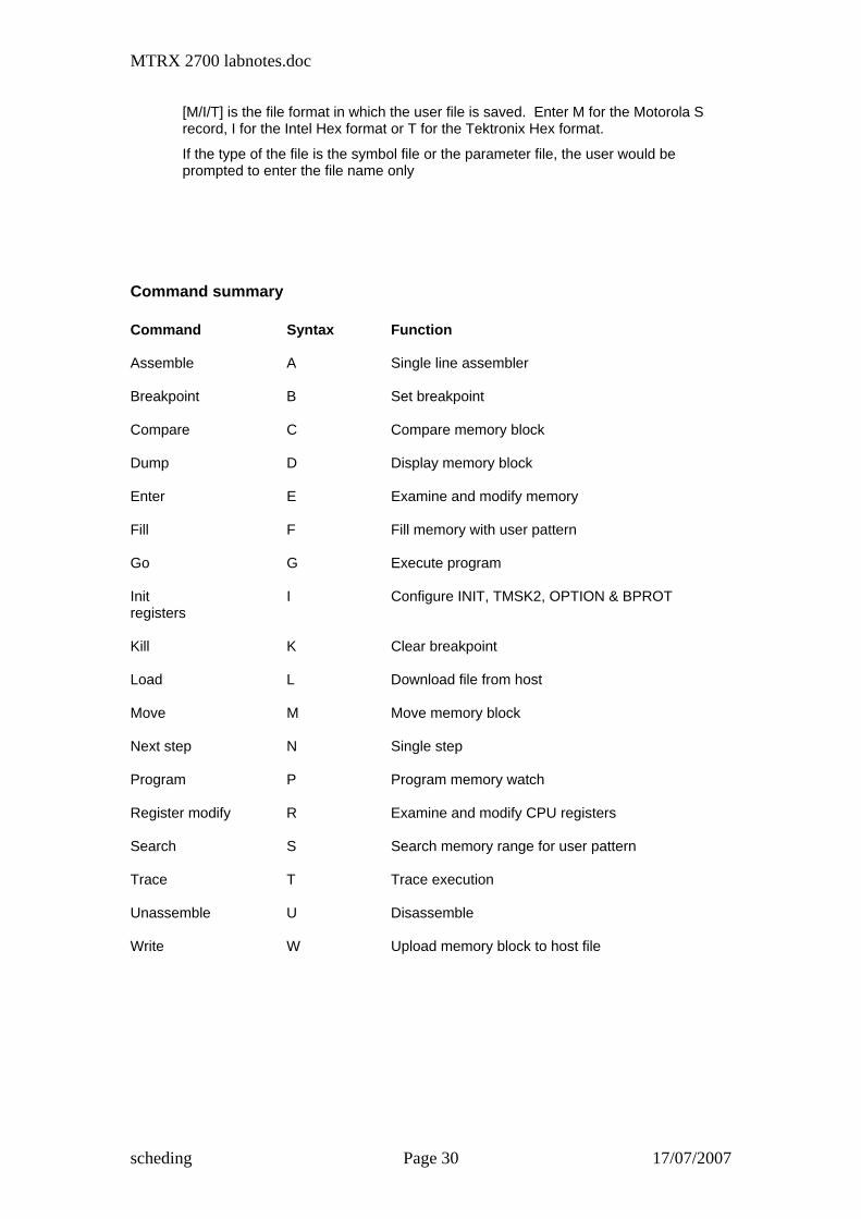
Command summary Command Syntax Function Assemble A Single line assembler Breakpoint B Set breakpoint Compare C Compare memory block Dump D Display memory block Enter E Examine and modify memory Fill F Fill memory with user pattern Go G Execute program Init I Configure INIT, TMSK2, OPTION & BPROT registers Kill K Clear breakpoint Load L Download file from host Move M Move memory block Next step N Single step Program P Program memory watch Register modify R Examine and modify CPU registers Search S Search memory range for user pattern Trace T Trace execution Unassemble U Disassemble Write W Upload memory block to host file
scheding Page 30 17/07/2007
MTRX 2700 labnotes.doc
FUNCTION KEY ASSIGNMENT F1: A brief on-line help.
F2: Emulation memory map.
F3: Not used.
F4: Dump memory contents in the Motorola S record, or the Intel Hex format or the Tektronix Hex format.
F5: This key allows the user to echo CRT output to printer and/or log file on the disk.
F6: This key displays all 68HC11 control registers and control bit assignments.
F7: This function evaluates a numerical operand, or performs arithmetic and logical operations on a simple expression, giving the result in Hex, Decimal, Octal, Binary, valid ASCII character, one's complement and valid negative number. The arithmetic operations are addition (+), subtraction (-), multiplication (*), and division (/). The logical operations are AND (&), OR (|), Exclusive OR (^), left shift (<) and right shift (>). The default notation is HEX, a decimal, octal, or binary number must be followed by the letter T, O, and Q. The result in the first line is HEX, Decimal, Octal, Binary and ASCII character if the value of the result is between 0x20 to 0x7F. The result in the second line is one’s complement, negative number if the value of the result is between 0x80 to 0xFF in 8 bit format, 0x8000 to 0xFFFF in 16 bit format, and 0x80000000 to 0xFFFFFFFF in 32 bit format.
F8: This key allows the user to erase or program the EEPROM of the 68HC11.
F9: This key allows the user to display and edit the symbol table. Use the Load command to read symbol files which are generated by the Motorola cross assembler (a public domain), 2500 AD, Microtek, Zax assemblers, Wintek, Introl, Avocet, Archimedes, Whitesmiths, IAR C compilers or Wytec format directly. No conversion is needed.
F10: This key allows the user to do:
1. Terminate the emulation and exit from the debugger, or
2. Re-start the emulation without terminating. It is often called warm boot and is useful to initialize the CRT screen. For instance, when the PC reads a file from a floppy disk drive for downloading into the Ep2711E9 board, the PC will print out an error message that will garble the monitor screen, if the door of the drive is left open. This key will restore the screen. It also can be used to automatically download files.
scheding Page 31 17/07/2007
MTRX 2700 labnotes.doc
ALT+F1:
This key combination toggles between the novice and the expert modes. In the novice mode the user will be prompted to enter each parameter on the command line.
QUESTIONS & ANSWERS This chapter contains the most commonly asked questions about the Ep2711E9 board. They are divided into three sections.
1. Hardware 2. Miscellaneous questions
Hardware Q. When I turn on the Ep2711E9 board, how come the LED does not flash? A. After the initial power up, the RESET LED should blink 4 times, otherwise check the
VCC. It should have a reading of about 5V DC. If 5V DC is not present, check if the polarity of DC output of the AC adapter is correct. The center is positive on the DC plug.
check if a jumper is installed on the 'B600' header. If it is, remove it. The 'B600'
jumper is for 68HC11E1 to start code from the on-chip EEPROM. If you program the first 3 bytes of the EEPROM with a JMP instruction, you can auto start the board during power-up, but You must remove the B600 jumper for debugging your code.
The board is running in expanded mode, even it's emulating the 711E9 OTP part.
You must also remove the MODEA and MODEB jumpers for the expanded mode if they were installed for the bootstrap mode, such as programming the 711E9 chip.
If the problem still exists, try starting it up in the test mode by pressing and holding
the PA0 data switch down while resetting the board. If the RESET LED does not flash, then the E1 chip is bad and you have to replace it. If the RESET LED flashes, the chip is good and most likely the COP function is enabled. It will work after re-programming the CONFIG register in the test mode to disable the COP function.
If you have a watchdog circuit with the reset signal, you should disable it during
debugging, only test your watchdog function after your code is completely debugged, otherwise the LED may not flash.
Finally check the EPROM U2 DIP socket for any loose contact. Q. The RESET LED flashes during power up or whenever the reset switch is depressed
but why does the Ep2711E9 board not communicate with the host PC? A. If the LED blinks and there is no response from the Ep2711E9 board, check the RS-
232C cable connection and if the COM port number is configured correctly. Also make sure that you only open the debug window once. If the first debugger is running, you cannot invoke second debugger before closing the first one.
Q. My program works with another SBC but why does it not work when I use the
Ep2711E9? A. The values of the INIT register (shown on the top of the screen) and the TMSK2,
OPTION, and BPROT registers must be set correctly by the Init command before running your program. Because these registers can only be modified in normal modes within the first 64 E cycles, any modification to these registers in the beginning of your program will not change their values when your target program is executed by
scheding Page 32 17/07/2007
MTRX 2700 labnotes.doc
the GO command, because the 64 E cycles period was already passed. The Init command allows you to modify these registers to the correct values before running your target program, because the I command will automatically reset the 68HC11E1, so the modification can be done.
If you don't relocate the control register, the value of the INIT register should be 01.
Always watch this value on the top of the screen. If this value is corrupted by running a bad program, you have to re-program it to 01, or power cycle the board. During the power up, its value is always = 01.
Q. My program works with the Ep2711E9 board but it does not work in another SBC,
why? A. The stack point in your program may not be set in the beginning of your program. The
Ep2711E9 sets the stack point during power up, you should do the same thing in your program. If your resident 68HC11 microcontroller on the Ep2711E9 board is a 68HC11E1, but the 68HC11 on your target is a 68HC11A1, you should be careful to use the PA3 of the PORTA, it is an output line in the A1 controller but a bi-directional line in the E1 controller. You have to program the bit 3 of the PACTL register if you want the PA3 to be an output line. It defaults as an input line during power up.
Q. After executing the program by the GO command why can't the ESC key stop the
Ep2711E9 board? A. In most cases the ESC key can stop the user program, if this is not the case, there
could be many reasons for this problem. Since you cannot use the ESC key to stop the 68HC11, the only thing you can do is to reset the Ep2711E9 board by depressing and releasing the reset button. The reset button of the Ep2711E9 board should be pressed whenever the Ep2711E9 board does not seem to work properly, such as a system crash after running a bad program. Once it is pressed, it will reset the program counter to the reset vector fetched from locations $FFFE and $FFFF, the stack pointer to $00FF, and update the INIT register.
Check if the jumper on the PRG/RUN header is on the RUN position. If the jumper is
set at the PRG position, then you cannot stop program and also the single step function will not work.
Carefully check the user program to determine if there is any attempt to write data
into the memory locations at $6800-$x8FFF. These locations are used by monitor firmware. Any memory write to these locations must be avoided in the user program. In your program, you can disable interrupt temporarily by the SEI instruction, but cannot disable for a long time, because the ESC is relying on interrupt to stop the user program.
Q. I want to modify the CONFIG register, how do I enter the test mode? A. The CONFIG register can only be modified in the test mode. In order to enter the test
mode, press and hold the PA0 switch, then press and release the RESET button and it will start the test mode. By checking the status line on the top of the screen you can tell if you are in the test mode. The Ep2711E9 board cannot emulate the user program in the test mode and the test mode is only used for modifying some registers (such as the CONFIG register) that cannot be modified in both single chip mode and expanded mode.
The status line on the top of the screen indicates the operating mode. The 'EXP' stands for the expanded mode and the 'TST' stands for the test mode. The status line also displays the value of the INIT register, which indicates the locations of the on-chip direct RAM and the 64 control registers.
In the test mode, press the F8 key and follow the instructions to modify the CONFIG register.
Q. Can I modify the CONFIG register in my program after a system reset?
scheding Page 33 17/07/2007

MTRX 2700 labnotes.doc
A. The CONFIG register can only be modified in the test mode. This is a safety feature of the 68HC11. Your program cannot modify it unless your target hardware is set for the test mode.
Miscellaneous questions
Q. What is the parameter file, and how do I create this file?
A. The parameter file includes the EEPROM programming enable/disable flag, the INIT, TMSK2, OPTION and BPROT registers, the breakpoint addresses, the memory display addresses. These parameters can be saved for a particular user program, they should be loaded before running the user program so the program will be executed in a consistent manner. You do not have to make this file by yourself. You can use the W command to save all parameters into a parameter file.
Q. Why does the disassembler display wrong symbols for some instructions, especially
the instructions with 8 bit values?
A. Many cross assemblers do not have any attribute bytes for their symbols. When too many symbols have the same value, the disassembler cannot display the correct symbol for that value. The disassembler will display first two labels it found. Occasionally, when too many symbols have the same value, the disassembler may display a wrong symbol for the value.
Q. I am using the Motorola cross assembler AS11.EXE (a public domain program ), could you show me how to generate a symbol file?
A. Following is the procedure to generate a symbol file from the Motorola cross assembler AS11.EXE (a public domain program) that can be downloaded into the Ep2711E9 board 68HC11 for symbolic debugging. If you are using a different cross assembler, please ignore it.
In windows IDE, just click the make button. If your code has no errors, it will generate s19 file, symbol file and listing file. If your code has errors, it will generate an error listing on the screen with line numbers before the errors.
PFE and MiniIDE
How to install Programmer’s File Editor If you are not satisfied with the EDIT.com program that comes with the board, you can install the Programmer’s File Editor. But you should spend some time to familiarize with the Ep2IDE software before installing the Programmer’s File Editor.
Programmer’s File Editor is one of the best freeware editors for Windows 95, 98, 2000 from Alan Phillips. It also allows you to edit more than one file within the editor. If you have other editor that you like, you can install it to replace the EDIT.com
In order to use the PFE with the EVBplus2 board, you must do:
1. Download the PFE version 1.01 (32 bit version) software from www.download.com, enter PFE to search the PFE101.ZIP file.
2. Unzip it in the drive C, when you are asked to extract to a directory, make it the directory C:\Ep2IDE\PFE
scheding Page 34 17/07/2007
MTRX 2700 labnotes.doc
3. Un-remark (by deleting the rem) the first two lines of text in the beginning of the file EDIT6811.BAT in the directory C:\Ep2IDE
Line1: rem \Ep2IDE\PFE\PFE32 becomes \Ep2IDE\PFE\PFE32
Line2: rem goto end becomes goto end
To modify the edit6811.bat, right click on the start button, left click on the explorer to bring up the explorer, left click on the folder C:\Ep2IDE, right click on the edit6811.bat, a pull down manual appears, left click the edit command to edit the first two lines of the edit6811.bat as shown above. After modifying the edit6811.bat, make sure to save it.
After above installation, you can click the EDIT button to launch the PFE.
You only need to use the FILE commands from the PFE for your 68HC11 development work. Use the FILE command to edit your source code and click the MAKE button to assemble your source code. If the assembler generates an error, it also will show the error’s line number in the file along with the error message. Use the CTRL G to go to the line to make a correction. File download, programming EEPROM should be done in our user-friendly debugger and programming the on-chip EPROM should be done with the PRGM button of the Ep2IDE.
When using the PFE with the EVBplus2 debugger, make sure that the default directory on the PFE must be the same directory that is configured by the debugger as the working directory. The file name to be edited must be the file name that is configured by the debugger.
How to install MiniIDE For some MiniIDE fans, you can install the MiniIDE for your development work, but you should spend some time to familiarize with the Ep2IDE software before installing the MiniIDE.
MiniIDE is an Integrated Development Environment from MGTEK.com
It incorporates an editor, a terminal window and an integrated cross assembler for the 68HC11and HC12.
In order to use this IDE with the EVBplus2 board, you must do:
a. Download the MiniIDE software from www.mgtek.com
b. Install it in the drive C, when you are asked to install it in the default directory c:\Program Files, change it to the directory C:\Ep2IDE\MiniIDE.
c. Un-remark (by deleting the rem) the first two lines of text in the beginning of the file ASM68.11.BAT in the directory C:\Ep2IDE
Line1: rem \Ep2IDE\MiniIDE\MiniIDE becomes \Ep2IDE\MIniLDE\MiniIDE
Line2: rem goto end becomes goto end
To modify the asm6811.bat, right click on the start button, left click on the explorer to bring up the explorer, left click on the folder C:\Ep2IDE, right click on the asm6811.bat, a pull down manual appears, left click the edit command to edit the first two lines of the asm6811.bat as shown above. After modifying the asm6811.bat, make sure to save the file asm6811.bat.
After above installation, you can click the MAKE button to launch the MIniIDE.
You only need to use two commands from the MiniIDE for your 68HC11 development work. Do not use the TERMINAL command. Use the FILE command to edit your source code and the BUILD command to assemble your source code. If the assembler generates an error, it also will show the error’s line number in the file along with the error message. Use the CTRL G to go to the line to make a correction. File download, programming EEPROM should be done in our user-friendly debugger and programming the on-chip EPROM should be done with the PRGM button of the Ep2IDE.
scheding Page 35 17/07/2007
MTRX 2700 labnotes.doc
When using the MiniIDE with the EVBplus2 debugger, make sure that the default directory on the MiniIDE must be the same directory that is configured by the debugger as the working directory. The file name to be edited must be the file name that is configured by the debugger.
If you like the MiniIDE after using for 30 days, you should register with them and send them your contribution to show your appreciation and support.
If you have any technical questions regarding the MiniIDE or you want to make a suggestion or a bug report,
please feel free to email Marius Greuel at [email protected].
If you prefer to use your own DOS based editor, you can do:
I. Modify the file c:\Ep2IDE\ myedit.bat. Basically you add the path of your editor into the path command on the first line of the file myedit.bat.
II. Add two more lines in the beginning of the file edit6811.bat. The first line is “your editor’s name followed by a space character and followed by %1”. The second line is “goto end”. When you click the EDIT button, the IDE will pass the filename to edit6811.bat as the 1st argument on the command line.
If you prefer to use your own DOS based assembler, you can do:
I. Modify the file c:\Ep2IDE\ mymake.bat. Basically you add the path of your assembler into the path command on the first line of the file mymake.bat.
II. Add two more lines in the beginning of the file asm6811.bat. The first line is “your assembler’s name followed by a space character and followed by %1”. The second line is “goto end”. When you click the MAKE button, the IDE will pass the filename to asm6811.bat as the 1st argument on the command line.
scheding Page 36 17/07/2007
File: Mechatronics Laboratory - Introduction.doc Created: DCR, 08/08/2002 13:06:00 Saved: 14/03/2005 08:44:00 Printed: 14/03/2005 08:44:00
School of Aerospace, Mechanical and Mechatronic Engineering
Mechatronics Laboratory
Introductory Notes The Mechatronics Lab is Room 325 in the Link Building. It is a special purpose computer Lab that is provided for mechatronics students, and can generally be used Monday to Friday during normal business hours. We are offering you the privilege of working in the Lab with minimal supervision. In return, you must agree to take all steps necessary to safeguard the lab and its facilities, and to maintain safe and pleasant working conditions. To begin with, we ask that you read these notes thoroughly, and the follow the rules set down here.
1 Use of the Mechatronics Lab • The Mechatronics Lab is generally available (an “open Lab”) for use between the hours of
7:00 am and 6:00 pm, Monday to Friday, unless it is booked for a class. Class bookings will be posted on the Lab door.
• Authorized Lab Users include: any student enrolled in the courses MTRX 1702, MRTX 2700, MRTX 3700, MRTX 4700, or MECH 4730 in the current semester, or (with the approval of mechatronics staff) undertaking thesis work in MECH 4101/2, plus the Tutor(s) and Academic Staff associated with these courses.
• Users are allowed to use the Lab facilities for work in the designated courses only, not for personal use or for other courses. This is a special-purpose lab supporting specific microprocessor and computer engineering courses.
• Physical access to the Lab is restricted by an electronic swipe card. Outside of scheduled class hours, you can ask the subject Tutor(s) or Lecturer(s) to let you into the Lab. Either of the Mechanical Building Attendants (Room S142) can also let also you into the Lab.
2 Rules, Rights and Responsibilities of Users All Lab Users have certain rights and responsibilities, and must agree to follow the rules set out here.
• For safety reasons there must always be at least two people in the Lab. See the section on Lab Safety later in these notes.
• You are not permitted to eat or drink in the lab, due to the increased risk of electrocution, equipment damage, and because of the mess it makes. Take a break – go sit on the lawn, relax and smell the sunshine…
• Respect the test equipment, and be gentle with it. If you don’t know something about a circuit or electronics hardware, ask before rushing ahead. Most of the equipment is quite expensive, and (perhaps more importantly) is impossible to replace at short notice.
• You must not open the PC cases or install additional hardware or software on the Lab computers. If you think that there is a need, please speak to one of the Tutors or Lecturers.
• It is your responsibility to keep the Lab neat and tidy. Electronic prototyping and computer work tend to generate big messes. When you are finished your session, tidy things up for the next person who will use your Lab Workstation. Put unwanted papers in the paper recycling
2 of 6
bag, throw out small scraps of wire, replace manuals in the shelves, etc. All benches should be clear of everything except keyboards and mice. You should aim to leave the Lab neater than you found it.
• Please report any problem, including damage to equipment, as soon as it occurs. Problems may involve the network, Lab server, computer workstation, specialized lab equipment, application software, operating system, usage, etc. It is important that we have as many details as possible so that the problem can quickly be fixed. To report a problem o Send a report by email to [email protected] so that we have written
information on the problem. Make sure that you identify which circuit board, computer, network port, etc. has the fault, and provide as much detail as you can;
o Speak to a course Lecturer or Tutor if one is in the Lab. If the problem is urgent, seek out and speak to a Lecturer or Tutor;
o If the problem involves the possibility of injury to people or damage to equipment, isolate equipment involved from energy sources (e.g. 240V AC) and tag it with a warning label. Warning labels are stored in the small box near the right side of the whiteboard. Please put your name and the date on any tags that you write.
• The last person out must secure the Lab, as follows: o Turn off all PC monitors and instruments – the PCs should remain powered; o Close the windows; o Turn off the ceiling fans; o Turn off all lights; o Put out the cat; o Make sure that the door is locked behind you; o Check the door again.
User behaviour will be monitored by course Tutors/Lecturers. Sanctions may be imposed upon people who breach the rules, including exclusion from the Lab for a number of weeks, or referral to the Registrar for further disciplinary action.
3 Lab Safety1 It is said2 that the “accident rate in schools and colleges is 100 to 1000 times greater than [in industry]”. As you learn about engineering and scientific principles it is also important that you learn about safety. To work safely in the Lab means that
• You know the hazards; • You know the likely and worst incidents that could happen; • You know what to do and how to do it if they should happen; • You know and use practices and protective equipment to eliminate or control the risks.
The main hazards in the Lab are
• Electrical hazards; • Danger of slips, trips and falls.
The probability of either of these happening is assessed as small, provided that safe practices are observed. This section describes some of these practices.
1 Some of this material is abstracted (with permission) from a document prepared by Michigan State University. 2 http://www.labsafety.org/

3 of 6
3.1 Electrical Hazards The severity and effects of an electrical shock depend on a number of factors, such as the pathway through the body, the amount of current, the length of time of the exposure, and whether the skin is wet or dry. Water is a great conductor of electricity, allowing current to flow more easily in wet conditions and through wet skin. The effect of the shock may range from a slight tingle to severe muscular contraction, to severe burns to cardiac arrest, depending on the voltage, current and the duration of the shock. Table 1 shows the general relationship between the degree of injury and amount of current for an 110V AC hand-to-foot current path of one second’s duration of shock. While reading this chart, keep in mind that normal 240V AC electrical circuits can provide continuously up to 10 A of current flow. Even voltages as low as 40V can be dangerous.
Table 1: Response of the human body to current – 110VAC for 1 second.
Current Reaction 1 mA Perception level 5 mA Slight shock felt; not painful but disturbing
6 – 30 mA Painful shock; "let-go" range 50 – 150 mA Extreme pain, respiratory arrest, severe muscular contraction
1,000 – 4,300 mA Ventricular fibrillation ≥ 10,000 mA Cardiac arrest, severe burns and probable death
The major hazards associated with electricity are electrical shock and fire. Electrical shock occurs when the body becomes part of an electric circuit, either when an individual comes in contact with both wires of an electrical circuit, one wire of an energized circuit and the ground, or a metallic part that has become energized by contact with an electrical conductor.
3.1.1 Electrical Hazard Reduction There are various ways of protecting people from the hazards caused by electricity, including insulation, guarding, grounding, and electrical protective devices such as fuses and residual current devices3 (RCDs). This section provides a set of simple rules aimed at reducing electrical hazards within the Mechatronics Lab. Most of the hazards relate to 240V AC mains-powered equipment.
Electrical hazards can be reduced significantly by taking some basic precautions:
• Know the location of, and how to operate, the emergency electrical power isolator – it is the red Emergency Stop button which is located on the wall next to the internal office window. Use this button to instantly shut off all electrical equipment in the Lab in the event of electrocution or fire.
• Visually inspect wiring of mains-powered equipment for defects such as faulty insulation or loose connections before each use. Do not use damaged or frayed electrical cords. Tag and report them as unsafe immediately.
• Remove metal jewellery, watches, rings, etc., before working on electrical circuits.
3 Formerly known as earth leakage circuit breakers (ELCBs)
DANGER! Students are not permitted to work on circuits that are energised by 240V AC or 415V AC power under any circumstance. The phrase “work on” shall include activities such as opening the cabinet of a mains-powered instrument, and measuring mains-powered circuits with test instruments.

4 of 6
• Minimize the potential for liquid spills on or near electrical equipment. Never place containers of liquid, including beverages, on or near electrical systems.
• Always know the electrical ratings of equipment you use, and be sure you use that equipment within its ratings. Never overload circuits.
• Turn off power and unplug equipment before checking or replacing fuses. Locate and correct the cause of a blown fuse or tripped circuit breaker before replacing the fuse or resetting the circuit breaker.
• Never defeat the purpose of a fuse or circuit breaker. Never install a fuse of higher amperage rating than that specifically listed for the circuit.
• Complete all your wiring and check it carefully before turning on the power supply. If you are at all uncertain, have it checked by someone else – preferably a Lecturer or Tutor.
• When a setup or circuit is to be reconfigured or rewired, turn the power supply off. It is also good practice to disconnect it physically from the power supply.
• Make sure metallic equipment chassis or cabinets are earthed. Never cut off or defeat the protective earth connection on a plug.
3.1.2 Electrical Emergency Response The following instructions provide guidelines for handling three types of electrical emergencies.
3.1.2.1 Emergency Electrical Power Isolator
3.1.2.2 Electric Shock
If someone suffers serious electrical shock, he or she may be knocked unconscious. If the victim is still in contact with the electrical current, immediately disconnect the electrical power source using the red Emergency Stop button which is located on the wall next to the internal office window. If the supply does not disconnect, try to separate the victim from the power source with a nonconductive object, such as a wooden-handled broom.
Important: Do not touch an electric shock victim who is still in contact with a power source; you could electrocute yourself.
Have someone phone for emergency medical assistance immediately (0-000 from an internal phone or 112 from a GSM mobile phone). Administer appropriate first-aid. Notify the University Emergency Service by internal phone on 1-3333, or 9351-3333 from a mobile phone.
3.1.2.3 Electrical Fire
If an electrical fire occurs, immediately disconnect the electrical power source using the red Emergency Stop button which is located on the wall next to the internal office window, but only if you can do it without endangering yourself. If the fire is small, you are not in immediate danger, and you have been trained in fighting fires, use any type of fire extinguisher except water to extinguish the fire.
Important: Do not use water on an electrical fire.
If the fire is not controlled, activate the Break Glass Alarm which is located just inside the Lab entry door. Both the Fire Brigade and the University Emergency Service will respond immediately.
In the case of an electrical emergency, such as electrocution or fire, all 240V and 415V general purpose power outlets in the lab can be isolated (turned off) by pushing the red Emergency Stop button which is located on the wall next to the internal office window.
5 of 6
3.1.2.4 Live Conductors, Including Power Lines
Stay away from live conductors and downed power lines. Be particularly careful if a live conductor is touching a body of water. The water could conduct electricity. If a power line falls on your car4 while you are inside, remain in the vehicle until help arrives.
3.1.3 Slips, Trips and Falls Injuries in the workplace are most likely to be caused by very common hazards – the ones that no one thinks about. The danger of slips, trips and falls is one such hazard. This hazard can easily be minimised through some simple rules
• Keep walkways clear of obstructions. In the Lab, this means placing your bag and jacket/jumper off to the side of the Lab where it is not in anyone’s way. There will not be enough space on or under the benches for everyone’s gear.
• Never run inside the Lab. • Wipe up liquid spills as soon as they occur. • Do not leave extension cords, leads, etc. trailing across walkways.
4 Laboratory Facilities The facilities available to Authorised Users of the Mechatronics Lab are described in a companion document, “Mechatronics Laboratory – Facilities.doc”. This document is available in Adobe PDF form on the Lab website, http://www.acfr.usyd.edu.au/teaching/mxlab/.
5 Teaching and Assistance in the Lab
5.1 Scheduled Classes Course Tutors and Lecturers will be available to provide assistance in the Lab during scheduled classes. This teaching assistance relates to the laboratory exercises, use of specific hardware and software, etc. We are also happy to answer ad hoc questions.
5.2 “Open” Lab Time During “open” laboratory periods when no class is scheduled, Tutors or Lecturers will usually not be available in the Lab. Assistance should be sought by contacting your course Tutor or Lecturer by email or phone. Please be aware that you will not get immediate assistance, as we all have many commitments. If you know that you will need assistance, it is wise to arrange a meeting in advance at a mutually convenient time.
4 Hopefully not in the Lab!
6 of 6
6 Technical Support Technical support for the Mechatronics Lab is provided by technical and professional staff of the ACFR on an as-needed basis, time permitting. If you have a technical support question, please email it to [email protected] so that we can direct your question to the person best able to answer it.
7 Document Improvement Should you discover errors, omissions or unclear information in this document, please report these deficiencies by email to [email protected] so that this document can be improved.
David Rye, Steve Scheding July 2002
Reviewed March 2005
File: Mechatronics Laboratory - Facilities.doc Created: DCR, 15/03/2004 14:26:00 Saved: 15/03/2004 14:26:00 Printed: 15/03/2004 14:27:00
School of Aerospace, Mechanical and Mechatronic Engineering
Mechatronics Laboratory
Notes on Facilities These notes describe the facilities available to Authorised Users of the Mechatronics Laoratory, Room 325 in the Link Building. The present notes should be read in conjunction with a companion document, “Mechatronics Laboratory – Introduction.doc”. This document is available in Adobe PDF form on the Lab website, http://www.acfr.usyd.edu.au/teaching/mxlab/. Lab facilities are divided into two categories, termed “open facilities” and “closed facilities” in these notes. Open facilities are those that you can use as soon as you are within the Lab, such as the Lab Workstations. Closed Facilities are held in locked cupboards to prevent damage or theft when the Lab is unattended. You will need to surrender a form of identification to a member of academic or tutoring staff before you can use any of the closed facilities. The equipment will be signed out to you, and your card returned when you return the equipment in good condition.
1 Open Facilities: Lab Workstations The Mechatronics Laboratory is equipped with eighteen Lab Workstations. Each Workstation is designed for computer software and electronics development, and is equipped with
• A networked IBM-compatible computer; • A Tektronix TDS 1002 two-channel digital storage oscilloscope; • A power supply with two sections: a regulated supply for powering computers and
electronics, and an unregulated supply for powering motors. This equipment is described in more detail below. Note that each Lab Workstation is numbered, and that you may be assigned to work at a particular Workstation.
1.1 Computers Each computer has a 1.2 GHz Celeron processor and a 20 GB HDD. The computers are dual-boot, so that you will be prompted to select the Windows XP operating system or the QNX Neutrino real-time operating system when the machine boots. If no selection is made, the machine will boot into Windows XP by default. Each hard disk is formatted with 3 logical partitions, as shown in Table 1.
Table 1: Hard disk partions and their uses.
Partition Format Use Writable? 0 NTFS c: – Windows operating system & applications No 1 QNX \dev\hd0t79 – QNX operating system Limited 2 FAT32 d: (Windows) OR \fs\hd0-dos (QNX) Yes
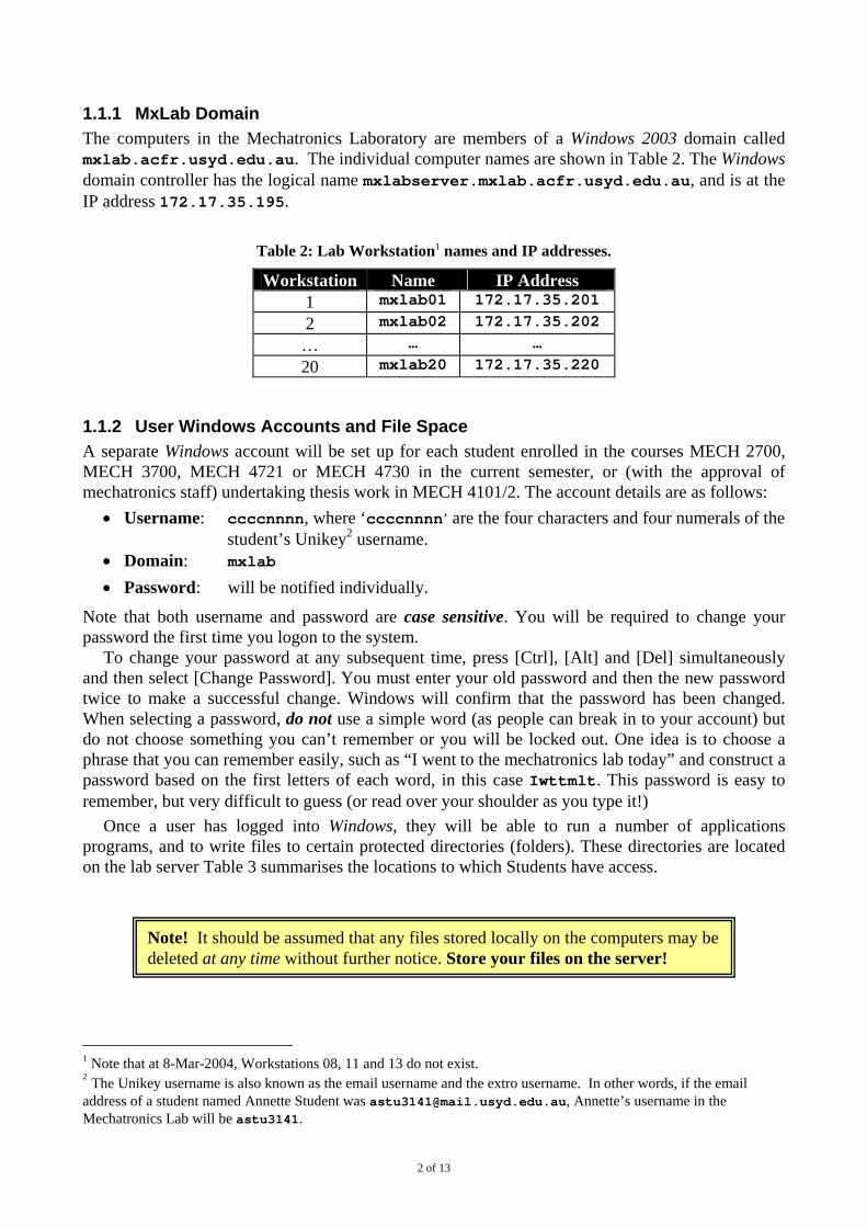
2 of 13
1.1.1 MxLab Domain The computers in the Mechatronics Laboratory are members of a Windows 2003 domain called mxlab.acfr.usyd.edu.au. The individual computer names are shown in Table 2. The Windows domain controller has the logical name mxlabserver.mxlab.acfr.usyd.edu.au, and is at the IP address 172.17.35.195.
Table 2: Lab Workstation1 names and IP addresses.
Workstation Name IP Address 1 mxlab01 172.17.35.201
2 mxlab02 172.17.35.202
… … …
20 mxlab20 172.17.35.220
1.1.2 User Windows Accounts and File Space A separate Windows account will be set up for each student enrolled in the courses MECH 2700, MECH 3700, MECH 4721 or MECH 4730 in the current semester, or (with the approval of mechatronics staff) undertaking thesis work in MECH 4101/2. The account details are as follows:
• Username: ccccnnnn, where ‘ccccnnnn’ are the four characters and four numerals of the student’s Unikey2 username.
• Domain: mxlab • Password: will be notified individually.
Note that both username and password are case sensitive. You will be required to change your password the first time you logon to the system.
To change your password at any subsequent time, press [Ctrl], [Alt] and [Del] simultaneously and then select [Change Password]. You must enter your old password and then the new password twice to make a successful change. Windows will confirm that the password has been changed. When selecting a password, do not use a simple word (as people can break in to your account) but do not choose something you can’t remember or you will be locked out. One idea is to choose a phrase that you can remember easily, such as “I went to the mechatronics lab today” and construct a password based on the first letters of each word, in this case Iwttmlt. This password is easy to remember, but very difficult to guess (or read over your shoulder as you type it!)
Once a user has logged into Windows, they will be able to run a number of applications programs, and to write files to certain protected directories (folders). These directories are located on the lab server Table 3 summarises the locations to which Students have access.
1 Note that at 8-Mar-2004, Workstations 08, 11 and 13 do not exist. 2 The Unikey username is also known as the email username and the extro username. In other words, if the email address of a student named Annette Student was [email protected], Annette’s username in the Mechatronics Lab will be astu3141.
Note! It should be assumed that any files stored locally on the computers may be deleted at any time without further notice. Store your files on the server!
3 of 13
Table 3: File Locations and Shortcuts
Location Data Type(s) Shortcut(s) \\mxlabserver\Users\3 An individual user’s files U:
My Documents (shortcut on desktop)
\\mxlabserver\Groups\4 Files shared between multiple users V: (shortcut on desktop)
\\mxlabserver\Courses\ Course specific information (shortcut on desktop) \\mxlabserver\Farnell\ Semiconductor datasheets Accessed via application C:\Documents and Settings\%USERNAME%\
Windows Profile information (desktop settings, background etc.)
none
As an example, Annette Student’s machine configuration will be in a directory (folder) named
c:\Documents and Settings\astu3141, while her files will be stored in U:\astu3141. The default permissions on these directories (and their subdirectories) will prevent any other user from viewing, copying or deleting the files. You should not change the permissions on these directories or any other folder or file within it – this may interfere with the correct operation of Windows.
Several of the applications used in the Mechatronics Laboratory do not support UNC (Universal Naming Convention) filenames (e.g. \\mxlabserver\Users), and so drive mappings are provided to the locations where data is to be stored. Please try to remember to use U: and V: preferentially over their UNC versions to avoid these problems.
1.1.3 Access to User Accounts Before you can be granted access to the computer account created for your use in the Mechatronics Laboratory you will be required to sign a written agreement to comply with the Conditions of Use of the University’s ‘Policy on the Use of University Information and Communication Technology Resources (ICT Resources).’ This document is available on the Internet at http://policy.rms.usyd.edu.au/00000ah.pdf.
1.1.4 Security Settings and “Shares” In addition to their “private” file space, students can create folders designed for storing groupwork files. Any student can create new folders within the (\\mxlabserver\Groups) folder (the V: drive) on the lab server. The default permissions for any folders created in this directory will allow the user who created the folder to have full control over the folder and all the files and folders within it. In this context, “full control” means the ability to permit or deny access by any other user.
Before they can access a particular groupwork folder, other students will need to be added to the permissions for that folder. The creator of the folder is the only user who can change the permissions of other users. The permissions for the user who created the folder do not have to be modified to allow them to use the files correctly. To change those users who have access to a folder
3 Individual users cannot create folders in this location and have access only to their own folder. Each student is provided a folder with the same name as their login name, eg. \\mxlabserver\Users\astu3141 for Annette Student. 4 Users can create folders here and set permission to allow others to access the files. See details later in this document.
Note! Please be aware that student accounts will cleared at the end of each semester. The account will be disabled, and all user files deleted.
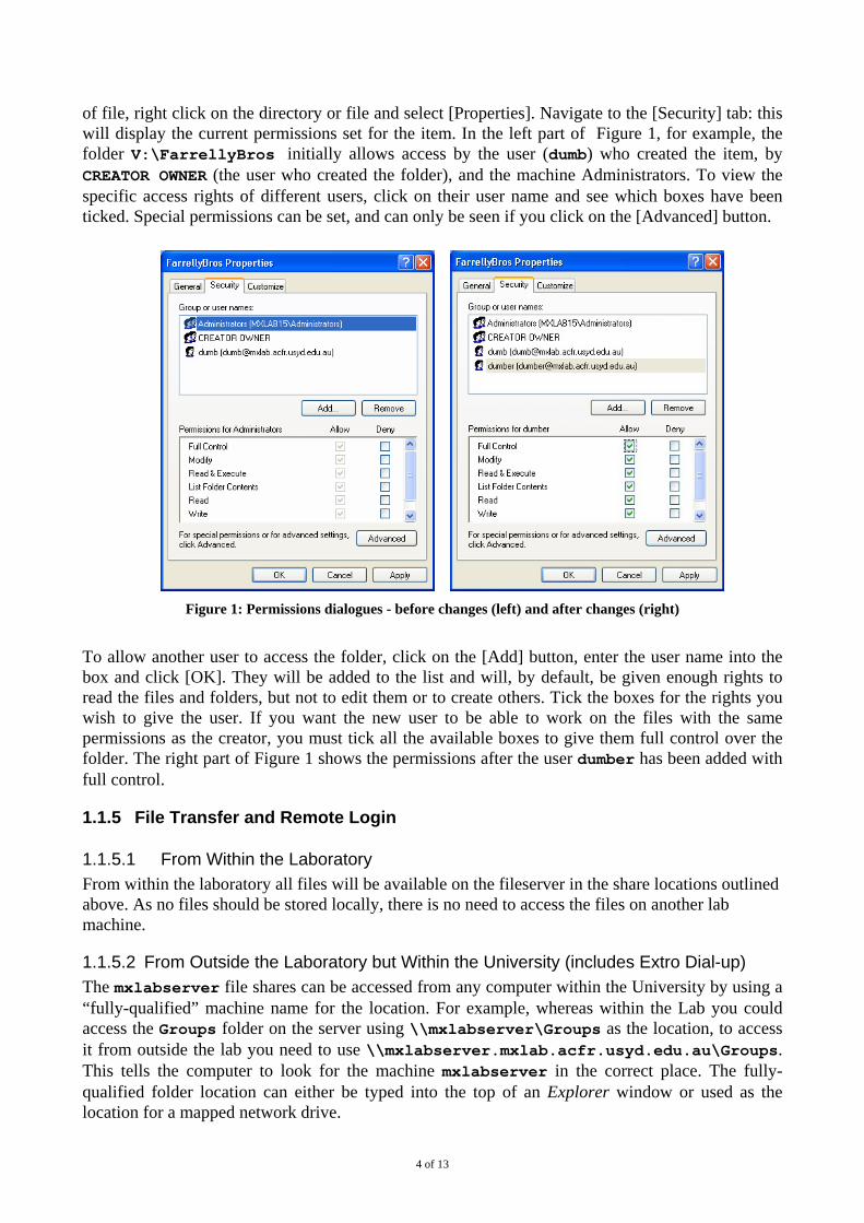
4 of 13
of file, right click on the directory or file and select [Properties]. Navigate to the [Security] tab: this will display the current permissions set for the item. In the left part of Figure 1, for example, the folder V:\FarrellyBros initially allows access by the user (dumb) who created the item, by CREATOR OWNER (the user who created the folder), and the machine Administrators. To view the specific access rights of different users, click on their user name and see which boxes have been ticked. Special permissions can be set, and can only be seen if you click on the [Advanced] button.
Figure 1: Permissions dialogues - before changes (left) and after changes (right)
To allow another user to access the folder, click on the [Add] button, enter the user name into the box and click [OK]. They will be added to the list and will, by default, be given enough rights to read the files and folders, but not to edit them or to create others. Tick the boxes for the rights you wish to give the user. If you want the new user to be able to work on the files with the same permissions as the creator, you must tick all the available boxes to give them full control over the folder. The right part of Figure 1 shows the permissions after the user dumber has been added with full control.
1.1.5 File Transfer and Remote Login
1.1.5.1 From Within the Laboratory
From within the laboratory all files will be available on the fileserver in the share locations outlined above. As no files should be stored locally, there is no need to access the files on another lab machine.
1.1.5.2 From Outside the Laboratory but Within the University (includes Extro Dial-up)
The mxlabserver file shares can be accessed from any computer within the University by using a “fully-qualified” machine name for the location. For example, whereas within the Lab you could access the Groups folder on the server using \\mxlabserver\Groups as the location, to access it from outside the lab you need to use \\mxlabserver.mxlab.acfr.usyd.edu.au\Groups. This tells the computer to look for the machine mxlabserver in the correct place. The fully-qualified folder location can either be typed into the top of an Explorer window or used as the location for a mapped network drive.
5 of 13
You can also access the files that you store on the machines in the AMME School’s computer laboratories (Rooms S322 and S345) by using File Transfer Protocol (FTP) within an Internet Explorer window. To access these files type the location ftp://172.17.35.9 into the top of an Internet Explorer window – be sure to get the slashes in the correct direction! When your computer connects, it will either log you in to the FTP server immediately (if you have logged in earlier in the session), or prompt you to enter your User name and Password. Note that these are the User name and Password for the AMME School computers, NOT for the Mechatronics Lab computers and that there is no mechanism for the transferral of password changes between the two domains.
1.1.5.3 From Outside the University
The mxlab domain exists as a private part of the University’s network and so cannot be accessed from outside the University except by
1. Using a dial-up account with Extro – or – 2. Using another ISP and connecting to the University’s VPN server – or – 3. Connecting to the University’s Wireless Network, and hence the VPN server.
If you live on campus you will be connected to a network inside the University. Given these conditions, you can access the Windows shares on either the server or on individual computers as outlined below.
If you connect to the Internet using an ISP other than the University (Extro dial-up account), try using the University’s VPN server. Apart from that, the only method for transferring files between the Lab and an outside computer is via your student email account, or on a USB drive or a floppy disk (ha!). Your email account can be reached on the web at https://www-mail.usyd.edu.au. From there, you can simply send your files to yourself as attachments to email.
Windows XP or 2000 1. Use Windows Explorer to connect by using a UNC name in the Explorer address window:
\\mxlabserver.mxlab.acfr.usyd.edu.au 2. Enter your username as mxlab\Username and password when prompted.
Linux (thanks Rob)
1. The cleanest way to access Windows shares in the mxlab from Linux is to mount the remote share, so that you can access the files on the remote system using your normal GUI file browser. You must be root to do this on most systems. Type the following on one line
mount -t smbfs -o username=Username,workgroup=mxlab //mxlabserver.mxlab.acfr.usyd.edu.au/groups /mnt/mymount/
2. The alternative is to access the remote system using smbclient. Once you have run the smbclient command with the appropriate options you will have ftp-like access to the Windows share. Type the following on one line:
smbclient //mxlabserver.mxlab.acfr.usyd.edu.au/groups -W mxlab -U Username
Of course, you will replace Username with your actual mxlab Username, won’t you…
Windows ME, 98 or 95 Get a proper operating system on your computer, and then follow the instructions above.
Macintosh We don’t know, as no one here uses a Mac. If anyone does know, please tell us.
6 of 13
1.1.6 Virus Protection Each PC is protected by Symantec Antivirus, which is configured to intercept and quarantine viruses. Virus definitions are automatically updated as they become available from Symantec, and each machine is scanned daily.
1.1.7 Windows Updates and Patches Each machine in the laboratory is connected to an automatic updating service. This means that operating system patches are automatically installed. Together with the automated virus updateing and scanning, this represents current “best practice” for avoiding virus or other attacks.
1.1.8 Printing There are no printers in the Mechatronics Lab. Undergraduate students who have accounts in the domain uglab.aeromech.usyd.edu.au can print to the printers hosted in that domain. The printers are physically located in Rooms S322 and S345 in the Mechanical Engineering Building.
1.1.9 Running DOS Application Software Some of the applications programs run from a command line prompt within a DOS shell5. Each of these DOS application is run by a batch file that is in the subdirectory C:\Bat of each machine. This directory is in the Windows PATH variable of every user, so that each console application can be executed from any user directory. Each batch file does a number of things:
• SETs any environment variables required by the particular application; • sets a PATH suitable for the application; • runs the application, and then; • resets PATH to the value it had before the batch file was run; • clears any environment variables that were SET.
1.1.10 Personal Batch Files If you want to create and use your own batch files, your batch files must do at least the following two things before they terminate, even if they terminate with errors:
1. clear any environment variables that are SET by the batch file; 2. reset PATH to its value before the batch file.
1.1.11 Computer and Network Maintenance The computers and network in the Mechatronics Lab are configured and maintained by staff from the Australian Centre for Field Robotics. If you discover computer or network faults, please report them by email to [email protected].
1.2 Oscilloscopes Each Lab Workstation is equipped with Tektronix TDS 1002 two-channel digital storage oscilloscope, shown in Figure 2. These oscilloscopes have a bandwidth of 60MHz, and a sampling rate of 1 GS/sec. They are excellent (and expensive) tools. Please note that the scope probes (leads) are never left in the Lab. When you need to use a scope, you will have to check out one or two scope probes.
5 They are “console applications”

7 of 13
Figure 2: Front panel of a Tektronix TDS 1002 oscilloscope.
It is most important for you to learn to use a scope properly, and to get into the habit of using a scope to monitor signals. The amount of information that you can obtain from a scope is far greater than that available from a DMM6. You are expected to learn how to use a scope proficiently. If you can't use a scope effectively, read the Shortish Guide to Using an Oscilloscope, available in PDF form from the Lab website, http://www.acfr.usyd.edu.au/teaching/mxlab/. In fact, we insist that you read it anyway, before using the scope. The full TDS 1002 oscilloscope manual is also available in PDF form from the Lab web site.
1.3 Power Supplies Each Lab Workstation is equipped with a power supply having two independent sections. The front panel of the power supply is shown in Figure 3. Each unit has two independent supplies: a regulated supply for powering computers and electronics, and an unregulated supply for powering motors. The ratings of the two supplies are given in Table 3.
Figure 3: Front panel of the Mechatronics Lab bench power supplies.
Table 3: Lab power supplies - terminals and their ratings.
Unregulated Supply (to the left) Regulated Supply (to the right) • Black Terminals: +0V DC return
• White Terminals: +12V DC, 1.5 A • Yellow Terminals: –12V DC, 1.5 A
• Black Terminals: +0V DC return • Red Terminals: +5V DC, 2 A • White Terminals: +12V DC, 200mA • Yellow Terminals: –12V DC, 200mA
6 Digital multimeter.

8 of 13
There are two important things to note about the power supplies: • The +0V DC terminals of the regulated supply and the unregulated supply will be at different
potentials unless you connect them together. • All outputs of the two supplies are protected by Polyfuses. A polyfuse is a resistive element
with a positive temperature coefficient. When it heats up (due to internal I2R losses in an overcurrent state) its resistance increases by several orders of magnitude in a few hundred milliseconds, limiting current flow. If a power supply output voltage should go to zero, turn off the power supply and wait for a minute or two. The Polyfuse should reset automatically.
2 Closed Facilities – Hand Tools and Test Instruments A number of hand tools and electronic test instruments are available for you to use as required. This section contains notes on the function, and safe usage of most of the instruments. Please read carefully, and if in doubt, ask. Operating manuals are available for all of the instruments, and must be read before operating any instrument that you are unfamiliar with.
2.1 Loan Procedure To use any of the Lab’s “closed facilities” you must first borrow them. To borrow any of the resources, approach a course Tutor or Lecturer, and ask. If the resource is available for loan, it will be exchanged for some form of identification provided by you. Any additional resources that you borrow will also be associated with your identification. When you have returned all of the resources on loan to you in good condition, you may have your identification back.
2.2 Oscilloscope Probes These are good quality scope probes which will cost you $218.00 (each probe) to replace if you lose or damage them through either misuse or misbehaviour. They are to be used only for probing circuits. Please be careful and treat them gently.
2.3 Toolkits Toolkits are available for loan to students as required, but may not be taken out of the Lab. Each toolkit contains:
• Digital multimeter with 2 probes (see notes in section 2.4) • Wire cutters: for cutting copper wire only, up to 0.8 mm diameter. Do not use to cut steel
wire, such as paperclips. With a little practice, these can also be used to strip insulation from wires quickly.
• Wire strippers: designed for stripping plastic insulation from wires. • Flat jaw pliers: for bending and forming component leads, and holding stuff. • Small flat screwdriver: for screw terminals on some boards, and for lifting ICs from
sockets and solderless breadboard. • IC extraction tool: don’t lift ICs out of solderless breadboard with your fingers – you will
end up with a row of holes in your thumb, and bent IC leads! • Test leads (1 set): for connecting to PCB headers or sockets. • Power leads (1 set), or Plug pack, depending on the work that you are doing.
A tool kit will generally be loaned for one lab session only. Any tools missing or damaged through misuse when the tool kit is returned must be replaced at the expense of the student who borrowed the toolkit.
9 of 13
2.4 Digital Multimeter (in toolkits) The digital multimeter, or DMM, is a versatile multi-purpose test instrument that can measure DC and AC voltage, current, resistance, etc. To use, turn on; set function (volts, ohms, etc.) to the highest range, to minimise the risk of damage. Touch probes to circuit under test; reduce range as appropriate. Turn the meter off when you have finished with it, to conserve batteries.
Some cautions about using DMMs:
• A DMM is a static instrument – it shows only a stationary or time-averaged reading, and cannot show a signal changes with time. For this reason, DMM readings can often be misleading. Take a little time to learn to use an oscilloscope correctly – it is quite simple.
• The principal use of a DMM is measuring quantities that are known to be constant in time – checking component values, setting DC voltages, etc.
• Measure voltage differences with the meter in parallel to the circuit to be measured, and current with the meter in series with the circuit.
• A DMM measures resistance by injecting a small, known, current into the circuit under test. You must therefore be cautious whan attempting to measure the resistance of a device that is in a circuit, and when interpreting the “resistance” reading displayed by the meter. You may need to remove (one leg of) the device from the circuit to measure the resistance.
• Never measure a voltage with the DMM set on Ohms – this will destroy the DMM. For example, never try to measure the resistance of a battery!!!
• Never measure the “resistance” of an IC – it just doesn’t make sense… • The integrity of a diode can be tested using a DMM set to the lowest resistance range. Recall
that a diode conducts when forward biased, and not when reverse biased, so that the “resistance” of a diode should be very large in one direction and very small in the other.
• A BJT is really just two diodes in one package with three leads…
2.5 Solderless Breadboards These are used for rapidly prototyping circuits. Reasonable results can be achieved, although the significant capacitance of the breadboard itself, and the (often long) wires used in prototyping mean that breadboards are not useful for high-speed or low-noise circuits. They also cannot be used for power circuitry.
2.5.1 Rules for Breadboard Use • Use only single-core insulated wire, with a core diameter of 0.7 mm ("bell wire"). If multi-
stranded wire is used, strands break off inside the breadboard, causing short circuits and trouble for us all.
• Never force oversize component pins (e.g. wire-wrap sockets) into the sockets. This permanently damages the sockets, and each breadboard costs about $85 (!!).
• Never breadboard circuits that contain discrete or IC power components such as power transistors, regulators, etc. The breadboard will be damaged by the heat generated by the I2R losses where the component leads are inserted.
DANGER! The multimeters that are provided in the Lab toolkits are inexpensive models that are not designed for industrial use. Never use them for measuring 240V AC mains electrical circuits.
10 of 13
2.5.2 Breadboarding a Circuit • First, draw a circuit diagram showing all components, signal names and pin numbers. A
good circuit diagram will simplify the wiring, and help immensely with troubleshooting. • Think about the placement of all components before you start to build the circuit, then place
all components. Place the ICs with pin 1 oriented in the same direction (usually the top left corner). Do not forget to place any mass termination connector(s) required. Place connectors and trim pots near the outside of the breadboard for ease of access.
• Establish power supply buses (+0V, +5V, plus ±12V if required) by connecting the long lines on the sides of the breadboard to the binding posts. In the Lab we use the colour code
• Red: + 5V DC • White: +12V DC • Black: + 0V DC • Yellow: –12V DC.
• Establish power supply to all devices. This will help your orientation in the circuit, and will ensure that you do not forget to power a device. Use the same wire colours as above. Do not forget to add sufficient bypass capacitors (0.01 to 0.1 µF tantalum chip capacitors).
• Connect the other signals: data, address, I/O lines. Use different colours to help in tracing and troubleshooting the circuit. For example, data bit 0 is blue, bit 1 is green, etc.
• Check the whole circuit.
2.5.3 Initial Power-up • Check the whole circuit again. • Set any trim pots to sensible starting values, usually mid-range if the circuit design is
sensible. • Power the circuit up, ensuring that all voltages (+0V, +5V, ±12V if required) are applied
simultaneously. Carefully touch the component packages (not the leads) to check that none of the chips are overheating. Switch off immediately if any temperatures seem excessive.
• If everything is OK so far, check all the power supply pins with an oscilloscope to make sure that power is available everywhere it should be. Use the scope so that you can see time-varying signals (e.g. noise) if they are present! Check to see if clock pulses are present everywhere that they should be.
• Finally, apply valid input signals, and start to check that everything is working properly.
2.6 Crimp Tool We use the AMP “Modu” type crimp contacts and contact carriers for some semi-permenant project work in the Lab. Several hand-operated crimp tools are available to make these connectors. You will need a small amount of instruction on the easiest way to use this tooling.
2.7 Logic Probe A logic probe is a simple test instrument that senses the logic state of a circuit node.
To use a logic probe, first connect the black lead to +0V DC, then the red lead to +5V DC power source. Touch the probe to a point in the powered-up TTL logic circuit: the LEDs & audiable tone indicate the logic state (high, low, or pulsing) at that point in the circuit.
CAUTION! Power up the circuit first! Logic probes have a (small) potential to damage the circuit under test if the circuit is not powered up during testing.

11 of 13
2.8 Logic Pulser A logic pulser is a test instrument that senses the logic state (high or low) at a circuit node, and injects a pulse of the opposite logical state into the circuit. The pulse injected can be either a single pulse, or a 5 Hz pulse train. A logic pulser is useful for injecting exactly one pulse into a circuit (no switch bounce) or for tracing a signal through a board.
To use, first connect black lead to +0V DC, and the red lead to +5V DC power source. Touch the probe tip to a powered-up TTL logic circuit, and press the button.
2.9 Function Generator We have several Hung Chang model 8205A Sweep Function Generators. These can generate frequency-swept or stationary square, sine or triangle waves at frequencies up to 2MHz. They are useful for generating quick-and-dirty signals, but are not stable enough to act as clocks, etc.
2.10 Frequency Counter We have a Yokagawa FC-863 Frequency Counter.
2.11 Ango EPROM Eraser This device consists of an ultraviolet tube mounted above a small sliding tray. To erase a (UV) EPROM, remove any label from the quartz window and place the EPROM in the tray, with its legs pushed into the conductive foam. Turn on the eraser. The eraser will erase (set all bits to 1) a few EPROMs in about 40 minutes. Some cautions:
• Don't look at the UV radiation – it can permanently damage the eye; • Turn the eraser off at the power when finished.
2.12 Sunshine Expro-60 Universal Device Programmer and Tester This instrument is controlled from a PC that runs DOS. The program will start when the PC is booted. It and allows EPROMs and other logic devices (PALs, etc.) to be programmed ("blown"). It can perform functional (but not timing) tests of TTL devices from the 74xx family (including 74HCxx), and CMOS devices from the 40xx and 45xx families. It can also identify unknown TTL devices. You might need a short driving lesson before operating it because some of the menus are a bit cryptic.
Some cautions in using the programmer: • Make sure that you place the device to be programmed or checked in the correct place in the
ZIF (zero insertion force) socket, and close the ZIF socket by pushing the handle. Warning: A wrongly-positioned device will usually be destroyed during programming.
• Some otherwise equivalent EPROMs from different sources (manufacturers) require different programming voltages (Vpp). If you are not sure what the manufacturer's recommended programming voltage is, start at the lowest voltage.
3 Electronic Components We keep a small stock of passives (resistors, capacitors, etc.), analogue (so-called “linear”) devices (transistors, op-amps, timers, comparators), digital ICs (particularly 74LSxx, 74HCxx, 74ACxx, and some 74xx family ICs), optoelectronics (LEDs, 7-segment displays), and some hardware (push buttons, switches, etc.). Most of the components that we keep are listed on the Lab web site, along with links to data sheets in PDF format.

12 of 13
If you need to use components, identify what you will need, then speak to a Tutor or Lecturer. You may be asked to justify your selection with a circuit diagram and/or design calculations. When using components from our stock, please:
• If you find that you don’t need to use something, give it to a Tutor or Lecturer to go back in the component bins straight away. Otherwise, it will get kicked around on the bench and, eventually, thrown out.
• When you blow something up, own up!! Don’t worry – we’ve done it too... If the chip is testable (TTL logic gates, RAM), use the Expro 60 tester to check. If the chip is dead, fold its legs over and throw it away. Never allow a dead component to be put back into the component bins – you mabe the unfortunate person who takes it out to use!!
3.1 Static and Component Handling Precautions Some ICs are static-sensitive, and can be destroyed through careless handling. Even worse, static damage is cumulative – damage that occurs in handling may not be enough to destroy the device, but a small amount of additional damage may end the device’s life. This scenario is particularly disasterous if it occurs in the field during the warranty period… You should be particularly careful with analogue CMOS – A/D converters are especially prone to damage. Before handling a static-sensitive device, you should touch your hand to ground, or at least to a large capacitance, to discharge any accumulated static. Once the device is in a circuit and powered, no special precautions need be taken.
Aside: Actually, one should use a conductive wrist strap earthed through a 1M resistor, together with conductive tools & work surface. This is done in production. Also, while we are talking about production, be aware that static damage is cumulative. If the proper anti-static precautions are not taken, a chip can get “zapped” during assembly, but still function well enough to pass testing. It gets delivered in a product, and then fails in the field. Ouch.
3.2 Importance of Power Supply Another way that a chip may be destroyed is to apply an input (analogue or digital) before the chip’s power supply is established. In particular, if you apply an input to an op-amp before both (+ and –) power supplies are connected, or if the supply voltages are unequal, the op-amp may be destroyed when the input voltage exceeds either of the op-amp’s power supply rail voltages. This is one good reason for always connecting the power supply first when bread boarding a circuit.
4 Components Data Sheets and Reference Manuals When working with electronics, the only reliable reference is the device manufacturer's data sheets, and even then you need to be careful. All component manufacturers provide data sheets on their web sites, invariably in Adobe portable document format (PDF). We have tried to provide links on the Lab web site to data sheets for each device that you are likely to use. You will have to become very familiar with reading these data sheets.
Some other resources include: • PDF data sheets held on the Lab file server. These can be accessed through the Programs
menu on each Lab computer. • Component reseller's catalogues (and web sites) – Farnell Components, RS Components,
Jaycar Electronics, Altronics, Dick Smith Electronics. These have a lot of useful information in them. See in particular the information in the back of the Dick Smith catalogue.
13 of 13
• Component manufacturer’s web sites – these are linked from the Mechatronics Lab web site, http://www.acfr.usyd.edu.au/teaching/mxlab/.
5 Document Improvement Should you discover errors, omissions or unclear information in this document, please report these deficiencies by email to [email protected] so that this document can be improved. David Rye, Richard Grover, Steve Scheding July 2002
Revised March 2004 Revised April 2003