Embed Size (px)
Citation preview
Computer EngineeringMekelweg 4,
2628 CD DelftThe Netherlands
http://ce.et.tudelft.nl/
2007
MSc THESIS
High speed reconfigurable computation forelectronic instrumentation in space applications
Dimitrios Lampridis
Abstract
Faculty of Electrical Engineering, Mathematics and Computer Science
CE-MS-2007-20
Small, light structures, with low power consumption are the key tosuccess for future electronic instrumentation in space applications.Future missions will have to rely on lighter payloads to reduce thecosts, and higher levels of integration to put more instruments inthe confined space of a small spacecraft. At the same time, re-cent developments in the space industry have introduced radiation-hardened FPGAs, making one step forward towards the use of re-programmable hardware in space, and the European Space Agencyis actively promoting System-on-Chip (SoC) design methodologiesfor future highly-integrated space electronics. In this thesis, we setoff to investigate the benefits of a managed SoC approach in futurespace electronic instrumentation. To this end, we study a digitalpulse detector. Such an instrument is often found on-board on plan-etary exploration spacecrafts, because of its two-fold role: its pri-mary function is to monitor the radiation levels of the spacecraft’senvironment, but it can also classify the detected radiation pulses toperform γ-ray digital spectroscopy. The pulse detector is designedas an AMBA IP core that can be interfaced to many SoC libraries.We perform all processing associated to pulse detection, includingshaping, pulse height determination, and pile-up rejection, in real-
time with zero dead-time. To achieve this, we use a shallow-pipelined serial design, with a spesialisedcomputational block for digital trapezoidal shaping, based on Carry-Save Adder reduction trees, followedby a custom peak detection algorithm. Our pulse detector is able to maintain a constant high throughputand low latency, independent of the number of samples under consideration. Additionally, the entire pulsedetection mechanism is supervised by the on-chip processor through embedded software. We developed aprototype using a Xilinx XC3S1500 FPGA, the LEON3 on-chip processor and a set of IP cores from theGRLIB library. An external 8-bit ADC and the pulse detector were clocked at 100MHz, while the rest ofthe system was running at 40MHz. Preliminary experimental results obtained with our prototype are verypromising and demonstrate the correctness of the design.


High speed reconfigurable computation forelectronic instrumentation in space applications
empty
THESIS
submitted in partial fulfillment of therequirements for the degree of
MASTER OF SCIENCE
in
COMPUTER ENGINEERING
by
Dimitrios Lampridisborn in Athens, Greece
Computer EngineeringDepartment of Electrical EngineeringFaculty of Electrical Engineering, Mathematics and Computer ScienceDelft University of Technology


High speed reconfigurable computation forelectronic instrumentation in space applications
by Dimitrios Lampridis
Abstract
Small, light structures, with low power consumption are the key to success for future elec-tronic instrumentation in space applications. Future missions will have to rely on lighter payloadsto reduce the costs, and higher levels of integration to put more instruments in the confined spaceof a small spacecraft. At the same time, recent developments in the space industry have intro-duced radiation-hardened FPGAs, making one step forward towards the use of reprogrammablehardware in space, and the European Space Agency is actively promoting System-on-Chip (SoC)design methodologies for future highly-integrated space electronics. In this thesis, we set off toinvestigate the benefits of a managed SoC approach in future space electronic instrumentation.To this end, we study a digital pulse detector. Such an instrument is often found on-board onplanetary exploration spacecrafts, because of its two-fold role: its primary function is to monitorthe radiation levels of the spacecraft’s environment, but it can also classify the detected radia-tion pulses to perform γ-ray digital spectroscopy. The pulse detector is designed as an AMBAIP core that can be interfaced to many SoC libraries. We perform all processing associated topulse detection, including shaping, pulse height determination, and pile-up rejection, in real-timewith zero dead-time. To achieve this, we use a shallow-pipelined serial design, with a spesialisedcomputational block for digital trapezoidal shaping, based on Carry-Save Adder reduction trees,followed by a custom peak detection algorithm. Our pulse detector is able to maintain a constanthigh throughput and low latency, independent of the number of samples under consideration. Ad-ditionally, the entire pulse detection mechanism is supervised by the on-chip processor throughembedded software. We developed a prototype using a Xilinx XC3S1500 FPGA, the LEON3on-chip processor and a set of IP cores from the GRLIB library. An external 8-bit ADC and thepulse detector were clocked at 100MHz, while the rest of the system was running at 40MHz. Pre-liminary experimental results obtained with our prototype are very promising and demonstratethe correctness of the design.
Laboratory : Computer EngineeringCodenumber : CE-MS-2007-20
Committee Members :
Advisor: Sorin D. Cotofana, CE, TU Delft
Member: Rene van Leuken, CAS, TU Delft
i

Member: Stefan Kraft, cosine Research BV
ii

To someone...
iii

Contents
List of Figures vi
List of Tables vii
Acknowledgements viii
1 Introduction 1
2 Background & Related Work 42.1 Trapezoidal Filtering . . . . . . . . . . . . . . . . . . . . . . . . . . . . . . 42.2 Dual-Channel Filters . . . . . . . . . . . . . . . . . . . . . . . . . . . . . . 62.3 Related Work . . . . . . . . . . . . . . . . . . . . . . . . . . . . . . . . . . 7
3 System Architecture 93.1 Architectural Overview . . . . . . . . . . . . . . . . . . . . . . . . . . . . 93.2 Filter Datapath . . . . . . . . . . . . . . . . . . . . . . . . . . . . . . . . . 10
3.2.1 Operand Selection . . . . . . . . . . . . . . . . . . . . . . . . . . . 123.2.2 Filtering Calculation . . . . . . . . . . . . . . . . . . . . . . . . . . 143.2.3 Peak Detection . . . . . . . . . . . . . . . . . . . . . . . . . . . . . 16
3.3 AMBA Control Block . . . . . . . . . . . . . . . . . . . . . . . . . . . . . 183.4 Multiple Clock Domains . . . . . . . . . . . . . . . . . . . . . . . . . . . . 20
4 Experimental Setup & Results 234.1 GRLIB IP Core Library . . . . . . . . . . . . . . . . . . . . . . . . . . . . 23
4.1.1 The LEON3 Processor . . . . . . . . . . . . . . . . . . . . . . . . . 244.1.2 Plug & Play Capability . . . . . . . . . . . . . . . . . . . . . . . . 244.1.3 PC Interface . . . . . . . . . . . . . . . . . . . . . . . . . . . . . . 25
4.2 Development Board . . . . . . . . . . . . . . . . . . . . . . . . . . . . . . 264.2.1 The Mezzanine Board . . . . . . . . . . . . . . . . . . . . . . . . . 264.2.2 Clock Distribution . . . . . . . . . . . . . . . . . . . . . . . . . . . 27
4.3 Pulse Generation . . . . . . . . . . . . . . . . . . . . . . . . . . . . . . . . 284.4 Development Tools . . . . . . . . . . . . . . . . . . . . . . . . . . . . . . . 294.5 Results . . . . . . . . . . . . . . . . . . . . . . . . . . . . . . . . . . . . . . 30
4.5.1 Area . . . . . . . . . . . . . . . . . . . . . . . . . . . . . . . . . . . 304.5.2 Performance . . . . . . . . . . . . . . . . . . . . . . . . . . . . . . 304.5.3 Histograms . . . . . . . . . . . . . . . . . . . . . . . . . . . . . . . 32
iv

5 Conclusion 345.1 Problems Encountered . . . . . . . . . . . . . . . . . . . . . . . . . . . . . 355.2 Lessons Learned . . . . . . . . . . . . . . . . . . . . . . . . . . . . . . . . 365.3 Further Work . . . . . . . . . . . . . . . . . . . . . . . . . . . . . . . . . . 37
Bibliography 40
A List of registers 41A.1 Configuration/Status register . . . . . . . . . . . . . . . . . . . . . . . . . 41A.2 Slow filter configuration register . . . . . . . . . . . . . . . . . . . . . . . . 42A.3 Fast filter configuration register . . . . . . . . . . . . . . . . . . . . . . . . 42A.4 Slow filter thresholds register . . . . . . . . . . . . . . . . . . . . . . . . . 43A.5 Fast filter thresholds register . . . . . . . . . . . . . . . . . . . . . . . . . 43A.6 Result register . . . . . . . . . . . . . . . . . . . . . . . . . . . . . . . . . 44
B Sample embedded C code 45
v

List of Figures
2.1 Segmentation of input samples for trapezoidal filtering . . . . . . . . . . . 52.2 Simulated filter response for various inputs . . . . . . . . . . . . . . . . . 62.3 Pile-up inspection using dual-channel filtering . . . . . . . . . . . . . . . . 7
3.1 IP core functional diagram . . . . . . . . . . . . . . . . . . . . . . . . . . . 93.2 Selection of operands from FIFO memory . . . . . . . . . . . . . . . . . . 123.3 Three-stage pipelined design of the filter datapath . . . . . . . . . . . . . 133.4 First pipeline stage: operand selection . . . . . . . . . . . . . . . . . . . . 143.5 Six-to-two CSA reduction tree with two inverted operands . . . . . . . . . 153.6 Second pipeline stage: filtering calculation . . . . . . . . . . . . . . . . . . 163.7 Third pipeline stage: peak detection . . . . . . . . . . . . . . . . . . . . . 173.8 Peak detection finite state machine . . . . . . . . . . . . . . . . . . . . . . 183.9 Block diagram of the AMBA interface . . . . . . . . . . . . . . . . . . . . 193.10 AMBA APB read and write bus cycles . . . . . . . . . . . . . . . . . . . . 193.11 States and transitions of the AMBA control block . . . . . . . . . . . . . 203.12 Four-phase handshaking protocol . . . . . . . . . . . . . . . . . . . . . . . 213.13 Set of cross-clock domain signals . . . . . . . . . . . . . . . . . . . . . . . 22
4.1 Complete System-On-Chip block diagram . . . . . . . . . . . . . . . . . . 244.2 GRLIB APB slave input/output records . . . . . . . . . . . . . . . . . . . 254.3 Typical GRLIB APB slave entity definition . . . . . . . . . . . . . . . . . 254.4 Top view of the development board . . . . . . . . . . . . . . . . . . . . . . 274.5 Development board with fitted mezzanine . . . . . . . . . . . . . . . . . . 274.6 Clock distribution network . . . . . . . . . . . . . . . . . . . . . . . . . . . 284.7 Post-Map FPGA resource utilisation . . . . . . . . . . . . . . . . . . . . . 314.8 XC3S1500 Spartan3 FPGA resource usage . . . . . . . . . . . . . . . . . . 314.9 Timing report . . . . . . . . . . . . . . . . . . . . . . . . . . . . . . . . . . 324.10 Pulse height distribution histograms for one million events from a Cobalt-
60 source . . . . . . . . . . . . . . . . . . . . . . . . . . . . . . . . . . . . 33
vi

List of Tables
A.1 Configuration/Status register, offset 00000H . . . . . . . . . . . . . . . . . 41A.2 Slow filter configuration, offset 00001H . . . . . . . . . . . . . . . . . . . . 42A.3 Fast filter configuration, offset 00010H . . . . . . . . . . . . . . . . . . . . 42A.4 Slow filter thresholds, offset 00011H . . . . . . . . . . . . . . . . . . . . . 43A.5 Fast filter thresholds, offset 00100H . . . . . . . . . . . . . . . . . . . . . . 43A.6 Result register, offset 00101H . . . . . . . . . . . . . . . . . . . . . . . . . 44
vii

Acknowledgements
This text is the result of more than nine months of work that was carried out as partialfulfillment for a degree of Master of Science in Computer Engineering. During thesemonths I have spent most of my time at cosine Research BV in Leiden (yes, there isno capital letter in the word “cosine” ), and I would like to take the opportunity toacknowledge all the support that I received while doing my research at their premises.
I would like to thank in particular Alex Palacios and Erik Maddox, my on-site super-visors. Alex has been a tremendous help during the course of this work, and he offeredinvaluable advice in the design of the electronics. Erik on the other hand, provided allthe necessary background in γ-ray spectroscopy, and made me appreciate a bit more thefield of high-energy physics. Both of them were always there when I needed them, fortechnical support, but also as friends.
I would also like to thank Stefan Kraft, general manager of cosine Research BV, forgiving me the chance to work on this project and placing his faith on me, as well asproviding support and advice in critical moments of the project. Last but not least, Iwould like to thank every single employee of the company for making me feel like homefrom the very first day, and accepting me as equal among equals.
My gratitude goes to my dear professor and advisor Sorin Cotofana, for supportingmy decisions all the way, even when I contradicted myself. I do believe that his patiencewith me has been ...monumental. Thank you Sorin for letting me do my own, but alsofor pushing the “right buttons” to keep me on track.
Having said that, I would have never reached my goal if it wasn’t for the unconditionallove of my family and my beloved girlfriend, so my greatest “thank you” goes to them,for simply making me feel alive.
As far as the dedication is concerned, it was while I was working on this project, thatthe Computer Engineering laboratory of TU Delft suffered the very sudden loss of ourbeloved professor Stamatis Vassiliadis. Stamatis has been a great man and scientist, atrue inspiration from the first time that we met. I would have promptly dedicated mywork to his memory, but I believe that he deserves much more than my master thesis. Iprefer to leave the dedication empty, and honour him in my own way.
Dimitrios LampridisDelft, The NetherlandsNovember 20, 2007
viii

Introduction 1Small, light structures with low power consumption are the key to success for electronicinstrumentation in space applications [19]. Lighter payloads reduce the mission costsand allow us to put more instruments in the confined space of a small spacecraft.
In the future, the ever-increasing demands for high processing performance, low massand power on board the spacecraft, will demand for very high integration levels of in-strumentation and electronics. Following the current trends in the rest of the electronicsindustry, as the number of available resources on silicon increases, the design of electronicinstrumentation for space applications will have to move away from the use of traditionalcomponents to more advanced and complex systems within a single device [17].
To develop such complicated multi-functional systems the design methodology willhave to change from being gate-level oriented to the integration of complex buildingblocks, with verified functionality. These blocks should also be accompanied by detaileddocumentation and testing methodology.
As the number of instruments on-board the spacecraft increases, so does the amountof data generated during the mission. It is highly unlikely that the slow down-link fromthe spacecraft to Earth will be able to transfer all this information in time. Furthermore,apart from their scientific purpose, many of the on-board instruments play a vital, safety-critical role in the spacecraft’s reaction to the environment and need real-time processing.The solution is to do on-board processing, in order to reduce the amount of output data,and to respond faster to environmental changes.
System-on-Chip (SoC) approaches offer a small, light single-chip solution, fitting theabove-stated requirements of high integration, managed design methodology with largebuilding blocks, and on-board processing. An SoC is usually developed using FieldProgrammable Gate Arrays (FPGAs), but the final product can also be manufacturedinto an Application Specific Integrated Circuit (ASIC).
With the capacity and performance of FPGAs increasing every year, and the manu-facturing costs of an ASIC still very high, it is becoming a popular solution to actuallyfly the FPGAs in space, instead of just using them during design development only.The role of the FPGAs is also rapidly changing, from simple “glue” logic between othersilicon chips, to a complete SoC, comprising of processors, peripherals, memories, anddedicated hardware.
Reprogrammable FPGAs offer a new dimension for space applications, because theyallow the modification of on-board electronics during the mission. Possible utilizationsof the FPGA reprogramming ability include replacing of faulty design modules, updatesto processing algorithms, adaptation to new mission requirements, and switching todifferent operation profiles, optimized for area, power, performance or a combination ofthe above.
Programmable hardware has been flying on board spacecrafts for more than a decade.
1

2 CHAPTER 1. INTRODUCTION
However, most of the FPGAs used are still one-time programmable, because repro-grammable FPGAs are more sensitive to involuntary reconfiguration due to Single EventUpsets (SEU) induced by radiation [7]. The space environment is very hostile, and highamounts of radiation can cause bit flips in memory elements. This poses an additionalthreat to the on-chip configuration memory of reprogrammable FPGAs.
Recent developments in the defense and space industry have introduced radiation-hardened FPGAs, making one step forward towards the use of reprogrammable hardwarein future space missions. Space applications present new challenges in the use of recon-figurable computing, particularly due to the effects of incident radiation, and a new fieldis emerging to provide answers and solutions.
In this thesis, we set off to investigate the benefits of a managed SoC approachin future space electronic instrumentation. For our investigation, we choose a high-count digital pulse detector. Such an instrument is often found on board planetaryexploration spacecrafts, because of its two-fold versatile role: its primary function is tomonitor the radiation levels of the spacecraft’s environment. The system continuouslymonitors the levels of the detected radiation pulses, and sends out an alarm signal tothe spacecraft when the irradiation becomes too intense and threatens the spacecraft’sintegrity. This kind of application is time-critical and demands for high responsiveness.With minor modifications, namely the recording and classification of the detected pulseheights, the instrument may also be extended with the secondary function of γ-ray digitalspectroscopy. This kind of spectroscopy is very popular in planetary missions, becauseγ-ray sensing is an established technique to study the composition of the outer layers ofplanets.
We follow a reconfigurable approach, suitable for SoC design, to process the digitizedsignals and calculate the pulse height. The digital pulse detector is designed as anAMBA [9] IP core that can be combined with other cores (processors, memories, otherperipherals) into a single SoC solution. We keep the computational part of our designseparated from the AMBA interface, within different clock domains, to remove the needfor matching the speed of the computation with that of the interconnection bus, and tomaximize the reusability of the IP core.
Our approach combines the high performance of dedicated computational hardware,with the flexibility of a complementary on-chip processor, to produce a complete, com-pact solution for future electronic instrumentation in space applications. The only partsof the system that are external to the FPGA are the analog pre-amplification and theAnalog-to-Digital Converter (ADC).
Inside our pulse detector IP core, linear trapezoidal filtering is applied to the digitizedsamples. The filters can keep a high and constant throughput, independent of the num-ber of past samples under consideration. The filtered output is further processed by asmart on-line peak detection algorithm that discards false events and pile-ups. Both thefilter and peak detector parameters are fully configurable via the AMBA APB interface.The detected peaks are transferred back to the on-chip processor, where the embeddedsoftware creates pulse height histograms and transmits them back to base.
The design was implemented in IEEE-compliant VHDL, without any manufacturer-specific hardware structures and macros, allowing us to synthesise and place the IPcore into any of the available FPGAs. For experimental purpose we programmed the
3
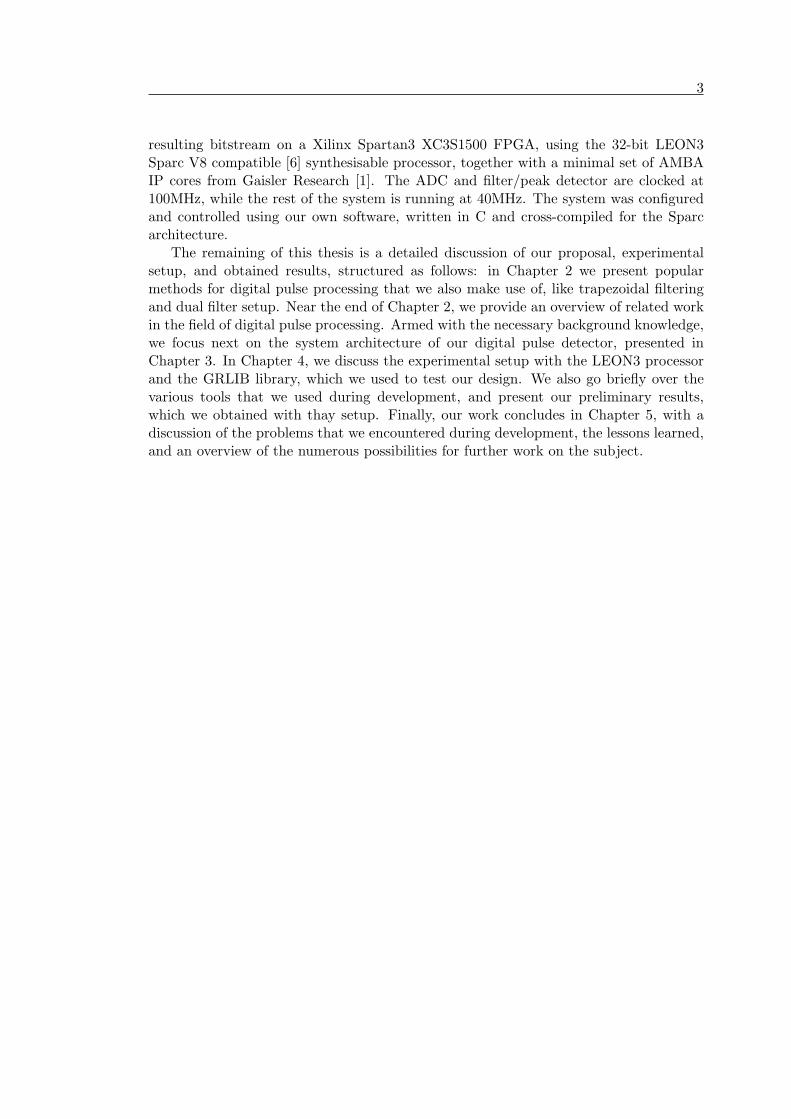
resulting bitstream on a Xilinx Spartan3 XC3S1500 FPGA, using the 32-bit LEON3Sparc V8 compatible [6] synthesisable processor, together with a minimal set of AMBAIP cores from Gaisler Research [1]. The ADC and filter/peak detector are clocked at100MHz, while the rest of the system is running at 40MHz. The system was configuredand controlled using our own software, written in C and cross-compiled for the Sparcarchitecture.
The remaining of this thesis is a detailed discussion of our proposal, experimentalsetup, and obtained results, structured as follows: in Chapter 2 we present popularmethods for digital pulse processing that we also make use of, like trapezoidal filteringand dual filter setup. Near the end of Chapter 2, we provide an overview of related workin the field of digital pulse processing. Armed with the necessary background knowledge,we focus next on the system architecture of our digital pulse detector, presented inChapter 3. In Chapter 4, we discuss the experimental setup with the LEON3 processorand the GRLIB library, which we used to test our design. We also go briefly over thevarious tools that we used during development, and present our preliminary results,which we obtained with thay setup. Finally, our work concludes in Chapter 5, with adiscussion of the problems that we encountered during development, the lessons learned,and an overview of the numerous possibilities for further work on the subject.

Background & Related Work 2Over the past 15 years, the introduction of fast Analog-to-Digital Converters (ADCs)in ever-increasing speeds has brought digital processing into fields that used to be dom-inated by analog solutions. It was not long before the research community and theindustry came up with a variety of digital solutions for pulse detection and spectroscopy.Today, with low-power ADCs able to convert an analog input into several million sam-ples per second, the range of solutions spans from purely analog to almost completelydigital (apart from source conditioning circuits and the ADC itself).
Although pulse detectors may exist in many different flavours, they often operateunder a common idea: a triggering system detects the pulse, signalling a second stagethat calculates the height of the pulse, or some linear function of it. In this chapter weprovide details on how we have chosen to implement these mechanisms in our design. Weuse well-tested and compact methods, based on their suitability for fast on-line filteringand peak detection.
In the last part of this chapter we present an overview of related work in the field.We do not attempt to perform an in-depth analysis of the benefits of digital processingover traditional analogue methods in high-count pulse detection and spectroscopy. Werefer the interested readers to [24], [23] and [25] for a more detailed discussion on thesubject. Instead, our intent is to offer the reader a better understanding of the contextof this work, and to define the aspects that make our design unique.
2.1 Trapezoidal Filtering
Many digital pulse detectors use triangular and/or trapezoidal functions to filter theirinput. The reason in that relates to the fact that those functions are easy to understandand implement in digital logic. Triangular weighting is useful for very fast detectorchannels, while trapezoidal weighting is preferred for slow, good resolution channels. Ifthe flat-top of the trapezoid shape is set to zero, the function is identical to triangularweighting. Therefore, the same trapezoidal function with different parameters (weights)can be used for both channels. When compared to Gaussian shaping, a trapezoidalfunction has comparable resolution but needs less processing time [13]. These facts maketrapezoidal functions a good all-around choice for high-speed digital spectrometers.
A trapezoidal function considers two data-sets (windows) of input samples at a time.Between the two windows exists an optional “gap”, represented by the flat-top of thetrapezoid. Figure 2.1 illustrates a radiation-induced pulse event and the segmentationof its digitised samples in windows. Both windows must have the same width, and thesum of window widths and possible gap must not exceed the filter’s sample memory.
Every clock period, the filtering function averages the samples inside each windowand subtracts the two resulting sums. That is, if O[n] is the output of the filter at time
4

2.1. TRAPEZOIDAL FILTERING 5
Figure 2.1: Segmentation of input samples for trapezoidal filtering
unit n, I[n] is the input of the filter at the same moment, w is the window width, and gis the gap, then:
O[n] =1w×
n∑k=n−w
I[k]
− n−w−g∑
k=n−2w−g
I[k]
Figure 2.2a depicts a simulated example output of the trapezoidal filter, given aninverted step function as input. We can see that as the step function samples flowthrough the first window, the output amplitude increases monotonically. Then as thesamples continue through the gap, they create a flat-top. Finally, samples going throughthe second window cause the output amplitude to decrease monotonically. The resultingshape is a perfectly symmetrical (as long as the two windows have the same width)trapezoid shape, hence the name of the filter. It is also interesting to see how alteringthe filter parameters affect the output shape: bigger window widths reduce the slope onthe sides of the trapezoid, while a bigger gap increases the width of the flat-top.
Figure 2.2b presents again a simulated output of the filter, this time for a realisticradiation trace as input (zoomed in at the time of an event). These trace samples werecaptured with a digital oscilloscope and used as input to the simulation. The response isa symmetrical bell-like shape, a fact that will later simplify the process of calculating themaximum reached height. Another important aspect is of course the evident reductionin noise, a result of the averaging function of the filter.
In the above examples, the input samples were driven into the simulated IP core ata rate of 100 MHz (one sample every 10 ns), and filtered with a window width of 48samples and a gap of 16 samples, resulting in a 480 ns window and a 160 ns gap. Forbest performance, the gap should always be greater than the event rise time of the input.

6 CHAPTER 2. BACKGROUND & RELATED WORK
(a) Step function input
(b) Radiation trace input
Figure 2.2: Simulated filter response for various inputs
2.2 Dual-Channel Filters
Modern pulse detectors, both digital and analog, process their input using two channelssimultaneously. A “fast” channel is used to detect incoming particles, while a “slow”channel takes more time to evaluate, in order to extract high-resolution informationabout the pulse height. In this setup, an event in the fast channel acts like a triggersignal for the slow channel. Using this scheme, we combine the quick response of a fastfilter, with the improved resolution of a slower filter. In our implementation, we use twoidentical trapezoidal filters, one per channel, with different parameters (the fast channeluses a smaller window width).
Depending on the filter parameters, it might be that more pulses arrive while theslow channel is still evaluating the first coming one. In that case, we can use the fastchannel to detect multiple input events while the slow channel is still evaluating (pile-uprejection) [25]. It follows that the parameters of the fast filter should be chosen based onthe expected behaviour of the events we wish to detect. Ideally, the fast filter parametersshould be small enough to not allow any pile-ups while the fast filter is still evaluating.
Figure 2.3 depicts the output of such a dual-channel configuration: From top tobottom, we have the input signal followed by the slow and fast channel responses. Wecan see how the input events A and B are captured by both channels, but the arrival

2.3. RELATED WORK 7
Figure 2.3: Pile-up inspection using dual-channel filtering
times of events C and D are close enough to cause a pile-up on the slow channel. Thefast channel on the other hand has no problem to detect all four distinct events. We canuse this combined information to register the first two clean events and reject the thirdone as pile-up. Pulse height determination is performed using the enhanced resolutionvalues of the slow filter.
2.3 Related Work
We have discussed the basic common steps involved in pulse detection, popular methodsfor digital pulse shaping and discrimination, as well as the increasing trend of digitalprocessing in FPGAs. Existing proposals in the field vary in the way they distribute thetask to the available hardware (and software) resources.
One way to classify the existing work is to look at the point when the digitisationtakes place. One could digitise the input samples and do all subsequent processingin digital, or one could do some initial processing while the signal is still in analogueform and then do the digitisation. The authors of [12] take this idea even further andpropose an analog processing circuitry that only digitises the detected pulse peaks forstorage. Their analogue part is based on the dual slow/fast filter concept we discussedin the previous section, but uses semi-Gaussian shaping. For the digital part, they usea 10MHz, 12-bit ADC and an FPGA to control the process, store results in on-chipmemory, and transfer histograms to a host computer for visualisation.
Other researchers propose purely digital fast data acquisition systems, coupled withoff-line processing blocks [20]. The speed of the data acquisition ensures good resolution,while off-line processing relaxes the need for an equally fast processing block, at the costof a very large (tens of megabytes) sample memory for intermediate storage. A similarapproach is proposed in [10], but this time a single FPGA solution with an embedded

8 CHAPTER 2. BACKGROUND & RELATED WORK
on-chip processor does the off-line processing in software to increase the flexibility of thedevice. Moreover, in [15], a very fast 200MHz, 14-bit ADC is used for data acquisition,but the large memory requirement is removed by using an FPGA to compress andstore the results for later software processing. In the latter case, there is no embeddedprocessor, and the software is running on a host PC.
Yet another group of researchers has been investigating purely hardware solutionsusing FPGAs for on-line pulse processing ([21], [18], [14], and [8]). One thing all theseproposals have in common is that they rely on external chips (DSPs and/or microcon-trollers) to assist the FPGA in the calculations and system control. This releases valuableresources on the FPGA, but increases the size of the resulting PCB.
We feel that our work shares the most with that in [11]. Its authors propose ahardware solution with an FPGA and an external DSP. However, all calculations areperformed on-line within the FPGA, and the DSP is only used for storage and transmis-sion of results via a serial port. The source signal is sampled at 60MHz with an 8-bitADC.
To the best of our knowledge, our idea is unique in that it proposes a single-chipsolution, using an FPGA and no other supporting chips. We take advantage of ourmanaged SoC approach to embed the complementary processor and interconnection buswithin the FPGA, resulting in a small and lightweight implementation, capable of doingon-line pulse detection at the speed of the ADC (100MHz in our experimental setup).We suggest a modular IP core with an AMBA bus interface that can be easily connectedto many of the available on-chip processors, both synthesisable and hard-coded.
This concludes our discussion on the subject of background knowledge and relatedwork. In the next chapter we look into the design of the pulse detector and the imple-mentation of the ideas presented in this chapter.

System Architecture 3This chapter presents a detailed description of the system architecture used for thedigital pulse detector IP core. Since our modular approach allows us to connect ourpulse detector to a variety of Systems-on-Chip, we describe the IP core in isolation fromthe rest of the system, and leave the discussion of the complete system for the nextchapter.
We begin in Section 3.1 by presenting an overview of the proposed architecture. InSection 3.2 we examine the filter datapath block, and the way we implemented digitalpulse shaping and discrimination. We then move to the AMBA control block (Sec-tion 3.3), and look closer at the configuration process of the filters and the transmissionof processed data. The chapter concludes in Section 3.4 with a discussion on keeping thetwo blocks under separate clock domains and the implications of this choice.
3.1 Architectural Overview
The pulse detector IP core we propose consists of two main blocks: the AMBA controlblock and the filter datapath. The goal of splitting the design into two major blocks is todecouple computation from communication. By keeping these two blocks separated, wecan easily modify the AMBA block to match another protocol if needed, without affectingthe way computation is done. Furthermore, we would like to run the external ADC andthe filters at a clock speed that might not match the one used over the communicationbus. Our approach allows to easily define separate clock domains per block.
Figure 3.1: IP core functional diagram
9

10 CHAPTER 3. SYSTEM ARCHITECTURE
Figure 3.1 presents the functional diagram of the IP core. The AMBA block controlsthe communication between the filters and the AMBA bus. The device appears as amemory-mapped set of registers, accessible over the system bus. Thus, we can alter thefilter parameters and query the status of the device by using embedded software thataccesses those registers.
Once the desired configuration is in place, the control block transfers the new pa-rameters for both filters to the filter datapath over an asynchronous link, and processingbegins. The detected pulse heights are transmitted back to the AMBA block for tem-porary storage, until they are retrieved by the embedded software. The output of bothfilters is connected to the pins of the FPGA and can be driven into a digital-to-analogconverter for reconstruction and inspection.
3.2 Filter Datapath
The filter datapath is in charge of storing the incoming samples from the external ADC,performing trapezoidal filtering calculation to shape the input, and extracting the pulseheights with a peak detection algorithm, while rejecting pile-ups.
We first elaborate on the theory behind trapezoidal filtering, in order to arrive at ahardware-implementable form. Recall from Section 2.1 on page 4 that the output O[n]of a digital trapezoidal filter at time unit n is given by:
O[n] =1w×
n∑k=n−w
I[k]
− n−w−g∑
k=n−2w−g
I[k]
,where w is the window width and g is the gap. It follows that in the next time unit,
the output O[n+ 1] is given by:
O[n+ 1] =1w×
n+1∑k=n+1−w
I[k]
− n+1−w−g∑
k=n+1−2w−g
I[k]
It is not efficient to average all samples within both windows every clock cycle.
Such an approach would require a great amount of resources and would provide limitedflexibility, since it would be hard to adapt the calculation to different window and gapsizes.
The solution is to serialise the calculation, by relating two consecutive outputs toeach other. It is easy to spot the relation between O[n+ 1] and O[n]:
O[n+ 1] = O[n] +I[n+ 1]− I[n− w]
w− I[n+ 1− w − g]− I[n− 2w − g]
w
In other words, each clock cycle the output of the filter is equal to its previous value,with the addition of a new sample and the removal of the oldest one inside each window.The new serial form is much more suitable for hardware implementation. It only involvesfour of the input samples and the last output in feedback. This way we save on hardwareresources and increase throughput, as it is often the case with serial implementations.

3.2. FILTER DATAPATH 11
In the above equations, we can also safely ignore for hardware implementation pur-poses the division by w. The window width is a parameter of the filter, and as such, itwill be stored in the configuration registers. The division will be later performed by theapplication controlling the filter, which has access to those registers. With this in mind:
O[n+ 1] = O[n] + (I[n+ 1]− I[n− w])− (I[n+ 1− w − g]− I[n− 2w − g])
Our choice is justified by the fact that division is the slowest of basic operations, andperforming it every clock cycle consumes valuable resources and reduces the performanceof our design. Instead, we delay the operation until the detected pulse heights aretransferred to the complementary on-chip processor. Given the fact that the on-chipprocessor is only in charge of accumulating the detected pulses and transferring themvia a serial port, we can use the remaining processing power for the division. This waywe avoid dividing every intermediate filter output, and only divide once per detectedpulse.
Finally, following the notation used in Figure 2.1 on page 5, the previously establishedrelation between two consecutive outputs can be rewritten as:
O[n] = O[n− 1] +WIN2NEW −WIN2OLD −WIN1NEW +WIN1OLD (3.1)
However, a straight-forward implementation of Equation (3.1) using behaviouralVHDL leads to slow cycle times. A 16-bit ripple-carry adder takes 16 full-adder (FA)delays to produce a result. Optimised adders take less, but having five operands (foursamples plus the previous output) requires at least two levels of addition/subtraction.We could add pipeline registers between these levels, at the cost of increasing input tooutput latency.
There exists a better solution, one that takes slightly more than one 16-bit full-adderdelay, to calculate Equation (3.1), without the need for pipelining. We take advantage ofthe dedicated, fixed nature of the calculation to propose a tree-like structure of Carry-Save Adders (CSA, more information in [22]). This structure reduces within a few (three)FA delays the five operands of Equation (3.1) into one number in redundant sum andcarry form. The final result is obtained by a single optimized 16-bit full adder. Weexplain our solution in detail in Section 3.2.2. Such an approach maintains a high-throughput while keeping latency to a minimum, resulting in a fast, responsive system,suitable for time-critical applications (such as radiation level monitoring).
The proposed filtering calculation requires that every clock cycle we provide four newoperands from the filter’s memory. One option is to use an external memory to storeand retrieve the samples. This however would add the unnecessary delay of accessingthe external chip and extra logic to handle the memory. A better solution would be touse the dedicated memory blocks often to be found inside FPGAs, but we would liketo keep the IP core free of FPGA-specific structures, and we would still need the extramemory-controlling logic.
In our design, past samples are stored in a simple FIFO memory structure, made outof flip-flops. Incoming samples from the external ADC are driven directly into the first

12 CHAPTER 3. SYSTEM ARCHITECTURE
Figure 3.2: Selection of operands from FIFO memory
memory element of the FIFO, at the clock rate of the ADC. Every clock cycle, a newsample from the ADC is inserted and the oldest one is dropped.
During an initial configuration step, the user sets the desired values of w and g.These parameters are then translated by the embedded application into four FIFO“pointers” and stored inside the configuration registers. The pointers are used toselect four cells of the FIFO, representing the samples at the windows boundaries(WIN2NEW ,WIN2OLD,WIN1NEW ,WIN1OLD). During runtime, we keep track ofthe previous result and add/subtract to it the sampled values as they move throughthese four cells. Figure 3.2 depicts how the values of w and g translate to positionsinside the FIFO memory.
As mentioned in Section 2.2 on page 6, we opted to use a dual-filter setup for en-hanced pulse detection. Consequently, we must consider two quads of FIFO values, onefor the slow and another one for the fast filter. Each of the two filters performs itsown calculation using a quad of values. Their results are combined and processed ina serial way by a peak detection algorithm, concurrently with pile-up inspection. Thefilter results “flow” constantly on the output, and it is in the responsibility of the peakdetection algorithm to signal whether a given output is a peak to be captured, a pile-up,or just an intermediate calculation value.
We have already identified the three vital sub-blocks of the filter datapath: theoperand selection block provides every cycle four new samples, the filtering calculationblock performs trapezoidal shaping of the input, and the peak detection block determinesthe pulse heights and rejects pile-ups. Each block feeds into the next one, in the givenorder, much like a traditional processing pipeline. We add registers in between theseblocks, to arrive at a three-stage pipeline, with a high throughput and low (three clockcycles) latency.
Our idea is further illustrated in Figure 3.3, with the filter datapath split by inter-mediate registers into three stages. The result is a clean, shallow-pipelined serial design.
The main advantage of our proposal is that we keep the hardware complexity of thecalculation independent of the filter parameters, since the computation always includesfive operands (the old output plus four samples). We will discuss further advantagesand disadvantages of our approach in the following sections as we look into the designof each pipeline stage in detail.
3.2.1 Operand Selection
The first stage of the pipeline consists of the input FIFO and the mechanism that selectsthe appropriate operands for both the slow and the fast filter. As it can be seen in

3.2. FILTER DATAPATH 13
Figure 3.3: Three-stage pipelined design of the filter datapath
Figure 3.4, two configuration registers provide for user control over the operands selec-tion. These registers are 32-bit wide and are controlled by the AMBA block over anasynchronous interface.
The input FIFO is 8-bit wide (to accommodate the 8-bit samples coming from theexternal ADC) and 256-sample deep. Given a 100 MHz clock, the FIFO can keep up to2560 ns of past samples in memory. The external ADC encodes the digitised samplesusing a 128-biased representation (most negative number corresponds to all binary digitsbeing zero). We would like to use a complement representation, because it makes it easierto handle calculations. A straightforward solution is to invert the most significant bitof each sample, leading to two’s complement numbers. We do this before injecting thesamples in the FIFO, and we keep all further values in two’s complements. More on thebinary representations of signed numbers can be found in [22].
When a sample reaches the end of the FIFO, it is dropped. In Figure 3.4, thiscorresponds to the “vertical” flow of samples within the FIFO. At the same time, allFIFO elements are multiplexed for the operand selection (horizontal flow). As mentionedbefore, we need four operands for each filter, leading to eight 256-to-1 multiplexers,combined in two groups of four. These multiplexers are formed by two levels of smaller16-to-1 multiplexers.
We can reduce the number of multiplexers down to six, by noting that one of theoperands (WIN2NEW ) is always the most recent sample, which corresponds to thetopmost FIFO element for both filters. Thus, we can remove the two multiplexers anddirectly forward the first FIFO element to the next stage.
Generally speaking, even a single 256-to-1 multiplexer for 8-bit values is a very wide

14 CHAPTER 3. SYSTEM ARCHITECTURE
Figure 3.4: First pipeline stage: operand selection
and slow structure that should almost always be avoided. In our application however,the multiplexers do not have such an impact on performance, since the values in the con-figuration registers controlling the multiplexers are only set once before a measurement,during a configuration step, and remain stable while the device is producing results.Therefore, the path is static and the multiplexers do not introduce any delay in theoperational cycle.
Regarding the large area consumed by the multiplexers, our choice is justified bythe fact that the design should be as generic and FPGA-agnostic as possible. Thisrequirement prohibits the use of modern runtime (dynamic) reconfiguration techniques,a solution that would have removed the multiplexers altogether, at the cost of tying thedesign to a specific FPGA manufacturer.
3.2.2 Filtering Calculation
Two pairs of four operands enter the second pipeline stage as 8-bit two’s complementnumbers. Since we are not averaging the outputs by dividing the result over the windowwidth, we expect the output value to grow over the maximum representable numberwithin 8 bits. To accommodate for this, we increase all operands to 16 bits by sign-extending them and do all subsequent calculations in 16 bits. In the worst case scenario,the input is a step function that immediately rises to the maximum representable value

3.2. FILTER DATAPATH 15
Figure 3.5: Six-to-two CSA reduction tree with two inverted operands
within 8 bits (28 = 256), a zero gap, and a 128-sample window width1. The sum whenall 128 (27) samples are equal to 256 is representable within 15 bits (28× 27 = 215). Theextra (16th) bit allows us to double the FIFO memory (if required) without the need toredesign the calculation logic.
For the calculation itself, we make use of the fact that we have serialised the compu-tations and propose a reduction tree of Carry-Save Adders (CSAs). Every cycle, we getthe previous output in sum/carry redundant form and add it to the four new operands,producing a new pair of sum and carry. This leads to a 6-to-2 reduction tree, depicted inFigure 3.5. The final result is obtained by adding the two outputs of the tree. The finaladdition is described in behavioural VHDL, in order to let the synthesis tool optimise itin any way possible. Using this scheme, each CSA takes one FA delay, leading to threeFA delays for the complete reduction tree, plus the delay of a single slow addition.
In order to perform the subtractions present in Equation (3.1), we simply invertthe corresponding operands (WIN2OLD and WIN1NEW ). In two’s complement form,inverting a number produces its negative, minus one2. Thus, apart from inverting, wealso need to add one carry in per inverted operand. Since we are using CSAs, the carryoutputs must be shifted left by one before they enter the next stage of the reduction tree,leaving an “empty” space at the least significant bit position. We can use these emptyspaces to inject “+1” and complete the negation of the two operands (WIN2OLD and
1We need symmetrical window widths, therefore we can only partition our 256-samples memory intotwo windows of 128 samples each.
2Example: inverting number 9 = 01001b leads to 10110b = −10 instead of −9.
16 CHAPTER 3. SYSTEM ARCHITECTURE
Figure 3.6: Second pipeline stage: filtering calculation
WIN1NEW ) without resorting to slow ripple-carry adders.The final division is performed later in software by reading the contents of the config-
uration registers and extracting the window width. As a beneficial side-effect, we providein this way increased 16-bit output resolution for the detected peak levels.
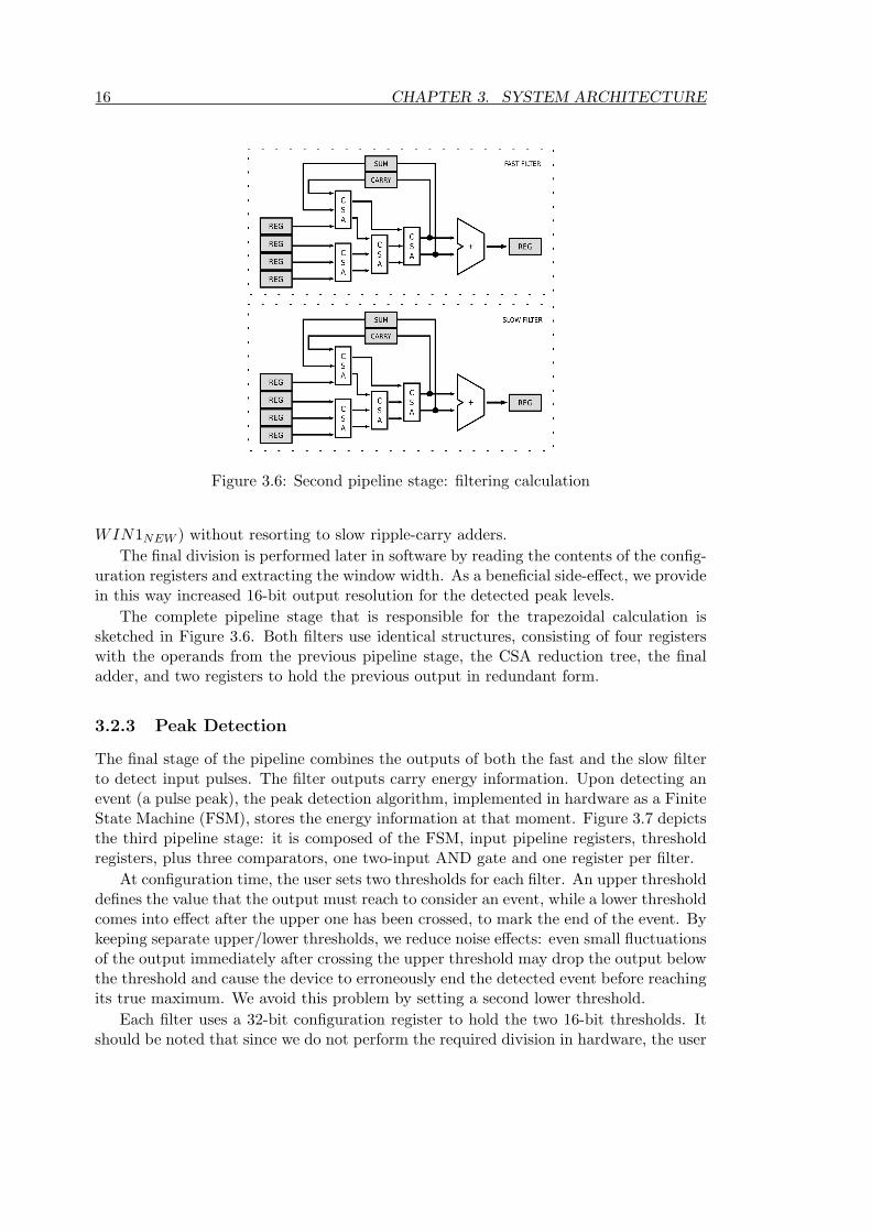
The complete pipeline stage that is responsible for the trapezoidal calculation issketched in Figure 3.6. Both filters use identical structures, consisting of four registerswith the operands from the previous pipeline stage, the CSA reduction tree, the finaladder, and two registers to hold the previous output in redundant form.
3.2.3 Peak Detection
The final stage of the pipeline combines the outputs of both the fast and the slow filterto detect input pulses. The filter outputs carry energy information. Upon detecting anevent (a pulse peak), the peak detection algorithm, implemented in hardware as a FiniteState Machine (FSM), stores the energy information at that moment. Figure 3.7 depictsthe third pipeline stage: it is composed of the FSM, input pipeline registers, thresholdregisters, plus three comparators, one two-input AND gate and one register per filter.
At configuration time, the user sets two thresholds for each filter. An upper thresholddefines the value that the output must reach to consider an event, while a lower thresholdcomes into effect after the upper one has been crossed, to mark the end of the event. Bykeeping separate upper/lower thresholds, we reduce noise effects: even small fluctuationsof the output immediately after crossing the upper threshold may drop the output belowthe threshold and cause the device to erroneously end the detected event before reachingits true maximum. We avoid this problem by setting a second lower threshold.
Each filter uses a 32-bit configuration register to hold the two 16-bit thresholds. Itshould be noted that since we do not perform the required division in hardware, the user

3.2. FILTER DATAPATH 17
Figure 3.7: Third pipeline stage: peak detection
should provide all threshold values multiplied by the window width.During runtime, the outputs of the filters are constantly compared against their two
thresholds. One comparator is used to check whether an output is greater than the upperthreshold, while another comparator is used to check whether the output is smaller thanthe lower threshold. The outputs of both comparators feed into the peak detection FSM.
The concept of using a dual-filter setup was introduced in Section 2.2. Using thecombined four comparator outputs of both filters, we build an FSM that is able to detectclean events and discard pile-ups. Our FSM design is presented in Figure 3.8. Whenidle, the FSM rests at state 0. In case of an event, the first threshold to be crossed is theupper threshold of the fast filter (FF ↑). The output of the corresponding comparatorwill be set to one, triggering the transition to state 1. Depending on the filters setup,the next event will be either from the slow filter crossing the upper threshold (SF ↑) aswell, or from FF ↓, leading to states 3 and 2, respectively. Whichever event happensfirst (SF ↑ or FF ↓), the other one should be the one to follow, in which case the FSMmakes a transition to state 4. To make a complete event (E), the slow filter must returntoo (SF ↓). Any other series of events results in a pile-up (P) and are discarded. In anycase, the FSM always returns to state 0.
To actually detect a peak within an event, we make use of the third comparator inFigure 3.7. A register is used to store the last maximum output value. Every cycle, wecompare the new filter output to the maximum value. If we detect a new maximum andwe are over the upper threshold, we store and output the new value. This way, aftercrossing the upper threshold, the final register keeps track of the maximum value, andwill keep it until a new event has started. When the FSM detects a new event, it signalsto the AMBA block that the output of the filter datapath is valid. The final output ofthe datapath is a 32-bit value combining the 16-bit peaks of both filters.

18 CHAPTER 3. SYSTEM ARCHITECTURE
Figure 3.8: Peak detection finite state machine
3.3 AMBA Control Block
The second half of the pulse detector is the AMBA [9] control block. This block formsthe communication link between the filter datapath and the controlling application thatis running on the embedded on-chip processor.
Our pulse detector is designed to communicate over the AMBA Advanced PeripheralBus (APB). AMBA is a popular interconnection protocol, especially in SoC implemen-tations. APB is a slow single-master non-pipelined bus that is usually attached to afaster AHB bus. The AHB/APB bridge acts like the master and all APB peripheralsare slaves.
In our implementation we can afford a slow bus because we perform real-time calcu-lations and reduce the amount of output data; for every pulse event, only a single 32-bitvalue representing the pulse height is produced. Using APB has several advantages overfaster interconnections like AHB. The simplicity of the protocol reduces the complexityof the interface, resulting in a more compact design with less wires and logic. Further-more, APB is optimised for low power consumption, a much appreciated attribute whendesigning for space applications.
The diagram of the AMBA block can be seen in Figure 3.9. A set of 32-bit con-figuration/status registers appear as a 32-bit aligned memory-mapped region, accessibleover the APB bus. Communication with the device consists of read and write operationsinside this I/O region. Major components inside the block, apart from the registers,include the AMBA signal decoding logic and two FSMs; one is programmed to start,stop, and reconfigure the filter datapath, while the other one is in charge of retrievingthe pulse heights.
The registers are used to store the configuration and to control the filter. Configurableparameters include the window width and gap of the trapezoidal filters, and the peakdetection thresholds. Another register is used to hold the last detected pulse height. For

3.3. AMBA CONTROL BLOCK 19
Figure 3.9: Block diagram of the AMBA interface
(a) Read (b) Write
Figure 3.10: AMBA APB read and write bus cycles
a complete list of the available registers and their purpose, refer to Appendix A.The AMBA APB bus uses a typical set of control and data signals. Figure 3.10
presents the timing diagrams of the read and write bus cycles. Based on this information,we have built a simple decoding mechanism that controls the loading signal to all registersand returns the correct register contents.
Using the AMBA APB bus, the application accesses the configuration registers toset the desired window and gap widths, as well as the thresholds for both filters. Afterchoosing and setting up the desired values, the application then sends a command toreconfigure the filters, which triggers the asynchronous transition of the configurationvalues to the filter datapath. Following that, a command to start the computation

20 CHAPTER 3. SYSTEM ARCHITECTURE
(a) Filter control FSM (b) Pulse retrieval FSM
Figure 3.11: States and transitions of the AMBA control block
enables the processing of incoming samples, while a command to stop terminates theprocess.
Figure 3.11 presents the available states and transitions of both FSMs. Upon reset,the system enters the “reset” state for a short period of time, before moving to the “idle”state. From there, a command from the user to start processing will move the systemto the “running” state, while a command to reconfigure will move the system to the“reconfiguration” state (until the new setup is loaded and the system returns to idlestate). While running, a user command to stop will return the system to the idle state,while a reconfiguration command will move again the system to the “reconfiguration”state. If upon completion of the reconfiguration step the system is still in operationalmode (in other words, the START bit of the configuration/status register is still ‘1’),then the filters will resume operation (after a quick transition through the “idle” state),otherwise the system will rest in the “idle” state. This corresponds to the filter controlFSM illustrated in Figure 3.11a.
The second FSM (Figure 3.11b) is programmed to communicate with the filter dat-apath block and retrieve the pulse heights. If a “valid” signal is received from the filterdatapath while the device is running, the second FSM moves to the next state and loadsthe new value in the result register. It then issues a signal to acknowledge the receptionand waits for the valid signal to be deasserted before returning to the idle state.
3.4 Multiple Clock Domains
Very often in the design of embedded systems that interact with the environment, thecircumstances dictate the use of multiple clocks. Data acquisition blocks may need tosample a natural event at a high rate to ensure the required resolution. This rate is oftenmuch higher than the one we can achieve and/or want for the rest of our design.
In our case, another important argument in favour of using multiple clocks is thatwe design a modular IP core. Our module can be interfaced to a number of SoC solu-

3.4. MULTIPLE CLOCK DOMAINS 21
Figure 3.12: Four-phase handshaking protocol
tions, and the complete design can be programmed in a variety of silicon chips. Thesefacts introduce uncertainty concerning the clock rate of the complete system. However,we would like our pulse detector to function with a predefined speed and resolution,decoupled from the performance of the supporting system.
Multiple clock domains is the solution to the above-stated problems, but not withoutpitfalls. When designing using multiple clocks with different frequencies and/or phases,one must pay special attention to minimise the number of signals which cross clockdomains, and to properly synchronise those that do so.
Synchronisation is needed to avoid metastability issues [26]. If not properly synchro-nised, a signal has the chance to violate setup and hold times on the receiving memoryelement, and arrive at exactly the wrong moment to trigger a metastable state for anunknown length of time.
Several solutions are available for reducing the risk of metastability, with varyingdegrees of protection. For the first version of our design we chose to implement thesimplest of those: we place a pair of flip-flops in series on the receiving side of everysignal that crosses clock domains. By doing so, we greatly reduce the chance of ametastable signal reaching the receiving logic.
However, duplicating flip-flops increases the area footprint and introduces latency.Therefore, we must keep the number of signals which cross clock domains to a bareminimum. Furthermore, for multi-bit signals, it is not efficient to duplicate flip-flops forevery single bit. The solution is to add two handshaking lines to properly synchronise thedelivery of the multi-bit value. Of course, the signals of the handshaking lines themselvesshould be protected from metastability, but this introduces only two more flip-flops. Forour handshake mechanism we use the four-phase protocol depicted in Figure 3.12.
The complete set of cross-clock domain signals is illustrated in Figure 3.13. Grayboxes represent metastability protection flip-flops. A reset and a start signal cross theclock domains to allow us to control the filter datapath from the control block side. Bothof them correspond to bits in the configuration/status register (refer to Appendix A.1).Two sets of four-phase handshaking lines protect the configuration and result buses,both 32-bits wide. The configuration bus is used to transfer the configuration values tothe filter datapath, while the result bus transfers the detected peaks back to the controlblock.

22 CHAPTER 3. SYSTEM ARCHITECTURE
Figure 3.13: Set of cross-clock domain signals

Experimental Setup & Results 4In the previous chapters we argued in favour of a System-On-Chip approach to digitalpulse detection and discussed the system architecture of the proposed IP core. In thischapter we present the experimental setup that was used to develop and test the func-tionality of our module within a complete, self-sustained single-chip system. We alsopresented the preliminary results that we obtained using this setup.
In the following sections, we examine the library of IP cores that was used to assembleour SoC, including the on-chip processor, interconnection bus, and interface to host PC(Section 4.1). We also look into the embedded C code that we wrote to control theentire process. In Section 4.2 we present the development board and FPGA used toprogram our design, together with a custom mezzanine board that hosts the analogreadout electronics, up to and including the ADCs. The mezzanine board is used todigitise the input signal, and in Section 4.3 we briefly discuss our setup for generatingand capturing radiation-induced pulses. Section 4.4 contains a review of the tools thatwere used to develop, simulate, synthesise, debug, and process the results. The obtainedresults are presented in the last part of this chapter, in Section 4.5.
4.1 GRLIB IP Core Library
The GRLIB IP library of reusable cores is centered around the AMBA on-chip inter-connect bus. The library is developed and maintained by Gaisler Research [1]. It isprovided under the GNU GPL open-source license and it is largely vendor independent.Our FPGA-agnostic IP core, combined with a selection of IP cores from GRLIB, can beprogrammed in almost any FPGA available on the market, provided that it fits insidethe target chip.
GRLIB uses the AMBA AHB as its main interconnect, with an optional AHB/APBbridge to connect a slave APB bus. The library includes cores for the LEON3 gen-eral purpose processor, 32-bit PC133 SDRAM controller, 32-bit PCI bridge with DMA,10/100 Mbit ethernet MAC, 8/16/32-bit PROM and SRAM controller, CAN controller,TAP controller, UART with FIFO, modular timer unit, interrupt controller, and a 32-bitGPIO port. Memory and pad generators are available for Virage, Xilinx, UMC, Atmel,Altera, Actel, and Lattice.
In our SoC implementation, apart from our own pulse detector core, we also makeuse of the LEON3 processor, AHB bus controller, memory controller, a debug supportunit for the LEON3 over a serial port, and the AHB/APB bridge. On the APB bus, weconnect another UART port, the interrupt controller, and our core. The block diagramof the complete SoC can be seen in Figure 4.1.
23

24 CHAPTER 4. EXPERIMENTAL SETUP & RESULTS
Figure 4.1: Complete System-On-Chip block diagram
4.1.1 The LEON3 Processor
The LEON3 is a synthesisable VHDL model of a 32-bit processor compliant with theSPARC V8 architecture. It is a Symmetric Multi-Processing (SMP) capable CPU, with a7-stage pipeline and hardware MUL, MAC, and DIV units. It also supports an additionalIEEE-754 FPU. According to the manufacturer, the processor can reach up to 125 MHzon an FPGA, or 400 MHz on a 0.13 um ASIC technology.
The LEON3 follows the “Harvard architecture”, using a single main memory butseparate instruction and data caches. Caches are configurable as either direct-mappedor 2- to 4-way set associative, with 256 KB per set. Supported replacement strategiesinclude random, least-recently used (LRU), and least-recently replaced (LRR, also knownas FIFO).
In our system, the processor has a complementary role, mostly control of the entirepulse detection process, since the majority of the calculations are performed by ourdedicated hardware. Hence we would like to use a minimal instance of the processor.To this end, we configured the LEON3 with a single CPU, direct-mapped (1-way setassociative) instruction and data caches, and no hardware floating-point support. We dohowever keep the DIV unit, in order to quickly perform the final division of detected pulseheights (see also Section 3.2 on page 10). To facilitate debugging, we’ve also includedthe non-intrusive Debug Support Unit (DSU), that offers access via the serial port to allon-chip registers and memory, together with trace buffers of both executed instructionsand AMBA bus traffic.
LEON3 is also available in a non-free fault-tolerant (FT) version that offers SingleEvent Upset (SEU) immunity with no timing penalty compared to the non-FT version.This fact makes the LEON3 a very attractive solution for space-oriented SoC designs.
4.1.2 Plug & Play Capability
All GRLIB cores use the same data structures to declare the AMBA interfaces, and caneasily be connected together. Figure 4.1.2 lists the available APB input/output sets ofsignals, while Figure 4.1.2 presents an example of a typical declaration of an APB slavedevice using these records.

4.1. GRLIB IP CORE LIBRARY 25
−− APB s l a v e inpu t stype apb s l v i n t yp e i s record
p s e l : s t d l o g i c v e c t o r (0 to NAPBSLV−1); −− s l a v e s e l e c tpenable : s t d u l o g i c ; −− s t r o b epaddr : s t d l o g i c v e c t o r (31 downto 0 ) ; −− address bus ( by te )pwrite : s t d u l o g i c ; −− wr i t epwdata : s t d l o g i c v e c t o r (31 downto 0 ) ; −− wr i t e data busp i rq : s t d l o g i c v e c t o r (NAHBIRQ−1 downto 0 ) ; −− i n t e r r up t r e s u l t bus
end record ;
−− APB s l a v e output stype apb s l v ou t type i s record
prdata : s t d l o g i c v e c t o r (31 downto 0 ) ; −− read data busp i rq : s t d l o g i c v e c t o r (NAHBIRQ−1 downto 0 ) ; −− i n t e r r up t buspcon f i g : apb con f i g type ; −− memory access reg .pindex : i n t e g e r range 0 to NAPBSLV −1; −− diag use only
end record ;
Figure 4.2: GRLIB APB slave input/output records
l ibrary g r l i b ;use g r l i b . amba . a l l ;
l ibrary i e e e ;use i e e e . s t d l o g i c . a l l ;
entity apbs lave i sgeneric (
pindex : i n t e g e r := 0 ;paddr : i n t e g e r := 0 ;pmask : i n t e g e r := 0 ;p i rq : i n t e g e r := 0 ;imask : i n t e g e r := 0 ) ;
port (r s t : in s t d u l o g i c ;c l k : in s t d u l o g i c ;apbi : in apb s l v i n t yp e ; −− APB s l a v e inpu t sapbo : out apb s l v ou t type −− APB s l a v e output s
) ;end entity ;
Figure 4.3: Typical GRLIB APB slave entity definition
The pconfig field in the output record of Figure 4.1.2 adds “plug & play” capability tothe AMBA APB bus. It includes information like vendor and device ID, address mappinginformation and assigned irq line. This information is forwarded to the APB bus master(the AHB/APB bridge), so that it can be later retrieved by the controlling application(or operating system) to automatically configure itself to “talk” to the hardware.
4.1.3 PC Interface
The complete SoC interfaces via the serial port to a host PC. During normal operation,the pulse detector captures the heights of the detected pulse events and transfers themto the LEON3 processor. Software running on processor assembles a histogram (number

26 CHAPTER 4. EXPERIMENTAL SETUP & RESULTS
of detected events per pulse height unit) out of the received values and transmits it tothe host PC for further processing and visualisation.
Communicating over the serial port is a simple task: the system is configured toredirect all output to the serial port, so transmission is as simple as printing values on“screen”. On the host PC side, a terminal application with logging capabilities is all thatis needed to receive the transmitted values. Appendix B contains example embedded Ccode, showing how to transmit results to the host PC.
Future versions of our system will drop the serial interface in favour of SpaceWire(SpW) [16]. The European Space Agency offers ready to use SpaceWire cores, and thereis even an SpW core with an AMBA interface. Thanks to the SoC approach, adding anew core that already supports our interconnect should be a trivial job.
4.2 Development Board
The complete design (LEON3, AMBA bus, peripherals, and digital pulse detector) wasprogrammed on a Xilinx FPGA, which was hosted by the GR-XC3S development boardby Pender Electronics GmbH [5]. The GR-XC3S is a 15x9.5cm low-cost developmentboard that was designed with the LEON3/GRLIB system in mind.
Figure 4.4 presents a top view of the GR-XC3S board. The FPGA is a 1.5 milliongate XC3S1500 Spartan3 from Xilinx [27]. Just below the FPGA chip, one can find theon-board 64MB SDRAM memory, as well as the 8MB flash memory. On the top left,we can also see the two serial ports, one for the Debug Support Unit, and another onefor interfacing to the host PC. The existing 20-pin headers were used to interface to theanalogue electronics mezzanine board (see below, Section 4.2.1). The FPGA is clockedby a 50MHz crystal that is part of the development board.
Aside from the parts already mentioned, the board also contains an Ethernet MACand PHY, 24-bit video DAC, USB PHY controller, and PS2 mouse and keyboard inter-faces. These components were not used in our system. By removing them (and theirrespective connectors) we can arrive to a very small and effective solution.
4.2.1 The Mezzanine Board
Although not part of this research, the analogue electronics that deliver data to ourdigital pulse detector are very important to the quality of the result. Cosine ResearchBV kindly offered a custom-built mezzanine board which we can easily plug into ourdevelopment board. Figure 4.5 presents the development board with the mezzanineplugged in.
The mezzanine hosts analogue signal conditioning circuits and the Analog-to-Digitalconverter. The ADC is 8-bit wide, and can be operated at 100MHz maximum. Theboard also includes two DACs, also 8-bit, 100MHz. The DACs are used to reconstructthe input and outputs of the system, for debugging purposes. The mezzanine expectsto receive its clock from the development board. Distributing the clock to the system isour next topic.

4.2. DEVELOPMENT BOARD 27
Figure 4.4: Top view of the development board
Figure 4.5: Development board with fitted mezzanine
4.2.2 Clock Distribution
The complete system needs a diverse set of clock frequencies. The LEON3 processorand AMBA bus can be safely clocked at 40MHz using the XC3S1500 Spartan3 FPGA.The external SDRAM memory also needs the same 40MHz clock. The mezzanine board

28 CHAPTER 4. EXPERIMENTAL SETUP & RESULTS
Figure 4.6: Clock distribution network
requires a 100MHz clock, and our pulse detector requires both the 40MHz clock for theAMBA block and the 100MHz for the filter datapath.
All required clocks are generated inside the FPGA from the 50MHz input clock signal,using the embedded Digital Clock Managers (DCM) of the chip [28]. This particularFPGA has four DCMs, placed on the four corners of the chip. Figure 4.6 illustrateshow we make use of these four DCMs to synthesise all the required clock signals fromthe main 50MHz board clock (represented by the red line). The two bottom DCMsare instantiated by GRLIB to generate the 40MHz internal system clock (green lines)and the external clock to the SDRAM memory. The two DCMs on the top provide the100MHz clock to the filter datapath block of our design (blue lines) and the externalclock to the mezzanine board. Both external clocks make use of the Delay-Locked-Loop(DLL) mechanism of the DCM which automatically adjusts the phase of the generatedclock to take into account for clock skew.
4.3 Pulse Generation
Our experimental setup would not be complete without a source of pulses. This sourcewas again provided by cosine Research BV. The pulse events were generated by a Cobalt-60 source and captured by a scintillator LaBr3 cylinder, coupled to a Hamamatsu R6231photomultiplier tube with a pre-amplifier. This kind of source emits approximately 6000γ-rays per second, one third of which is captured by the scintillator and converted to

4.4. DEVELOPMENT TOOLS 29
light. The emitted light is then converted to electrical current and is amplified beforeentering the digitisation circuit on the mezzanine board. Such a pulse event has a risetime of 500ns and fall time in the order of 100us.
4.4 Development Tools
Another important aspect of this project is the set of tools that we used for developmentand testing. We decided that all selected software tools should be available for free andif possible open-source. As a starting point, a 32-bit x86 GNU/Linux laptop was used asthe main development platform, and GNU/Emacs was the default VHDL and C editorthroughout the project.
For the needs of simulating the VHDL code, we selected GHDL [2]. GHDL usesGCC and conforms fully with the IEEE VHDL standards. GHDL creates testbenchexecutable files and can output to Value Change Dump (VCD) ascii file format, as wellas its own GHW compressed ascii file format. The GHW format is preferable for long-length simulations because it greatly reduces the output file size. The resulting file wasvisualized using GTKWave [4], a free wave viewer with the ability to read GHW andVCD files (among many others). Both GHDL and GTKWave are open-source software,released under the GPL.
In order to synthesize the complete SoC and transfer the bitstream to the FPGA,we used the scripts provided by GRLIB. These scripts internally use the command-lineXilinx synthesis and place/route tools. For this purpose, we downloaded and used theISE WebPack from the Xilinx website. The ISE WebPack is free but not open-source.Apart from the standard tools already mentioned, the WebPack also includes a varietyof tools that proved to be very useful: the FPGA editor is a tool that visualises theplacement and routing of the synthesised system, and helped us debug problems withvery long paths. Figures 4.6 and 4.8, on pages 28 and 31 respectively, where createdusing the FPGA editor. Another tool that is part of the WebPack, the timing analyser,was also very important for debugging, because it reported all paths which failed thetiming constraints and was able to highlight them on the FPGA editor tool.
For the embedded C code, we used the BCC LEON3 cross-compiler from GaislerResearch. BCC is a complete cross-compilation toolchain for the LEON3 processor. Itis based on GCC3 and includes the Newlib Embedded C library. Gaisler Research alsooffers a small tool to pack the compiled executable into a PROM file that we can uploadto the on-board flash memory.
Uploading the PROM file or directly accessing the memory of the system is accom-plished with GRMON, a debug monitor for the LEON3 processor that uses the Digi-tal Support Unit. GRMON allows access to all registers and memory, instruction andAMBA transaction trace buffers, downloading and execution of applications, breakpointinsertion, remote connection to GDB and flash programming. GRMON is not free, butthere is an evaluation version. All tools mentioned from Gaisler Research are availableat the company’s website [1].
On the host PC side, we received the results via the serial port and captured themusing a standard open-source terminal application. We stored the data in a text file andvisualized it using Gnuplot [3], an established open-source data plotting software.

30 CHAPTER 4. EXPERIMENTAL SETUP & RESULTS
4.5 Results
In this section we present the results from the experimental setup that we described in theprevious sections. These results are preliminary and only serve to verify the correctnessof the design. A complete characterisation of the device requires further testing, butfalls outside the scope of this master thesis project.
4.5.1 Area
We first look into the hardware resources. We have already mentioned that we used aXilinx XC3S1500 FPGA. Figure 4.5.1 lists the usage of the FPGA resources, taken fromthe reports of the Xilinx tools. We can see that we are using 73% of the available slicesfor our SoC. This report however does not offer any insight on the resource usage of theindividual SoC modules.
In order to have a more in-depth view of the allocated resources, we use the FPGAeditor tool from Xilinx and colour the nets of various parts of our design. Figure 4.8apresents the basic output of the FPGA editor tool, corresponding to the 73% usage of thechip. In Figure 4.8b we can see how the resources are divided between GRLIB (white)and our IP core (blue for the datapath, red for the amba block). A more detailed viewof the GRLIB area is given in Figure 4.8c, where we see that the LEON3 processor takesmost of the space, followed by the Debug Support Unit.
Noticing the large amount of resources needed for the filter datapath of our design, wetried to provide an explanation. If we compare Figure 4.8d to 4.8b, we can see that themain problem behind the increased area usage is the existence of the 256:1 multiplexers.This was foreseen and discussed already in Section 3.2.1, where we also argued in favourof our choice, mainly because one of the requirements was to keep the design FPGA-agnostic, a fact that ruled out the use of dynamic run-time reconfiguration. Since ourSoC fits the FPGA and the timing constraints, there is no reason to change our design.However, should it be needed, we can always replace the 256:1 multiplexers with 64:1versions. This would save a lot of resources, but on the downside, it would allow theuser to choose only one position in every four samples, thus reducing the resolution ofthe filter parameters from 10ns steps (with a 100MHz clock) to 40ns steps.
4.5.2 Performance
Regarding the performance of our system, the initial requirements stated that the SoCshould work at the same frequency that it worked without our modifications (40MHz),while the filtering and peak detection should ideally match the speed of the ADC(100MHz). Figure 4.5.2 presents the relevant part from the timing report of the Xil-inx tools. It is clear that our design has managed to reach the given targets.
However, it is not equally clear whether our design could actually go faster, since theabove requirements were given to the tools as timing constraints, and the tools terminatetheir “exploration” of available solutions as soon as they find something that satisfiesthe given requirements. We do know that an early version of the filter datapath alone,without GRLIB, the AMBA control block or assignment of signals to input/output pinsof the FPGA, could reach speeds above 300MHz, almost touching the limit of the FPGA

4.5. RESULTS 31
Logic U t i l i z a t i o n :Number o f S l i c e F l ip Flops : 5 ,048 out o f 26 ,624 18%Number o f 4 input LUTs : 15 ,898 out o f 26 ,624 59%
Logic D i s t r i bu t i on :Number o f occupied S l i c e s : 9 ,744 out o f 13 ,312 73%
Total Number o f 4 input LUTs : 16 ,104 out o f 26 ,624 60%Number used as l o g i c : 15 ,898Number used as a route−thru : 131Number used as Sh i f t r e g i s t e r s : 43Number o f bonded IOBs : 125 out o f 333 37%
IOB Fl ip Flops : 45Number o f Block RAMs: 18 out o f 32 56%Number o f MULT18X18s : 1 out o f 32 3%Number o f GCLKs: 3 out o f 8 37%Number o f DCMs: 4 out o f 4 100%
Total equ iva l en t gate count f o r des ign : 1 ,373 ,808Addi t iona l JTAG gate count f o r IOBs : 6 ,000
Figure 4.7: Post-Map FPGA resource utilisation
(a) (b)
(c) (d)
Figure 4.8: XC3S1500 Spartan3 FPGA resource usage
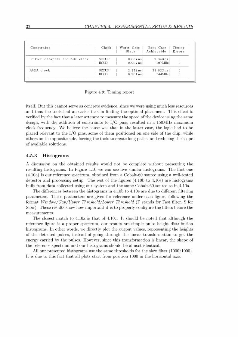
32 CHAPTER 4. EXPERIMENTAL SETUP & RESULTS
−−−−−−−−−−−−−−−−−−−−−−−−−−−−−−−−−−−−−−−−−−−−−−−−−−−−−−−−−−−−−−−−−−−−−−−−−−−−−−−−Constra int | Check | Worst Case | Best Case | Timing
| | Slack | Achievable | Errors−−−−−−−−−−−−−−−−−−−−−−−−−−−−−−−−−−−−−−−−−−−−−−−−−−−−−−−−−−−−−−−−−−−−−−−−−−−−−−−−
F i l t e r datapath and ADC c lock | SETUP | 0 .657 ns | 9 .343 ns | 0| HOLD | 0 .907 ns | ˜107MHz | 0
−−−−−−−−−−−−−−−−−−−−−−−−−−−−−−−−−−−−−−−−−−−−−−−−−−−−−−−−−−−−−−−−−−−−−−−−−−−−−−−−AMBA c lock | SETUP | 2 .378 ns | 22 .622 ns | 0
| HOLD | 0 .901 ns | ˜44MHz | 0−−−−−−−−−−−−−−−−−−−−−−−−−−−−−−−−−−−−−−−−−−−−−−−−−−−−−−−−−−−−−−−−−−−−−−−−−−−−−−−−
Figure 4.9: Timing report
itself. But this cannot serve as concrete evidence, since we were using much less resourcesand thus the tools had an easier task in finding the optimal placement. This effect isverified by the fact that a later attempt to measure the speed of the device using the samedesign, with the addition of constraints to I/O pins, resulted in a 150MHz maximumclock frequency. We believe the cause was that in the latter case, the logic had to beplaced relevant to the I/O pins, some of them positioned on one side of the chip, whileothers on the opposite side, forcing the tools to create long paths, and reducing the scopeof available solutions.
4.5.3 Histograms
A discussion on the obtained results would not be complete without presenting theresulting histograms. In Figure 4.10 we can see five similar histograms. The first one(4.10a) is our reference spectrum, obtained from a Cobalt-60 source using a well-testeddetector and processing setup. The rest of the figures (4.10b to 4.10e) are histogramsbuilt from data collected using our system and the same Cobalt-60 source as in 4.10a.
The differences between the histograms in 4.10b to 4.10e are due to different filteringparameters. These parameters are given for reference under each figure, following theformat Window/Gap/Upper Threshold/Lower Threshold (F stands for Fast filter, S forSlow). These results show how important it is to properly configure the filters before themeasurements.
The closest match to 4.10a is that of 4.10c. It should be noted that although thereference figure is a proper spectrum, our results are simple pulse height distributionhistograms. In other words, we directly plot the output values, representing the heightsof the detected pulses, instead of going through the linear transformation to get theenergy carried by the pulses. However, since this transformation is linear, the shape ofthe reference spectrum and our histograms should be almost identical.
All our presented histograms use the same thresholds for the slow filter (1000/1000).It is due to this fact that all plots start from position 1000 in the horizontal axis.
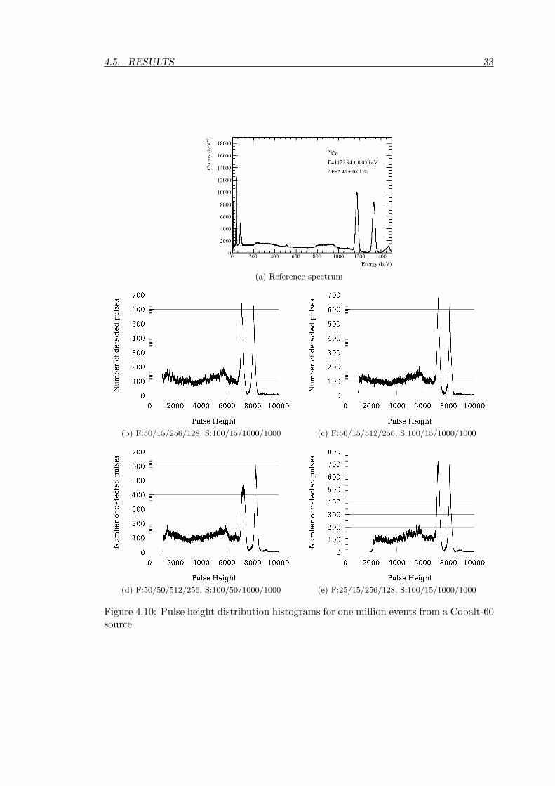
4.5. RESULTS 33
(a) Reference spectrum
(b) F:50/15/256/128, S:100/15/1000/1000 (c) F:50/15/512/256, S:100/15/1000/1000
(d) F:50/50/512/256, S:100/50/1000/1000 (e) F:25/15/256/128, S:100/15/1000/1000
Figure 4.10: Pulse height distribution histograms for one million events from a Cobalt-60source
Conclusion 5In this thesis we described the principles, the design, and the implementation of a fully-configurable digital pulse detector. We studied existing methods for digital pulse shaping,height analysis, and pile-up rejection. We proposed a high throughput, low latency serialcomputation of the trapezoidal shaping function, using a dual filter setup and a customalgorithm for peak detection. We arranged the complete filter datapath in a three stagepipeline to further increase the performance of the system. We encapsulated the pulsedetector into an AMBA IP core, and combined it with an on-chip processor, to arriveat a single-chip SoC solution. We created a small, lightweight device, for real-time, zerodead-time radiation monitoring and gamma-ray spectroscopy, keeping in mind the needsof current and future space exploration missions. The ability to run additional softwareon the embedded on-chip processor of the SoC adds to the flexibility and reusability ofthe design.
Although we chose to develop a digital pulse detector as a representative exampleof electronic instrumentation in space applications, our methodology is applicable tomany other cases as well. Indeed, as the capacity of FPGAs increases, it is not hardto imagine a multitude of electronic instruments embedded within a single chip, underthe same interconnection bus and the control of one or more on-chip processors. Therecent introduction of mixed-signal FPGAs with embedded analog electronics takes thesingle-chip idea even further: such FPGAs embed the ADCs into the chip, and offerhigh-voltage tolerant analog inputs, effectively eliminating the need for external analogcircuits.
Another recent trend in space electronics is the study of Micro-Electro-MechanicalSystems (MEMS) to further reduce the size of payloads. MEMS components integratemechanical elements, sensors, actuators, and electronics in a single silicon chip. To-gether with mixed-signal FPGAs and Systems-on-Chip, MEMS technology completesthe picture of, perhaps tomorrow’s, truly single-chip highly-integrated payloads.
We believe our work is important because it highlights the potential benefits inthe use of reconfigurable hardware in future space missions; by compacting multiplefunctions inside a complete SoC design, higher levels of integration can be achieved, whileincreasing the re-usability of the design and decreasing development time, effectivelyreducing the overall cost of the mission.
We conclude our discussion in the following sections with some final words on theproblems that we encountered (Section 5.1), lessons learned (Section 5.2), and possibledirections for future research on the subject (Section 5.3).
34

5.1. PROBLEMS ENCOUNTERED 35
5.1 Problems Encountered
One of the most persisting problems throughout the various phases of the developmentprocess was to maintain the design FPGA-agnostic. Even if the developer strives to pro-vide a clean, generic VHDL source code, he cannot avoid the addition of manufacturer-specific macros at the low level description of the system. A typical example is that ofthe embedded clock managers (detailed in Section 4.2.2) on the Xilinx Spartan3 FPGA.These DCMs play a vital role in generating the required clock signals for the variousparts of our system. However, not all FPGAs provide such facilities, and even whenthey do, their instantiation might have to be done in a different way. The existence ofthe DCMS is unavoidable in this case, but they effectively “tie” our design to the specificFPGA family.
GRLIB, the IP core library of our prototype, deals with this problem by providinggeneric configurable instantiation blocks, together with a lower set of libraries for differentFPGAs and development boards. This approach solves the issue, but requires constantupdating of the low level libraries to support newer FPGAs. The only true solution tothe problem would be a standardisation process, where different manufacturers wouldagree on a common way of providing the underlying resources. This process would alsoenable for portable, dynamically-reconfigurable designs, giving complete freedom to thedeveloper to choose his/her hardware and tools, based on the requirements of the targetsystem. By not having to go over a learning curve when switching FPGA models, and re-using existing libraries, one can also reduce the development time, and build on his/herprevious knowledge to produce better designs every time.
Another cause for “tainting” the code with non-generic expressions is the currentconfusion when it comes to standard VHDL libraries. VHDL is defined by IEEE, to-gether with a set of standard libraries, namely the packages “std logic 1164” defined byIEEE 1164, “numeric bit” and “numeric std” defined by IEEE 1076.3, and “vital timing”and “vital primitives” defined by IEEE 1076.4. However, there exist other popularadditions to the IEEE library, like the packages “std logic arith”, “std logic signed”,“std logic unsigned”, and “std logic textio”, that have been added without permissionfrom IEEE and are not part of the standard. The definitions of symbols and operatorsbetween the different packages overlap, and can cause very obscure and hard to find bugsin the resulting design. When combining different cores, one should pay attention to theIEEE libraries used in each core.
Adding IP cores to existing libraries, or combining cores from different sources, is nota trouble-free process either. Apart from the problem of interfacing the different signaltypes (e.g. std logic vectors versus signed/unsigned, or bit vectors), once too often thedeveloper has to go deep into the code of cores that he/she has not written, to trackdown compatibility problems. The automated tools that usually accompany a library,work with the predefined set of building blocks, but require modifications to includeexternal cores, leading to increased development cycles.
An equally important issue is that of debugging the resulting system. It is commonpractice to develop code for FPGAs with less attention to detail and proper designprocedures, because there is always the possibility to reprogram the device. However,a bug in a modern SoC, within a medium-sized FPGA, can be very difficult to trace

36 CHAPTER 5. CONCLUSION
and fix. As newer FPGAs offer greater capacities, the problem will only become worse.The proper tools can be invaluable in dealing with bugs, but the process can be verytime-consuming. It is better to think of debugging during the initial steps of the design.We further discuss solutions for debugging in Section 5.3.
During the last steps of the development of our experimental system, when most ofthe components were in place, we noticed that it would take over 45 minutes to produce asingle new version of the system, including synthesis, mapping, placement, and routing.This imposes an upper limit to the number of different alternatives one can try everyday. In practice, if we also take into consideration the time that it takes to implementthe changes and test the system, one cannot usually attempt more than two or threealternatives per day. The long waiting times also make the developer more impatientand prone to errors.
We have already mentioned the use of DCMs to provide the necessary clock signals tothe FPGA and external analog circuits. Another problem related to the clock network isthat of calculating and balancing the clock skew, particularly when it comes to externalcircuits. In our system, a 100MHz clock signal was provided by a single DCM to theexternal ADC, but also to some DACs that reconstructed the digital filter outputs forinspection on the oscilloscope. The ADC is “before” the FPGA, and thus requires theclock signal to have some negative skew to accommodate for the transmission delay, whilethe DACs are “after” the FPGA, and require the clock signal to have some positive skew.The DCM has only one output and a single skew adjustment. The solution is to placetime constraints on the pins of the FPGA connected to the ADC and DACs, but theprocess of manually determining the correct skew is also time-consuming.
5.2 Lessons Learned
It seems there is never “enough” when it comes to careful thinking and planning of acomplex project. Many times did we rush into implementing a new idea, only to findourselves later spending long hours into trying to debug the problems. Nevertheless, theoverall approach was organised and managed, and the result was indeed a functionaldigital pulse detector.
Performing simulations at every step of the development process, even when we ex-pect to see the obvious, can be a very rewarding habit. We discovered that it is moretime-efficient to create our own VHDL testbench files for every entity in a hierarchicalway, and manage the execution of the testbenches within scripts. Establishing an auto-mated simulation process from the early development steps, is also a good motive to runthe simulations more often.
Another important lesson was on the use of timing and placement constraints. Adesign may exist as an idea within the lines of VHDL code, but it is the use of constraintsthat makes it possible to create a functional, real device. In our example, a synthesistool would never succeed in achieving a 10ns clock period with the critical path passingthrough the 256:1 multiplexers, without the extra information that the select signals ofthe multiplexers are actually static.
In another case, regarding placement constraints this time, the orientation of thefour DCMs on the corners of the chip greatly affects the overall arrangement, and thus

5.3. FURTHER WORK 37
the performance of the system, since the GRLIB AMBA IP cores will always be placedby the tools close to the 40MHz DCM, while our IP core will be closer to the 100MHzDCMs. The physical placement of the ADC, DACs and external SDRAM memory alsoaffect our choice of arranging the DCMs.
Our approach to the development was a hardware/software co-design one. The basicidea behind our partitioning of the available functionality into hardware and softwareblocks, was that the hardware should provide the device mechanisms, while the softwareshould dictate the policy of accessing these mechanisms. This kind of approach is alsovery rewarding in the long run, because it allows to use the hardware in ways that werenot imagined during the initial planning.
Last but not least, our approach involved a development toolchain that was free and,in most of the cases, open-source. Throughout the project we gained experience in theuse of these tools, and our result is proof of the fact that today it is possible to designand build prototypes of complex systems without investing a fortune in software licences.
5.3 Further Work
The outcome of our work was a functional digital pulse detector prototype. The obtainedresults using our prototype are very promising but there is always room for improvement.
For future work, the first issues to address would involve improving the hardwaremechanisms. The current way of delivering results to the on-chip processor is rather“weak”, with only a single 32-bit register available for intermediate storage. If the on-chip processor fails to read back fast enough, valuable results will be dropped. In a moremature approach, a dual-clock FIFO could be placed in between the two clock domains ofour design, with the filter datapath producing results, and the AMBA block consumingthem. To further improve the efficiency of the read-back process, an interrupt could begenerated to signal the arrival of new data to the on-chip processor, eliminating the needfor polling, and reducing the traffic over the shared interconnection bus.
An interesting addition to the available hardware mechanisms would be a form ofboundary scan to ease the process of debugging. For this to happen, we need to connectall the registers of the pulse detector into a long chain and provide a serial output,together with a signal to select between normal and scan operation. We can then pausethe execution of the datapath’s pipeline at will, switch to scan mode, and examine thecontents of all registers with the help of a logic analyser, or even transfer the contentsback to the embedded software and out of the system, through the UART port.
In terms of software improvements, our system still needs a calibration mechanism,one that will allow the user to quickly determine the proper filtering parameters (windowwidths, gap widths, and thresholds) for the application at hand. Another improvementwould be to offer to possibility to acquire a histogram without any source of events, andsubtract it later from the real measurements, to accommodate for background noise.Other software improvements concern the ease-of-use of the control application.
Yet another direction for further work involves the complete system instead of thedeveloped IP core only. In the future, we would like to add more modules to the SoC,ones that complement the existing functionality, as well as others for completely different

38 CHAPTER 5. CONCLUSION
scientific measurements, in order to evaluate the performance and needs of such a multi-functional system. Of course, we would have to use a larger FPGA for this purpose.
One module that we would like in particular to add to our SoC is that of aSpaceWire [16] port. SpaceWire is the new interconnection standard for cables and PCBtracks in space applications. It is essentially a revised version of the popular FireWireprotocol, with minor improvements and radiation-hardened manufacturing. The Euro-pean Space Agency provides a SpaceWire port IP core with an AMBA interface, whichwe can easily interface to our existing system, as a drop-in replacement for the UARTport. SpaceWire will offer a high-bandwidth link (up to 400 Mbps), permitting multipleon-chip instruments to communicate with the main spacecraft computer at a high rate.Because of our managed SoC approach, we can replace the UART communication port ofthe system with a SpaceWire one, without any modifications in the rest of the hardware,and only update the running software.
Finally, instead of integrating more modules on-chip, another research initiative couldlook further into the usage of MEMS technology and mixed-signal FGPAs, to create trulysingle-chip instruments, with embedded sensors and analog circuits, placed side by sidewith the digital SoC on the same silicon substrate.
It is a safe bet to predict that in the future the capacity of new FPGAs will continueto grow. Therefore, the real question is not whether we can fit our existing designs intoa given FPGA, but how to effectively use the ever-increasing available resources in theupcoming years, without having to undergo through increased development times. Wehope that the ideas and facts presented in this text will serve as a good starting pointfor future, more complex, miniaturised systems.

Bibliography
[1] Gaisler Research LEON3 synthesizable processor and GRLIB portable IP library,[Online]. Available: http://www.gaisler.com.
[2] GHDL, a complete VHDL simulator, [Online]. Available: http://ghdl.free.fr/.
[3] Gnuplot, a command-line driven interactive data and function plotting utility, [On-line]. Available: http://www.gnuplot.info/.
[4] GTKWave,a fully featured GTK+ based wave viewer, [Online]. Available: http://home.nc.rr.com/gtkwave/.
[5] PENDER Electronic Design GmbH, [Online]. Available: http://www.pender.ch.
[6] The SPARC Architecture Manual Version 8, [Online]. Available: http://www.sparc.org/standards/V8.pdf.
[7] Suitability of reprogrammable FPGAs in space applications, Feasability report nFPGA-002-01, Gaisler Research (2002).
[8] R. Abbiati, A. Geraci, and G. Ripamonti, Self-configuring digital processor for on-line pulse analysis, IEEE Transactions on Nuclear Science 51 (2004), no. 3 Part 3,826–830.
[9] ARM limited, AMBA specification, IHI 0011A, 2.0 ed., 1999.
[10] M. Bautista-Palacios et al., Configurable hardware/software architecture for dataacquisition implementation on FPGA, International Conference on Field Pro-grammable Logic and Applications (2005), 241–246.
[11] M. Bolic and V. Drndarevic, Digital gamma-ray spectroscopy based on FPGA tech-nology, Nuclear Instruments and Methods in Physics Research Section A: Accel-erators, Spectrometers, Detectors and Associated Equipment 482 (2002), no. 3,761–766.
[12] S. Buzzetti, M. Capou, C. Guazzoni, A. Longoni, R. Mariani, and S. Moser, High-Speed FPGA-Based Pulse-Height Analyzer for High Resolution X-Ray Spectroscopy,IEEE Transactions on Nuclear Science 52 (2005), no. 4, 854–860.
[13] CANBERRA, Performance of digital signal processors for gamma spectrometry,[Online]. Available: http://www.canberra.com/pdf/Literature/a0338.pdf.
[14] JM Cardoso et al., A high performance reconfigurable hardware platform for digitalpulse processing, IEEE Transactions on Nuclear Science 51 (2004), no. 3 Part 3,921–925.
[15] B. Esposito, M. Riva, D. Marocco, and Y. Kaschuck, A digital acquisition andelaboration system for nuclear fast pulse detection, Nuclear Inst. and Methods inPhysics Research, A 572 (2007), no. 1, 355–357.
39
40 BIBLIOGRAPHY
[16] European Cooperation for Space Standardization, Spacewire - links, nodes, routersand networks, ecss-e-50-12a, January 2003.
[17] S. Habinc, Designing Space Applications Using Synthesisable Cores, MAPLD 1999-Annual Military and Aerospace Applications of Programmable Devices and Tech-nologies Conference, 2nd, Johns Hopkins Univ, APL, Laurel, MD (1999).
[18] VT Jordanov, DL Hall, M. Kastner, GH Woodward, and RA Zakrzewski, Portableradiation spectrometer using low power digital pulseprocessing, Nuclear Science Sym-posium, 1999. Conference Record. 1999 IEEE 1 (1999).
[19] S. Kraft et al., On the study of highly integrated payload architectures for futureplanetary missions, Proceedings of 11th SPIE International Symposium on RemoteSensing (2005).
[20] CFM Loureiro and C Correia, Innovative modular high-speed data-acquisition ar-chitecture, IEEE Transactions on Nuclear Science 49 (2002), no. 3 Part 2, 858–860.
[21] DMC Odell, BS Bushart, LJ Harpring, FS Moore, and TN Riley, Zero deadtimespectroscopy without full charge collection, 9. symposium on radiation measurementsand applications, Ann Arbor, MI (United States) (1998).
[22] B. Parhami, Computer arithmetic, Oxford University Press (2000), 128–131.
[23] G. Ripamonti, A. Pullia, and A. Geraci, Digital vs. analogue spectroscopy: a com-parative analysis, Instrumentation and Measurement Technology Conference, 1998.IMTC/98. Conference Proceedings. IEEE 1 (1998).
[24] W.K. Warburton and P.M. Grudberg, Current trends in developing digital signalprocessing electronics for semiconductor detectors, Nuclear Inst. and Methods inPhysics Research, A 568 (2006), no. 1, 350–358.
[25] W.K. Warburton, M. Momayezi, B. Hubbard-Nelson, and W. Skulski, Digital pulseprocessing: new possibilities in nuclear spectroscopy, Applied Radiation and Isotopes53 (2000), no. 4-5, 913–920.
[26] N.H.E. Weste and D. Harris, CMOS VLSI Design: A Circuits and Systems Per-spective, 3rd edition, Pearson/Addison-Wesley (2005), 454–463.
[27] Xilinx, DS099 – Spartan-3 FPGA Family: Complete Data Sheet, [Online]. Available:http://direct.xilinx.com/bvdocs/publications/ds099.pdf.
[28] Xilinx, XAPP462 – Using Digital Clock Managers (DCMs) in Spartan-3 FPGAs,[Online]. Available: http://www.xilinx.com/bvdocs/appnotes/xapp462.pdf.

List of registers AThis is a list of all registers and commands implemented on the radiation monitor.
A.1 Configuration/Status register
field reserved DATA RDY STATE RECONF START RESETbits 31 to 6 5 4 to 3 2 1 0
access - R R R/W R/W R/W
Table A.1: Configuration/Status register, offset 00000H
This register is used for configuration and status retrieval of the device. Its main useis to reset and start/stop the device, but also to monitor its state (ex. reading back thecontents of the register after a reconfiguration command, while waiting for the systemto return to the “idle” state).
[RESET] Setting this bit to 1 initiates a soft reset.
[START] Setting this bit to 1 enables processing of the input samples. Writing a 0stops the processing.
[RECONF] Setting this bit to 1 updates the filter settings using the values stored inthe slow and fast filter configuration and thresholds registers. Upon completion ofthe process, this bit is automatically set back to 0.
[STATE] This read-only field reflects the state of the AMBA control block, as follows:
RESET = 00IDLE = 01RUNNING = 10RECONFIGURING = 11
[DATA RDY] A one in this bit position marks the arrival of new data in the resultsregister. Reading from the results register will clear this bit.
41

42 APPENDIX A. LIST OF REGISTERS
A.2 Slow filter configuration register
field WIN1 OLD WIN1 NEW WIN2 OLD reservedbits 31 to 24 23 to 16 15 to 8 7 to 0
access R/W R/W R/W -
Table A.2: Slow filter configuration, offset 00001H
This register holds the parameters of the slow filter. All fields are 8-bit wide. Writingto this register does not change the filter parameters on the fly. The user should issuea reconfiguration command after changing the fields of this register, for the changes totake effect.
[WIN2 OLD] Position of oldest sample in second window.
[WIN1 NEW] Position of newest sample in first window.
[WIN1 OLD] Position of oldest sample in first window.
The newest sample in the second window is omitted (reserved bits 7 downto 0), sinceit always corresponds to a zero value (first sample in FIFO memory).
A.3 Fast filter configuration register
field WIN1 OLD WIN1 NEW WIN2 OLD reservedbits 31 to 24 23 to 16 15 to 8 7 to 0
access R/W R/W R/W -
Table A.3: Fast filter configuration, offset 00010H
The mechanics of this register and meaning of its fields are identical to the slow filterconfiguration register.

A.4. SLOW FILTER THRESHOLDS REGISTER 43
A.4 Slow filter thresholds register
field upper threshold lower thresholdbits 31 to 16 15 to 0
access R/W R/W
Table A.4: Slow filter thresholds, offset 00011H
This register holds the upper and lower thresholds of the slow filter. Both fields are16-bit wide. All values should be in two’s complement format. Writing to this registerdoes not change the filter parameters on the fly. The user should issue a reconfigurationcommand after changing the fields of this register, for the changes to take effect.
The lower threshold should always be equal to or smaller than the upper threshold(in absolute value), otherwise no pulses will be detected.
A.5 Fast filter thresholds register
field upper threshold lower thresholdbits 31 to 16 15 to 0
access R/W R/W
Table A.5: Fast filter thresholds, offset 00100H
The mechanics of this register and meaning of its fields are identical to the slow filterthresholds register.

44 APPENDIX A. LIST OF REGISTERS
A.6 Result register
field slow filter peak fast filter peakbits 31 to 16 15 to 0
access R R
Table A.6: Result register, offset 00101H
This read-only register holds the last valid result obtained from the pulse detector.It includes two fields, the slow and fast filter peaks. All fields are 16-bit signed numbers.Reading from this register will clear the DATA RDY bit of the configuration/statusregister.
Under normal circumstances only the slow filter peak value is useful, since it containsthe same information but with better resolution. The fast filter peak value is includedfor testing purposes and might be removed in future versions.

Sample embedded C code BThe following code snippet is from the embedded C code that controls the pulse detectionprocess. We present here three functions: conf filter() uses a default set of values toconfigure the filter parameters, get events() asks the user how many events should becaptured and then proceeds to retrieve them from the filter and form the histogram.Finally the transfer results() function prints the histogram data on the output, which isredirected to the system’s serial port.
#define DFILTER BASEIO 0x80000500#define DFILTER REGNUM 5#define CHANNELS 32768
unsigned long events ;unsigned long event matr ix [CHANNELS] ;
unsigned long ∗amba regs = DFILTER BASEIO ;
void c o n f f i l t e r ( ){
int s low win width , s low win gap ;int s l ow up thre s , s l ow dn th r e s ;int f a s t w in width , f a s t w in gap ;int f a s t up th r e s , f a s t d n t h r e s ;
unsigned long slow , f a s t , s th , f t h ;
s low win width = 100 ;s low win gap = 30 ;f a s t w in w id th = 50 ;f a s t w in gap = 30 ;
s l ow up th r e s = 2048 ;s l ow dn th r e s = 1024 ;f a s t u p t h r e s = 1024 ;f a s t d n t h r e s = 512 ;
slow = 0 ;slow |= slow win width << 8 ;s low |= ( slow win width + slow win gap ) << 16 ;s low |= (2∗ s low win width + slow win gap ) << 24 ;f a s t = 0 ;f a s t |= fas t w in w id th << 8 ;f a s t |= ( fa s t w in w id th + fa s t w in gap ) << 16 ;f a s t |= (2∗ f a s t w in w id th + fa s t w in gap ) << 24 ;
s th = s l ow dn th r e s ;s th |= s low up th r e s << 16 ;f t h = f a s t d n t h r e s ;f t h |= f a s t u p t h r e s << 16 ;
// Update r e g i s t e r va lue samba regs [ 1 ] = slow ;amba regs [ 2 ] = f a s t ;
45

46 APPENDIX B. SAMPLE EMBEDDED C CODE
amba regs [ 3 ] = s th ;amba regs [ 4 ] = f t h ;
while ( ( amba regs [ 1 ] != slow ) &&( amba regs [ 2 ] != f a s t ) &&( amba regs [ 3 ] != s th ) &&( amba regs [ 4 ] != f t h ) ) ;
// Send command to s t a r t r e con f i gu ra t i onamba regs [ 0 ] = 4 ;
}
void ge t ev en t s (void ){
long con f s t a tu s , r e s u l t ;int i , t imes ;
p r i n t f ( ”how many events ? : ” ) ;s can f ( ”%d” , × ) ;p r i n t f ( ”%d\n” , t imes ) ;
for ( i =0; i < CHANNELS; i++)event matr ix [ i ]=0;
events = 0 ;
while ( events < t imes ){c on f s t a t u s = amba regs [ 0 ] ;
i f ( ( c on f s t a t u s & 0x20 ) == 0x20 ){r e s u l t = amba regs [ 5 ] ;
event matr ix [ r e s u l t >> 16]++;
events++;}
}}
void t r a n s f e r r e s u l t s (void ){
int i ;
for ( i =0; i < CHANNELS; i++)i f ( event matr ix [ i ] != 0)
p r i n t f ( ”%d , %d\n” , i +1, event matr ix [ i ] ) ;}