Embed Size (px)
Citation preview
Datapath 1Building a Datapath
We will examine an implementation that includes a representative subset of the core
MIPS instruction set:
- the arithmetic-logical instructions add, sub, and, or and slt
- the memory-reference instructions lw and sw
- the flow-of-control instructions beq and j
We have already seen how to perform these arithmetic-logical instructions, and provided support within the ALU for the beq instruction.
Intro Computer OrganizationComputer Science Dept Va Tech April 2006 ©2006 McQuain WD
support within the ALU for the beq instruction.
The primary elements that are missing are the logical connections among the primary
hardware components, and the control circuitry needed to direct data among the
components and to make those components perform the necessary work.
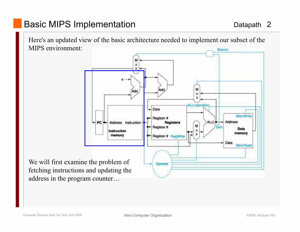
Datapath 2Basic MIPS Implementation
Here's an updated view of the basic architecture needed to implement our subset of the
MIPS environment:
Intro Computer OrganizationComputer Science Dept Va Tech April 2006 ©2006 McQuain WD
We will first examine the problem of
fetching instructions and updating the
address in the program counter…
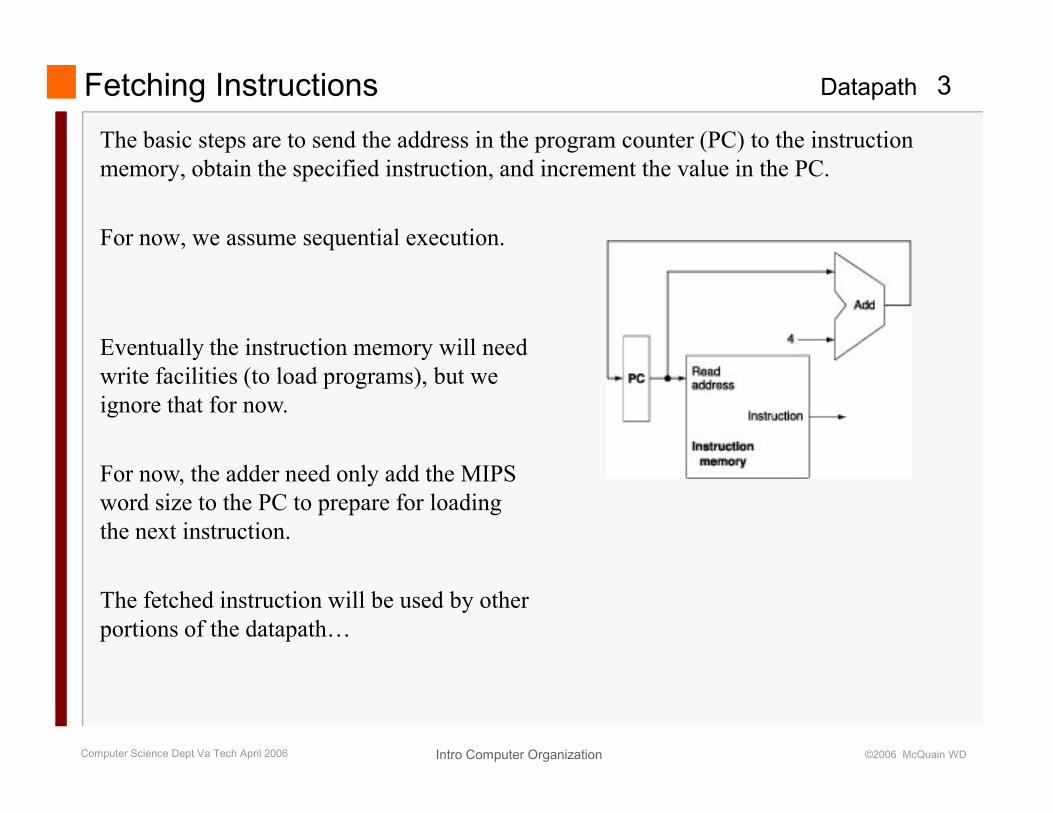
Datapath 3Fetching Instructions
The basic steps are to send the address in the program counter (PC) to the instruction
memory, obtain the specified instruction, and increment the value in the PC.
For now, we assume sequential execution.
Eventually the instruction memory will need
write facilities (to load programs), but we
ignore that for now.
Intro Computer OrganizationComputer Science Dept Va Tech April 2006 ©2006 McQuain WD
ignore that for now.
For now, the adder need only add the MIPS
word size to the PC to prepare for loading
the next instruction.
The fetched instruction will be used by other
portions of the datapath…
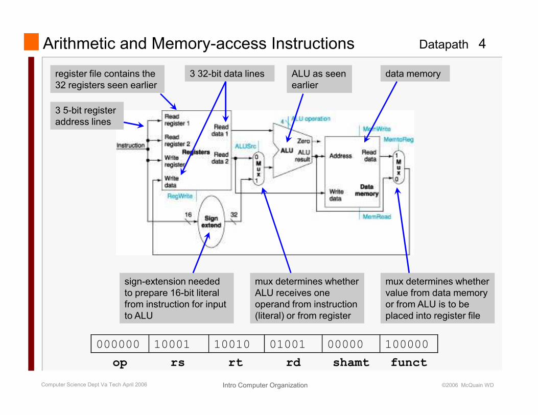
Datapath 4Arithmetic and Memory-access Instructions
3 5-bit register
address lines
register file contains the
32 registers seen earlier
3 32-bit data lines ALU as seen
earlier
data memory
Intro Computer OrganizationComputer Science Dept Va Tech April 2006 ©2006 McQuain WD
mux determines whether
ALU receives one
operand from instruction
(literal) or from register
mux determines whether
value from data memory
or from ALU is to be
placed into register file
sign-extension needed
to prepare 16-bit literal
from instruction for input
to ALU
10000000000010011001010001000000
functshamtrdrtrsop
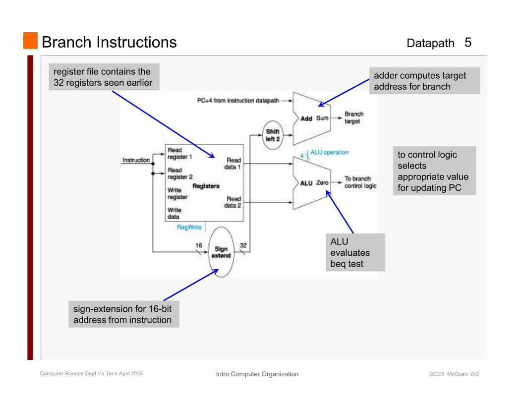
Datapath 5Branch Instructions
register file contains the
32 registers seen earlier
to control logic
selects
appropriate value
for updating PC
adder computes target
address for branch
Intro Computer OrganizationComputer Science Dept Va Tech April 2006 ©2006 McQuain WD
ALU
evaluates
beq test
sign-extension for 16-bit
address from instruction
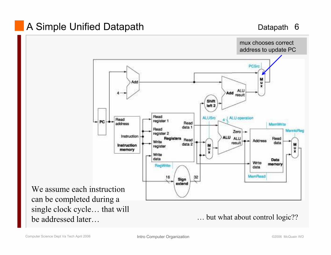
Datapath 6A Simple Unified Datapath
mux chooses correct
address to update PC
Intro Computer OrganizationComputer Science Dept Va Tech April 2006 ©2006 McQuain WD
We assume each instruction
can be completed during a
single clock cycle… that will
be addressed later… … but what about control logic??
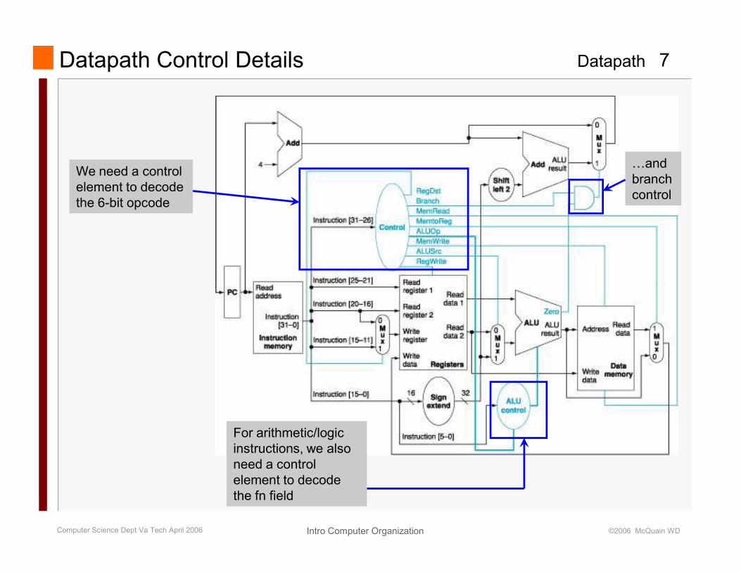
Datapath 7Datapath Control Details
We need a control
element to decode
the 6-bit opcode
…and
branch
control
Intro Computer OrganizationComputer Science Dept Va Tech April 2006 ©2006 McQuain WD
For arithmetic/logic
instructions, we also
need a control
element to decode
the fn field
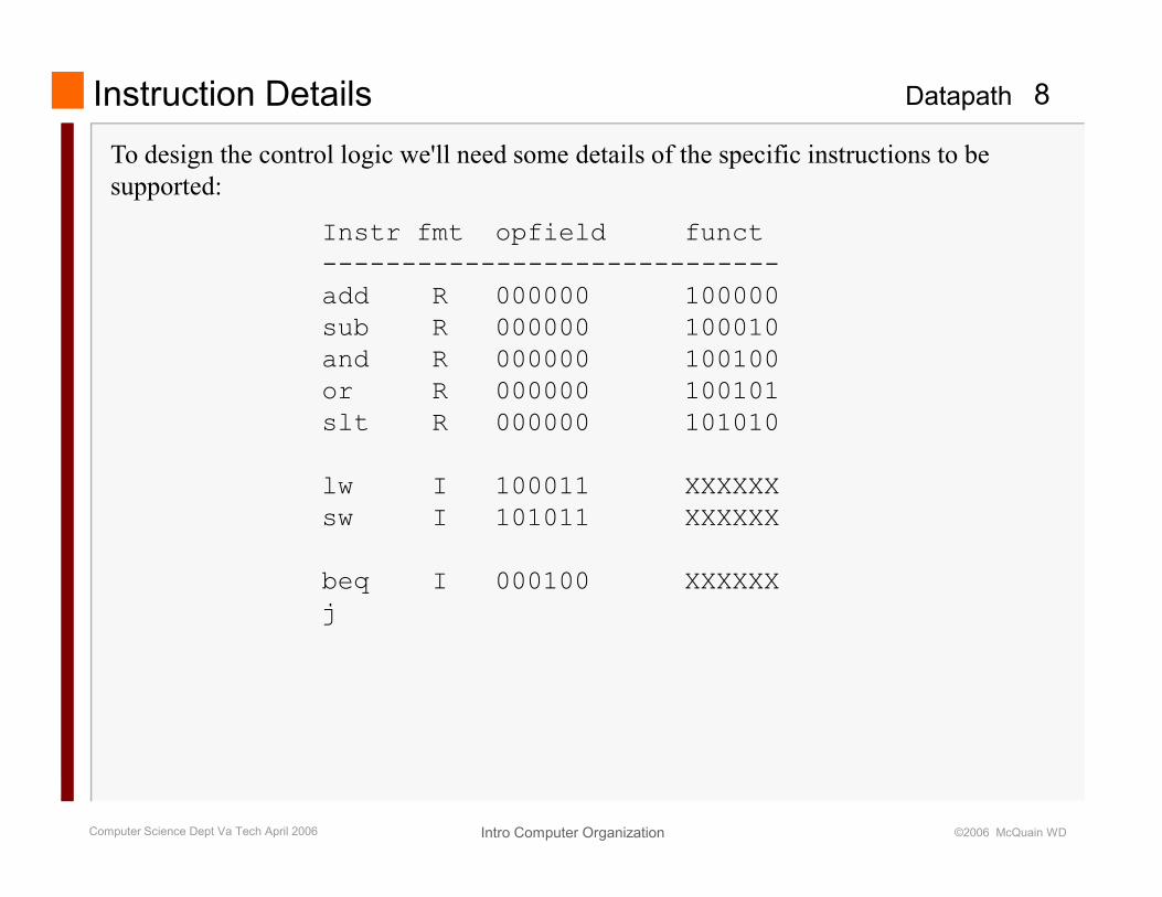
Datapath 8Instruction Details
To design the control logic we'll need some details of the specific instructions to be
supported:
Instr fmt opfield funct
-----------------------------
add R 000000 100000
sub R 000000 100010
and R 000000 100100
or R 000000 100101
slt R 000000 101010
Intro Computer OrganizationComputer Science Dept Va Tech April 2006 ©2006 McQuain WD
lw I 100011 XXXXXX
sw I 101011 XXXXXX
beq I 000100 XXXXXX
j
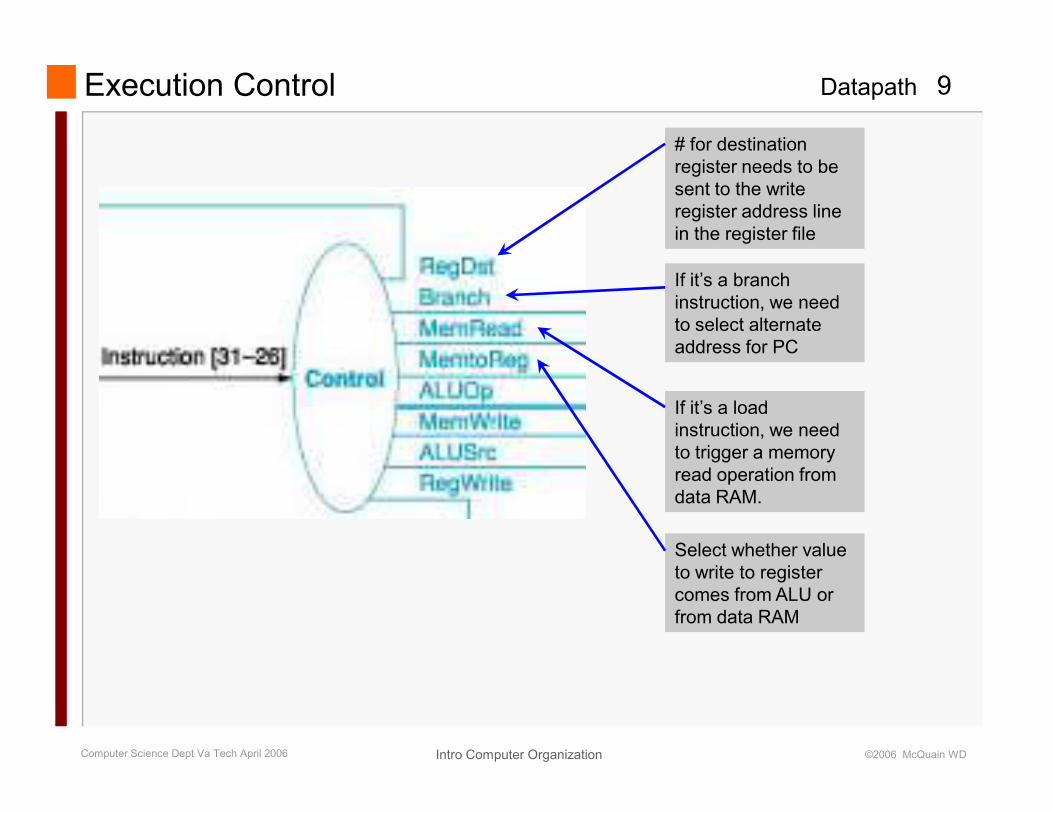
Datapath 9Execution Control
# for destination
register needs to be
sent to the write
register address line
in the register file
If it’s a branch
instruction, we need
to select alternate
address for PC
If it’s a load
Intro Computer OrganizationComputer Science Dept Va Tech April 2006 ©2006 McQuain WD
If it’s a load
instruction, we need
to trigger a memory
read operation from
data RAM.
Select whether value
to write to register
comes from ALU or
from data RAM
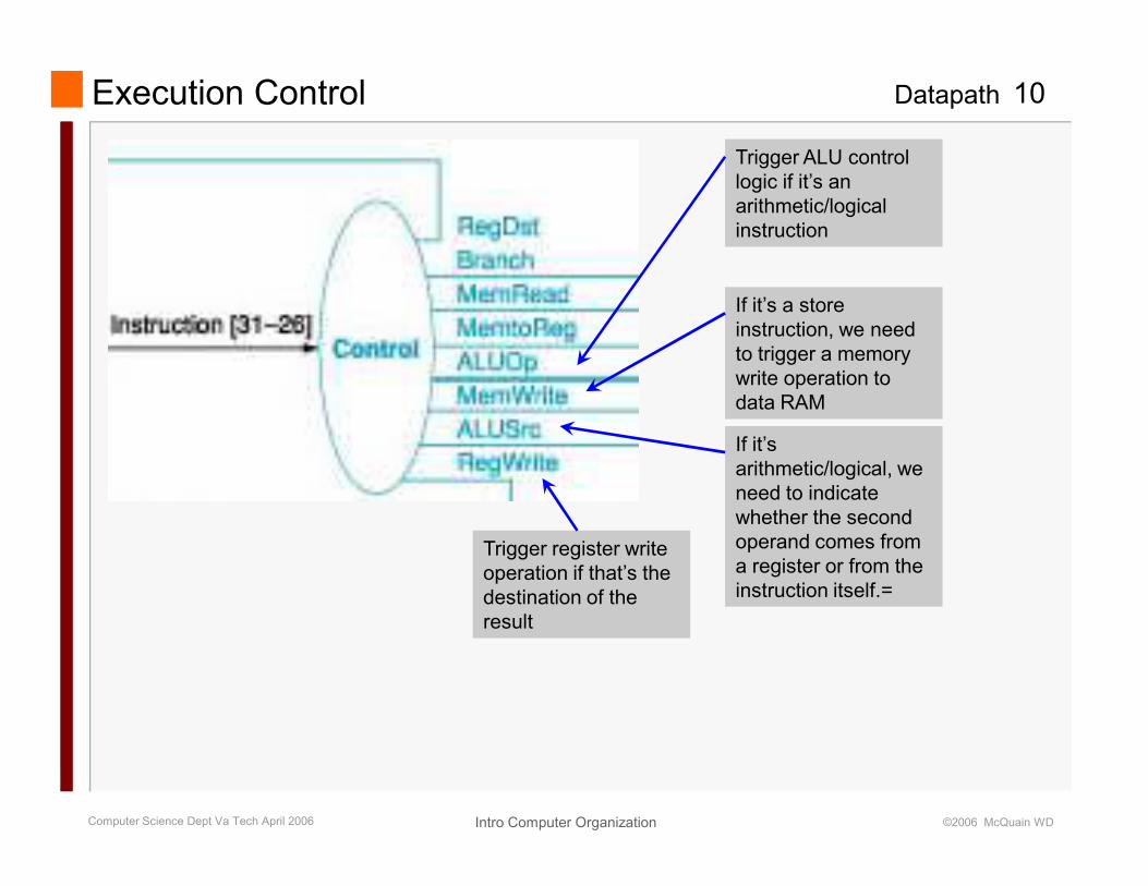
Datapath 10Execution Control
Trigger ALU control
logic if it’s an
arithmetic/logical
instruction
If it’s a store
instruction, we need
to trigger a memory
write operation to
data RAM
If it’s
Intro Computer OrganizationComputer Science Dept Va Tech April 2006 ©2006 McQuain WD
If it’s
arithmetic/logical, we
need to indicate
whether the second
operand comes from
a register or from the
instruction itself.=
Trigger register write
operation if that’s the
destination of the
result
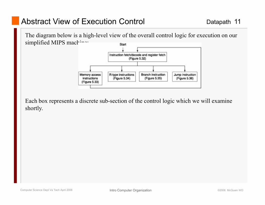
Datapath 11Abstract View of Execution Control
The diagram below is a high-level view of the overall control logic for execution on our
simplified MIPS machine:
Each box represents a discrete sub-section of the control logic which we will examine
Intro Computer OrganizationComputer Science Dept Va Tech April 2006 ©2006 McQuain WD
Each box represents a discrete sub-section of the control logic which we will examine
shortly.
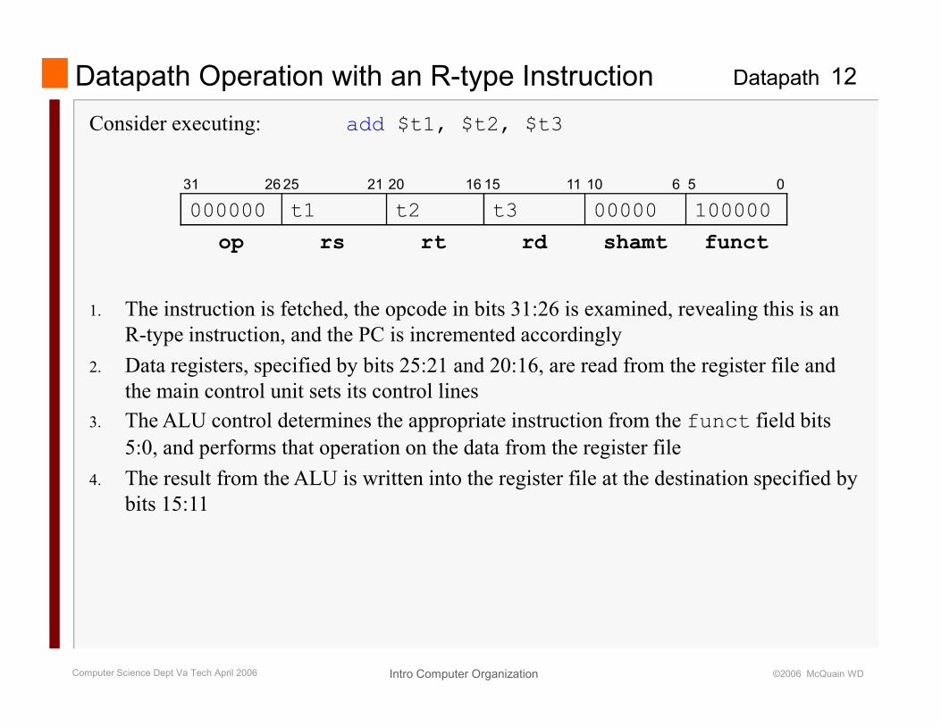
Datapath 12Datapath Operation with an R-type Instruction
Consider executing: add $t1, $t2, $t3
1. The instruction is fetched, the opcode in bits 31:26 is examined, revealing this is an
R-type instruction, and the PC is incremented accordingly
2. Data registers, specified by bits 25:21 and 20:16, are read from the register file and
10000000000t3t2t1000000
functshamtrdrtrsop
31 2625 21 20 16 15 11 10 6 5 0
Intro Computer OrganizationComputer Science Dept Va Tech April 2006 ©2006 McQuain WD
2. Data registers, specified by bits 25:21 and 20:16, are read from the register file and
the main control unit sets its control lines
3. The ALU control determines the appropriate instruction from the funct field bits
5:0, and performs that operation on the data from the register file
4. The result from the ALU is written into the register file at the destination specified by
bits 15:11
Datapath 13
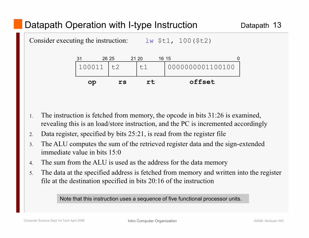
Consider executing the instruction: lw $t1, 100($t2)
Datapath Operation with I-type Instruction
1. The instruction is fetched from memory, the opcode in bits 31:26 is examined,
offsetrtrsop
0000000001100100t1t2100011
31 26 25 21 20 16 15 0
Intro Computer OrganizationComputer Science Dept Va Tech April 2006 ©2006 McQuain WD
The instruction is fetched from memory, the opcode in bits 31:26 is examined,
revealing this is an load/store instruction, and the PC is incremented accordingly
2. Data register, specified by bits 25:21, is read from the register file
3. The ALU computes the sum of the retrieved register data and the sign-extended
immediate value in bits 15:0
4. The sum from the ALU is used as the address for the data memory
5. The data at the specified address is fetched from memory and written into the register
file at the destination specified in bits 20:16 of the instruction
Note that this instruction uses a sequence of five functional processor units.
Datapath 14
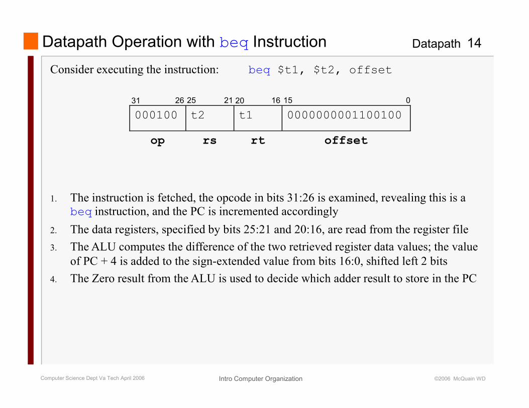
Consider executing the instruction: beq $t1, $t2, offset
Datapath Operation with beq Instruction
offsetrtrsop
0000000001100100t1t2000100
31 26 25 21 20 16 15 0
1. The instruction is fetched, the opcode in bits 31:26 is examined, revealing this is a
Intro Computer OrganizationComputer Science Dept Va Tech April 2006 ©2006 McQuain WD
The instruction is fetched, the opcode in bits 31:26 is examined, revealing this is a beq instruction, and the PC is incremented accordingly
2. The data registers, specified by bits 25:21 and 20:16, are read from the register file
3. The ALU computes the difference of the two retrieved register data values; the value
of PC + 4 is added to the sign-extended value from bits 16:0, shifted left 2 bits
4. The Zero result from the ALU is used to decide which adder result to store in the PC
Datapath 15
That is unrealistic.
- The clock cycle would be determined by the longest possible path in the machine
(which seems to be the path for a load instruction).
- Many instructions take much shorter paths through the machine, and so could be
executed in a shorter cycle… not doing so would reduce efficiency.
Single-cycle vs Multi-cycle Implementation
Up to this point, we have considered a design plan that will use a single clock cycle for
fetching and executing each instruction.
Intro Computer OrganizationComputer Science Dept Va Tech April 2006 ©2006 McQuain WD
A multi-cycle design allows instructions to take several clock cycles, and for the number
to vary from one instruction to another. In this case, this appears to be preferable.
Each step in the execution of an instruction will take one clock cycle.
But, what are the ramifications for the simplified design we have seen?
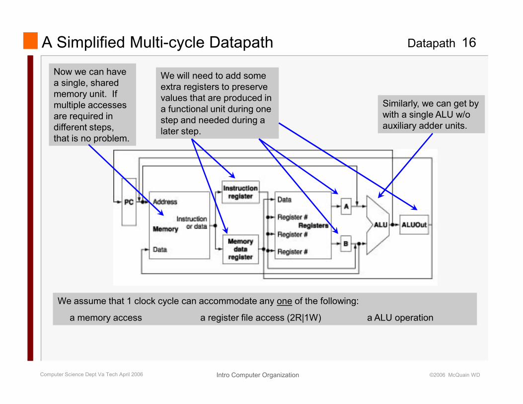
Datapath 16A Simplified Multi-cycle Datapath
Similarly, we can get by
with a single ALU w/o
auxiliary adder units.
We will need to add some
extra registers to preserve
values that are produced in
a functional unit during one
step and needed during a
later step.
Now we can have
a single, shared
memory unit. If
multiple accesses
are required in
different steps,
that is no problem.
Intro Computer OrganizationComputer Science Dept Va Tech April 2006 ©2006 McQuain WD
We assume that 1 clock cycle can accommodate any one of the following:
a memory access a register file access (2R|1W) a ALU operation
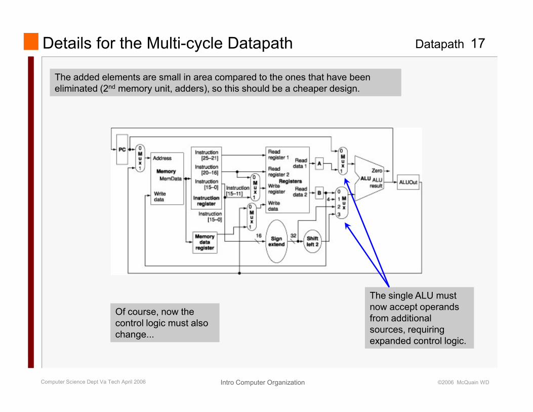
Datapath 17Details for the Multi-cycle Datapath
The added elements are small in area compared to the ones that have been
eliminated (2nd memory unit, adders), so this should be a cheaper design.
Intro Computer OrganizationComputer Science Dept Va Tech April 2006 ©2006 McQuain WD
The single ALU must
now accept operands
from additional
sources, requiring
expanded control logic.
Of course, now the
control logic must also
change...
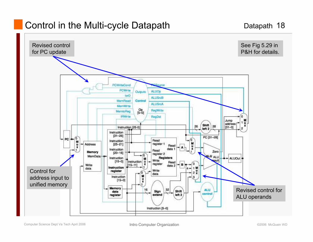
Datapath 18Control in the Multi-cycle Datapath
Revised control
for PC update
See Fig 5.29 in
P&H for details.
Intro Computer OrganizationComputer Science Dept Va Tech April 2006 ©2006 McQuain WD
Control for
address input to
unified memoryRevised control for
ALU operands
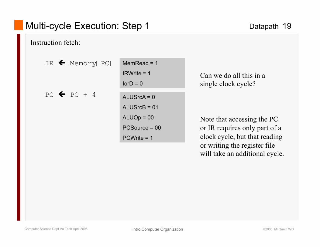
Datapath 19Multi-cycle Execution: Step 1
Instruction fetch:
IR � Memory[PC]
PC � PC + 4
MemRead = 1
IRWrite = 1
IorD = 0
ALUSrcA = 0
ALUSrcB = 01
ALUOp = 00
Can we do all this in a single clock cycle?
Note that accessing the PC
Intro Computer OrganizationComputer Science Dept Va Tech April 2006 ©2006 McQuain WD
PCSource = 00
PCWrite = 1
or IR requires only part of a
clock cycle, but that reading
or writing the register file will take an additional cycle.
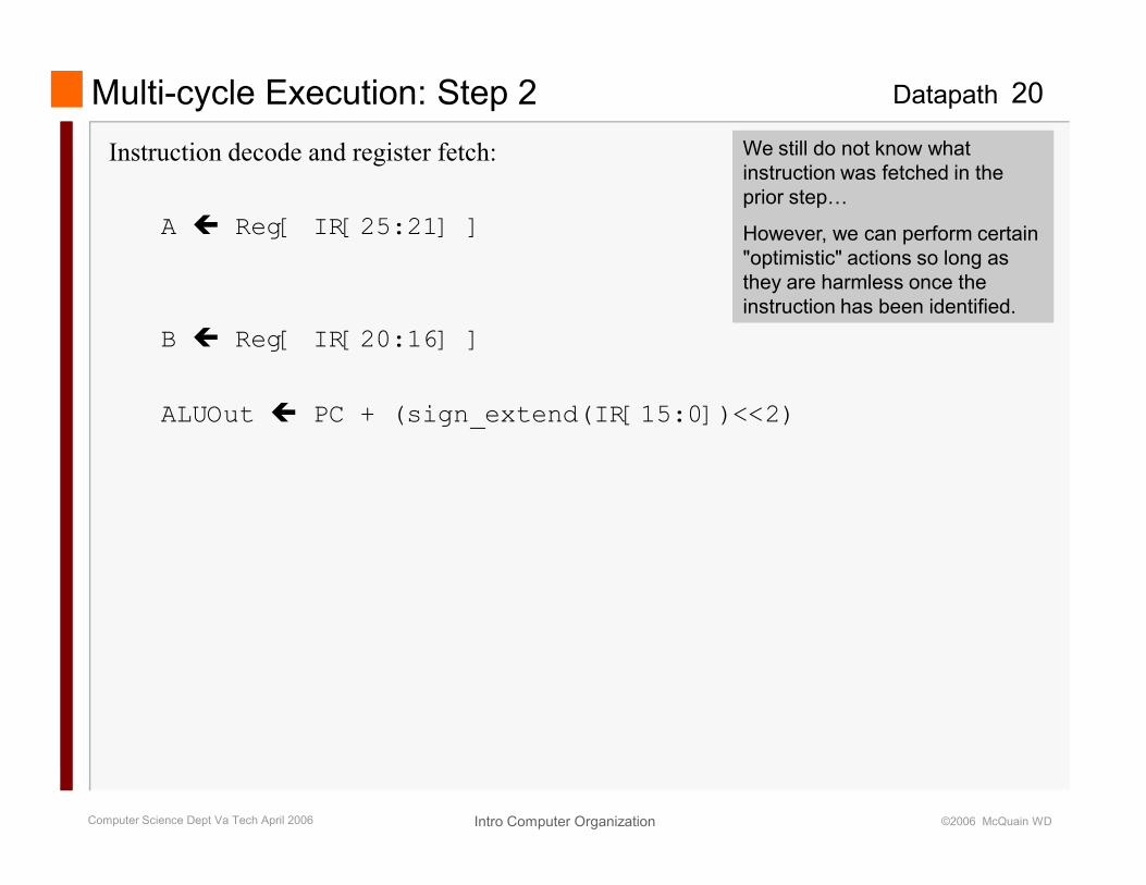
Datapath 20Multi-cycle Execution: Step 2
Instruction decode and register fetch:
A � Reg[ IR[25:21] ]
B � Reg[ IR[20:16] ]
ALUOut � PC + (sign_extend(IR[15:0])<<2)
We still do not know what
instruction was fetched in the
prior step…
However, we can perform certain
"optimistic" actions so long as
they are harmless once the
instruction has been identified.
Intro Computer OrganizationComputer Science Dept Va Tech April 2006 ©2006 McQuain WD
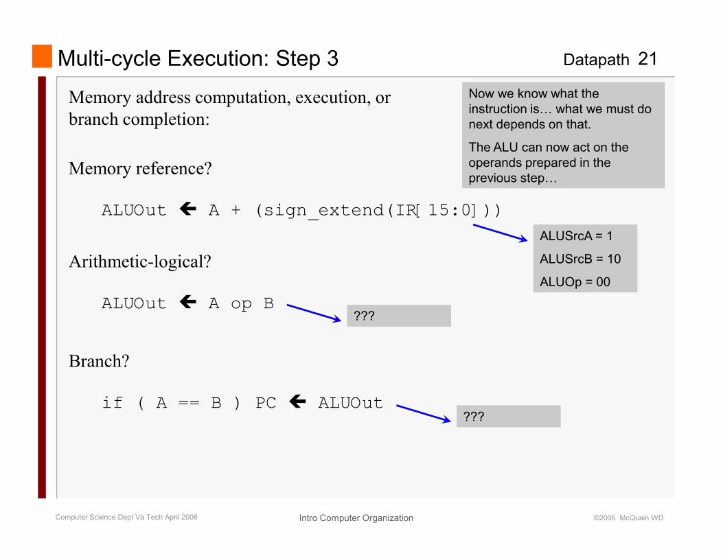
Datapath 21Multi-cycle Execution: Step 3
Memory address computation, execution, or
branch completion:
Now we know what the
instruction is… what we must do
next depends on that.
The ALU can now act on the
operands prepared in the
previous step…Memory reference?
ALUOut � A + (sign_extend(IR[15:0]))
Arithmetic-logical?
ALUSrcA = 1
ALUSrcB = 10
ALUOp = 00
Intro Computer OrganizationComputer Science Dept Va Tech April 2006 ©2006 McQuain WD
ALUOut � A op B
Branch?
if ( A == B ) PC � ALUOut
ALUOp = 00
???
???
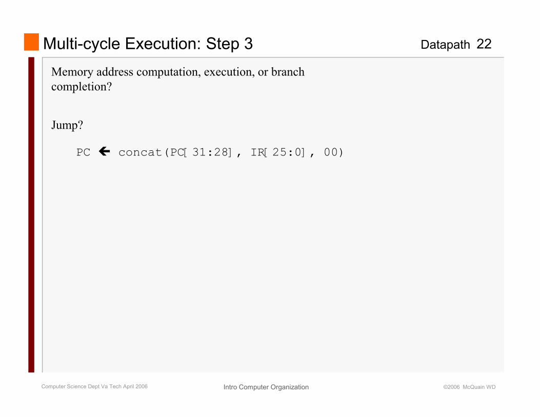
Datapath 22Multi-cycle Execution: Step 3
Memory address computation, execution, or branch
completion?
Jump?
PC � concat(PC[31:28], IR[25:0], 00)
Intro Computer OrganizationComputer Science Dept Va Tech April 2006 ©2006 McQuain WD
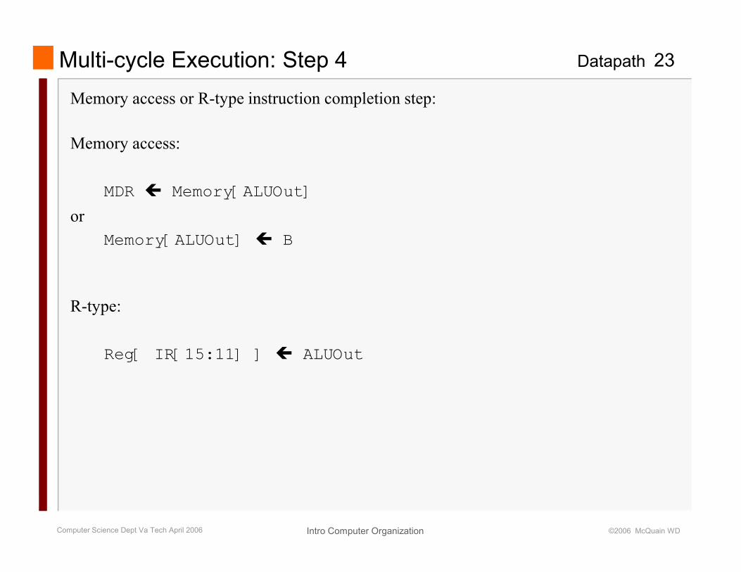
Datapath 23Multi-cycle Execution: Step 4
Memory access or R-type instruction completion step:
Memory access:
MDR � Memory[ALUOut]
or
Memory[ALUOut] � B
Intro Computer OrganizationComputer Science Dept Va Tech April 2006 ©2006 McQuain WD
R-type:
Reg[ IR[15:11] ] � ALUOut
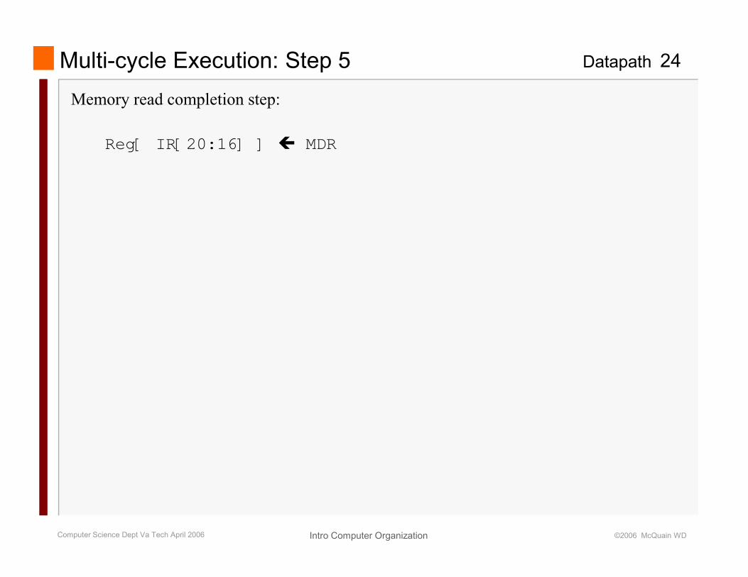
Datapath 24Multi-cycle Execution: Step 5
Memory read completion step:
Reg[ IR[20:16] ] � MDR
Intro Computer OrganizationComputer Science Dept Va Tech April 2006 ©2006 McQuain WD
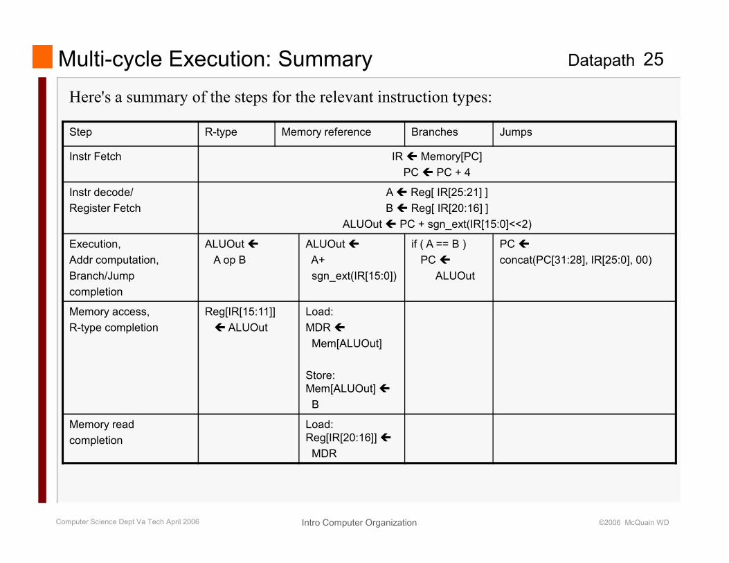
Datapath 25Multi-cycle Execution: Summary
Here's a summary of the steps for the relevant instruction types:
Step R-type Memory reference Branches Jumps
Instr Fetch IR � Memory[PC]
PC � PC + 4
Instr decode/
Register Fetch
A � Reg[ IR[25:21] ]
B � Reg[ IR[20:16] ]
ALUOut � PC + sgn_ext(IR[15:0]<<2)
Execution,
Addr computation,
Branch/Jump
ALUOut �
A op B
ALUOut �
A+
sgn_ext(IR[15:0])
if ( A == B )
PC �
ALUOut
PC �
concat(PC[31:28], IR[25:0], 00)
Intro Computer OrganizationComputer Science Dept Va Tech April 2006 ©2006 McQuain WD
Branch/Jump
completion
sgn_ext(IR[15:0]) ALUOut
Memory access,
R-type completion
Reg[IR[15:11]]
� ALUOut
Load:
MDR �
Mem[ALUOut]
Store:
Mem[ALUOut] �
B
Memory read
completion
Load:
Reg[IR[20:16]] �
MDR
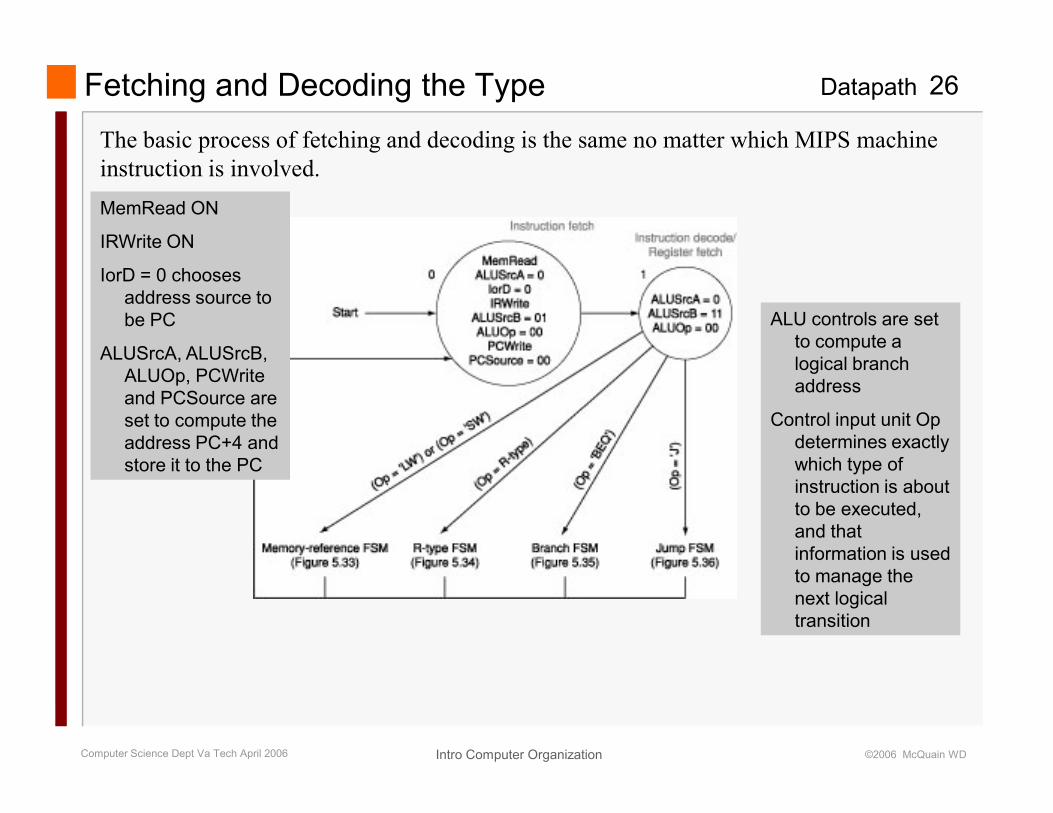
Datapath 26Fetching and Decoding the Type
The basic process of fetching and decoding is the same no matter which MIPS machine
instruction is involved.
MemRead ON
IRWrite ON
IorD = 0 chooses
address source to
be PC
ALUSrcA, ALUSrcB,
ALUOp, PCWrite
and PCSource are
ALU controls are set
to compute a
logical branch
address
Intro Computer OrganizationComputer Science Dept Va Tech April 2006 ©2006 McQuain WD
and PCSource are
set to compute the
address PC+4 and
store it to the PC
Control input unit Op
determines exactly
which type of
instruction is about
to be executed,
and that
information is used
to manage the
next logical
transition
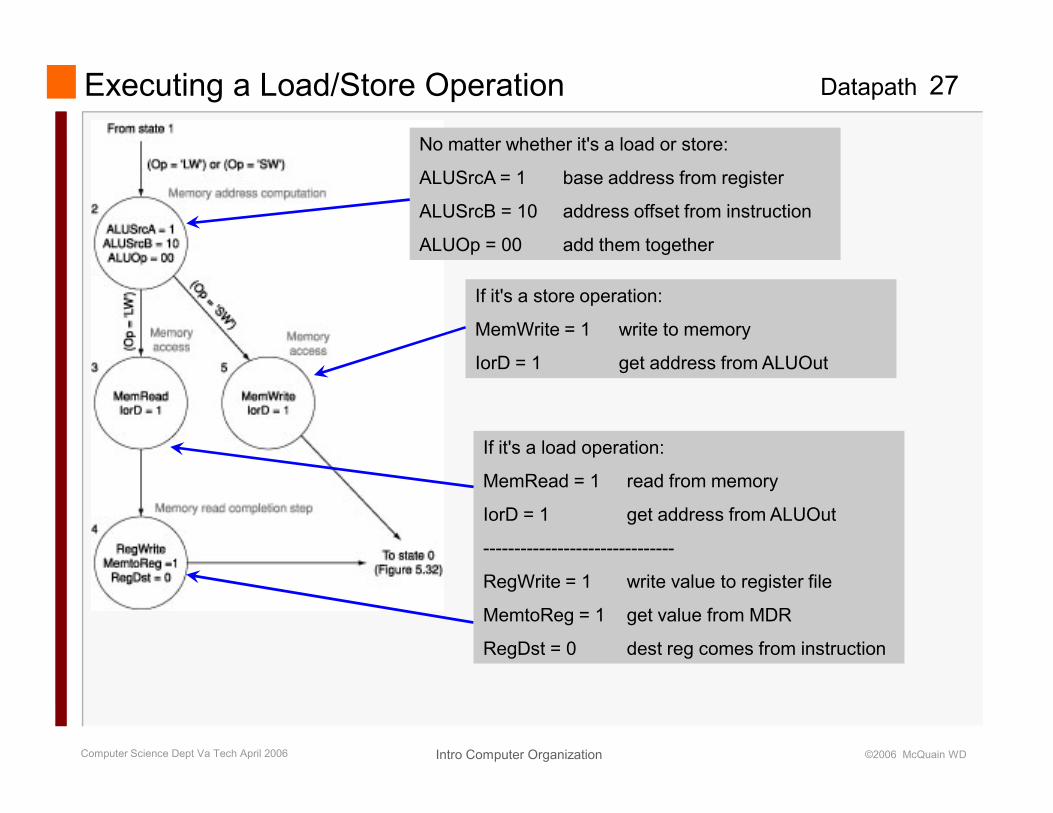
Datapath 27Executing a Load/Store Operation
No matter whether it's a load or store:
ALUSrcA = 1 base address from register
ALUSrcB = 10 address offset from instruction
ALUOp = 00 add them together
If it's a store operation:
MemWrite = 1 write to memory
IorD = 1 get address from ALUOut
Intro Computer OrganizationComputer Science Dept Va Tech April 2006 ©2006 McQuain WD
If it's a load operation:
MemRead = 1 read from memory
IorD = 1 get address from ALUOut
-------------------------------
RegWrite = 1 write value to register file
MemtoReg = 1 get value from MDR
RegDst = 0 dest reg comes from instruction
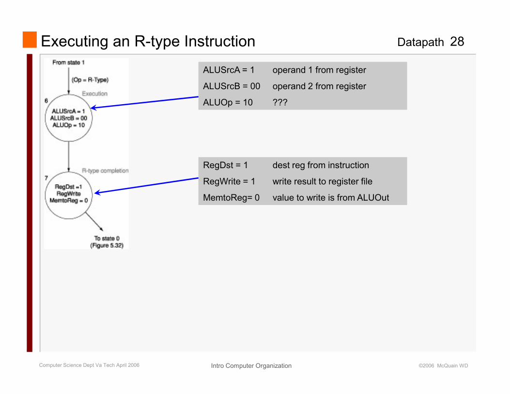
Datapath 28Executing an R-type Instruction
ALUSrcA = 1 operand 1 from register
ALUSrcB = 00 operand 2 from register
ALUOp = 10 ???
RegDst = 1 dest reg from instruction
RegWrite = 1 write result to register file
MemtoReg= 0 value to write is from ALUOut
Intro Computer OrganizationComputer Science Dept Va Tech April 2006 ©2006 McQuain WD
MemtoReg= 0 value to write is from ALUOut
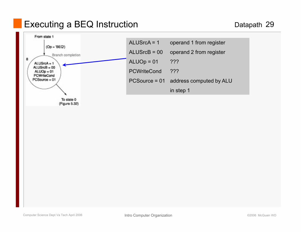
Datapath 29Executing a BEQ Instruction
ALUSrcA = 1 operand 1 from register
ALUSrcB = 00 operand 2 from register
ALUOp = 01 ???
PCWriteCond ???
PCSource = 01 address computed by ALU
in step 1
Intro Computer OrganizationComputer Science Dept Va Tech April 2006 ©2006 McQuain WD
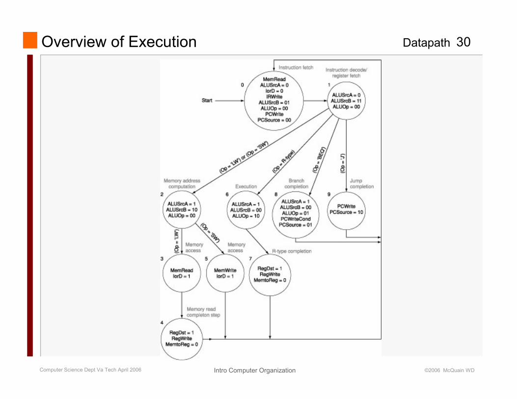
Datapath 30Overview of Execution
Intro Computer OrganizationComputer Science Dept Va Tech April 2006 ©2006 McQuain WD
Datapath 31Recall: Conceptual View of the ALU
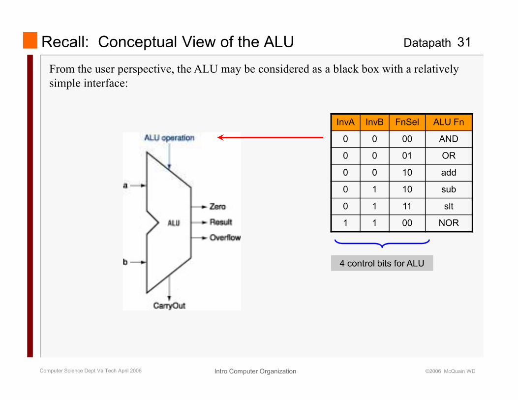
From the user perspective, the ALU may be considered as a black box with a relatively
simple interface:
InvA InvB FnSel ALU Fn
0 0 00 AND
0 0 01 OR
0 0 10 add
0 1 10 sub
Intro Computer OrganizationComputer Science Dept Va Tech April 2006 ©2006 McQuain WD
0 1 11 slt
1 1 00 NOR
4 control bits for ALU
Datapath 32ALU Control Function
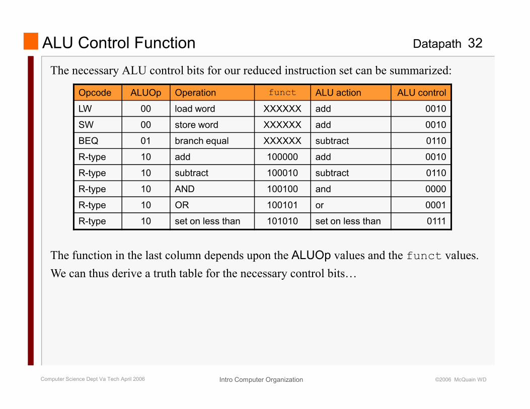
The necessary ALU control bits for our reduced instruction set can be summarized:
Opcode ALUOp Operation funct ALU action ALU control
LW 00 load word XXXXXX add 0010
SW 00 store word XXXXXX add 0010
BEQ 01 branch equal XXXXXX subtract 0110
R-type 10 add 100000 add 0010
R-type 10 subtract 100010 subtract 0110
R-type 10 AND 100100 and 0000
R-type 10 OR 100101 or 0001
Intro Computer OrganizationComputer Science Dept Va Tech April 2006 ©2006 McQuain WD
R-type 10 OR 100101 or 0001
R-type 10 set on less than 101010 set on less than 0111
The function in the last column depends upon the ALUOp values and the funct values.
We can thus derive a truth table for the necessary control bits…
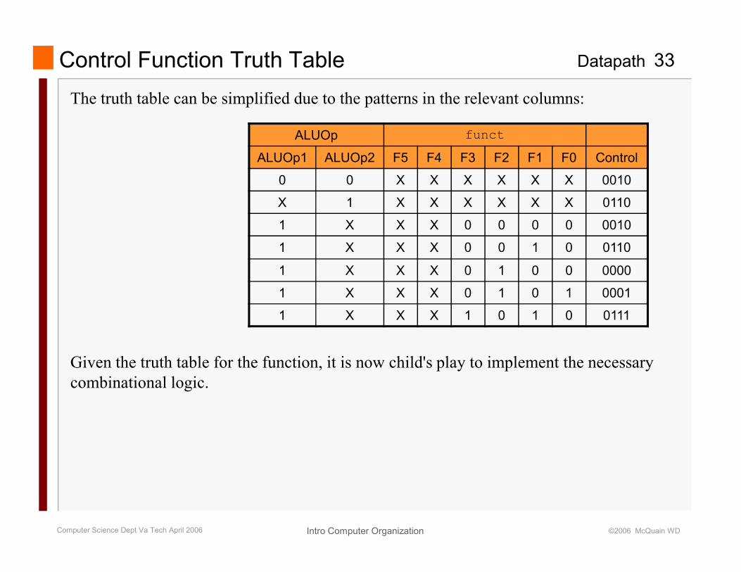
Datapath 33Control Function Truth Table
The truth table can be simplified due to the patterns in the relevant columns:
ALUOp funct
ALUOp1 ALUOp2 F5 F4 F3 F2 F1 F0 Control
0 0 X X X X X X 0010
X 1 X X X X X X 0110
1 X X X 0 0 0 0 0010
1 X X X 0 0 1 0 0110
1 X X X 0 1 0 0 0000
1 X X X 0 1 0 1 0001
Intro Computer OrganizationComputer Science Dept Va Tech April 2006 ©2006 McQuain WD
Given the truth table for the function, it is now child's play to implement the necessary
combinational logic.
1 X X X 0 1 0 1 0001
1 X X X 1 0 1 0 0111
Datapath 34ALU Control Block
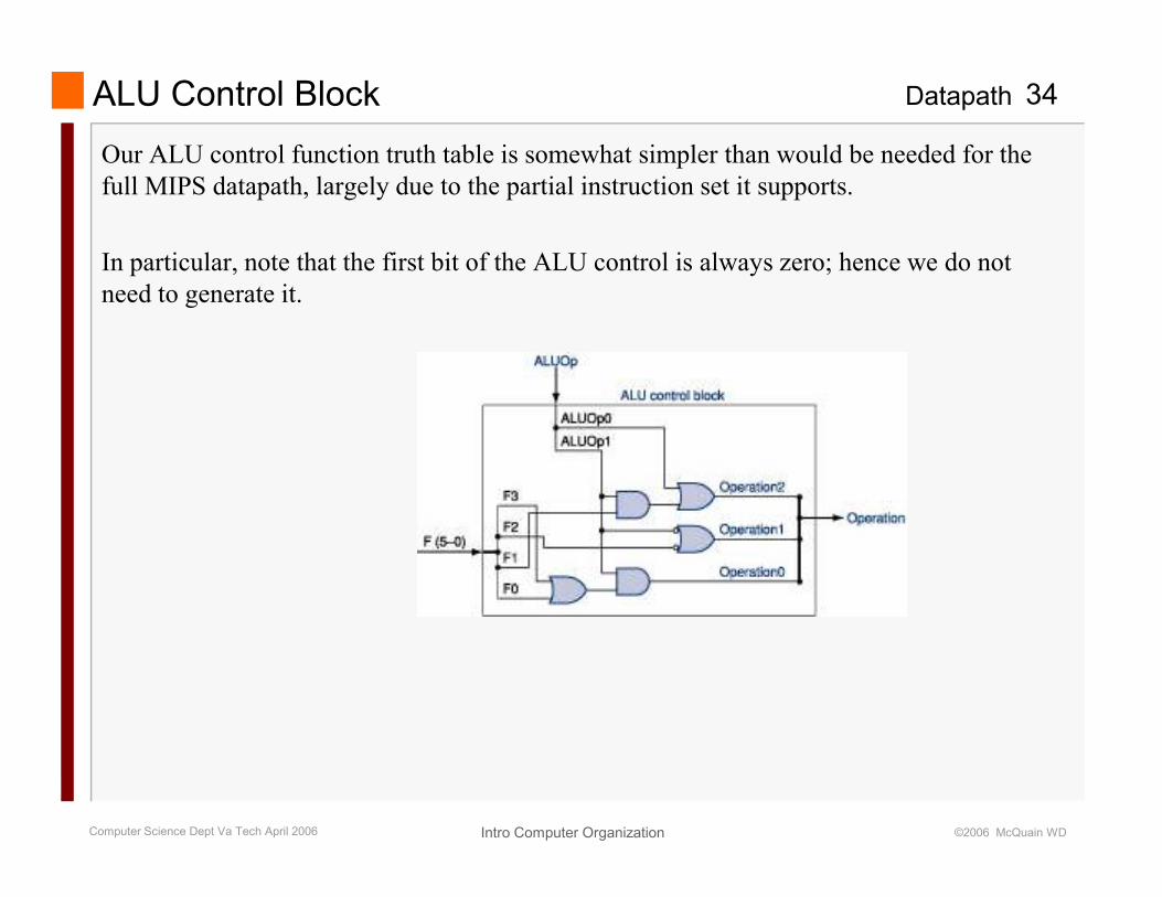
Our ALU control function truth table is somewhat simpler than would be needed for the
full MIPS datapath, largely due to the partial instruction set it supports.
In particular, note that the first bit of the ALU control is always zero; hence we do not
need to generate it.
Intro Computer OrganizationComputer Science Dept Va Tech April 2006 ©2006 McQuain WD
Datapath 35
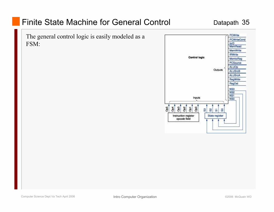
The general control logic is easily modeled as a
FSM:
Finite State Machine for General Control
Intro Computer OrganizationComputer Science Dept Va Tech April 2006 ©2006 McQuain WD
Datapath 36General Control Logic as a PLA
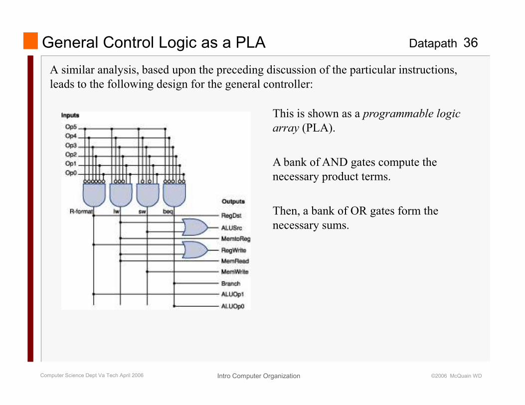
A similar analysis, based upon the preceding discussion of the particular instructions,
leads to the following design for the general controller:
This is shown as a programmable logic
array (PLA).
A bank of AND gates compute the
necessary product terms.
Intro Computer OrganizationComputer Science Dept Va Tech April 2006 ©2006 McQuain WD
Then, a bank of OR gates form the
necessary sums.
Datapath 37
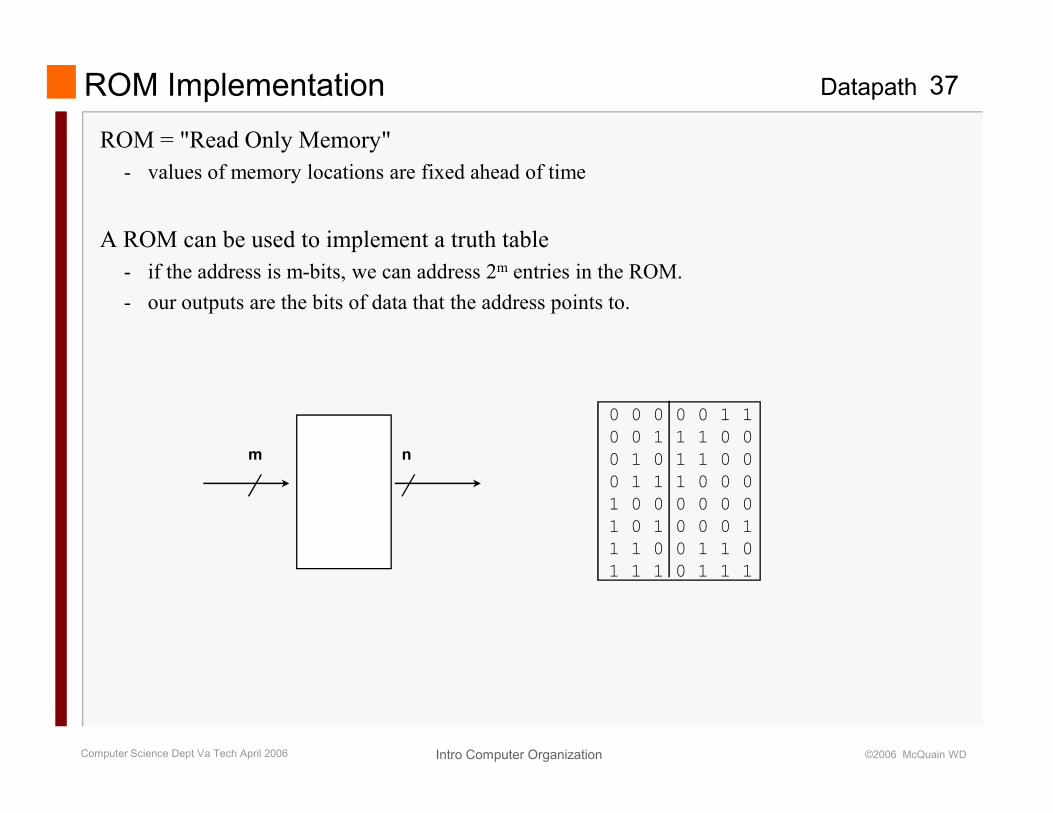
ROM = "Read Only Memory"
- values of memory locations are fixed ahead of time
A ROM can be used to implement a truth table
- if the address is m-bits, we can address 2m entries in the ROM.
- our outputs are the bits of data that the address points to.
ROM Implementation
0 0 0 0 0 1 1
Intro Computer OrganizationComputer Science Dept Va Tech April 2006 ©2006 McQuain WD
m n
0 0 0 0 0 1 1
0 0 1 1 1 0 0
0 1 0 1 1 0 0
0 1 1 1 0 0 0
1 0 0 0 0 0 0
1 0 1 0 0 0 1
1 1 0 0 1 1 0
1 1 1 0 1 1 1
Datapath 38
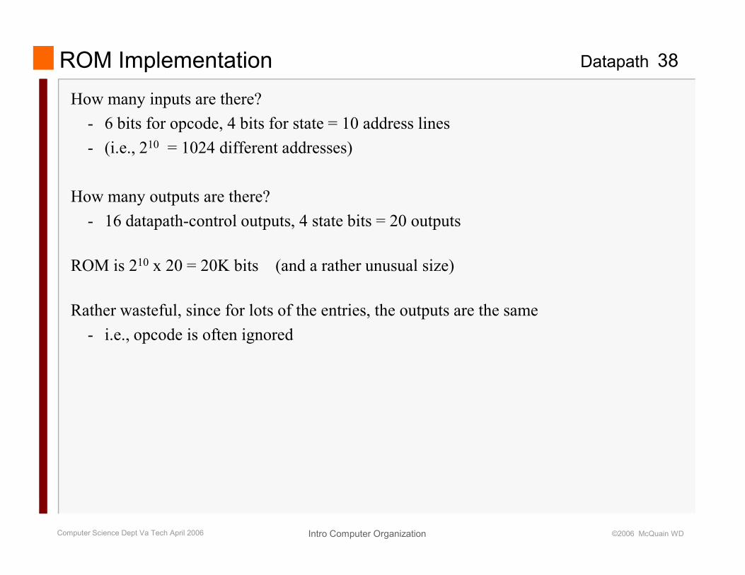
How many inputs are there?
- 6 bits for opcode, 4 bits for state = 10 address lines
- (i.e., 210 = 1024 different addresses)
How many outputs are there?
- 16 datapath-control outputs, 4 state bits = 20 outputs
ROM is 210 x 20 = 20K bits (and a rather unusual size)
ROM Implementation
Intro Computer OrganizationComputer Science Dept Va Tech April 2006 ©2006 McQuain WD
Rather wasteful, since for lots of the entries, the outputs are the same
- i.e., opcode is often ignored
Datapath 39
Break up the table into two parts
- 4 state bits tell you the 16 outputs, 24 x 16 bits of ROM
- 10 bits tell you the 4 next state bits, 210 x 4 bits of ROM
- total: 4.3K bits of ROM
PLA is much smaller
- can share product terms
ROM vs PLA
Intro Computer OrganizationComputer Science Dept Va Tech April 2006 ©2006 McQuain WD
- only need entries that produce an active output
- can take into account don't cares
Size is (#inputs × #product-terms) + (#outputs × #product-terms)
- for this example = (10x17)+(20x17) = 510 PLA cells
PLA cells usually about the size of a ROM cell (slightly bigger)