Embed Size (px)
Citation preview
Journal of Crystal Growth 189/190 (1998) 344—348
MOVPE growth of high quality III-nitride material for lightemitting device applications in a multiwafer system
Caspar von Eichel-Streiber!, Oliver Schon!,",*, Rainer Beccard!, Dietmar Schmitz!,Michael Heuken!,", Holger Jurgensen!
! AIXTRON AG, Kackertstr. 15–17, D-52072 Aachen, Germany" Institut fu( r Halbleitertechnik, RWTH Aachen, Templergraben 55, D-52056 Aachen, Germany
Abstract
Processes for mass production of GaN and its related alloys, InGaN and AlGaN, have been optimized to achieve highdevice yield and low cost of ownership. Here we present some of the latest results obtained from AIX 2000HT PlanetaryReactorst in a configuration of 7]2A which provides unique uniformity capabilities due to the twofold rotation of thesubstrates. GaN single layers with background electron concentrations below 5]1016 cm~3 and intended doping levelsup to 1018 cm~3 p-type and 1020 cm~3 n-type with state of the art homogeneities have been achieved. Thicknesshomogeneities have been shown to be better than 1% standard deviation on full 2A wafers, while composition uniformityof ternary material is determined by room temperature photoluminescence mappings. Low-temperature photolumines-cence and reflectance spectra of single-layer GaN revealed free-exciton transitions ( 1998 Elsevier Science B.V. Allrights reserved.
1. Introduction
Since GaN-based materials developed from re-search challenges to topics for industrial produc-tion for short-wavelength optoelectronics [1] thePlanetary Reactort design has been adapted tomeet the demands for multiwafer systems with highyield and throughput at the high growth temper-atures required for the deposition of this materialsystem. Key aspects of the processes for device
*Corresponding author. Fax: #49 241 89 09 40; e-mail:[email protected].
fabrication are high quality and excellent homo-geneity of the individual layers. To this end, growthconditions have been optimized regarding total andprecursor flows, total pressure and growth temper-ature.
2. Sample preparation
The results presented here were obtained fromsingle-layer GaN on sapphire samples and simpleAlGaN or GaInN on GaN (on sapphire) hetero-structures. The layers were grown on c-planesapphire in an AIX 2000HT Planetary Reactort,
0022-0248/98/$19.00 ( 1998 Elsevier Science B.V. All rights reserved.PII S 0 0 2 2 - 0 2 4 8 ( 9 8 ) 0 0 2 9 0 - 5
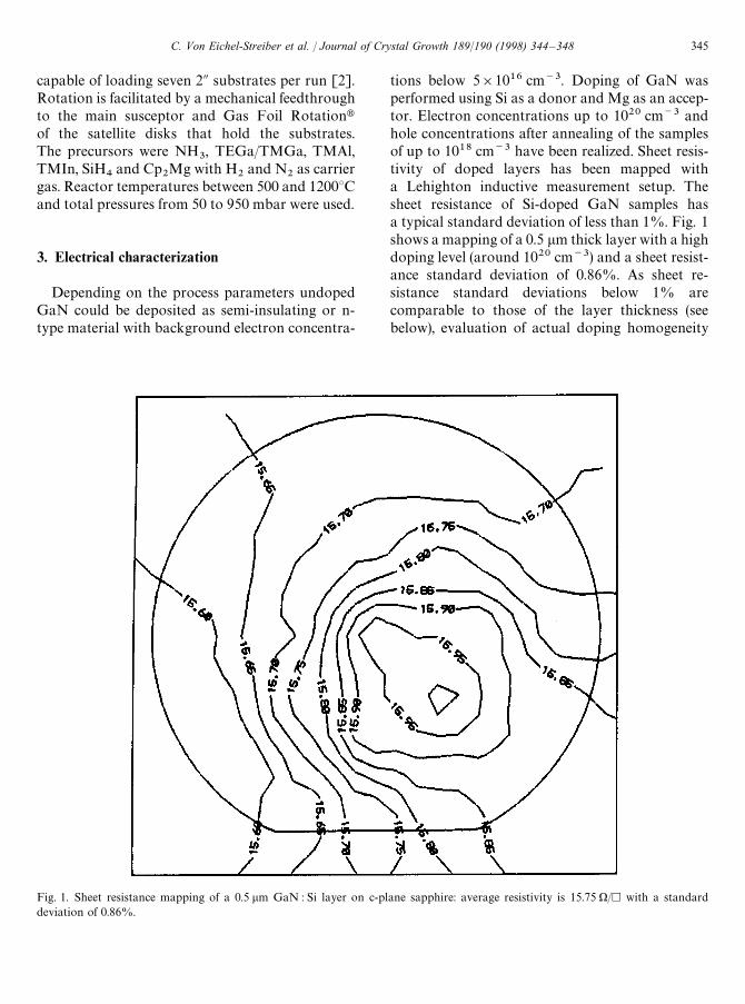
Fig. 1. Sheet resistance mapping of a 0.5 lm GaN : Si layer on c-plane sapphire: average resistivity is 15.75 )/h with a standarddeviation of 0.86%.
capable of loading seven 2A substrates per run [2].Rotation is facilitated by a mechanical feedthroughto the main susceptor and Gas Foil Rotationtof the satellite disks that hold the substrates.The precursors were NH
3, TEGa/TMGa, TMAl,
TMIn, SiH4
and Cp2Mg with H
2and N
2as carrier
gas. Reactor temperatures between 500 and 1200°Cand total pressures from 50 to 950 mbar were used.
3. Electrical characterization
Depending on the process parameters undopedGaN could be deposited as semi-insulating or n-type material with background electron concentra-
tions below 5]1016 cm~3. Doping of GaN wasperformed using Si as a donor and Mg as an accep-tor. Electron concentrations up to 1020 cm~3 andhole concentrations after annealing of the samplesof up to 1018 cm~3 have been realized. Sheet resis-tivity of doped layers has been mapped witha Lehighton inductive measurement setup. Thesheet resistance of Si-doped GaN samples hasa typical standard deviation of less than 1%. Fig. 1shows a mapping of a 0.5 lm thick layer with a highdoping level (around 1020 cm~3) and a sheet resist-ance standard deviation of 0.86%. As sheet re-sistance standard deviations below 1% arecomparable to those of the layer thickness (seebelow), evaluation of actual doping homogeneity
C. Von Eichel-Streiber et al. / Journal of Crystal Growth 189/190 (1998) 344–348 345
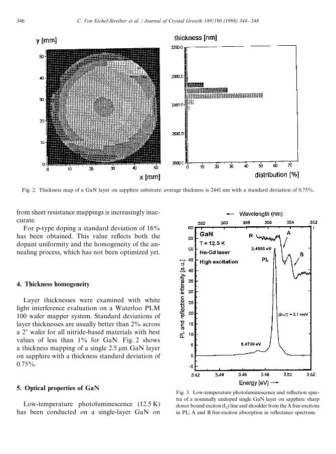
Fig. 2. Thickness map of a GaN layer on sapphire substrate: average thickness is 2441 nm with a standard deviation of 0.75%.
from sheet resistance mappings is increasingly inac-curate.
For p-type doping a standard deviation of 16%has been obtained. This value reflects both thedopant uniformity and the homogeneity of the an-nealing process, which has not been optimized yet.
4. Thickness homogeneity
Layer thicknesses were examined with whitelight interference evaluation on a Waterloo PLM100 wafer mapper system. Standard deviations oflayer thicknesses are usually better than 2% acrossa 2A wafer for all nitride-based materials with bestvalues of less than 1% for GaN. Fig. 2 showsa thickness mapping of a single 2.5 lm GaN layeron sapphire with a thickness standard deviation of0.75%.
5. Optical properties of GaN
Low-temperature photoluminescence (12.5 K)has been conducted on a single-layer GaN on
Fig. 3. Low-temperature photoluminescence and reflection spec-tra of a nominally undoped single GaN layer on sapphire: sharpdonor bound exciton (I
2) line and shoulder from the A free-excitons
in PL; A and B free-exciton absorption in reflectance spectrum.
346 C. Von Eichel-Streiber et al. / Journal of Crystal Growth 189/190 (1998) 344–348
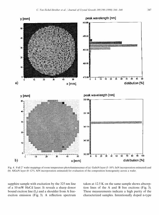
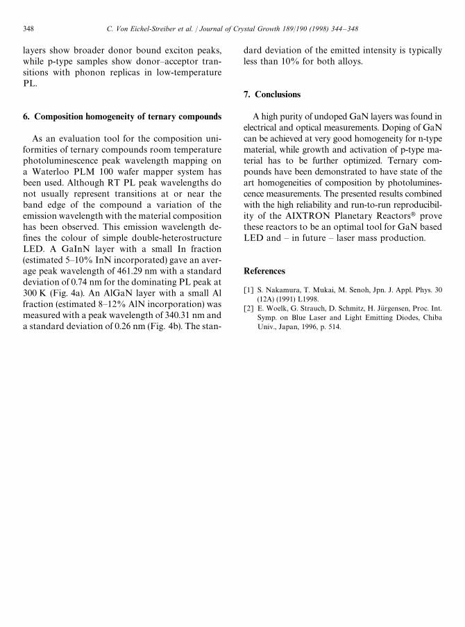
Fig. 4. Full 2A wafer mappings of room temperature photoluminescence of (a) GaInN layer (5—10% InN incorporation estimated) and(b) AlGaN layer (8—12% AlN incorporation estimated) for evaluation of the composition homogeneity across a wafer.
sapphire sample with excitation by the 325 nm lineof a 10 mW HeCd laser. It reveals a sharp donorbound exciton line (I
2) and a shoulder from A free-
exciton emission (Fig. 3). A reflection spectrum
taken at 12.5 K on the same sample shows absorp-tion lines of the A and B free excitons (Fig. 3).These measurements indicate a high purity of thecharacterized samples. Intentionally doped n-type
C. Von Eichel-Streiber et al. / Journal of Crystal Growth 189/190 (1998) 344–348 347
layers show broader donor bound exciton peaks,while p-type samples show donor—acceptor tran-sitions with phonon replicas in low-temperaturePL.
6. Composition homogeneity of ternary compounds
As an evaluation tool for the composition uni-formities of ternary compounds room temperaturephotoluminescence peak wavelength mapping ona Waterloo PLM 100 wafer mapper system hasbeen used. Although RT PL peak wavelengths donot usually represent transitions at or near theband edge of the compound a variation of theemission wavelength with the material compositionhas been observed. This emission wavelength de-fines the colour of simple double-heterostructureLED. A GaInN layer with a small In fraction(estimated 5—10% InN incorporated) gave an aver-age peak wavelength of 461.29 nm with a standarddeviation of 0.74 nm for the dominating PL peak at300 K (Fig. 4a). An AlGaN layer with a small Alfraction (estimated 8—12% AlN incorporation) wasmeasured with a peak wavelength of 340.31 nm anda standard deviation of 0.26 nm (Fig. 4b). The stan-
dard deviation of the emitted intensity is typicallyless than 10% for both alloys.
7. Conclusions
A high purity of undoped GaN layers was found inelectrical and optical measurements. Doping of GaNcan be achieved at very good homogeneity for n-typematerial, while growth and activation of p-type ma-terial has to be further optimized. Ternary com-pounds have been demonstrated to have state of theart homogeneities of composition by photolumines-cence measurements. The presented results combinedwith the high reliability and run-to-run reproducibil-ity of the AIXTRON Planetary Reactorst provethese reactors to be an optimal tool for GaN basedLED and — in future — laser mass production.
References
[1] S. Nakamura, T. Mukai, M. Senoh, Jpn. J. Appl. Phys. 30(12A) (1991) L1998.
[2] E. Woelk, G. Strauch, D. Schmitz, H. Jurgensen, Proc. Int.Symp. on Blue Laser and Light Emitting Diodes, ChibaUniv., Japan, 1996, p. 514.
348 C. Von Eichel-Streiber et al. / Journal of Crystal Growth 189/190 (1998) 344–348


![GaN-based light-emitting diodes with graphene/indium tin ... · green spectral regions [1,2]. For example, gallium nitride (GaN)-based blue and green light-emitting diodes (LEDs)](https://img.pdfslide.us/doc/110x75/5f02215f7e708231d402b8ad/gan-based-light-emitting-diodes-with-grapheneindium-tin-green-spectral-regions.jpg)