Embed Size (px)
Citation preview

Moshe Lopian Michael Sberro Ron Zarsky


Content-addressable memories (CAMs) are hardware search engines that are much faster than algorithmic approaches for search-intensive applications.
CAMs are composed of conventional semiconductor memory (usually SRAM) with added comparison circuitry that enable a search operation to complete in a single clock cycle.

applications where CAMs are used
Address lookup function in Internet routers. IP routing (internet protocol) Cache memory in microprocessors Pattern recognition in AI robotic systems Translation lookaside buffers (TLB) Real-time compression and Encryption Data compression applications Mapping Tables and translating buffers In microprocessors Database accelerators Neural networks .
We will give an extensive explanation of the advantage of CAM with the example of address lookup function in Internet routers.
Then we will give a short description of the use of the CAM in some of the other applications

Internet routers forward data packets from an incoming port using an address lookup function.
The address lookup function examines the packet's destination address and chooses an output port associated with that address. The router's list of destination addresses and their corresponding output ports is called the routing table.

Table 1: Simplified routing Table 1: Simplified routing table. table.
Line No. Line No. Address Address (Binary) (Binary)
Output Output Port Port
11 101XX 101XX AA
22 0110X 0110X BB
33 011XX 011XX CC
44 10011 10011 DD
An example of a simplified routing table
Table 1.

The routing parameters that determine the complexity of the implementation are:
Entry size Table size Search rate Table update rate.
Routing table sizes are about 30,000 entries but are growing rapidly. Routers must perform hundreds of millions of searches per second in addition to thousands of routing table updates per second.

All four entries in the table are 5-bit words, with the don't care bit, X. Because of the X bits, the first three entries in Table 1 represent a range of input addresses, i.e. the entry on Line 1 indicates that all addresses in the range of 10100—10111 are forwarded to port A. The router searches for the destination address of each incoming packet in the address lookup table to find the appropriate output port. For example, if the router receives a packet with the incoming address 01101, the address lookup matches both line 2 and Line 3 in the table. Line 2 is selected since it has the most defined bits, indicating it is the most direct route to the destination. This lookup style is called longest-prefix matching and is required to implement the most recent Internet Protocol (IP) networking standard.

There are many software-based methods to implement the address lookup function, although not all can meet the above requirements. For example, software-based binary searching accomplishes the task if the lookup table is ordered.
Binary searching has O(log n) time complexity in addition to the extra time required to insert a new entry in the table.
Almost all algorithmic approaches are too slow to keep up with projected routing requirements. In contrast, CAMs use hardware to complete a search in a single cycle, resulting in constant O(1) time complexity.
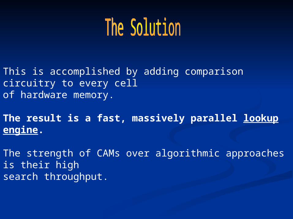
This is accomplished by adding comparison circuitry to every cell of hardware memory.
The result is a fast, massively parallel lookup engine.
The strength of CAMs over algorithmic approaches is their high search throughput.

The current bottleneck is the large power consumption due to the large amount of comparison circuitry activated in parallel.
Reducing the power consumption is a key aim of current CAM research.

There are two basic forms of CAM: binary ternary
Binary CAMs support storage and searching of binary bits, zero or one (0,1).
Ternary CAMs support storing of zero, one, or don't care bit (0,1,X).
Ternary CAMs are presently the dominant CAM since longest-prefix routing is the Internet standard.

Figure 1 shows a block diagram of a simplified 4 x 5 bit ternary CAM.
Figure 1

The CAM contains the routing table from Table 1 to illustrate how a CAM implements address lookup.
The CAM core cells are arranged into four horizontal words, each five bits long.
Core cells contain both storage and comparison circuitry. The search lines run vertically in the figure and broadcast the search data to the CAM cells.
b
b
~b
~bwlwl
~ddm
pre_charge
b1
b1
~b1
~b1wlwl
~d1dm1
b2
b2
~b2
~b2wlwl
~d2dm2
ml
Cam 3-bit word
Cam core cell

The matchlines run horizontally across the array and indicate whether the
search data matches the row's word. An activated matchline indicates a match and a deactivated matchline indicates a non-match, called a mismatch in the CAM literature. The matchlines are inputs to an encoder that generates the address corresponding to the match location.

Stage 1:A CAM search operation begins with precharging all matchlines high, putting them all temporarily in the match state.
Stage 2:the search line drivers broadcast the search data, 01101 in the figure, onto the search lines.
Stage 3:Then each CAM core cell compares its stored bit against the bit on its corresponding search lines.
Cells with matching data do not affect the matchline but cells with a mismatch pull down the matchline.
Cells storing an X operate as if a match has occurred.
The result is that matchlines are pulled down for any word that has at least one mismatch.
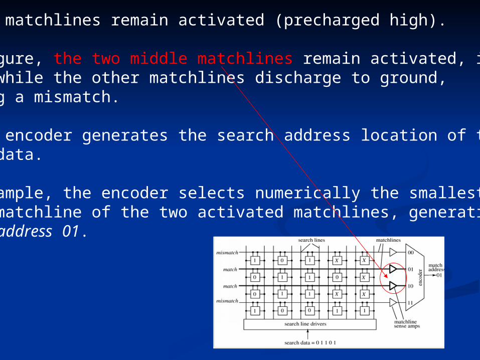
All other matchlines remain activated (precharged high).
In the figure, the two middle matchlines remain activated, indicating a match, while the other matchlines discharge to ground, indicating a mismatch.
Last, the encoder generates the search address location of the matching data. In the example, the encoder selects numerically the smallest numbered matchline of the two activated matchlines, generating the match address 01.

This match address is used as the input address to a RAM that contains a list of output ports as depicted in Figure 2.
This CAM/RAM system is a complete implementation of an address lookup engine.
The match address output of the CAM is in fact a pointer used to retrieve associated data from the RAM.
In this case the associated data is the output port.

Caches memory in microprocessors
The problem: Despite improvements in technology, microprocessors are still much faster than main memory.
Memory access time is increasingly the bottleneck in overall application performance.
As a result, an application might spend a considerable amount of time waiting for data.
This not only negatively impacts the overall performance, but the application cannot benefit much from a processor clock-speed upgrade either.

Solution:
One way to overcome this problem is to insert a small high-speed buffer memory between the processor and main memory.
Such a buffer is generally referred to as cache memory, or cache for short.
In our case the data from the cache is retrieved from the CAMthus instead of translating the data from the processor into anaddress which is associated to a row in the cash, the data fromthe CPU is assigned to a row in the CAM which is associatedto the desired row in the cache. Thus performing quicker.

Translation lookaside buffers (TLB)
The translation lookaside buffer (TLB) is a table in the processor that contains cross-references between the virtual and real addresses of recently referenced pages of memory.
It functions like a "hot list" or quick-lookup index of the pages in main memory that have been most recently accessed.

The problem:
When a cache miss occurs, data must be fetched from an address in virtual memory.
This virtual memory address must be translated into a main memory real address.
If the real-memory address of a desired page is not in the TLB, a further delay is incurred while the real address is determined.

The solution:
Determine the real-memory address of a desired page using CAM.
This will cut down the time of translating the real-memory address of a desired page.
Thus the data will be retrieved faster.


An Important An Important Building- Building-
Block:Block: The Priority The Priority
EncoderEncoder

The Priority EncoderThe Priority Encoder
Priority encoder passes a priority token from a bit Priority encoder passes a priority token from a bit with the highest priority to the bit with the lowest with the highest priority to the bit with the lowest priority.priority.
The function of the The function of the iith output bit of the PE is th output bit of the PE is EPEPi i = D= Dii*P*Pii
where where DDii stands for the corresponding input data stands for the corresponding input data and and PPii stands for the priority token passed into stands for the priority token passed into this bit.this bit.
There’s an iterative relationship between There’s an iterative relationship between PPii and and PPi-i-
11 as as PPi i = ~D= ~Di-1i-1*P*Pi-1i-1 and hence the general expression and hence the general expression
for the output isfor the output is EPEPi i = D= Dii*~D*~Di-1i-1*~D*~Di-2i-2*….*~D*….*~D00

Priority Encoder – cont.Priority Encoder – cont. When constructing a large PE, macros are used. When constructing a large PE, macros are used.
ForFor example, for a 64 bit PE we use 8bit macros. The example, for a 64 bit PE we use 8bit macros. The
8bit 8bit macro itself consists of two 4bit sub-macros. macro itself consists of two 4bit sub-macros. The 4bit sub-macros receive a second-level The 4bit sub-macros receive a second-level
lookahead lookahead signal called LA2.signal called LA2. The 8bit macros receive a third level lookahead The 8bit macros receive a third level lookahead
signalsignal called LA3.called LA3. For the For the iith 8bit macro the functions areth 8bit macro the functions are LA3LA3i i = =
DD8i+78i+7+D+D8i+68i+6+D+D8i+58i+5+D+D8i+48i+4+D+D8i+38i+3+D+D8i+28i+2+D+D8i+18i+1+D+D8i8i
LA2LA2ii = ~(D = ~(D8i+38i+3+D+D8i+28i+2+D+D8i+18i+1+D+D8i8i+LA3+LA3i-1i-1))
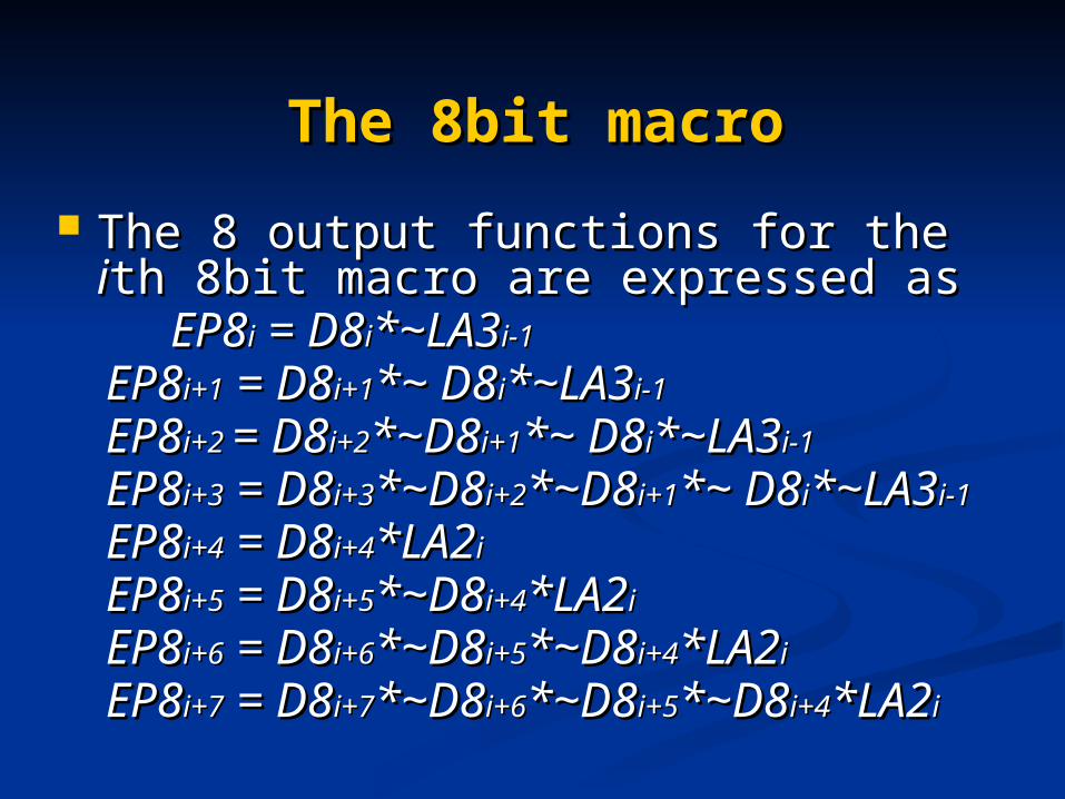
The 8bit macroThe 8bit macro
The 8 output functions for the The 8 output functions for the iith 8bit th 8bit macro are expressed asmacro are expressed as
EP8EP8ii = D8 = D8ii*~LA3*~LA3i-1i-1
EP8EP8i+1i+1 = D8 = D8i+1i+1*~ D8*~ D8ii*~LA3*~LA3i-1i-1
EP8EP8i+2 i+2 = D8= D8i+2i+2*~D8*~D8i+1i+1*~ D8*~ D8ii*~LA3*~LA3i-1i-1
EP8EP8i+3i+3 = D8 = D8i+3i+3*~D8*~D8i+2i+2*~D8*~D8i+1i+1*~ *~ D8D8ii*~LA3*~LA3i-1i-1
EP8EP8i+4i+4 = D8 = D8i+4i+4*LA2*LA2ii
EP8EP8i+5i+5 = D8 = D8i+5i+5*~D8*~D8i+4i+4*LA2*LA2ii
EP8EP8i+6i+6 = D8 = D8i+6i+6*~D8*~D8i+5i+5*~D8*~D8i+4i+4*LA2*LA2ii
EP8EP8i+7i+7 = = D8D8i+7i+7*~D8*~D8i+6i+6*~D8*~D8i+5i+5*~D8*~D8i+4i+4*LA2*LA2ii

Design of the 8bit macroDesign of the 8bit macro We will show a High-Speed Low-Power (HSLP) design for the 8bit macro.We will show a High-Speed Low-Power (HSLP) design for the 8bit macro.
Low-PowerLow-Power consumption is achieved by two means: consumption is achieved by two means:
1. the use of transistors instead of logic gates when implementing functions. 1. the use of transistors instead of logic gates when implementing functions. For example, the function For example, the function D8i+3+D8i+2+D8i+1+D8i+LA3i-1 D8i+3+D8i+2+D8i+1+D8i+LA3i-1 is is implementedimplemented
by connecting 5 transistors’ drains in series, rather than using a 5 inputby connecting 5 transistors’ drains in series, rather than using a 5 inputOR gate.OR gate.
2. In 2. In non LP systemnon LP system, when clock is low, for every i, if Di is low, then EPi, when clock is low, for every i, if Di is low, then EPi goes high. When clock is raised, for every i such that Di is low, EPi is goes high. When clock is raised, for every i such that Di is low, EPi is
pulled pulled down and only for j (j != i) such that Dj is high, EPj remains high.down and only for j (j != i) such that Dj is high, EPj remains high.
The high switching probability results in high power dissipation.The high switching probability results in high power dissipation.In In LP systemsLP systems, when clock is low, for every i EPi remains low. When clock is , when clock is low, for every i EPi remains low. When clock is
raised, for every i such that Di is high, raised, for every i such that Di is high, only oneonly one output bit changes its logic output bit changes its logic level. Hence, there’s a significant reduction in switching activity.level. Hence, there’s a significant reduction in switching activity.
We note that there’s a conceptual similarity between this case and the We note that there’s a conceptual similarity between this case and the considerations regarding the Pmos dominated design of the CAM core cell.considerations regarding the Pmos dominated design of the CAM core cell.
High-SpeedHigh-Speed characteristic is achieved through the use of multilevel characteristic is achieved through the use of multilevel
lookahead structure: A level does not have to operate if a higher prioritylookahead structure: A level does not have to operate if a higher prioritylevel does.level does.
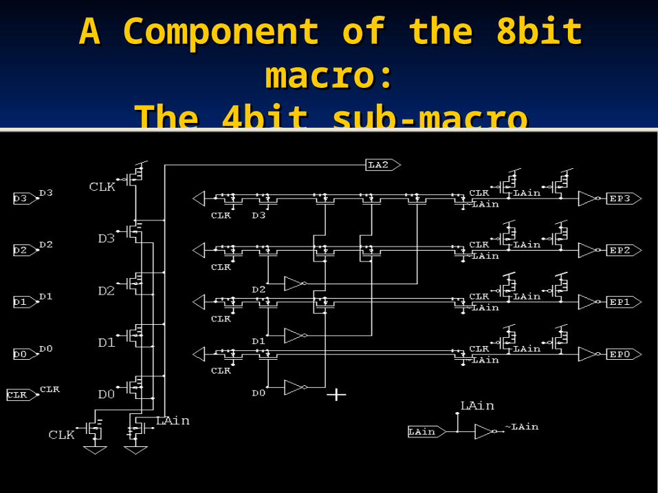
A Component of the 8bit A Component of the 8bit macro:macro:
The 4bit sub-macroThe 4bit sub-macro

4bit sub-macro Simulation4bit sub-macro Simulation
The EP0 output is high whenever the corresponding input (D0) is
high and clock is high too

4bit sub-macro Simulation 4bit sub-macro Simulation (cont.)(cont.)
This time, the output EP1 is high
depending on the input D1, the clock
AND on the fact that no higher priority is
turned on!

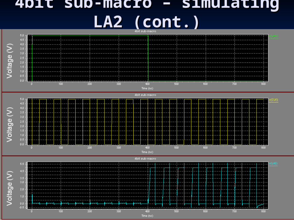
4bit sub-macro – 4bit sub-macro – simulating LA2simulating LA2
Why do we get These invalid values instead of Zero???

4bit sub-macro – simulating 4bit sub-macro – simulating LA2 (cont.)LA2 (cont.)
Why did we get these invalid values?Why did we get these invalid values? The following equation must be held: The following equation must be held:
The width is equal for all Nmos transistors, The width is equal for all Nmos transistors, but their length must be summed. We must but their length must be summed. We must also calculate the distances between the also calculate the distances between the transistors. We have calculated that the transistors. We have calculated that the total length should be 20Ln. Hence we get total length should be 20Ln. Hence we get the relation 0.25*Wn = Wp. Only by having the relation 0.25*Wn = Wp. Only by having this relation, the invalid values disappear.this relation, the invalid values disappear.
* * pnn p
n p
ww
l l
4bit sub-macro – simulating 4bit sub-macro – simulating LA2 (cont.)LA2 (cont.)

8bitmacro

8bit macro Simulation8bit macro Simulationimportant note: the width in the following simulations looks very important note: the width in the following simulations looks very narrow, but in fact the units are in micro seconds (not in nano secs). narrow, but in fact the units are in micro seconds (not in nano secs). The reason for that is that we wanted to cover all 256 cases (since we The reason for that is that we wanted to cover all 256 cases (since we have 8 inputs) so in order to show them all in the same graph, the have 8 inputs) so in order to show them all in the same graph, the widths are relatively narrow. This is just for logical purposes and not widths are relatively narrow. This is just for logical purposes and not functional purposes.functional purposes.
Plots of the first 4 outputs (EP0 to EP3)
as function of all 8 inputs (D0 to D7)

8bit macro Simulation 8bit macro Simulation (cont.)(cont.)
Plots of the last 4 outputs (EP4 to EP7)as function of all 8 inputs (D0 to D7)

Longer Priority EncodersLonger Priority Encoders Consider a 64 bit PE. We will Consider a 64 bit PE. We will
connect eight 8bit macros.connect eight 8bit macros. Since the critical path has Since the critical path has
dramatically increased, a severe dramatically increased, a severe problem occurred and invalid values problem occurred and invalid values appeared.appeared.
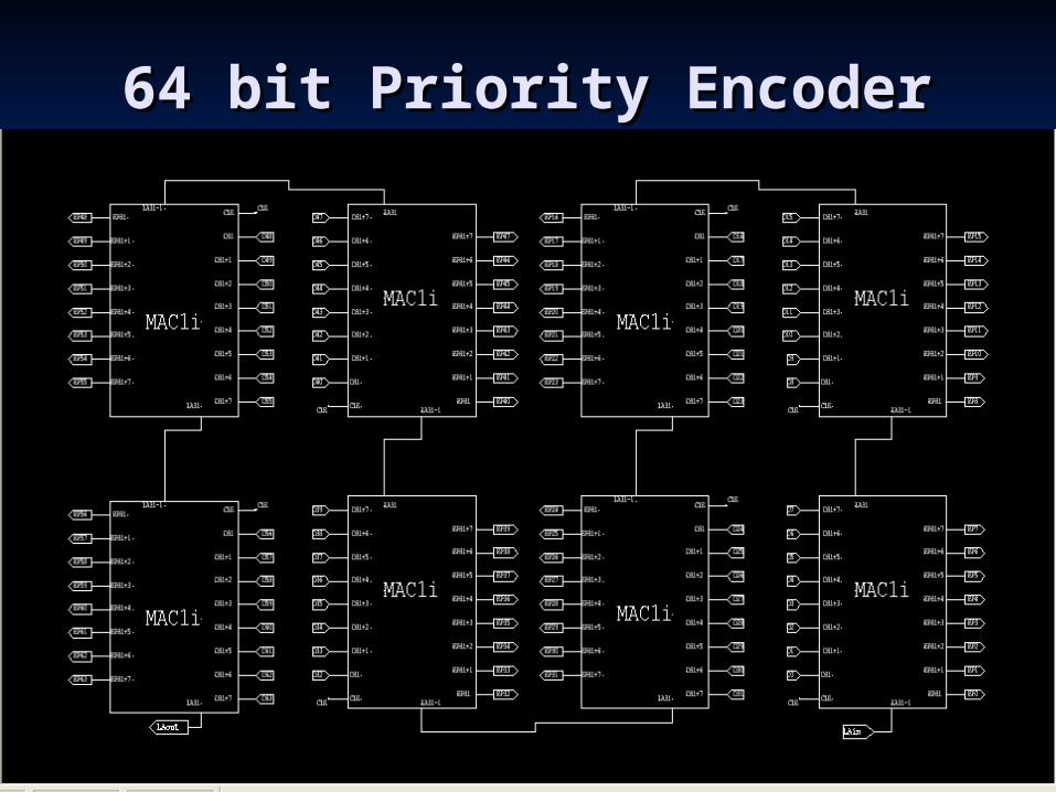
64 bit Priority Encoder64 bit Priority Encoder

64bit Simulation64bit SimulationInvalid values: when D4 is high, no matter what is the value of any higher input
(e.g. D23), the output of the corresponding output (EP23) should be low, but here we
see undesired peaks!

64bit simulation – 64bit simulation – analysis analysis
Our solution: decrease the rise-time and fall-time of the Our solution: decrease the rise-time and fall-time of the clock, increase the high level of the clock and decrease clock, increase the high level of the clock and decrease its low level period - though it’s its low level period - though it’s not a good solutionnot a good solution since it’s hard to create since it’s hard to create anti-symmetricanti-symmetric signals. signals.
In T-Spice, instead of:In T-Spice, instead of: CLK Gnd pulse (0 5 0 .5n .5n 10n 20n)CLK Gnd pulse (0 5 0 .5n .5n 10n 20n) we have:we have: CLK Gnd pulse (5 0 0 .1n .1n 2n 10n)CLK Gnd pulse (5 0 0 .1n .1n 2n 10n) But there’s a better solution, independent of rise-times, But there’s a better solution, independent of rise-times,
fall-times and pulse widths.fall-times and pulse widths. It’s called folding.It’s called folding.

64bit Simulation – cont.64bit Simulation – cont.The undesired
peaks disappearedThrough changing
the clock

Folding Technique in Folding Technique in Long Long
Priority Encoders Priority Encoders In the previous configuration, the LAout In the previous configuration, the LAout
was connected to the neighboring 8bit was connected to the neighboring 8bit macro. Actually, this output can be macro. Actually, this output can be connected to all the other macros with connected to all the other macros with lower priority. Such extra connections can lower priority. Such extra connections can shorten the critical path and hence reduce shorten the critical path and hence reduce the propagation delay. This technique is the propagation delay. This technique is called first-level folding. In our encoder called first-level folding. In our encoder we will use only the first-level folding, but we will use only the first-level folding, but other levels of folding exist too.other levels of folding exist too.

Realization of 64bit PE Realization of 64bit PE using the using the first-level first-level
folding techniquefolding technique
A design as a 2-dimensional array with folding. Macro0 is connected to Macro1 and macro3; macro2 is connected to macro3 and macro5; macro4 is connected to macro5 and macro7. The rest of the macros are connected regularly – the ith macro is connected to the i+1th macro.
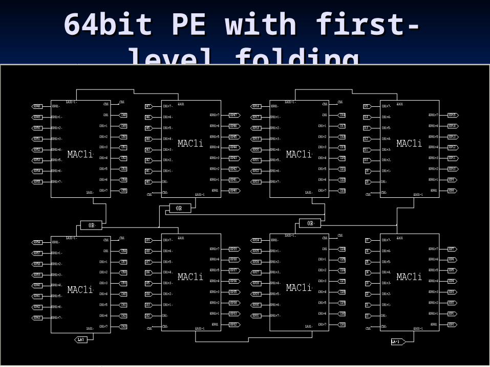
64bit PE with first-level 64bit PE with first-level foldingfolding

Simulation of 64bit with Simulation of 64bit with foldingfolding
The peaks disappeared
due to the use of folding

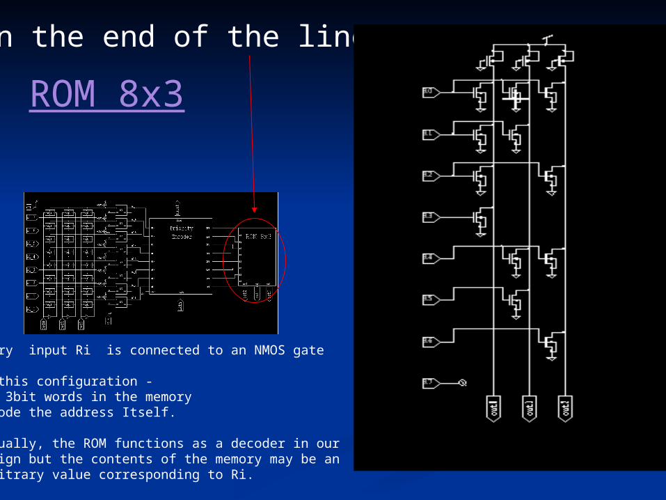
In the end of the line…
Every input Ri is connected to an NMOS gate
In this configuration -the 3bit words in the memory encode the address Itself.
Actually, the ROM functions as a decoder in our Design but the contents of the memory may be an arbitrary value corresponding to Ri.
ROM 8x3
R0R0 R1R1 R2R2 R3R3 R4R4 R5R5 R6R6 R7R7
11 00 00 00 00 00 00 00
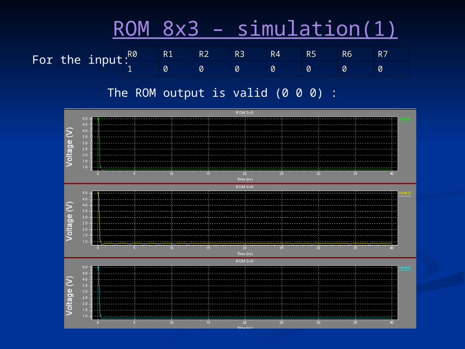
ROM 8x3 – simulation(1)For the input:
The ROM output is valid (0 0 0) :

R0R0 R1R1 R2R2 R3R3 R4R4 R5R5 R6R6 R7R7
00 00 00 11 00 00 00 00For the input:
The ROM output is valid (0 1 1) :
ROM 8x3 – simulation(2)
R0R0 R1R1 R2R2 R3R3 R4R4 R5R5 R6R6 R7R7
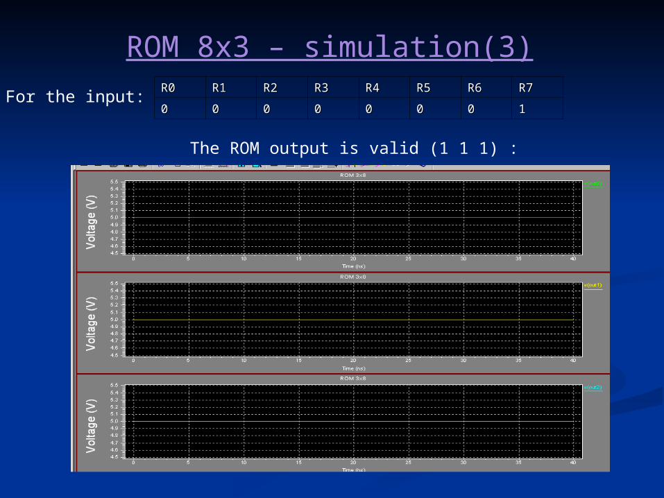
00 00 00 00 00 00 00 11For the input:
The ROM output is valid (1 1 1) :
ROM 8x3 – simulation(3)

wl_0
wl_1
wl_2
wl_3
wl_4
wl_5
wl_6
wl_7
ml_7
ml_6
ml_5
ml_4
ml_3
ml_2
ml_1
ml_0
ron
clk
clk
clk
clk
ref2
ref1
ref0
clk
clk
clk
clk
clk
clk
ch
ch
ch
ch
ch
ch
ch
ch
ch
ch
CLK
DDff
Q
Qnot
CLK
D
DffQ
Qnot
CLK
DDff
Q
Qnot
CLK
D
DffQ
Qnot
CLK
D
DffQ
Qnot
CLK
DDff
Q
Qnot
CLK
D
DffQ
Qnot
CLK
DDff
Q
Qnot
bcellml
wl~bbcell
ml
wl~bb cell
ml
wl~b
bcellml
wl~bbcell
ml
wl~bb cell
ml
wl~b
bcellml
wl~bbcell
ml
wl~bb cell
ml
wl~b
bcellml
wl~bbcell
ml
wl~bb cell
ml
wl~b
bcellml
wl~bbcell
ml
wl~bb cell
ml
wl~b
bcellml
wl~bbcell
ml
wl~bb cell
ml
wl~b
bcellml
wl~bbcell
ml
wl~bb cell
ml
wl~b
bcellml
wl~bbcell
ml
wl~bb cell
ml
wl~b
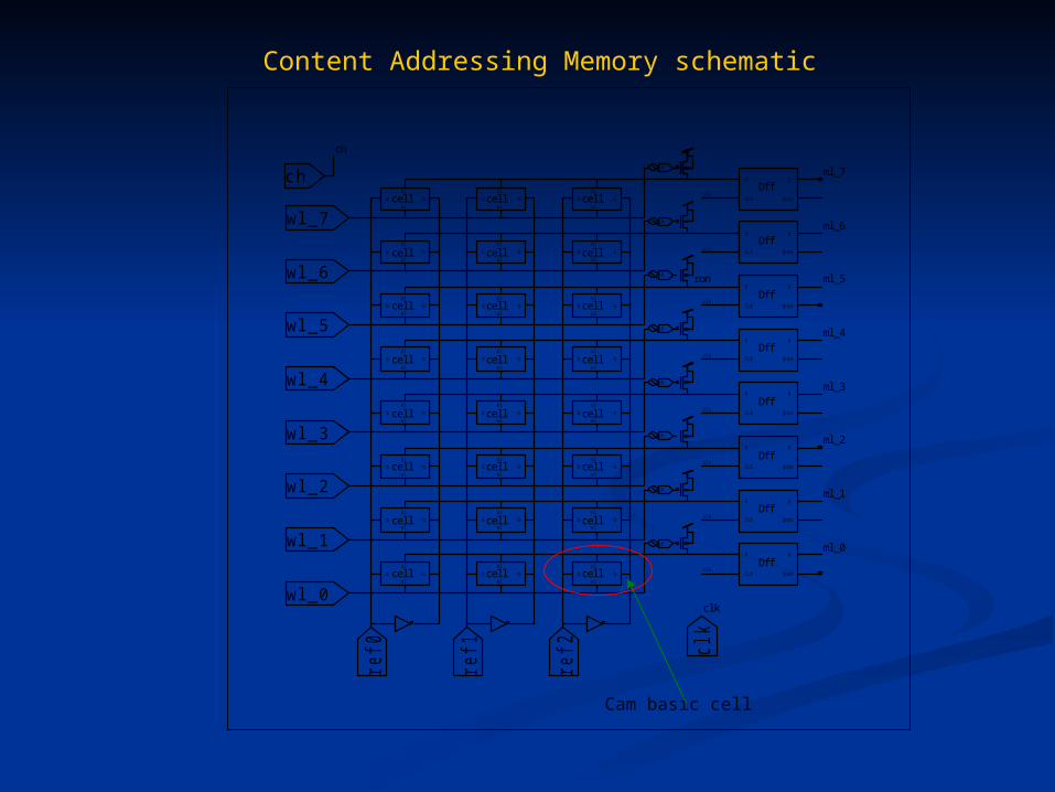
Content Addressing Memory schematic
Cam basic cell

CAM basic cell interface
inputs: reference bit (b) internal memory : stored data bit (d) word line: enabling write operation to the cell (wl) output: match line, indicates if there was a match (ml)
The CAM basic cell is made out of 2 basic parts:
1) SRAM 1bit Memory unit
2) Comparison unit
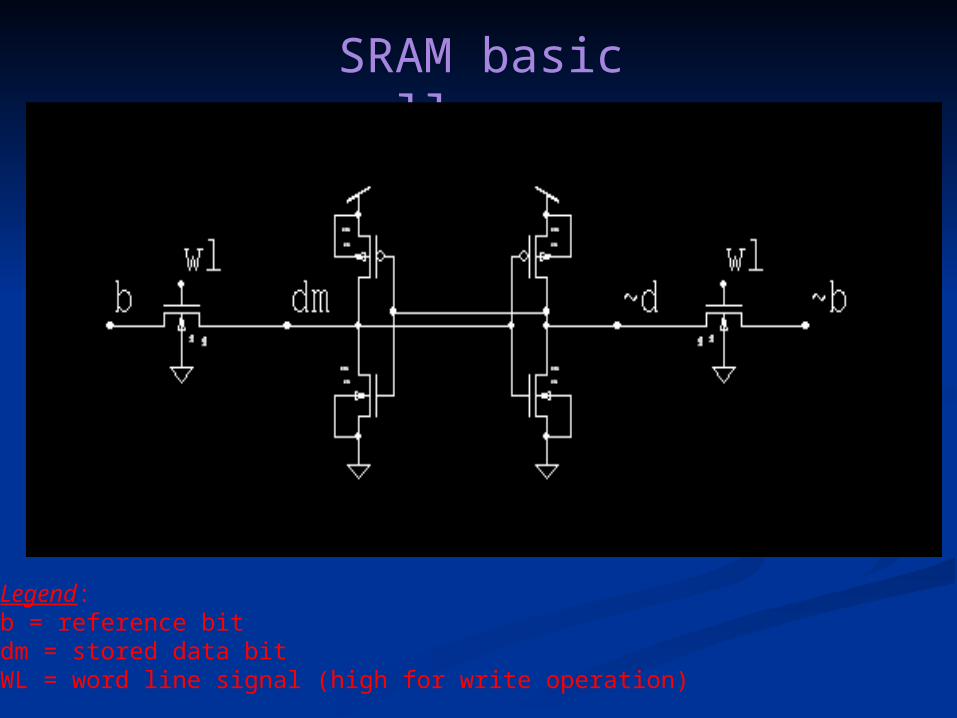
SRAM basic cell
Legend: b = reference bit dm = stored data bit WL = word line signal (high for write operation)

SRAM simulation
WL High for write
operation
Reference bit
Data bit
The reference is stored on a write operation and the data is stable when WL is logical ‘0’
Data bit_not

CAM core cell – design 1
Consists of an SRAM basic cell and a comparison unit.The comparison unit calculates the logical EX-NOR operation

CAM core cell – design 2In this design we use a comparison unit which is built of 3 transistors Instead of 4 transistors in the previous design.Because the cell is the basic component of our system we decided toexamine both designs. The match line must be precharged to high level.

CAM core cell – design 2 – PMOS dominated
This implementation is complementary to the one we choseIt similar conceptually, but here the match line must be discharged to a low level.

match occurrences are rare, therefore it is better if the transitions take place only in matches,in the common designs we have found in references the transitions take place in mismatches.
In this design the match line is pre-discharged, and a pull-up takes place on a match
CAM core cell – design 3

Match configuration

Mismatch configuration

Bad “1”On a match
Reference bit
Data bit
Word line
CAM core cell simulationIn case of a mismatch on a search cycle we get a good “0” but not a good “1” for a match.This is due to the fact that when pull-up occur the maximal “1” that appear is Vcc-Vt.Therefore a PMOS circuit must be added for precharging the match line.

CAM core cell with PrechargeAchieving good “1” on a match is possible only if a precharge unit is added.In the NMOS dominated design the match line must be precharged to high level
Precharge unit added to the design

CAM core cell with Precharge - simulation
good “1”On a match
Reference bit
Data bit
Word line
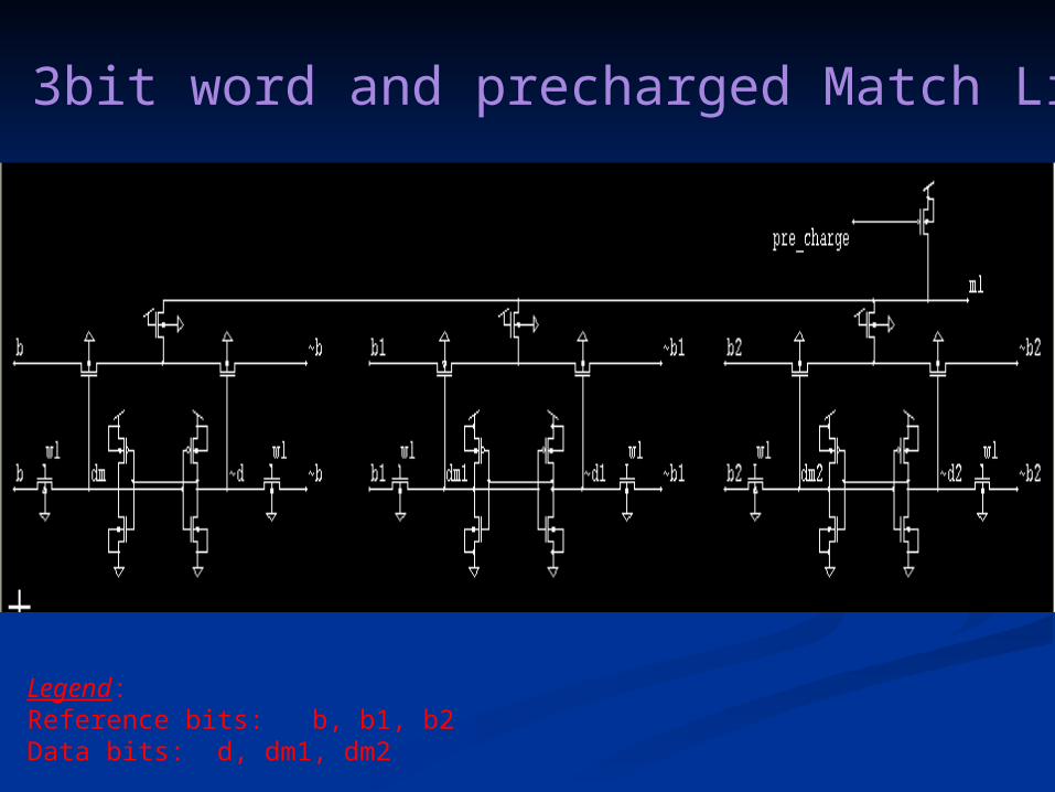
CAM 3bit word and precharged Match Line
Legend:Reference bits: b, b1, b2Data bits: d, dm1, dm2

On a search operation the match line voltage is affected by the comparison between the reference bit and the stored data bit.
In the following simulation 3 mismatch cases have been tested:1) Mismatch in all 3 cells2) Mismatch in only 2 cells 3) Mismatch in only 1 cell
The performance deteriorates as we go through these cases because
if a mismatch is detected in any one of the cells, a pull down takes place
by the NMOSs which connects the match line to the relevant cell.
Ideally, the match line must be pulled down to low voltage even if a pull
Down takes place in only one NMOS, but we still get bad “0” for cases
2 and 3. This happens because the high voltage precharge circuit is
Not totally discharged.
CAM word search simulation

Cam 3bit word case1: b!=dm, b1!=dm1, b2!=dm2.

Cam 3bit word case1: b!=dm, b1!=dm1, b2!=dm2. let’s take a close look at ml

Cam 3bit word case 2: b = dm, b1!=dm1, b2!=dm2.
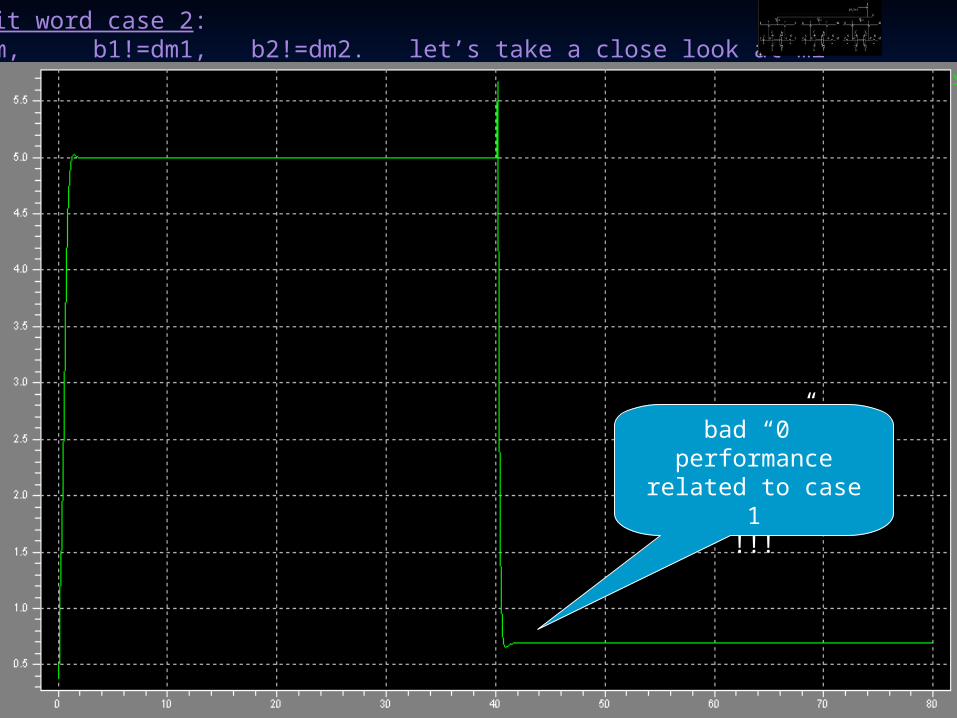
bad “0” performancerelated to case 1
!!!
Cam 3bit word case 2: b = dm, b1!=dm1, b2!=dm2. let’s take a close look at ml

Cam 3bit word case 3:b =dm, b1 = dm1, b2!=dm2.
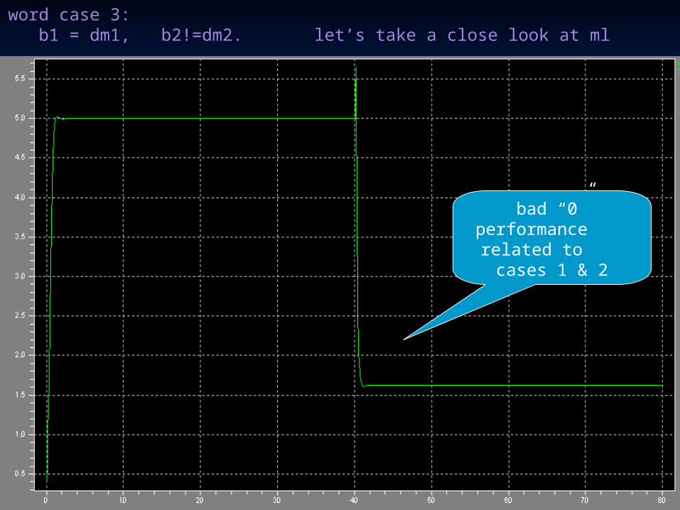
Cam 3bit word case 3: b =dm, b1 = dm1, b2!=dm2. let’s take a close look at ml
bad “0” performance related to cases 1 & 2
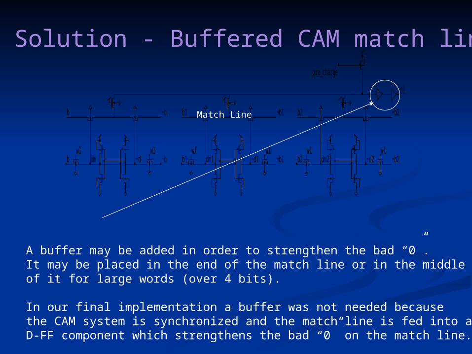
Solution - Buffered CAM match line
A buffer may be added in order to strengthen the bad “0”. It may be placed in the end of the match line or in the middleof it for large words (over 4 bits).
In our final implementation a buffer was not needed becausethe CAM system is synchronized and the match line is fed into aD-FF component which strengthens the bad “0” on the match line.
b
b
~b
~bwlwl
~ddm
pre_charge
b1
b1
~b1
~b1wlwl
~d1dm1
b2
b2
~b2
~b2wlwl
~d2dm2
ml
Match Line

Buffered CAM Match line – simulation
For case 3The match line is pulled down with
Good “0”

CAM word simulationA problem we encountered –The match line remains on high voltage for a mismatch when clock cycle chosen is 4ns
Mismatch
Reference bit
Data bit stored in CAM
Match line highfor the mismatch!

CAM word simulation – resolution
the clock must be configured to a longer clock cycle
the low voltage portion of the clock cycle may be shortened
the clock and the word line signal must be synchronized correctly. When a pull down occurres in the word line the clock must be set to High, otherwise a further delay will take place.
The root of the problem is the delay inherent to the system and mostly on the setup time of the D-FF on the match line end.
In order to prevent ill conditioning as described in the previous slide Changes may be applied to the clock configuration :
Another possibility – regress our design to the 4-transistor implementation ! The comparison unit is designed better for the pull down !

Delay 1: match line propagation
Delay 2: D-FF setup time
Match line before D-FF
Match line after D-FF
Reference bit
Stored data bit
word line signal
Clock
In order to resolve the problem we have set the clock cycle to 10ns.
MLPulldown

Match line before D-FF
Match line after D-FF
Reference bit
Stored data bit
word line signal
Clock
For propagation delay reduction we synchronized the clock withThe word line signal and set the high level to a longer period
ML

8 3bit word CAM implementation
Due to problems encountered previously we have decided toimplement our system with the 4-transistor comparison mechanism,
Our main consideration was the ill conditioning in the case of 1-bitmismatch. The 4-transistor unit includes an active pull down, this enables us to be more flexible in the choice of clock cycle and prechargesynchronization.
wl_0
wl_1
wl_2
wl_3
wl_4
wl_5
wl_6
wl_7
ml_7
ml_6
ml_5
ml_4
ml_3
ml_2
ml_1
ml_0
ron
clk
clk
clk
clk
ref2
ref1
ref0
clk
clk
clk
clk
clk
clk
ch
ch
ch
ch
ch
ch
ch
ch
ch
ch
CLK
DDff
Q
Qnot
CLK
D
DffQ
Qnot
CLK
DDff
Q
Qnot
CLK
D
DffQ
Qnot
CLK
D
DffQ
Qnot
CLK
DDff
Q
Qnot
CLK
D
DffQ
Qnot
CLK
DDff
Q
Qnot
bcellml
wl~bbcell
ml
wl~bb cell
ml
wl~b
bcellml
wl~bbcell
ml
wl~bb cell
ml
wl~b
bcellml
wl~bbcell
ml
wl~bb cell
ml
wl~b
bcellml
wl~bbcell
ml
wl~bb cell
ml
wl~b
bcellml
wl~bbcell
ml
wl~bb cell
ml
wl~b
bcellml
wl~bbcell
ml
wl~bb cell
ml
wl~b
bcellml
wl~bbcell
ml
wl~bb cell
ml
wl~b
bcellml
wl~bbcell
ml
wl~bb cell
ml
wl~b

WL(i)
PRECHARGE
REF(i)
SRAM
DATA
ML(i)
CLK
LAout
OUT(i)
CHARGE
REFERENCE WRITE BIT
STORED DATA BIT
MATCH \ MISMATCH
LAout OF PE SERVES AS VALID BIT {IN CASE OF A MATCH WILL BE HIGH}
X XXPRECHARGE IN PE ENABLES ONLY IN HIGH CLK LEVEL
9ns
10ns
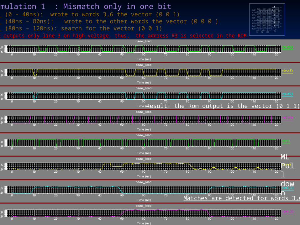
CAM Simulation 1 : Mismatch only in one bit Stage 1: (0 - 40ns): wrote to words 3,6 the vector (0 0 1) Stage 2: (40ns – 80ns): wrote to the other words the vector (0 0 0 )Stage 3: (80ns – 120ns): search for the vector (0 0 1) the PE outputs only line 3 on high voltage, thus, the address R3 is selected in the ROM.
Matches are detected for words 3,6
Result: the Rom output is the vector (0 1 1)
MLPulldown
ml_0
clk
clk
clk
clk
clk
clk
clk
clk
wl_0
wl_1
wl_2
wl_3
wl_4
wl_5
wl_6
ref2
ref1
wl_7
ref0
clk
ml_1
ml_2
ml_3
ml_4
ml_5
ml_6
ml_7
clk
CLK
DDff
Q
Qnot
CLK
DDff
Q
Qnot
CLK
DDff
Q
Qnot
CLK
D
DffQ
Qnot
CLK
D
DffQ
Qnot
CLK
DDff
Q
Qnot
CLK
DDff
Q
Qnot
CLK
DDff
Q
Qnotbcellml
wl~bb cell
ml
wl~b bcell
ml
wl~b
bcellml
wl~bb cell
ml
wl~b bcell
ml
wl~b
bcellml
wl~bb cell
ml
wl~b bcell
ml
wl~b
bcellml
wl~bb cell
ml
wl~b bcell
ml
wl~b
bcellml
wl~bb cell
ml
wl~b bcell
ml
wl~b
bcellml
wl~bb cell
ml
wl~b bcell
ml
wl~b
bcellml
wl~bb cell
ml
wl~b bcell
ml
wl~b
bcellml
wl~bbcell
ml
wl~bb cell
ml
wl~b

CAM simulation 2 : Mismatch in 2 bitsStage 1: (0 - 40ns): wrote to words 3,6 the vector (1 0 1) Stage 2: (40ns – 80ns): wrote to the other words the vector (0 0 0 )Stage 3: (80ns – 120ns): search for the vector (1 0 1) the PE outputs only line 3 on high voltage, thus, the address R3 is selected in the ROM.
Result: the Rom output is the vector (0 1 1)
ml_0
clk
clk
clk
clk
clk
clk
clk
clk
wl_0
wl_1
wl_2
wl_3
wl_4
wl_5
wl_6
ref2
ref1
wl_7
ref0
clk
ml_1
ml_2
ml_3
ml_4
ml_5
ml_6
ml_7
clk
CLK
DDff
Q
Qnot
CLK
DDff
Q
Qnot
CLK
DDff
Q
Qnot
CLK
D
DffQ
Qnot
CLK
D
DffQ
Qnot
CLK
DDff
Q
Qnot
CLK
DDff
Q
Qnot
CLK
DDff
Q
Qnotbcellml
wl~bb cell
ml
wl~b bcell
ml
wl~b
bcellml
wl~bb cell
ml
wl~b bcell
ml
wl~b
bcellml
wl~bb cell
ml
wl~b bcell
ml
wl~b
bcellml
wl~bb cell
ml
wl~b bcell
ml
wl~b
bcellml
wl~bb cell
ml
wl~b bcell
ml
wl~b
bcellml
wl~bb cell
ml
wl~b bcell
ml
wl~b
bcellml
wl~bb cell
ml
wl~b bcell
ml
wl~b
bcellml
wl~bbcell
ml
wl~bb cell
ml
wl~b
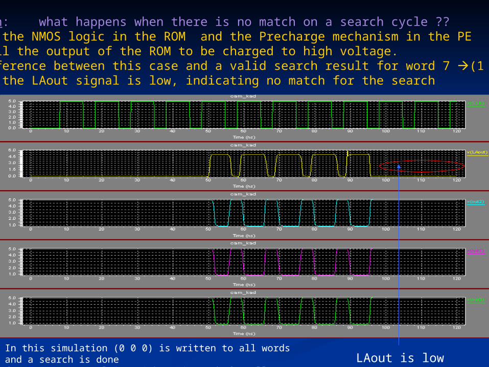
Question: what happens when there is no match on a search cycle ??Answer: the NMOS logic in the ROM and the Precharge mechanism in the PEcause all the output of the ROM to be charged to high voltage.The difference between this case and a valid search result for word 7 (1 1 1) is that the LAout signal is low, indicating no match for the search
LAout is low In this simulation (0 0 0) is written to all words and a search is donefor (1 0 1), resulting with a mismatch for all words.

For a match on word 7 –if all the other words are in mismatch, the ROM outputis the same but LAout is high


ROM 8x3 (logic)

ROM 8x3 (chip)ROM 8x3 (chip)
R6
Vdd
R1
R2 out2 out1
out0
Gnd
R5
R7R3 R4
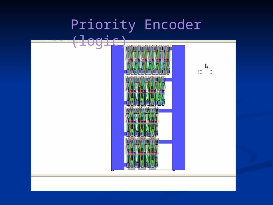
Priority Encoder (logic)

Priority Encoder (chip)Priority Encoder (chip)
LAout
EP7
VddEP6
EP5
EP4
LAin CLK D5 D6 D7
EP3 EP2 EP1 EP0 D0
D4
D3
Gnd
D2
D1

CAM (logic)

CAM + PE +ROM (logic)

CAM + PE + ROM (chip)CAM + PE + ROM (chip)
Wl_5
Wl_6
Vdd
Wl_4
Wl_3
out1 out0 out2 ref1
Wl_2 Wl_1 Wl_0 ref0
ref2
charge
Gnd
CLK
Wl_7


% *******************************************************************************% JOB FINDER SYSTEM - IMPLEMNTED WITH CONTENT ADDRESSING MEMORY% *******************************************************************************% This file includes an implementation of a job assignment system% which provides as output the student's name given as input a job code.% the system is initialized by encoding each student, the code is determined % by the profession of the student (skill criterion), and the priority by the % grade average (quality criterion).%% Example:% -------------% the code for a Data Bases designer is 010
% SHAY AGASI and SIVAN CARMEL took the course "Introduction to Data Bases theory"% therefore the code responding to their names is 101 according to the % skill criterion.% we know that Tom has a 91.8 average while Bill has an average of 91.5% therefore Tom has a higher priority. % our configured students and their corresponding skill codes are:
% Student name Student skills % -------------------- -------------------------------------- % ROM(0) = 'ALON COHEN' % -100 (DSP programmer)% ROM(1) = 'SHAY AGASI' % -010 (Data Base designer) -% ROM(2) = 'BILL NOISE' % -110 (VLSI Designer)% ROM(3) = 'SHOSHAN TIBNY ' % -110 (VLSI Designer) % ROM(4) = 'NETA TAYLOR ' % -110 (VLSI Designer) % ROM(5) = 'MOSHE LOPIAN' % -100 (DSP programmer) % ROM(6) = 'YEHUDA ADLER' % -110 (VLSI Designer) % ROM(7) = 'SIVAN CARMEL' % -010 (Data Base designer)
% Shay has a 91.5 average and Sivan has a 91.8 average % therefore Sivan gets higher priority.

clearROM = { 'ALON COHEN' , 'SHAY AGASI' , 'BILL NOISE' , 'SHOSHAN TIBNY ' , ... 'NETA TAYLOR ' , 'MOSHE LOPIAN' , 'YEHUDA ADLER' , 'SIVAN CARMEL' };SRAM = zeros(8,3); %**************** SRAM job code Initialization***********************%function [SRAM,match] = CAM(ref,wl,mask,reset,SRAM)[SRAM,match] = CAM( [1 0 0] , [1 0 0 0 0 0 0 0] , [0 0 0] , 0 ,SRAM );[SRAM,match] = CAM( [0 1 0] , [0 1 0 0 0 0 0 0] , [0 0 0] , 0 ,SRAM );[SRAM,match] = CAM( [1 1 0] , [0 0 1 0 0 0 0 0] , [0 0 0] , 0 ,SRAM );[SRAM,match] = CAM( [1 1 0] , [0 0 0 1 0 0 0 0] , [0 0 0] , 0 ,SRAM );[SRAM,match] = CAM( [1 1 0] , [0 0 0 0 1 0 0 0] , [0 0 0] , 0 ,SRAM );[SRAM,match] = CAM( [1 0 0] , [0 0 0 0 0 1 0 0] , [0 0 0] , 0 ,SRAM );[SRAM,match] = CAM( [1 1 0] , [0 0 0 0 0 0 1 0] , [0 0 0] , 0 ,SRAM );[SRAM,match] = CAM( [0 1 0] , [0 0 0 0 0 0 0 1] , [0 0 0] , 0 ,SRAM );
Output:
SRAM =
1 0 0 0 1 0 1 1 0 1 1 0 1 1 0 1 0 0 1 1 0 0 1 0

%*********** Upon availability of a Data Base designer job **********% ********** a search is done in order to find students with ********** % ********** skills for the job *********************************************** [SRAM,match] = CAM( [0 1 0] , [0 0 0 0 0 0 0 0] , [0 0 0] , 0 ,SRAM ); %************************************************************************* %*** Priority encoding of the match line *********************** for n = 1:8 if match(n) == 1 ind = n; endend
ROM(ind);
SRAM =
1 0 0 0 1 0 1 1 0 1 1 0 1 1 0 1 0 0 1 1 0 0 1 0
match =
0 1 0 0 0 0 0 1
ans =
'SIVAN CARMEL'
Output:
% Student name Student skills % -------------------- -------------------------------------- % ROM(0) = 'ALON COHEN' % -100 (DSP programmer)% ROM(1) = 'SHAY AGASI' % -010 (Data Base designer) -% ROM(2) = 'BILL NOISE' % -110 (VLSI Designer)% ROM(3) = 'SHOSHAN TIBNY ' % -110 (VLSI Designer) % ROM(4) = 'NETA TAYLOR ' % -110 (VLSI Designer) % ROM(5) = 'MOSHE LOPIAN' % -100 (DSP programmer) % ROM(6) = 'YEHUDA ADLER' % -110 (VLSI Designer) % ROM(7) = 'SIVAN CARMEL' % -010 (Data Base designer)
ROM CONFIGURATION

% ********* Upon availability of a Data Base designer job%********** or a VLSI designer job a search is done for the% ********** job code "X10" where X denotes "don't care" therefore% ********** the MSB reference bit may be masked.%*********** therefore we chose the mask vector to be [1 0 0][SRAM,match] = CAM( [0 1 0] , [0 0 0 0 0 0 0 0] , [1 0 0] , 0 ,SRAM );%************************************************************************* %*** Priority encoding of the match line *********************** for n = 1:8 if match(n) == 1 ind = n; endend
ROM(ind)
Output: SRAM =
1 0 0 0 1 0 1 1 0 1 1 0 1 1 0 1 0 0 1 1 0 0 1 0
match =
0 1 1 1 1 0 1 1
ans =
'SIVAN CARMEL'
% Student name Student skills % -------------------- -------------------------------------- % ROM(0) = 'ALON COHEN' % -100 (DSP programmer)% ROM(1) = 'SHAY AGASI' % -010 (Data Base designer) -% ROM(2) = 'BILL NOISE' % -110 (VLSI Designer)% ROM(3) = 'SHOSHAN TIBNY ' % -110 (VLSI Designer) % ROM(4) = 'NETA TAYLOR ' % -110 (VLSI Designer) % ROM(5) = 'MOSHE LOPIAN' % -100 (DSP programmer) % ROM(6) = 'YEHUDA ADLER' % -110 (VLSI Designer) % ROM(7) = 'SIVAN CARMEL' % -010 (Data Base designer)
ROM CONFIGURATION

% ********* Upon availability of a DSP Programmer job%********** or a VLSI designer job a search is done for the% ********** job code "1X1" where X denotes "don't care" therefore% ********** the MSB reference bit may be masked.%*********** therefore we chose the mask vector to be [1 X 1] [SRAM,match] = CAM( [1 0 0] , [0 0 0 0 0 0 0 0] , [0 1 0] , 0 ,SRAM ); %************************************************************************* %*** Priority encoding of the match line *********************** for n = 1:8 if match(n) == 1 ind = n; endend
ROM(ind);
SRAM =
1 0 0 0 1 0 1 1 0 1 1 0 1 1 0 1 0 0 1 1 0 0 1 0
match =
1 0 1 1 1 1 1 0
ans =
'YEHUDA ADLER'
Output: % Student name Student skills % -------------------- -------------------------------------- % ROM(0) = 'ALON COHEN' % -100 (DSP programmer)% ROM(1) = 'SHAY AGASI' % -010 (Data Base designer) -% ROM(2) = 'BILL NOISE' % -110 (VLSI Designer)% ROM(3) = 'SHOSHAN TIBNY ' % -110 (VLSI Designer) % ROM(4) = 'NETA TAYLOR ' % -110 (VLSI Designer) % ROM(5) = 'MOSHE LOPIAN' % -100 (DSP programmer) % ROM(6) = 'YEHUDA ADLER' % -110 (VLSI Designer) % ROM(7) = 'SIVAN CARMEL' % -010 (Data Base designer)
ROM CONFIGURATION

%*****************************************************************% This file includes an implementation for a Content addressing% memory, for a reference input a match is detected in the memory% the word line bit (wl) indicates a write operation is taking place.% our hardware implementation propagates the results to the match line% requiring O(1) time complexity.
function [SRAM,match] = CAM(ref,wl,mask,reset,SRAM);
% writefor n = 1:8 if wl(n) == 1 for m = 1:3 SRAM(n,m)=ref(m); end end end %search - in hardware implementation this takes O(1) for n = 1:8 match(n) = 1; for m = 1:3 if mask(m) == 0 if wl(n) == 0 if SRAM(n,m) ~= ref(m); match(n) = 0; end end end end end


![[ Moshe Mishali and Yonina C. Eldar ]](https://img.pdfslide.us/doc/110x75/61c4cb8c10e9a8212d491b39/-moshe-mishali-and-yonina-c-eldar-.jpg)


