Embed Size (px)
Citation preview

MOSFET SPICE model grade
Application Note
2021-06-21
1 © 2021 Toshiba Electronic Devices & Storage Corporation
Overview
This section presents the grades of MOSFET SPICE models we provide, and compares the calculated results of
these models with the characteristic curves of the data sheet. Referring to this application note, please select the most
suitable model grade for the simulation environment and purpose.
MOSFET SPICE model grade

MOSFET SPICE model grade
Application Note
2021-06-21
2 © 2021 Toshiba Electronic Devices & Storage Corporation
Table of contents
Overview ................................................................................................................................................................. 1
1. Introduction ......................................................................................................................................................... 4
2. Definition of model name and model grade ....................................................................................................... 4
2.1. Model name ......................................................................................................................................................... 4
2.2. Encryption ............................................................................................................................................................ 4
2.3. Definition of model grades G0 and G2 ................................................................................................................ 5
3. Fitting accuracy (RMS error) .............................................................................................................................. 6
4. Fitting accuracy comparison of G0 and G2 model in U-MOS series ...................................................................
4.1 ID-VDS curve (TPH5R60APL)............................................................................................................................... 7
4.2 Parasitic capacitance curve (TPH5R60APL) ........................................................................................................ 8
4.3 Switching Analysis (TPH1R306PL) ..................................................................................................................... 9
5. Fitting accuracy comparison of G0 and G2 model in DTMOS series .............................................................. 11
5.1 ID-VDS curve (TK040N65Z) ................................................................................................................................ 11
5.2 Parasitic capacitance curve (TK040N65Z) ......................................................................................................... 12
5.3 Switching Analysis (TK040N65Z) ..................................................................................................................... 13
RESTRICTIONS ON PRODUCT USE ............................................................................................................... 15
MOSFET SPICE model grade
Application Note
2021-06-21
3 © 2021 Toshiba Electronic Devices & Storage Corporation
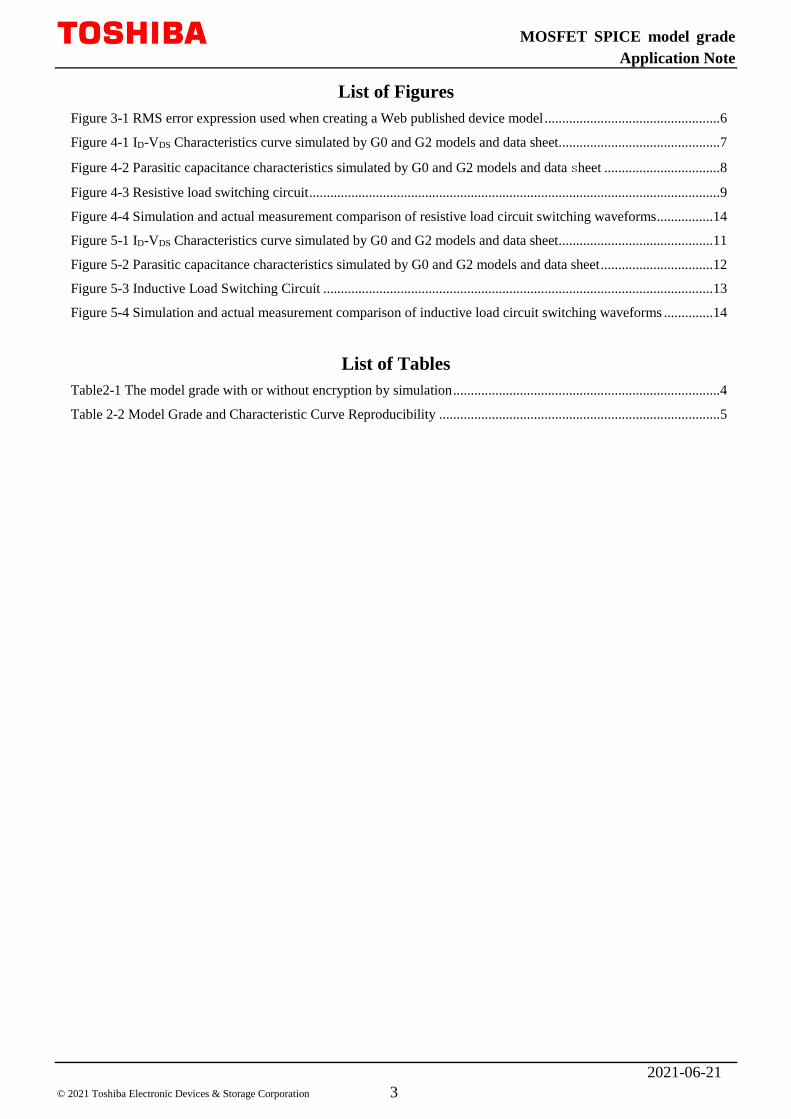
List of Figures
Figure 3-1 RMS error expression used when creating a Web published device model .................................................. 6
Figure 4-1 ID-VDS Characteristics curve simulated by G0 and G2 models and data sheet .............................................. 7
Figure 4-2 Parasitic capacitance characteristics simulated by G0 and G2 models and data sheet ................................. 8
Figure 4-3 Resistive load switching circuit ..................................................................................................................... 9
Figure 4-4 Simulation and actual measurement comparison of resistive load circuit switching waveforms ................ 14
Figure 5-1 ID-VDS Characteristics curve simulated by G0 and G2 models and data sheet ............................................ 11
Figure 5-2 Parasitic capacitance characteristics simulated by G0 and G2 models and data sheet ................................ 12
Figure 5-3 Inductive Load Switching Circuit ............................................................................................................... 13
Figure 5-4 Simulation and actual measurement comparison of inductive load circuit switching waveforms .............. 14
List of Tables
Table2-1 The model grade with or without encryption by simulation ............................................................................ 4
Table 2-2 Model Grade and Characteristic Curve Reproducibility ................................................................................ 5
MOSFET SPICE model grade
Application Note
2021-06-21
4 © 2021 Toshiba Electronic Devices & Storage Corporation
1. Introduction
In recent years, simulation has become important to reduce the development lead time and circuit design. Simulations
include electric circuit simulations, thermal simulations and mechanical stress simulations. In electric circuit simulations,
we are promoting the publication of SPICE models of PSpice® and LTspice® on the Web (https://toshiba.semicon-
storage.com/jp/design-support/simulation.html).
Although the actual circuit evaluation may not always be able to grasp the voltage, current and various characteristics
inside the circuit, the ideal operation can be verified by the electric circuit simulation with SPICE model without taking
into account the effect of the measuring equipment etc. So, the accuracy of SPICE is important.
We are preparing two types of models for MOSFET, SPICE model (G0) which can verify the function of the circuit in a
short time and SPICE model (G2) which has enhanced the accuracy of transient properties. This application note defines
the G0 and G2 models, and compares the behavior of actual devices and simulation models using the low voltage MOSFET
(U-MOS series) and medium high voltage MOSFET (DTMOS series).
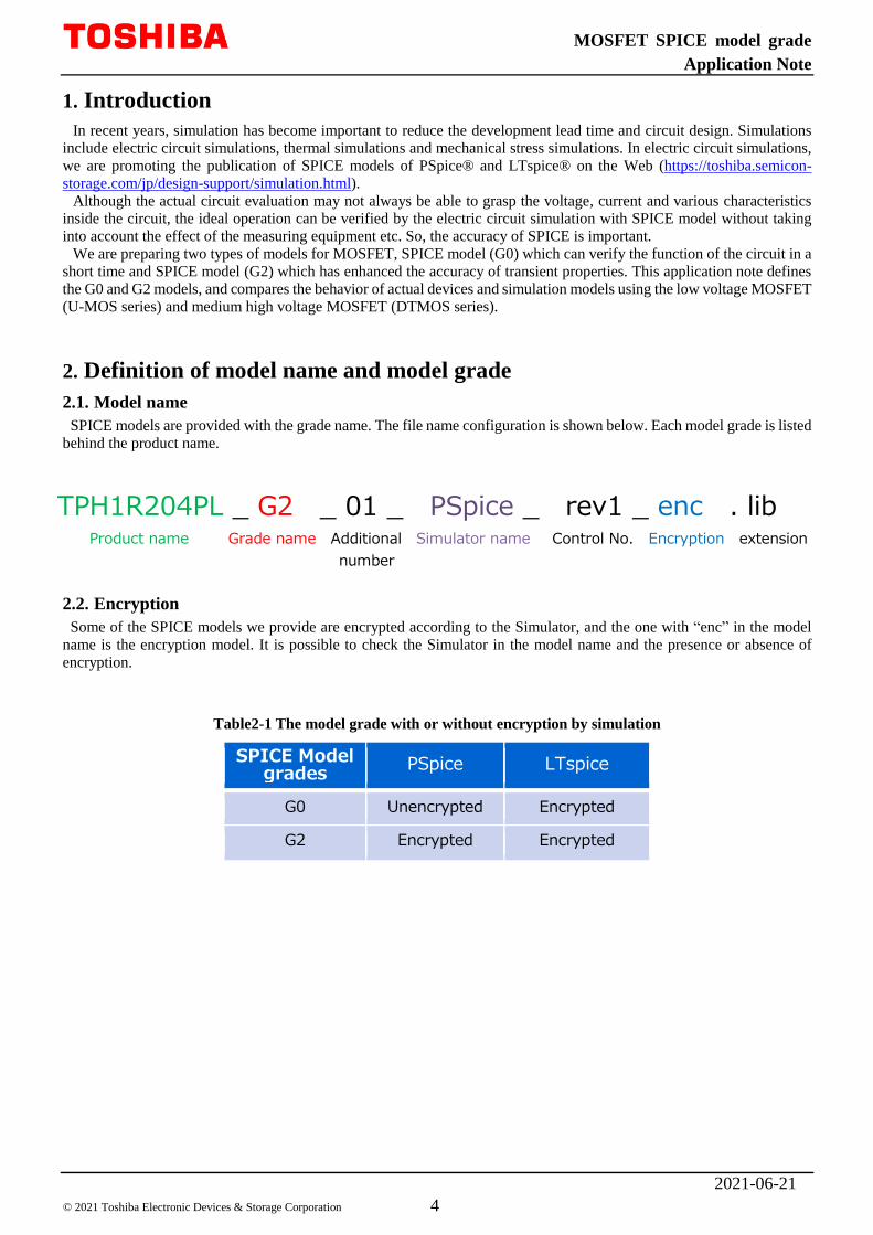
2. Definition of model name and model grade
2.1. Model name
SPICE models are provided with the grade name. The file name configuration is shown below. Each model grade is listed
behind the product name.
2.2. Encryption
Some of the SPICE models we provide are encrypted according to the Simulator, and the one with “enc” in the model
name is the encryption model. It is possible to check the Simulator in the model name and the presence or absence of
encryption.
Table2-1 The model grade with or without encryption by simulation
SPICE Model grades
PSpice LTspice
G0 Unencrypted Encrypted
G2 Encrypted Encrypted
TPH1R204PL _ G2 _ 01 _ PSpice _ rev1 _ enc . lib Product name Grade name Additional Simulator name Control No. Encryption extension
number

MOSFET SPICE model grade
Application Note
2021-06-21
5 © 2021 Toshiba Electronic Devices & Storage Corporation
2.3. Definition of model grades G0 and G2
Table 2-2 shows the reproducibility of the characteristic curve by the grade. The percentage in the table indicate the
RMS error (Root Mean Square) that is currently used as the criteria for modeling. The higher the grade, the higher the
fitting accuracy to the characteristic curve, which allows more accurate simulations. On the other hand, we recommend
that you select the suitable model grade for your simulation environment and purpose because there is a trade-off
relationship between fitting accuracy and convergence and time of calculations.
Table 2-2 Model Grade and Characteristic Curve Reproducibility
① G0
It is a standard device model based on BSIM3 and is a model with short calculation speed and suitable for function
checking.
② G2
Compared with the G0 model, this model enhances the reproducibility of the high current region characteristics of ID-
VDS curve and the voltage dependent characteristics of the parasitic capacitance, enabling highly accurate switching
simulations that are closer to actual measurements.
SPICE Model grades
ID-VDS Crss-VDS Coss-VDS Ciss-VDS
G0 (RMS error criterion)
○ (10% or less)
× (Not applicable)
× (Not applicable)
× (Not applicable)
G2 (RMS error criterion)
○ (5% or less)
○ (2% or less)
○ (2% or less)
○ (2% or less)

MOSFET SPICE model grade
Application Note
2021-06-21
6 © 2021 Toshiba Electronic Devices & Storage Corporation
3. Fitting accuracy (RMS error)
The fitting accuracy of SPICE model can be quantified by RMS error. For MOSFETs, this RMS error is used when
determining the accuracy of the created SPICE model, and the difference from the actual measurement is quantified and
we use them as the criteria. Figure 3-1 shows the RMS-error formulas used in creating the MOSFET SPICE models we
provide.
Chapters 4 and 5 show examples of low voltage MOSFET (U-MOS series) and medium high voltage MOSFET
(DTMOS series).
Figure 3-1 RMS error expression used when creating a Web published device model

MOSFET SPICE model grade
Application Note
2021-06-21
7 © 2021 Toshiba Electronic Devices & Storage Corporation
Fitting accuracy comparison of G0 and G2 model in U-MOS series
4.1 ID-VDS curve (TPH5R60APL)
U-MOS Series is a MOSFET Series with a trench gate structure with 12V~300V withstand voltage. Fig. 4-1 shows a
fitting curve sample for ID-VDS. The slope of ID from low VGS to high VGS can be simulated, and good fitting accuracy is
achieved with 2.43% RMS failure for both the G0 and G2 models.
G0 model (RMS error: 2.43%) G2 model (RMS error: 2.43%)
Figure 4-1 ID-VDS Characteristics curve simulated by G0 and G2 models and data sheet
MOSFET SPICE model grade
Application Note
2021-06-21
8 © 2021 Toshiba Electronic Devices & Storage Corporation
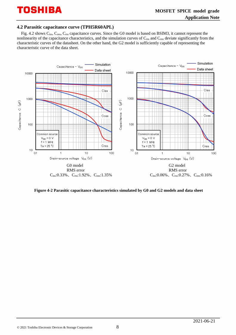
4.2 Parasitic capacitance curve (TPH5R60APL)
Fig. 4.2 shows Ciss, Coss, Crss capacitance curves. Since the G0 model is based on BSIM3, it cannot represent the
nonlinearity of the capacitance characteristics, and the simulation curves of Crss and Coss deviate significantly from the
characteristic curves of the datasheet. On the other hand, the G2 model is sufficiently capable of representing the
characteristic curve of the data sheet.
G0 model G2 model
RMS error RMS error
Ciss:0.33%、Crss:1.92%、Coss:1.35% Ciss:0.06%、Crss:0.27%、Coss:0.16%
Figure 4-2 Parasitic capacitance characteristics simulated by G0 and G2 models and data sheet
MOSFET SPICE model grade
Application Note
2021-06-21
9 © 2021 Toshiba Electronic Devices & Storage Corporation
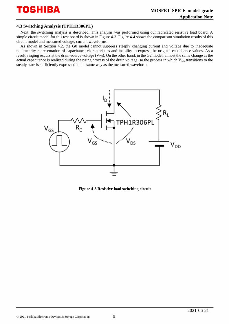
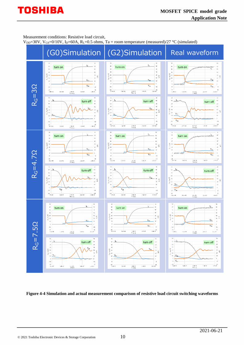
4.3 Switching Analysis (TPH1R306PL)
Next, the switching analysis is described. This analysis was performed using our fabricated resistive load board. A
simple circuit model for this test board is shown in Figure 4-3. Figure 4-4 shows the comparison simulation results of this
circuit model and measured voltage, current waveforms.
As shown in Section 4.2, the G0 model cannot suppress steeply changing current and voltage due to inadequate
nonlinearity representation of capacitance characteristics and inability to express the original capacitance values. As a
result, ringing occurs at the drain-source voltage (VDS). On the other hand, in the G2 model, almost the same change as the
actual capacitance is realized during the rising process of the drain voltage, so the process in which VDS transitions to the
steady state is sufficiently expressed in the same way as the measured waveform.
Figure 4-3 Resistive load switching circuit
MOSFET SPICE model grade
Application Note
2021-06-21
10 © 2021 Toshiba Electronic Devices & Storage Corporation
Figure 4-4 Simulation and actual measurement comparison of resistive load circuit switching waveforms
Measurement conditions: Resistive load circuit,
VDD=30V, VGS=0/10V, ID=60A, RL=0.5 ohms, Ta = room temperature (measured)/27 °C (simulated)
(G0)Simulation (G2)Simulation Real waveform
RG=3Ω
]]]]]]]
RG=4.7Ω
RG=7.5Ω
MOSFET SPICE model grade
Application Note
2021-06-21
11 © 2021 Toshiba Electronic Devices & Storage Corporation
5. Fitting accuracy comparison of G0 and G2 model in DTMOS series
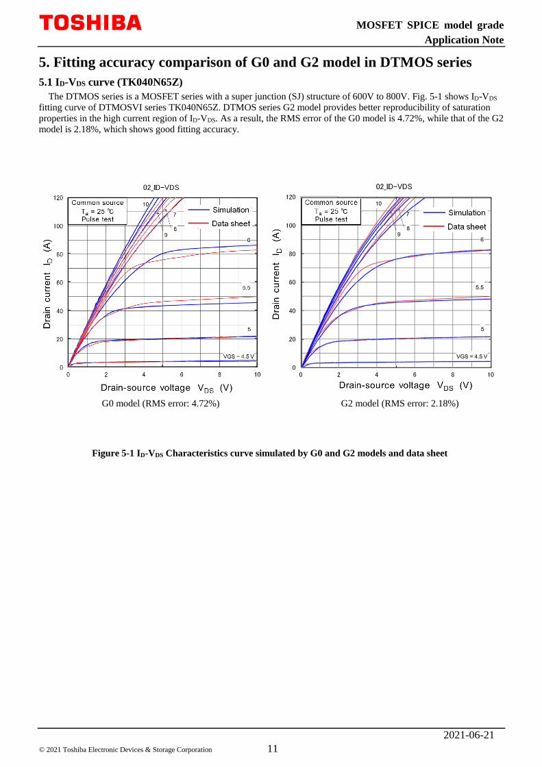
5.1 ID-VDS curve (TK040N65Z)
The DTMOS series is a MOSFET series with a super junction (SJ) structure of 600V to 800V. Fig. 5-1 shows ID-VDS
fitting curve of DTMOSVI series TK040N65Z. DTMOS series G2 model provides better reproducibility of saturation
properties in the high current region of ID-VDS. As a result, the RMS error of the G0 model is 4.72%, while that of the G2
model is 2.18%, which shows good fitting accuracy.
G0 model (RMS error: 4.72%) G2 model (RMS error: 2.18%)
Figure 5-1 ID-VDS Characteristics curve simulated by G0 and G2 models and data sheet

MOSFET SPICE model grade
Application Note
2021-06-21
12 © 2021 Toshiba Electronic Devices & Storage Corporation
5.2 Parasitic capacitance curve (TK040N65Z)
Fig. 5-2 shows Ciss, Coss, Crss capacitance curve. Since DTMOS series has a super-junction (SJ) structure, the Crss, Coss
curves for VDS decreases sharply from a certain voltage value. Since the G0 model is based on BSIM3, it is not possible
to express the non-linearity of this steeply decreasing capacitance characteristic, and the simulation curves of Crss and
Coss deviate significantly from the characteristic curve of the data sheet. On the other hand, the G2 model can express the
parasitic capacitance curve with an RMS error of 2% or less.
G0 model G2 model
RMS error RMS error
Ciss:0.53%、Crss:6.25%、Coss3.96% Ciss0.22%、Crss0.914%、Coss0.97%
Figure 5-2 Parasitic capacitance characteristics simulated by G0 and G2 models and data sheet
MOSFET SPICE model grade
Application Note
2021-06-21
13 © 2021 Toshiba Electronic Devices & Storage Corporation
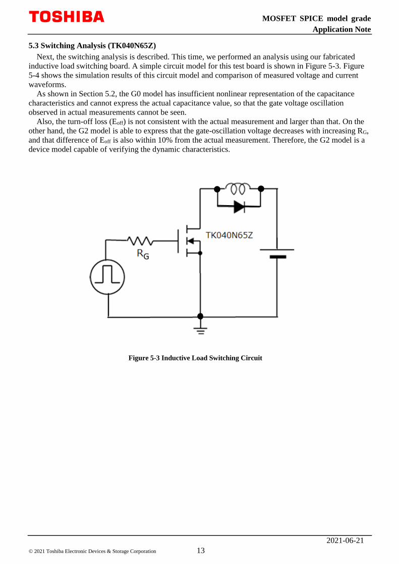
5.3 Switching Analysis (TK040N65Z)
Next, the switching analysis is described. This time, we performed an analysis using our fabricated
inductive load switching board. A simple circuit model for this test board is shown in Figure 5-3. Figure
5-4 shows the simulation results of this circuit model and comparison of measured voltage and current
waveforms.
As shown in Section 5.2, the G0 model has insufficient nonlinear representation of the capacitance
characteristics and cannot express the actual capacitance value, so that the gate voltage oscillation
observed in actual measurements cannot be seen.
Also, the turn-off loss (Eoff) is not consistent with the actual measurement and larger than that. On the
other hand, the G2 model is able to express that the gate-oscillation voltage decreases with increasing RG,
and that difference of Eoff is also within 10% from the actual measurement. Therefore, the G2 model is a
device model capable of verifying the dynamic characteristics.
Figure 5-3 Inductive Load Switching Circuit

MOSFET SPICE model grade
Application Note
2021-06-21
14 © 2021 Toshiba Electronic Devices & Storage Corporation
Measurement conditions: inductance load circuit,
VDD=400V, VGS=0/10V, ID=10A, Ta = room temperature (measured)/27°C (simulated)
(G0)Simulation (G2)Simulation Real waveform
RG=
10Ω
Eoff=100μJ
Eoff=18μJ
Eoff=20μJ
RG=
27Ω
Eoff=184μJ
Eoff=31μJ
Eoff=35μJ
RG=
47Ω
Eoff=450μJ
Eoff=81μJ
Eoff=80μJ
-10
-5
0
5
10
15
VGS(V)
0
5
10
15
20
25
0
100
200
300
400
500
3.0E-06 3.2E-06 3.4E-06 3.6E-06 3.8E-06 4.0E-06
ID (A)
VDS(V)
Time(s)
-10
-5
0
5
10
15
VGS(V)
0
5
10
15
20
25
0
100
200
300
400
500
3.0E-06 3.2E-06 3.4E-06 3.6E-06 3.8E-06 4.0E-06
ID (A)
VDS(V)
Time(s)
-10
-5
0
5
10
15
VGS(V)
0
5
10
15
20
25
0
100
200
300
400
500
-1.5E-07 5.0E-08 2.5E-07 4.5E-07 6.5E-07 8.5E-07
ID (A)
VDS(V)
Time(s)
-10
-5
0
5
10
15
VGS(V)
0
5
10
15
20
25
0
100
200
300
400
500
3.0E-06 3.2E-06 3.4E-06 3.6E-06 3.8E-06 4.0E-06
ID (A)
VDS(V)
Time(s)
-10
-5
0
5
10
15
VGS(V)
0
5
10
15
20
25
0
100
200
300
400
500
3.0E-06 3.2E-06 3.4E-06 3.6E-06 3.8E-06 4.0E-06
ID (A)
VDS(V)
Time(s)
-10
-5
0
5
10
15
VGS(V)
0
5
10
15
20
25
0
100
200
300
400
500
-1.5E-07 5.0E-08 2.5E-07 4.5E-07 6.5E-07 8.5E-07
ID (A)V
DS(V)
Time(s)
-10
-5
0
5
10
15
VGS(V)
0
5
10
15
20
25
0
100
200
300
400
500
3.0E-06 3.2E-06 3.4E-06 3.6E-06 3.8E-06 4.0E-06
ID (A)
VDS(V)
Time(s)
-10
-5
0
5
10
15
VGS(V)
0
5
10
15
20
25
0
100
200
300
400
500
3.0E-06 3.2E-06 3.4E-06 3.6E-06 3.8E-06 4.0E-06
ID (A)
VDS(V)
Time(s)
-10
-5
0
5
10
15
VGS(V)
0
5
10
15
20
25
0
100
200
300
400
500
-1.5E-07 5.0E-08 2.5E-07 4.5E-07 6.5E-07 8.5E-07
ID (A)V
DS(V)
Time(s)
Figure 5-4 Simulation and actual measurement comparison of inductive load circuit switching waveforms
MOSFET SPICE model grade
Application Note
2021-06-21
15 © 2021 Toshiba Electronic Devices & Storage Corporation
RESTRICTIONS ON PRODUCT USE
Toshiba Corporation and its subsidiaries and affiliates are collectively referred to as “TOSHIBA”. Hardware, software and systems described in this document are collectively referred to as “Product”.
• TOSHIBA reserves the right to make changes to the information in this document and related Product without notice.
• This document and any information herein may not be reproduced without prior written permission from TOSHIBA. Even with TOSHIBA's
written permission, reproduction is permissible only if reproduction is without alteration/omission.
• Though TOSHIBA works continually to improve Product's quality and reliability, Product can malfunction or fail. Customers are responsible for
complying with safety standards and for providing adequate designs and safeguards for their hardware, software and systems which minimize risk and avoid situations in which a malfunction or failure of Product could cause loss of human life, bodily injury or damage to property, including data loss or corruption. Before customers use the Product, create designs including the Product, or incorporate the Product into their own applications, customers must also refer to and comply with (a) the latest versions of all relevant TOSHIBA information, including without limitation, this document, the specifications, the data sheets and application notes for Product and the precautions and conditions set forth in the "TOSHIBA Semiconductor Reliability Handbook" and (b) the instructions for the application with which the Product will be used with or for. Customers are solely responsible for all aspects of their own product design or applications, including but not limited to (a) determining the appropriateness of the use of this Product in such design or applications; (b) evaluating and determining the applicability of any information contained in this document, or in charts, diagrams, programs, algorithms, sample application circuits, or any other referenced documents; and (c) validating all operating parameters for such designs and applications. TOSHIBA ASSUMES NO LIABILITY FOR CUSTOMERS' PRODUCT DESIGN OR APPLICATIONS.
• PRODUCT IS NEITHER INTENDED NOR WARRANTED FOR USE IN EQUIPMENTS OR SYSTEMS THAT REQUIRE
EXTRAORDINARILY HIGH LEVELS OF QUALITY AND/OR RELIABILITY, AND/OR A MALFUNCTION OR FAILURE OF WHICH MAY CAUSE LOSS OF HUMAN LIFE, BODILY INJURY, SERIOUS PROPERTY DAMAGE AND/OR SERIOUS PUBLIC IMPACT ("UNINTENDED USE"). Except for specific applications as expressly stated in this document, Unintended Use includes, without limitation, equipment used in nuclear facilities, equipment used in the aerospace industry, lifesaving and/or life supporting medical equipment, equipment used for automobiles, trains, ships and other transportation, traffic signaling equipment, equipment used to control combustions or explosions, safety devices, elevators and escalators, and devices related to power plant. IF YOU USE PRODUCT FOR UNINTENDED USE, TOSHIBA ASSUMES NO LIABILITY FOR PRODUCT. For details, please contact your TOSHIBA sales representative or contact us via our website.
• Do not disassemble, analyze, reverse-engineer, alter, modify, translate or copy Product, whether in whole or in part.
• Product shall not be used for or incorporated into any products or systems whose manufacture, use, or sale is prohibited under any applicable
laws or regulations.
• The information contained herein is presented only as guidance for Product use. No responsibility is assumed by TOSHIBA for any
infringement of patents or any other intellectual property rights of third parties that may result from the use of Product. No license to any intellectual property right is granted by this document, whether express or implied, by estoppel or otherwise.
• ABSENT A WRITTEN SIGNED AGREEMENT, EXCEPT AS PROVIDED IN THE RELEVANT TERMS AND CONDITIONS OF SALE FOR
PRODUCT, AND TO THE MAXIMUM EXTENT ALLOWABLE BY LAW, TOSHIBA (1) ASSUMES NO LIABILITY WHATSOEVER, INCLUDING WITHOUT LIMITATION, INDIRECT, CONSEQUENTIAL, SPECIAL, OR INCIDENTAL DAMAGES OR LOSS, INCLUDING WITHOUT LIMITATION, LOSS OF PROFITS, LOSS OF OPPORTUNITIES, BUSINESS INTERRUPTION AND LOSS OF DATA, AND (2) DISCLAIMS ANY AND ALL EXPRESS OR IMPLIED WARRANTIES AND CONDITIONS RELATED TO SALE, USE OF PRODUCT, OR INFORMATION, INCLUDING WARRANTIES OR CONDITIONS OF MERCHANTABILITY, FITNESS FOR A PARTICULAR PURPOSE, ACCURACY OF INFORMATION, OR NONINFRINGEMENT.
• Do not use or otherwise make available Product or related software or technology for any military purposes, including without limitation, for
the design, development, use, stockpiling or manufacturing of nuclear, chemical, or biological weapons or missile technology products (mass destruction weapons). Product and related software and technology may be controlled under the applicable export laws and regulations including, without limitation, the Japanese Foreign Exchange and Foreign Trade Law and the U.S. Export Administration Regulations. Export and re-export of Product or related software or technology are strictly prohibited except in compliance with all applicable export laws and regulations.
• Please contact your TOSHIBA sales representative for details as to environmental matters such as the RoHS compatibility of Product. Please
use Product in compliance with all applicable laws and regulations that regulate the inclusion or use of controlled substances, including without limitation, the EU RoHS Directive. TOSHIBA ASSUMES NO LIABILITY FOR DAMAGES OR LOSSES OCCURRING AS A RESULT OF NONCOMPLIANCE WITH APPLICABLE LAWS AND REGULATIONS.
Toshiba Electronic Device & Strage Corporation
https://toshiba.semicon-storage.com/jp/
Fig. 3-0-RMS error expression
https://toshiba.semicon-
storage.com/jp/(Link) used when creating 5
Web public device model01
Fig. 3-0-RMS error expression
https://toshiba.semicon-
storage.com/jp/(Link) used when creating 6
Web public device model02
Fig. 3-0-RMS error expression
https://toshiba.semicon-
storage.com/jp/(Link) used when creating 7
Web public device model03