Embed Size (px)
Citation preview
CMOS Digital Integrated Circuits1
CMOS Digital Integrated Circuits
Lec 5
SPICE Modeling of MOSFET
CMOS Digital Integrated Circuits2
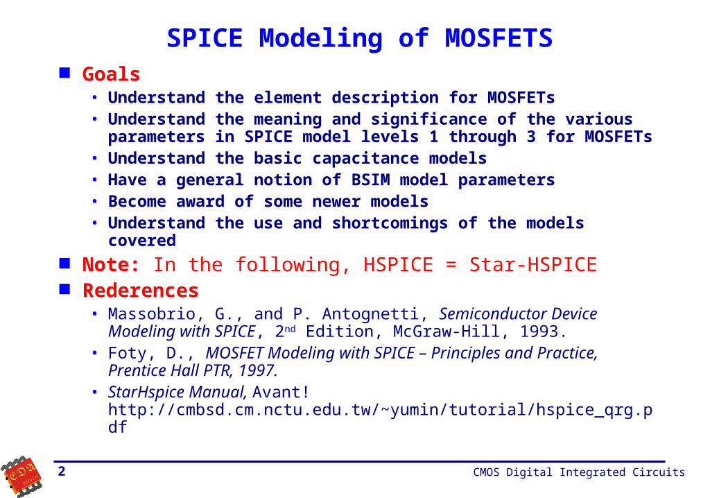
SPICE Modeling of MOSFETS Goals
• Understand the element description for MOSFETs• Understand the meaning and significance of the various parameters
in SPICE model levels 1 through 3 for MOSFETs• Understand the basic capacitance models• Have a general notion of BSIM model parameters• Become award of some newer models• Understand the use and shortcomings of the models covered
Note: In the following, HSPICE = Star-HSPICE Rederences
• Massobrio, G., and P. Antognetti, Semiconductor Device Modeling with SPICE, 2nd Edition, McGraw-Hill, 1993.
• Foty, D., MOSFET Modeling with SPICE – Principles and Practice, Prentice Hall PTR, 1997.
• StarHspice Manual, Avant! http://cmbsd.cm.nctu.edu.tw/~yumin/tutorial/hspice_qrg.pdf
CMOS Digital Integrated Circuits3
The MOSFET Description LinesModel and Element
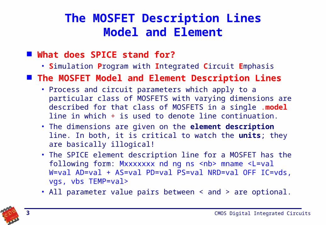
What does SPICE stand for?• Simulation Program with Integrated Circuit Emphasis
The MOSFET Model and Element Description Lines• Process and circuit parameters which apply to a particular class of
MOSFETS with varying dimensions are described for that class of MOSFETS in a single .model line in which + is used to denote line continuation.
• The dimensions are given on the element description line. In both, it is critical to watch the units; they are basically illogical!
• The SPICE element description line for a MOSFET has the following form: Mxxxxxxx nd ng ns <nb> mname <L=val W=val AD=val + AS=val PD=val PS=val NRD=val OFF IC=vds, vgs, vbs TEMP=val>
• All parameter value pairs between < and > are optional.
CMOS Digital Integrated Circuits4
The MOSFET Description LinesElement Line (Continued)
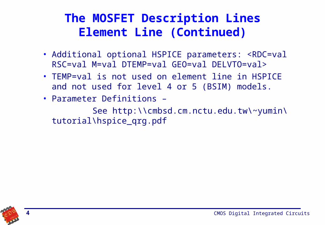
• Additional optional HSPICE parameters: <RDC=val RSC=val M=val DTEMP=val GEO=val DELVTO=val>
• TEMP=val is not used on element line in HSPICE and not used for level 4 or 5 (BSIM) models.
• Parameter Definitions –
See http:\\cmbsd.cm.nctu.edu.tw\~yumin\tutorial\hspice_qrg.pdf
CMOS Digital Integrated Circuits5
DC SPICE ModelsLevel 1 (Shichman-Hodges) DC Model
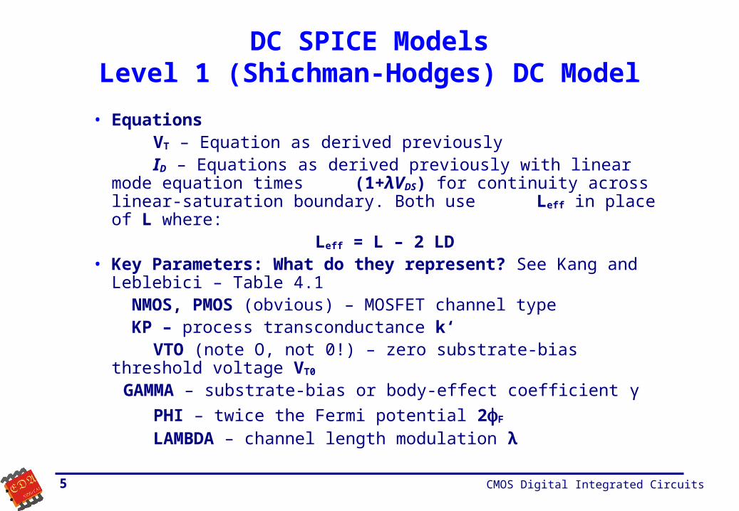
• Equations VT – Equation as derived previously ID – Equations as derived previously with linear mode equation times
(1+λVDS) for continuity across linear-saturation boundary. Both use Leff in place of L where:
Leff = L – 2 LD• Key Parameters: What do they represent? See Kang and Leblebici –
Table 4.1 NMOS, PMOS (obvious) – MOSFET channel type KP – process transconductance k‘
VTO (note O, not 0!) – zero substrate-bias threshold voltage VT0
GAMMA – substrate-bias or body-effect coefficient γ
PHI – twice the Fermi potential 2F
LAMBDA – channel length modulation λ
CMOS Digital Integrated Circuits6
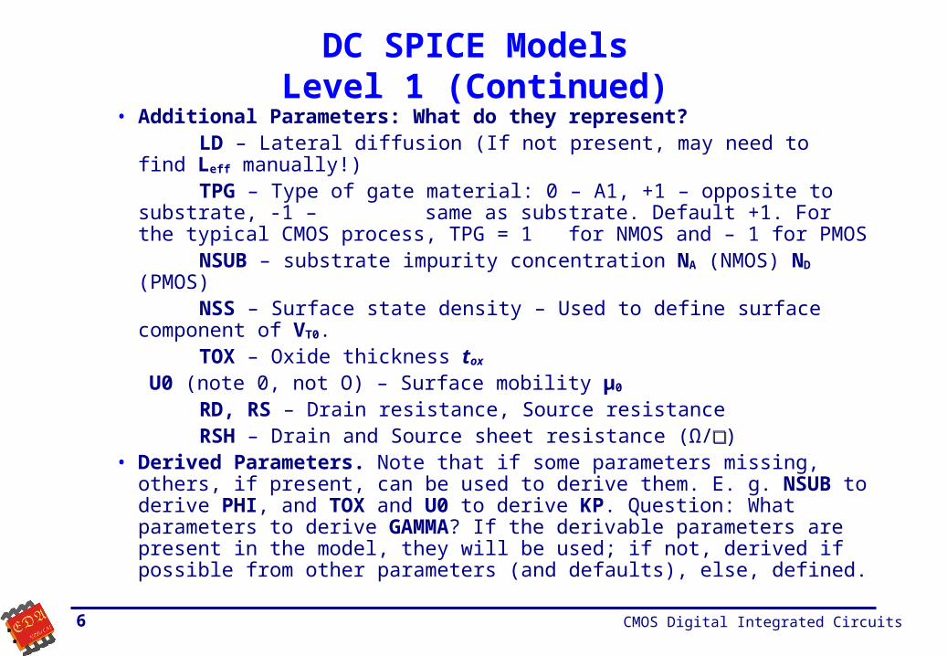
DC SPICE ModelsLevel 1 (Continued)
• Additional Parameters: What do they represent? LD – Lateral diffusion (If not present, may need to find Leff manually!) TPG – Type of gate material: 0 – A1, +1 – opposite to substrate, -1 –
same as substrate. Default +1. For the typical CMOS process, TPG = 1 for NMOS and – 1 for PMOS
NSUB – substrate impurity concentration NA (NMOS) ND (PMOS) NSS – Surface state density – Used to define surface component of VT0. TOX – Oxide thickness tox
U0 (note 0, not O) – Surface mobility µ0
RD, RS – Drain resistance, Source resistance RSH – Drain and Source sheet resistance (Ω/□□) • Derived Parameters. Note that if some parameters missing, others, if
present, can be used to derive them. E. g. NSUB to derive PHI, and TOX and U0 to derive KP. Question: What parameters to derive GAMMA? If the derivable parameters are present in the model, they will be used; if not, derived if possible from other parameters (and defaults), else, defined.
CMOS Digital Integrated Circuits7
DC SPICE ModelsLevel 2
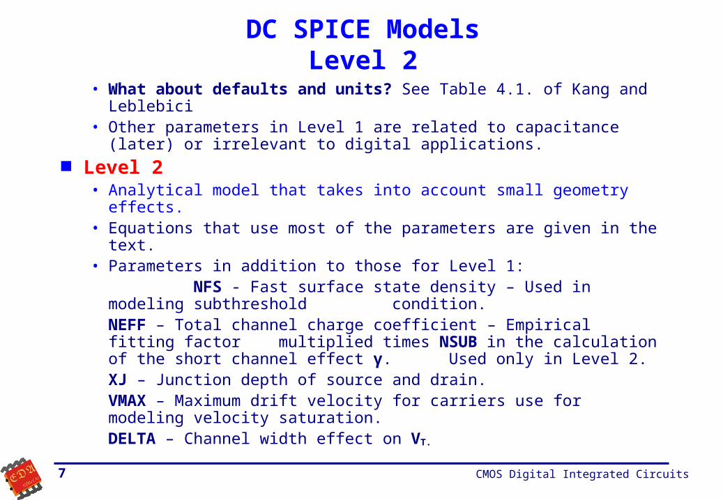
• What about defaults and units? See Table 4.1. of Kang and Leblebici• Other parameters in Level 1 are related to capacitance (later) or
irrelevant to digital applications. Level 2
• Analytical model that takes into account small geometry effects.• Equations that use most of the parameters are given in the text.• Parameters in addition to those for Level 1: NFS - Fast surface state density – Used in modeling subthreshold
condition. NEFF – Total channel charge coefficient – Empirical fitting
factor multiplied times NSUB in the calculation of the short channel effect γ. Used only in Level 2.
XJ – Junction depth of source and drain.VMAX – Maximum drift velocity for carriers use for modeling
velocity saturation.DELTA – Channel width effect on VT.
CMOS Digital Integrated Circuits8
DC SPICE ModelsLevel 2 (Continued)
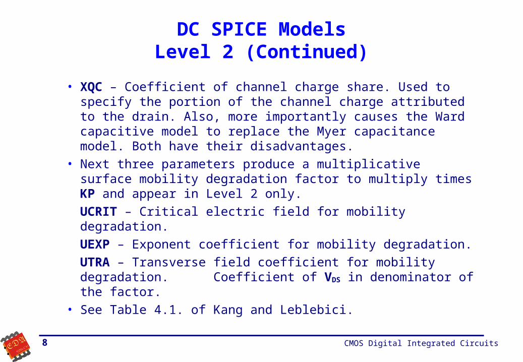
• XQC – Coefficient of channel charge share. Used to specify the portion of the channel charge attributed to the drain. Also, more importantly causes the Ward capacitive model to replace the Myer capacitance model. Both have their disadvantages.
• Next three parameters produce a multiplicative surface mobility degradation factor to multiply times KP and appear in Level 2 only.
UCRIT – Critical electric field for mobility degradation.
UEXP – Exponent coefficient for mobility degradation.
UTRA – Transverse field coefficient for mobility degradation. Coefficient of VDS in denominator of the factor.
• See Table 4.1. of Kang and Leblebici.
CMOS Digital Integrated Circuits9
DC SPICE ModelsLevel 3
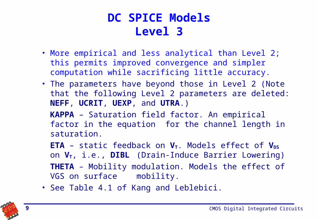
• More empirical and less analytical than Level 2; this permits improved convergence and simpler computation while sacrificing little accuracy.
• The parameters have beyond those in Level 2 (Note that the following Level 2 parameters are deleted: NEFF, UCRIT, UEXP, and UTRA.)
KAPPA – Saturation field factor. An empirical factor in the equation for the channel length in saturation.
ETA – static feedback on VT. Models effect of VDS on VT, i.e., DIBL (Drain-Induce Barrier Lowering)
THETA – Mobility modulation. Models the effect of VGS on surface mobility.
• See Table 4.1 of Kang and Leblebici.
CMOS Digital Integrated Circuits10
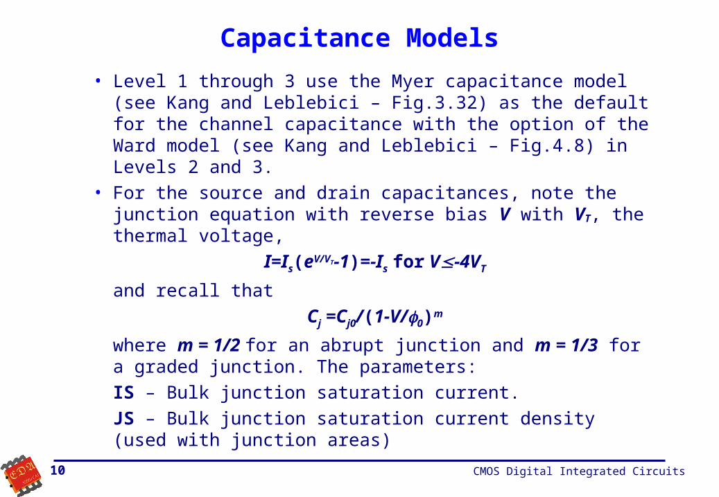
Capacitance Models
• Level 1 through 3 use the Myer capacitance model (see Kang and Leblebici – Fig.3.32) as the default for the channel capacitance with the option of the Ward model (see Kang and Leblebici – Fig.4.8) in Levels 2 and 3.
• For the source and drain capacitances, note the junction equation with reverse bias V with VT, the thermal voltage,
I=Is(eV/VT-1)=-Is for V-4VT
and recall that
Cj =Cj0/(1-V/0)m
where m = 1/2 for an abrupt junction and m = 1/3 for a graded junction. The parameters:
IS – Bulk junction saturation current.
JS – Bulk junction saturation current density (used with junction areas)
CMOS Digital Integrated Circuits11
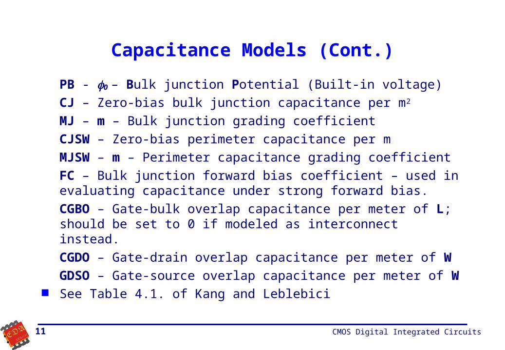
Capacitance Models (Cont.)
PB - 0 – Bulk junction Potential (Built-in voltage)
CJ – Zero-bias bulk junction capacitance per m2
MJ – m – Bulk junction grading coefficient
CJSW – Zero-bias perimeter capacitance per m
MJSW – m – Perimeter capacitance grading coefficient
FC – Bulk junction forward bias coefficient – used in evaluating capacitance under strong forward bias.
CGBO – Gate-bulk overlap capacitance per meter of L; should be set to 0 if modeled as interconnect instead.
CGDO – Gate-drain overlap capacitance per meter of W
GDSO – Gate-source overlap capacitance per meter of W See Table 4.1. of Kang and Leblebici
CMOS Digital Integrated Circuits12
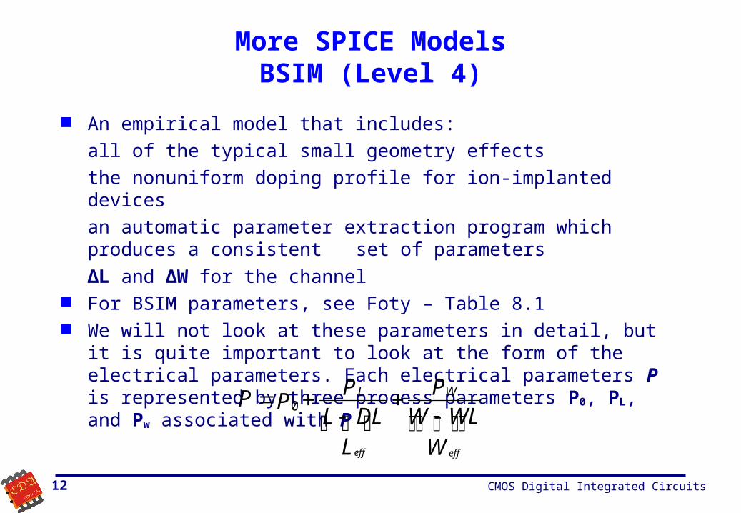
More SPICE ModelsBSIM (Level 4)
An empirical model that includes:
all of the typical small geometry effects
the nonuniform doping profile for ion-implanted devices
an automatic parameter extraction program which produces a consistent set of parameters
ΔL and ΔW for the channel For BSIM parameters, see Foty – Table 8.1 We will not look at these parameters in detail, but it is quite important to
look at the form of the electrical parameters. Each electrical parameters P is represented by three process parameters P0, PL, and Pw associated with P
W
WLWP
LDLL
PPP
effeff
WL
0
CMOS Digital Integrated Circuits13
SPICE ModelsBSIM (Cont.)
L and W are drawn dimensions and DL and DW are the net size changes in the drawn dimensions due to the entire sequence of fabrication steps. The difference shown give Leff and Weff. The equation for P allows for an adjustment of the electrical parameter as a function of the effective length and width of the channel
Parameter extraction uses devices sizes. P0 is for long, wide MOSFET. BSIM also uses a new approach to capacitance modeling that avoids the
difficulties of errors and lack of charge conservation in the Meyer model and the errors and convergence problems in the Ward model.
See Massobrio and Antognetti – p. 219 for trios of parameters. Note that model file has only numerical values identified by position; this is
an alternate form of the model that cryptic.
CMOS Digital Integrated Circuits14
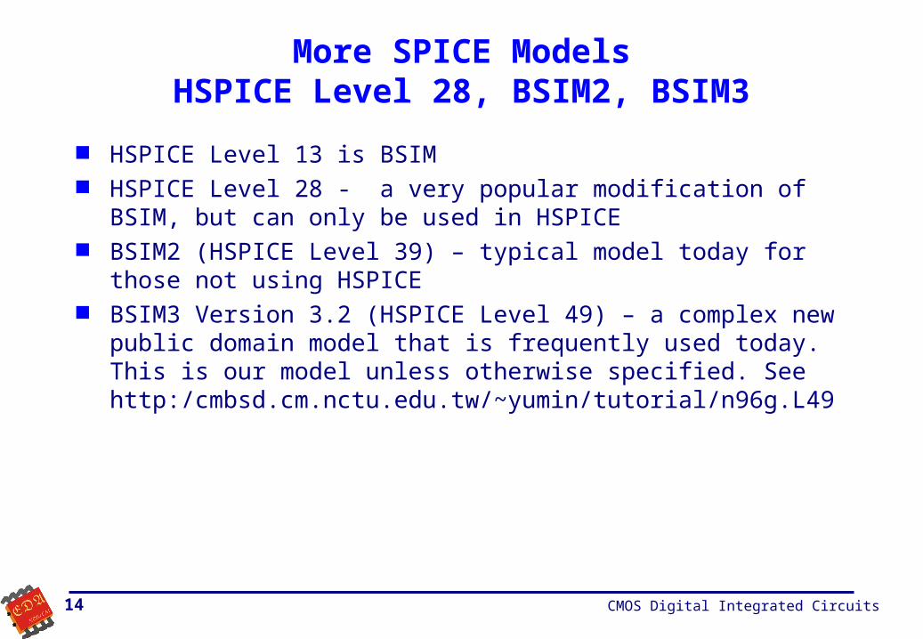
More SPICE ModelsHSPICE Level 28, BSIM2, BSIM3
HSPICE Level 13 is BSIM HSPICE Level 28 - a very popular modification of BSIM, but can only be
used in HSPICE BSIM2 (HSPICE Level 39) – typical model today for those not using
HSPICE BSIM3 Version 3.2 (HSPICE Level 49) – a complex new public domain
model that is frequently used today. This is our model unless otherwise specified. See http:/cmbsd.cm.nctu.edu.tw/~yumin/tutorial/n96g.L49
CMOS Digital Integrated Circuits15
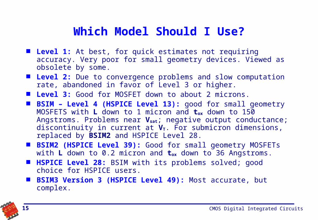
Which Model Should I Use?
Level 1: At best, for quick estimates not requiring accuracy. Very poor for small geometry devices. Viewed as obsolete by some.
Level 2: Due to convergence problems and slow computation rate, abandoned in favor of Level 3 or higher.
Level 3: Good for MOSFET down to about 2 microns. BSIM – Level 4 (HSPICE Level 13): good for small geometry MOSFETS
with L down to 1 micron and tox down to 150 Angstroms. Problems near Vsat; negative output conductance; discontinuity in current at VT. For submicron dimensions, replaced by BSIM2 and HSPICE Level 28.
BSIM2 (HSPICE Level 39): Good for small geometry MOSFETs with L down to 0.2 micron and tox down to 36 Angstroms.
HSPICE Level 28: BSIM with its problems solved; good choice for HSPICE users.
BSIM3 Version 3 (HSPICE Level 49): Most accurate, but complex.
CMOS Digital Integrated Circuits16
Summary
Learned the element description line for MOSFET Reviewed the first generation SPICE model parameters, levels 1, 2, and 3 Reviewed the device capacitances and associated parameters for the BSIM
model Obtained a sense of the form of the parameters for the BSIM model Obtained an awareness of some of the newer models Obtained a comparative viewpoint of the models and their use.