Embed Size (px)
Citation preview

MOSFET and Front-End ProcessIntegration: Scalin g, Challen ges, and
Potential Solutions Throu gh the End ofthe Roadmap
Tutorial, Hot Chips ConferenceStanford UniversitySunday, August 18, 2002Morning Session
Peter M. Zeitzoff,International SEMATECH, Austin, TX

P. Zeitzoff, MOSFET and Front-end Scaling: Hot Chips Tutorial, 8/18/02 -- p.2
Outline
• Introduction/ITRS
• MOSFET scaling and its impact
• Front-end approaches and solutions
• Non-classical CMOS
• Conclusions

P. Zeitzoff, MOSFET and Front-end Scaling: Hot Chips Tutorial, 8/18/02 -- p.3
Introduction• IC technology: following Moore’s Law by rapidly scaling
into deep submicron regime (currently, 130nm technologygeneration)
– Increased speed– Lower power dissipation per function– Increased transistor and function density– Lower cost/function
• The scaling results in major MOSFET and processintegration issues, including
– Simultaneously maintaining satisfactory Ion (drive current) and Ileak
– High gate leakage current for very thin gate dielectrics– Fabrication and control of very abrupt, shallow, low sheet resistance
S/D extensions– Control of short channel effects for very small transistors– Etc.
• Potential solutions & approaches:– Material and process (front end): high K gate dielectric, metal gate
electrodes,…– Structural: non-classical CMOS device structures

P. Zeitzoff, MOSFET and Front-end Scaling: Hot Chips Tutorial, 8/18/02 -- p.4
International Technolo gy Roadmap forSemiconductors (ITRS)• Industry-wide, fully international effort to map IC
technology generations for the next 15 years– For each technology generation
• Projects targets for technology characteristics and requirements
• Assesses key needs and gaps
• Lists potential solutions
– Provides common reference for semiconductor industry: devicemanufacturers, equipment and materials vendors, researchers
• Is not meant to restrict research, pick winners– Focus: stimulating needed R&D
• Useful for planning
– Enabling factor in continuing to follow Moore’s Law
– Most of projections in this talk from 2001 ITRS

P. Zeitzoff, MOSFET and Front-end Scaling: Hot Chips Tutorial, 8/18/02 -- p.5
Key Overall Chip Parameters for Hi gh-Performance Lo gic, from 2001 ITRS
2001 2002 2003 2004 2005 2006 2007 2010 2013 2016
DRAM Half PItch nm 130 115 100 90 80 70 65 45 35 22
Physical Gate Length, L g nm 65 53 45 37 32 28 25 18 13 9
Nominal Power Supply Voltage (Vdd) V 1.2 1.1 1.0 1.0 0.9 0.9 0.7 0.6 0.5 0.4
Maximum on-chip local clock frequency GHz 1.7 2.3 3.1 4.0 5.2 5.6 6.7 11.5 19.4 28.8
Allowable maximum power dissipation, with heatsink
W 130 140 150 160 170 180 190 218 215 288
Number of transistors per chipMillions of transistors
276 348 439 553 697 878 1106 2212 4424
Calendar Year
8848
Near Term Long Term
•The DRAM half pitch and L g are drivers of IC technology scaling, including lithography(to be discussed by Prof. Wong)
•Technology generations (in red) defined by DRAM half pitch
•This is a dense feature: drives functional density
–Reduction factor of 0.7X ~ 1/ • 2 between generations (130nm in 2001, 90nm in 2004,65nm in 2007, etc.)h
–Three years between generations
–Gate length (L g) ≤ 0.5 X DRAM half pitch
–These are isolated features
–Rapid scaling of L g is driven by need to improve transistor speed

P. Zeitzoff, MOSFET and Front-end Scaling: Hot Chips Tutorial, 8/18/02 -- p.6
2001 vs. 1999 ITRS Projections of Physical GateLength (L g): High Performance Lo gic
0
10
20
30
40
50
60
70
80
90
100
2000 2002 2004 2006 2008 2010 2012 2014 2016
Year
Lg (
nm)
Lg, ’01ITRS
Lg, ’99ITRS
P. Zeitzoff, MOSFET and Front-end Scaling: Hot Chips Tutorial, 8/18/02 -- p.7
Outline
• Introduction/ITRS
• MOSFET scaling and its impact
• Front-end approaches and solutions
• Non-classical CMOS
• Conclusions

P. Zeitzoff, MOSFET and Front-end Scaling: Hot Chips Tutorial, 8/18/02 -- p.8
Hierarch y of IC Requirements and Choices
Overall Circuit Requirements
and Choices
OverallMOSFET
Requirements and Choices
MOSFETDesign
Choices
ProcessIntegration
Choices
•Chip Power
•Chip Speed
•FunctionalDensity
•Chip Cost
•Architecture
•Etc.
•Vdd
•MOSFETLeakage
•MOSFET Drivecurrent
•Parasitic seriesresistance
•Transistor size
•Vt control
•Reliability
•Etc.
•Tox, Lg, xj, Rs
•Channelengineering
•Oxynitride orHigh K gatedielec.
•Classical PlanarBulk or Non-classical CMOSStructures
•Etc.
•Thermalprocessing
•Overallprocess flow
•Processmodules
•Materialproperties
•Boronpenetration
•Etc.

P. Zeitzoff, MOSFET and Front-end Scaling: Hot Chips Tutorial, 8/18/02 -- p.9
Historical Data and ITRS Projections for ChipClock Frequency, Hi gh-Performance Lo gic
1
10
100
1,000
10,000
100,000
1980 1985 1990 1995 2000 2005 2010 2015
Fre
quen
cy (
MH
z)
2X / 4 Years
2X / 2 - 2½ Years
2X / 2½ YearsMPU Clock FrequencyHistorical Trend:
Gate Scaling,TransistorDesigncontributed~ 17-19%/yearArchitectural Designinnovation contributedadditional~ 21-13%/year
Actual ScalingAcceleration , OrEquivalentScalingInnovationNeeded tomaintainhistorical trend
Historical <- > 1999 ITRS 2001 ITRS
Sources: Sematech, 2001 ITRS ORTC
Courtesy:Alan Allan,Intel

P. Zeitzoff, MOSFET and Front-end Scaling: Hot Chips Tutorial, 8/18/02 -- p.10
Impact of Key MOSFET Parameters on CircuitPerformance
Out
CL
In
Vdd
• Transistor intrinsic delay, τ– τ ~ C Vdd/(Ion*W)
• Ion units: µA/µm• C = Cs/d + CL
– Gate dominated (local, dense logic)• C ~ CL = Cgate ~ Cox*W*Lg + Cparasitic
• Cox ~ εox/Tox
– Interconnect dominated (long leads): C ~ CL ~ Cmetal
• We won’t consider this case: Mike Thomas will cover it inInterconnect lecture
• Transistor intrinsic switchin g frequency =1/ τ
– Good metric for transistor performance–To maximize 1/ τ, maximize I on

P. Zeitzoff, MOSFET and Front-end Scaling: Hot Chips Tutorial, 8/18/02 -- p.11
Frequency scalin g: Transistor Intrinsic(1/τ), Fanout-4 Gate, Chip Clock
1
10
100
1000
10000
2001 2006 2011 2016
Calendar Year
Fre
quen
cy (
GH
z)
Transistor IntrinsicFrequency
Fanout-4 GateFrequency
Chip ClockFrequency
Estimatesfrom 2001ITRS—interconn-ect delaynotincluded

P. Zeitzoff, MOSFET and Front-end Scaling: Hot Chips Tutorial, 8/18/02 -- p.12
ITRS Drivers for Different Applications• High performance chips (MPU, for example)
– Driver: maximize chip speedÆmaximizetransistor performance
• Goal of ITRS scaling: 1/τ increases at ~17% per year, historical rate–Must maximize Ion–Consequently, Ileak is relatively high
• Low power chips (mobile applications)– Driver: minimize chip powerÆminimize Ileak (to
conserve battery power)• Goal of ITRS scaling: specific, low level of
Ileak• Consequently, 1/τ is considerably less than
for high-performance logic

P. Zeitzoff, MOSFET and Front-end Scaling: Hot Chips Tutorial, 8/18/02 -- p.13
Device Scalin g Approach: 2001 ITRS
• Simple models capturin g essential MOSFETphysics Æembedded in a spreadsheet
– Initial choice of scaled MOSFET parameters ismade
– Using spreadsheet, MOSFET parameters areiteratively varied to meet ITRS targets
• High Performance: 17%/year increase in 1/τ
• Low Power: specific, low level of leakage current
P. Zeitzoff, MOSFET and Front-end Scaling: Hot Chips Tutorial, 8/18/02 -- p.14
• Preference: scale V dd down rapidly with tech.generations
– To keep dynamic power dissipation (~Vdd2) within
acceptable bounds– For reliability, control of short channel effects (SCE),
general device scaling
• 1/Isd,leak exp. dependent on V t
• Ion stron gly dependent on gate overdrive, (V dd-Vt)
• Difficult tradeoffs between I on and I sd,leak , Vdd andVt with scalin g
Vdd and V t Device Scalin g Issues

P. Zeitzoff, MOSFET and Front-end Scaling: Hot Chips Tutorial, 8/18/02 -- p.15
ITRS Projections of V dd and V t Scalin g
0.0
0 .2
0 .4
0 .6
0 .8
1 .0
1 .2
2001 2003 2005 2007 2009 2011 2013 2015
Y ear
Vdd
, Vt (
V)
Vdd-Low Power
Vdd-High Perf.
Vt-Low PowerVt-High Perf.

P. Zeitzoff, MOSFET and Front-end Scaling: Hot Chips Tutorial, 8/18/02 -- p.16
ITRS Projected Scalin g of 1/τ and I sd,leakfor Hi gh Performance and Low Power
1 0 0
1 0 0 0
1 0 0 0 0
2 0 0 1 2 0 0 3 2 0 0 5 2 0 0 7 2 0 0 9 2 0 1 1 2 0 1 3 2 0 1 5
Year
1/ (
GH
z)
1 .E -0 6
1 .E -0 5
1 .E -0 4
1 .E -0 3
1 .E -0 2
1 .E -0 1
1 .E +0 0
1 .E +0 1
Isd,leak
(µA/µm
)
Isd,leak , High Perf.
Isd,leak , Low Power Driver
1/τ, LowPower
1/τ , High Perf.Driver

P. Zeitzoff, MOSFET and Front-end Scaling: Hot Chips Tutorial, 8/18/02 -- p.17
Key MOSFET Scalin g Results• High-performance logic
– Average 17%/yr improvement in 1/ τ is attained
– Isd,leak is very high, particularly for 2007 andbeyond Î chip static power dissipation scalingis an issue
• Assumption: I gate ≤ Isd,leak Î uncomfortably large I gate
• Low-power logic– Very low I sd,leak target is met
• Igate ≤ Isd,leak Î Igate is very low: difficult to meet this
– 1/τ scales considerably slower than for high-performance
P. Zeitzoff, MOSFET and Front-end Scaling: Hot Chips Tutorial, 8/18/02 -- p.18
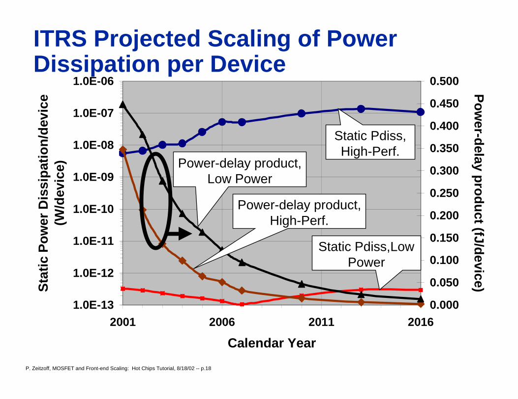
ITRS Projected Scalin g of PowerDissipation per Device
1.0E-13
1.0E-12
1.0E-11
1.0E-10
1.0E-09
1.0E-08
1.0E-07
1.0E-06
2001 2006 2011 2016
Calendar Year
Sta
tic P
ower
Dis
sipa
tion/
devi
ce
(W/d
evic
e)
0.000
0.050
0.100
0.150
0.200
0.250
0.300
0.350
0.400
0.450
0.500
Pow
er-delay product (fJ/device)
Static Pdiss,High-Perf.
Static Pdiss,LowPower
Power-delay product,Low Power
Power-delay product,High-Perf.
P. Zeitzoff, MOSFET and Front-end Scaling: Hot Chips Tutorial, 8/18/02 -- p.19
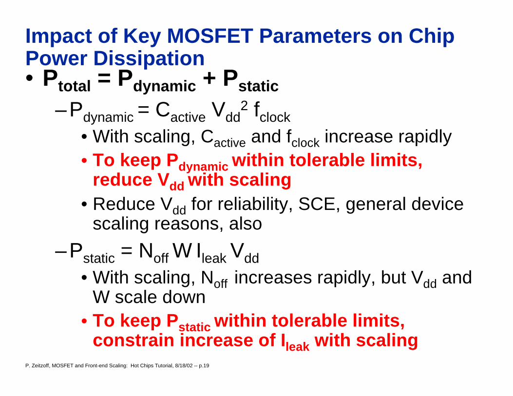
Impact of Key MOSFET Parameters on ChipPower Dissipation• Ptotal = Pdynamic + Pstatic
–Pdynamic = Cactive Vdd2 fclock
• With scaling, Cactive and fclock increase rapidly• To keep P dynamic within tolerable limits,
reduce V dd with scaling• Reduce Vdd for reliability, SCE, general device
scaling reasons, also
–Pstatic = Noff W Ileak Vdd
• With scaling, Noff increases rapidly, but Vdd andW scale down
• To keep P static within tolerable limits,constrain increase of I leak with scaling

P. Zeitzoff, MOSFET and Front-end Scaling: Hot Chips Tutorial, 8/18/02 -- p.20
Relative Chip Power Dissipation per ’01 ITRS,High Performance
1.E +00
1 .E +01
1 .E +02
1 .E +03
1 .E +04
20 01 20 03 20 05 20 07 20 09 20 11 20 13 20 15
Ye a r
Rel
ativ
e C
hip
Pow
er D
issi
patio
n N
orm
aliz
ed to
200
1
AllowableTotal ChipPowerDissipation
Chip Dynamic PowerDissipation
Chip Static PowerDissipation
Assumptions:
•Only one type of(high I on, high I leak)transistor, and nopower reductiontechniques.
•Simple scaling
•This is anunrealisticscenario, onlymeant to clearlyillustrate staticpower dissipationissues

P. Zeitzoff, MOSFET and Front-end Scaling: Hot Chips Tutorial, 8/18/02 -- p.21
Potential Solutions for Power DissipationProblems, Hi gh-Performance Lo gic
• Increasingly common approach: multipletransistor types on a chip Æmulti-Vt, multi-Tox, etc.
– Only utilize high-performance, high-leakage transistorsin critical paths—lower leakage transistors everywhereelse
– Improves flexibility for SOC
• Electrical or dynamically adjustable Vt devices(future possibility)
• Circuit and architectural techniques: pass gates,power down circuit blocks, etc .

P. Zeitzoff, MOSFET and Front-end Scaling: Hot Chips Tutorial, 8/18/02 -- p.22
Summary: MOSFET Scalin g• MOSFET scaling is the “raw material” for designers to
improve chip performance, control power dissipation– MOSFET scaling has historically contributed ~17% per year
in “raw” speed improvement for high-performance logic– Design and architectural innovation has contributed about
as much
• MOSFET scaling goals are critically important– High-performance logic emphasizes speed at the expense of
high leakage and static power dissipation– Low-power logic emphasizes low leakage at the expense of
speed– Dialogue between designers and technologists is essential
• Static power dissipation is a growing problem forhigh-performance logic, and there are numerousapproaches to dealing with it, esp. including design

P. Zeitzoff, MOSFET and Front-end Scaling: Hot Chips Tutorial, 8/18/02 -- p.23
Outline
• Introduction/ITRS
• MOSFET scaling and its impact
• Front-end approaches and solutions
• Non-classical CMOS
• Conclusions

P. Zeitzoff, MOSFET and Front-end Scaling: Hot Chips Tutorial, 8/18/02 -- p.24
Simplified Cross Section of a Typical PMOSFET andNMOSFET
(Not to scale)
Deep S/D: xj
Source/Drain
Deep Source/
Pre-Metal
p+ Poly Gate
PMOS Transistor
Shallow Trench Isolation (STI)
NMOS Transistor
n+ Poly Gate
P-Well
Salicided
and Poly
N-Well
Dielectric
Contact "Plug"
Drain (P+}
P -Epi
P+ Substitute
Gate OxideSource/DrainExtension (N)
Spacer
P+N+
Lg
Tox
S/D Extension: xj

P. Zeitzoff, MOSFET and Front-end Scaling: Hot Chips Tutorial, 8/18/02 -- p.25
Difficult Transistor Scalin g Issues• Previously discussed scaling results involve high-
level, idealized MOSFET physics– Assumption: highly scaled MOSFETs with required
characteristics can be successfully fabricated
• All lateral and vertical MOSFET dimensions (T ox,xj’s, spacer width, etc.) are scaling down rapidlyalong with L g
• With scaling, increasing difficulty in meetingtransistor requirements
– High gate leakage• Direct tunneling increases rapidly as T ox is reduced
– Poly depletion in gate electrode Æincreased effectiveTox, reduced I on
– Scaling S/D extension: x j – ρs-Æhigh R series,s/d , reducedIon
– Etc.

P. Zeitzoff, MOSFET and Front-end Scaling: Hot Chips Tutorial, 8/18/02 -- p.26
2001 ITRS Projections Versus Simulations of Direct Tunnelin gGate Leaka ge Current Density for Low Power Lo gic
1 .E -07
1 .E -06
1 .E -05
1 .E -04
1 .E -03
1 .E -02
1 .E -01
1 .E + 00
1 .E + 01
1 .E + 02
2001 2003 2005 2007 2009 2011 2013 2015
Ye a r
Jga
te (
A/c
m2 )
0
0 .5
1
1 .5
2
2 .5
3T
ox (nm)
Simulated J gate,oxynitride
SpecifiedJgate, ITRS
Tox
Beyond this point, oxynitridetoo leaky; high K needed
Implementation of hi gh K will be driven b y Low Power Lo gic in 2005
(Simulations courtesy of C. Osburn,NCSU and ITRS)

P. Zeitzoff, MOSFET and Front-end Scaling: Hot Chips Tutorial, 8/18/02 -- p.27
High K Gate Dielectric to Reduce Direct Tunnelin g
• Equivalent Oxide Thickness = EOT = T K * (3.9/K) = Tox, where 3.9 is relativedielectric constant of SiO2 and K is relative dielectric constant of high Kmaterial
– C = Cox = εox/Tox
– To first order, MOSFET characteristics with high-k are same as for SiO2
• Because T K > Tox, direct tunneling leakage much reduced with High K– If energy barrier is high enough
• Candidate materials: LaO 2/HfO2/ (K~15 - 30); Hf, Zr-SiO4 (K~12 - 16); others
Electrode
Si substrate
Tox SiO2
TK
High K Material
Electrode
Si substrate

P. Zeitzoff, MOSFET and Front-end Scaling: Hot Chips Tutorial, 8/18/02 -- p.28
High K Issues• Process integration issues
– Thermal stability of high K material• Conventional flow, with S/D anneal, etc., difficult
– “Replacement gate” flow is an option
– Thermal, chemical compatibility with polysilicon, & Bpenetration
• Metal electrode may be required
– Interface with Si substrate• Most form thin SiO2 layer: increases Tox,equiv
• Interface properties: increased surface states,fixed charge density; reduced mobility
• Leakage, reliability
• SCEÎfringe field effects
• New material: major challenge

P. Zeitzoff, MOSFET and Front-end Scaling: Hot Chips Tutorial, 8/18/02 -- p.29
Difficult Transistor Scalin g Issues• Previously discussed scaling results involve high-
level, idealized MOSFET physics– Assumption: highly scaled MOSFETs with required
characteristics can be successfully fabricated
• All lateral and vertical MOSFET dimensions (T ox,xj’s, spacer width, etc.) are scaling down rapidlyalong with L g
• With scaling, increasing difficulty in meetingtransistor requirements
– High gate leakage• Direct tunneling increases rapidly as T ox is reduced
– Poly depletion in gate electrode Æincreased effectiveTox, reduced I on
– Scaling S/D extension: x j – ρs-Æhigh R series,s/d , reducedIon
– Etc.

P. Zeitzoff, MOSFET and Front-end Scaling: Hot Chips Tutorial, 8/18/02 -- p.30
Polysilicon LimitationsPolysilicon depletion: band bendin g in the
polysilicon– Increases effective electrical ToxÎ reduces Eox, &
hence inversion charge– More of a problem as Tox is scaledÎ Poly doping
must increase with scaling• Ge-Si might help
• PMOSFETs: B penetration throu gh verythin oxides
– Oxy-nitrides & reduction of DT effective now
• Compatibility with hi gh K• Gate resistance of very thin gates (even
with silicide)

P. Zeitzoff, MOSFET and Front-end Scaling: Hot Chips Tutorial, 8/18/02 -- p.31
Metal Gate Electrodes• Metal gate electrodes are a potential
solution: probably implemented at 65nm tech. generation (2007) or beyond
–No depletion, very low resistance gate, noboron penetration, compatibility withhigh-k
– Issues• Different work functions needed for PMOS
and NMOS==>2 different metals needed– Process complexity, process integration
problems
• Etching of metal electrodes• New materials: major challenge

P. Zeitzoff, MOSFET and Front-end Scaling: Hot Chips Tutorial, 8/18/02 -- p.32
Difficult Transistor Scalin g Issues• Previously discussed scaling results involve high-
level, idealized MOSFET physics– Assumption: highly scaled MOSFETs with required
characteristics can be successfully fabricated
• All lateral and vertical MOSFET dimensions (T ox,xj’s, spacer width, etc.) are scaling down rapidlyalong with L g
• With scaling, increasing difficulty in meetingtransistor requirements
– High gate leakage• Direct tunneling increases rapidly as T ox is reduced
– Poly depletion in gate electrode Æincreased effectiveTox, reduced I on
– Scaling S/D extension: xj – ρs-Æhigh Rseries ,s/d, reducedIon
– Etc.

P. Zeitzoff, MOSFET and Front-end Scaling: Hot Chips Tutorial, 8/18/02 -- p.33
S/D Extension Issues• Increasingly abrupt, shallow, heavily doped profiles
required for successively scaled technologies– Needed for optimal devices, esp. to control SCE– Difficult to fabricate, esp. for PMOS (B)
– Tends to increase ρsÎRS/D,series
• Potential solutions– Ultra-low energy implants (< 1 KeV, B)– Rapid Thermal Processing (RTP) and spike anneal: reduces DT & TED– Increase dose as much as possible==>reduced RS/D,series
• 90 nm technology or beyond: novel doping and/orannealing
– Laser thermal annealing, etc.– Plasma or gas phase doping, etc.– Co-implant

P. Zeitzoff, MOSFET and Front-end Scaling: Hot Chips Tutorial, 8/18/02 -- p.34
S/D Extension Solutions
100200300
400500
600700
800900
1000
100 200 300 400 500 600 700
Xj (nm)
ρ s (
ohm
/sq.
)
130 nm node
90 nm node
65 nm node
Previous RTA Data
1 2 3 4 5 6 7
1 2
3
4
5
6
7
8
9 1
0
RTA Limits
Current spike anneal Limits
(Courtesy: L. Larson, D. Sing, R. Tichy ofInternational SEMATECH)
10 20 30 5040 60 70
100
500
1000
65 nm node and beyond: may require novel doping andannealing techniques
Tech. node specifications from 2001 ITRS

P. Zeitzoff, MOSFET and Front-end Scaling: Hot Chips Tutorial, 8/18/02 -- p.35
S/D Extension Issues• Increasingly abrupt, shallow, heavily doped profiles
required for successively scaled technologies– Needed for optimal devices, esp. to control SCE– Difficult to fabricate, esp. for PMOS (B)
– Tends to increase ρsÎRS/D,series
• Potential solutions– Ultra-low energy implants (< 1 KeV, B)– Rapid Thermal Processing (RTP) and spike anneal: reduces DT & TED– Increase dose as much as possible==>reduced RS/D,series
• 90 nm technology or beyond: novel doping and/orannealing
– Laser thermal annealing, etc.– Plasma or gas phase doping, etc.– Co-implant

P. Zeitzoff, MOSFET and Front-end Scaling: Hot Chips Tutorial, 8/18/02 -- p.36
Outline
• Introduction
• Scaling and its impact
• Front end approaches and solutions
• Non-classical CMOS
• Conclusions

P. Zeitzoff, MOSFET and Front-end Scaling: Hot Chips Tutorial, 8/18/02 -- p.37
Limits of Scalin g Planar, Bulk MOSFETs• 65 nm tech. generation (2007, L g = 25nm) and beyond:
increased difficulty in meeting all device requirements withclassical planar, bulk CMOS (even with material andprocess solutions: high K, metal electrodes, ….)
– Control of SCE– Impact of quantum effects and statistical variation– Impact of high substrate doping– Control of series S/D resistance (Rseries,s/d)– Need for enhanced mobility, Id,sat
– Others
Alternative device structures ( non-classical CMOS ) may beutilized
– Band engineered transistorsÆimproved transport/mobility– Ultra thin body SOI– Double gate SOI - Including FinFET and Vertical FETs.

P. Zeitzoff, MOSFET and Front-end Scaling: Hot Chips Tutorial, 8/18/02 -- p.38
Technology Requirement Projections for High-PerformanceLogic from 2001 ITRS: Mobility Enhancement Issue
Calendar Year 2001 2002 2003 2004 2005 2006 2007 2010 2013 2016
DRAM half p itch nm 130 115 100 90 80 70 65 45 32 22
Ph y sical Gate Len g th , L g nm 65 53 45 37 32 28 25 18 13 9
Eq uivalen t oxide th ickness, T ox nm 1.3-1.6 1.2-1.5 1.1-1.6 0.9-1.4 0.8-1.3 0.7-1.2 0.6-1.1 0.5-0.8 0.4-0.6 0.4-0.5
N ominal Pow er Su pp ly Vo lta g e (Vdd ) V 1.2 1.1 1.0 1.0 0.9 0.9 0.7 0.6 0.5 0.4
N ominal H i g h-Performance N MOS Sub-Thresho ld C urrent, I sd,leak (@ 25C)
uA/um 0.01 0.03 0.07 0.1 0.3 0.7 1 3 7 10
N ominal N MOSFET saturation drive current, I on
uA/um 900 900 900 900 900 900 900 1200 1500 1500
R eq uired Percent C urrent-D rive "Mobilit y /Transconductance Im p rovem ent"
0% 0% 0% 0% 0% 0% 0% 30% 70% 100%
Parasitic Series S /D resistance, R sd,series ohm-um 190 180 180 180 180 170 140 110 90 80
Parasitic Source/D rain R esistance (R sd ) Percent of Ideal C hannel R esistance (Vdd/Idd )
16% 16% 17% 18% 19% 19% 20% 25% 30% 35%
N MOSFET in trinsic transistor sw itch in g fre q uenc y , f i = 1/t i
GH z 610 740 890 1000 1200 1300 1500 2600 4400 6500
Ener gy p er (W /L g ate=3 ) D evice Sw itch in g Transition (C g ate*(3*L g ate )*V^2 )
fJ/D evice 0.347 0.212 0.137 0.099 0.065 0.052 0.032 0.015 0.007 0.002
S tatic Pow er D issi p ation Per (W /L g ate=3 ) D evice
W atts/D evice 5.6E-09 6.7E-09 1.0E-08 1.1E-08 2.6E-08 5.3E-08 5.3E-08 9.7E-08 1.4E-07 1.1E-07
Near Term Long Term

P. Zeitzoff, MOSFET and Front-end Scaling: Hot Chips Tutorial, 8/18/02 -- p.39
Band Engineered MOSFETs: Surface-channelStrained-Si MOSFET Structures
Graded Layer 0.05
= x
Drain
p+
n- Si1-yGeyy =
y
n+ Si Substrate
n+ poly
n Strained Si
Source
SiO
p- Si1-yGey Graded Layer y = 0.05
y = x
p+ Si Substrate
n+ poly
p Strained Si
Source DrainSiO2
Gate
n+ n+
high mo bilitychannels
p- Relaxed Si 1-xGex
2
Gate
n- Relaxed Si 1-xGex Strained Si 1-xGex
Courtesy of J. Hoyt - MIT
p+
+ Increased effective mobility, increased I on
- Difficult integration issues: manufacturability
- Compatibility with ultra-thin body SOI
- Cost

P. Zeitzoff, MOSFET and Front-end Scaling: Hot Chips Tutorial, 8/18/02 -- p.40
Electron Mobility Enhancement in Strained SiMOSFETs (Rim,et al., IEDM 1998)
Vertical Effective Field, Eeff (MV/cm)
0.00 0.25 0.50 0.75 1.00 1.25
Effe
ctiv
e E
lect
ron
Mob
ility
, µeff
(cm
2 / V s
ec)
0
200
400
600
800
Strained Si onrelaxed Si0.8Ge0.2
Unstrained Si control
Universal Mobility(S. Takagi et. al., TED '94)
Welser et. al., IEDM '94
this work
Room T
Courtesy of J. Hoyt - MIT
• Electron mobility enhancement of ~ 1.8X persists up to high Eeff (~ 1MV/cm)• Strained-Si allows “moving off” of the universal mobility curve

P. Zeitzoff, MOSFET and Front-end Scaling: Hot Chips Tutorial, 8/18/02 -- p.41
Strained Si:Ge

P. Zeitzoff, MOSFET and Front-end Scaling: Hot Chips Tutorial, 8/18/02 -- p.42
Limits of Scalin g Planar, Bulk MOSFETs• 65 nm tech. generation (2007, L g = 25nm) and beyond:
increased difficulty in meeting all device requirements withclassical planar, bulk CMOS (even with material andprocess solutions: high K, metal electrodes, ….)
– Control of SCE– Impact of quantum effects and statistical variation– Impact of high substrate doping– Control of series S/D resistance (Rseries,s/d)– Need for enhanced mobility, Id,sat
– Others
Alternative device structures (non-classical CMOS) may beutilized
– Band engineered transistorsÆimproved transport/mobility– Ultra thin body SOI– Double gate SOI - Including FinFET and Vertical FETs.

P. Zeitzoff, MOSFET and Front-end Scaling: Hot Chips Tutorial, 8/18/02 -- p.43
Transistor Structures
G
Planar Bulk Partially Depleted Fully Depleted SOI SOI
2. Mark Bohr, ECS Meeting PV 2001-2, Spring, 2001
+ Lower junction cap- SCE scaling difficult- Increased S/D resistance- Sensitivity to Sithickness (very thin)- - Wafer cost/availability
G
Substrate
BOX
SD
SD
Substrate
Buried Oxide (BOX)
+ Lower junction cap+ F.B. performanceboost- F.B. history effect- SCE scaling difficult- Wafer cost/availability
SD
G
Substrate
Depletion Region
+ Wafer cost / availability- SCE scaling difficult- High doping effects and Statistical variation- Parasitic junction capacitanceReferences:1. P. Zeitzoff, J. Hutchby and H. Huff, to be pub. in Internat. Jour. Of High Speed Electronics and Systems

P. Zeitzoff, MOSFET and Front-end Scaling: Hot Chips Tutorial, 8/18/02 -- p.44
Schematic cross section of planar bulk, UTBSOI, and DG SOI MOSFET
Ultra-thinsilicon film
Double-Gate SOI MOSFET
Si Substrate
BOX
Tsi
Bulk MOSFET
+
+
+ +++-+
--
--
--
InversionLayer
DepletionRegion
+
Si Substrate
Ultra-Thin Body SOI
Ultra-thinsilicon film
BOX
Tsi

P. Zeitzoff, MOSFET and Front-end Scaling: Hot Chips Tutorial, 8/18/02 -- p.45
Double Gate TransistorsSingle Gate:
Ultra-thin FD
Ultra-thin FD
S D
G
S D
Top
Bottom
Double-Gate SOI: + Enhanced scalabilit y
+ Lower junction capacitance
+ ~2x drive current
- ~2x gate capacitance - Complex process
Summar y: most advanced,optimal device structure, butdifficult to fabricate
Oxide
SUB
Oxide
SUB
2. Mark Bohr, ECS Meeting PV 2001-2, Spring, 2001
References:1. P. Zeitzoff, J. Hutchby and H. Huff, to be pub. inInternat. Jour. Of High Speed Electronics and Systems

P. Zeitzoff, MOSFET and Front-end Scaling: Hot Chips Tutorial, 8/18/02 -- p.46
Schematic cross section of planar bulk, UTBSOI, and DG SOI MOSFET
Ultra-thinsilicon film
Double-Gate SOI MOSFET
Si Substrate
BOX
Tsi
Bulk MOSFET
+
+
+ +++-+
--
--
--
InversionLayer
DepletionRegion
+
Si Substrate
Ultra-Thin Body SOI
Ultra-thinsilicon film
BOX
Tsi

P. Zeitzoff, MOSFET and Front-end Scaling: Hot Chips Tutorial, 8/18/02 -- p.47
SiO2
BOXBOX
GateGate
DrainDrainSourceSourceSiOSiO22 SiOSiO22
Simplified Cross Section of FinFET Double-Gate Device
FinFET
Courtesy of T-J. King & C. Hu - UC/Berkeley
Key advantage: relativelyconventional processing, largelycompatible with current techniques

P. Zeitzoff, MOSFET and Front-end Scaling: Hot Chips Tutorial, 8/18/02 -- p.48
3-D Transistor Structures
S
G
D
S
G
D
Agere ‘02
c-Si body
source
drain
PSG
gate gate
PSG
HfO2
100 nm
Vertical FET(one type ofdouble-gate
MOSFET)
REF: Mark Bohr, ECS Meeting PV 2001-2, Spring, 2001
Silicon onNothing(SON):
localizedburied oxide
(BOX)
STM ’01
REF: S. Monfray et al., ’01 IEDM, p. 645.

P. Zeitzoff, MOSFET and Front-end Scaling: Hot Chips Tutorial, 8/18/02 -- p.49
Non-Classical CMOS Summary• Below L g = 25nm or so, planar bulk CMOS may not
scale effectively– Enhanced mobility will be needed: strained Si on Si-Ge
is a potential solution
– Fully depleted ultra-thin body SOI and (preferably)double-gate ultra-thin body MOSFETs are more optimalthan planar bulk CMOS. Key issues:
• Effectiveness of planar bulk CMOS scaling in this regime
– Working 15nm devices reported in recent literature
• Finding effective solutions to very difficult processing issues
– Ultimate MOSFET (Lg < 10nm) may be double-gate withhigh-k, metal gate electrodes, strained Si, etc.
• Such devices will require metal electrodes with near-midgapwork functions

P. Zeitzoff, MOSFET and Front-end Scaling: Hot Chips Tutorial, 8/18/02 -- p.50
Conclusions• MOSFET device scaling is the raw material for meeting projected
overall chip power, performance, and density requirements– Goals/requirements/tradeoffs should be jointly discussed between
designers and technologists– Considerable design innovation and focus will be required, even
with aggressive technology scaling• Scaling goals vary for different applications
– High-performance logic driven by transistor speed requirements.Result: high leakage, static power dissipation issues
– Low-power logic driven by transistor leakage requirements.Result: lower speed than high-performance logic
• Material and process potential solutions include high-k gate dielectric,metal gate electrodes, spike annealing, and eventually, novel S/Dannealing and doping
– High-k needed first for low-power (mobile) chips• Structural potential solutions: non-classical CMOS• Structural solutions and material and process solutions being pursued
in parallel, and may be combined in the ultimate, end-of-Roadmapdevice
– Lg ≤ 10nm MOSFETs expected by the end of the Roadmap in 2016• For example: L g~15 and 20nm experimental devices reported in
literature and simulations indicate 5nm or less is feasible

P. Zeitzoff, MOSFET and Front-end Scaling: Hot Chips Tutorial, 8/18/02 -- p.51
Backup Slides

P. Zeitzoff, MOSFET and Front-end Scaling: Hot Chips Tutorial, 8/18/02 -- p.52
High-Performance Lo gic: Maximum GateLeakage Spec’s. & Simulations
2
1.E-01
1.E+00
1.E+01
1.E+02
1.E+03
1.E+04
1.E+05
1.E+06
2001 2003 2005 2007 2009 2011 2013 2015
Year
J g (
A/C
m)
0
0.5
1
1.5
2E
OT
(nm)
Simulated J g,oxynitride
Specified J g (<Isd,leak /Lgper 2001 ITRS)
EOT

P. Zeitzoff, MOSFET and Front-end Scaling: Hot Chips Tutorial, 8/18/02 -- p.53
High-Performance Lo gic Technolo gy Requirements,Data from 2001 ITRS
C a len d a r Ye a r 2 00 1 2 00 2 2 00 3 2 00 4 2 00 5 2 00 6 2 00 7 2 01 0 2 01 3 2 01 6
D R AM h a lf p itc h n m 1 30 1 15 1 00 9 0 8 0 7 0 6 5 4 5 3 2 2 2
P h y s ic a l G a te L e n g th , L g n m 6 5 5 3 4 5 3 7 3 2 2 8 2 5 1 8 1 3 9
E q u iv a len t o x id e th ic kn es s , T o x n m 1 .3 -1 .6 1 .2 -1 .5 1 .1 -1 .6 0 .9 -1 .4 0 .8 -1 .3 0 .7 -1 .2 0 .6 -1 .1 0 .5 -0 .8 0 .4 -0 .6 0 .4 -0 .5
N o m in a l P o w e r S u p p ly V o lta g e (V d d ) V 1 .2 1 .1 1 .0 1 .0 0 .9 0 .9 0 .7 0 .6 0 .5 0 .4
N o m in a l H i g h -P e rfo rm a n c e N M O S S u b -T h re s h o ld C u rren t (@ 2 5C )
u A /u m 0 .01 0 .03 0 .07 0 .1 0 .3 0 .7 1 3 7 1 0
N o m in a l N M O S F E T s a tu ra tio n d riv e c u rre n t, I o n
u A /u m 9 00 9 00 9 00 9 00 9 00 9 00 9 00 1 20 0 1 50 0 1 50 0
R e q u ire d P e rce n t C u rren t-D rive " M o b ilit y /T ra n s co n d u c tan c e Im p ro v em en t"
0 % 0 % 0 % 0 % 0 % 0 % 0 % 3 0% 7 0% 1 00 %
P a ra s itic S e ries S /D res is ta n ce , R s d ,s e r ie s o h m -u m 1 90 1 80 1 80 1 80 1 80 1 70 1 40 1 10 9 0 8 0
P a ra s itic C a p a c ita n ce P e rc e n t o f Id ea l G a te C a p a c ita n ce
1 9% 2 2% 2 4% 2 7% 2 9% 3 2% 2 7% 3 1% 3 6% 4 2%
N M O S F E T in tr in s ic tran s is to r d e la y , τ i p s 1 .65 1 .35 1 .13 0 .99 0 .83 0 .76 0 .68 0 .39 0 .22 0 .15
N M O S F E T in tr in s ic tran s is to r s w itc h in g fre q u e n c y , f i = 1 /τ i
G H z 6 06 7 42 8 88 1 00 7 1 20 5 1 32 0 1 46 3 2 57 0 4 44 5 6 51 4
R e la tiv e D e v ic e P e rfo rm an c e 1 .0 1 .2 1 .5 1 .6 2 .0 2 .1 2 .5 4 .3 7 .2 1 0 .7
E n er g y p e r (W /L g a te =3 ) D ev ic e S w itch in g T ran s itio n (C g a te * (3 *L g a te )*V ^2 )
fJ /D e v ice 0 .34 7 0 .21 2 0 .13 7 0 .09 9 0 .06 5 0 .05 2 0 .03 2 0 .01 5 0 .00 7 0 .00 2
S ta tic P o w e r D iss i p a tio n P e r (W /L g a te =3 ) D e v ic e
W a tts /D e v ic e 5 .6E -0 9 6 .7E -0 9 1 .0E -0 8 1 .1E -0 8 2 .6E -0 8 5 .3E -0 8 5 .3E -0 8 9 .7E -0 8 1 .4E -0 7 1 .1E -0 7
N e a r Te rm L o n g Te rm

P. Zeitzoff, MOSFET and Front-end Scaling: Hot Chips Tutorial, 8/18/02 -- p.54
Low-Standby-Power (LSTP) Lo gic Technolo gyRequirements, Data from 2001 ITRS
Calendar Year 2001 2002 2003 2004 2005 2006 2007 2010 2013 2016Technology Node 130nm 90nm 65nm 45nm 32nm 22nmPhysical Gate Length Low-Standby Power (LSTP)
nm 90 80 65 53 45 37 32 22 16 11
Equivalent Physical Oxide Thickness for Low-Standby Power LSTP Tox (EOT)
nm 2.4-2.8 2.2-2.6 2.0-2.4 1.8-2.2 1.6-2.0 1.4-1.8 1.2-1.6 0.9-1.3 0.8-1.2 0.7-1.1
Nominal Low-Standby Power LSTP Power Supply Voltage (Vdd)
V 1.2 1.2 1.2 1.2 1.2 1.2 1.1 1 0.9 0.9
Nominal Low-Standby Power LSTP NMOS Sub-Threshold Current (@25C)
pA/um 1 1 1 1 1 1 1 3 7 10
Nominal Low-Standby Power LSTP NMOS Saturation Current Drive (Idd) (@Vdd, @25C)
uA/um 300 300 300 300 400 400 400 500 600 700
Required Percent Current-Drive "Mobility/Transconductance Improvement"
% 0% 0% 0% 0% 0% 0% 0% 10% 30% 50%
NMOSFET intrinsic transistor switching frequency, f i = 1/τ i
GHz 217 227 253 280 398 432 443 700 1096 1522
Energy per (W/Lgate=3) Device Switching Transition (Cgate*(3*Lgate)*V^2)
fJ/Device 0.448 0.381 0.277 0.204 0.163 0.123 0.095 0.047 0.024 0.014
Static Power Dissipation Per (W/Lgate=3) Device
Watts/Device 3.2E-13 2.9E-13 2.3E-13 1.9E-13 1.6E-13 1.3E-13 1.1E-13 2.0E-13 3.0E-13 3.0E-13
Near Term Long Term

P. Zeitzoff, MOSFET and Front-end Scaling: Hot Chips Tutorial, 8/18/02 -- p.55
Simplified Cross-Section of Hi gh KGate Dielectric Stack
Upper interfacialregion
Bulk high- kfilm
Lower interfacialregion
Gate electrode,poly
Substrate
Source Drain
Spacer
High- k GateDielectric Stack

P. Zeitzoff, MOSFET and Front-end Scaling: Hot Chips Tutorial, 8/18/02 -- p.56
![ITRS Winter Conference 2007 Makuhara, Japan 1 International Technology Roadmap for Semiconductors 2007 ITRS ORTC [12/5 Makuhari Japan ITRS Public Conference]](https://img.pdfslide.us/doc/110x75/5514961d550346b0158b62f5/itrs-winter-conference-2007-makuhara-japan-1-international-technology-roadmap-for-semiconductors-2007-itrs-ortc-125-makuhari-japan-itrs-public-conference.jpg)