Embed Size (px)
Citation preview
MOS Field-Effect TransistorsMOS Field-Effect Transistors
forfor
High-Speed OperationHigh-Speed Operation
D.L. Pulfrey
Department of Electrical and Computer EngineeringUniversity of British ColumbiaVancouver, B.C. V6T1Z4, Canada
http://nano.ece.ubc.ca
Day 4A, May 30, 2008, Pisa
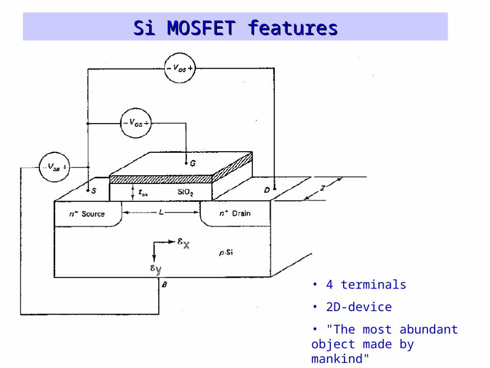
Si MOSFET featuresSi MOSFET features
• 4 terminals
• 2D-device
• "The most abundant object made by mankind"
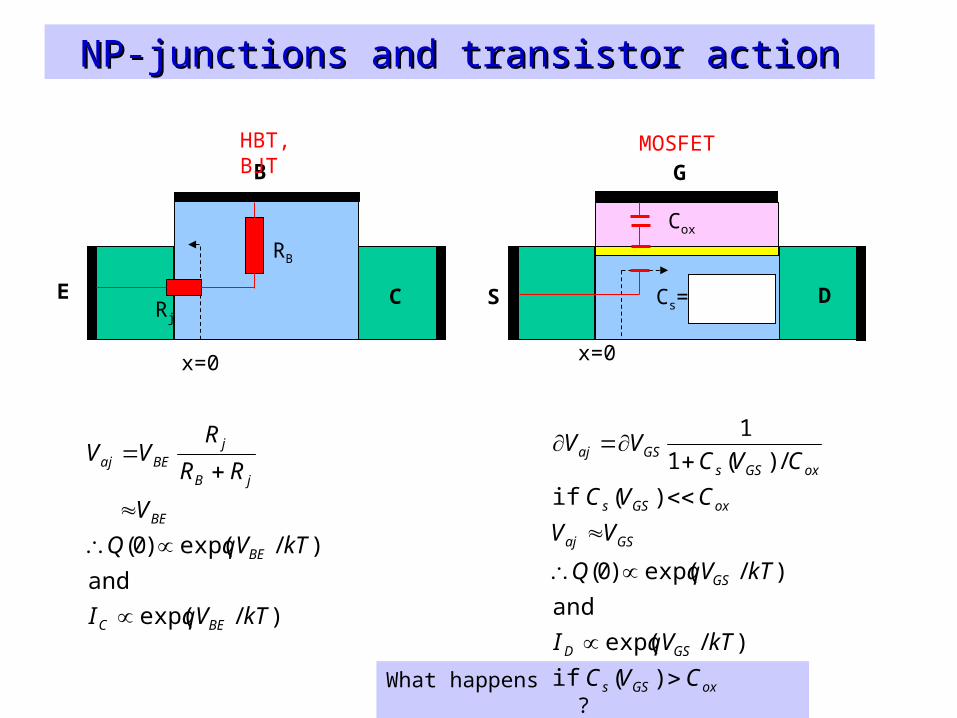
What happens ?
NP-junctions and transistor actionNP-junctions and transistor action
E
B G
S
RB
Rj
Cox
Cs=dQs/dVaj
HBT, BJT
MOSFET
)/exp(
and
)/exp()0(
kTqVI
kTqVQ
V
RR
RVV
BEC
BE
BE
jB
jBEaj
oxGSs
GSD
GS
GSaj
oxGSs
oxGSsGSaj
CVC
kTqVI
kTqVQ
VV
CVC
CVCVV
)( if
)/exp(
and
)/exp()0(
)( if
/)(1
1
x=0 x=0
DC
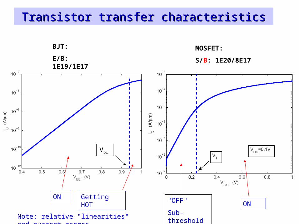
Transistor transfer characteristicsTransistor transfer characteristics
MOSFET:
S/B: 1E20/8E17
BJT:
E/B: 1E19/1E17
Vbi
ON Getting HOT
"OFF"
Sub-threshold
ON
Note: relative "linearities" and current ranges
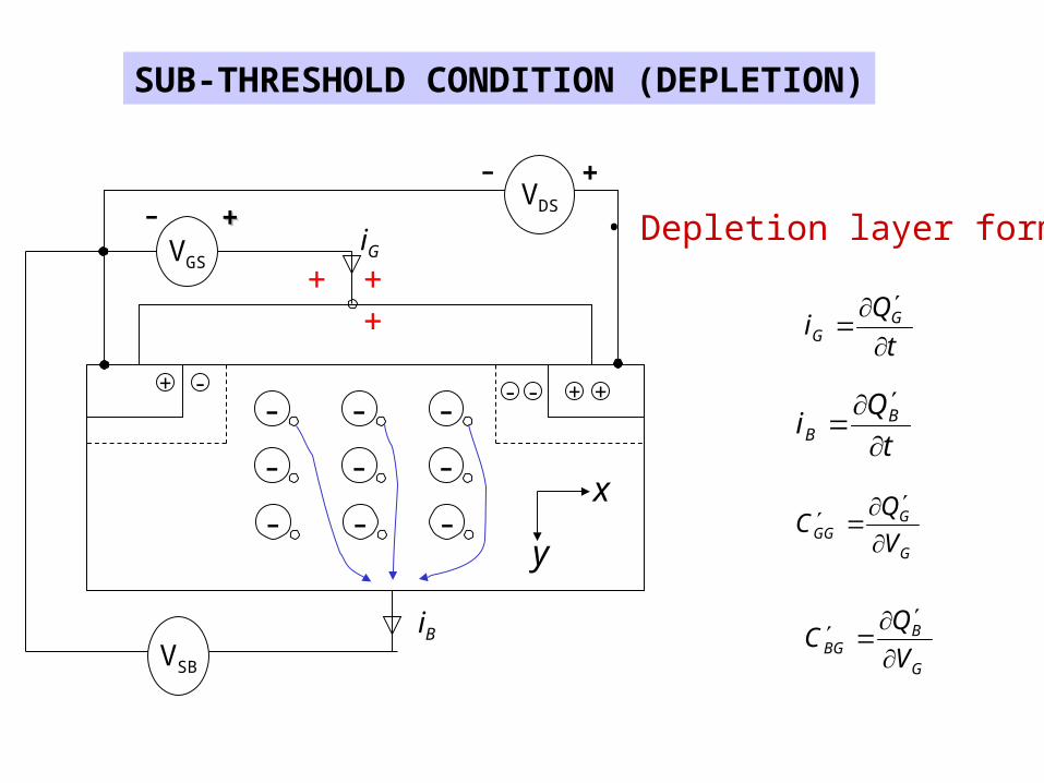
SUB-THRESHOLD CONDITION (DEPLETION)
- --
- --
- --y
x
+ + +- --
VSB
VGS
-+
iB
+ + +iG
-++
VDS
t
Qi BB
t
Qi GG
G
BBG V
QC
G
GGG V
QC
• Depletion layer forms
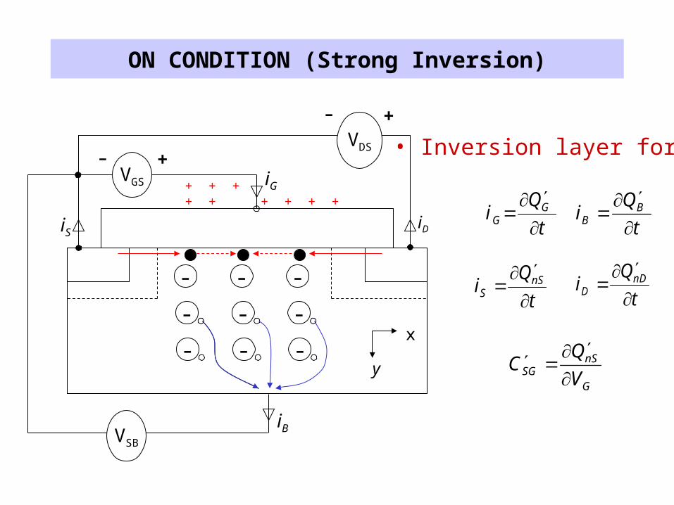
ON CONDITION (Strong Inversion)
- --
- --
- --
VSB
VGS
- +
iB
iS iD
iG+ + + ++ + + + +
+-
y
t
Qi GG
t
Qi BB
t
Qi nSS
t
Qi nDD
• Inversion layer forms
G
nSSG V
QC
VDS
x
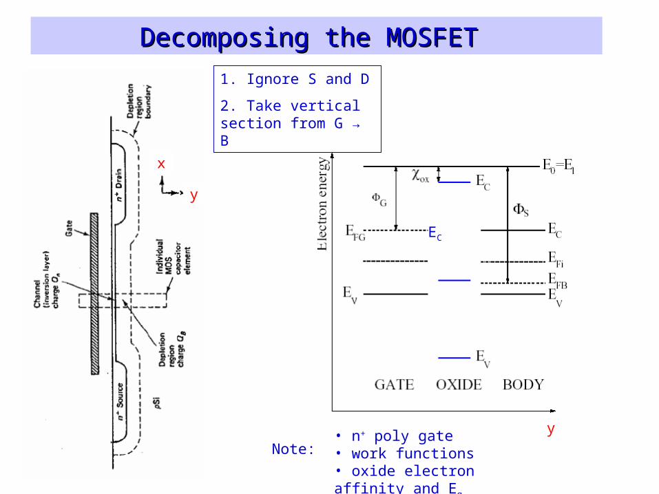
Decomposing the MOSFET Decomposing the MOSFET
Note:• n+ poly gate• work functions• oxide electron affinity and Eg
1. Ignore S and D
2. Take vertical section from G → B
y
x
y
EC
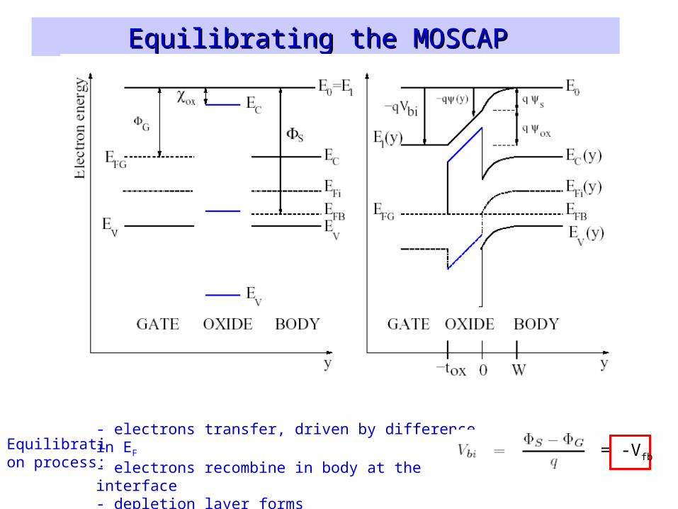
Equilibrating the MOSCAP Equilibrating the MOSCAP
Equilibration process:
- electrons transfer, driven by difference in EF
- electrons recombine in body at the interface- depletion layer forms- charge separation creates field in oxide
= -Vfb
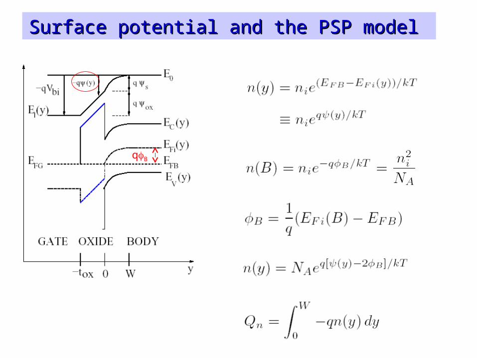
Surface potential and the PSP model Surface potential and the PSP model
qB
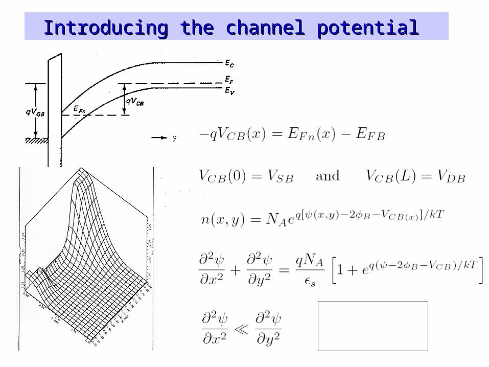
Introducing the channel potential Introducing the channel potential
THE GRADUAL CHANNEL APPROXIMATION
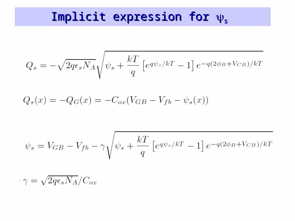
Implicit expression for Implicit expression for ss
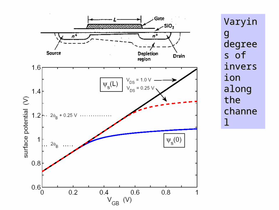
Varying Varying degrees degrees of of inversion inversion along the along the channelchannel
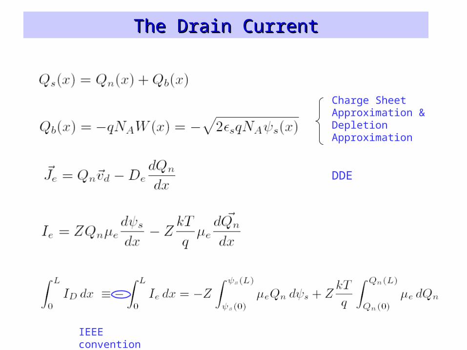
The Drain CurrentThe Drain Current
Charge Sheet Approximation & Depletion Approximation
DDE
IEEE convention
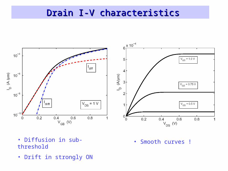
Drain I-V characteristicsDrain I-V characteristics
• Diffusion in sub-threshold
• Drift in strongly ON
• Smooth curves !
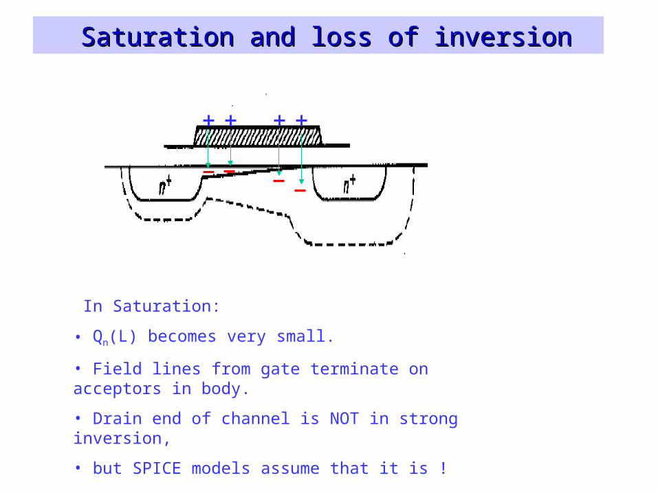
In Saturation:
• Qn(L) becomes very small.
• Field lines from gate terminate on acceptors in body.
• Drain end of channel is NOT in strong inversion,
• but SPICE models assume that it is !
Saturation and loss of inversionSaturation and loss of inversion
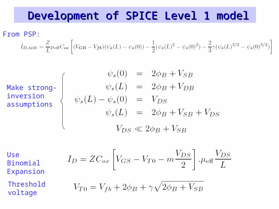
Development of SPICE Level 1 modelDevelopment of SPICE Level 1 model
From PSP:
Make strong-inversion assumptions
Use Binomial Expansion
Threshold voltage
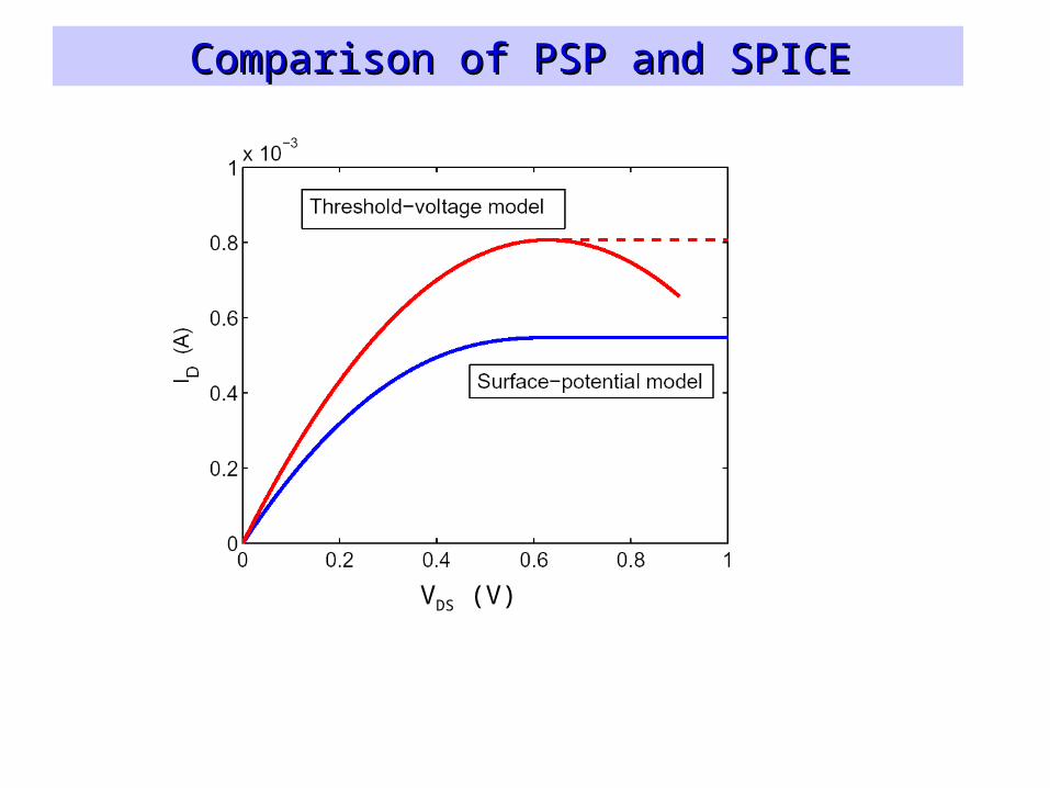
Comparison of PSP and SPICEComparison of PSP and SPICE
VDS (V)
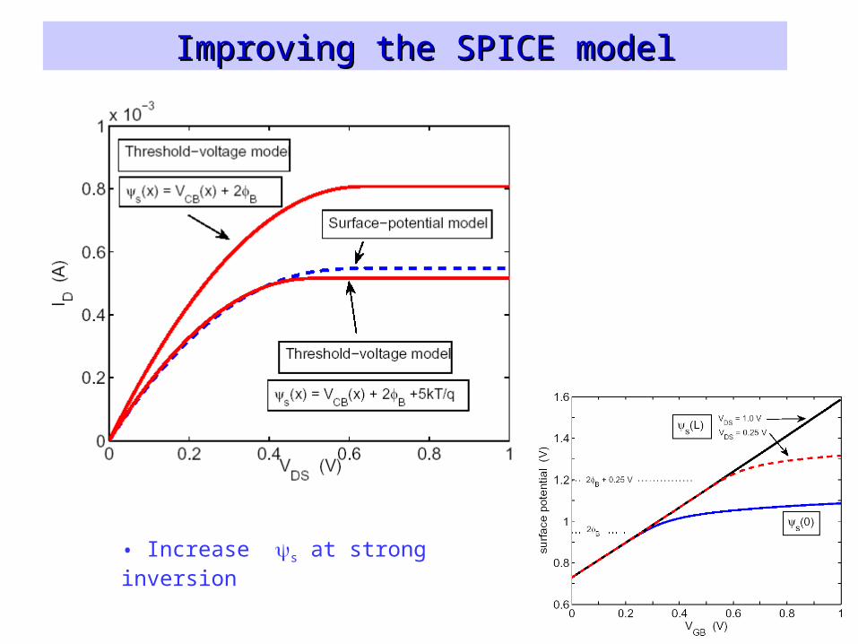
Improving the SPICE modelImproving the SPICE model
• Increase s at strong inversion
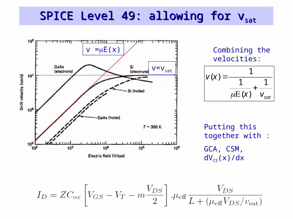
SPICE Level 49: allowing for vSPICE Level 49: allowing for vsat sat
v =E(x)
v=vsat
satvx
xv1
)(
11
)(
Combining the velocities:
Putting this together with :
GCA, CSM, dVCS(x)/dx
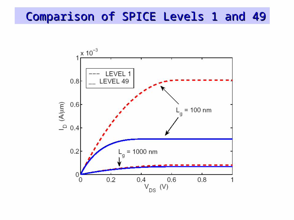
Comparison of SPICE Levels 1 and 49Comparison of SPICE Levels 1 and 49
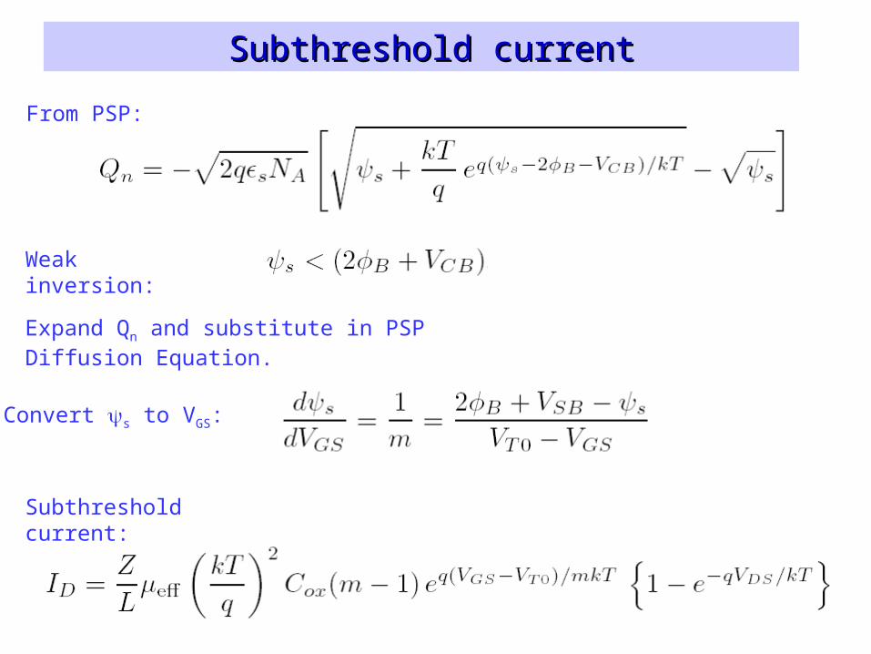
Subthreshold currentSubthreshold current
From PSP:
Weak inversion:
Expand Qn and substitute in PSP Diffusion Equation.
Convert s to VGS:
Subthreshold current:
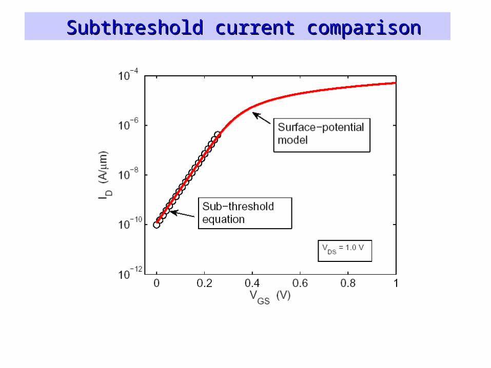
Subthreshold current comparisonSubthreshold current comparison
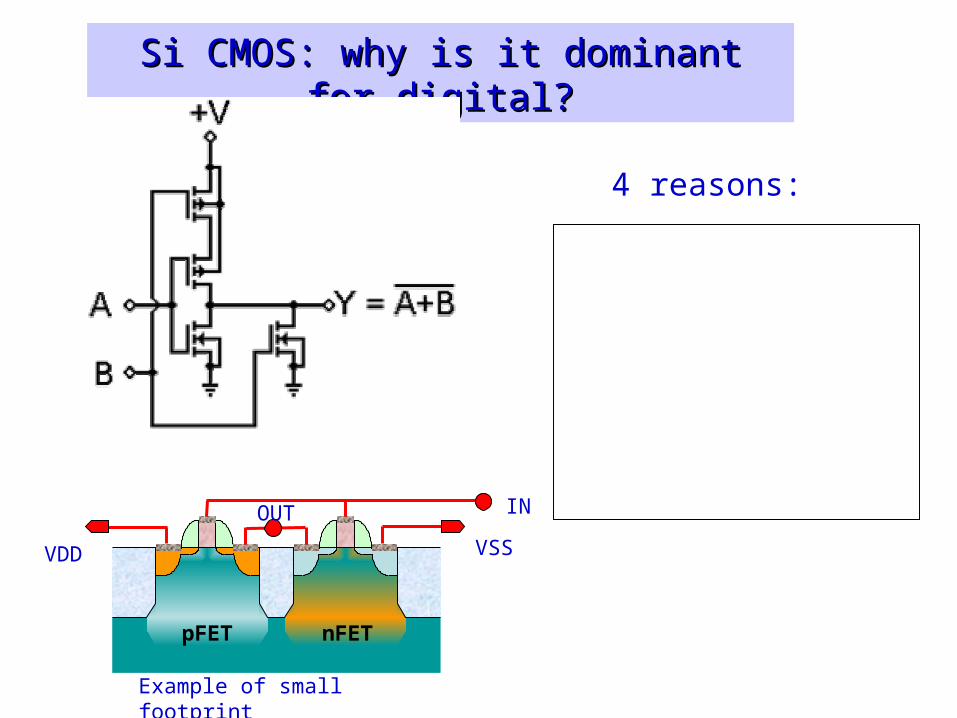
Si CMOS: why is it dominant for Si CMOS: why is it dominant for digital?digital?
4 reasons:
1. "Low" OFF current.
2. Compact logic: few transistors and no level shifting.
3. Small footprint.
4. Industrial investment.
pFET nFET
VSSVDD
INOUT
Example of small footprint
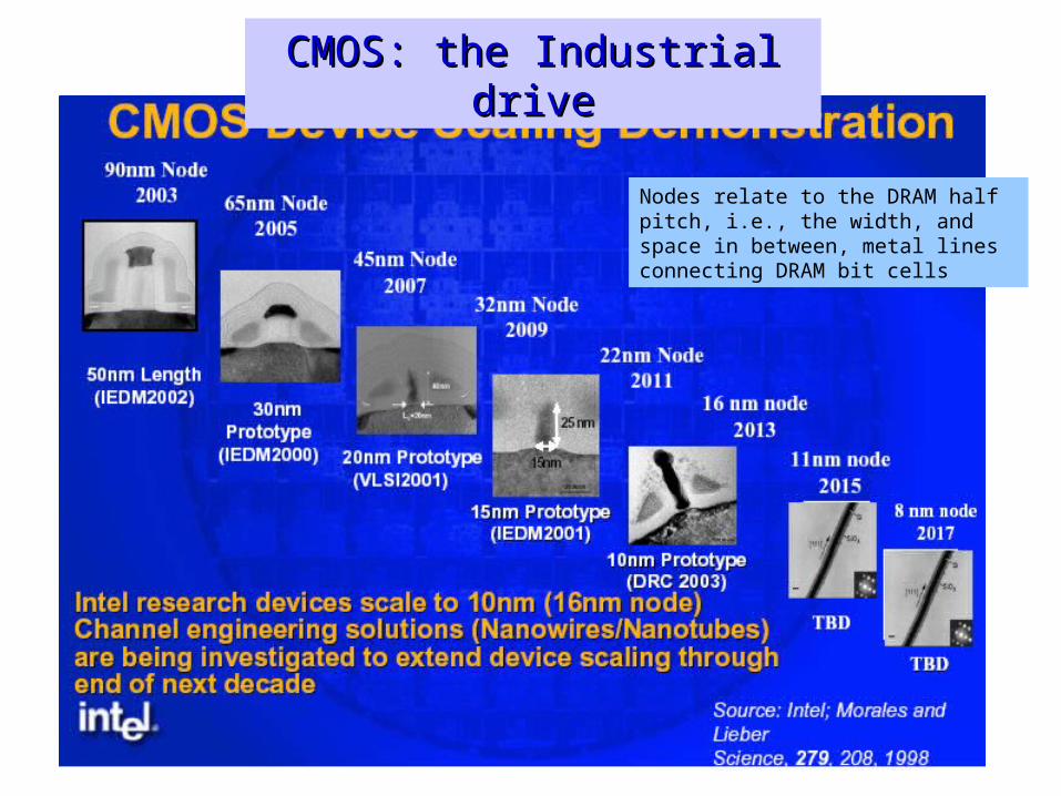
CMOS: the Industrial driveCMOS: the Industrial drive
Nodes relate to the DRAM half pitch, i.e., the width, and space in between, metal lines connecting DRAM bit cells
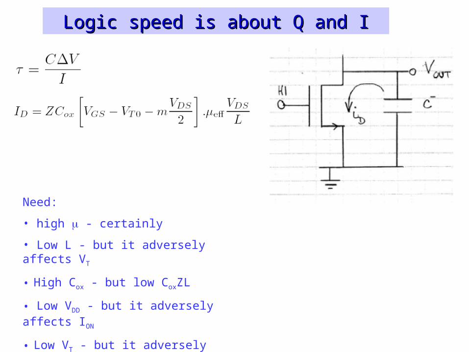
Logic speed is about Q and ILogic speed is about Q and I
Need:
• high - certainly
• Low L - but it adversely affects VT
• High Cox - but low CoxZL
• Low VDD - but it adversely affects ION
• Low VT - but it adversely affects ISUBT
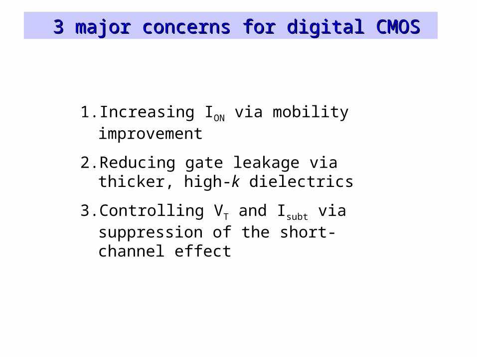
3 major concerns for digital CMOS3 major concerns for digital CMOS
1. Increasing ION via mobility improvement
2. Reducing gate leakage via thicker, high-k dielectrics
3. Controlling VT and Isubt via suppression of the short-channel effect
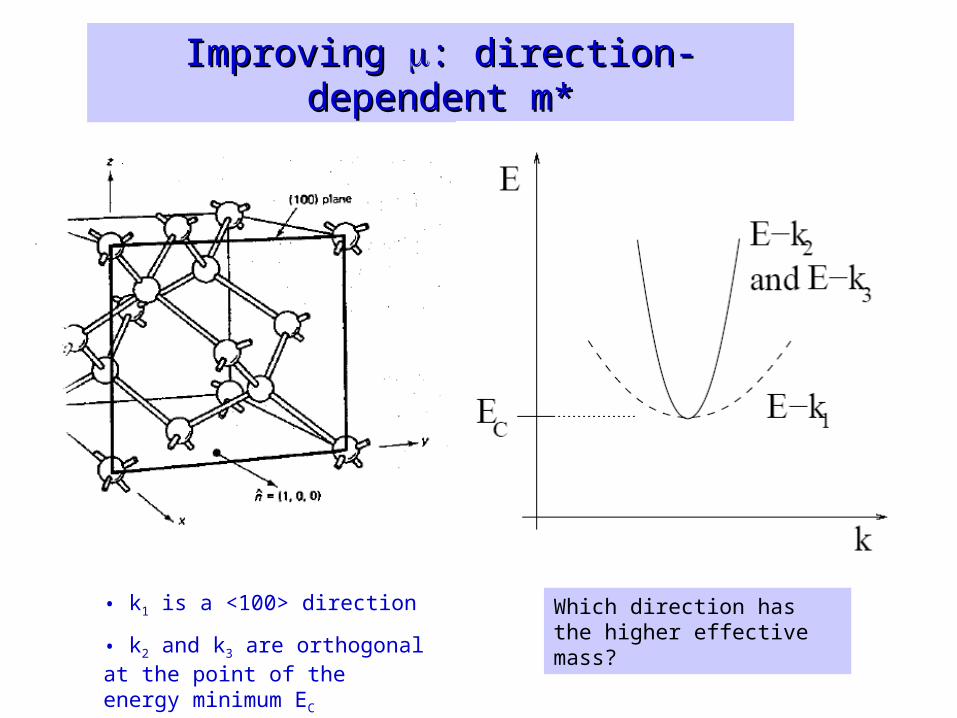
Improving Improving : direction-dependent : direction-dependent m*m*
• k1 is a <100> direction
• k2 and k3 are orthogonal at the point of the energy minimum EC
Which direction has the higher effective mass?
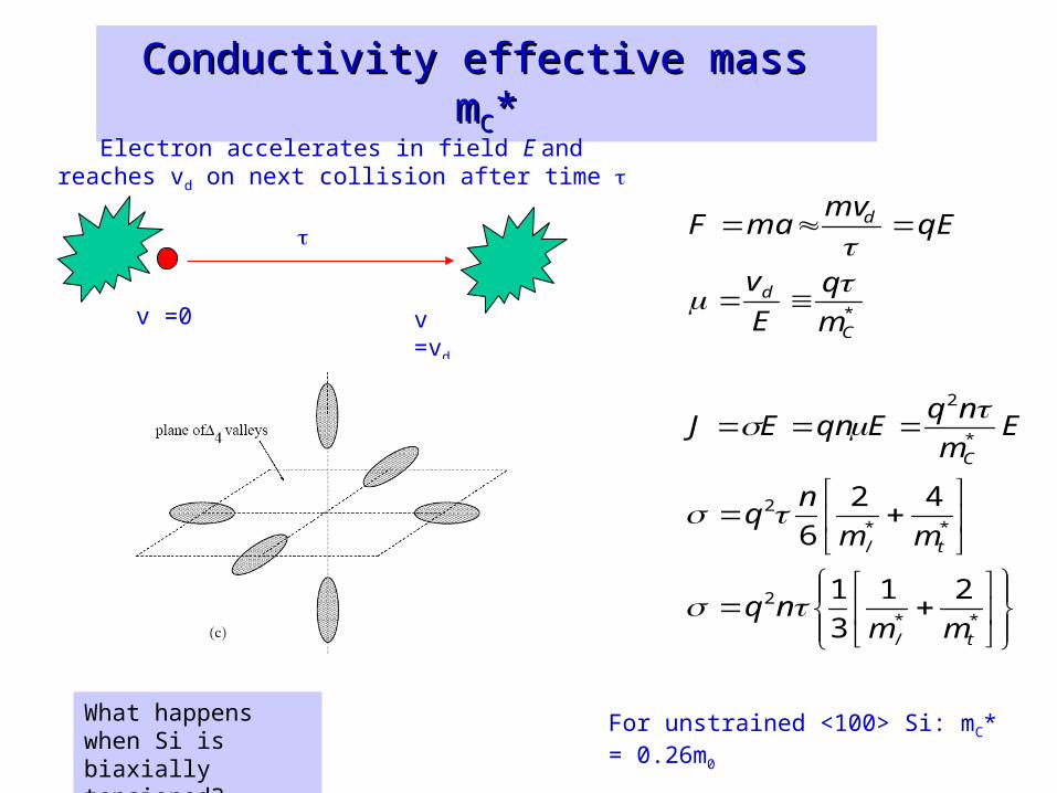
Conductivity effective mass mConductivity effective mass mCC**
Electron accelerates in field E and reaches vd on next collision after time
v =0 v =vd
**/
2
**/
2
*
2
*
21
3
1
42
6
t
t
C
C
d
d
mmnq
mm
nq
Em
nqEqnEJ
m
q
E
v
qEmv
maF
For unstrained <100> Si: mC* = 0.26m0
What happens when Si is biaxially tensioned?
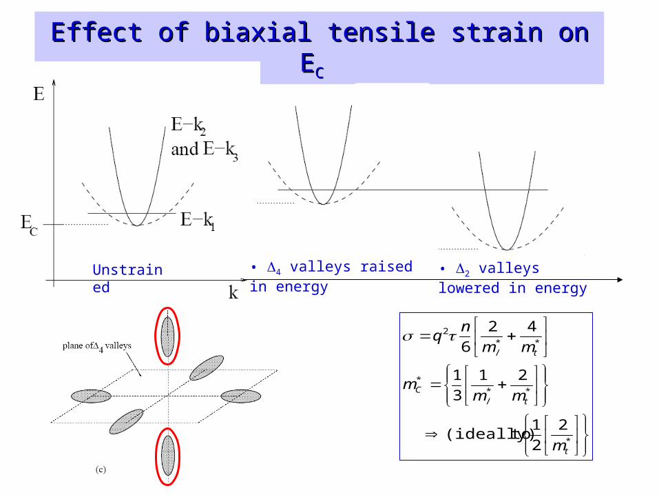
Effect of biaxial tensile strain on EEffect of biaxial tensile strain on ECC
• 4 valleys raised in energy
• 2 valleys lowered in energy
*
**/
*
**/
2
2
2
1 to(ideally)
21
3
1
42
6
t
tC
t
m
mmm
mm
nq
Unstrained
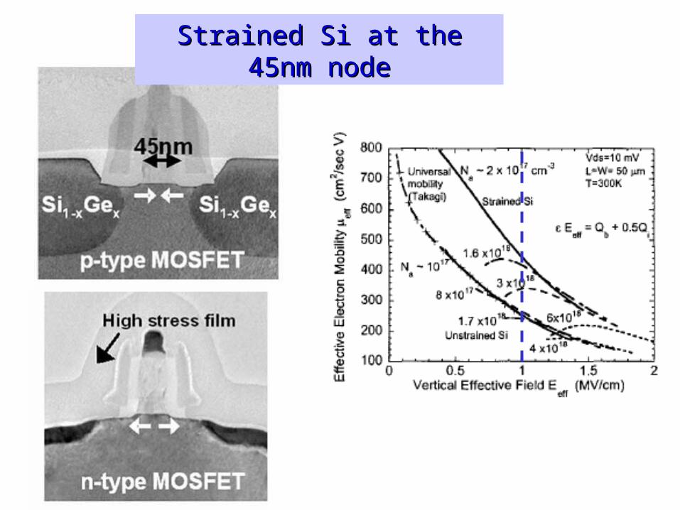
Strained Si at the 45nm Strained Si at the 45nm nodenode
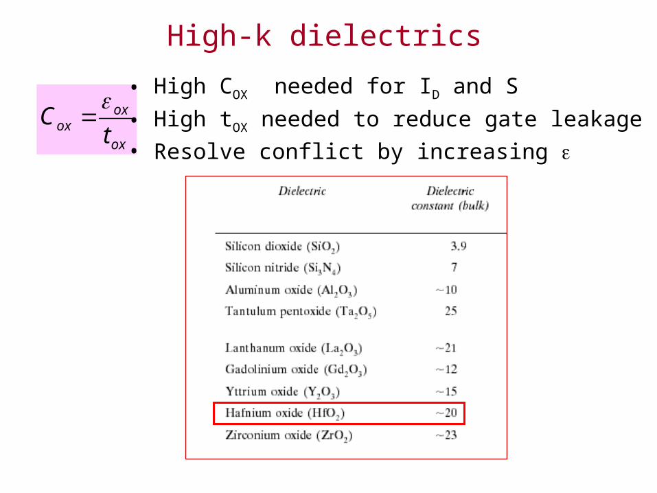
High-k dielectrics
ox
oxox tC
• High COX needed for ID and S
• High tOX needed to reduce gate leakage
• Resolve conflict by increasing
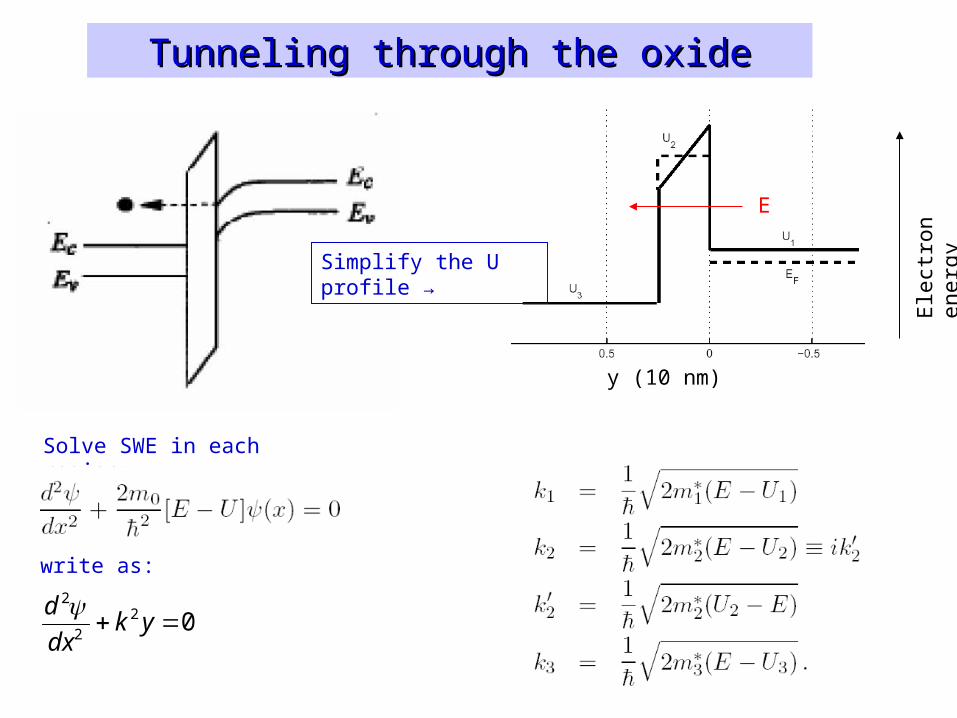
Tunneling through the oxideTunneling through the oxide
y (10 nm)
Ele
ctro
n en
ergy
E
Simplify the U profile →
Solve SWE in each region:
022
2
ykdx
d write as:
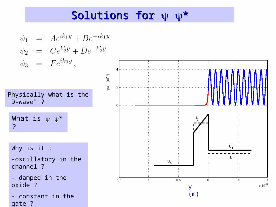
Solutions for Solutions for **
What is * ?* ?
Why is it :
-oscillatory in the channel ?
- damped in the oxide ?
- constant in the gate ?
Physically what is the "D-wave" ?
y (m)
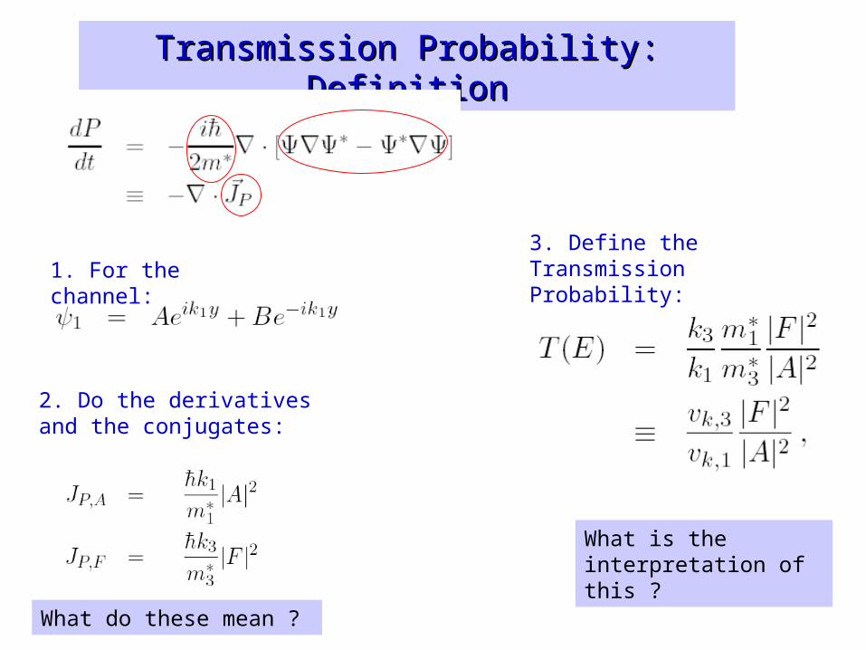
Transmission Probability: DefinitionTransmission Probability: Definition
1. For the channel:
2. Do the derivatives and the conjugates:
3. Define the Transmission Probability:
What do these mean ?
What is the interpretation of this ?
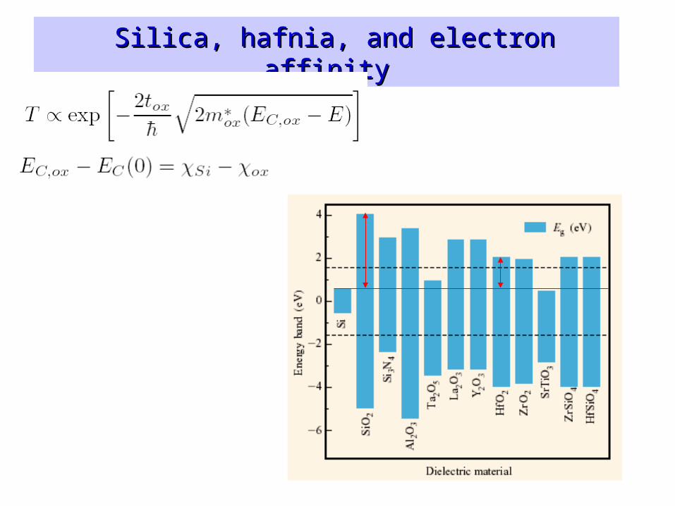
Silica, hafnia, and electron affinitySilica, hafnia, and electron affinity
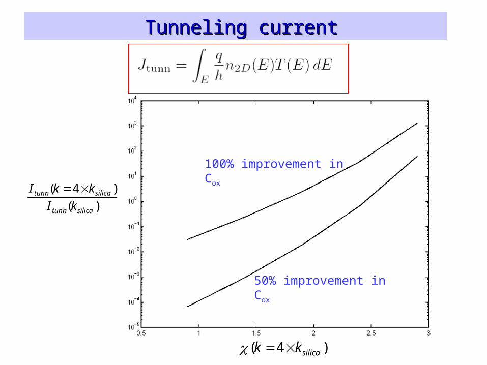
Tunneling currentTunneling current
)(
)4(
silicatunn
silicatunn
kI
kkI
)4( silicakk
100% improvement in Cox
50% improvement in Cox
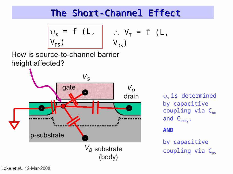
The Short-Channel EffectThe Short-Channel Effect
s = f (L, VDS) VT = f (L, VDS)
s is determined by capacitive coupling via Cox and Cbody,
AND
by capacitive coupling
via CDS
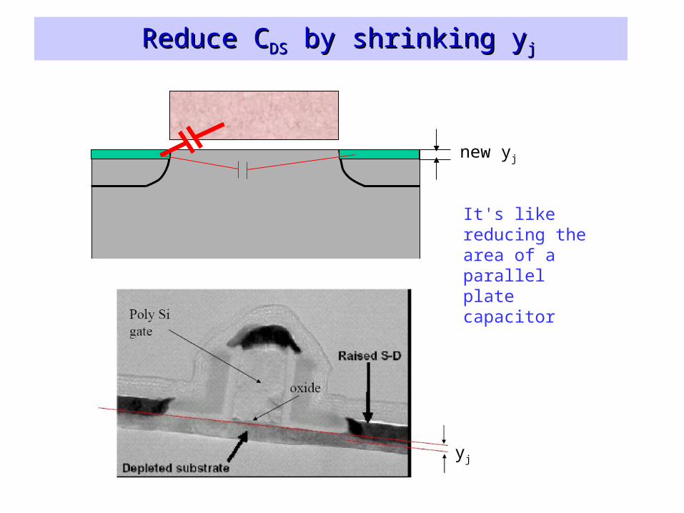
Reduce CReduce CDSDS by shrinking y by shrinking yjj
new yj
It's like reducing the area of a parallel plate capacitor
yj
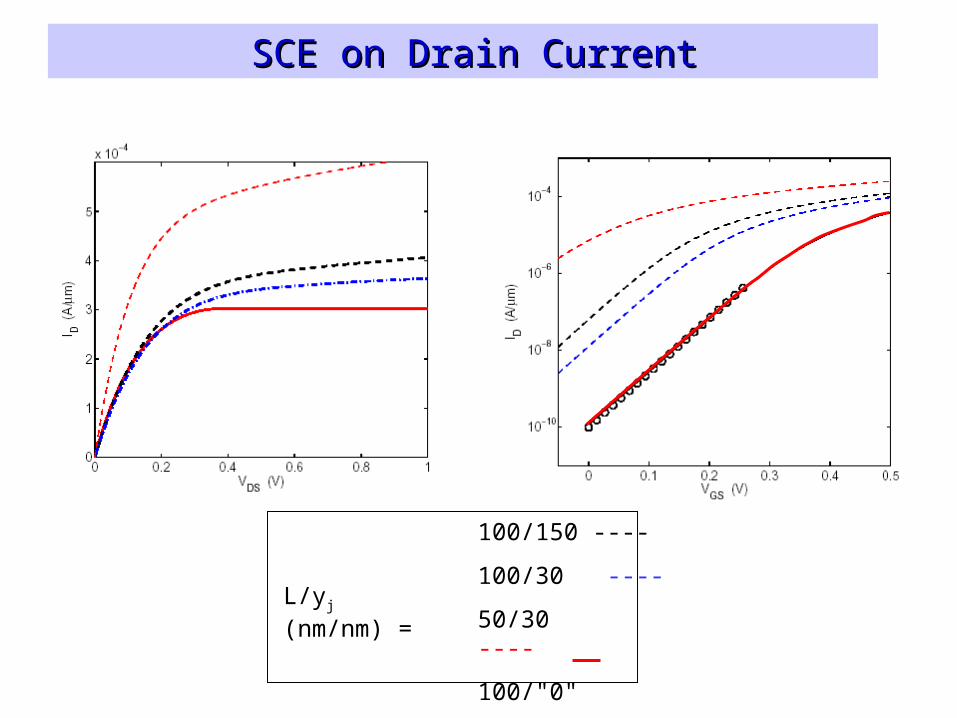
SCE on Drain CurrentSCE on Drain Current
L/yj (nm/nm) =
100/150 ----
100/30 ----
50/30 ----
100/"0"
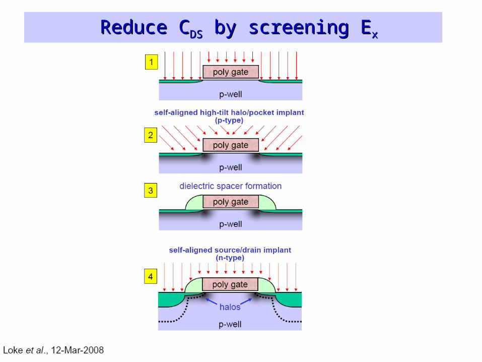
Reduce CReduce CDSDS by screening E by screening Exx
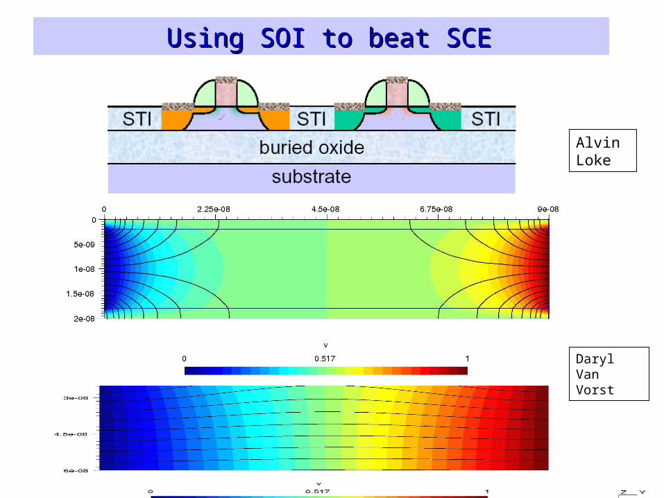
Using SOI to beat SCEUsing SOI to beat SCE
Daryl Van Vorst
Alvin Loke