Embed Size (px)
Citation preview
Modular, Scalable Computing for Systems with Tight SWaP Constraints
Prepared by Colorado Engineering, Inc.for HPEC 2011September 21, 2011
SBIR DATA RIGHTS
Contractor Name: Colorado Engineering Inc. (CEI)Contractor Address: 1310 United Heights, Suite 105, Colorado Springs, CO 80921Expiration of SBIR Data Rights: Expires 5 years after completion of project work for this or any follow-on SBIR contract, whichever is later.
This presentation contains data developed by Colorado Engineering under SBIR contract HQ0006-08-C-7908. The Government’s rights to use, modify, reproduce, release, perform, display, or disclose technical data or computer software marked with this legend are restricted during the period shown as provided in paragraph (b)(4) of the Rights in Noncommercial Technical Data and Computer Software - Small Business Innovation Research (SBIR) Program clause contained in the above identified contract. No restrictions apply after the expiration date shown above. Any reproduction of technical data, computer software, or portions thereof marked with this legend must also reproduce the markings.
Export or re-export of CEI products may be subject to restrictions and requirements of US export laws and regulations and may require advance authorization from the US Government.
Copyright © Colorado Engineering Inc. 2011. All Rights Reserved.
2Use or disclosure of data contained on this sheet is subject to the restrictions listed on the title page.
Outline
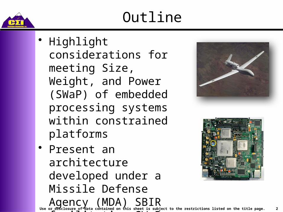
• Highlight considerations for meeting Size, Weight, and Power (SWaP) of embedded processing systems within constrained platforms
• Present an architecture developed under a Missile Defense Agency (MDA) SBIR facilitating SWaP-optimized solutions
3Use or disclosure of data contained on this sheet is subject to the restrictions listed on the title page.
Meeting SWaP Challenges
• Suggests need for optimized system solutions
• Engineer should have flexibility to address size, weight, and power in trade space
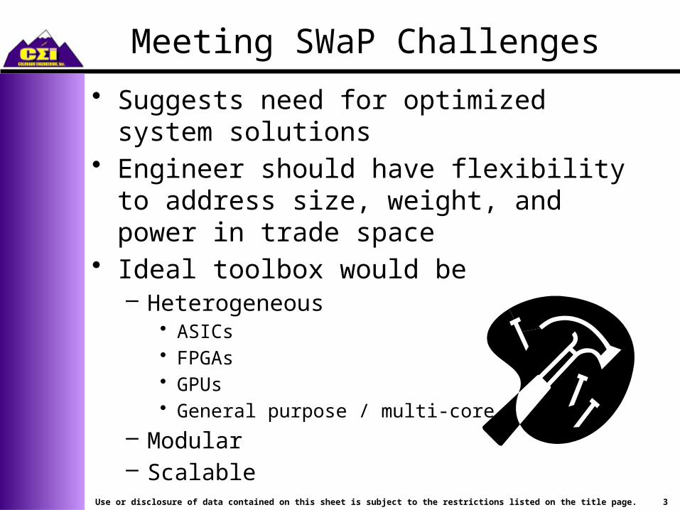
• Ideal toolbox would be– Heterogeneous
• ASICs• FPGAs• GPUs• General purpose / multi-core
– Modular– Scalable
4Use or disclosure of data contained on this sheet is subject to the restrictions listed on the title page.
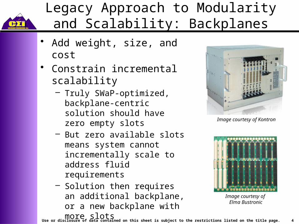
Legacy Approach to Modularity and Scalability: Backplanes
• Add weight, size, and cost• Constrain incremental
scalability– Truly SWaP-optimized,
backplane-centric solution should have zero empty slots
– But zero available slots means system cannot incrementally scale to address fluid requirements
– Solution then requires an additional backplane, or a new backplane with more slots
• Bottom line: backplanes are not SWaP friendly
Image courtesy of Kontron
Image courtesy of Elma Bustronic
5Use or disclosure of data contained on this sheet is subject to the restrictions listed on the title page.
Out-of-the-Box Approach to Embedded Computing for SWaP
• CEI and the Navy, sponsored by MDA, defined an open approach to SWaP-friendly embedded computing architectures– NRL– NSWC– ONR
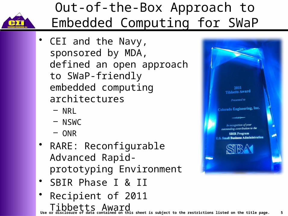
• RARE: Reconfigurable Advanced Rapid-prototyping Environment
• SBIR Phase I & II• Recipient of 2011 Tibbetts Award• No backplane!
6Use or disclosure of data contained on this sheet is subject to the restrictions listed on the title page.
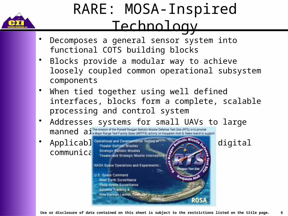
RARE: MOSA-Inspired Technology• Decomposes a general sensor system into functional COTS
building blocks• Blocks provide a modular way to achieve loosely coupled
common operational subsystem components• When tied together using well defined interfaces, blocks form
a complete, scalable processing and control system• Addresses systems for small UAVs to large manned aircraft• Applicable to radar, -INT, EW, and digital communications
ROSAROSA
Modularity, Scalability, and Flexibility
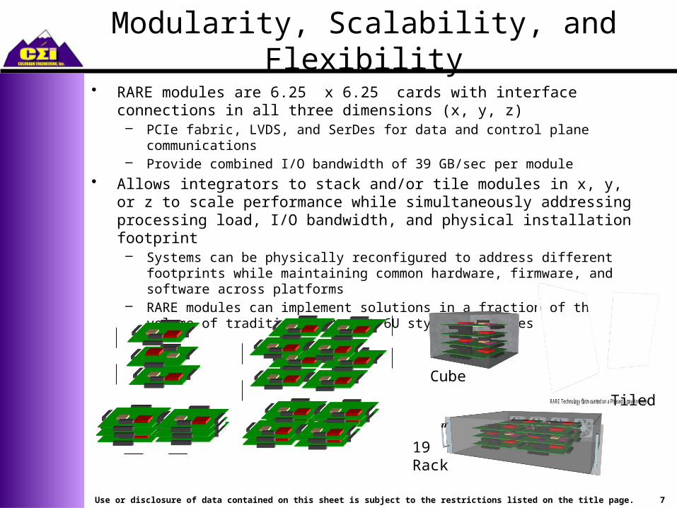
• RARE modules are 6.25” x 6.25” cards with interface connections in all three dimensions (x, y, z)– PCIe fabric, LVDS, and SerDes for data and control plane communications– Provide combined I/O bandwidth of 39 GB/sec per module
• Allows integrators to stack and/or tile modules in x, y, or z to scale performance while simultaneously addressing processing load, I/O bandwidth, and physical installation footprint– Systems can be physically reconfigured to address different footprints while
maintaining common hardware, firmware, and software across platforms– RARE modules can implement solutions in a fraction of the volume of traditional 20-
slot 6U style backplanes
RARE Technology flat mounted on a Phased Array Antenna
19” Rack
Cube
Tiled
7Use or disclosure of data contained on this sheet is subject to the restrictions listed on the title page.
Module Examples
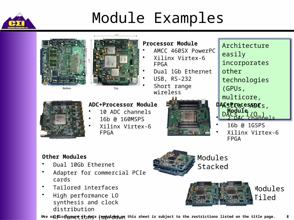
Processor Module• AMCC 460SX PowerPC• Xilinx Virtex-6 FPGA• Dual 1Gb Ethernet• USB, RS-232• Short range wireless
Architecture easily incorporates other technologies (GPUs, multicore, ASICs, ADCs, DACs, I/O…)
Architecture easily incorporates other technologies (GPUs, multicore, ASICs, ADCs, DACs, I/O…)
Modules Tiled
Modules Stacked
ADC+Processor Module• 10 ADC channels • 16b @ 160MSPS• Xilinx Virtex-6 FPGA
DAC+Processor Module• 2 DAC channels• 16b @ 1GSPS• Xilinx Virtex-6 FPGA
Other Modules• Dual 10Gb Ethernet• Adapter for commercial PCIe cards• Tailored interfaces• High performance LO synthesis and
clock distribution• RF functions (up/down conversion)
8Use or disclosure of data contained on this sheet is subject to the restrictions listed on the title page.
Heterogeneous Processing
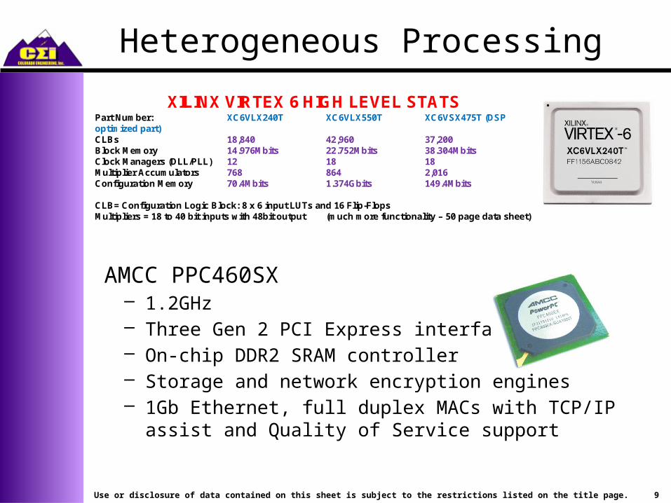
XILINX VIRTEX 6 HIGH LEVEL STATSPart Number: XC6VLX240T XC6VLX550T XC6VSX475T (DSP optimized part)CLBs 18,840 42,960 37,200Block Memory 14.976Mbits 22.752Mbits 38.304MbitsClock Managers (DLL/PLL) 12 18 18Multiplier Accumulators 768 864 2,016Configuration Memory 70.4Mbits 1.374Gbits 149.4Mbits
CLB= Configuration Logic Block: 8 x 6 input LUTs and 16 Flip-FlopsMultipliers = 18 to 40 bit inputs with 48bit output (much more functionality – 50 page data sheet)
AMCC PPC460SX– 1.2GHz– Three Gen 2 PCI Express interfaces– On-chip DDR2 SRAM controller– Storage and network encryption engines– 1Gb Ethernet, full duplex MACs with TCP/IP assist and
Quality of Service support
9Use or disclosure of data contained on this sheet is subject to the restrictions listed on the title page.
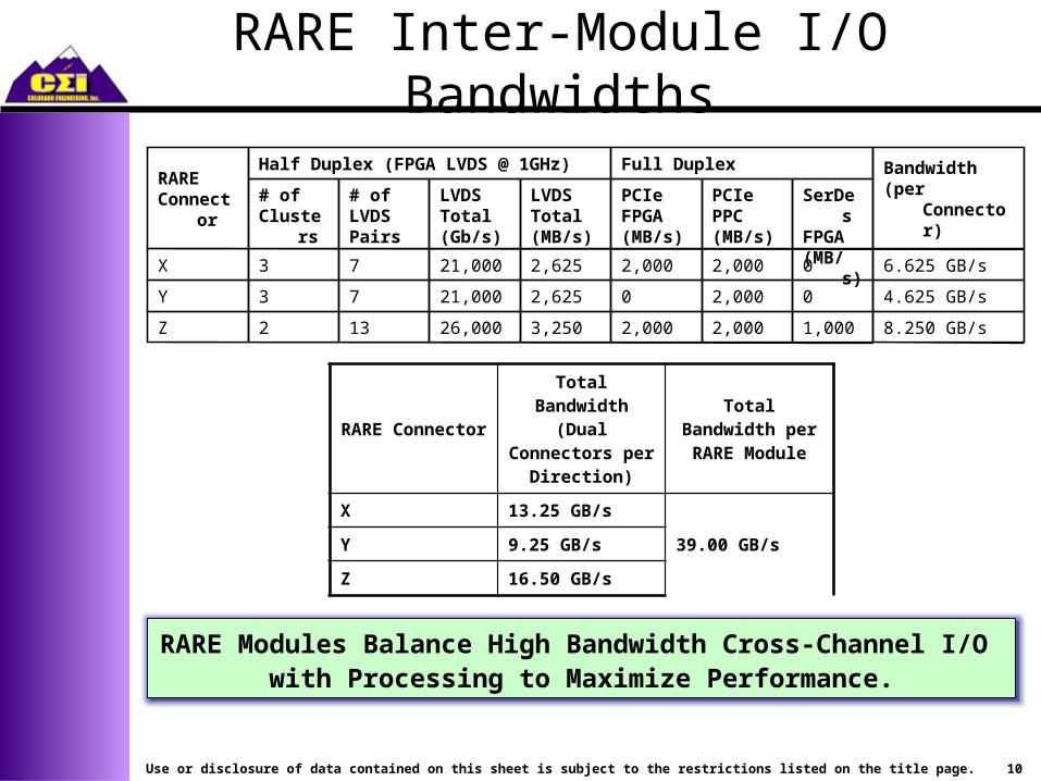
RARE Inter-Module I/O Bandwidths
8.250 GB/s1,0002,0002,0003,25026,000132Z
4.625 GB/s02,00002,62521,00073Y
6.625 GB/s02,0002,0002,62521,00073X
SerDesFPGA(MB/s)
PCIePPC(MB/s)
PCIeFPGA(MB/s)
LVDSTotal(MB/s)
LVDSTotal(Gb/s)
# ofLVDSPairs
# of Clusters
Bandwidth(per Connector)
Full DuplexHalf Duplex (FPGA LVDS @ 1GHz)
RAREConnector
RARE ConnectorTotal Bandwidth (Dual Connectors
per Direction)
Total Bandwidth per RARE Module
X 13.25 GB/s
39.00 GB/sY 9.25 GB/s
Z 16.50 GB/s
10Use or disclosure of data contained on this sheet is subject to the restrictions listed on the title page.
RARE Modules Balance High Bandwidth Cross-Channel I/O with Processing to Maximize Performance.
RARE Modules Balance High Bandwidth Cross-Channel I/O with Processing to Maximize Performance.
FPGA
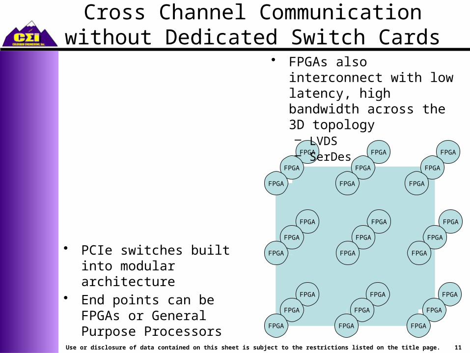
• PCIe switches built into modular architecture
• End points can be FPGAs or General Purpose Processors
FPGA
FPGA
FPGA
FPGA
FPGA
FPGA
FPGA
FPGA
FPGA
FPGA
FPGA
FPGA
FPGA
FPGA
FPGA
FPGA
FPGA
FPGA
FPGA
FPGA
FPGA
FPGA
FPGA
FPGA
FPGA
FPGA
• FPGAs also interconnect with low latency, high bandwidth across the 3D topology– LVDS– SerDes
Cross Channel Communication without Dedicated Switch Cards
11Use or disclosure of data contained on this sheet is subject to the restrictions listed on the title page.
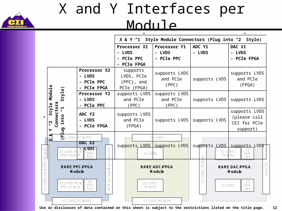
X and Y Interfaces per Module
RARE PPC/FPGAModule
X1:
LV
DS
; PC
Ie P
PC
; PC
Ie V
6 X2: LV
DS
; PC
Ie PP
C; P
CIe V
6
Z1: LVDS; PCIe PPC; PCIe V6
Z3: SER-DES
Z2: LVDS; PCIe PPC; PCIe V6
Z4: SER-DES
Y1: LVDS; PCIe PPC
Y2: LVDS; PCIe PPC
RARE ADC/FPGAModule
Z1: LVDS
Z2: LVDS; PCIe V6
Y1: LVDS
Y2: LVDS; PCIe V6
RARE DAC/FPGAModule
X1:
LV
DS
; PC
Ie V
6
X2: LV
DS
Z1: LVDS; PCIe V6
Z3: SER-DES
Z2: LVDSZ4:
SER-DES
X & Y “1” Style Module Connectors (Plug into “2” Style) Processor X1
- LVDS- PCIe PPC- PCIe FPGA
Processor Y1- LVDS- PCIe PPC
ADC Y1- LVDS
DAC X1- LVDS- PCIe FPGA
X & Y “2” Style
Module Connector
s (Plug into “1” Style)
Processor X2- LVDS- PCIe PPC- PCIe FPGA
supports LVDS, PCIe (PPC), and
PCIe (FPGA)
supports LVDS and PCIe (PPC)
supports LVDSsupports LVDS
and PCIe (FPGA)
Processor Y2- LVDS- PCIe PPC
supports LVDS and PCIe (PPC)
supports LVDS and PCIe (PPC)
supports LVDS supports LVDS
ADC Y2- LVDS- PCIe FPGA
supports LVDS and PCIe (FPGA)
supports LVDS supports LVDSsupports LVDS(please call CEI
for PCIe support)DAC X2- LVDS
supports LVDS supports LVDS supports LVDS supports LVDS
12Use or disclosure of data contained on this sheet is subject to the restrictions listed on the title page.
Z Interfaces per Module
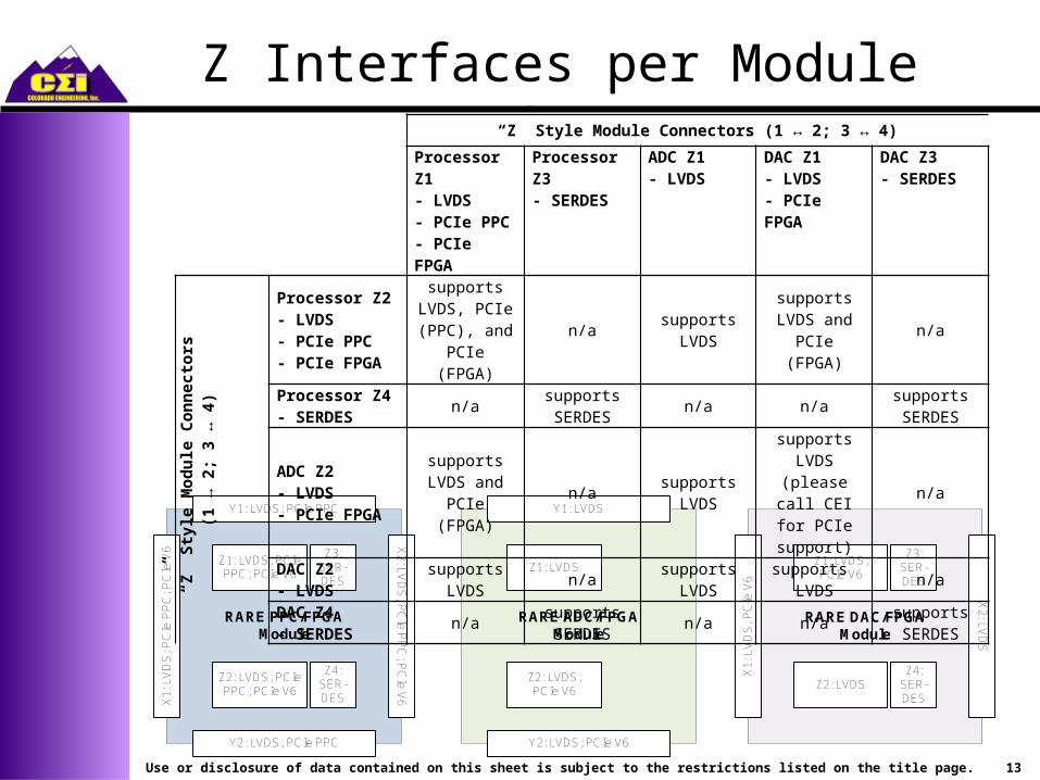
RARE PPC/FPGAModule
X1:
LV
DS
; PC
Ie P
PC
; PC
Ie V
6 X2: LV
DS
; PC
Ie PP
C; P
CIe V
6
Z1: LVDS; PCIe PPC; PCIe V6
Z3: SER-DES
Z2: LVDS; PCIe PPC; PCIe V6
Z4: SER-DES
Y1: LVDS; PCIe PPC
Y2: LVDS; PCIe PPC
RARE ADC/FPGAModule
Z1: LVDS
Z2: LVDS; PCIe V6
Y1: LVDS
Y2: LVDS; PCIe V6
RARE DAC/FPGAModule
X1:
LV
DS
; PC
Ie V
6
X2: LV
DS
Z1: LVDS; PCIe V6
Z3: SER-DES
Z2: LVDSZ4:
SER-DES
“Z” Style Module Connectors (1 ↔ 2; 3 ↔ 4)
Processor Z1- LVDS- PCIe PPC- PCIe FPGA
Processor Z3- SERDES
ADC Z1- LVDS
DAC Z1- LVDS- PCIe FPGA
DAC Z3- SERDES
“Z” Style
Module Connect
ors (1 ↔ 2; 3 ↔ 4)
Processor Z2- LVDS- PCIe PPC- PCIe FPGA
supports LVDS, PCIe (PPC), and
PCIe (FPGA)
n/a supports LVDSsupports LVDS
and PCIe (FPGA)
n/a
Processor Z4- SERDES
n/asupports SERDES
n/a n/asupports SERDES
ADC Z2- LVDS- PCIe FPGA
supports LVDS and PCIe (FPGA)
n/a supports LVDS
supports LVDS(please call
CEI for PCIe support)
n/a
DAC Z2- LVDS
supports LVDS n/a supports LVDSsupports
LVDSn/a
DAC Z4- SERDES
n/asupports SERDES
n/a n/asupports SERDES
13Use or disclosure of data contained on this sheet is subject to the restrictions listed on the title page.
14Use or disclosure of data contained on this sheet is subject to the restrictions listed on the title page.
Integrated Health and Status Monitoring
• I2C network of microcontrollers distributed throughout architecture for health and status– ADCs built into microcontrollers monitor voltages,
currents, and temperatures– Used to sequence power supplies and protect modules in
event of supply issues or overheating– Microcontrollers can shut down modules or system when
tolerances are not within defined limits
• Fully programmable and tailorable• More information available in poster session
15Use or disclosure of data contained on this sheet is subject to the restrictions listed on the title page.
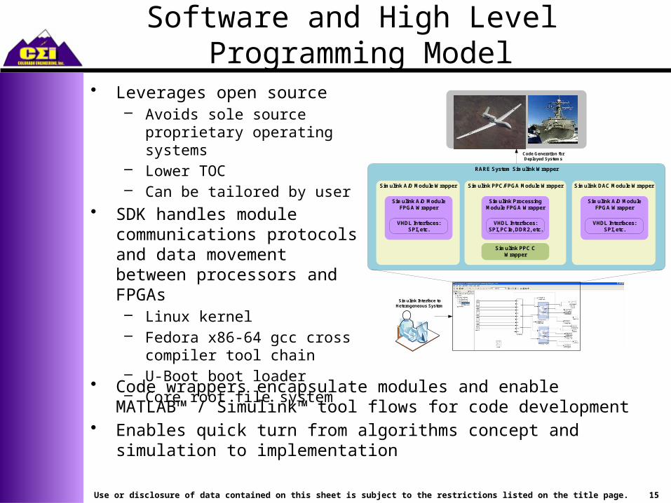
Software and High Level Programming Model
• Leverages open source– Avoids sole source proprietary
operating systems– Lower TOC– Can be tailored by user
• SDK handles module communications protocols and data movement between processors and FPGAs– Linux kernel– Fedora x86-64 gcc cross
compiler tool chain– U-Boot boot loader– Core root file system
RARE System Simulink Wrapper
Simulink PPC/FPGA Module WrapperSimulink A/D Module Wrapper
Simulink A/D Module FPGA Wrapper
Simulink Processing Module FPGA Wrapper
VHDL Interfaces: SPI, etc.
VHDL Interfaces: SPI, PCIe, DDR2, etc.
Code Generation for Deployed Systems
Simulink PPC C Wrapper
Simulink Interface to Heterogeneous System
Simulink DAC Module Wrapper
Simulink A/D Module FPGA Wrapper
VHDL Interfaces: SPI, etc.
• Code wrappers encapsulate modules and enable MATLAB™ / Simulink™ tool flows for code development
• Enables quick turn from algorithms concept and simulation to implementation
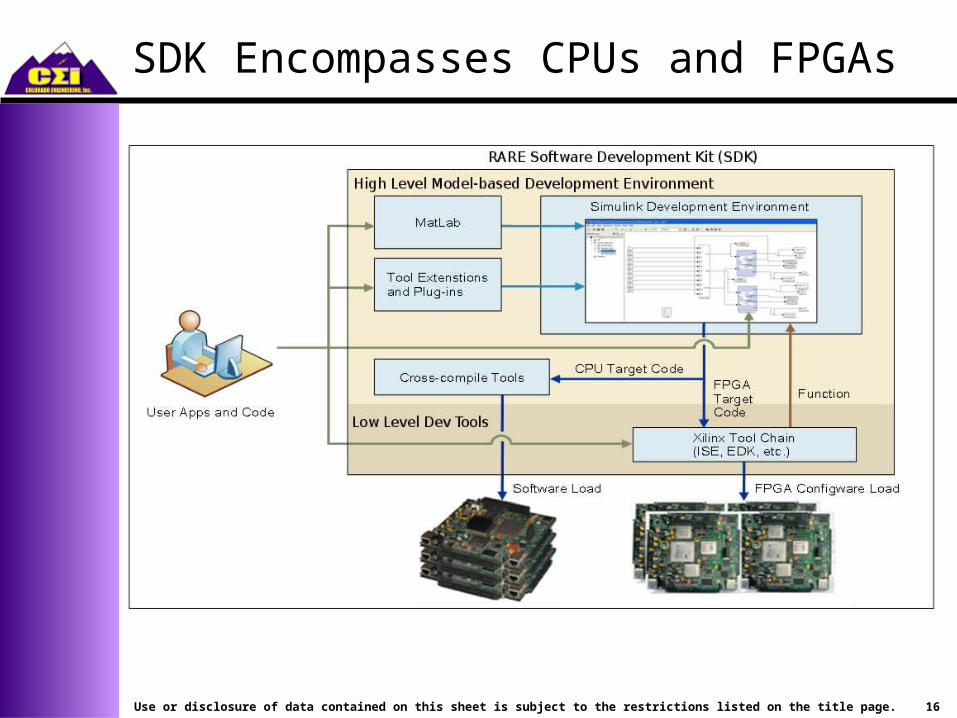
SDK Encompasses CPUs and FPGAs
16Use or disclosure of data contained on this sheet is subject to the restrictions listed on the title page.
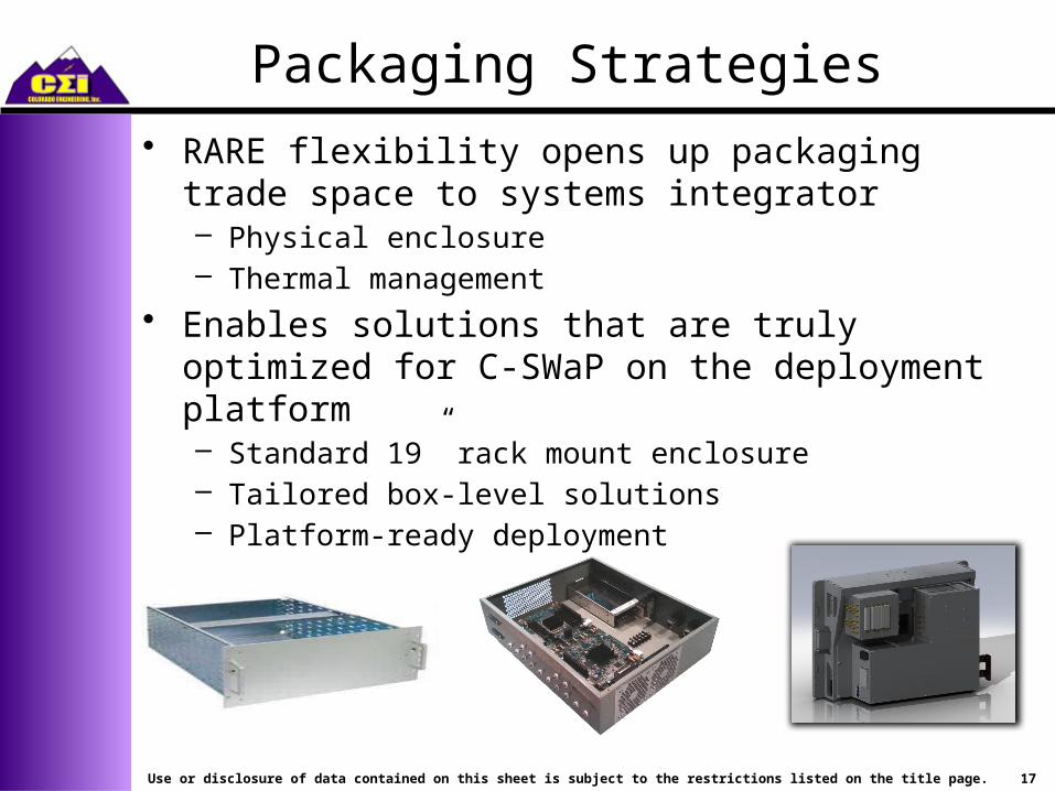
Packaging Strategies
• RARE flexibility opens up packaging trade space to systems integrator– Physical enclosure– Thermal management
• Enables solutions that are truly optimized for C-SWaP on the deployment platform– Standard 19” rack mount enclosure– Tailored box-level solutions– Platform-ready deployment
17Use or disclosure of data contained on this sheet is subject to the restrictions listed on the title page.
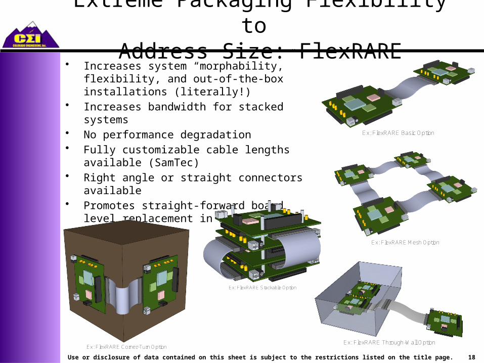
Extreme Packaging Flexibility to Address Size: FlexRARE
• Increases system “morphability,” flexibility, and out-of-the-box installations (literally!)
• Increases bandwidth for stacked systems• No performance degradation• Fully customizable cable lengths available
(SamTec)• Right angle or straight connectors available• Promotes straight-forward board level
replacement in mesh structure
Ex: FlexRARE Basic Option
Ex: FlexRARE Mesh Option
Ex: FlexRARE Stackable Option
Ex: FlexRARE Corner-Turn OptionEx: FlexRARE Through-Wall Option
18Use or disclosure of data contained on this sheet is subject to the restrictions listed on the title page.
19Use or disclosure of data contained on this sheet is subject to the restrictions listed on the title page.
Example Applications
• RARE architecture is being utilized by multiple DoD agencies to meet C-SWaP while adhering to MOSA philosophies
• Two examples– Programmable MIMO radar transmit / receive
system– Sense and Avoid radar for UAVs
20Use or disclosure of data contained on this sheet is subject to the restrictions listed on the title page.
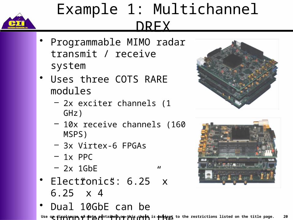
Example 1: Multichannel DREX
• Programmable MIMO radar transmit / receive system
• Uses three COTS RARE modules– 2x exciter channels (1 GHz)– 10x receive channels (160 MSPS)– 3x Virtex-6 FPGAs– 1x PPC– 2x 1GbE
• Electronics: 6.25” x 6.25” x 4”• Dual 10GbE can be supported
through the addition of one more module
21Use or disclosure of data contained on this sheet is subject to the restrictions listed on the title page.
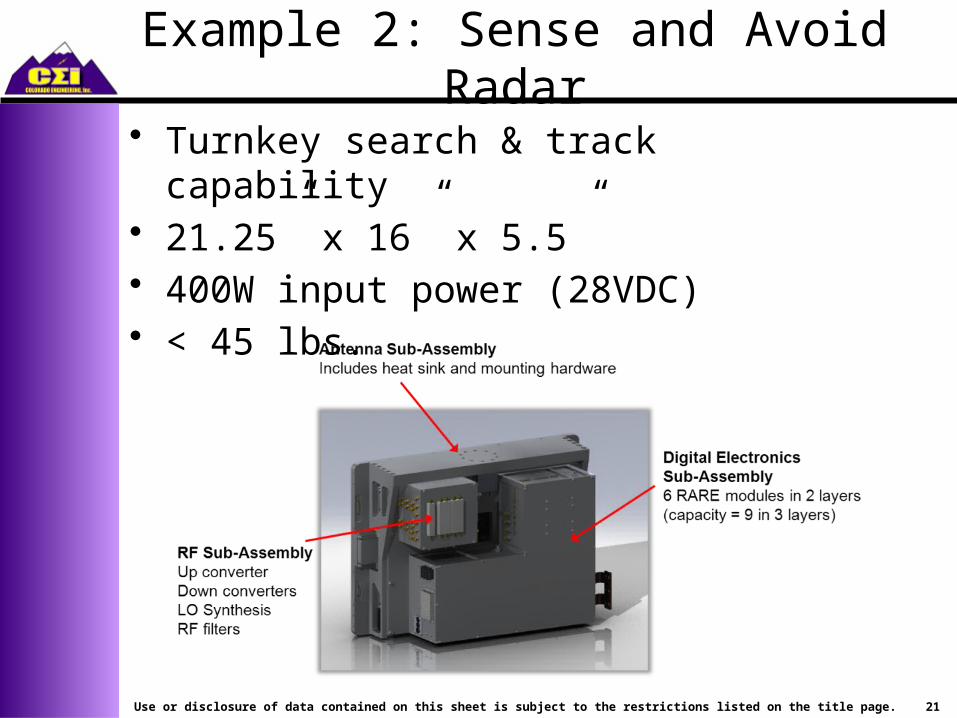
Example 2: Sense and Avoid Radar
• Turnkey search & track capability• 21.25” x 16” x 5.5”• 400W input power (28VDC)• < 45 lbs.
22Use or disclosure of data contained on this sheet is subject to the restrictions listed on the title page.
Summary• RARE facilitates embedded processing solutions for SWaP-
constrained applications– Heterogeneous technology helps balance processing capability
with power consumption– Solutions are not backplane constrained thus maximizing
flexibility within SWaP trade space– Architecture enables integrators to simultaneously address
processing capacity, I/O bandwidth, and physical installation footprint while eliminating the cost and impact of backplane and dedicated switch card architectures
– Model-based software development accelerates transition from algorithmic concept to deployment
• MOSA approach facilitates the realization of common subsystem building blocks and lowers total ownership costs
• Award winning technology being utilized in multiple DoD programs

Thank You!
For more information please contact:
Michael J. BonatoColorado Engineering, Inc.
[email protected] 719-388-8582 (office)
www.coloradoengineeringinc.com
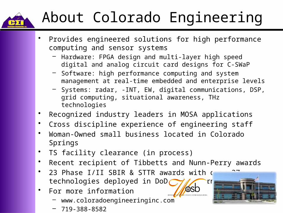
About Colorado Engineering• Provides engineered solutions for high performance computing and
sensor systems– Hardware: FPGA design and multi-layer high speed digital and analog
circuit card designs for C-SWaP – Software: high performance computing and system management at real-
time embedded and enterprise levels– Systems: radar, -INT, EW, digital communications, DSP, grid computing,
situational awareness, THz technologies• Recognized industry leaders in MOSA applications• Cross discipline experience of engineering staff• Woman-Owned small business located in Colorado Springs• TS facility clearance (in process)• Recent recipient of Tibbetts and Nunn-Perry awards• 23 Phase I/II SBIR & STTR awards with over 37 technologies
deployed in DoD and Government systems• For more information
– www.coloradoengineeringinc.com– 719-388-8582