Embed Size (px)
Citation preview
ROBERT HENDRY, GILBERT HENDRY, KEREN BERGMAN
LIGHTWAVE RESEARCH LABCOLUMBIA UNIVERSITY
HPEC 2011
TDM Photonic Network using Deposited Materials

Motivation for Silicon Photonics
• Performance scaling becoming extremely difficult
• Data movement cost increasingly expensive
• On/off-chip communication bandwidth limited
Photonics offers: Higher bandwidth density
High datarate and parallel wavelengths
Low operating power
Low latencyHPEC 2011 2

Target Architectures
Optical link to memoryOptical interconnection
network on stacked memory
HPEC 2011 3

Ring Resonators
HPEC 2011 4
waveguide
light source
modulator
waveguide
signal
switch
waveguide
signal
switch
Off resonance
On resonance
waveguide
signal
filter
opticalmessage
electriccontrol
electriccontrol
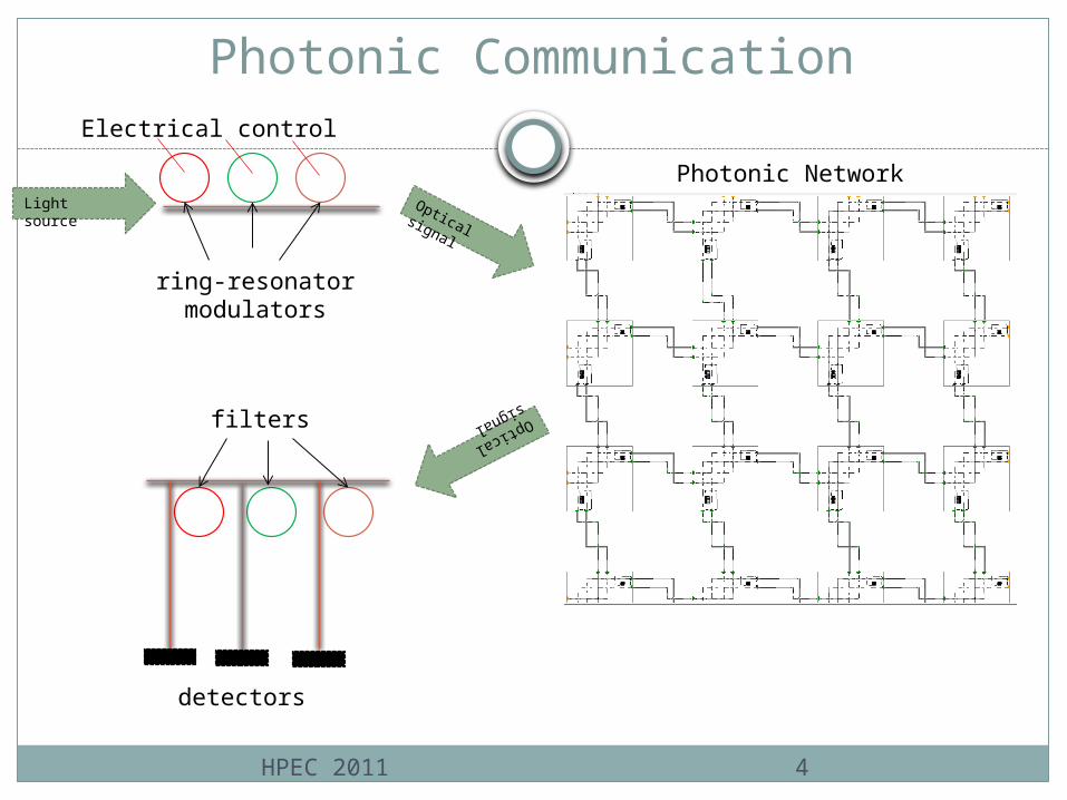
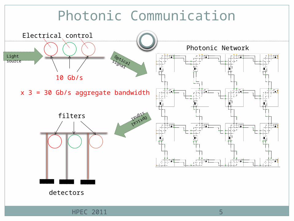
Photonic Communication
Light source Optical signal
Optical signal
ring-resonatormodulators
Electrical control
detectors
filters
Photonic Network
HPEC 2011 4
Photonic Communication
Light source Optical signal
Optical signal
Electrical control
detectors
filters
Photonic Network
10 Gb/s
x 3 = 30 Gb/s aggregate bandwidth
HPEC 2011 5

Optical Power BudgetO
pti
cal P
ow
er
Detector Sensitivity
Nonlinear Effects
Total Injected Power
Received Power
Maximum Network-Level Insertion Loss
Injected Power Per Wavelength
Ptotal = Pchannel × N
1 dBm
1 mm
0.68 dBm
waveguide propagation-1.0 dB/cm
total insertion loss0.32 dB
waveguide crossing-0.05 dB each
passing by a ring -0.01 dB each
The total injectable power Ptotal must remain below a threshold to avoid non-linear effects. Ptotal is then divided among the N wavelengths of a WDM packet, where each channels injects at Pchannel.
HPEC 2011 6

Silicon Photonics Technologies
Crystalline Silicon Best electrical and optical properties
Unable to deposit
Material Propagation Loss
CrystallineSilicon
1.7 dB/cm[Xia et al.
2007]
HPEC 2011 9

Silicon Photonics Technologies
Crystalline Silicon Best electrical and optical properties
Unable to deposit
Polycrystalline Silicon Can deposit
Very lossy
Material Propagation Loss
CrystallineSilicon
1.7 dB/cm[Xia et al.
2007]
Polycrystalline
Silicon
6.45 dB/cm[Fang et al.
2008]
HPEC 2011 9

Silicon Photonics Technologies
Crystalline Silicon Best electrical and optical properties
Unable to deposit
Polycrystalline Silicon Can deposit
Very lossy
Silicon Nitride Very low loss
Can deposit
Not useful active devices
Material Propagation Loss
CrystallineSilicon
1.7 dB/cm[Xia et al.
2007]
Polycrystalline
Silicon
6.45 dB/cm[Fang et al.
2008]
SiliconNitride
0.1 dB/cm[Shaw et al.
2005] [Gondarenko et
al. 2009]
HPEC 2011 9

Poly-Si / SiN Combination approach
We can use silicon nitride and polycrystalline silicon in combination
SiN for non-active wave guides
Poly-Si for active devices (e.g. ring-resonator based switch)
Designs for a layered modulatorand switch
HPEC 2011 10
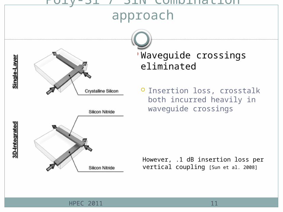
Poly-Si / SiN Combination approach
Waveguide crossings eliminated
Insertion loss, crosstalk both incurred heavily in waveguide crossings
• However, .1 dB insertion loss per vertical coupling [Sun et al. 2008]
HPEC 2011 11

Insertion Loss Analysis
Worst-case insertion loss for a photonic mesh
[Biberman et al. 2011]
HPEC 2011 12

Insertion Loss Analysis
Worst-case insertion loss for a photonic mesh
[Biberman et al. 2011]
HPEC 2011 13

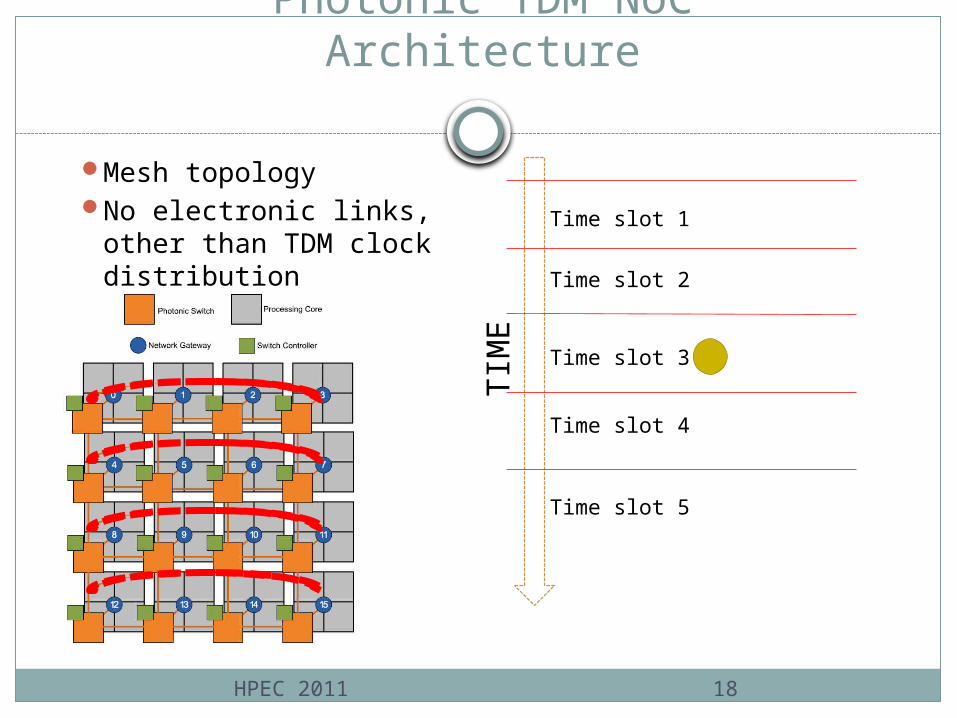
Photonic TDM NoC Architecture
Mesh topologyNo electronic links,
other than TDM clock distribution
TIM
E
Time slot 1
Time slot 2
Time slot 3
Time slot 4
Time slot 5
HPEC 2011 15

Photonic TDM NoC Architecture
Mesh topologyNo electronic links,
other than TDM clock distribution
TIM
E
Time slot 1
Time slot 2
Time slot 3
Time slot 4
Time slot 5
HPEC 2011 16

Photonic TDM NoC Architecture
Mesh topologyNo electronic links,
other than TDM clock distribution
TIM
E
Time slot 1
Time slot 2
Time slot 3
Time slot 4
Time slot 5
HPEC 2011 17
Photonic TDM NoC Architecture
Mesh topologyNo electronic links,
other than TDM clock distribution
TIM
E
Time slot 1
Time slot 2
Time slot 3
Time slot 4
Time slot 5
HPEC 2011 18
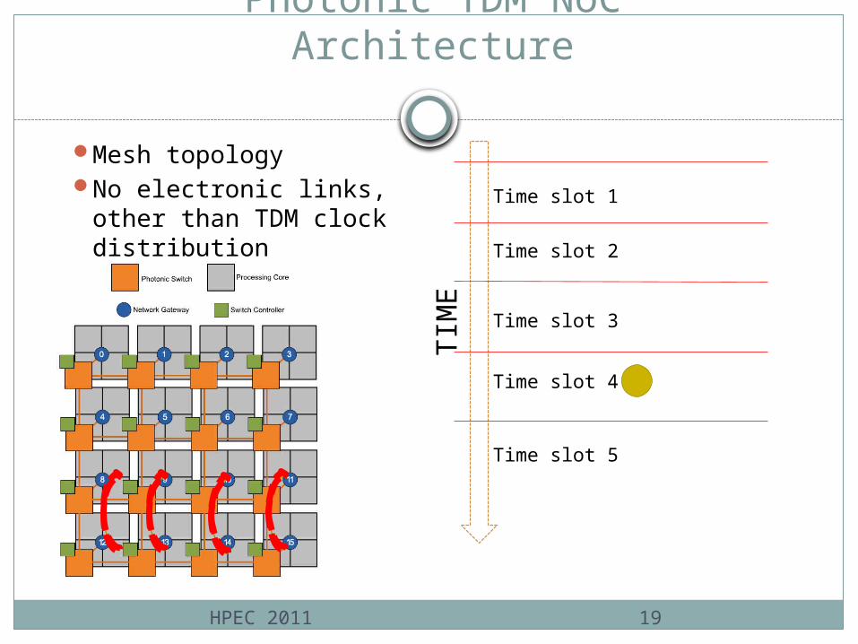
Photonic TDM NoC Architecture
Mesh topologyNo electronic links,
other than TDM clock distribution
TIM
E
Time slot 1
Time slot 2
Time slot 3
Time slot 4
Time slot 5
HPEC 2011 19
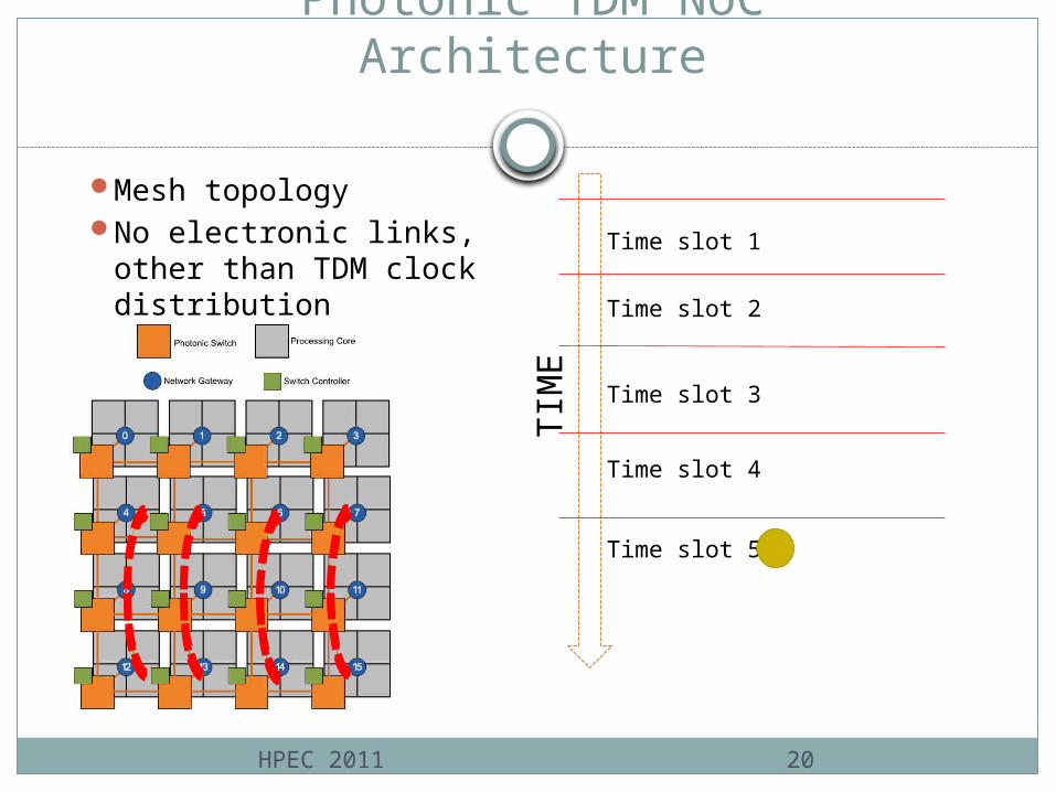
Photonic TDM NoC Architecture
Mesh topologyNo electronic links,
other than TDM clock distribution
TIM
E
Time slot 1
Time slot 2
Time slot 3
Time slot 4
Time slot 5
HPEC 2011 20

X-Y Buffering
Mesh topologyNo electronic links,
other than TDM clock distribution
Op
tica
l Po
wer
Detector Sensitivity
Nonlinear Effects
Maximum Network-Level Insertion Loss
Ptotal = Pchannel × N
HPEC 2011 21

Photonic TDM vs. Photonic Circuit-Switched Insertion Loss
HPEC 2011 22

Single-Layer Switch vs. Multi-layer Switch
Single-layer TDM Switch Multi-layer TDM Switch
Control
East
1
25
6
3
7
4
8
North
South
West
Gateway
HPEC 2011 23

Single-Layer Switch vs. Multi-layer Switch
Single-layer TDM Switch Multi-layer TDM Switch
Control
East
1
25
6
3
7
4
8
North
South
West
Gateway
HPEC 2011 23
18 crossings 4 crossings
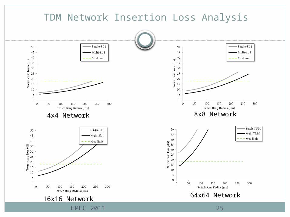
TDM Network Insertion Loss Analysis
4x4 Network 8x8 Network
16x16 Network64x64 Network
HPEC 2011 25

Maximum Bandwidth (# of Wavelengths)
4x4 Network 8x8 Network
16x16 Network 64x64 Network
HPEC 2011 26
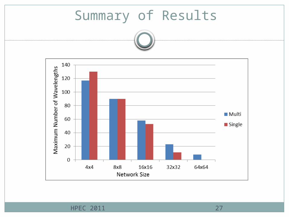
Summary of Results
HPEC 2011 27

Conclusions
Poly-Silicon and Silicon Nitride in conjunction are a good choice of materials for photonic interconnection networks Low-loss = more wavelengths = higher bandwidth
We’ve shown that our best network, when at large scale, can be improved with a multi-layer implementation
Future work: We expect the elimination of waveguide crossings to significantly reduce crosstalk across a wide variety of network architectures
HPEC 2011 28