Embed Size (px)
Citation preview

Sales Information Phone:(425) 353-3010 Fax: (425) 353-4030 SVRFL2800D - 8.0
E-mail: [email protected] Web: www.vptpower.com Page 1
SVRFL2800D SERIES
SPACE QUALIFIED HYBRID DC-DC CONVERTERS
SVRFL Series DC-DC Converter
Models Available
Input: 18 V to 40 V continuous, 50 V transient
100 W, dual outputs of ±5 V, ±12 V, ±15 V
Qualified to MIL-PRF-38534 Class H and Class K
Designed for TOR Compliance
1.0 DESCRIPTION
The SVRFL Series of space qualified DC-DC converters is
specifically designed for the harsh radiation environment of
space applications and is designed in accordance with
Aerospace TOR requirements. Performance is guaranteed
through the use of hardened semiconductor components,
radiation lot acceptance testing (RLAT) of non-hardened
components, and analysis. The SVRFL Series has been
characterized for Total Ionizing Dose (TID) performance
including Enhanced Low Dose Rate Sensitivity (ELDRS) and for
Single Event Effects (SEE) according to VPT’s DLA-approved
Radiation Hardness Assurance (RHA) plan per MIL-PRF-38534,
Appendix G, Level R. Characterization is performed at both the
component level and at the SVRFL Series hybrid converter level.
The SVRFL Series of DC-DC converters is radiation hardened
and suited for use in low Earth orbit (LEO), medium Earth orbit
(MEO), geostationary orbit (GEO), deep space, and launch
vehicle programs.
1.1 FEATURES
• Up to 100 W output power
• Wide input voltage range: 18 V to 40 V plus 50 V transient
• Continuous operation over full military temperature range of
-55 °C to +125 °C with no power derating
• Very low output noise
• Parallel up to 5 units with current sharing
• Output voltage trim up +10% or down -20%
• Radiation immune magnetic feedback circuit
• No use of optoisolators
• Undervoltage lockout
• Current limit protection / short circuit protection
1.2 SPACE LEVEL CHARACTERIZATIONS
• Guaranteed TID performance to 100 krad(Si) including ELDRS
• SEE performance to 85 MeV-cm2/mg. Transients are fully
characterized for cross section and magnitude
• Worst-case analysis, stress, radiation, reliability reports available
1.3 MANUFACTURING AND COMPLIANCE
• Qualified to MIL-PRF-38534 Class H and Class K,
DLA SMD # 5962-13234
• Available compliant to MIL-HDBK-1547 and Aerospace TOR
component level element evaluation
• MIL-PRF-38534 element evaluated components
• MIL-STD-461 C/D/E/F when used with appropriate VPT EMI filter
• Manufactured in a MIL-PRF-38534 Class H and Class K facility
• MIL-STD-883
• ISO-9001
1.4 PACKAGING
• Low-profile: 3.005” x 1.505” x 0.400”
• Max weight: 88 g
• Industry standard pinout
• Precision seam-welded hermetic metal case
1.5 SIMILAR PRODUCTS AND ACCESSORIES
• SVRFL 100 W single output DC-DC converter
• SVFL 100 W space qualified DC-DC converter, 30 krad(Si)
• Custom versions available
• EMI filters
• Non-isolated, space qualified point of load converters
• Use with Thermal Pad TP-001
Products and reports described in this datasheet are subject to all export license restrictions and regulations which may inc lude but are not limited to ITAR (International Traffic in Arms Regulations) and the Export Administration and Foreign Assets Control Regulations. Further restrictions may apply. Contact VPT sales for details.
Sales Information Phone:(425) 353-3010 Fax: (425) 353-4030 SVRFL2800D - 8.0
E-mail: [email protected] Web: www.vptpower.com Page 2
SVRFL2800D Series
2.0 DIAGRAMS
2.1 BLOCK DIAGRAM
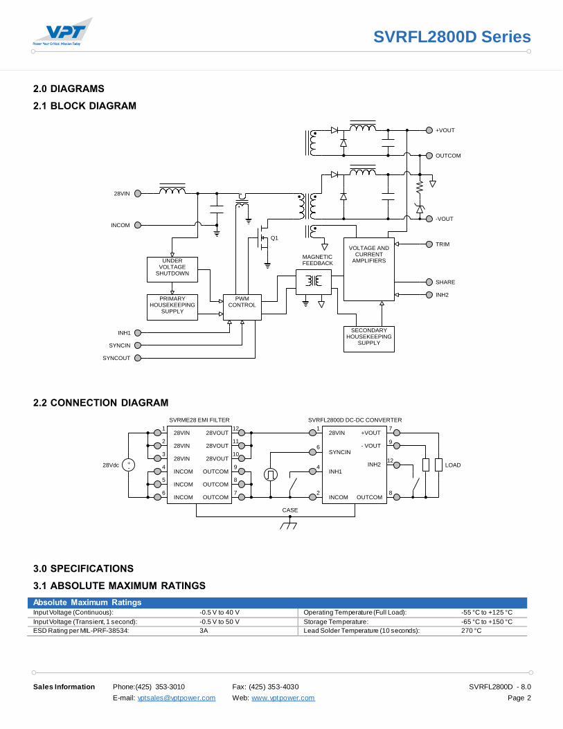
2.2 CONNECTION DIAGRAM
3.0 SPECIFICATIONS
3.1 ABSOLUTE MAXIMUM RATINGS
Absolute Maximum Ratings Input Voltage (Continuous): -0.5 V to 40 V Operating Temperature (Full Load): -55 °C to +125 °C
Input Voltage (Transient, 1 second): -0.5 V to 50 V Storage Temperature: -65 °C to +150 °C
ESD Rating per MIL-PRF-38534: 3A Lead Solder Temperature (10 seconds): 270 °C
UNDERVOLTAGE
SHUTDOWN
PRIMARYHOUSEKEEPING
SUPPLY
PWMCONTROL
VOLTAGE ANDCURRENT
AMPLIFIERS
SECONDARYHOUSEKEEPING
SUPPLY
28VIN
INCOM
Q1
+VOUT
OUTCOM
INH1
FEEDBACKMAGNETIC
SYNCIN
SYNCOUT
TRIM
SHARE
INH2
-VOUT
2INCOM
4INH1
128VIN
7+VOUT
8OUTCOM
LOAD+-28Vdc
1228VOUT
7OUTCOM
128VIN
6INCOM
CASE
- VOUT9
INH212
SYNCIN628VIN
2
28VIN3
INCOM4
INCOM5
28VOUT11
28VOUT10
OUTCOM9
OUTCOM8
SVRME28 EMI FILTER SVRFL2800D DC-DC CONVERTER
Sales Information Phone:(425) 353-3010 Fax: (425) 353-4030 SVRFL2800D - 8.0
E-mail: [email protected] Web: www.vptpower.com Page 3
SVRFL2800D Series
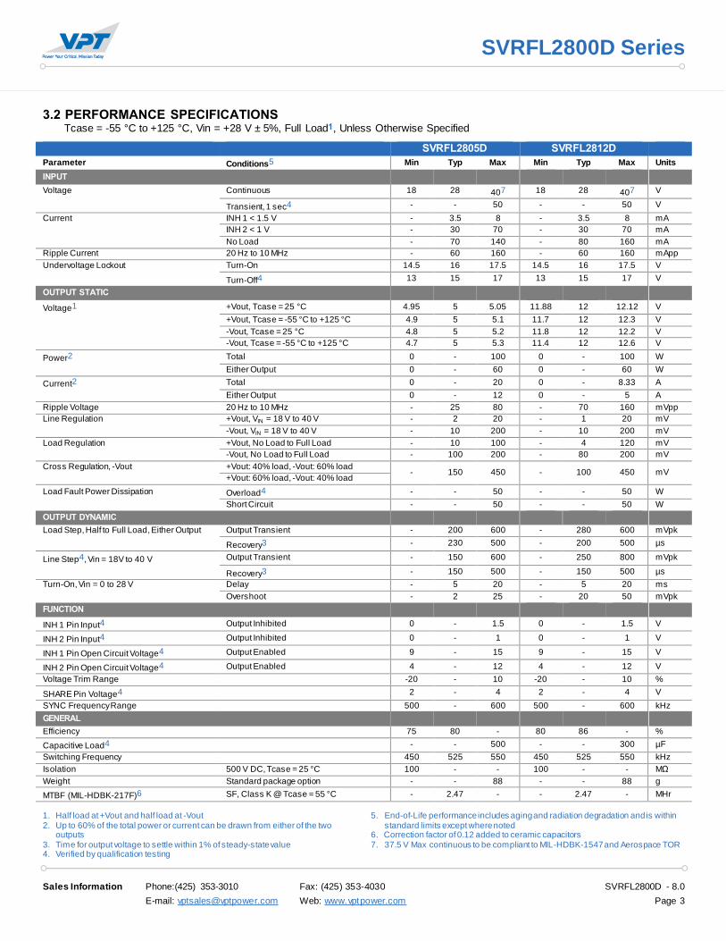
3.2 PERFORMANCE SPECIFICATIONS
Tcase = -55 °C to +125 °C, Vin = +28 V ± 5%, Full Load1, Unless Otherwise Specified
SVRFL2805D SVRFL2812D Parameter Conditions5 Min Typ Max Min Typ Max Units
INPUT
Voltage Continuous 18 28 407 18 28 407 V
Transient, 1 sec4 - - 50 - - 50 V
Current INH 1 < 1.5 V - 3.5 8 - 3.5 8 mA
INH 2 < 1 V - 30 70 - 30 70 mA
No Load - 70 140 - 80 160 mA
Ripple Current 20 Hz to 10 MHz - 60 160 - 60 160 mApp
Undervoltage Lockout Turn-On 14.5 16 17.5 14.5 16 17.5 V
Turn-Off4 13 15 17 13 15 17 V
OUTPUT STATIC
Voltage1 +Vout, Tcase = 25 °C 4.95 5 5.05 11.88 12 12.12 V
+Vout, Tcase = -55 °C to +125 °C 4.9 5 5.1 11.7 12 12.3 V
-Vout, Tcase = 25 °C 4.8 5 5.2 11.8 12 12.2 V
-Vout, Tcase = -55 °C to +125 °C 4.7 5 5.3 11.4 12 12.6 V
Power2 Total 0 - 100 0 - 100 W
Either Output 0 - 60 0 - 60 W
Current2 Total 0 - 20 0 - 8.33 A
Either Output 0 - 12 0 - 5 A
Ripple Voltage 20 Hz to 10 MHz - 25 80 - 70 160 mVpp
Line Regulation +Vout, VIN = 18 V to 40 V - 2 20 - 1 20 mV
-Vout, VIN = 18 V to 40 V - 10 200 - 10 200 mV
Load Regulation +Vout, No Load to Full Load - 10 100 - 4 120 mV
-Vout, No Load to Full Load - 100 200 - 80 200 mV
Cross Regulation, -Vout +Vout: 40% load, -Vout: 60% load - 150 450 - 100 450 mV
+Vout: 60% load, -Vout: 40% load
Load Fault Power Dissipation Overload4 - - 50 - - 50 W
Short Circuit - - 50 - - 50 W
OUTPUT DYNAMIC
Load Step, Half to Full Load, Either Output Output Transient - 200 600 - 280 600 mVpk
Recovery3 - 230 500 - 200 500 µs
Line Step4, Vin = 18V to 40 V Output Transient - 150 600 - 250 800 mVpk
Recovery3 - 150 500 - 150 500 µs
Turn-On, Vin = 0 to 28 V Delay - 5 20 - 5 20 ms
Overshoot - 2 25 - 20 50 mVpk
FUNCTION
INH 1 Pin Input4 Output Inhibited 0 - 1.5 0 - 1.5 V
INH 2 Pin Input4 Output Inhibited 0 - 1 0 - 1 V
INH 1 Pin Open Circuit Voltage4 Output Enabled 9 - 15 9 - 15 V
INH 2 Pin Open Circuit Voltage4 Output Enabled 4 - 12 4 - 12 V
Voltage Trim Range -20 - 10 -20 - 10 %
SHARE Pin Voltage4 2 - 4 2 - 4 V
SYNC Frequency Range 500 - 600 500 - 600 kHz
GENERAL
Efficiency 75 80 - 80 86 - %
Capacitive Load4 - - 500 - - 300 µF
Switching Frequency 450 525 550 450 525 550 kHz
Isolation 500 V DC, Tcase = 25 °C 100 - - 100 - - MΩ
Weight Standard package option - - 88 - - 88 g
MTBF (MIL-HDBK-217F)6 SF, Class K @ Tcase = 55 °C - 2.47 - - 2.47 - MHr
1. Half load at +Vout and half load at -Vout 2. Up to 60% of the total power or current can be drawn from either of the two
outputs 3. Time for output voltage to settle within 1% of steady-state value 4. Verified by qualification testing
5. End-of-Life performance includes aging and radiation degradation and is within standard limits except where noted 6. Correction factor of 0.12 added to ceramic capacitors 7. 37.5 V Max continuous to be compliant to MIL-HDBK-1547 and Aerospace TOR
Sales Information Phone:(425) 353-3010 Fax: (425) 353-4030 SVRFL2800D - 8.0
E-mail: [email protected] Web: www.vptpower.com Page 4
SVRFL2800D Series
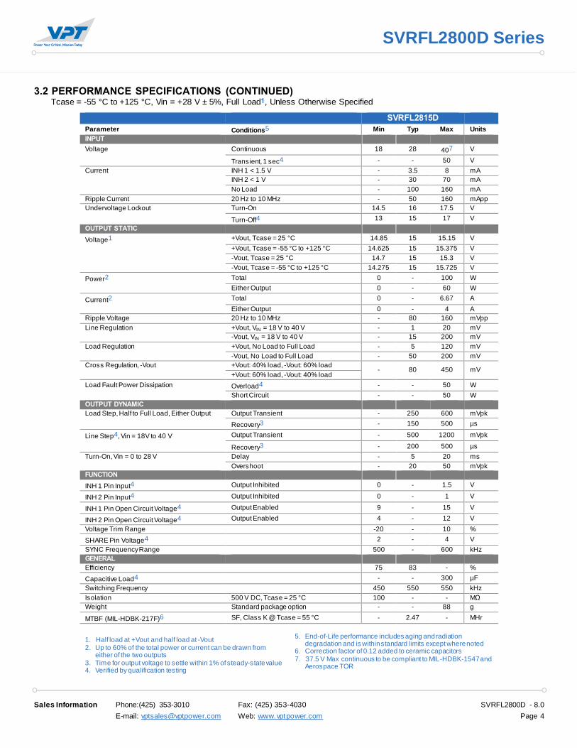
3.2 PERFORMANCE SPECIFICATIONS (CONTINUED)
Tcase = -55 °C to +125 °C, Vin = +28 V ± 5%, Full Load1, Unless Otherwise Specified
SVRFL2815D Parameter Conditions5 Min Typ Max Units
INPUT
Voltage Continuous 18 28 407 V
Transient, 1 sec4 - - 50 V
Current INH 1 < 1.5 V - 3.5 8 mA
INH 2 < 1 V - 30 70 mA
No Load - 100 160 mA
Ripple Current 20 Hz to 10 MHz - 50 160 mApp
Undervoltage Lockout Turn-On 14.5 16 17.5 V
Turn-Off4 13 15 17 V
OUTPUT STATIC
Voltage1 +Vout, Tcase = 25 °C 14.85 15 15.15 V
+Vout, Tcase = -55 °C to +125 °C 14.625 15 15.375 V
-Vout, Tcase = 25 °C 14.7 15 15.3 V
-Vout, Tcase = -55 °C to +125 °C 14.275 15 15.725 V
Power2 Total 0 - 100 W
Either Output 0 - 60 W
Current2 Total 0 - 6.67 A
Either Output 0 - 4 A
Ripple Voltage 20 Hz to 10 MHz - 80 160 mVpp
Line Regulation +Vout, VIN = 18 V to 40 V - 1 20 mV
-Vout, VIN = 18 V to 40 V - 15 200 mV
Load Regulation +Vout, No Load to Full Load - 5 120 mV
-Vout, No Load to Full Load - 50 200 mV
Cross Regulation, -Vout +Vout: 40% load, -Vout: 60% load - 80 450 mV
+Vout: 60% load, -Vout: 40% load
Load Fault Power Dissipation Overload4 - - 50 W
Short Circuit - - 50 W
OUTPUT DYNAMIC
Load Step, Half to Full Load, Either Output Output Transient - 250 600 mVpk
Recovery3 - 150 500 µs
Line Step4, Vin = 18V to 40 V Output Transient - 500 1200 mVpk
Recovery3 - 200 500 µs
Turn-On, Vin = 0 to 28 V Delay - 5 20 ms
Overshoot - 20 50 mVpk
FUNCTION
INH 1 Pin Input4 Output Inhibited 0 - 1.5 V
INH 2 Pin Input4 Output Inhibited 0 - 1 V
INH 1 Pin Open Circuit Voltage4 Output Enabled 9 - 15 V
INH 2 Pin Open Circuit Voltage4 Output Enabled 4 - 12 V
Voltage Trim Range -20 - 10 %
SHARE Pin Voltage4 2 - 4 V
SYNC Frequency Range 500 - 600 kHz
GENERAL
Efficiency 75 83 - %
Capacitive Load4 - - 300 µF
Switching Frequency 450 550 550 kHz
Isolation 500 V DC, Tcase = 25 °C 100 - - MΩ
Weight Standard package option - - 88 g
MTBF (MIL-HDBK-217F)6 SF, Class K @ Tcase = 55 °C - 2.47 - MHr
1. Half load at +Vout and half load at -Vout 2. Up to 60% of the total power or current can be drawn from
either of the two outputs 3. Time for output voltage to settle within 1% of steady-state value 4. Verified by qualification testing
5. End-of-Life performance includes aging and radiation degradation and is within standard limits except where noted
6. Correction factor of 0.12 added to ceramic capacitors 7. 37.5 V Max continuous to be compliant to MIL-HDBK-1547 and
Aerospace TOR
Sales Information Phone:(425) 353-3010 Fax: (425) 353-4030 SVRFL2800D - 8.0
E-mail: [email protected] Web: www.vptpower.com Page 5
SVRFL2800D Series
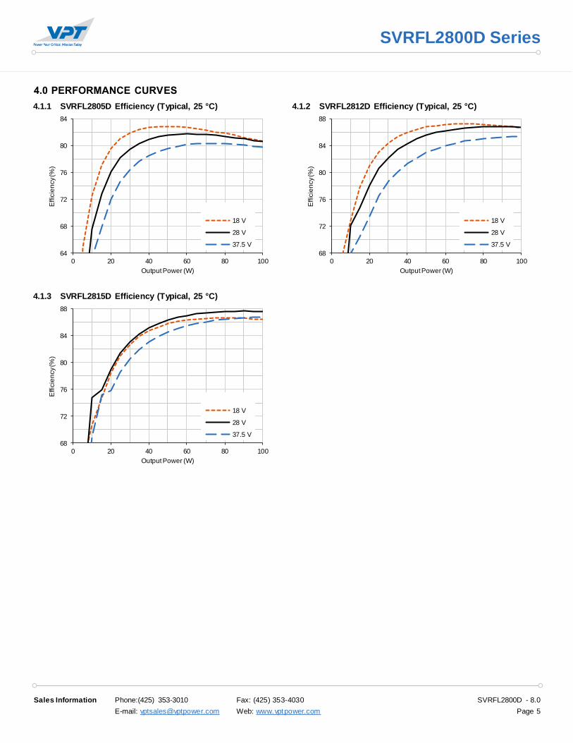
4.0 PERFORMANCE CURVES
4.1.1 SVRFL2805D Efficiency (Typical, 25 °C) 4.1.2 SVRFL2812D Efficiency (Typical, 25 °C)
4.1.3 SVRFL2815D Efficiency (Typical, 25 °C)
64
68
72
76
80
84
0 20 40 60 80 100
Effic
ien
cy
(%)
Output Power (W)
18 V
28 V
37.5 V
68
72
76
80
84
88
0 20 40 60 80 100
Effic
ien
cy
(%)
Output Power (W)
18 V
28 V
37.5 V
68
72
76
80
84
88
0 20 40 60 80 100
Effic
ien
cy
(%)
Output Power (W)
18 V
28 V
37.5 V
Sales Information Phone:(425) 353-3010 Fax: (425) 353-4030 SVRFL2800D - 8.0
E-mail: [email protected] Web: www.vptpower.com Page 6
SVRFL2800D Series
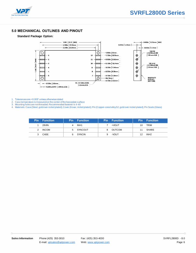
5.0 MECHANICAL OUTLINES AND PINOUT
Standard Package Option:
1. Tolerances are +0.005” unless otherwise stated 2. Case temperature is measured on the center of the baseplate surface 3. Mounting holes are not threaded. Recommended fastener is 4-40 4. Materials: Case (Steel, gold over nickel plated); Cover (Kovar, nickel plated); Pin (Copper-cored alloy 52, gold over nickel plated); Pin Seals (Glass)
Pin Function Pin Function Pin Function Pin Function
1 28VIN 4 INH1 7 +VOUT 10 TRIM
2 INCOM 5 SYNCOUT 8 OUTCOM 11 SHARE
3 CASE 6 SYNCIN 9 -VOUT 12 INH2
Sales Information Phone:(425) 353-3010 Fax: (425) 353-4030 SVRFL2800D - 8.0
E-mail: [email protected] Web: www.vptpower.com Page 7
SVRFL2800D Series
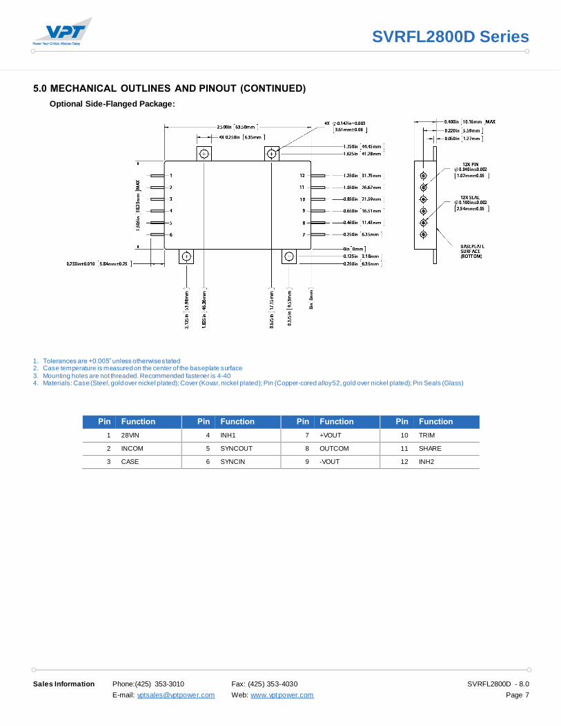
5.0 MECHANICAL OUTLINES AND PINOUT (CONTINUED)
Optional Side-Flanged Package:
1. Tolerances are +0.005” unless otherwise stated 2. Case temperature is measured on the center of the baseplate surface 3. Mounting holes are not threaded. Recommended fastener is 4-40 4. Materials: Case (Steel, gold over nickel plated); Cover (Kovar, nickel plated); Pin (Copper-cored alloy 52, gold over nickel plated); Pin Seals (Glass)
Pin Function Pin Function Pin Function Pin Function
1 28VIN 4 INH1 7 +VOUT 10 TRIM
2 INCOM 5 SYNCOUT 8 OUTCOM 11 SHARE
3 CASE 6 SYNCIN 9 -VOUT 12 INH2
Sales Information Phone:(425) 353-3010 Fax: (425) 353-4030 SVRFL2800D - 8.0
E-mail: [email protected] Web: www.vptpower.com Page 8
SVRFL2800D Series
6.0 TECHNICAL NOTES
Please note that many of these functions are also demonstrated in detail on the VPT website in the
form of technical video labs.
6.1 GENERAL INFORMATION
6.1.1 Topology Description
The SVRFL2800D Series is an isolated dual-output flyback converter. It provides a positive and negative output voltage with respect to
the OUTCOM pin. Up to 60% of the total output power is available from either output. The internal voltage regulation loop actively
regulates the positive output using VPT’s proprietary magnetic feedback technology. The negative output is regulated by cross-
regulation of the transformer windings. The negative output is well-regulated for balanced load conditions. For unbalanced load
conditions, refer to the cross regulation performance graphs in Section 4.2 for expected performance. For a balanced or near-balanced
load condition, the converter will regulate down to zero load, and no minimum load is required. For an unbalanced load condit ion, with
negative loads greater than 10%, a minimum load of 10% is recommended on the positive output.
6.1.2 External Components
The SVRFL2800D Series is designed to operate stand-alone in most applications. It does not require any external components for
proper operation or to meet the datasheet specifications. Input and output L-C filters are provided internally for low ripple and noise. To
further reduce output ripple and noise, a small ceramic capacitor, 1 µF to 10 µF, can be added at the output. Most application specific
ripple requirements can be met with the addition of output capacitors alone. External output capacitance can be added up to the
maximum listed in Section 3.2.
6.1.3 Source Impedance
The impedance of the 28 V input source can interact with the DC-DC converter and can affect performance. High source impedance is
often caused by a long input cable or components added in series with the input. Source resistance will cause a DC voltage drop as the
converter draws DC input current. This voltage drop is simply the cable resistance multiplied by the input current at low line. The
voltage drop and the actual voltage at the input to the converter will determine the minimum source voltage at which the converter will
operate. A high source inductance can interact with the feedback control loop of the converter. VPT’s EMI filters will usually isolate the
source and eliminate this problem. In some cases, additional input capacitance will be needed to stabilize the system.
6.1.4 Output Configurations
Since the converter is isolated, the outputs can be used as a traditional dual-output, with a positive and negative voltage referenced to
OUTCOM, or as a single-ended output referenced to –VOUT or +VOUT. For example, the SVRFL2812D model can provide +12 V and
-12 V in the traditional dual output configuration, or can provide +24 V referenced to –VOUT, or -24 V referenced to +VOUT in single-
ended configuration. In the single-ended configuration, the OUTCOM pin will be at +12 V relative to –VOUT.
The outputs of multiple converters can be stacked in series to provide higher voltages. When outputs of multiple modules are stacked,
they naturally share the load. For example, two SVRFL2812D converters can be stacked to provide a 48 V output at 200 W.
6.2 FUNCTION DESCRIPTIONS
6.2.1 On/Off Control (INH1 and INH2)
The INH1 (Inhibit 1) pin is a primary-side control pin referenced to IN COM.
The INH1 pin must be driven using an open collector or open drain
configuration. Pulling the INH1 pin low disables the converter output,
removes bias voltage from internal control circuitry, and puts the converter
in a state of minimum input current draw. Leaving INH1 open enables the
output, allowing the converter to operate normally. The pin must be pulled
below 1.5 V to disable the output. An optional capacitor from INH1 to
INCOM may be used to delay turn-on. The INH1 pin should be left open if
not used.
Sales Information Phone:(425) 353-3010 Fax: (425) 353-4030 SVRFL2800D - 8.0
E-mail: [email protected] Web: www.vptpower.com Page 9
SVRFL2800D Series
The INH2 (Inhibit 2) pin is a secondary-side control pin referenced to OUTCOM. The INH2 pin must also be driven in an open collector
or open drain configuration. Pulling INH2 low to OUTCOM disables the converter output. Internal control circuits, however, remain
active. The pin must be pulled below 1.0 V to disable the output. The INH2 pin should be left open if not used.
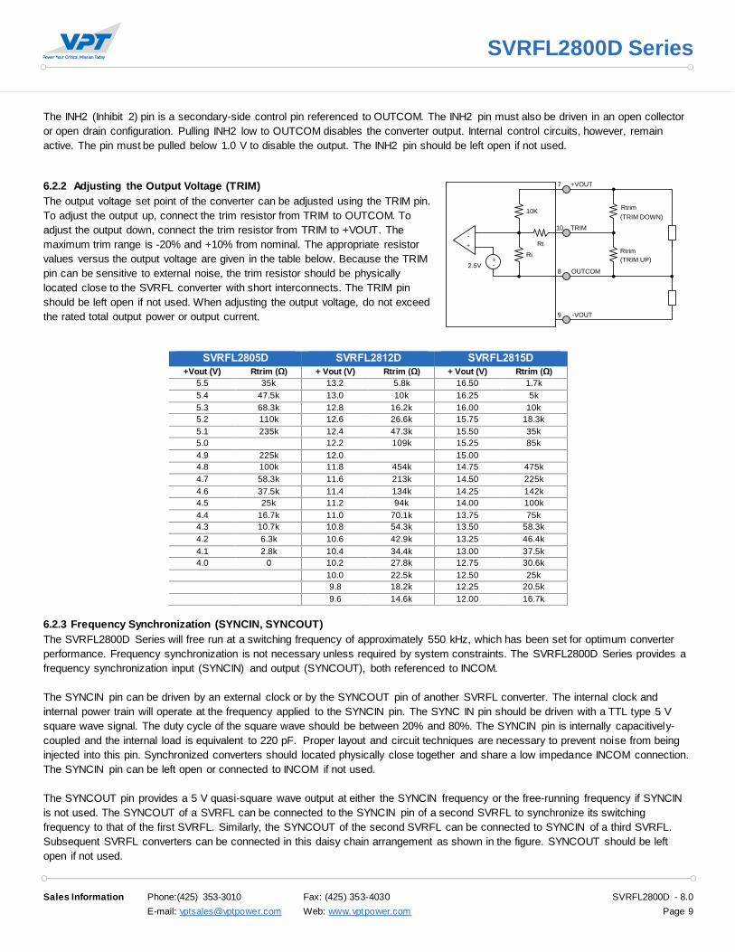
6.2.2 Adjusting the Output Voltage (TRIM)
The output voltage set point of the converter can be adjusted using the TRIM pin.
To adjust the output up, connect the trim resistor from TRIM to OUTCOM. To
adjust the output down, connect the trim resistor from TRIM to +VOUT. The
maximum trim range is -20% and +10% from nominal. The appropriate resistor
values versus the output voltage are given in the table below. Because the TRIM
pin can be sensitive to external noise, the trim resistor should be physically
located close to the SVRFL converter with short interconnects. The TRIM pin
should be left open if not used. When adjusting the output voltage, do not exceed
the rated total output power or output current.
SVRFL2805D SVRFL2812D SVRFL2815D
+Vout (V) Rtrim (Ω) + Vout (V) Rtrim (Ω) + Vout (V) Rtrim (Ω)
5.5 35k 13.2 5.8k 16.50 1.7k
5.4 47.5k 13.0 10k 16.25 5k
5.3 68.3k 12.8 16.2k 16.00 10k
5.2 110k 12.6 26.6k 15.75 18.3k
5.1 235k 12.4 47.3k 15.50 35k
5.0 12.2 109k 15.25 85k
4.9 225k 12.0 15.00
4.8 100k 11.8 454k 14.75 475k
4.7 58.3k 11.6 213k 14.50 225k
4.6 37.5k 11.4 134k 14.25 142k
4.5 25k 11.2 94k 14.00 100k
4.4 16.7k 11.0 70.1k 13.75 75k
4.3 10.7k 10.8 54.3k 13.50 58.3k
4.2 6.3k 10.6 42.9k 13.25 46.4k
4.1 2.8k 10.4 34.4k 13.00 37.5k
4.0 0 10.2 27.8k 12.75 30.6k
10.0 22.5k 12.50 25k
9.8 18.2k 12.25 20.5k
9.6 14.6k 12.00 16.7k
6.2.3 Frequency Synchronization (SYNCIN, SYNCOUT)
The SVRFL2800D Series will free run at a switching frequency of approximately 550 kHz, which has been set for optimum converter
performance. Frequency synchronization is not necessary unless required by system constraints. The SVRFL2800D Series provides a
frequency synchronization input (SYNCIN) and output (SYNCOUT), both referenced to INCOM.
The SYNCIN pin can be driven by an external clock or by the SYNCOUT pin of another SVRFL converter. The internal clock and
internal power train will operate at the frequency applied to the SYNCIN pin. The SYNC IN pin should be driven with a TTL type 5 V
square wave signal. The duty cycle of the square wave should be between 20% and 80%. The SYNCIN pin is internally capacitively-
coupled and the internal load is equivalent to 220 pF. Proper layout and circuit techniques are necessary to prevent noise from being
injected into this pin. Synchronized converters should located physically close together and share a low impedance INCOM connection.
The SYNCIN pin can be left open or connected to INCOM if not used.
The SYNCOUT pin provides a 5 V quasi-square wave output at either the SYNCIN frequency or the free-running frequency if SYNCIN
is not used. The SYNCOUT of a SVRFL can be connected to the SYNCIN pin of a second SVRFL to synchronize its switching
frequency to that of the first SVRFL. Similarly, the SYNCOUT of the second SVRFL can be connected to SYNCIN of a third SVRFL.
Subsequent SVRFL converters can be connected in this daisy chain arrangement as shown in the figure. SYNCOUT should be left
open if not used.
+
-
+-2.5V
Ri
10K
Rt
TRIM10
(TRIM DOWN)
Rtrim
(TRIM UP)
Rtrim
+VOUT7
OUTCOM8
-VOUT9
Sales Information Phone:(425) 353-3010 Fax: (425) 353-4030 SVRFL2800D - 8.0
E-mail: [email protected] Web: www.vptpower.com Page 10
SVRFL2800D Series
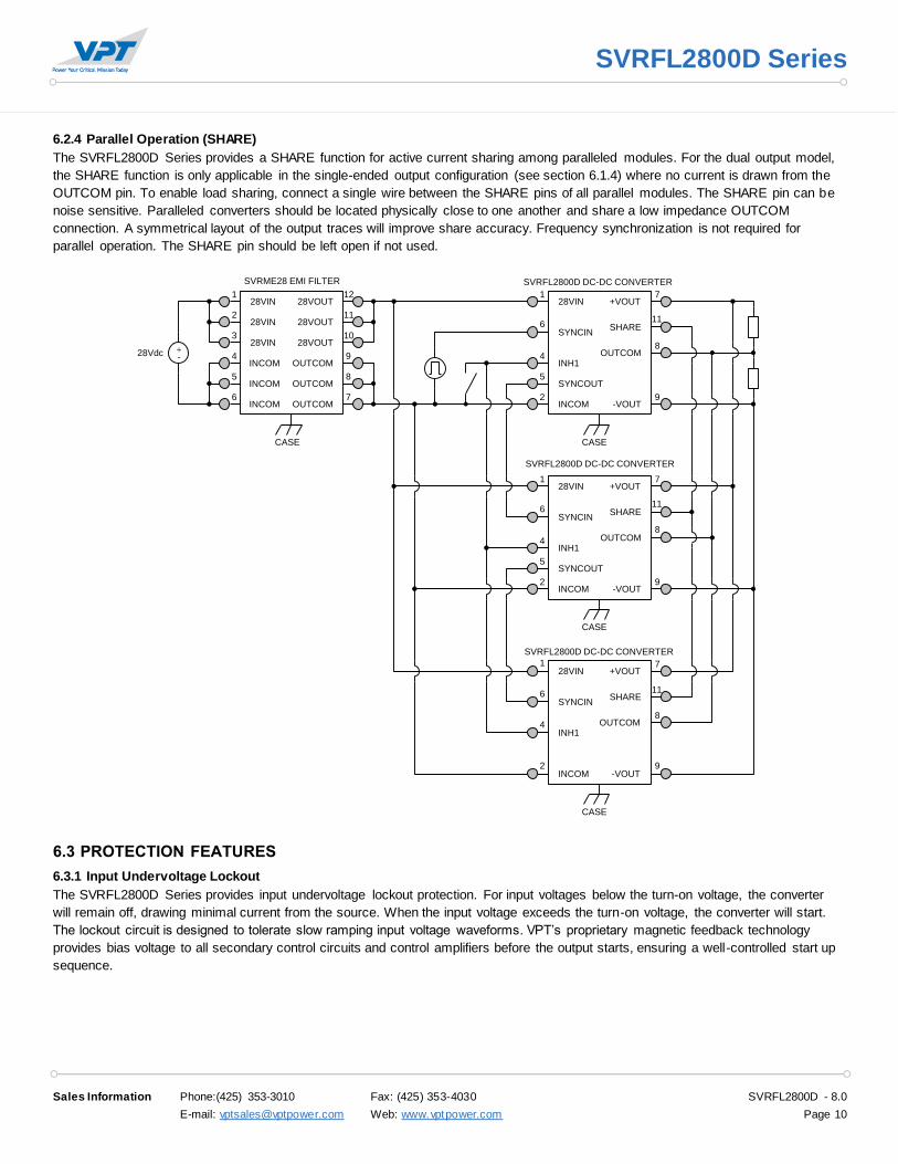
6.2.4 Parallel Operation (SHARE)
The SVRFL2800D Series provides a SHARE function for active current sharing among paralleled modules. For the dual output model,
the SHARE function is only applicable in the single-ended output configuration (see section 6.1.4) where no current is drawn from the
OUTCOM pin. To enable load sharing, connect a single wire between the SHARE pins of all parallel modules. The SHARE pin can be
noise sensitive. Paralleled converters should be located physically close to one another and share a low impedance OUTCOM
connection. A symmetrical layout of the output traces will improve share accuracy. Frequency synchronization is not required for
parallel operation. The SHARE pin should be left open if not used.
6.3 PROTECTION FEATURES
6.3.1 Input Undervoltage Lockout
The SVRFL2800D Series provides input undervoltage lockout protection. For input voltages below the turn-on voltage, the converter
will remain off, drawing minimal current from the source. When the input voltage exceeds the turn-on voltage, the converter will start.
The lockout circuit is designed to tolerate slow ramping input voltage waveforms. VPT’s proprietary magnetic feedback technology
provides bias voltage to all secondary control circuits and control amplifiers before the output starts, ensuring a well-controlled start up
sequence.
2INCOM
4INH1
128VIN
7+VOUT
8OUTCOM+
-28Vdc
1228VOUT
7OUTCOM
128VIN
6INCOM
CASE
-VOUT9
SYNCIN628VIN
2
28VIN3
INCOM4
INCOM5
28VOUT11
28VOUT10
OUTCOM9
OUTCOM8
SVRME28 EMI FILTER SVRFL2800D DC-DC CONVERTER
CASE
5SYNCOUT
11SHARE
2INCOM
4INH1
128VIN
7+VOUT
8OUTCOM
-VOUT9
SYNCIN6
SVRFL2800D DC-DC CONVERTER
CASE
5SYNCOUT
11SHARE
2INCOM
4INH1
128VIN
7+VOUT
8OUTCOM
-VOUT9
SYNCIN6
SVRFL2800D DC-DC CONVERTER
CASE
11SHARE
Sales Information Phone:(425) 353-3010 Fax: (425) 353-4030 SVRFL2800D - 8.0
E-mail: [email protected] Web: www.vptpower.com Page 11
SVRFL2800D Series
6.3.2 Output Soft Start
The SVRFL2800D Series utilizes an output soft-start function to ramp the output in a controlled manner, eliminating output voltage
overshoot and limiting inrush current at turn on. A voltage-mode soft-start ensures the output waveform remains consistent regardless
of changes in the load current. The output rise time is approximately 4 ms. The soft-start function is active whether the module is turned
on with an application of input voltage or from release of the inhibit pin. Under normal conditions, current drawn from the source during
turn on will not exceed the full load input current. The turn-on delay time is specified from the application of input voltage (or release of
the inhibit pin) until the output reaches 90% of its final value.
6.3.3 Output Overcurrent Protection
The SVRFL2800D Series provides output overcurrent and output short circuit protection. During a load fault condition, a constant output
current control circuit reduces the converter duty cycle to limit the total output current to approximately 125% its rated value. The
current limit protection circuit limits the sum of output currents in both +Vout and -Vout. It does not distinguish if the current is on the
positive or negative output. The converter will continue to provide constant current into any overload or short circuit condition. This
feature allows the converter to start into any capacitive load. Recovery is automatic and immediate upon removal of the fault condition.
Sustained short circuit or overload operation can cause excessive power dissipation. Care should be taken to control the operating
temperature of the converter in this condition.
6.4 THERMAL CONSIDERATIONS
The SVRFL2800D Series is rated for full power operation at 125 °C. Operation above 125 °C is allowed at reduced power. Specifically,
the output power should be derated linearly from full power at 125 °C to half power at 130 °C and to zero power at 135 °C. The
operating temperature of the converter is specified on the baseplate of the converter. The converter is designed to be conduction-
cooled, with the baseplate mounted to a heat sink, chassis, PCB or other thermal surface. The internal power dissipating components
are mounted to the baseplate of the converter and all heat flow is through the baseplate and mounting flanges. The lid of the converter
does not provide a good thermal path.
The hybrid DC-DC converter contains many semiconductor components. The maximum temperature rise from junction to case is
20 °C at full load.
Sales Information Phone:(425) 353-3010 Fax: (425) 353-4030 SVRFL2800D - 8.0
E-mail: [email protected] Web: www.vptpower.com Page 12
SVRFL2800D Series
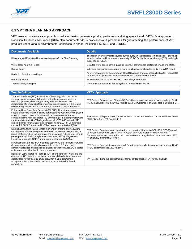
6.5 VPT RHA PLAN AND APPROACH
VPT takes a conservative approach to radiation testing to ensure product performance during space travel. VPT’s DLA approved
Radiation Hardness Assurance (RHA) plan documents VPT’s processes and procedures for guaranteeing the performance of VPT
products under various environmental conditions in space, including TID, SEE, and ELDRS.
Documents Available Details
DLA approved Radiation Hardness Assurance (RHA) Plan Summary The radiation environments covered by this overview include: total ionizing dose (TID), which includes enhanced low dose rate sensitivity (ELDRS); displacement damage (DD); and single event effects (SEE).
Worst-Case Analysis Report Detailed worst-case analysis guarantees circuit performance post radiation and end of life.
Stress Report Individual component stress analysis and deratings are included as part of the WCA report.
Radiation Test Summary Report An overview report on the component level RLAT and characterization testing for TID and DD as well as the hybrid level characterizations for TID and SEE response.
Reliability Report MTBF report based on MIL-HDBK-217 reliability calculations.
Thermal Analysis Report Component temperature rise analysis and measurement results.
Test Definition VPT’s Approach
Total Ionizing Dose (TID). A measure of the energy absorbed in the semiconductor components from the naturally occurring sources of radiation (protons, electrons, photons). This results in the slow degradation of semiconductor performance specifications. TID is tested by exposing components to gamma radiation from a Cobalt-60 source.
SVR Series: Designed for 100 krad(Si). Sensitive semiconductor components undergo RLAT to 100 krad(Si) per MIL-STD-883 Method 1019. Converters are characterized to 100 krad(Si).
Enhanced Low Dose Rate Sensitivity (ELDRS): Many linear-bipolar integrated circuits show enhanced parameter degradation when exposed at low dose rates close to those seen in a space environment as compared to the high dose rates (50-300 rad(Si)/s) that components were traditionally tested at for TID degradation. MIL-STD-883 Method 1019 gives guidance for characterizing components for ELDRS. Components that exhibit ELDRS are tested for TID at a rate below 0.01 rad(Si)/s.
SVR Series: All bipolar linear ICs are verified to be ELDRS free in accordance with MIL-STD-883 test method 1019 section 3.13
Single Event Effects (SEE). Single high energy protons and heavy ions can deposit sufficient energy in a semiconductor component, causing a range of effects. SEEs include single event latchups (SELs), single event gate ruptures (SEGRs), single event transients (SETs), single event functional interrupts (SEFIs) and single event burnouts (SEBs).
SVR Series: Converters are characterized for catastrophic events (SEL, SEB, SEGR) as well as functional interrupts (SEFI) under heavy ion exposure to LET = 85 MeV-cm2/mg. Converters are also characterized for cross section and magnitude of output transients (SET) for at least 3 different LET levels.
Displacement Damage (DD) is caused by protons and neutrons. Particles displace atoms in the bulk silicon crystal structure. DD leads to a darkening of optics and gradual degradation of performance. DD is tested at the component level with a neutron source.
SVR Series: Optoisolators are not used. Sensitive semiconductor components undergo RLAT for DD performance to 1x10¹² n/cm2.
Radiation Lot Acceptance Testing (RLAT): Semiconductor wafer lots are exposed to TID or neutron radiation on a sample basis. If the parameter degradation for the tested samples is within the predetermined acceptance limits, then the lot can be used in radiation hardened converters.
SVR Series: Sensitive semiconductor components undergo RLAT for TID and DD.
Sales Information Phone:(425) 353-3010 Fax: (425) 353-4030 SVRFL2800D - 8.0
E-mail: [email protected] Web: www.vptpower.com Page 13
SVRFL2800D Series
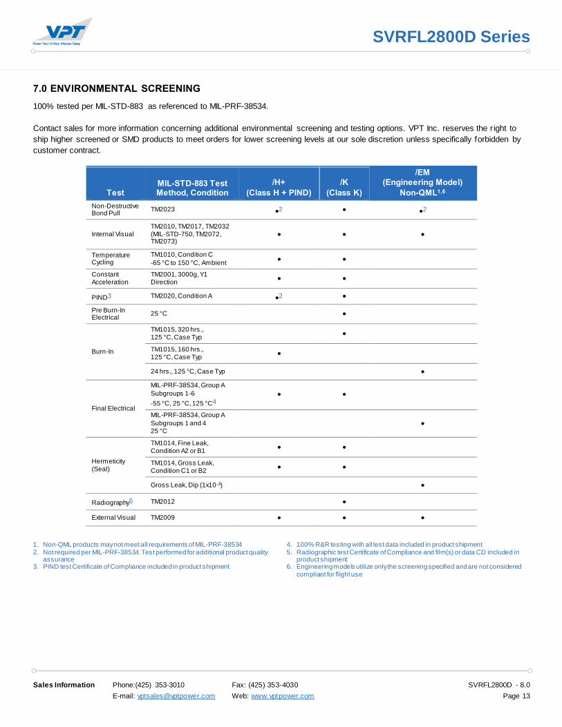
7.0 ENVIRONMENTAL SCREENING
100% tested per MIL-STD-883 as referenced to MIL-PRF-38534.
Contact sales for more information concerning additional environmental screening and testing options. VPT Inc. reserves the r ight to
ship higher screened or SMD products to meet orders for lower screening levels at our sole discretion unless specifically forbidden by
customer contract.
Test MIL-STD-883 Test Method, Condition
/H+
(Class H + PIND)
/K
(Class K)
/EM
(Engineering Model)
Non-QML1,6
Non-Destructive Bond Pull
TM2023 2 2
Internal Visual TM2010, TM2017, TM2032 (MIL-STD-750, TM2072, TM2073)
Temperature Cycling
TM1010, Condition C
-65 °C to 150 °C, Ambient
Constant Acceleration
TM2001, 3000g, Y1 Direction
PIND3 TM2020, Condition A 2
Pre Burn-In Electrical
25 °C
Burn-In
TM1015, 320 hrs., 125 °C, Case Typ
TM1015, 160 hrs., 125 °C, Case Typ
24 hrs., 125 °C, Case Typ
Final Electrical
MIL-PRF-38534, Group A
Subgroups 1-6
-55 °C, 25 °C, 125 °C4
MIL-PRF-38534, Group A
Subgroups 1 and 4 25 °C
Hermeticity (Seal)
TM1014, Fine Leak, Condition A2 or B1
TM1014, Gross Leak, Condition C1 or B2
Gross Leak, Dip (1x10⁻³)
Radiography5 TM2012
External Visual TM2009
1. Non-QML products may not meet all requirements of MIL-PRF-38534 2. Not required per MIL-PRF-38534. Test performed for additional product quality
assurance 3. PIND test Certificate of Compliance included in product shipment
4. 100% R&R testing with all test data included in product shipment 5. Radiographic test Certificate of Compliance and film(s) or data CD included in
product shipment 6. Engineering models utilize only the screening specified and are not considered
compliant for flight use
Sales Information Phone:(425) 353-3010 Fax: (425) 353-4030 SVRFL2800D - 8.0
E-mail: [email protected] Web: www.vptpower.com Page 14
SVRFL2800D Series
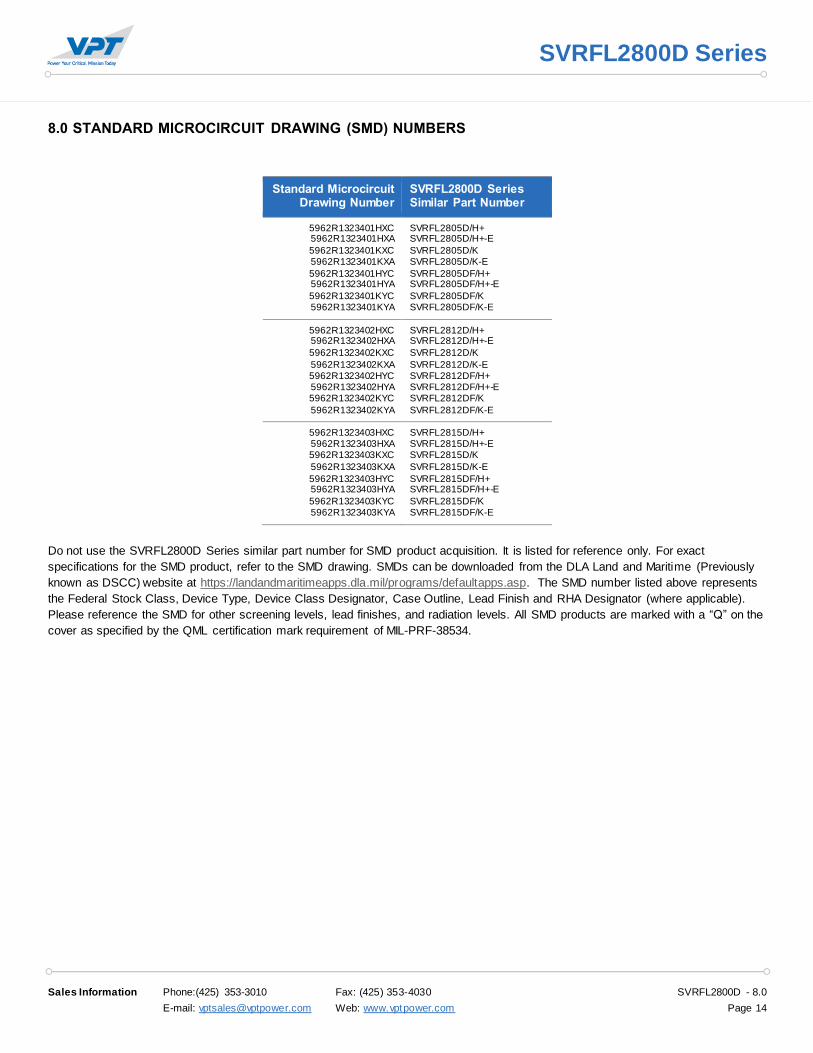
8.0 STANDARD MICROCIRCUIT DRAWING (SMD) NUMBERS
Standard Microcircuit Drawing Number
SVRFL2800D Series Similar Part Number
5962R1323401HXC 5962R1323401HXA
5962R1323401KXC 5962R1323401KXA
5962R1323401HYC 5962R1323401HYA
5962R1323401KYC 5962R1323401KYA
SVRFL2805D/H+ SVRFL2805D/H+-E
SVRFL2805D/K SVRFL2805D/K-E
SVRFL2805DF/H+ SVRFL2805DF/H+-E
SVRFL2805DF/K SVRFL2805DF/K-E
5962R1323402HXC 5962R1323402HXA
5962R1323402KXC
5962R1323402KXA 5962R1323402HYC 5962R1323402HYA 5962R1323402KYC
5962R1323402KYA
SVRFL2812D/H+ SVRFL2812D/H+-E
SVRFL2812D/K
SVRFL2812D/K-E SVRFL2812DF/H+ SVRFL2812DF/H+-E SVRFL2812DF/K
SVRFL2812DF/K-E
5962R1323403HXC 5962R1323403HXA 5962R1323403KXC
5962R1323403KXA
5962R1323403HYC 5962R1323403HYA
5962R1323403KYC 5962R1323403KYA
SVRFL2815D/H+ SVRFL2815D/H+-E SVRFL2815D/K
SVRFL2815D/K-E
SVRFL2815DF/H+ SVRFL2815DF/H+-E
SVRFL2815DF/K SVRFL2815DF/K-E
Do not use the SVRFL2800D Series similar part number for SMD product acquisition. It is listed for reference only. For exact
specifications for the SMD product, refer to the SMD drawing. SMDs can be downloaded from the DLA Land and Maritime (Previously
known as DSCC) website at https://landandmaritimeapps.dla.mil/programs/defaultapps.asp. The SMD number listed above represents
the Federal Stock Class, Device Type, Device Class Designator, Case Outline, Lead Finish and RHA Designator (where applicable).
Please reference the SMD for other screening levels, lead finishes, and radiation levels. All SMD products are marked with a “Q” on the
cover as specified by the QML certification mark requirement of MIL-PRF-38534.
Sales Information Phone:(425) 353-3010 Fax: (425) 353-4030 SVRFL2800D - 8.0
E-mail: [email protected] Web: www.vptpower.com Page 15
SVRFL2800D Series
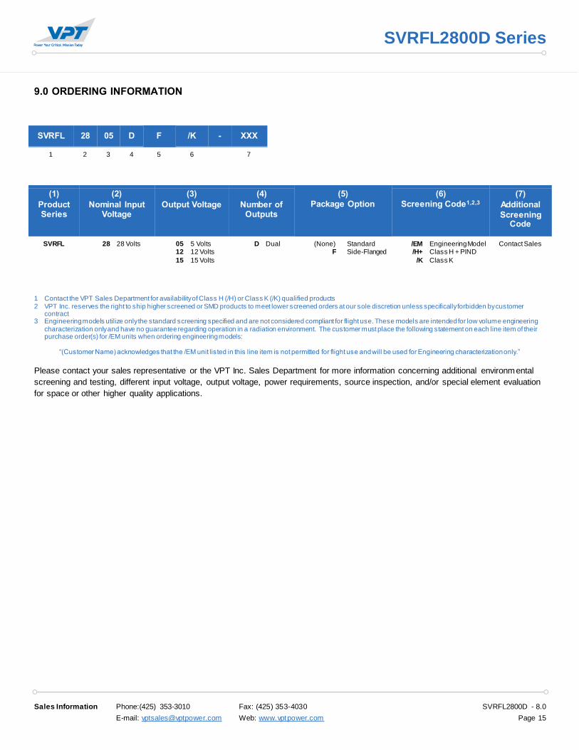
9.0 ORDERING INFORMATION
SVRFL 28 05 D F /K - XXX
1 2 3 4 5 6 7
(1)
Product Series
(2)
Nominal Input Voltage
(3)
Output Voltage
(4)
Number of Outputs
(5)
Package Option
(6)
Screening Code1,2,3
(7)
Additional
Screening Code
SVRFL 28 28 Volts 05 12
15
5 Volts 12 Volts
15 Volts
D Dual (None) F
Standard Side-Flanged
/EM /H+
/K
Engineering Model Class H + PIND
Class K
Contact Sales
1 Contact the VPT Sales Department for availability of Class H (/H) or Class K (/K) qualified products 2 VPT Inc. reserves the right to ship higher screened or SMD products to meet lower screened orders at our sole discretion unless specifically forbidden by customer
contract 3 Engineering models utilize only the standard screening specified and are not considered compliant for flight use. These models are intended for low volume engineering
characterization only and have no guarantee regarding operation in a radiation environment. The customer must place the following statement on each line item of their purchase order(s) for /EM units when ordering engineering models:
“(Customer Name) acknowledges that the /EM unit listed in this line item is not permitted for flight use and will be used for Engineering characterization only.”
Please contact your sales representative or the VPT Inc. Sales Department for more information concerning additional environmental
screening and testing, different input voltage, output voltage, power requirements, source inspection, and/or special element evaluation
for space or other higher quality applications.
Sales Information Phone:(425) 353-3010 Fax: (425) 353-4030 SVRFL2800D - 8.0
E-mail: [email protected] Web: www.vptpower.com Page 16
SVRFL2800D Series
10.0 CONTACT INFORMATION
To request a quotation or place orders please contact your sales representative or the VPT, Inc. Sales Department at:
Phone: (425) 353-3010
Fax: (425) 353-4030
E-mail: [email protected]
All information contained in this datasheet is believed to be accurate, however, no responsibility is assumed for possible errors or
omissions. The products or specifications contained herein are subject to change without notice.
11.0 ADDITIONAL INFORMATION
Visit the VPT website for additional technical resources, including:
Product Catalogs Application Notes and White Papers
Technical Video Labs Additional Products For Avionics/Military,
Hi-Rel COTS, and Space Applications


![13 37 19 C ) 10 No. f:] INH RFP SIM EB P ZAPAS INH RFP SM ... · 13 37 19 c ) 10 no. f:] inh rfp sim eb p zapas inh rfp sm eb p zap as inh rfp sm eb p zapas ) ) ) 9 th 10 e vm 1 inh](https://img.pdfslide.us/doc/110x75/5f984b500cbca115882bde59/13-37-19-c-10-no-f-inh-rfp-sim-eb-p-zapas-inh-rfp-sm-13-37-19-c-10-no.jpg)