Embed Size (px)
Citation preview

Thesis for the degree of Doctor of Philosophy
Modelling and Design of
High-Power HBV Multipliers
Mattias Ingvarson
Microwave Electronics LaboratoryDepartment of Microtechnology and Nanoscience
Chalmers University of TechnologyGoteborg, Sweden 2004

Modelling and Design ofHigh-Power HBV MultipliersMATTIAS INGVARSONISBN 91-7291-531-5
c©MATTIAS INGVARSON, 2004
Doktorsavhandlingar vid Chalmers tekniska hogskolaNy serie nr 2213ISSN 0346-718X
Technical report MC2-11ISSN 1652-0769Chalmers University of TechnologyDepartment of Microtechnology and Nanoscience (MC2)Microwave Electronics LaboratorySE–412 96 Goteborg, SwedenPhone: +46–(0)31–772 10 00
Printed in Sweden byVasastadens Bokbinderi ABGoteborg, Sweden, November 2004

Dedicated to the centenary of IFK Goteborg

iv

Modelling and Design ofHigh-Power HBV MultipliersMattias IngvarsonDepartment of Microtechnology and NanoscienceChalmers University of Technology
Abstract
This thesis deals with symmetric varactor frequency multipliers for millime-tre and sub-millimetre wave applications. Much of the material presentedis general and applicable to any type of (symmetric) varactor, but the focusis on the heterostructure barrier varactor (HBV).The basic function and principles of HBVs are explained. This includes cur-rent transport mechanisms, elastance modulation and the important para-sitic series resistance. Various epitaxial material layer structures employedfor HBVs are compared, followed by a description of HBV processing tech-niques and different device geometries. The focus is then directed towardsmodelling high-power devices and a closely related investigation of thermallimitations and models for HBVs. The thermal properties are important inthe subsequent section dealing with the design of HBV layer structures.HBV frequency multipliers are treated in the last section. Basic multiplierdesign considerations are discussed, followed by a review of the most com-mon HBV multiplier topologies. Finally, HBV multiplier measurements aredescribed and state-of-the-art results are presented.
Keywords: heterostructure barrier varactor, frequency multiplier, varactordiode, semiconductor, thermal limitations, millimetre and sub-millimetrewave power source.
v

vi

Preface
This thesis sums up my work as a PhD student at the Microwave Electron-ics Laboratory at Chalmers 1999-2004. During these years I have had thepleasure to work within the HBV-group under the supervision of Erik Koll-berg and Jan Stake. The first two years I was devoted to device fabricationin the old III-V process laboratory. This lab was then closed due to themove to the new MC2 facility, and as a result no fabrication was possiblefor about one and a half years. I therefore switched focus towards the de-sign and modelling of HBV materials and devices, which is the main topicof the thesis. I have had the opportunity to visit several conferences andto collaborate with colleagues from all over the world, and this has been agreat experience for me. Particularly, I have enjoyed the numerous visits tothe Rutherford Appleton Laboratory, UK, where we work closely togetherwith the Millimetre Wave Technology Group.
Goteborg, November 15, 2004
Mattias Ingvarson
vii

viii

List of publications
Appended papers
This thesis is based on the following papers:
A. M. Ingvarson, B. Alderman, A. Ø. Olsen, J. Vukusic, and J. Stake,“Thermal constraints for heterostructure barrier varactors”,IEEE Elec-tron Device Letters, vol. 25, no. 11, pp. 713-715, 2004.
B. M. Ingvarson, A. Ø. Olsen, and J. Stake, “Design and analysis of500 GHz heterostructure barrier varactor quintuplers”, in Proceedingsof the 14th International Symposium on Space Terahertz Technology,2003.
C. M. Ingvarson, J. Vukusic, A. Ø. Olsen, T. A. Emadi, and J. Stake,“An electro-thermal HBV model”, manuscript, 2004.
D. T. Bryllert, A. Ø. Olsen, J. Vukusic, T. A. Emadi, M. Ingvarson, J.Stake, and D. Lippens, ”An 11% efficiency 100-GHz InP-based hetero-structure barrier varactor quintupler”, submitted to Electronics Let-ters, 2004.
E. A. Ø. Olsen, M. Ingvarson, B. Alderman, and J. Stake, “A 100 GHzHBV frequency quintupler using microstrip elements”, IEEE Micro-wave and Wireless Component Letters, vol. 14, no. 10, pp. 493-495,2004.
F. A. Ø. Olsen, M. Ingvarson, and J. Stake, “A low cost fixed tuned F-band HBV frequency tripler”, in IEEE MTT-S International Micro-wave Symposium Digest, pp. 899-902, 2003.
G. L. Dillner, W. Strupinski, S. Hollung, C. Mann, J. Stake, M. Beardsley,M. Ingvarson, and E. Kollberg, “Heterostructure barrier varactors oncopper substrates for frequency multiplers”, in Proceedings of GHz2000, pp. 51-54, 2000.
ix

Other papers
The following papers are not included in the thesis due to an overlap incontent or a content going beyond the scope of this thesis:
1. J. Stake, L. Dillner and M. Ingvarson, “Fabrication and characterisa-tion of heterostructure barrier varactor diodes”, Chalmers Universityof Technology, Department of Microwave Technology, Goteborg, Tech-nical Report No. 29 1996, Revised April 2000.
2. J. Stake, C. Mann, L. Dillner, S. Jones, S. Hollung, M. Ingvarson,H. Mohamed, B. Alderman, and E. Kollberg, “Improved diode geom-etry for planar heterostructure barrier varactors”, in Proceedings ofthe 10th International Symposium on Space Terahertz Technology, pp.485-491, 1999.
3. S. Hollung, J. Stake, L. Dillner, M. Ingvarson, and E. Kollberg,“Adistributed heterostructure barrier varactor frequency tripler”, IEEEMicrowave and Guided Wave Letters, vol 48, no. 4, pp. 24-26, 2000.
4. M. Ingvarson, L. Dillner, S. Hollung, E. Kollberg, C. Mann, andJ. Stake, “Computer controlled measurements on millimetre and sub-millimetre wave varactor multipliers”, in Proceedings of GHz 2000, pp.297-300, 2000.
5. S. Hollung, J. Stake, L. Dillner, M. Ingvarson, and E. Kollberg, “Novelheterostructure barrier varactor multipliers for millimeter-wave powergeneration”, in Proceedings of GHz 2000, pp. 71-74, 2000.
6. L. Dillner, S. Hollung, M. Ingvarson, E. Kollberg, W. Strupinski,C. Mann, and J. Stake, “High efficiency HBV multipliers for millime-ter wave generation”, in Proceedings of the 13th International Confer-ence on Microwaves, Radar and Wireless Communications, pp. 47-54,2000.
7. W. Strupinski, L. Dillner, J. Sass, K. Kosiel, J. Stake, M. Ingvarson,R. Jakiela “MOVPE strain layers - growth and application”, Journalof Crystal Growth, vol 221, pp. 20-25, 2000.
8. L. Dillner, M. Ingvarson, E. Kollberg, and J. Stake, “Heterostructurebarrier varactor multipliers”, in Proceedings of GaAs 2000, pp. 197-200, 2000.
9. J. Stake, M. Ingvarson, L. Dillner, and E. Kollberg, “Progress inheterostructure barrier varactor frequency multipliers”, in Proceedingsof the 8th International Conference on Terahertz Electronics, pp. 141-144, 2000.
x

10. L. Dillner, M. Ingvarson, E. Kollberg, and J. Stake, “High efficiencyHBV multipliers for millimetre wave generation”, in Terahertz Sourcesand Systems, NATO ASI book series, Kluwer Academic Publishers,2001.
11. B. Alderman, J. Stake, L. Dillner, D. P. Steenson, M. Ingvarson,E. Kollberg, C. Mann, and J. Chamberlain, “A new pillar geometryfor heterostructure barrier varactor diodes”, in Proceedings of the 12thInternational Symposium on Space Terahertz Technology, pp. 330-339,2001.
12. M. Ingvarson, L. Dillner, W. Strupinski, and J. Stake, “Design ofmaterial structures for heterostructure barrier varactors”, presentedat 19th Nordic Semiconductor Meeting, 2001.
13. A. Ø. Olsen, J. Stake, M. Ingvarson, D. P. Steenson and S. Iezekiel,“A new waveguide integrated microstrip heterostructure barrier varac-tor (HBV) frequency tripler”, in Proceedings of the 9th InternationalConference on Terahertz Electronics, 2001.
14. M. Ingvarson, A. Ø. Olsen, B. Alderman, and J. Stake, “ Hetero-structure barrier varactor frequency multipliers: materials, devices andcircuits”, in Proceedings of GHz 2001, 2001.
15. A. Ø. Olsen, S. Kazemi, M. Ingvarson, E. Kollberg, and J. Stake,“Planar HBV triplers and quintuplers for millimetre wavelengths”, inProceedings of the 3rd ESA Workshop on Millimetre Wave Technologyand Applications, pp. 157-162, 2003.
16. A. Laisne, B. Alderman, D. Matheson, B. Ellison, A. Ø. Olsen, M. In-gvarson, and J. Stake “A 500 GHz HBV quintupler”, presented atTerahertz Electronics, 2003.
17. M. Ingvarson, A. Ø. Olsen, E. Kollberg, and J. Stake, “Design,analysis and modelling of heterostructure barrier varactors for sub-millimetre wave frequency quintuplers”, in Proceedings of GHz 2003,2003.
18. A. Ø. Olsen, M. Ingvarson, E. Kollberg, and J. Stake, “Hetero-structure barrier varactor frequency triplers and quintuplers for THzelectronics” , in Proceedings of GHz 2003, 2003.
19. A. Emadi, J. Vukusic, M. Ingvarson, T. Bryllert, A. Ø. Olsen, E. Koll-berg, and J. Stake, ”High power HBV multipliers for F- and G- bandapplications”, in Proceedings of the Joint 29th IRMMW2004 / 12thTHz2004, pp. 319-320, 2004.
xi

xii

Acknowledgement
Three people share the main responsibility for recruiting me to a PhD stu-dent position in microwave electronics at Chalmers. These are, in chrono-logical order, Lennart Lundgren, Erik Kollberg and Jan Stake.I want to thank Lennart for his outstanding lectures, for introducing meto the field of microwave electronics, and for being a source of inspirationthroughout my years at Chalmers.Erik employed me as a graduate student 10 years after he invented the de-vice that I have spent the last 5 years exploring. It has been a pleasure toshare his great experience and I especially appreciate his support and adviceduring the last year of research and the writing of this thesis.I had the intention to finish my master’s thesis project, with Jan as thesupervisor, as soon as possible and then leave Chalmers. Jan, however, hadother plans. He used my weakness for English pubs to entice me to continueat Chalmers to work in the HBV factory during the days, and, as it turnedout, with child-minding, house-painting, transporting junk etc. during theremaining hours. I am very grateful for his support, inspiration and friend-ship throughout these years.
None of my research achivements, if any, would have been possible with-out the help and support from my HBV colleagues at Chalmers. I ammost grateful to them all: Lars Dillner, Stein Hollung, Arne Øistein Olsen,Shada Kazemi, Arezoo Emadi, Josip Vukusic and Tomas Bryllert.
I have really appreciated all visits to, and cooperation with, the RutherfordAppleton Laboratory. I have received great hospitality and help, especiallyfrom the following, to whom I am deeply obliged: Dave Matheson, ChrisMann, Byron Alderman, John Spencer, Tony Jones, Dave Wilsher, MatthewBeardsley, Brian Landowski and Steve Deane.
Bobby Weikle from the University of Virginia spent a sabbatical year withus at Chalmers, and it was a pleasure to share his great knowledge, ideasand expertise concerning microwave circuits.
I have enjoyed the support and camaraderie from numerous colleagues atChalmers: Jan Andersson, Stefan Davidsson, Vincent Desmaris, JoakimEriksson, Christian Fager, Catharina Forssen, Hans Hjelmgren,
xiii

Lars-Olof Landen, Bente Larsson, Anders Mellberg, Harald Merkel, NiklasRorsman, Par Rundqvist, Piotr Starski, Mahdad Sadeghi, Jorgen Stenar-son, Klas Yhland, Anders Olausson and Herbert Zirath. Special thanks toUlf Jordan for help and advice with LATEX .
Anyone whom I have forgotten to acknowledge properly: Please accept mysincere apologies.
Finally, I would like to thank my friends and family for support.
This work has been supported by the Swedish Foundation for Strategic Re-search (SSF), the European Space Agency (ESA), and the Swedish DefenceResearch Agency (FOI).
xiv

Contents
Abstract v
Publications ix
Acknowledgement xiii
1 Introduction 1
2 Varactors 32.1 Basic concepts . . . . . . . . . . . . . . . . . . . . . . . . . . 3
2.1.1 Manley-Rowe formulae . . . . . . . . . . . . . . . . . . 32.2 Pure varactor model . . . . . . . . . . . . . . . . . . . . . . . 42.3 Practical varactors . . . . . . . . . . . . . . . . . . . . . . . . 42.4 Pumping . . . . . . . . . . . . . . . . . . . . . . . . . . . . . . 52.5 Symmetric varactor frequency multipliers . . . . . . . . . . . 6
2.5.1 Conversion efficiency . . . . . . . . . . . . . . . . . . . 62.5.2 Elastance models . . . . . . . . . . . . . . . . . . . . . 62.5.3 Losses caused by conduction current . . . . . . . . . . 8
3 Heterostructure barrier varactors 93.1 Principle of operation . . . . . . . . . . . . . . . . . . . . . . 9
3.1.1 Equivalent circuit models . . . . . . . . . . . . . . . . 113.1.2 Capacitance-voltage characteristics . . . . . . . . . . . 123.1.3 Current-voltage characteristics . . . . . . . . . . . . . 143.1.4 Series resistance . . . . . . . . . . . . . . . . . . . . . 163.1.5 Electro-thermal HBV modelling . . . . . . . . . . . . . 183.1.6 Physical modelling of HBVs . . . . . . . . . . . . . . . 18
3.2 Material systems . . . . . . . . . . . . . . . . . . . . . . . . . 183.2.1 GaAs/AlGaAs on GaAs . . . . . . . . . . . . . . . . . 203.2.2 InGaAs/InAlAs on InP . . . . . . . . . . . . . . . . . 203.2.3 InAs/AlSb on InAs . . . . . . . . . . . . . . . . . . . . 213.2.4 Metamorphic InGaAs/InAlAs on GaAs . . . . . . . . 213.2.5 Wide band-gap materials: AlGaN/GaN . . . . . . . . 223.2.6 Ferroelectric varactors . . . . . . . . . . . . . . . . . . 22
xv
3.2.7 Si/SiO2 on Si . . . . . . . . . . . . . . . . . . . . . . . 223.3 Practical HBVs . . . . . . . . . . . . . . . . . . . . . . . . . . 22
3.3.1 Fabrication . . . . . . . . . . . . . . . . . . . . . . . . 223.3.2 Whisker-contacted geometries . . . . . . . . . . . . . . 223.3.3 Planar geometries . . . . . . . . . . . . . . . . . . . . 243.3.4 Pillar geometries . . . . . . . . . . . . . . . . . . . . . 243.3.5 Integrated devices . . . . . . . . . . . . . . . . . . . . 263.3.6 High-power devices . . . . . . . . . . . . . . . . . . . . 26
3.4 Thermal properties . . . . . . . . . . . . . . . . . . . . . . . . 273.4.1 Thermal estimations and models . . . . . . . . . . . . 28
3.5 Design of HBV layer structures . . . . . . . . . . . . . . . . . 28
4 HBV frequency multipliers 314.1 Design of HBV multipliers . . . . . . . . . . . . . . . . . . . . 31
4.1.1 Optimum impedance levels . . . . . . . . . . . . . . . 324.1.2 Noise in varactor multipliers . . . . . . . . . . . . . . . 33
4.2 HBV tripler and quintupler topologies . . . . . . . . . . . . . 344.2.1 Crossed waveguide multipliers . . . . . . . . . . . . . . 354.2.2 Distributed multipliers . . . . . . . . . . . . . . . . . . 364.2.3 Waveguide-integrated microstrip multipliers . . . . . . 364.2.4 Quasi-optical multipliers . . . . . . . . . . . . . . . . . 37
4.3 Frequency multiplier measurements . . . . . . . . . . . . . . . 374.3.1 Measurements on waveguide multipliers . . . . . . . . 374.3.2 Cooled measurements . . . . . . . . . . . . . . . . . . 40
4.4 HBV multiplier performance . . . . . . . . . . . . . . . . . . . 40
5 Summary of appended papers 43
xvi

Chapter 1
Introduction
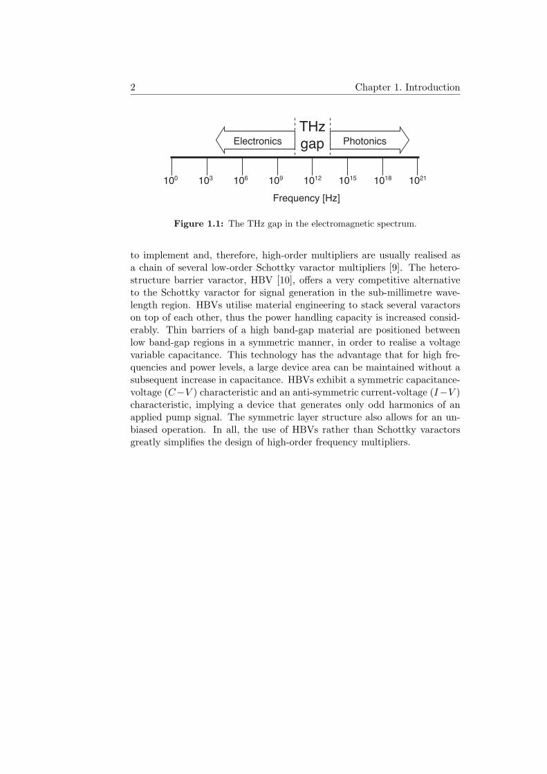
Terahertz technology, defined as technology using frequencies from about100 GHz to several 3 THz, is gradually maturing and already used in manyapplications [1]. The main applications today are within science, particularlyradio astronomy. Applications under development or still at a planning stageare high-speed wireless networks, short-range high-resolution radar systems,medical and biological imaging, high-speed inter-satellite communication,earth environment monitoring, military applications, and surveillance sys-tems, notably security systems. Most such applications crucially depend onthe availability of reasonably inexpensive, lightweight and compact sourcesand detectors. However, as the frequency approaches 1 THz, the outputpower for both electronic and photonic signal sources drops rapidly. This iscommonly referred to as the THz gap, cf Figure 1.1. Traditional fundamentalsignal sources are backward-wave oscillators (BWO) that can generate a fewmW at 1.5 THz, and optically pumped lasers for spot frequencies between0.5 and at least 5 THz with output power in the mW range. However, thesesources are heavy, bulky and very expensive. A potential replacement is thequantum cascade laser (QCL) [2] which works very well down to about 3THz [3], [4] and has the potential to extend the operation down to 1 THz [5].The major problem is that the present technology requires cryogenic coolingat long wavelengths, which makes QCLs awkward to use. Another approachis photomixing [6], which has shown promising results between 100 GHz and1 THz, but the output power has only been in the µW range in the bestcase, apart from a recent demonstration of 20 mW at 100 GHz [7].
The most promising approach to reach the terahertz frequency rangewith a solid state source is to use a frequency multiplier. Traditionally,this has been accomplished with a reverse-biased Schottky diode [8]. How-ever, the power handling capability of the Schottky device is limited bythe device area, which has to be very small at high operating frequenciesto allow for manageable impedance levels. From a circuit point of view,higher harmonic multiplication factors (> × 3) become increasingly difficult
1
2 Chapter 1. Introduction
100 103 1021101810151012109106
Frequency [Hz]
Electronics PhotonicsTHzgap
Figure 1.1: The THz gap in the electromagnetic spectrum.
to implement and, therefore, high-order multipliers are usually realised asa chain of several low-order Schottky varactor multipliers [9]. The hetero-structure barrier varactor, HBV [10], offers a very competitive alternativeto the Schottky varactor for signal generation in the sub-millimetre wave-length region. HBVs utilise material engineering to stack several varactorson top of each other, thus the power handling capacity is increased consid-erably. Thin barriers of a high band-gap material are positioned betweenlow band-gap regions in a symmetric manner, in order to realise a voltagevariable capacitance. This technology has the advantage that for high fre-quencies and power levels, a large device area can be maintained without asubsequent increase in capacitance. HBVs exhibit a symmetric capacitance-voltage (C−V ) characteristic and an anti-symmetric current-voltage (I−V )characteristic, implying a device that generates only odd harmonics of anapplied pump signal. The symmetric layer structure also allows for an un-biased operation. In all, the use of HBVs rather than Schottky varactorsgreatly simplifies the design of high-order frequency multipliers.

Chapter 2
Varactors
This chapter reviews fundamental varactor theory and presents conceptsand definitions that form the basis for the description and modelling ofHBV devices and multipliers in the following chapters. The presentation isstrongly inspired by the monumental work by Penfield and Rafuse [11]. Forfurther reading, see also [12,13].
2.1 Basic concepts
A varactor is a device that exhibits a voltage variable, implicitly capaci-tive, reactance. A varactor is typically a semiconductor diode, which can beused for harmonic generation, frequency conversion, parametric amplifica-tion, detection and voltage-variable tuning [11]. During operation, currentsof many frequencies can be present in the varactor. Some of these currentsare useful inputs or outputs, while some are idlers. Idlers can, however, benecessary for optimum operation of the device.
2.1.1 Manley-Rowe formulae
The Manley-Rowe formulae [14] relate power flowing into and out of nonlin-ear reactances. The relations apply to ideal, i. e. loss-less, varactors wherecurrent and voltage are assumed to exist at frequencies mf1 +nf2, where mand n are integers. The formulae are
∞∑m=1
∞∑n=−∞
mPm,n
nf1 + mf2= 0 (2.1)
∞∑m=−∞
∞∑n=1
nPm,n
nf1 + mf2= 0. (2.2)
Pm,n is the average power flowing into the varactor at the frequency mf1 +nf2. For a frequency multiplier all frequencies are harmonics of only one
3
4 Chapter 2. Varactors
frequency, f1, thus m = 0, and the Manley-Rowe relations become P1 +Pn = 0. That is, if the circuit is designed so that only real power can flowat the input frequency f1 and at the output frequency nf1, the Manley-Rowe formulae predict a conversion efficiency of 100%. It should be noted,however, that the Manley-Rowe formulae do not take any DC power intoaccount. This means that the power at any output frequency nf1 cannot beincreased by supplying DC power.
2.2 Pure varactor model
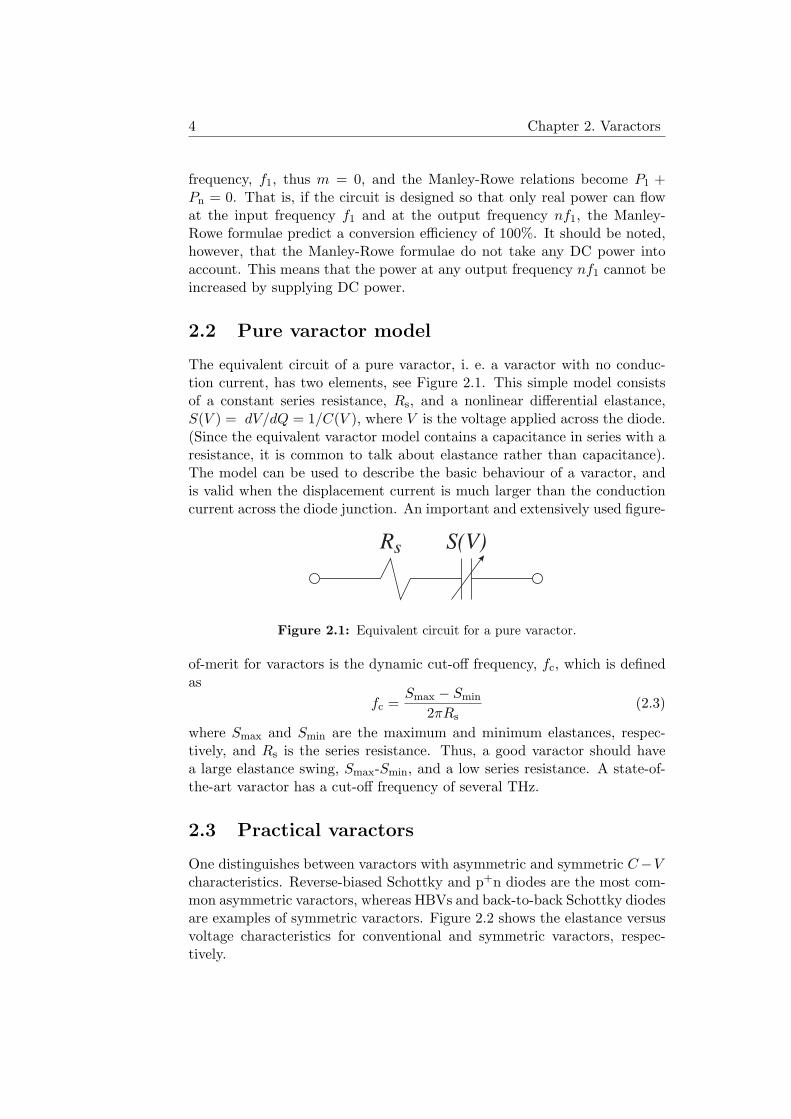
The equivalent circuit of a pure varactor, i. e. a varactor with no conduc-tion current, has two elements, see Figure 2.1. This simple model consistsof a constant series resistance, Rs, and a nonlinear differential elastance,S(V ) = dV/dQ = 1/C(V ), where V is the voltage applied across the diode.(Since the equivalent varactor model contains a capacitance in series with aresistance, it is common to talk about elastance rather than capacitance).The model can be used to describe the basic behaviour of a varactor, andis valid when the displacement current is much larger than the conductioncurrent across the diode junction. An important and extensively used figure-
S(V)Rs
Figure 2.1: Equivalent circuit for a pure varactor.
of-merit for varactors is the dynamic cut-off frequency, fc, which is definedas
fc =Smax − Smin
2πRs(2.3)
where Smax and Smin are the maximum and minimum elastances, respec-tively, and Rs is the series resistance. Thus, a good varactor should havea large elastance swing, Smax-Smin, and a low series resistance. A state-of-the-art varactor has a cut-off frequency of several THz.
2.3 Practical varactors
One distinguishes between varactors with asymmetric and symmetric C−Vcharacteristics. Reverse-biased Schottky and p+n diodes are the most com-mon asymmetric varactors, whereas HBVs and back-to-back Schottky diodesare examples of symmetric varactors. Figure 2.2 shows the elastance versusvoltage characteristics for conventional and symmetric varactors, respec-tively.

2.4. Pumping 5
Smax=1/Cmin
Smin=1/Cmax
S(V)
-Vmax 0 Vmax
S(V)
Smax=1/Cmin
-Vmax 0 φb
Figure 2.2: Elastance versus voltage for (left) a conventional (asymmetric) var-actor and (right) a symmetric varactor.
2.4 Pumping
The process where a large current at an angular pump frequency ωp = 2πfp
is passed through the varactor is called pumping. This is the normal mode ofoperation for a varactor in a frequency multiplier. During a pump cycle, thevaractor behaves as a time-varying elastance, S(t), and power is dissipatedin the series resistance. The voltage across the pure varactor in Figure 2.1is then
v(t) = Rsi(t) +∫
S(t)i(t)dt. (2.4)
The boundary conditions to (2.4) are equations describing how the varactoris terminated at the harmonics involved. These equations, however, are moreconveniently described in the frequency domain. In a frequency multiplieronly frequencies that are multiples of the pump frequency, i. e. k ·ωp, k ∈ N,are present. The voltage, current and differential elastance can therefore bewritten as Fourier series:
v(t) =∞∑
k=−∞Vke
jkωpt, (2.5)
i(t) =∞∑
k=−∞Ike
jkωpt (2.6)
and
S(t) =∞∑
k=−∞Ske
jkωpt, (2.7)
where V−k = V ∗k , I−k = I∗k and S−k = S∗k as v(t), i(t) and S(t) are realquantities. Thus, the Fourier coefficients of V can be written
Vk = RsIk +1
jkωp
∞∑l=−∞
IlSk−l. (2.8)
6 Chapter 2. Varactors
2.5 Symmetric varactor frequency multipliers
This section reviews some basic concepts applicable to symmetric varactorfrequency multipliers, notably HBV multipliers.
2.5.1 Conversion efficiency
The conversion efficiency η is defined as the power delivered to the load at thedesired output frequency, n×fp, divided by the available input power at fp.The maximum conversion efficiency for varactor multipliers is related to theratio of the pump frequency fp and the dynamic cut-off frequency fc [11,15].The following empirical expression is useful for initial estimations [16],[PaperB]:
η =100
1 + α
(n · fp
3 · fc
)β, (2.9)
where α and β can be extracted from large-signal simulations for various(HBV) devices and circuit conditions. For fp/fc < 0.2, we typically findα = 200 and β = 1.5 for HBV triplers [16].
2.5.2 Elastance models
It is of interest to investigate how the shape of elastance-voltage (S − V )characteristics influence the conversion efficiency of varactor frequency mul-tipliers. In order to facilitate such studies it is advantageous to use simple,generally defined S−V models. One such model is the cubic varactor modelfor the voltage V as a function of the stored charge Q in the varactor [17],which is based on the third-order voltage-charge model suggested by Tanget al. [18]. The cubic model can be extended to a fifth degree polynomialmodel to allow for varying the shape of the S − V characteristics:
V (Q) = SminQ + (Smax − Smin)(
ξQ3
Q2max
+ χQ5
Q4max
)(2.10)
whereQmax =
Vmax
Smin + (Smax − Smin)(ξ + χ). (2.11)
Qmax is the charge stored in the varactor at the maximum voltage, Vmax,during a pump cycle, and ξ and χ are fitting coefficients. For (2.10) todescribe an HBV correctly, the differential elastance must increase mono-tonically with increasing charge. This constraint gives two extreme cases forfixed values of Smin and Smax, denoted flat S − V and sharp S − V , respec-tively. ξ and χ for the three elastance models mentioned are summarisedin Table 2.1. Figure 2.3 displays elastance waveforms obtained from (2.10)with the coefficients taken from Table 2.1. The sharp S−V model gives thehighest conversion efficiency in varactor multipliers [15].

2.5. Symmetric varactor frequency multipliers 7
Table 2.1: Constants for the three S − V models for (2.10).
ξ χ
Flat 0 1/5Cubic 1/3 0Sharp 2/3 -1/5
CubicFlat
Sharp
Vmax0-Vmax
S(V)Smax
Smin
Figure 2.3: S-V characteristics for the three models generated from (2.10).

8 Chapter 2. Varactors
2.5.3 Losses caused by conduction current
Any practical varactor has a non-zero conduction current, which causeslosses and thereby degrades the multiplier performance. This conductioncurrent can be modelled as a voltage dependent conductance in parallelwith the nonlinear, differential elastance of the pure varactor model, seeFigure 2.4. In this extended model, the differential elastance S(V ) has been
G(V)
Rs
S(V)-Smin Smin
Figure 2.4: Extended varactor model.
split up in two parts, where Smin is the minimum elastance which appearsat zero bias. The conductance increases with increasing bias, cf Figure 3.6,implying that the maximum conductance occurs at the maximum bias,
Gmax =Imax
Vmax. (2.12)
If the conductance is assumed to be constantly equal to the maximum value,(2.12), it is possible to estimate an upper limit of the losses caused by theconduction current. As a rule of thumb, if Gmax . ωp ·Cmin · 0.01, the extraloss introduced by Gmax is less than approximately 0.3 dB [19].

Chapter 3
Heterostructure barriervaractors
The heterostructure barrier varactor (HBV) was invented in 1989 by ErikKollberg, [10], as a spin-off from the research on resonant tunnelling devices.An HBV is a symmetric device composed of a high band-gap semiconductor(barrier) that is surrounded by low band-gap semiconductors (modulationlayers), see Figure 3.1, for typical dimensions see Table 3.2. The first HBVshad only one barrier and were therefore referred to as single-barrier varac-tors, SBVs. Another obsolete term that is sometimes encountered in theliterature is quantum-barrier varactors, QBVs. Practical HBVs typicallyhave 1-6 barriers. The layer structure is grown by molecular beam epitaxy(MBE) or metal-organic vapour phase epitaxy (MOVPE). Thanks to therapid progress in these epitaxial growth techniques during the last decade,it is now possible to grow HBV materials of high quality [20–23]. So far,HBVs have exclusively been realised in III-V material systems, althoughSi/SiO2/Si devices conceptually similar to III-V HBVs have been investi-gated to some extent [24].
3.1 Principle of operation
Consider a one-barrier HBV, i. e. one barrier symmetrically sandwiched be-tween two modulation layers. The barrier acts as a potential barrier for theelectrons, and thus prevents electron transport through the structure. Whenan external bias V is applied across the device, electrons are accumulatedat one side of the barrier and depleted at the other side, see Figure 3.2.The device thus has a voltage-dependent depletion region in the modulationlayer, implying a voltage-dependent C −V characteristic. The symmetry ofthe layer structure gives a symmetric C − V characteristic, i. e. an HBV isa symmetric varactor. The main current transport mechanisms in an HBVare thermionic emission of electrons over the barrier and electron tunnelling
9

10 Chapter 3. Heterostructure barrier varactors
substrate
Ω-contact
metal
modulationmodulation
contact
contact
barrier
Figure 3.1: CAD view of a one-barrier HBV mesa. For typical dimensions, seeTable 3.2.
b0 w+b
V
Va
barrier
depletion
accumulationE
Vb
Vc
Figure 3.2: Conduction band of a one-barrier HBV. w is the width of the depletionregion.

3.1. Principle of operation 11
through the barrier. The device temperature, applied bias and the effectiveheight and thickness of the barrier determines the dominating mechanism.In order to maximise the power handling capacity, the HBV material shouldhave several barriers stacked in series, and a relatively low doping concentra-tion in the modulation layers to increase the breakdown voltage. However,if too many barriers are used, the device temperature increases, and thisdegrades the diode’s varactor properties. For a given material structure it ispossible to estimate the maximum number of barriers that can be used with-out degrading the HBV [Paper A]. If the modulation layers are made shorterand doped more heavily, the losses and the effect of current saturation forhigh frequency applications are reduced [25,26].
3.1.1 Equivalent circuit models
The most simple equivalent circuit model for HBVs is the the pure varac-tor model presented in Figure 2.1, which can be used to describe the basicproperties. A more accurate model, useful for numerical analysis of HBVs,is the nonlinear, quasi-static model displayed in Figure 3.3. The currentsource models the leakage current through the device. A more extensive
+
Rs
Q(V) I(V)V
-
Figure 3.3: Quasi-static equivalent circuit model of an HBV.
model is displayed in Figure 3.4. This model can be extracted from mea-sured reflection coefficients [27]. Here, the dependence on temperature andfrequency is included, as well as parasitic elements. The series resistanceis frequency-dependent due to the skin effect, and voltage-dependent dueto the extension of the depletion region. The series inductance Lp modelsthe connection to the diode, i. e. bonding wire or air-bridge, and the shuntcapacitance Cp represents parasitic capacitances due to packaging.

12 Chapter 3. Heterostructure barrier varactors
+
Rs(V,T,f)
Q(V,T) I(V,T)V
-Cp
Lp
Cp
Lp
⇔
Figure 3.4: Extended quasi-static equivalent circuit model of an HBV.
3.1.2 Capacitance-voltage characteristics
The symmetric C−V characteristic of a typical HBV is shown in Figure 3.5.The appearance of the HBV capacitance can be understood by considering
Bias [V]
Cap
acita
nce
[fF/
µm
2 ]
Figure 3.5: Measured capacitance per unit area versus applied voltage for a typicalHBV diode. The material is a four-barrier InGaAs/InAlAs heterostructure on anInP substrate, CTH-ITME-1820.
the parallel plate capacitor model. The plate separation is equivalent to thesum of the barrier thickness, b, the spacer layer thickness, s, see Table 3.2,and the length of the depletion region in the modulation layer, w. Due tothe symmetric layer structure of HBVs, the differential elastance is an evenfunction of the applied voltage,
S(V ) =1
C(V )=
N
A
(b
εb+
s
εd+
w(V )εd
), (3.1)

3.1. Principle of operation 13
where N is the number of barriers, A is the device area, and εb and εd
are the dielectric constants of the barrier and modulation layer materials,respectively. Equation (3.1) is not accurate close to zero bias. w can becalculated from
w =
√2εd |Vd|
qNd, (3.2)
where Vd is the voltage across the depleted region of each modulation layer,q is the elementary charge and Nd is the doping concentration in the mod-ulation layers. The minimum elastance Smin occurs at zero bias, i. e. w=0.However, due to electron screening effects, a more accurate expression forSmin must include the extrinsic Debye length LD,
LD =
√εdkT
q2Nd, (3.3)
where k is the Boltzmann constant and T is the device temperature. Thus
Smin =N
A
(b
εb+
2s
εd+
2LD
εd
). (3.4)
The maximum elastance Smax during a pump cycle is determined by thedrive level of the HBV, defined as
drive =max(Q(t))
Qmax(3.5)
where Qmax is the charge at the turn-on voltage, Vj,max [16]. Optimumperformance is achieved with a maximum elastance swing, low conductioncurrent and drive=1. Under these conditions, the maximum elastance islimited by
Smax =N
A
(b
εb+
s
εd+
wmax
εd
)(3.6)
where wmax is the maximum extension of the depletion region, determinedby one of the following conditions:
1. Modulation layer punch-through, i. e. the modulation layer is fullydepleted so that wmax=l where l is the thickness of the modulationlayer;
2. Large electron conduction current across the barrier due to thermionicemission at high electric fields;
3. Large electron conduction current originating from impact ionisationat high electric fields;
4. Current saturation, i. e. the saturated electron velocity determines themaximum length an electron can travel during a pump cycle.

14 Chapter 3. Heterostructure barrier varactors
All four of the above conditions are valid for GaAs-based HBVs, whereascondition 2 is usually not applicable for InP-based devices due to the muchhigher effective barrier height. For condition 2, the conduction current de-pends on the effective barrier height and the electric field in the barrier [28].For condition 3, wmax can be calculated as
wmax =εdEd,max
qNd(3.7)
where Ed,max is the maximum electric field in the modulation layer at thevoltage where breakdown occurs. For condition 4, wmax can be estimated as
wmax ≈vmax
8fp(3.8)
where vmax is the saturated electron velocity [25].The Chalmers HBV model, (3.9), is a quasi-empirical expression for the
voltage V across an HBV expressed as a function of the charge Q stored inthe device [29]:
V (Q) = N
(bQ
εbA+ 2
sQ
εdA
+ sign(Q)(
Q2
2qNdεdA2+
4kT
q
(1− exp
[− |Q|
2LDAqNd
]))). (3.9)
Equation (3.9) is useful for numerical analysis of HBVs, e. g. harmonicbalance.
3.1.3 Current-voltage characteristics
The I − V characteristic of an HBV is anti-symmetric. Its appearance ismainly caused by thermionic emission of electrons over the barrier and/ortunnelling of electrons through the barrier. The device temperature, appliedbias and the height and thickness of the barrier determine which currenttransport mechanism is dominant in each situation. An I−V characteristicof a typical HBV is shown in Figure 3.6. Given a general barrier structureand adjacent modulation layers, it is possible to calculate the I −V charac-teristic with numerical techniques [30–32]. The conduction current can becalculated by solving the Poisson equation and the Schrodinger equation [33].Attempts to solve the Poisson and Schrodinger equations self-consistently foran applied AC bias have been carried out [34], but this approach is not yetfeasible for design work. Instead, empirical, quasi-static I − V models haveto be used to predict the RF performance of HBVs. For GaAs/AlGaAs onGaAs HBVs, where thermionic field emission is the dominant current trans-port mechanism, the following model can be used to calculate the conduction

3.1. Principle of operation 15
Bias [V]
Cur
rent
den
sity
[µ
A/µ
m2 ]
Figure 3.6: Measured current density versus voltage for a typical HBV diode.The material is a four-barrier InGaAs/InAlAs heterostructure on an InP substrate,CTH-ITME-1820.
current density:
Jcond,GaAs = aT 2sinh
(Eb
E0
)exp
(− φb
kT
)(3.10)
where Eb is the electric field in the barrier and a, E0 and φb are constants[29]. The constants can be extracted from Arrhenius plots of the measuredcurrent density at different temperatures. Eb can be estimated from thePoisson equation as
Eb =Ndqεdb
ε2b
√1 +2V ε2
b
Ndqεdb2N− 1
, (3.11)
or explicitly from the charge as Eb = Q/(εbA). For InGaAs/AlInAs on InPHBVs, the conduction current can be described by
Jcond,InP = a · exp
(T
T0
)sinh
(V
V0
)(3.12)
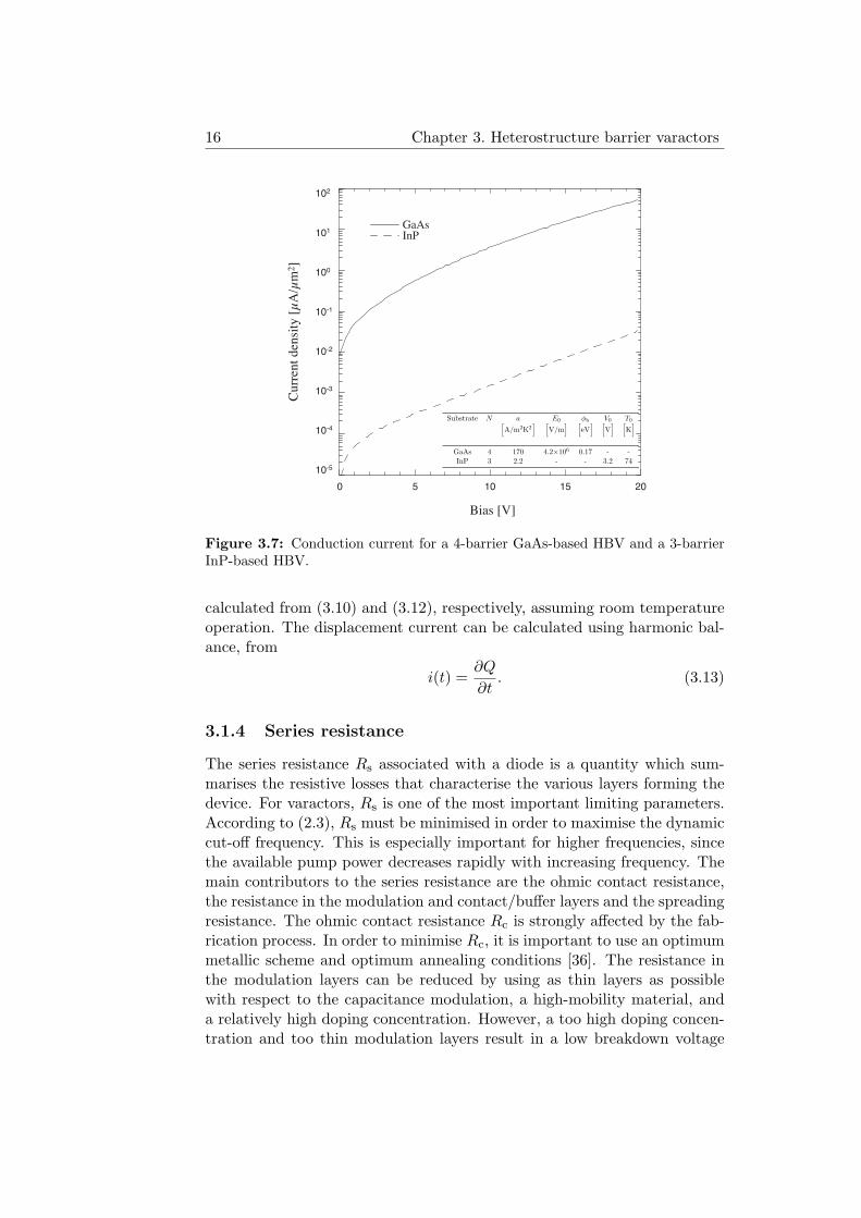
where a, T0 and V0 are constants [35]. Figure 3.7 shows a comparison be-tween the conduction current of a 4-barrier GaAs-based HBV (UVA-NRL-1174) and a 3-barrier InP-based HBV (CTH-ITME-1596). The curves where
16 Chapter 3. Heterostructure barrier varactors
0 5 10 15 20
GaAsInP
10-5
10-4
10-3
10-2
10-1
100
101
102
Bias [V]
Cur
rent
den
sity
[µ
A/µ
m2 ]
Substrate N a E0 φb V0 T0[A/m2K2
] [V/m
] [eV] [
V] [
K]
GaAs 4 170 4.2×10⁶ 0.17 - -InP 3 2.2 - - 3.2 74
Figure 3.7: Conduction current for a 4-barrier GaAs-based HBV and a 3-barrierInP-based HBV.
calculated from (3.10) and (3.12), respectively, assuming room temperatureoperation. The displacement current can be calculated using harmonic bal-ance, from
i(t) =∂Q
∂t. (3.13)
3.1.4 Series resistance
The series resistance Rs associated with a diode is a quantity which sum-marises the resistive losses that characterise the various layers forming thedevice. For varactors, Rs is one of the most important limiting parameters.According to (2.3), Rs must be minimised in order to maximise the dynamiccut-off frequency. This is especially important for higher frequencies, sincethe available pump power decreases rapidly with increasing frequency. Themain contributors to the series resistance are the ohmic contact resistance,the resistance in the modulation and contact/buffer layers and the spreadingresistance. The ohmic contact resistance Rc is strongly affected by the fab-rication process. In order to minimise Rc, it is important to use an optimummetallic scheme and optimum annealing conditions [36]. The resistance inthe modulation layers can be reduced by using as thin layers as possiblewith respect to the capacitance modulation, a high-mobility material, anda relatively high doping concentration. However, a too high doping concen-tration and too thin modulation layers result in a low breakdown voltage

3.1. Principle of operation 17
and a low maximum elastance. Therefore, there is a trade-off between highpower handling capacity and low losses. The spreading resistance is causedby the material near the anode and, at high frequencies, the skin effect hasto be included [37], which means that the diode geometry becomes impor-tant. Given the voltage-charge relationship in (3.9), the series resistance canbe expressed as [16]
R(Q) = Rs −ρdN
A
(|Q|
qNdA+ 2LD
(exp
[− |Q|
2LDAqNd
]− 1))
(3.14)
where Rs is the zero-bias intrinsic series resistance and ρd is the resistivityof the modulation layer,
ρd =1
qNdµe(Nd, T ). (3.15)
The electron low-field mobility µe(Nd, T ) can be calculated from the follow-ing empirical model [38]
µe(Nd, T ) = µmin +µmax(T0)(T0/T )θ1 − µmin
1 +
(Nd
Nref(T0)(T/T0)θ2
)λ. (3.16)
Here, µmin, µmax, Nref , λ, θ1 and θ2 are fitting parameters available for mostcommon III-V materials, and T0 = 300K. It is very difficult to measure theseries resistance. For varactors that can be probed, Rs can be extracted fromreflection coefficient measurements with a network analyser [27]. However,a sensitivity analysis [36] shows that the accuracy from an S-parameteranalysis can never be better than
∆Rs
Rs=
(Rs + Z0)2
2RsZ0∆Γ (3.17)
where Z0 is the characteristic (system-) impedance and ∆Γ is the estimatedmeasurement error in the reflection coefficient Γ. Equation (3.17) is validfor Q-values below the optimum Q-value for capacitance estimations, whichis approximately
1ωC
= Z0. (3.18)
Another way to estimate the series resistance is to combine data from contactresistance measurements with resistivity data for the semiconductors used.
At terahertz frequencies, other effects become important. The perfor-mance can be degraded by plasma resonances in the epilayers and currentsaturation. The latter effect can be modelled as an effective series resistance,which increases rapidly with increasing pump power [25].
18 Chapter 3. Heterostructure barrier varactors
3.1.5 Electro-thermal HBV modelling
In order to properly analyse and design HBV devices and circuits, especiallyfor high-power applications, it is necessary to combine electrical and ther-mal simulations. We have demonstrated the first such model, [Paper C],which automatically updates the temperature and temperature-dependentparameters as the series resistance and the conduction current. The model isimplemented in ADS from Agilent and can accurately reproduce measuredresults.
3.1.6 Physical modelling of HBVs
Physical modelling can give important information about, and insight into,the behaviour of semiconductor devices under various operating conditions.Jones et al. have developed a time-dependent numerical drift/diffusion HBVmodel, integrated with a large-signal harmonic balance circuit simulator[39–41]. In order to accurately model carrier transport at high frequencies,the effect of hot electron transport should be included. For Schottky diodes,this has been accomplished by means of Monte-Carlo simulations [42] andby including energy balance equations [30]. These techniques can also beemployed, but are still unexplored, for HBVs.
3.2 Material systems
So far, all working HBVs have been fabricated from a combination of III-Vsemiconductors. Important data for some materials of interest for HBVs ispresented in Table 3.1. The layer structures are grown with epitaxial growthtechniques, mainly molecular beam epitaxy, MBE, and metal-organic vapourphase epitaxy, MOVPE. The properties of HBV devices depend strongly onthe quality of the layer structure material. Thanks to the extensive progressin these epitaxial growth techniques during the last decade, it is now possibleto realise relatively complicated HBV materials with sufficient accuracy andquality. However, new material combinations are continuously being investi-gated, in order to find ways to minimise the series resistance and the leakagecurrent, to maximise the breakdown voltage, to improve the high frequencyproperties, etc. In principle, any symmetrical material combination with aband-gap discontinuity can be chosen. Yet, an important constraint is thatthe lattice mismatch must not be too large in order to avoid stress in thestructure. If the layer thickness of a certain material reaches the material’scritical thickness, the layer relaxes to its natural lattice constant, causingdislocations in the material. Stress also causes piezoelectric fields, whichmay alter the energy band structure, and thus the electrical characteristicsof the device. Table 3.2 shows a generic layer structure for InP and GaAsbased HBVs. A review of commonly used, and some more exotic, HBV

3.2. Material systems 19
Table 3.1: Bulk properties of some materials at room temperatures.
Material Eg µ vmax εr κ[eV] [cm2/Vs] [cm/s] [W/cmK]
Si 1.12 1450 8×10⁶ 11.9 1.5Ge 0.66 3900 6×10⁶ 16.2 0.6
6H-SiC 3.03 900 2×10⁷ 9.66 5Diamond 5.5 2200 2.7×10⁷ 5.7 10-20
SiO2 9 - - 3.9 0.014AlP 2.45 60 - 9.80 0.9AlAs 2.15 290 - 10.06 -AlSb 1.62 200 - 12.04 0.3AlN 6.2 135 1.7×10⁷ 8.5 2
2H-GaN 3.44 1000 3×10⁷ 8.9 1.5GaP 2.27 160 - 11.1 1GaAs 1.42 9200 1.8×10⁷ 12.85 0.46GaSb 0.75 3750 - 15.69 0.4InP 1.34 5900 2.5×10⁷ 12.56 0.7InAs 0.35 33000 3.6×10⁷ 15.15 0.3InSb 0.18 77000 5×10⁷ 16.80 -

20 Chapter 3. Heterostructure barrier varactors
materials is given in the following sections.
Table 3.2: Generic layer structure for a typical one-barrier HBV. For an N -barrierdevice, the layer sequence 2-7 is repeated N times. y∈[0.4,0.7].
Layer Substrate Substrate Thickness DopingInP GaAs [A] [cm-3]
9 Contact InxGa1-xAs InxGa1-xAs 5000 n++
x:1−→0.53 x:1−→08 Modulation In0.53Ga0.47As GaAs 3000 & 1017
7 Spacer In0.53Ga0.47As GaAs 50 Undoped6 Barrier In0.52Al0.48As AlyGa1-yAs 50/30 Undoped5 Barrier AlAs AlAs 30 Undoped4 Barrier In0.52Al0.48As AlyGa1-yAs 50/30 Undoped3 Spacer In0.53Ga0.47As GaAs 50 Undoped2 Modulation In0.53Ga0.47As GaAs 3000 & 1017
1 Contact In0.53Ga0.47As GaAs 5000 n++
0 Substrate InP GaAs n++ or S.I.
3.2.1 GaAs/AlGaAs on GaAs
GaAs is a well characterised and extensively used semiconductor, which ismechanically stable and relatively easy to process. Therefore, the first HBVswhere fabricated using GaAs-based layer structures [10, 43]. This system islattice matched, which means that stress-free layers can be grown. Themain disadvantage is the low height of the GaAs/AlGaAs/GaAs potentialbarrier. Due to the low barrier height, the leakage current is large, whichdegrades the frequency multiplier performance. By incorporating a thinlayer of AlAs in the AlGaAs barrier, it is possible to double the effectivebarrier height [44]. The barrier height can be increased further by usingthin layers of a low band-gap semiconductor on each side of the barrier, e.g.InxGaAs [45,46].
3.2.2 InGaAs/InAlAs on InP
State-of-the-art HBVs are fabricated in the InxGa1−xAs/InyAl1−yAs on InPsystem. Almost exclusively, x=0.53 and y=0.52, as these compositions arelattice matched to InP. Electron velocities are higher in InGaAs than inGaAs and the barrier is higher, which means lower leakage currents and,thus, improved frequency multiplier performance. HBVs with very good lowleakage currents have been fabricated in this material system [33,47]. A thin,pseudomorphic layer of AlAs in the middle of the barrier increases the barrier

3.2. Material systems 21
height even further. Because of the high potential barrier, HBVs fabricatedfrom this system are less sensitive to self-heating, and excellent frequencytripler performance has been reported [21, 35, 48]. The main drawbacks arethat InP substrates are more expensive and fragile than GaAs substrates,and it is more difficult to grow thick epilayers. However, thick, high qualityHBV materials have been grown by MOVPE [49–51]. The Cmax/Cmin ratio,which affects the cut-off frequency, can be improved with a planar dopingand a quantum well adjacent to the barrier [52], although the escaping andtrapping mechanisms of such quantum wells at high frequencies have notyet been fully investigated. A major drawback, especially for high-powerapplications, is the poor thermal conductivity κ of In0.53Ga0.47As, of a tenthof that of GaAs, see Table 3.1.
3.2.3 InAs/AlSb on InAs
AlSb and InAs are slightly mismatched, but layers of a few hundred A can begrown without dislocations. Advantages with this material system are thehigh intrinsic mobility and the high electron drift velocity in InAs, combinedwith a large band edge offset in the conduction band. However, AlSb/InAsis a type II heterojunction, which implies that the valence band edge offsetis negative. Therefore, there is no hole barrier to block the hole current, anda thin layer of AlAs must be inserted in the barrier. AlSb oxidises quicklyand therefore needs protection. This, combined with a low breakdown volt-age and complicated processing techniques, makes InAs/AlSb on InAs lessusefull for HBV fabrication. Attempts to demonstrate high conversion ef-ficiencies have been made [53], but hitherto no successful HBVs have beenproduced in this material system.
3.2.4 Metamorphic InGaAs/InAlAs on GaAs
GaAs substrates are preferred because of the lower cost, larger availablewafers and better mechanical properties compared to InP. It is possible togrow lattice mismatched, dislocation free InGaAs/InAlAs epilayers on GaAssubstrates for various applications [54, 55]. This can be done by growing abuffer layer in InGaAs or InAlAs, where the material composition is grad-ually changed, from GaAs to a material with the desired lattice constant.With this technique, material systems with an arbitrary In content in themodulation layers can be grown. The quality of graded buffer layers grownby MBE is good, but the technology is relatively new. A disadvantage how-ever, is the high thermal resistance of the InGaAs or InAlAs buffer layer. Sofar, no HBVs have been successfully fabricated using this kind of material.

22 Chapter 3. Heterostructure barrier varactors
3.2.5 Wide band-gap materials: AlGaN/GaN
Wide band-gap systems such as AlGaN on GaN offer new possibilities forHBVs in terms of very low leakage currents due to a high effective barrierheight, and a high power capacity due to the excellent thermal conductivityand the wide band-gap. Drawbacks are low electron mobility, high cost, andpiezoelectric fields which alter the electric properties of HBVs [56].
3.2.6 Ferroelectric varactors
Ferroelectric materials are characterised by an electric field and tempera-ture dependent dielectric constant. Thin films of BaxSr1−xTiO3 (BSTO) orSrTiO3 (STO) can be used to fabricate ferroelectric varactors with proper-ties similar to those of HBVs, i. e. symmetric C − V characteristics [57,58].
3.2.7 Si/SiO2 on Si
A symmetric structure similar to III-V HBV heterostructures can be fabri-cated by bonding two thin silicon wafers with silicondioxide on the bondingsurfaces [24]. SiO2 is an excellent barrier material, which blocks current veryefficiently, but the main drawback of this material system is that the mobilityin silicon is low. If a method for stacking several barriers is developed, thisstructure could be interesting for low-frequency, high-power applications.Another potential application for silicon based HBVs is voltage-variable tun-ing for integrated circuits.
3.3 Practical HBVs
This section provides an overview of HBV fabrication and the most commongeometries utilised for HBVs.
3.3.1 Fabrication
The fabrication of HBV diodes essentially follows standard III-V processingtechniques, see e. g. [59]. Details of the HBV fabrication at Chalmers canbe found in [36].
3.3.2 Whisker-contacted geometries
The first HBVs where whisker-contacted [10]. Whisker-contacted HBVshave higher cut-off frequencies due to the low parasitics, but are less me-chanically reliable than planar diodes and not suitable for integration. Inorder to improve the thermal properties of whisker-contacted HBVs, weintroduced a process where the semiconductor substrate is replaced with

3.3. Practical HBVs 23
copper, see Dillner et al. [60], [Paper G]. Compared to semiconductor sub-strates, copper has excellent thermal and electrical conductivities. In thisprocess, the semiconductor substrate is replaced with copper before the de-vices are fabricated. First, a Ti/Pt/Au ohmic contact is evaporated ontothe top layer. Then, copper is electroplated to a thickness of approximately50 µm and covered with a thin layer of gold for chemical protection. TheInP substrate is removed with a selective wet etch, where the InGaAs con-tact layer, see Table 3.2, serves as an etch stop layer. Now, the epitaxiallayers are stacked on the copper substrate in reversed order compared tothe growth order on the original InP substrate. This is possible because ofthe symmetric structure of HBV materials. Circular diode mesas are thenfabricated using standard processing techniques. To facilitate whisker con-tacting of the diodes, it is advantageous to incorporate a whisker support atthe top of the mesas. We have tried two different methods. The first is toform a Ti/Au “cup” on each mesa, see Figure 3.8 (left). This method gives agood ohmic contact between the whisker and the mesa, but the cups turnedout to be too fragile, and difficult to contact because of the small size. Thesecond method is to sputter SiO2 on the diode chip, and wet-etch openingson each mesa, Figure 3.8 (right). This method gives a very good mechanicalsupport for the whisker, but it is difficult to obtain a good ohmic contact,because after annealing, the top metal layer is an alloy and not pure gold.A solution to this problem is to deposit an additional layer of gold on top ofthe mesas after fabrication of the SiO2 supports. Figure 3.9 shows a matrix
Figure 3.8: Chalmers whisker contacted HBVs on a copper substrate. Two ap-proaches to whisker supports are shown, (left) a Ti/Au “cup” and (right) a SiO2
“crater”.
of whisker-contacted HBVs on a copper substrate in a frequency tripler.

24 Chapter 3. Heterostructure barrier varactors
Figure 3.9: Detail of a frequency tripler. A matrix of whisker-contacted HBVs ona copper substrate is soldered onto the wall of the output waveguide, and a planarwhisker, soldered onto a gold-on-quartz filter, is connected to one of the diodes [35].
3.3.3 Planar geometries
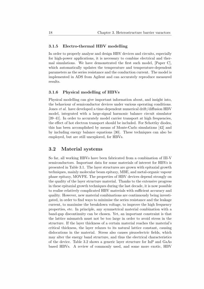
Today, planar geometries [43, 61] are used almost exclusively for HBVs.Planar HBVs are easy to mount in frequency multiplier circuits, mechan-ically stable and reliable, and suitable for integration with other compo-nents. The symmetric two-mesa structure generally employed also can-cels out any asymmetries in the epitaxial layer structure. The main draw-backs with planar diodes are the relatively complicated fabrication process,parasitic elements and the inherent problems associated with the effect ofself-heating [62, 63]. The planar HBV geometry employed at Chalmers isschematically shown in Figure 3.10. This planar diode geometry includestwo series-connected mesas, which means that an N -barrier material yieldsan N × 2-barrier device. The length and width of the air-bridge fingers andthe anode geometry are crucial parameters for the thermal properties [63].Figure 3.11 shows examples of planar HBVs fabricated at Chalmers.
3.3.4 Pillar geometries
A pillar diode topology for HBVs was suggested and fabricated at Chalmersby Alderman et al. [64]. Here, the substrate is removed and copper pil-lars are electroplated on each side of the mesa. This kind of device is verydifficult to fabricate, notably due to the thick resist layers needed for theelectroplating of the ∼20µm thick copper pillars. Due to various process-related problems all fabricated devices where short-circuited and thereforeno RF characterisation could be performed. However, the methods devel-
3.3. Practical HBVs 25
Finger/ohmic contact
Active layer
Contact/buffer layer
Substrate
Figure 3.10: Top (left) and cross-sectional (right) schematic views of the planarHBV geometry used at Chalmers.
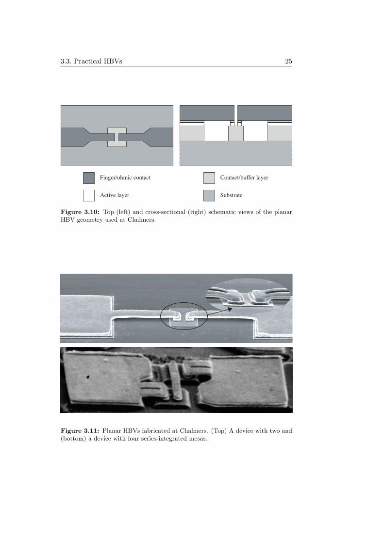
Figure 3.11: Planar HBVs fabricated at Chalmers. (Top) A device with two and(bottom) a device with four series-integrated mesas.

26 Chapter 3. Heterostructure barrier varactors
oped for using thick resist layers and for removing excessive semiconductormaterial during these experiments have been useful for process developmentof other device geometries. Figure 3.12 shows a pillar HBV soldered onto agold-on-quartz filter.
Figure 3.12: Pillar HBV soldered onto a gold-on-quartz filter.
3.3.5 Integrated devices
Integrated topologies are often desirable as they offer easier mounting, bettercontrol and improved performance compared to discretes. A design withmonolithically integrated low-pass filter, HBV diode and matching circuithas shown excellent performance [65]. Techniques, suitable for integration,for transferring HBVs to quartz substrates have been developed [66]. Thistransferring technique has resulted in HBVs monolithically integrated with alow-pass filter on a quartz substrate [67]. A possible, and indeed interesting,extension of these techniques could be to transfer HBVs to SiC or diamondsubstrates. Diamond and SiC have excellent thermal conductivities, whichmeans that such substrates could serve as very good heat-sinks for planarHBVs. A less expensive alternative would be to use Si.
3.3.6 High-power devices
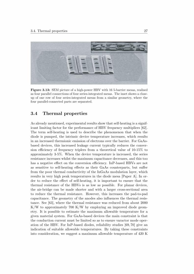
A multi-mesa HBV geometry designed to withstand very high power levelshas been developed at Chalmers, see Figure 3.13 [68]. Here the absorbedpower is distributed over a parallel connection of several series-connectedmesa configurations. Compared to the conventional planar diode geometry,the peak temperature in device is reduced drastically.
3.4. Thermal properties 27
Figure 3.13: SEM picture of a high-power HBV with 16 5-barrier mesas, realisedas four parallel connections of four series-integrated mesas. The inset shows a close-up of one row of four series-integrated mesas from a similar geometry, where thefour parallel-connected parts are separated.
3.4 Thermal properties
As already mentioned, experimental results show that self-heating is a signif-icant limiting factor for the performance of HBV frequency multipliers [62].The term self-heating is used to describe the phenomenon that when thediode is pumped, the intrinsic device temperature increases, which resultsin an increased thermionic emission of electrons over the barrier. For GaAs-based devices, this increased leakage current typically reduces the conver-sion efficiency of frequency triplers from a theoretical value of 10-15% toapproximately 3-5%. When the device temperature is increased, the seriesresistance increases whilst the maximum capacitance decreases, and this toohas a negative effect on the conversion efficiency. InP-based HBVs are notas sensitive to self-heating effects as their GaAs counterparts, but sufferfrom the poor thermal conductivity of the InGaAs modulation layer, whichresults in very high peak temperatures in the diode mesa [Paper A]. In or-der to reduce the effect of self-heating, it is important to ensure that thethermal resistance of the HBVs is as low as possible. For planar devices,the air-bridge can be made shorter and with a larger cross-sectional areato reduce the thermal resistance. However, this increases the pad-to-padcapacitance. The geometry of the anodes also influences the thermal resis-tance. See [63], where the thermal resistance was reduced from about 2000K/W to approximately 700 K/W by employing an improved diode geom-etry. It is possible to estimate the maximum allowable temperature for agiven material system. For GaAs-based devices the main constraint is thatthe conduction current must be limited so as to ensure varactor mode oper-ation of the HBV. For InP-based diodes, reliability studies [69, 70] give anindication of suitable allowable temperatures. By taking these constraintsinto consideration, we suggest a maximum allowable temperature of 420 K

28 Chapter 3. Heterostructure barrier varactors
for both GaAs and InP-based devices [Paper A]. This temperature can thenbe used as a design parameter when optimising the thermal properties ofHBVs, especially for high power applications [68].
3.4.1 Thermal estimations and models
3-D finite element (FEM) simulations are necessary to fully model and char-acterise the thermal properties of HBVs. Simple analytical expressions are,however, useful for initial estimations and comparisons between e. g. differ-ent material systems and device areas [Paper A]. The thermal resistance ofa semiconductor mesa surrounded by air is given by
Rth =L
κ ·A, (3.19)
where L is the length and A is the cross-sectional area of the mesa, and κis the thermal conductivity of the semiconductor material used. The one-dimensional steady state temperature profile throughout the mesa T (x) canbe calculated from the heat flow equation
∂2T (x)∂x2
= − Ptot
LAκ. (3.20)
Here a homogenously distributed heat source is assumed, and Ptot is thetotal power absorbed in the mesa. The solution to (3.20) and a discussionabout the results that can be obtained are given in [Paper A].
3.5 Design of HBV layer structures
An advantage with HBVs is that it is possible to tailor the devices fordifferent applications. For sub-millimetre wave applications, the main goalis to maximise the conversion efficiency for a given input frequency, inputpower level and multiplication factor. This is closely related to maximisingthe cut-off frequency, (2.3). At lower frequencies, higher input power levelsare available, and the HBV must also be optimised with respect to powerhandling capacity. Optimisation of the power handling capability involvesmaximising the breakdown voltage of the device. This section presents amethod for optimising the cut-off frequency, based on the work by Crowe etal. for Schottky diodes [26]. However, for terahertz operation, the currentsaturation effect must be taken into account [25]. The design goal is, then,to optimise the cut-off frequency with the current saturation effect as anoptimisation constraint. The optimum layer structure depends on the inputpower level and the diode geometry, since the series resistance depends onthe diode geometry and the number of barriers. For a given diode geometry,the design procedure is as follows.
3.5. Design of HBV layer structures 29
1. Choose material system, e.g. GaAs/AlxGa1−xAs on GaAs orInxGa1−xAs/AlyIn1−yAs on InP.
2. Estimate the number of barriers and the device area needed tohandle the input power [16].
3. Calculate the thickness of the modulation layers, lmax . Currentsaturation limits the maximum thickness to
lmax =vsat
4kfp(3.21)
where vsat is the saturated electron velocity, k is the ratio betweenvsat and the average electron speed during a half pump cycle [16] andfp is the pump frequency. For HBV triplers, k ≈ 2. The modulationlayers should be thick enough to accommodate the full depletion layerthickness at the maximum voltage during frequency multiplier oper-ation. Thicker layers will add extra series resistance, whilst thinnerlayers reduce the elastance modulation ratio.
4. Choose the doping concentration for the modulation layers. Inorder to minimise the series resistance, the modulation layers are usu-ally doped as heavily as possible, but not higher than that the mod-ulation layers can be fully depleted without exceeding the avalanchebreakdown voltage. A rough estimation of the breakdown voltage canbe derived from the well-known breakdown voltage expression for anabrupt PN-junction [71]
VBD = 60(
Eg
1.1
)3/2( ND
1016
)−3/4
(3.22)
where Eg is the band-gap at room temperature in eV and ND is thedoping concentration in cm−3. Equation (3.22) is accurate for manysemiconductors including GaAs, but does not seem be trustworthyfor InGaAs. We use modified versions of (3.22), fitted to breakdownvoltage measurements on InP-based HBV materials. The modulationlayer thickness l is obtained by inserting (3.22) into
l = wmax =
√2εdVBD
qNd(3.23)
where εd is the relative permittivity of the modulation layer materialand q is the elementary charge.
5. When a high frequency multiplier conversion efficiency is needed, thedynamic cut-off frequency has to be maximised. This involveschosing a layer structure and doping concentration that maximise theelastance swing and minimise the series resistance.

30 Chapter 3. Heterostructure barrier varactors
6. Choose the thickness of the barrier(s) to minimise the leakagecurrent [32] whilst still allowing for a high dynamic cut-off frequency.
7. Optimise the design with a harmonic balance simulator, using anappropriate voltage-charge relationship, (3.9), and a series resistanceestimated from material data and contact resistance measurements.
8. Check that the available input power can be absorbed without ex-ceeding the device breakdown voltage, optimum embedding impedancelevels are achievable, and the device temperature is below the maxi-mum allowable value. If not, iterate as appropriate by repeating thedesign procedure with a different number of barriers and/or a differentdevice area.
More detailed information on the design of HBVs can be found in [16] and[Paper B].
Chapter 4
HBV frequency multipliers
A two-terminal frequency multiplier uses a nonlinear device that generatesharmonics of the input frequency applied from a source. The nonlinear de-vice can be either a nonlinear resistor, varistor, or a nonlinear reactance,varactor. Varistor multipliers have a potentially large intrinsic bandwidthdue to the absence of stored reactive energy, but the conversion efficiencyis limited to 1/n2, where n is the order of multiplication [72, 73]. Varactormultipliers, on the other hand, have a theoretical conversion efficiency inthe ideal, loss-less case, of 100%, but have a narrow bandwidth and are verysensitive to the operating conditions. Due to the low available power levelsin the millimetre and sub-millimetre regions, varactors are used exclusivelyat these frequencies. However, practical varactors such as HBVs exhibitproperties that are a mixture of those of pure varistors and varactors, re-spectively. This section reviews basic design concepts for HBV multipliersand presents an overview of HBV multiplier cicuit topologies, performance,and measurement techniques.
4.1 Design of HBV multipliers
The design and analysis of frequency multipliers is an extensive topic. Thissection focuses on basic properties and device-related design issues, i. e.optimum impedance levels given certain device characteristics, or vice versa.Figure 4.1 shows the two possible basic forms for a single-HBV frequencymultiplier, namely with the diode mounted either in shunt or series withrespect to the input and output networks. The matching networks shouldbe designed to provide optimum embedding impedances to the diode atthe input and output frequency, respectively. Referring to Figure 4.1, inthe shunt connected topology, the input matching network should presentΓS = 1 (i. e. an open circuit) to the output frequency whilst the outputmatching network should provide ΓL = 1 at the fundamental frequency.For the series mounted case the opposite conditions must be fulfilled, i. e.
31

32 Chapter 4. HBV frequency multipliers
Inputmatchingnetwork(filter)
ΓSRG
PAVS fp
Outputmatchingnetwork(filter)
RL Pn; n × fp
ΓL
Inputmatchingnetwork(filter)
ΓSRG
PAVS fp
Outputmatchingnetwork(filter)
RL Pn; n × fp
ΓL
Figure 4.1: Schematic block representation of an nth-order frequency multipliercircuit with (top) shunt-mounted and (bottom) series-mounted diode.
ΓS = −1 for f = n×f0 and ΓL = −1 for f = f0, i. e. short circuits. For HBVmultipliers with n > 3 the matching networks must also provide appropriateidler circuits. An HBV quintupler (n = 5) for example needs an idler circuitfor the third harmonic, 3×f0, in order to maximise the conversion efficiencyto the fifth harmonic. There are two extreme cases for the realisation of theidler circuit, here represented by the idler impedance Z3, for a quintupler:
1. Zero current flowing at 3× f0, i. e. Z3 = ∞. The third harmonic willthus not cause any losses.
2. Maximise the current at 3× f0. This can be achieved by providing aninductance in resonance with the diode capacitance at 3 × f0. Thatis, Z3 = jX3, where Smin/3ωp < X3 < Smax/3ωp. This way the idlercurrent, in combination with the input signal, will increase the outputpower, but also introduce losses in the series resistance.
4.1.1 Optimum impedance levels
For frequency multipliers, optimum impedances means impedances that, ifpresented to the diode, maximise the conversion efficiency from f0 to n×f0.The optimum impedances are denoted e. g. ZS,opt and ZL,opt, respectively,and depend mutually on each other and on the input power level. However,generally, impedances are only defined for linear networks. Therefore, aquasi impedance Zn is defined at harmonic n of a periodic signal as
Zn =Vn
In, (4.1)
where Vn and In are the voltage and current, respectively, at harmonic n.In order to maximise the power transfer, the matching network impedance

4.1. Design of HBV multipliers 33
should be conjugate matched to device impedance. One analytical approachis to use the the cubic voltage-charge relation of (2.10). Then,the input andoutput impedances for optimum conversion efficiency can be approximatedby the following empirical expressions [74] :
Zin =(k1 − jk2)(Smax − Smin)− jSmin
ωp+ (k3 − jk4)Rs (4.2)
and
Zn =(k1 + jk2)(Smax − Smin) + jSmin
n · ωp+ (k3 + jk4)Rs, (4.3)
where ωp is the angular pump or input frequency. The constants kn aregiven in Table 4.1 for the cubic capacitance model. For fp/fc 1, k3 andk4 can be neglected.
Table 4.1: Coefficients for optimum tripler and quintupler impedances for thecubic model.
n k1 k2 k3 k4
3 Zin 0.046 0.21 0.78 0.25Z3 0.28 0.35 0.55 0.08
5 Zin 0.057 0.19 0.88 0.27Z3 0 0.35 0 0.29Z5 0.26 0.24 0.62 0.22
Load-pull simulations
Load-pull simulations are very useful for investigating impedance levels andtheir dependence on various parameters. To this end, we use Chalmers HBVmodel, (3.9), (3.10) or (3.12), and (3.14), implemented in the commercialsoftware Microwave Office. Harmonic balance simulations are used to deter-mine the optimum impedance levels. The result in the form of conversionloss contours from simulations of a 500 GHz HBV quintupler is shown inFigure 4.2. When Z1 is swept over the entire Smith chart, Z3 and Z5 arefixed at their respective optimum levels, and so forth. It is obvious that theinput matching is very crucial.
4.1.2 Noise in varactor multipliers
Being a mainly reactive device, a varactor generates very little noise. Ther-mal noise generated by the series resistance at all frequencies present is

34 Chapter 4. HBV frequency multipliers
Figure 4.2: Conversion loss contours versus (left) input and (right) idlerimpedance. The results are obtained from harmonic balance simulations of a 500GHz quintupler. The device assumed is a 2×3-barrier InP-based planar HBV withan area of 37 µm2. The minimum conversion loss is 5.1 dB and the contours cor-respond to an increase in conversion loss of 1 dB.
generally the dominating noise source in varactor multipliers [75]. As a con-sequence, in an application where the noise performance is important, it isnecessary to eliminate the current flowing at idler frequencies. The ther-mal noise generated in a bandwidth ∆f around a certain frequency can berepresented by the rms value of the noise voltage vn,rms:
vn,rms =√
4kTRs∆f (4.4)
where k is the Boltzmann constant and T is the device temperature. Afrequency multiplier also multiplies phase, the phase noise is degraded by n2,where n is the multiplication factor [13, 75]. No phase noise measurementshave yet been reported for HBVs.
4.2 HBV tripler and quintupler topologies
The vast majority of HBV multipliers this far have been frequency triplers.Today the focus is directed towards higher frequencies, and therefore theinterest for higher order multipliers, notably quintuplers, is increasing. Itis also possible to use HBVs for generating even harmonics by applying aDC bias that makes the energy band structure asymmetric. A few HBVfrequency doublers have been fabricated and tested, but nothing has beenpublished. The potential advantage of using HBVs rather than Schottkydiodes for frequency doubling is the higher power handling capacity offeredby a multi-barrier HBV. Triplers and quintuplers basically use the same kind

4.2. HBV tripler and quintupler topologies 35
of circuit topologies, the most commonly utilised of these are described inthis section.
4.2.1 Crossed waveguide multipliers
The most common multiplier configuration for millimetre and sub-millimetrewave applications is the crossed waveguide configuration. The circuit con-sists of a metal block with waveguides for the input and output signals, seeFigure 4.3. The widths of the waveguides correspond to the input frequencyfp and the output frequency n× fp, respectively. In the output waveguide,the input frequency is cut-off, which means that the waveguide acts as ahigh-pass filter, thus preventing power at fp from propagating to the outputof the multiplier. The pump power at fp is coupled to the output waveguidethrough a probe, which protrudes into the input waveguide. The probe isintegrated with a low-pass filter, which prevents power at n×fp leaking outto the input. Usually, the low-pass filter with the probe is made of gold-on-quartz in a high-low impedance configuration. In order to provide theHBV with suitable embedding impedances, it is common to include move-able shorts in the input and output waveguide sections, usually one E-planetuner and one backshort. The input tuners are shown in Figure 4.3. TheHBV, which is of a planar geometry in the circuit of Figure 4.3, is solderedwith one pad on to the end of the low-pass filter, and the other pad on tothe waveguide block. Waveguides exhibit low losses, although the moveableshorts introduce some losses in a multiplier circuit.
Low-pass filter
Input tuningbackshort
Input E-plane tuner
HBV diode
Output waveguide
Input waveguide
Figure 4.3: (Left) cross section of a crossed waveguide frequency multiplier and(right) photo of a 100-GHz HBV quintupler with two input tuners and one outputtuner.

36 Chapter 4. HBV frequency multipliers
4.2.2 Distributed multipliers
Another approach to the realisation of HBV frequency triplers is to usenonlinear transmission lines (NLTLs). NLTLs offer high bandwidths. Themain drawbacks are that the peak efficiency is lower than for single devicemultipliers, and that the mounting procedure is complex. To simplify theanalysis and design, it is preferable to use a linear transmission line, peri-odically loaded with nonlinear devices, rather than using a fully distributedNLTL. The first demonstration of an NLTL HBV tripler was performed byHollung et al. at Chalmers [76]. This tripler consists of a finline, periodicallyloaded with 15 HBVs, see Figure 4.4. The finline configuration is possibleto use, as HBVs do not need any DC bias. Propagation of the incidentwave through the nonlinear transmission line generates the third harmonic,which is radiated into free space from a tapered slot antenna at the output.Recently, a broadband integrated HBV tripler using a nonlinear transmis-
HBVs
Finline
Tapered slot antenna
WR-22 waveguideWaveguide input:Q-band
Radiated output:F-band
Quartz substrate
Figure 4.4: A distributed HBV frequency tripler [76].
sion line topology with six HBVs was presented [77]. Here, HBVs and finlinetransitions are integrated on a low-loss membrane to reduce parasitics andenable output frequencies up to 600 GHz.
4.2.3 Waveguide-integrated microstrip multipliers
At Chalmers we have developed a new HBV multiplier topology where theHBV is embedded in a microstrip environment together with parts of thematching network, see Olsen et al., [78]. The topology is suitable for bothtriplers [Paper F] and quintuplers [Paper E]. The circuit is mounted in arectangular waveguide and e. g. antipodal finline tapers can be used astransitions between the waveguide and the microstrip circuit. A triplerversion of this circuit topology is shown in Figure 4.5. Figure 4.6 shows aphoto of a 100-GHz waveguide-integrated microstrip quintupler [Paper E].

4.3. Frequency multiplier measurements 37
Q-band WG to microstrip transition Microstrip section F-band microstrip to WG transition
Top planeBottom plane
HBV
Figure 4.5: A waveguide-integrated microstrip HBV tripler with antipodal finlinetransitions and microstrip embedding circuit.
Figure 4.6: Detail of a 100-GHz HBV waveguide-integrated microstrip quintupler.The gold-on-quartz circuit is mounted in a channel between the input (left) andoutput (right) waveguides [Paper E].
4.2.4 Quasi-optical multipliers
Quasi-optical circuits are well suited for high-frequency applications, espe-cially the upper sub-millimetre wave region, where the losses in waveguidecircuits are higher and affect the performance noticeably. Decreasing dimen-sions also complicate the machining of waveguide circuits at these frequen-cies. Figure 4.7 shows a quasi-optical HBV frequency tripler, where two slotantennas loaded with HBVs are located at the focal plane of a dielectriclens [79].
4.3 Frequency multiplier measurements
4.3.1 Measurements on waveguide multipliers
Hitherto, most HBV circuits have been triplers designed to operate at inputfrequencies in the W-band, 75-110 GHz. The two main constraints whenchoosing frequency bands for multiplier design, in terms of characterisationpossibilities, are (i) the availability of fundamental power sources and (ii)the availability of power measurement devices. At W-band, Gunn oscil-lators and backward-wave oscillators (BWOs) can produce power levels ofabout 100 mW, or 20 dBm. A typical measurement set-up is schematicallyshown in Figure 4.8, whilst Figure 4.9 shows a photo of such a set-up forHBV waveguide quintupler measurements. Figure 4.10 shows results frommeasurements on a typical HBV tripler.

38 Chapter 4. HBV frequency multipliers
Slot antennas,HBV diodes
Quartz substrate
High-pass filter
Alumina spacer
Alumina lens
f0 = 47 GHz
3f0 = 141 GHz
Figure 4.7: A quasi-optical HBV frequency tripler [79].
Signal source
DUTPowermeter
Powermeterfp n × fp
Figure 4.8: Schematical representation of a typical measurement set-up for waveg-uide multiplier measurements.
Figure 4.9: Photo of a measurement set-up for a waveguide circuit, showing powermeters, signal synthesiser with an amplifier, waveguide block with moveable tunersand directional coupler.

4.3. Frequency multiplier measurements 39
0
0.5
1
1.5
41 41.5 42 42.5 43 43.5 44
Pin = 10 dBmPin = 13 dBmPin = 16 dBm
Pump frequency [GHz]
Out
put p
ower
[dB
m]
Figure 4.10: Output power versus pump frequency for an F-band HBV frequencytripler for three different levels of input power.

40 Chapter 4. HBV frequency multipliers
4.3.2 Cooled measurements
Results from cooled measurements are useful for evaluating the thermalproperties of HBV device geometries. The performance obtained from mea-surements on HBV multipliers at room temperature can be compared to theresults obtained at cooled temperatures. Well-designed diodes should showless difference in efficiencies at different temperatures, cf [35, 62]. Cooledmeasurements are performed in a vacuum environment inside a cryostat. Aproblem, then, is that when the circuit is mounted inside the cryostat, it isnot possible to perform any tuning of the circuit. This problem can be solvedby using a computer-controlled system, where the computer performs theimpedance matching of the circuit with stepper motors. The stepper mo-tors are connected to drive shafts, which penetrate the walls of the cryostatthrough vacuum feed-throughs, and are connected to moveable tuners onthe circuit [80]. Figure 4.11 (left) shows a photograph of such a cryostatwith the top lid removed and an HBV tripler mounted on the 20 K stage.The computer-controlled system can also be used for circuit characterisationat room temperature. An example is shown in Figure 4.11 (right). A cooled
Backshort tuner position [µm] E-plane tu
ner positi
on [µm]
Out
put p
ower
[µ
W]
Figure 4.11: (Left) photo of a cryostat equipped with stepper motors, allowingfor computer-controlled impedance matching and measurements. (Right) outputpower versus position of the output tuners from an HBV tripler, measured with thecomputer-controlled system [80].
measurement performed in the cryostat of Figure 4.11 is shown in Figure4.12.
4.4 HBV multiplier performance
Table 4.2 summarises the state-of-the-art for HBV triplers and quintuplersat various frequencies. The results presented are also visualised in Figure4.13.

4.4. HBV multiplier performance 41
0
200
400
600
800
1000
0 50 100 150 200 250 300
Out
put p
ower
[µ
W]
Tripler mount temperature [K]
fp: 85 GHz
Area: 57 µm2
Pava: 55mW
Figure 4.12: Measured output power versus mount temperature for an HBVtripler with a 2×2-barrier GaAs-based diode [62].
0,01
0,1
1
10
100
10 100 1000
Output frequency [GHz]
Out
put p
ower
[mW
]
Figure 4.13: Output power versus output frequency for the HBV multiplierssummarised in Table 4.2.

42 Chapter 4. HBV frequency multipliers
Table 4.2: HBV multiplier performance.
f η Pout N Sub. Ref. Comment[GHz] [%] [mW]
3 × 13.5 7.6 12 3 InP [81]3 × 31 10 91 10 InP [48]3 × 33 0.7 1250 3 GaAs [82] Quasi-optical
3 × 43.5 7 10 4 GaAs [76] NLTL3 × 47 8 11.5 4 GaAs [79] Quasi-optical3 × 62 2 0.8 1 GaAs [83]3 × 70 13.5 10 1 GaAs [65]3 × 72 5.4 5 4 InP [20]3 × 74 7.9 7.1 3 Cu [35]3 × 82 4.8 4 4 GaAs [63]
3 × 82.5 12 9 4 InP [84]3 × 84 2.5 2 4 GaAs [43]3 × 89 5.6 4.3 3 Cu [19]3 × 96 6 6 6 Quartz [67]3 × 150 0.05 0.08 2 Au [23]3 × 150 1.5 1 4 GaAs [85]
5 × 19.7 11.4 4.6 4 InP [Paper D]5 × 20.5 4.9 1.0 4 GaAs [Paper E]5 × 34 0.78 0.03 1 InP [86]
5 × 42.5 5.2 5.2 4 InP [87]
Chapter 5
Summary of appendedpapers
Paper A presents an analytical model for the temperature profile through-out an HBV.
Paper B deals with device-level design of high frequency HBV multipliers,exemplified by a 500 GHz quintupler design.
Paper C presents an electro-thermal HBV model for harmonic balance anal-ysis including self-heating effects.
Paper D presents world-record results for HBV quintuplers.
Paper E describes a 100 GHz HBV quintupler.
Paper F presents an F-band HBV tripler.
Paper G describes the fabrication of HBVs on copper substrates.
43

44 Chapter 5. Summary of appended papers
References
[1] P. H. Siegel, “Terahertz technology in biology and medicine,” IEEETransactions on Microwave Theory and Techniques, vol. 52, no. 10, pp.2438–2447, 2004.
[2] R. Kohler, A. Tredicucci, F. Beltram, H. E. Beere, E. H. Linfield,A. G. Davies, D. A. Ritchie, R. C. Iotti, and F. Rossi, “Terahertzsemiconductor-heterostructure laser,” Nature, vol. 417, pp. 156–159,2002.
[3] B. S. Williams, H. Callebaut, S. Kumar, Q. Hu, and J. L. Reno, “3.4-THz quantum cascade laser based on longitudinal-optical-phonon scat-tering for depopulation,” Applied Physics Letters, vol. 82, no. 7, pp.1015–1017, 2003.
[4] B. S. Williams, S. Kumar, H. Callebaut, Q. Hu, and J. L. Reno, “Tera-hertz quantum-cascade laser at λ ≈100µm using metal waveguide formode confinement,” Applied Physics Letters, vol. 83, no. 11, pp. 2124–2126, 2003.
[5] S. C. Lee and A. Wacker, “Theoretical analysis of spectral gain in aterahertz quantum-cascade laser: Prospects for gain at 1 THz,” AppliedPhysics Letters, vol. 83, no. 13, pp. 2506–2508, 2003.
[6] E. Peytavit, S. Arscott, D. Lippens, G. Mouret, S. Matton, P. Masselin,R. Bocquet, J. F. Lampin, L. Desplanque, and F. Mollot, “Terahertzfrequency difference from vertically integrated low-temperature-grownGaAs photodetector,” Applied Physics Letters, vol. 81, no. 7, pp. 1174–1176, 2002.
[7] H. Ito, T. Nagatsuma, A. Hirata, T. Minotani, A. Sasaki, Y. Hirota,and T. Ishibashi, “High-power photonic millimetre wave generation at100 GHz using matching-circuit-integrated uni-travelling-carrier photo-diodes,” IEE Proceedings Optoelectronics, vol. 150, no. 2, pp. 138–142,2003.
45

46 REFERENCES
[8] T. Crowe, R. Mattauch, H. Roser, W. Bishop, W. Peatman, and X. Liu,“GaAs Schottky diodes for THz mixing applications,” Proceedings ofthe IEEE, vol. 80, no. 11, pp. 1827–1841, 1992.
[9] N. R. Erickson, R. M. Grosslein, J. Wielgus, and V. Fath, “A 1650-1900 GHz tunable source,” in Proceedings of the 14th InternationalSymposium on Space Terahertz Technology, 2003, pp. 64–72.
[10] E. L. Kollberg and A. Rydberg, “Quantum-barrier-varactor diodes forhigh-efficiency millimetre-wave multipliers,” Electronics Letters, vol. 25,no. 25, pp. 1696–1698, 1989.
[11] P. Penfield and R. P. Rafuse, Varactor Applications. Cambridge:M.I.T. Press, 1962.
[12] J. Stake, The RF and microwave handbook. CRC Press LLC, 2001,ch. Varactors.
[13] M. T. Faber, J. Chramiec, and M. E. Adamski, Microwave andMillimeter-Wave Diode Frequency Multipliers. Artech House, 1995.
[14] J. W. Manley and H. E. Rowe, “Some general properties of nonlinearelements,” Institute of Radio Engineers - Proceedings, vol. 44, no. 7,pp. 904–913, 1956.
[15] L. Dillner, J. Stake, and E. L. Kollberg, “Analysis of symmetric varac-tor frequency multipliers,” Microwave and Optical Technology Letters,vol. 15, no. 1, pp. 26–29, 1997.
[16] J. Stake, S. H. Jones, L. Dillner, S. Hollung, and E. L. Koll-berg, “Heterostructure-barrier-varactor design,” IEEE Transactions onMicrowave Theory and Techniques, vol. 48, no. 4, pp. 677 – 682, 2000.
[17] K. Krishnamurthi and R. G. Harrison, “Analysis of symmetric-varactorfrequency triplers,” in IEEE MTT-S International Microwave Sympo-sium Digest, 1993, pp. 649–652.
[18] C. H. Tang, “An exact analysis of varactor frequency multipliers,” IEEETransactions on Microwave Theory and Techniques, vol. 14, no. 4, pp.210–212, 1966.
[19] L. Dillner, “Heterostructure barrier varactors for high efficiency fre-quency multipliers,” Ph.D. dissertation, Chalmers University of Tech-nology, 2000.
[20] X. Melique, C. Mann, P. Mounaix, J. Thornton, O. Vanbesien, F. Mol-lot, and D. Lippens, “5-mW and 5% efficiency 216-GHz InP-basedheterostructure barrier varactor tripler,” IEEE Microwave and GuidedWave Letters, vol. 8, no. 11, pp. 384–386, 1998.

REFERENCES 47
[21] X. Melique, A. Maestrini, R. Farre, P. Mounaix, M. Favreau,O. Vanbesien, J. M. Goutoule, F. Mollot, G. Beaudin, T. Nahri, andD. Lippens, “Fabrication and performance of InP-based heterostructurebarrier varactors in a 250 GHz waveguide tripler,” IEEE Transactionson Microwave Theory and Techniques, vol. 48, no. 6, pp. 1000–1006,2000.
[22] L. Dillner, S. Hollung, M. Ingvarson, E. Kollberg, W. Strupinski,C. Mann, and J. Stake, “High efficiency HBV multipliers for millimeterwave generation,” in Proceedings of the 13th International Conferenceon Microwaves, Radar and Wireless Communications, 2000, pp. 47–54.
[23] M. Saglam, B. Schumann, V. Mullerwiebus, A. Megej, U. Auer,M. Rodriguez-Girones, R. Judaschke, E. Tegude, and H. Hartnagel,“450 GHz millimetre-wave signal from frequency tripler with hetero-structure barrier varactors on gold substrate,” Electronics Letters,vol. 38, no. 13, pp. 657–658, 2002.
[24] Y. Fu, M. Mamor, M. Willander, S. Bengtsson, and L. Dillner, “n-Si/SiO2/Si heterostructure barrier varactor diode design,” AppliedPhysics Letters, vol. 77, no. 1, pp. 103–105, 2000.
[25] E. L. Kolberg, T. J. Tolmunen, M. A. Frerking, and J. R. East, “Cur-rent saturation in submillimeter-wave varactors,” IEEE Transactionson Microwave Theory and Techniques, vol. 40, no. 5, pp. 831 – 838,1992.
[26] T. W. Crowe, T. C. Grein, R. Zimmermann, and P. Zimmermann,“Progress toward solid-state local oscillators at 1 THz,” IEEE Micro-wave and Guided Wave Letters, vol. 6, no. 5, pp. 207–208, 1996.
[27] J. Stake and H. Gronqvist, “An on-wafer method for C-V character-isation of heterostructure diodes,” Microwave and Optical TechnologyLetters, vol. 9, no. 2, pp. 63–66, 1995.
[28] J. Stake, L. Dillner, S. H. Jones, E. L. Kollberg, and C. M. Mann, “De-sign of 100-900 GHz AlGaAs/GaAs planar heterostructure barrier var-actor frequency triplers,” in Proceedings of the 9th International Sym-posium on Space Terahertz Technology, 1998, pp. 359–366.
[29] L. Dillner, J. Stake, and E. L. Kollberg, “Modeling of the hetero-structure barrier varactor diode,” in Proceedings of the 1997 Interna-tional Semiconductor Device Research Symposium, 1997, pp. 179–182.
[30] H. Hjelmgren, “Numerical modelling of hot electron transport inSchottky-diodes and heterojunction structures,” Ph.D. dissertation,Chalmers University of Technology, 1991.

48 REFERENCES
[31] J. R. Jones, S. H. Jones, G. B. Tait, and M. F. Zybura, “Hetero-structure barrier varactor simulation using an integrated hydrodynamicdevice/harmonic-balance circuit analysis technique,” IEEE Microwaveand Guided Wave Letters, vol. 4, no. 12, pp. 411–413, 1994.
[32] Y. Fu, J. Stake, L. Dillner, M. Willander, and E. L. Kollberg, “Al-GaAs/GaAs and InAlAs/InGaAs heterostructure barrier varactors,”Journal of Applied Physics, vol. 82, no. 11, pp. 5568–5572, 1997.
[33] E. Lheurette, P. Mounaix, P. Salzenstein, F. Mollot, and D. Lippens,“High performance InP-based heterostructure barrier varactors in singleand stack configuration,” Electronics Letters, vol. 32, no. 15, pp. 1417–1418, 1996.
[34] Y. Fu, J. Stake, L. Dillner, M. Willander, and E. L. Kollberg, “Carrierconduction in a heterostructure barrier varactor induced by an ac-bias,”Superlattices and Microstructures, vol. 28, no. 2, pp. 135–141, 2000.
[35] L. Dillner, W. Strupinski, S. Hollung, C. Mann, J. Stake, M. Beards-ley, and E. Kollberg, “Frequency multiplier measurements on hetero-structure barrier varactors on a copper substrate,” IEEE Electron De-vice Letters, vol. 21, no. 5, pp. 206 – 208, 2000.
[36] J. Stake, L. Dillner, and M. Ingvarson, “Fabrication and characterisa-tion of heterostructure barrier varactor diodes,” Chalmers Universityof Technology, Tech. Rep. 29, 1996.
[37] L. E. Dickens, “Spreading resistance as a function of frequency,” IEEETransactions on Microwave Theory and Techniques, vol. 15, no. 2, pp.101–109, 1967.
[38] M. Sotoodeh, A. H. Khalid, and A. A. Rezazadeh, “Empirical low-fieldmobility model for III–V compounds applicable in device simulationcodes,” Journal of Applied Physics, vol. 87, no. 6, pp. 2890–2900, 2000.
[39] J. R. Jones, S. H. Jones, and G. B. Tait, “Self-consistent physics-basednumerical device/harmonic-balance circuit analysis of heterostructurebarrier varactors including thermal effects,” in Proceedings of the 6th In-ternational Symposium on Space Terahertz Technology, 1995, pp. 423–441.
[40] J. R. Jones, G. Tait, S. Jones, and D. Katzer, “DC and large-signaltime-dependent electron transport in heterostructure devices: an inves-tigation of the heterostructure barrier varactor,” IEEE Transactions onElectron Devices, vol. 42, no. 8, pp. 1393–1403, 1995.

REFERENCES 49
[41] J. Stake, S. H. Jones, J. R. Jones, and L. Dillner, “Analysis of car-rier transport in a heterostructure barrier varactor diode tripler,” inProceedings of the 1997 International Semiconductor Device ResearchSymposium, 1997, pp. 183–186.
[42] R. E. Lipsey, S. H. Jones, J. R. Jones, T. W. Crowe, L. F. Horvath,U. V. Bhapkar, and R. J. Mattauch, “Monte Carlo harmonic-balanceand drift-diffusion harmonic-balance analyses of 100-600 GHz Schottkybarrier varactor frequency multipliers,” IEEE Transactions on ElectronDevices, vol. 44, no. 11, pp. 1843–1850, 1997.
[43] J. R. Jones, W. L. Bishop, S. H. Jones, and G. B. Tait, “Planar multi-barrier 80/240-GHz heterostructure barrier varactor triplers,” IEEETransactions on microwave theory and techniques, vol. 45, no. 4, pp.512–518, 1997.
[44] K. Krishnamurthi, S. M. Nilsen, and R. G. Harrison, “GaAs single-barrier varactors for millimeter-wave triplers: guidelines for enhancedperformance,” IEEE Transactions on Microwave Theory and Tech-niques, vol. 42, no. 12, pp. 2512 – 2516, 1994.
[45] J. R. Jones, S. H. Jones, and G. B. Tait, “GaAs/InGaAs/AlGaAsheterostructure barrier varactors for frequency tripling,” in Proceed-ings of the 5th International Symposium on Space Terahertz Technol-ogy, 1994, pp. 497–513.
[46] V. Duez, X. Melique, O. Vanbesien, P. Mounaix, F. Mollot, andD. Lippens, “High capacitance ratio with GaAs/InGaAs/AlAs hetero-structure quantum well-barrier varactors,” Electronics Letters, vol. 34,no. 19, pp. 1860 – 1861, 1998.
[47] V. K. Reddy and D. P. Neikirk, “High breakdown voltage AlAs/InGaAsquantum barrier varactor diodes,” Electronics Letters, vol. 29, no. 5, pp.464 – 466, 1993.
[48] A. Rahal, R. G. Bosisio, C. Rogers, J. Ovey, M. Sawan, and M. Mis-sous, “A W-band medium power multi-stack quantum barrier varactorfrequency tripler,” IEEE Microwave and Guided Wave Letters, vol. 5,no. 11, pp. 368–370, 1995.
[49] W. Strupinski, L. Dillner, J. Sass, K. Kosiel, J. Stake, M. Ingvarson, andR. Jakiela, “MOVPE strain layers - growth and application,” Journalof Crystal Growth, vol. 221, pp. 20–25, 2000.
[50] M. Ingvarson, L. Dillner, W. Strupinski, and J. Stake, “Design of ma-terial structures for heterostructure barrier varactors,” in Presented atthe 19th Nordic Semiconductor Meeting, 2001.

50 REFERENCES
[51] M. Ingvarson, A. Ø. Olsen, B. Alderman, and J. Stake, “Hetero-structure barrier varactor frequency multipliers: materials, devices andcircuits,” in Proceedings of GHz 2001, Lund, 2001.
[52] E. Lheurette, X. Melique, P. Mounaix, F. Mollot, O. Vanbesien, andD. Lippens, “Capacitance engineering for InP-based heterostructurebarrier varactor,” IEEE Electron Device Letters, vol. 19, no. 9, pp.338–340, 1998.
[53] J. Stake, L. Dillner, and E. Kollberg, “Investigation of an InAs basedheterostructure barrier varactor,” in Proceedings of GHz 1995, 1995,pp. PS33–34.
[54] K. Inoue, J. C. Harmand, and T. Matsuno, “High-qualityInxGa1−xAs/InAlAs modulation doped heterostructures grown lattice-mismatched on GaAs-substrates,” Journal of Crystal Growth, vol. 111,no. 1-4, pp. 313–317, 1991.
[55] T. Mishima, K. Higuchi, M. Mori, and M. Kudo, “High gm
In0.5Al0.5As/In0.5Ga0.5As high electron mobility transistors grownlattice-mismatched on GaAs substrates,” Journal of Crystal Growth,vol. 150, pp. 1230–1235, 1995.
[56] M. Saglam, K. Mutamba, A. Megej, C. Sydlo, and H. L. Hartnagel, “In-fluence of polarization charges in Al0.4Ga0.6N/GaN barrier varactors,”Applied Physics Letters, vol. 82, no. 2, pp. 227–229, 2003.
[57] J. M. DiDomenico, D. A. Johnson, and R. H. Pantell, “Ferroelectricharmonic generator and the large-signal microwave characteristics of aferroelectric ceramic,” Journal of Applied Physics, vol. 33, no. 5, pp.1697–1706, 1962.
[58] P. Rundqvist, “Perovskite oxides for parallel plate ferroelectric varac-tors,” Chalmers University of Technology, Tech. Rep. 488L, 2004.
[59] R. Williams, Modern GaAs processing methods, 2nd ed. Artech House,1990.
[60] L. Dillner, J. Stake, and E. L. Kollberg, “Heterostructure barrier var-actors on copper substrate,” Electronics Letters, vol. 339 - 341, no. 4,pp. 339–341, 1999.
[61] J. Stake, “Planar heterostructure barrier varactor diodes for millimetrewave applications,” Ph.D. dissertation, Chalmers University of Tech-nology, 1999.
[62] J. Stake, L. Dillner, S. H. Jones, C. M. Mann, J. Thornton, J. R.Jones, W. L. Bishop, and E. L. Kollberg, “Effects of self-heating on

REFERENCES 51
planar heterostructure barrier varactor diodes,” IEEE Transactions onElectron Devices, vol. 45, no. 11, pp. 2298–2303, 1998.
[63] J. Stake, C. Mann, L. Dillner, M. Ingvarson, S. H. Jones, S. Hollung,H. Mohamed, B. Alderman, M. Chamberlain, and E. Kollberg, “Im-proved diode geometry for planar heterostructure barrier varactors,” inProceedings of the 10th International Symposium on Space TerahertzTechnology, Charlottesville, 1999, pp. 485–491.
[64] B. Alderman, J. Stake, L. Dillner, D. P. Steenson, M. Ingvarson,E. Kollberg, C. Mann, and J. Chamberlain, “A new pillar geometry forheterostructure barrier varactor diodes,” in Proceedings of the 12th In-ternational Symposium on Space Terahertz Technology, 2001, pp. 330–339.
[65] R. Meola, J. Freyer, and M. Claassen, “Improved frequency tripler withintegrated single-barrier varactor,” Electronics Letters, vol. 36, no. 99,pp. 803–804, 2000.
[66] S. Arscott, P. Mounaix, and D. Lippens, “Transferred InP-based HBVson glass substrate,” Electronics Letters, vol. 35, no. 17, pp. 1493 – 1494,1999.
[67] T. David, S. Arscott, J. M. Munier, T. Akalin, P. Mounaix, G. Beaudin,and D. Lippens, “Monolithic integrated circuits incorporating InP-based heterostructure barrier varactors,” IEEE Microwave and Wire-less Component Letters, vol. 12, no. 8, pp. 281 – 283, 2002.
[68] A. Emadi, J. Vukusic, M. Ingvarson, T. Bryllert, Ø. Olsen, E. Kollberg,and J. Stake, “High power HBV multipliers for F- and G- band applica-tions,” in Proceedings of the Joint 29th IRMMW2004 / 12th THz2004,2004, pp. 319–320.
[69] M. Tutt, G. I. Ng, D. Pavlidis, and J. Mansfield, “Reliability issuesof InAlAs/InGaAs high-electron mobility transistors,” in Proceedingsof the 3rd International Conference on Indium Phosphide and RelatedMaterials, 1991, pp. 349–352.
[70] R. Kamoua and H. Eisele, “Theoretical and experimental comparisonof optimized doping profiles for high-performance InP Gunn devices at220-500 GHz,” in MTT-S International Microwave Symposium Digest,2003, pp. 907–910.
[71] S. M. Sze, Physics of Semiconductor Devices, 2nd ed. John Wiley &Sons, 1981.
[72] C. H. Page, “Harmonic generation with ideal rectifiers,” Institute ofRadio Engineers - Proceedings, vol. 46, pp. 1738–1740, 1958.

52 REFERENCES
[73] R. H. Pantell, “General power relationships for positive and negativenonlinear resistive elements,” Institute of Radio Engineers - Proceed-ings, vol. 46, no. 12, pp. 1910–1913, 1958.
[74] E. L. Kollberg, J. Stake, and L. Dillner, “Heterostructure barrier varac-tors at submillimetre waves,” Philosophical Transactions of the RoyalSociety London A, vol. 354, no. 1717, pp. 2383–2398, 1996.
[75] S. A. Maas, Nonlinear Microwave and RF Circuits, 2nd ed. ArtechHouse, 2003.
[76] S. Hollung, J. Stake, L. Dillner, M. Ingvarson, and E. Kollberg, “Adistributed heterostructure barrier varactor frequency tripler,” IEEEMicrowave and Guided Wave Letters, vol. 48, no. 4, pp. 24–26, 2000.
[77] W. H. Chow, D. P. Steenson, T. T. Piotrowski, A. Piotrowska, andK. Golaszewska, “An integrated micromachined waveguide frequencytripler for nonlinear wave propagation,” in Proceedings of the IEEEAntennas and Propagation Society Symposium, 2004, pp. 1563–1566.
[78] A. Ø. Olsen, J. Stake, M. Ingvarson, D. P. Steenson, and S. Iezekiel,“A new waveguide integrated microstrip heterostructure barrier var-actor (hbv) frequency tripler,” in Proceedings of the 9th InternationalConference on Terahertz Electronics, Charlottesville, 2001.
[79] S. Hollung, J. Stake, L. Dillner, and E. Kollberg, “A 141 GHz quasi-optical HBV diode frequency tripler,” in Proceedings of the 10th Inter-national Symposium on Space Terahertz Technology, 1999, pp. 492–500.
[80] M. Ingvarson, L. Dillner, S. Hollung, E. Kollberg, C. Mann, andJ. Stake, “Computer controlled measurements on millimetre and sub-millimetre wave varactor multipliers,” in Proceedings of GHz 2000,2000, pp. 297–300.
[81] K. Krishnamurthi, E. Boch, and R. G. Harrison, “A Ka-band planartripler based on a stacked symmetric InP heterostructure-barrier var-actor,” in IEEE MTT-S International Microwave Symposium Digest,1995, pp. 549–552.
[82] H. X. L. Liu, L. B. Sjogren, C. W. Domier, J. N. C. Luhmann, D. L.Sivco, and A. Y. Cho, “Monolithic quasi-optical frequency tripler arraywith 5-W output power at 99 GHz,” IEEE Electron Device Letters,vol. 14, no. 7, pp. 329–331, 1993.
[83] D. Choudhury, M. A. Frerking, and P. D. Batelaan, “A 200 GHz triplerusing a single barrier varactor,” IEEE Transactions on Microwave The-ory and Techniques, vol. 41, no. 4, 1993.

REFERENCES 53
[84] X. Melique, A. Maestrini, E. Lheurette, P. Mounaix, M. Favreau,O. Vanbesien, J. M. Goutoule, G. Beaudin, T. Nahri, and D. Lippens,“12% efficiency and 9.5 dBm output power from InP-based hetero-structure barrier varactor triplers at 250 GHz,” in IEEE MTT-S In-ternational Microwave Symposium Digest, 1999.
[85] M. Saglam, B. Schumann, K. Duwe, C. Domoto, A. Megej,M. Rodriguez-Girones, J. Muller, R. Judaschke, and H. Hartnagel,“High-performance 450-GHz GaAs-based heterostructure barrier var-actor tripler,” IEEE Electron Device Letters, vol. 24, no. 3, pp. 138 –140, 2003.
[86] A. V. Raisanen, T. J. Tolmunen, M. Natzic, M. A. Frerking, E. Brown,H. Gronqvist, and S. M. Nilsen, “A single barrier varactor quintupler at170 GHz,” IEEE Transactions on Microwave Theory and Techniques,no. 3, pp. 685–688, 1995.
[87] Q. Xiao, Y. Duan, J. L. Hesler, T. W. Crowe, and R. M. Weikle II,“A 5-mW and 5% efficiency 210 GHz InP-based heterostructure bar-rier varactor quintupler,” IEEE Microwave and Wireless ComponentLetters, vol. 14, no. 4, pp. 159–161, 2004.