Embed Size (px)
Citation preview

Modeling Photonic Links in Verilog-A
by
Ekaterina Kononov
B.S. E.E., MIT (2012)
Submitted to the Department of Electrical Engineering and ComputerScience
in partial fulfillment of the requirements for the degree of
Master of Engineering in Computer Science and Engineering
at the
MASSACHUSETTS INSTITUTE OF TECHNOLOGY
June 2013
® 2013 Ekaterina Kononov. All rights reserved.
The author hereby grants to MIT permission to reproduce and todistribute publicly paper and electronic copies of this thesis document
in whole or in part in any medium now known or hereafter created.
Author....................................Department of Electrical Engineering and Computer Science
May 24, 2013
Certified by ...........
7/ Vladimir StojanovicAssociate Professor
Thesis Supervisor
Accepted by .............................. ..... ........Prof. Dennis M. Freeman
Chairman, Masters of Engineering Thesis Committee

2

Modeling Photonic Links in Verilog-A
by
Ekaterina Kononov
Submitted to the Department of Electrical Engineering and Computer Scienceon May 24, 2013, in partial fulfillment of the
requirements for the degree ofMaster of Engineering in Computer Science and Engineering
Abstract
Integrated photonic links are a promising emerging technology that can relieve the in-
terconnect bottleneck in core-to-core and core-to-memory communications of modern
processors. Developing and optimizing photonic link systems requires simulation of
integrated photonic devices side-by-side with electronic devices at the device, circuit,and system level. In previous efforts to simulate photonic links, the optical and the
electrical signals were treated in separate simulators, which resulted in some loss of
accuracy. In this thesis, a library of photonic device models is developed in Verilog-A
for use in seamless simulation of opto-electronic circuits in Cadence.
Thesis Supervisor: Vladimir Stojanovic
Title: Associate Professor
3

4

Acknowledgments
Everyone in ISG, especially everyone on the photonics project. In particular, Mike
who taught me the basics and sparked my interest in the beginning, Jonathan who
made invaluable contibutions to the project with his Verilog expertise. Special thanks
to Cheri for her patience in each of the many times she explained to me how a ring
modulator works. Most importantly, Vladimir under whose supervision I stayed on-
task and on-schedule.
5

6

Contents
1 Introduction 13
1.1 The Need for Models . . . . . . . . . . . . . . . . . . . . . . . . . . . 14
2 Background 15
2.1 Photonic Link Overview . . . . . . . ... . . . . . . . . . . . . . . . . 15
2.1.1 An Example Photonic Link . . . . . . . . . . . . . . . . . . . 15
2.1.2 Photonic Link Components . . . . . . . . . . . . . . . . . . . 16
2.2 Verilog-A . . . . . . . . . . . . . . . . . . . . . . . . . . . . . . . . . 20
3 Previous Work 23
3.1 OptiSPICE, a Photonics Simulator . . . . . . . . . . . . . . . . . . . 23
3.2 Magnitude and Phase. . . . . . . . . . . . . . . . . . . . . . . . . . . 24
3.3 Optical Devices . . . . . . . . . . . . . . . . . . . . . . . . . . . . . . 25
4 Models 27
4.1 Continuous-Wave Laser Source . . . . . . . . . . . . . . . . . . . . . 27
4.1.1 PolToCart and CartToPol . . . . . . . . . . . . . . . . . . . . 28
4.2 Waveguide . . . . . . . . . . . . . . . . . . . . . . . . . . . . . . . . . 29
4.3 Passive Ring Resonator . . . . . . . . . . . . . . . . . . . . . . . . . . 30
4.3.1 Cross-Coupler . . . . . . . . . . . . . . . . . . . . . . . . . . . 31
4.3.2 Thermal Tuning of Ring Resonators . . . . . . . . . . . . . . . 31
4.4 Ring Modulator . . . . . . . . . . . . . . . . . . . . . . . . . . . . . . 32
4.4.1 Phase Shifter . . . . . . . . . . . . . . . . . . . . . . . . . . . 33
7

4.5 Photodetector . . . . . . .
4.6 Optical Combiner . . . . .
5 Simulation Results
5.1 Verification of Individual C
5.1.1 Laser . . . . . . . .
5.1.2 Combiner . . . . .
5.1.3 Waveguide . . . . .
5.1.4 Modulator . . . . .
5.1.5 Photodetector . . .
5.2 Full Link Simulation . . .
5.2.1 Transient Analysis
5.2.2 Eye Diagram . . .
. . . . . . . . . . . . . . . . . . . . . . . .
. . . . . . . . . . . . . . . . . . . . . . . .
omponents . . . . . . . . . . . . . . . . .
. . . . . . . . . . . . . . . . . . . . . . . .
. . . . . . . . . . . . . . . . . . . . . . . .
. . . . . . . . . . . . . . . . . . . . . . . .
. . . . . . . . . . . . . . . . . . . . . . . .
. . . . . . . . . . . . . . . . . . . . . . . .
. . . . . . . . . . . . . . . . . . . . . . . .
. . . . . . . . . . . . . . . . . . . . . . . .
. . . . . . . . . . . . . . . . . . . . . . . .
6 Conclusion
6.1 Future Work . . . .
A Verilog-A Code
A.1 Optical Discipline
A.2 Laser . . . . . . . .
A.3 Combiner . . . . .
A.4 Waveguide . . . . .
A.5 Coupler . . . . . .
A.6 Phase Shifter . . .
A.7 Photodetector . . .
8
34
36
37
37
37
39
39
41
43
44
45
47
49
49
51
51
51
52
53
53
54
56

List of Figures
2-1 An intra-chip photonic link illustrating wavelength division multiplex-
ing. Sender A communicates with Receiver A and Sender B com-
municates with Receiver B using the same waveguide but different
wavelengths A, and A2 . . . . . . . . . . . . . . . . . . . . . . . . . . . 16
2-2 A chip-to-chip photonic link illustrating bidirectionality. Chip A sends
data to Chip B using A, and Chip B sends data to Chip A using A2
using the same waveguide. . . . . . . . . . . . . . . . . . . . . . . . . 17
2-3 Diagram and SEM Micrograph of waveguide fabricated in bulk CMOS
using undercut air gap to reduce loss. . . . . . . . . . . . . . . . . . . 18
2-4 Diagram of ring modulator. . . . . . . . . . . . . . . . . . . . . . . . 19
2-5 Die photograph of photodetector with photodiodes indicated [12]. . . 20
3-1 Block diagram of a generic optical device showing the four state vari-
ables computed at each node. . . . . . . . . . . . . . . . . . . . . . . 24
4-1 Symbol for laser model . . . . . . . . . . . . . . . . . . . . . . . . . . 28
4-2 Cartesian-to-polar and Polar-to-cartesian converters. . . . . . . . . . 29
4-3 Waveguide modeled as three blocks. . . . . . . . . . . . . . . . . . . . 29
4-4 On the left is a ring resonator and on the right is a representation of
it as a cross-coupler with a waveguide feedback path. . . . . . . . . . 30
4-5 Shift in frequency response of a ring modulator due to application of
voltage across the built-in diode . . . . . . . . . . . . . . . . . . . . . 32
4-6 A ring modulator represented as a cross-coupler with a voltage-dependent
phase shifter feedback path. . . . . . . . . . . . . . . . . . . . . . . . 33
9

4-7 On the left is a diagram of a PIN diode showing generation of pho-
tocurrent, and on the right is the photodiode equivalent circuit. . . .
4-8 Optical combiner for superposing several wavelenths of light onto op-
tical devices in simulation. . . . . . . . . . . . . . . . . . . . . . . . .
Laser testbench .... .....................
Output signals of two different laser sources. . . . . .
Combiner testbench . . . . . . . . . . . . . . . . . . .
Combined output of the two lasers from Figure 5-2. .
Waveguide testbench . . . . . . . . . . . . . . . . . .
Output of two different length waveguides. . . . . . .
Modulator testbench . . . . . . . . . . . . . . . . . .
Modulator resonance shift due to applied bias. . . . .
Repeating free spectral range of ring resonator. . . .
Photodetector testbench . . . .. . . . . . . . . . . .
Photodetector current for varying input laser power. .
Complete photonic link testbench . . . . . . . . . . .
Transient simulation of the photonic link. . . . . . . .
Transient simulation of the photonic link. . . . . . . .
Eye diagram of photodetector output. . . . . . . . . .
35
36
.. ....... 38
. . . . . . . . . 38
. . . . . . . . . 40
. . . . . . . . . 40
. . . . . . . . . 40
. . . . . . . . . 41
. . . . . . . . . 41
. . . . . . . . . 42
. . . . . . . . . 43
. . . . . . . . . 44
. . . . . . . . . 44
. . . . . . . . . 45
. . . . . . . . . 47
. . . . . . . . . 48
. . . . . . . . . 48
10
5-1
5-2
5-3
5-4
5-5
5-6
5-7
5-8
5-9
5-10
5-11
5-12
5-13
5-14
5-15
List of Tables
5.1 Laser parameters . . . . . . . . . . . . . . . . . . . . . . . . . . . . . 38
5.2 Waveguide parameters .. .. .. . .. .. . .. . . . . . .. . . . . . 40
5.3 Modulator parameters .. . . . . . . . . . . . . . . . . . . . . . . . . 41
5.4 Photodetector parameters . . . . . . . . . . . . . . . . . . . . . . . . 44
5.5 Summary of device parameters. .. . . . .. . . . .. .. . . . .. . . 46
11

12
Chapter 1
Introduction
As Moore's Law scaling of transistors starts to reach a quantum limit, processor
manufacturers have turned to parallelism with many-core systems. However, even
parallel processing is beginning to offer diminishing returns due to the increasing
strain of communication networks. Interconnections between the cores and on-chip
L2 caches, as well as off-chip DRAM, consume a significant portion of the die area
and power budget. Limitations of I/O pin pitch on the package and power density
constraints reduce the link bandwidth. Key performance metrics of a communication
link are bandwidth, latency, and energy cost per bit. Traditional interconnect tech-
nology is reaching a point where it is impossible to improve in one metric without
making sacrifices in the others.
A novel technology, silicon photonics, is a promising solution to the communication
bottleneck. The integrated photonic link offers high bandwidth density using dense
wavelength division multiplexing (DWDM). Photonic links can provide 1OTb/s/mm 2
bandwidth density at a 8Gb/s data rate, a significant advantage over electrical links
[1]. The projected improvement in bandwidth density over electrical links is 32-64x
for on-chip links and 130-260x for off-chip links [3].
Unlike traditional interconnect, photonic links do not suffer from sensitivity to
electromagnetic interference or low pass filtering characteristics, offering better signal
integrity. Furthermore, the energy cost per bit is independent of distance because
no energy is spent charging and discharging parasitic wiring capacitance, which also
13

means that no off-chip drivers or buffers are needed. Because DWDM circumvents
the I/O pin limitation, the link can run at slower, more energy efficient data rates.
Photonic links offer many advantages over traditional electrical links.
1.1 The Need for Models
Before the developing photonic link technology can become a mainstream part of
integrated circuits, its various trade-offs must be explored. This thesis aims to model
a photonic link in a way that is compatible for simulation alongside electrical devices,
circuits, and systems. Side-by-side simulation of the optical and electrical domains
will allow us to accurately capture the costs and trade-offs of photonic technology.
The rest of the thesis is organized as follows. Chapter 2 overviews photonic
technology and the modeling language, Verilog-A. Chapter 3 summarizes previous
efforts on modeling photonic links. Chapter 4 presents our work on modeling photonic
links. Chapter 5 showcases our models' functionality by presenting simulation results.
14

Chapter 2
Background
In this chapter we present the background information needed to understand this
project. First we overview the operation of a photonic link and present the compo-
nents comprising the link which will be modeled. Next is an explanation of Verilog-A,
the language used for modeling the components.
2.1 Photonic Link Overview
Photonic links can be used for both intra-chip and chip-to-chip communications.
One of the most salient features of photonic links is wavelength division multiplexing
(WDM), which allows bidirectional communication of multiple senders and receivers
using the same physical waveguide. The following section illustrates the use of WDM.
2.1.1 An Example Photonic Link
Figure 2-1 shows an example intra-chip link which takes advantage of WDM. In this
example, an external laser source generates two carrier waves, one with wavelength
A, and the other with wavelength A2 . The two waves are coupled into the plane
of the chip using a vertical grating coupler. Next, the waves approach the ring
modulator for Sender A. Since Sender A's ring has its resonance tuned to A,, that
wave couples into the ring and Sender A modulates a stream of data onto it with
15

on-off keying. Meanwhile, A2 passes the ring unaffected. Next, the waves approach
the ring modulator for Sender B, which is tuned to A2 . Sender B modulates data
onto A2 while A, passes unaffected. At the other end of the link, the ring filter for
Receiver A is tuned to pick off A, and route it into a photodetector. The ring filter
for Receiver B does the same for A2 . A this point, a receiver circuit translates each
of the received light intensities into digital bits in the electrical domain.
Extemal ChipLaserr
Source
8k~sin Mod. Ring Mo ingr 0 Ring Fw Wi W OInSWvke
Figure 2-1: An intra-chip photonic link illustrating wavelength division multiplexing.Sender A communicates with Receiver A and Sender B communicates with ReceiverB using the same waveguide but different wavelengths A1 and A2.
Furthermore, chip-to-chip links such as the one shown in Figure 2-2 take advatage
of the insensitivity of the energy cost per bit to the distance that bit needs to be sent.
The link in Figure 2-2 also illustrates the bidirectionablity achievable with WDM.
In this link, Chip A uses A1 to send data to Chip B, and Chip B uses A2 to send
data to Chip A using the same modulator and receiver ring filter components at the
intra-chip link in Figure 2-1. Moreover, like that intra-chip link, this chip-to-chip link
can also have two or more sets of senders and recievers by introducing A3 and A4 and
so on, but still sharing the same waveguide.
2.1.2 Photonic Link Components
As evident in the previous section, photonic links consist of several components. The
sections below will describe each component in the order that they appear in the
example link.
16

Extemal ChipA Chip ExtemaLaser At 8A BtoA Ato Ler
Laser a Iurc~TX
COUb oule
inegration constrains us to build all devices out of silicon, but due to the indirect
bandgap of silicon there is no high-efficiency laser source known [2]. Therefore, we
use a continuous-wave external laser source with wavelengths in the l200nm-500nm
range.
Vertical Grating Coupler
A vertical grating coupler allows light to be directed into and out of the plane of the
chip. At the surface of the die, the coupler is dimensioned at about 1 tx1pem, and a
bragg-grating structure tapers into the waveguide of width .5pm [2]. We use vertical
grating couplers to couple the external last source through a fiber optic wire into the
photonic structures under test.
Waveguide
Waveguides are used to route light to various points within a chip. They are fabri-
cated in the poly-silicon layer, which is the same layer as the gate of the transistor.
A waveguide is composed of a silicon core, with high index of refraction, which is
surrounded by a cladding material of a lower index. To reduce optical mode leakage
losses, a post-processing procedure etches away silicon substrate under the waveguide
17

to form an air gap, as shown in Figure 2-3 [2]. The air gap increases the index con-
trast between the waveguide core and its cladding, allowing waveguide bend radii of
a just few microns with low loss [1].
A*r GOP
Figure 2-3: Diagram and SEM Micrograph of waveguide fabricated in bulk CMOSusing undercut air gap to reduce loss.
Ring Resonator
A ring resonator is a loop of waveguide with radius typically less than 1Opm. It is
used for wavelength-selective filtering. When the circumference of the ring is equal to
an integer number of wavelengths, there is resonance and the light becomes trapped
in the ring so that the ring acts as a notch filter for that wavelength. The resonant
wavelength can be changed with device geometry, thermal tuning using a resistive
heater, or changing the index of refraction, which is applied in the modulator.
Modulator
The modulator encodes data onto the light stream. A modulator, diagramed in Figure
2-4, consists of a ring filter where portions of the ring are lined with N-type and P-type
polysilicon to form PIN diodes. Due to limitations in fabricating curved structures
on a Manhattan grid, the ring is stretched into a racetrack shape so that the PIN
diodes can be constructed on the straight sections.
Light is modulated by shifting the stop band of the ring filter in and out of the
optical channel using the diodes. Forward biasing the diodes causes carrier injection
and reverse biasing causes carrier depletion, each one of which changes the index of
18

In p+ doped poly
waveguideSilded poly
Throu p+ oped n+ doped poly
Figure 2-4: Diagram of ring modulator.
refraction of the ring. This index change causes phase shift in the light, and thereby
changes the resonant frequency of the ring.
The optical response of the modulator is the time that the resonance takes to build
up, and it depends on the quality factor (Q) of the resonant ring. The higher the Q
the slower the response. On the other hand, the electrical response of the modulator
can be slow for carrier-injection modulators with long carrier lifetimes, so techniques
like pre-emphasis [3] had to be developed to speed up the electrical response. Carrier-
depletion modulators seem to offer a faster electrical response. Since carrier-injection
modulators have high power consumption and self-heating effects due to carrier re-
combination in the forward biased junction, we chose to work on the more efficient
reverse-biased carrier-depletion modulator.
Photodetector
A photodetector contains a photodiode which converts optical power into electrical
current. When light is absorbed in the intrinsic region of the PIN diode, an electron
and hole pair is generated. The charge carriers are swept away by the electric field
across the junction, generating a current. The small current is sensed and resolved
into a digital 1 or 0 by a receiver circuit such as in [4].
19

Photodiodes are made with a silicon-germanium alloy, where the fraction of ger-
manium determines the wavelength range which can be absorbed [2]. Therefore, a
photodiode on its own is wideband - it needs a ring filter to drop a single frequency
on it. In the example link in Figure 2-1, there is a ring filter which routes light of the
correct wavelength to each photodetector, but Figure 2-5 shows a different photode-
tector in which the PIN diodes are built into the ring. This technique reduces the
area used for the photodetector and decreases laser power required for bit resolution
by leveraging the resonant nature of the ring.
Figure 2-5: Die photograph of photodetector with photodiodes indicated [12].
2.2 Verilog-A
Verilog-A is a hardware description language (HDL) which supports multi-disciplinary
components, such as mechanical, thermal, fluidic, and in our case optical. In addi-
tion, Verilog-A leverages abstraction which allows representation of components as
behavioral models rather than as transistor-level circuits, which can greatly shorten
simulation time.
The flexibility in modeling multi-disciplinary components comes from Verilog-A's
construct of a discipline. A discpline is a collection of related physical signal types
which are called natures [5]. For example, in the electrical discipline, two natures are
20

voltage and current. Disciplines and natures are defined in a separate file which is
included in each model. For this project, we defined an optical discipline which has
an electric field nature.
In Verilog-A relationships between signals on ports are defined with contribution
statements. For example, there can be multiple contribution statements for the cur-
rent between two ports, some depeding on the voltage. The simulation engine solves
the system of equations so that the total current is the sum of all contributions.
This work describes a library of models for photonic components written in Verilog-
A. Verilog-A is appealing for modeling photonic links because the models are compat-
ible for use in the circuit design flow alongside electrical components, and therefore
will allow the design and optimization of truly integrated opto-electronic systems. In
previous works, the optical components of a system had to be simulated in a separate
simulator from the electrical components, which is not as accurate because the re-
sults didn't reflect the effects they had on each other. Nevertheless, previous work on
modeling provided a foundation for this thesis, so it is summarized in the following
chapter.
21

22
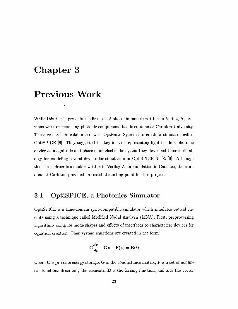
Chapter 3
Previous Work
While this thesis presents the first set of photonic models written in Verilog-A, pre-
vious work on modeling photonic components has been done at Carleton University.
These researchers colaborated with Optiwave Systems to create a simulator called
OptiSPICE [61. They suggested the key idea of representing light inside a photonic
device as magnitude and phase of an electric field, and they described their method-
olgy for modeling several devices for simulation in OptiSPICE [7] [8] [9]. Although
this thesis describes models written in Verilog-A for simulation in Cadence, the work
done at Carleton provided an essential starting point for this project.
3.1 OptiSPICE, a Photonics Simulator
OptiSPICE is a time-domain spice-compatible simulator which simulates optical cir-
cuits using a technique called Modified Nodal Analysis (MNA). First, preprocessing
algorithms compute mode shapes and effects of interfaces to characterize devices for
equation creation. Then system equations are created in the form
dxC- + Gx + F(x) = B(t)
dt
where C represents energy storage, G is the conductance matrix, F is a set of nonlin-
ear functions describing the elements, B is the forcing function, and x is the vector
23

of state variables [7]. The simulator uses Newton-Raphson iterations to find the
DC starting point and numerical integration to find solutions for each time step. It
keeps track of four variables at each node: magnitude and phase of the forward and
backward propagating wave, as shown in Figure 3-1. Using magnitude and phase
as state variables allows efficient use of nonuniform time stepping which outweighs
computation time spent treating interference devices as nonlinear.
Mag Input Forward Direction Output MagFWD FWD
Phase Phase
Meg Output Reverse Direction input Mag
REV REVPhase -Phase
Optical Node A Optical Device Optical Node B
Figure 3-1: Block diagram of a generic optical device showing the four state variablescomputed at each node.
3.2 Magnitude and Phase
In order to simulate light traveling through a photonic link, the electric field needs
to be calculated for various points of the link in various points in time. When light
propagates through a waveguide, the total electric field at a particular point in the
waveguide is described by the equation:
E(t, zo) = EF(t)ej-OF(t)e -jot + EB(t)e3j e (t)ejwot
where Ei(t) is the time varying envelope and qi(t) is the time varying phase of the
forward- or backward-propagating electromagnetic wave. The term ejwot represents
the THz carrier frequency of light. Keeping track of the THz oscillations of the electric
field would force the simulator to use extremely small time steps, which is impractical.
To avoid small time steps, the dependence on carrier frequency is removed, and the
24

equation becomes:
E(t, zo) = EF(t)ej F() + EB(t)ejOB(t)
However, in order to take advantage of WDM, some notion of carrier frequency offset
needs to be retained. Therefore, if the above equation represents the electric field of
one channel with carrier frequency wo, then a second channel with carrier frequency
w, = wo + Aw can be represented as:
E(t, zo) = EF(t)ejOF()e-jAwt + EB(t)eB(t) eiAwt
Since all channels need to fit within one FSR of a ring resonator, the frequency offset
Aw will not be larger than several tens of GHz. Therefore, since AW < wo, the
problem of extremely small time stepping is avoided.
3.3 Optical Devices
The optical devices modeled at Carleton University were categorized into three types:
1) direct elements, in which the signals remain in the optical domain; 2) sources and
detectors, which convert electrical signals into optical signals or vice versa; and 3)
interference elements, which linearly mix optical signals, but they are treated as
nonlinear because trigonometry is used to compute their real and imaginary parts:
Ereai = Emag cos 4, and Eimag = Emag sin 0.
The main example of a direct element is multi mode waveguide which carries n
channels with m bidirectional modes each. However, only a finite set of modes is
excited with a significant amount of energy. Mode excitation is a function of device
geometry and carrier wavelength [7]. Each additional mode included in the simulation
adds two rows (forward and backward propagating) to the systeme equation matrices.
More direct devices include a unidirectional optoisolator, mirrors. Sources and
detectors include the diode laser, continuous-wave source, and photodiode. Interfer-
ence devices include optical connectors, combiners, cross couplers, ring filters. An
optical connector, or optical scattering element (OSE), is a special non-physical de-
25

vice that was modeled for simulating scattering, transmission, and reflection effects
at interfaces of actual devices [8].
26

Chapter 4
Models
This chapter describes how the Verilog-A model of a full photonic link was developed.
First, a laser source was modeled, followed by the creation of a waveguide element.
A version zero photodetector was made to allow output verification, and it was later
refined to have photodiode characteristics. The modulator was also developed in
steps: first a passive ring resonator device was created from a coupler and waveguide,
and then the diode characteristic, which allows modulation, was added. The following
sections will describe the underlying principles of each component model in detail.
4.1 Continuous-Wave Laser Source
The first model that we develop is the continuous-wave laser source because it allows
us to provide an input signal for testing all subsequent components. A symbol of the
laser source illustrating the electrical inputs and two-wire optical output port of the
model is shown in Figure 4-1.
The model has an input port for laser output power and another port for frequency
offset. We also provide an input port for temperature because the output of the
laser is thermally dependent. Although we currently use an external laser source
in the experimental setup, the model is made to support thermal characteristics of
integrated laser sources as well. The relationship between the input signals and the
27

amp
EOU <0:1>TEhe<t:r
Figure 4-1: Symbol for laser model.
complex output is:
E.t = Pmp e g f "AW±Thetr() dT
However, because Verilog-A does not support complex numbers, this translates into
two signals:
Eo< 0 > = Emag Pamp
Eout <1> = Ephase = gj AW + Theater (T) dT
In this equation, Aw is a constant offset frequency which is a parameter that can
be set for each instance of the laser. The gain factor g is used to turn voltage into
frequency because the frequency offset is input using a voltage source, but needs to
be converted to frequency(1V increments laser frequency by g/27r Hz). Pamp is laser
output power in Watts, and Theater is the temperature offset, which is currently used
for thermal control of laser frequency. The output of the laser, Est, is a two-wire bus
in the optical domain, where one wire has the magnitude and the second wire has the
phase of the output laser light.
4.1.1 PolToCart and CartToPol
At this point if the laser frequency had an offset from the nominal center frequency
then the phase would grow linearly with time. It cannot be allowed to grow to infinity,
so it had to be taken modulo 27r/Aw. This caused the phase to be a sawtooth triangle
28

wave with an abrupt jump at every period of 27r/Aw. To the simulator, this was a
very large slope causing convergence problems and aphysical spikes to occur when
simulating elements that involve derivatives.
To combat this problem, we made two blocks to convert the state variables mag-
nitude and phase into real and imaginary parts that oscillate with a period of 27r/Aw
but do not contain discontinuities. The blocks, called PolToCart and Cart ToPol are
shown in Figure 4-2. These blocks were instatiated inside component models every
time a conversion from cartesian to polar or vice versa was needed.
CartToPol PolToCart
Fm , Emag = E eai + Em Ema Em Ereai = Emag COS E r
Eim ' E0 = tan-1 Eimag E0 E , Eimag = Ema, sin E0 E !MT.Ereai
Figure 4-2: Cartesian-to-polar and Polar-to-cartesian converters.
4.2 Waveguide
The model of the waveguide needs to account for three effects that are experienced
by light propagating through the waveguide: time delay, phase delay, and magnitude
attenuation. The model can be broken down into blocks, one for each effect, as shown
in Figure 4-3.
E nMag Attenuation E
Time delay Of eof Lng
EC Phase delay 1 tlhseof Aq(VT)
Figure 4-3: Waveguide modeled as three blocks.
Overall, the relationship between the incoming and outgoing light for the waveg-
uide is described by
Ln ___jot-Ln9
Eou(t) = En(t - L) _ CC
29

The field loss in the waveguide is determined by the attenuation term, e-,L. It is
a function of the attenuation coefficient a and the waveguide length L, parameters
that can be set for each instance. The time delay is the amount of time it takes for
the light to traverse the length of the waveguide: L 2. The phase delay is left as 0 for
the simple waveguide, but it becomes a function of voltage and temperature in the
phase shifter portion of the modulator, discussed in Section 4.4.1.
4.3 Passive Ring Resonator
The ring resonator, or ring filter, is broken down into two blocks to simplify the device
model, as shown in Figure 4-4. One block is simply an instance of a waveguide. Since
the waveguide is circular in this case, the length parameter would be set based on the
desired radius of the ring: L = 27rr. The following section describes how the second
block, the cross-coupler, was implemented.
- Eingin E ringout
Cross Coupler
EwgOut Waveguide E
Figure 4-4: On the left is a ring resonator and on the right is a representation of itas a cross-coupler with a waveguide feedback path.
30
4.3.1 Cross-Coupler
The cross-coupler is a device which has two optical inputs and two optical outputs.
The outputs are a mixture of the inputs:
Egout -it V1 - t2 EringIn
Eringout [1 - t2 -it EwgIn
In that equation, t is the field coupling coefficient which determines the proportions of
each input mixed into the output. One input/output pair of the cross-coupler is the
incoming and outgoing light of the ring filter. The second input/output pair is the
incoming and outgoing light of the waveguide which comprises the circular portion of
the ring.
4.3.2 Thermal Tuning of Ring Resonators
We model the temperature dependence of the ring resonator because temperature
affects the index of refraction and hence the phase delay in the ring waveguide. We
can take advantage of this effect to thermally tune the ring to a particular resonant
frequency. Ring tuning corrects for the process variations that occur during fabri-
cation: the resonance of a ring can shift away from the intended value by as much
as 90GHz ring-to-ring on the same die and 600GHz die-to-die [1]. In addition, the
die experiences time-dependent thermal fluctuations during operation (for example
heating of the die due to power dissipation), which can shift the resonance of a ring
in a CMOS process by -10GHz/K.
There are several ring tuning methods such as fully thermal, full athermalization
using post-process trimming, windowed tuning to nearest resonance taking advantage
of cyclical FSR, and electrically-assited tuning which uses carrier-depletion to further
shift ring resonance [1]. Each method has different implications on the efficiency of
the system as a whole, and therefore it is important to include thermal depencence
and a temperature input port in the ring model. This is currently a work-in-progress,
but the thermal dependence would be modeled by modifying the waveguide model,
31

replacing the group index ng with a thermally dependent index n(T).
4.4 Ring Modulator
The ring modulator encodes data onto the light stream by shifting the ring resonance
in and out of the optical channel. The modulator has optical ports for the incoming
and outgoing light. The electrical ports are the p and n ports of the diode that allows
electrically shifting the resonance. The frequency response of the modulator is shown
in Figure 4-5.
T: Transmis
Insertion Los
To: Transmissivity-before applying bias
Tn: Transmissivityat resonance
AfFWHMH
I
-60 -40 -20
Frequency
ty after applying bias
Extinction Ratio
Ts: Transmissivity/at new resonance
Af
0 20 40
Detuning (GHz)60 80
Figure 4-5: Shift in frequency response of a ring modulatorvoltage across the built-in diode.
due to application of
The figure indicates two key parameters of a modulator: insertion loss and ex-
tinction ratio. Insertion loss (IL) is the ratio of input to output light intensity when
modulator is outputting an optical 1. Extinction ratio (ER) is the ratio of light in-
tensity between an optical 1 and an optical 0. Thus, an extinction ratio of 3dB is a
twofold change in optical power between a 1 and a 0. When designing a modulator, it
32
0
-5
0
C
-10
-15
-20
-25
-30
-80

is possible to calculate the charge needed to deplete from the pn-junction to achieve
the desired ER and IL, and then to calculate the diode bias voltage needed to deplete
that much charge.
In our model of the modulator, we do not compute a static transfer function.
Instead, we split the device into two components, the same way that we did for the
passive ring filter. One component is a cross-coupler. The other component, a phase
shifter, is described in detail in the following section.
4.4.1 Phase Shifter
A modulator contains a ring resonator, so its model has much in common with the
ring resonator model. However, the modulator is an active device because portions of
the waveguide which makes up the ring are lined with diodes. Reverse biasing these
diodes changes the index of refraction, shifting the phase of the light. To model this
effect, the waveguide portion of the ring resonator is replaced with a configurable
phase shifter element to make a modulator, shown in Figure 4-6. The relationship
E E
Cross-Coupler
-- Phase Shifter - Vbas
Figure 4-6: A ring modulator represented as a cross-coupler with a voltage-dependentphase shifter feedback path.
between the input and output light of the phase shifter is described by a similar
equation to the waveguide, but the phase delay is now dependent on voltage applied
33

across the diode:
Eot(t) = |Ei(t - Lnef(c
neff = no + n1Vbias
In this equation, neff is the new, effective index, which is a function of modulator
bias voltage. The coefficients n0 and ni are fitting numbers for the index response
to applied voltage Vbjas. In a more exact iteration of the model, neff will also be a
function of temperature.
Since the phase shifter contains a diode, the relationship between current and
voltage on the diode port is attributed diode characteristics:
dIcap = -(C(Vbias)Vbias)
Ires = I(e ' - 1)
The first equation accounts for the capacitance C(Vbias) of the p-n junction. This
capacitance is a function of bias voltage, and for the first version of the model, the
function is a polynomial fit to data collected from a Sentaurus simulation of a typical
modulator device used on our test chips. The second equation is the Shockley diode
equation, where the reverse-bias saturation current, I,, is a parameter that can be
set for each instance.
4.5 Photodetector
The photodetector contains a PIN diode that senses incoming light. The light im-
pinging on the intrinsic region of the diode induces a photocurrent which is sensed by
a receiver circuit and converted into digital ones and zeros. The left half of Figure 4-7
is a diagram of the photodetector showing three ports: an optical port for incoming
light and two electrical ports for the p and n sides of the diode. The right half of the
figure is a circuit equivalent model of the photodetector, which can be translated into
34

Verilog-A. The photodetector is described by the following set of equations:
P
light
nl photo rs bWs
Figure 4-7: On the left is a diagram of a PIN diode showing generation of photocur-
rent, and on the right is the photodiode equivalent circuit.
Iphoto = Rspv|Ein|12 + VPDbiasRdark
vPDbiPjIres = I,(e n - 1)
dIcap = - (C VPDbias)
EGeAWi
The first equation accounts for the photocurrent produced by incoming light. The
parameter R 8, is the responsivity of the photodiode in Amps/Watt. Rdark is the
equivalent resistance to account for the dark current which is assumed to be steady
and noiseless for now. Finally, Vbia, is the bias voltage on the photodiode.
The second equation is the Shockley diode equation to account for the resistive
portion of the diode model. The third equation accounts for the junction capacitance
in the device. However, this capacitance is computed differently from the junction
capacitance of the modulator diode. The capacitance is determined by the fourth
equation. This capacitor, for the first-order model, is treated as parallel plate due to
the increased distance between the p and n sides because of the intrinsic region in
between. A more exact model would also include the bias-voltage-dependent depletion
region widths, which could add as much as 20% to the intrinsic width, as well as the
parasitic capacitance to substrate.
35

A figure of merit of the photodetector is sensitivity: how much laser power is
needed to reliably resolve each bit. One way in which the photonic link can be
optimized is to find the minimal laser power needed to trigger enough current for
voltage buildup to reach the receiver circuit's sense-amp latching input swing [1].
This is why it is important to continue to refine models of the photodetector and
other elements.
4.6 Optical Combiner
So far, the models have been descibed as if only one wavelength is traveling through
the device. However, this is not going to be the case in practical applications. In order
to provide a way to simulate multiple wavelength channels simultaneously propagating
through a photonic link, an optical combiner element was created.
The combiner takes inputs of light of varying wavelengths that will be present
in the link, and produces an output which is the superposition of the inputs, as
illustrated for two wavelengths in Figure 4-8. Although this figure includes two inputs,
El (t) = Era
E1 (t) - [Eimraum(]I Eirea(t) + E 2real(t)- Emaq.t)) =
[Eitmg~t) Esu~--+ [E.() + E2 ;m, 9 (t)J
E 2rvwq~t)
E 2 (t) = .E2re .. ][E2imq(t)j
Figure 4-8: Optical combiner for superposing several wavelenths of light onto opticaldevices in simulation.
the combiner is actually a parametrized module where any number of inputs can be
used, allowing any number of wavelengths to be combined. However, due to current
limitations of Verilog-A compilation, the model needs to be recompiled each time the
number of inputs is changed.
36

Chapter 5
Simulation Results
Once each component model was written, that component was added as an additional
stage in the photonic link circuit. Simulations were run in Cadence to ensure that
each model produced the correct results. Because the laser model was written first,
it was tested first and used in testing the subsequent components: combiner, waveg-
uide, modulator, and photodetector. Once proven to be functional, the components
were strung together to form a complete photonic link and the link was simulated
transmitting a data pattern. This chapter will showcase the simulation results for
each component and for the link as a whole.
5.1 Verification of Individual Components
The following sections will describe the testbenches, device parameters, and simula-
tions that were performed to verify functionality of each photonic component.
5.1.1 Laser
A laser producing light at the center frequency fo will have a real part that is constant
and equal to the magnitude, and an imaginary part that is constant and zero. If a
frequency offset Af is added, then the phase difference between light of the new
frequency and light of the center frequency will grow linearly in time at the rate Af.
37
When this signal is represented as real and imaginary parts, they are a cosine and
sine wave with period 1/Af, respectively.
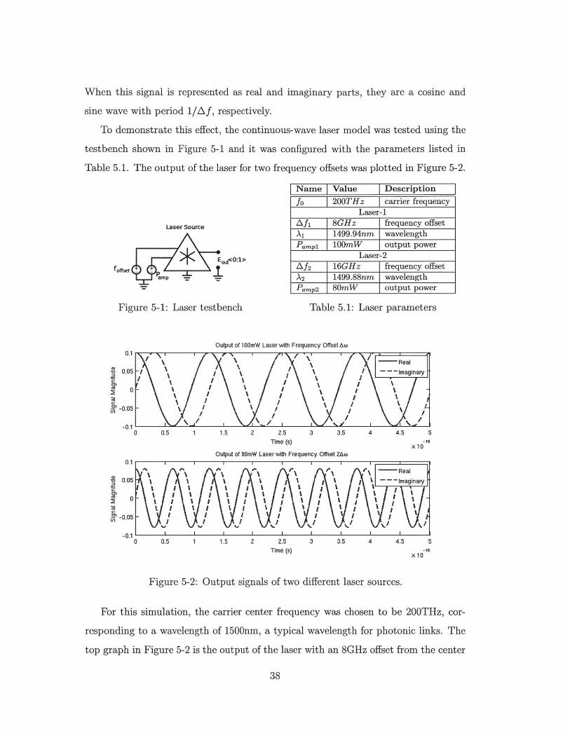
To demonstrate this effect, the continuous-wave laser model was tested using the
testbench shown in Figure 5-1 and it was configured with the parameters listed in
Table 5.1. The output of the laser for two frequency offsets was plotted in Figure 5-2.
Laser Source
amp -
Figure 5-1: Laser testbench
Name Value Description
fo 200THz carrier frequencyLaser-1
Af1 8GHz frequency offsetA, 1499.94nm wavelength
Pampi 100mW output powerLaser-2
Af 2 16GHz frequency offset
A2 1499.88nm wavelengthPamp2 80mW output power
Table 5.1: Laser parameters
Output of 100mW Laser with Frequency Offset Ao0.1
0.05
0
-0.05
-0.1
0.1
0.05
0
-0.05
-0.1
0 0.5 1 1.5 2 2.5 3 3.5 4 4.5 5Time (s) 10
Output of 60mW Laser with Frequency Offset 2Ao
0 0.5 1 1.5 2 2.5Time (s)
3 3.5 4 4.5 5
X1-ie
Figure 5-2: Output signals of two different laser sources.
For this simulation, the carrier center frequency was chosen to be 200THz, cor-
responding to a wavelength of 1500nm, a typical wavelength for photonic links. The
top graph in Figure 5-2 is the output of the laser with an 8GHz offset from the center
38
'V ' Real
-, I ~ ) ~ --- I maginarya)
73~
a
IM
1 1 --- Imaginary
I

frequency, producing 1499.94nm wavelength light. While the difference between the
two wavelengths seems small, it is enough to produce a difference in transmissity of
a ring filter. The bottom graph has twice the frequency offset, 16GHz, and the real
and imaginary parts of the output oscillate twice as fast as in the top graph because
the relative phase of the light grows twice as fast.
Larger frequency offsets will demand smaller time stepping in simulation to cap-
ture the rapid oscillations. This reduces the advantage gained from downconverting
the carrier frequency to baseband, and eliminating the need to simulate 200THz os-
cillations of light. However, there is a limit on how large a frequency offset would
need to be simulated, and it arises from the fact that all frequency channels in a link
have to fit within one FSR. For a ring filter of 5ptm radius, which is typical in modern
processes, the FSR is 2.2THz. If the center frequency is placed in the middle of the
FSR, then the frequency offset can be at most 1.1THz. This still offers a 200-fold
increase in simulation time step over simulating the 200THz carrier frequency.
5.1.2 Combiner
The combiner is a theoretical device that was made to allow simulation of multiple
carrier channels on the same link. This device can superpimpose an arbitrary number
of carrier channels into one set of real and imaginary signals compatible for input into
the modeled photonic devices. Figure 5-3 shows the testbench used for testing the
combiner. Figure 5-4 plots the resulting signal when the two laser sources from Figure
5-2 are superimposed. The combined power and frequency content of the two lasers
is present at the output of the combiner.
5.1.3 Waveguide
A waveguide element transmits an optical signal applying three effects: time delay,
phase delay, and attenuation. The longer the waveguide is, the more pronounced
these effects will be. The waveguide model was tested by comparing a laser input to
the output of two waveguides of different lengths. The testbench is shown in Figure
39

Laser-1
Laser-2 Eu c0:>
A
Figure 5-3: Combiner testbench
Optical Combiner Output
- real
\ imaginary
-L
, 1 1 | 1
I I '-
05 1 1.5 2 2.5Time (s)
3 3.5 4 4.5 5
x 10
Figure 5-4: Combined output of the two lasers from Figure 5-2.
5-5. The laser input is the same as Laser-1 from Table 5.1 and the waveguide is
configured as listed in Table 5.2.
Laser Source
Wavegulde
* E~O:1
f offsett i EI,01
amp
Figure 5-5: Waveguide testbench
Name Value Description
a 288m-1 attenuation coefficientn_ 4.1963 group indexL, 500pm waveguide-1 lengthL2 1mm waveguide-2 length
Table 5.2: Waveguide parameters
This simuation was repeated on a 500pm-long and a 1mm-long waveguide, which
could occur, for example, in an intra-chip link which connects circuits on one side of
the die to circuits on the other side of the die. Figure 5-6 plots the output of each
waveguide. The figure shows that, as expected, the effects become more pronounced
with increasing length: the longer waveguide outputs a smaller amplitude and more
40
0.2
0.1
0
-0.1 I
CD
coCd
U3

delayed version of the input. The real and imaginary parts of the signal experience
the same effect, so to avoid crowding the graph only the imaginary part is shown.
0.1
0.05
0
-0.05-
-0.1
Comparison of Waveguide Outputs
Input
/ / L-500pm
- I. - -/" LL1 !
I \ i
0 0.5 1 1.5 2 2.5Time (s)
3 3.5 4 4.5 5
x 10
Figure 5-6: Output of two different length waveguides.
5.1.4 Modulator
The model of the modulator is able to account for two effects. The first effect is a
shift in resonant frequency when voltage is applied, which allows encoding data onto
the light stream. The second effect is the cyclical FSR, when the ring strikes another
resonance because frequency is offset enough that the integer number of wavelengths
which fit into the ring is higher by one. The testbench used to demonstrate these
effects is shown in Figure 5-7, and the modulator parameter values are listed in Table
5.3.
Liser SourceModulator
qE0
(0:1>
'"t4W
Figure 5-7: Modulator testbench
Name I Value Description
t 0.05 coupling coefficientLtot 30pim ring circumferenceL; 30pm length of doped regionno 2.15 fitting numberni 4x10⁴ fitting number
Oef f 60m-1 field loss coefficientVias OV, 1V diode bias voltage
Table 5.3: Modulator parameters
41

Resonant Frequency Shift
For this simulation, the frequency offset of a 10mW laser source was swept from -
15GHz to +15GHz while the modulator bias voltage was held constant at OV. This
was repeated for a modulator reverse-bias voltage of 1V. The output optical power is
plotted in Figure 5-8.
Ring Modulator Frequency Response
10 . - -- 1 V
- 10
-10 -5 0 5 10Frequency Offset (GHz)
Figure 5-8: Modulator resonance shift due to applied bias.
The resonance of the ring modulator shifts by about 2GHz between the OV and
the 1V modulator bias. This provides an extinction ratio of about 12dB which is
good because the models do not yet account for noise and process variations, which
will degrade the performance. Models also currently do not account for nonlinear
effects of power build-up within the silicon ring.
Free Spectral Range
Ring filters and ring modulators also possess a cyclical FSR which can be useful in
tuning the rings, so it is important for the model to reflect this feature. This model
supports the FSR by dynamically computing the effect of the device on light traveling
through it instead of relying on a pre-defined transfer function. To simulate this effect,
the testbench in Figure 5-7 was used again. Figure 5-9 displays the result of sweeping
the frequency offset of the laser over the range 0-320GHz, without changing the bias
voltage, causing the ring modulator to strike three resonances.
This sweep was performed on a ring of circumference 500pm, which is much larger
than typical, but is convenient for debugging the model. The FSR of a ring is inversely
42

Free Spectral Range (FSR)
10
0 0.5 1 1.5 2 2.5 3Frequency Offset (Hz) x 10
Figure 5-9: Repeating free spectral range of ring resonator.
proportional to its size, so a smaller ring has a larger FSR:
FSR= c
Ltotng
To show a single FSR of the 30um ring more typically used in circuits, the offset
frequency would need to be swept up to 2.4THz. The 500pm ring has an FSR of
140GHz, and it took 4 minutes to run the 0-320GHz sweep for the simulation. For
the 30pm ring, not only would the sweep interval be eight times wider, but smaller
time steps would be required to accomodate the large frequency offset, as discussed
earlier. Given that, the time to run a simulation for the 30pm ring is estimated to
be on the order of 4 hours.
5.1.5 Photodetector
The photodetector is supposed to generate a photocurrent proportional to the inten-
sity of light entering its optical input port. In the testbench shown in Figure 5-10,
the laser ouput power is switched between 1mW and 10mW to stimulate the pho-
todetector with varying intensity of light. The photodetector is configured with the
parameters listed in Table 5.4.
The photodetector consists of a photodiode, so the step response of the device
should have a time constant set by the junction capacitance and series resistance. To
confirm this, Figure 5-11 plots the output of the photodetector when given a square
43

Laserou SorcLser Source
forfset +VP~ba
amp -:-Photodetector
Figure 5-10: Photodetector testbench
Name [Value I DescriptionR ,Pty 1A/W photodiode responsiv-
ityRdark 1MQ dark current equiva-
lent resistance
W_ 700nm intrinsic region width
Ldiode 10pm junction length
Wdode 1pHm junction widthRseries 1kQ series parasitic resis-
tance
Table 5.4: Photodetector parameters
wave input representing 20Gb/s data rate. The time constant, which can be estimated
using the parameters given in Table 5.4 to be 2ps, suggests that the bandwidth of
this photodetector is on the order of hundreds of gigahertz.
Input Laser Power
0.01
0.005 -C.
0 20 40 60 80 100 120Time (ps)
Photodetector Output Current
100
50
0 20 40 60 80 100Time (ps)
140 160 180 200
I120 140 160 100 200
Figure 5-11: Photodetector current for varying input laser power.
5.2 Full Link Simulation
After each of the link components had a working model, the link was simulated as
a whole. Figure 5-12 shows a circuit schematic of the photonic link testbench. No
waveguide element is included because it would only delay and attenuate the signal,
but it will not impact the shape of the signal because the model of the waveguide
does not yet include any frequency-selective filtering effects. Table 5.5 summarises
the device parameters used for this simulation. First, a basic test of the link's ability
44

to transmit data was performed. Next, a more complex data stream was transmitted
to produce an eye diagram.
Laser Source
amp
Modulator
Vb~as
,out
Photodetector
Figure 5-12: Complete photonic link testbench
5.2.1 Transient Analysis
First, a basic transient simulation was performed to see how the link would respond to
on-off keying of light by the modulator. The modulator was driven by a 10GHz square
wave alternating between OV and 1V, while the laser frequency was held constant.
Three signals are plotted in Figure 5-13: the voltage across the modulator diode, the
optical power coming out of the modulator through port, and the current out of the
photodetector.
In Figure 5-13, the output current of the photodetector closely matches the mod-
ulator output optical power which is the input to the photodetector. As discussed in
Section 5.1.5, the photodetector has a fast response. Hence, the bandlimited shape of
the output signal arrises from the modulator. For the modulator in this simulation,
the electrical response of the diode looks much less bandlimited than the optical re-
sponse, suggesting that the optical response of this modulator is the limiting factor
on link data rate.
45

Name Value Description
LaserPamp 10mW optical power
fo 200THz center carrier frequencyAf 0 frequency offsetModulator
t 0.05 field coupling coefficientLtot 30pm circumference of ring
Li 30pm doped region length
c'eff 60m- 1 field loss coefficientno 2.15 index fitting numberni 4x10- 5 index fitting number
R kQ parasitic series resistancePhotodetector
Rs5PtY 1A/W responsivityRdark lMQ dark current equivalent resistance
Wi 700nm intrinsic widthLdiode 10Im junction length
Wdiode 1pm junction widthRseries lkQ parasitic series resistance
I5 10~14 A reverse bias saturation current
Table 5.5: Summary of device parameters
46

Modulator Drive Voltage
-1L
0 0.5 1 1.5 2 2.5 3 3.5 4 4.5 5Time (ns)
Modulator Output Power5100
0 00 0.5 1 1.5 2 2.5 3 3.5 4 4.5 5
TIme (ns)
Photodetector Output Current100 I I I I ' I I I
00 0.5 1 1.5 2 2.5 3 3.5 4 4.5 5Time (ns)
Figure 5-13: Transient simulation of the photonic link.
5.2.2 Eye Diagram
After confirming basic operation, the modulator was driven with a more complex data
pattern. The data pattern, 0001011100, was designed to include every two-bit state
transition to illustrate the effect of inter-symbol interference (ISI) on the link. The
laser frequency was held constant while the modulator bias voltage changed between
0V and 1V with a 10GHz data rate. Figure 5-14 shows the same signals of interest as
Figure 5-13. Figure 5-15 shows an eye diagram of the photodetector output current.
47

Modulator Drive Voltage
-
r
-0
0 1 2 3 4 5Time (ns)
Modulator Output Power
6 7 0 9 10
100
50
0 00 1 2 3 4 5 6 7 a 9 10
Time (ns)Photodetector Output Current
O0r A 'i I j I * I I
0 1 2 3 4 5Time (ns)
J~yj6 7 a 9 10
Figure 5-14: Transient simulation of the photonic link.
0.
0.
0.
0.
0.
0.
0.
0.
0.
Eve DIamm
7
6 -
5-
4A-
3 -
2 -
0z 3 7
1 -
Time (s)
Figure 5-15: Eye diagram of photodetector output.
48
"'Vt,.SI I
I
E 50 -
U
1
.,d,
.1d'o

Chapter 6
Conclusion
Photonic links are a developing technology that promises to resolve the interconnect
bottleneck of modern integrated circuits by leveraging wavelength-division multiplex-
ing to achieve high bandwidth density and low energy per bit. Before photonic links
can become a mainstream technology, models must be developed to facilitate the de-
sign of circuits and systems that use photonic devices. This thesis presented a library
of first-pass Verilog-A models for components of a photonic link. The functional-
ity of the models was demonstrated through a series of device and link simulations.
These models are compatible with circuit simulators, eliminating the need for using
a separate optical simulator, and allowing simulation of photonic and electronic sys-
tems side-by-side to achieve higher accuracy. These models will aid in the design and
optimization of photonic link technology.
6.1 Future Work
Although a model has been created for each component of the photonic link, much
work remains to be done. The second-pass models will consider more effects, such
as interference and scattering at interfaces of devices, and noise and electromagnetic
interference. In addition, support for thermal tuning needs to be added to allow fur-
ther exploration of the tuning strategies presented in [1]. Moreover, since multiple
modes of a propagating wave can be excited for a given wavelength and device ge-
49

ometry, support for computing the effect of higher order modes should be added like
discussed in [7]. Finally, these models can be expanded to augment the CAD design
flow if device layouts are added to each component in the library.
50

Appendix A
Verilog-A Code
A.1 Optical Discipline
// Opticalnature Efield
units = "E";access = E;
'ifdef EPHASEABSTOL
abstol = 'EPHASEABSTOL;'else
abstol = le-6;'endif
endnature
// Conservative discipline
discipline optical
potential Efield;
enddiscipline
A.2 Laser
module laser-cw(gnd, out, Htemp, ampin);
inout gnd;
input Htemp, ampin; // temp relative to roomtemp
electrical ampin;
output [0:1] out;
51

thermal
opticaloptical
Htemp;gnd;
[0:1] out;
//Internal nodes
optical [0:1] outP2C;
parametersreal gain=1e10;
real offsetfreq=0;
// gain of temperature to frequency
// offset from center frequency
analog begin
// magnitude
E(outP2C[1],gnd) <+ V(ampin);// phase
E(outP2C[0],gnd) <+ gain*idt (Temp(Htemp)+offsetfreq*2*'MPI,0)end
pol2cart outconv(outP2C, out, gnd);
endmodule
A.3 Combiner
module combiner(in, out,inout optical.gnd;
input [0:3] in;
output [0:1] out;
optical optical-gnd;
optical [0:3] in;
optical [0:1] out;
// Internal nodes
real outr, outi; //genvar i; //
optical-gnd);
Output real and imaginary partsIndex in for-loop
analog begin
outr = 0; // Reset running totals
outi 0;for (i=0; i<3; i=i+2) begin
// Add ith input pair to running sumsoutr = outr + E(in[i+1],optical-gnd);outi = outi + E(in[i],optical.gnd);
end
52
// Deviceparameterparameter

E(out[1],optical-gnd) <+ outr;
E(out[0],optical-gnd) <+ outi;
end
endmodule
A.4 Waveguide
module waveguide(optgnd, inlig, outlig );inout optgnd;
input [0:1] inlig;output [0:1] outlig;
optical optgnd;
optical [0:1] outlig, inlig;
// Device parameters
parameter real L = 0.0005; // waveguide legnth [m]
parameter real ng = 4.1963; // group index
parameter real alphaA = 287.6; // Field loss coefficient [m^-1]
// Internal nodes
optical [0:1] outNodly; // cart
optical [0:1] ringres;
optical [0:1] ringConv;
pol2cart convsl(ringres, ringConv, optgnd);
cartmul muloutl(ringConv, inlig, outNodly);
analog begin
//calculate the derivative term:
E(ringres[0], optgnd) <+ 0.0;
E (ringres [1] , optgnd) <+ exp (-alphaA*L);
E(outlig[0], optgnd) <+ absdelay(E(outNodly[0] ,optgnd) ,L*ng/'PC);
E(outlig[1], optgnd) <+ absdelay(E(outNodly[1],optgnd),L*ng/'PC);
end
endmodule
A.5 Coupler
module coupler(optgnd, inligi, inlig2, outligi, outlig2);
input [0:1] inligi, inlig2;
53

inout optgnd;
output [0:1] outligi, outlig2;
optical optgnd;
optical [0:1] inligi, outligi, inlig2, outlig2;
// Device parameters
parameter real t = 0.5; // Field coupling coefficient
// Internal nodes
optical [0:1] Xcoup;
optical [0:1] Xthru;
optical [0:1] inligiX;
optical [0:1] inlig2X;
optical [0:1] inligiT;
optical [0:1] inlig2T;
optical [0:1] Xcoup2;
analog begin
E(Xcoup[0], optgnd) <+ 0.0;
E(Xcoup[1], optgnd) <+ -t;E(Xcoup2[0], optgnd) <+ 0.0;
E(Xcoup2[1], optgnd) <+ -t;
E(Xthru[0], optgnd) <+ sqrt(1-t*t);E(Xthru[1], optgnd) <+ 0;
end
cartmul inlX(inligl, Xcoup2, inligiX);
cartmul in2X(inlig2, Xcoup, inlig2X);
cartmul inlT(inligl, Xthru, inlig1T);
cartmul in2T(inlig2, Xthru, inlig2T);
cartadd combl(inliglT, inlig2X, outligi);
cartadd comb2(inliglX, inlig2T, outlig2);
endmodule
A.6 Phase Shifter
module phaseshifter(vtop, vbot, optgnd, inlig, outlig);
input vtop, vbot;
input [0:1] inlig;
inout optgnd;
output [0:1] outlig;
electrical vtop, vbot;
optical optgnd;
54

optical [0:1] outlig,branch (vtop,vbot) res,
// Deviceparameter
parameterparameterparameterparameterparameterparameter
parametersreal Lreal ngreal alphaeff
real nO
real n1
real length
real Is
500e-6;
4.2543;0;0.0;0.01;10e-6;le-14;
// Derived Parameter Declarationsreal Va;
real neff;
real c, v, capacitance;
real a6, a5, a4, a3, a2, al, aO;
////-//-//I//I//,//
Ring length [m]
Group index
Field loss coeffcient [m^-1]
Index fitting number
Index fitting number
Length of diode [m]
Rev-bias saturation current [A]
// Coefficients for polynomial
// Internal nodes
optical [0:1] TshifterP;
optical [0:1] TshifterC;
optical [0:1] outNodly;
pol2cart convsl(TshifterP, TshifterC, optgnd);
cartmul multoutl(TshifterC, inlig, outNodly);
analog begin
// initialize constants
a6 = 0.0005e-15;a5 = 0.0070e-15;a4 = 0.0384e-15;a3 = 0.0921e-15;a2 = 0.0983e-15;at = 0.1131e-15;aO = 0.3628e-15;
// Calculate junction capacitance
// if V(p,n) is outside the range of data then capacitance clips
v=V(cap);
if (v>0)
c = aO;else if (v<-4)
c = a6*pow(-4,6)+a5*pow(-4,5)+a4*pow(-4,4)+a3*pow(-4,3)+a2*pow(-4,2)+al*-4+aO;
else
55
inlig;cap;

c = a6*pow(v,6)+a5*pow(v,5)+a4*pow(v,4)+a3*pow(v,3)+a2*pow(v,2)+al*v+aO;
// c is capacitance per [um] of length
// convert length from [m] to [um] and find total capacitance
capacitance = length*1e6*c;
// Diode equations
I(cap) <+ ddt(capacitance*V(cap));
I(res) <+ Is*(limexp(V(res)/($vt))-1);
// Calculate optical outputs
neff = nO+nl*V(vtop,vbot);
E(TshifterP[0], optgnd) <+ ((neff*L*2*'MPI)*
('GFREQ)/'PC)%(2*'MPI);E(TshifterP[1], optgnd) <+ exp(-alphaeff*L);
E(outlig[0], optgnd)<+absdelay(E(outNodly[0],optgnd),L*ng/'PC);
E(outlig[1], optgnd)<+absdelay(E(outNodly[1],optgnd),L*ng/'PC);
end
endmodule
A.7 Photodetector
module photodetector(optgnd, vtop, vbot, inlig);
input [0:1] inlig;
inout optgnd;
inout vtop, vbot;
electrical vtop, vbot;
optical [0:1] inlig;
optical optgnd;
branch (vtop, vbot) res, cap, photo;
// Device parametersparameter real Rspvty = 1.0;
parameter real Rdark = 1e6;parameter real Wi = 700e-9;parameter real len = 10e-6;
parameter real wid = le-6;
parameter real Is = le-14;parameter real Rs = 1e3;
// Photodiode responsivity
// Dark current equiv resistance [Ohm]
// Width of intrinsic region [m]
// Length of photodiode [m]
// Width of photodiode Em]
// Rev-bias saturation current [A]
// Series resistance [Ohm]
// Derived Parameter Declarations
real Optmag;
56

// Dielectric constant of germanium
// Junction capacitance
analog begin
eGe = 16*'PEPSO;Cj = eGe*len*wid/Wi; // model as parallel plate for now
// Diode equations
I(cap) <+ ddt(Cj * V(cap));I(res) <+ Is*(limexp(V(res)/($vt))-1);
// Calculate photocurrent
Optmag = E(inlig[1], optgnd)*E(inlig[1], optgnd)+E(inlig[O], optgnd)*E(inlig[O], optgnd);
I(photo) <+ Rspvty*Optmag+V(photo)/Rdark;
end
endmodule
57
real eGe;real Cj;

58

Bibliography
[1] C. Sun, Design space exploration of photonic interconnects. M.S. thesis. Cam-bridge, Massachusetts: MIT, 2011. [Online]. Available: DSpacecQMIT.
[2] J. Leu, A 9GHz injection locked loop optical clock receiver in 32-nm CMOS.M.S. thesis. Cambridge, Massachusetts: MIT, 2010. [Online]. Available:
DSpace©MIT.
[3] B. Moss, High-speed modulation of resonant CMOS photonic modulators in deep-
submicron bulk-CMOS. M.S. thesis. Cambridge, Massachusetts: MIT, 2009. [On-line]. Available: DSpaceOMIT.
[4] M. Georgas, An optical data receiver for integrated photonic interconnects.
M.S. thesis. Cambridge, Massachusetts: MIT, 2009. [Online]. Available:DSpace©MIT.
[5] K. Kundert and 0. Zinke, The Designer's Guide to Verilog AMS. Boston: Kluwer
Academic Publishers, 2004.
[6] T. Smy, M. Freitas, and V. Ambalavanar, "Self-Consistent Opto-Thermal-Electronic Simulation of Micro-Rings for Photonic Macrochip Integration,"
[7] P. Gunupudi, T. Smy, J. Klein, and J. Jakubczyk, "Self-consistent simulation
of opto-electronic circuits using a modified nodal analysis formulation," IEEE
Transactions on Advanced Packaging PP(99), 1-15 (2010).
[8] T. Smy, P. Gunupudi, S. McGary, and N. Ye, "Circuit-level transient simulation
of configurable ring resonators using physical models," J. Opt. Soc. Am. B 28,1534-1543 (Jun 2011).
[9] T. Smy and P. Gunupudi, "Robust Simulation of Opto-electronic Systems byAlternating Complex Envelope Representations," IEEE Transactions on TCAD- Accepted for publication.
[10] J. Orcutt, et. al., "An Open Foundry Platform for Hight-Performance Electronic-
Photonic Integration," Optical Society of America, 2012.
[11] M. Georgas, J. Orcutt, R. J. Ram, and V. Stojanovic, "A Monolithically-Integrated Optical Receiver in Standard 45-nm SOI," European Solid-State Cir-
cuits Conference, Helsinki, Finland, 4 pages, September 2011.
59

[12] M. Georgas, J.C. Leu, B. Moss, C. Sun, and V. Stojanovic, "Addressing Link-Level Design Tradeoffs for Integrated Photonic Interconnects," IEEE CustomIntegrated Circuits Conference, 8 pages, San Jose, CA, September 2011.
[13] S. M. Sze, K. K. Ng, "Photodiodes" in Physics of Semiconductor Devices, 3rded. Hoboken, N.J. : Wiley-Interscience, 2007, ch. 13, sec. 3.
60