Embed Size (px)
Citation preview

Modeling of Voltage Source Converter
Based HVDC Transmission
System in EMTP-RV
by
Hiteshkumar Patel
A Thesis Submitted in Partial Fulfillment
of the Requirements for the Degree of
Master of Applied Science
in
The Faculty of Engineering and Applied Science
Electrical and Computer Engineering
University of Ontario Institute of Technology
August, 2010
© Hiteshkumar Patel, 2010

ii
CERTIFICATE OF APPROVAL
Submitted by [Hiteshkumar, Patel]
In partial fulfillment of the requirements for the degree of
[Master of Applied Science] in [Electrical and Computer Engineering]
Date of Defense: [2010/08/17]
Thesis title: Modeling of Voltage Source Converter Based HVDC Transmission System in EMTP-RV
The undersigned certify that the student has presented [his] thesis, that the thesis is acceptable in form and content and that a satisfactory knowledge of the field covered by the thesis was demonstrated by the candidate through an oral examination. They recommend this thesis to the Office of Graduate Studies for acceptance.
Examining Committee
_________________________________________ [first name, last name] Chair of Examining Committee _________________________________________ [first name, last name] External Examiner
_________________________________________ [Vijay, Sood]
Research Supervisor
_________________________________________ [first name, last name]
Examining Committee Member
_________________________________________ [first name, last name]
Examining Committee Member
As research supervisor for the above student, I certify that I have read and approved changes required by the final examiners and recommend the thesis for acceptance:
_________________________________________ [Vijay, Sood] Research Supervisor

iii
AUTHOR'S DECLARATION
I hereby declare that I am the sole author of this thesis. This is a true copy of the thesis,
including any required final revisions, as accepted by my examiners.
I understand that my thesis may be made electronically available to the public.
Hiteshkumar Patel

iv
Abstract
Voltage Source Converter (VSC) applications include but are not limited to HVDC,
Flexible AC Transmission System (FACTS) devices such as STATCOM, SSSC, UPFC and
Wind generators and active filters. The VSC based HVDC system is a feasible option for
bulk power transmission over long or short distances and the grid integration of renewable
energy sources in existing transmission and distribution systems.
The main requirement in a power transmission system is the precise control of active and
reactive power flow to maintain the system voltage stability. The VSC operating with the
specified vector control strategy can perform independent control of active/reactive power at
both ends. This ability of VSC makes it suitable for connection to weak AC networks or even
dead networks i.e. without local voltage sources. For power reversal, the DC voltage polarity
remains the same for VSC based transmission system and the power transfer depends only on
the direction of the DC current. This is advantageous when compared to the conventional
Current Source Converter (CSC) based HVDC system. Furthermore, in case of VSC, the
reactive power flow can be bi-directional depending on the AC network operating conditions.
In this thesis, a 3-phase, 2-level, 6-switch VSC connected to an active but weak AC
system at both ends of the HVDC link is developed using EMTP-RV. The VSC-HVDC
transmission system model is developed using both direct control and vector control
techniques. The direct control method is an approximate method in which the active power,
AC voltages at both ends of HVDC link and DC link voltage are controlled directly by using
PI-controllers. In vector control method, closed loop feed-forward control system is used to
control the active power, reactive power at both ends and DC voltage.

v
By comparing the simulation results, it is concluded that the vector control method is
superior to the direct control because of the removal of the coupling between control
variables to achieve the independent control of active and reactive powers at both ends of the
HVDC link.

vi
Acknowledgements
I would like to express my deep appreciation for my supervisor, Dr. Vijay Sood, who is
leading the electrical power engineering program at UOIT. Without his supervision and
consistent guidance, completing this thesis would not have been possible.
I am also thankful to my colleagues who have inspired me and make me laugh at critical
phases during the entire study period. Thanks to the library staff for providing support
throughout the whole program.
A special thanks to my wife and daughter for their support and encouragement. Without
their unconditional, pure love, I would not achieve such a challenging target. Their powerful
dreams are my fuel to make everything happen.
At last, I cannot forget to mention the inspiration I got from God and my final
appreciation is to those who I may have failed to mention.

vii
Dedication
This thesis is dedicated to my parents (Baldev Patel and Savita Patel), without their
continuous love and inspiration it would not have been possible to complete this work.
viii
Table of Contents
Author’s Declaration ................................................................................................................ iii
Abstract .................................................................................................................................... iv
Acknowledgements .................................................................................................................. vi
Dedication. .............................................................................................................................. vii
Table of Contents ................................................................................................................... viii
List of Figures ........................................................................................................................ xiii
List of Tables ........................................................................................................................ xvii
Chapter 1 Introduction .............................................................................................................. 1
1.1 Background ..................................................................................................................... 1
1.2 Related literature review ................................................................................................. 3
1.3 Scope of the project ......................................................................................................... 9
1.4 Objective of the thesis ................................................................................................... 10
1.5 Outline of the chapters .................................................................................................. 11
1.6 Summary ....................................................................................................................... 12
Chapter 2 VSC-HVDC System ............................................................................................... 13
2.1 Introduction ................................................................................................................... 13
2.2 VSC-HVDC system ...................................................................................................... 14
2.2.1 AC shunt RLC-filters.............................................................................................. 15
2.2.2 Converter Transformer ........................................................................................... 15
ix
2.2.3 Voltage Source Converter ...................................................................................... 15
2.2.4 DC transmission ..................................................................................................... 16
2.2.5 DC capacitors ......................................................................................................... 17
2.3 Topologies of the VSC .................................................................................................. 18
2.3.1 Two-level voltage source converter ....................................................................... 18
2.3.2 Multi-level voltage source converter ...................................................................... 19
2.3.3 Multi-pulse topologies ............................................................................................ 23
2.4 PWM for VSC ............................................................................................................... 24
2.4.1 Sinusoidal PWM ..................................................................................................... 24
2.5 VSC-HVDC Operation ................................................................................................. 26
2.5.1 Operating principle of VSC-HVDC ....................................................................... 26
2.5.2 Four quadrant operation of VSC ............................................................................ 28
2.5.3 Rectifier- Inverter operation of VSC ...................................................................... 30
2.6 Summary ....................................................................................................................... 32
Chapter 3 Control of VSC-HVDC System ............................................................................. 33
3.1 Introduction ................................................................................................................... 33
3.2 Direct control method.................................................................................................... 34
3.3 Vector control method ................................................................................................... 35
3.4 Limitations .................................................................................................................... 39
3.5 Outer controller ............................................................................................................. 40
3.5.1 DC voltage controller ............................................................................................. 40
x
3.5.2 Active power controller .......................................................................................... 42
3.5.3 Reactive power controller ....................................................................................... 42
3.6 Summary ....................................................................................................................... 45
Chapter 4 Methodology .......................................................................................................... 46
4.1 Introduction ................................................................................................................... 46
4.2 Power system modeling ................................................................................................ 46
4.2.1 Modeling of weak AC networks ............................................................................. 47
4.2.2 Modeling of converter transformer ......................................................................... 47
4.2.3 Modeling of AC shunt RLC-Filters ........................................................................ 48
4.3 Converter Modeling (Rectifier and Inverter) ................................................................ 51
4.3.1 Converter topology modeling ................................................................................. 51
4.3.2 IGBT-Diode module modeling ............................................................................... 52
4.4 DC capacitors and transmission system modeling ........................................................ 54
4.5 Control system modeling .............................................................................................. 56
4.5.1 Carrier frequency generation .................................................................................. 56
4.5.2 Sinusoidal pulse width modulation (SPWM) ......................................................... 57
4.5.3 Direct Control system modeling ............................................................................. 58
4.5.4 Vector control system modeling ............................................................................. 63
4.5.5 PI-Controller Gains................................................................................................. 70
4.6 Summary ....................................................................................................................... 74
Chapter 5 Simulation Results and Analysis ............................................................................ 75
xi
5.1 Introduction ................................................................................................................... 75
5.2 Steady state operation-Direct control method ............................................................... 76
5.2.1 Case study-1 ........................................................................................................... 76
5.2.2 Case-study-2 ........................................................................................................... 77
5.3 Step changes-Direct control method ............................................................................. 78
5.4 Active power flow reversal-Direct control method....................................................... 80
5.5 Steady state operation -vector control method .............................................................. 82
5.5.1 Case study-1 ........................................................................................................... 82
5.5.2 Case study-2 ........................................................................................................... 83
5.5.3 Case study-3 ........................................................................................................... 84
5.5.4 Case study-4 ........................................................................................................... 85
5.6 Step changes -vector control method ............................................................................ 86
5.7 Active and reactive power reversal -vector control method ......................................... 89
5.8 Comparison between direct and vector control technique ............................................ 91
5.9 Effect of DC capacitance on VSC-HVDC performance ............................................... 92
5.10 Summary ..................................................................................................................... 95
Chapter 6 Fault Analysis ......................................................................................................... 96
6.1 Introduction ................................................................................................................... 96
6.2 Fault analysis at VSC1 ................................................................................................... 96
6.2.1 Single line to ground (SLG) fault at VSC1 ............................................................. 97
6.2.2 Asymmetrical double line to ground (DLG) fault on AC filter bus at VSC1 ......... 98

xii
6.2.3 Symmetrical three lines to ground (TLG) fault on AC filter bus at VSC1 ............. 99
6.3 Fault analysis at VSC2 ................................................................................................. 101
6.3.1 Single line to ground fault at VSC2 ...................................................................... 101
6.3.2 Asymmetrical double line to ground fault on AC filter bus at VSC2 ................... 102
6.3.3 Symmetrical three lines to ground fault on AC filter bus at VSC2....................... 103
6.4 Fault at DC transmission system ................................................................................. 105
6.5 Summary ..................................................................................................................... 105
Chapter 7 Conclusions and Future work ............................................................................... 106
7.1 Conclusions ................................................................................................................. 106
7.2 Future work ................................................................................................................. 109
Appendix A: Per Unit System Representation................................................................... 115
Appendix B: Filter Design Calculations…...…...………………………………………117
Appendix C: ABC to dq Conversions….……………………………………………….119
Appendix D: EMTP-An Overview…….………………………………………………123
Appendix E: List of Publications………………………………………………………124
xiii
List of Figures
Figure 2.1: Single Line Diagram of VSC-HVDC System .................................................... 14
Figure 2.2: 2-Level, 6-Switch, 3-phase Converter Topology ............................................... 18
Figure 2.3: 3-Level, NPC-Converter Topology .................................................................... 20
Figure 2.4: 3-Level, Flying Capacitor Converter Topology ................................................. 21
Figure 2.5: 3-Level, Actively Neutral Point Clamped Converter Topology ........................ 22
Figure 2.6: 5-Level, Cascaded H-bridge Converter Topology ............................................. 22
Figure 2.7: Comparison between Sinusoidal and Triangular waveform and PWM Signals 25
Figure 2.8: Single Line Diagram for VSC-HVDC Operating Principle ............................... 26
Figure 2.9: P-Q Circle Diagram for VSC Operation ............................................................ 29
Figure 2.10: VSC Operation as Rectifier or Inverter ............................................................ 30
Figure 2.11: VSC Operation as a Rectifier ........................................................................... 31
Figure 2.12: VSC Operation as an Inverter .......................................................................... 32
Figure 3.1: VSC-HVDC Control System.............................................................................. 34
Figure 3.2: Vector Control System of VSC-HVDC System ................................................. 36
Figure 3.3: Active and Reactive Power Control System ...................................................... 44
Figure 4.1: Converter Transformer Model............................................................................ 48
Figure 4.2: EMTP-RV Filter Modeling and Frequency Scan graph ..................................... 49
Figure 4.3: Converter Model in EMTP-RV .......................................................................... 52
Figure 4.4: IGBT Valve Modeling........................................................................................ 53

xiv
Figure 4.5: DC Transmission System Modeling................................................................... 55
Figure 4.6: Carrier Frequency Generation Block ................................................................. 56
Figure 4.7: SPWM Block ...................................................................................................... 58
Figure 4.8: Angle delta block................................................................................................ 59
Figure 4.9: Active power control block for direct control method ....................................... 59
Figure 4.10: AC voltage control block at VSC1 for direct control ....................................... 60
Figure 4.11: DC voltage control block at VSC2 for direct control ....................................... 61
Figure 4.12: AC voltage control at VSC2 for direct control ................................................. 61
Figure 4.13: Direct control system for VSC-HVDC ............................................................ 62
Figure 4.14: Modulation Index and Angle Delta Block ....................................................... 64
Figure 4.15: Outer current controller loop for active power control block .......................... 64
Figure 4.16: Inner current controller loop for active power control block ........................... 65
Figure 4.17: Outer current controller loop for reactive power control block ....................... 66
Figure 4.18: Inner current controller loop for reactive power control block ........................ 67
Figure 4.19: Outer current controller for DC voltage control system ................................... 67
Figure 4.20: Inner current controller for DC voltage control system ................................... 68
Figure 4.21: Inner current controller loop for reactive power control block ........................ 69
Figure 4.22: Outer current controller loop for reactive power control block ....................... 69
Figure 4.23: VSC-HVDC model created using EMTP-RV software package ..................... 71
Figure 4.24: Rectifier Control Block of Proposed VSC-HVDC model ................................ 72
Figure 4.25: Inverter control block for proposed VSC-HVDC model ................................. 73

xv
Figure 5.1: Steady-state operation of VSC-HVDC with direct control method (a) 1 pu active
power flow from VSC1 to VSC2 (b) 1 pu AC bus voltage at VSC1 filter bus (c) 1 pu AC bus
voltage at VSC2 filter bus (d) 1 pu DC link voltage ............................................................... 76
Figure 5.2: Steady-state operation of VSC-HVDC with direct control method (a) 1 pu active
power flow from VSC2 to VSC1 (b) 1 pu AC bus voltage at VSC1 filter bus (c) 1 pu AC bus
voltage at VSC2 filter bus (d) 1 pu DC link voltage ............................................................... 77
Figure 5.3: Dynamic-state operation of VSC-HVDC with direct control method (a) 0.5 pu
active power flow from VSC2 to VSC1 (b) 1 pu AC bus voltage at VSC1 filter bus (c) 1 pu
AC bus voltage at VSC2 filter bus (d) 1 pu DC link voltage .................................................. 79
Figure 5.4: Steady-state operation of VSC-HVDC with direct control method (a) Initially
0.5 pu active power flow from VSC2 to VSC1 (b) Initially 1 pu AC bus voltage at VSC1 filter
bus (c) Initially 1 pu AC bus voltage at VSC2 filter bus (d) DC link voltage is maintained
constant at 1 pu ....................................................................................................................... 81
Figure 5.5: Steady-state operation of VSC-HVDC (a) 0.45 pu active power flow from VSC2
to VSC1 (b) Reactive power of 0 pu at VSC1 (c) DC voltage of 1 pu in DC link (d) Reactive
power of 0 pu at VSC2 ............................................................................................................ 83
Figure 5.6: Steady-state operation of VSC-HVDC (a) 0.45 pu active power flow from VSC1
to VSC2 (b) Reactive power of 0 pu at VSC1 (c) DC voltage of 1 pu in DC link (d) Reactive
power of 0 pu at VSC2 ............................................................................................................ 84
Figure 5.7: Full load active power flow (a) 1 pu active power flow from VSC1 to VSC2 (b)
0.65 pu reactive power flow from VSC1 to AC system (c) DC voltage of 1 pu in DC link (d)
0.45 pu reactive power flow from AC system to VSC2 .......................................................... 85
Figure 5.8: Full load active power flow (a) 1 pu active power flow from VSC2 to VSC1 (b)
0.25 pu reactive power flow from VSC1 to AC system (c) DC voltage of 1 pu in DC link (d)
0.5 pu reactive power flow from VSC2 to AC system ............................................................ 86
Figure 5.9: Step changes in the active power, reactive power and DC voltage (a) 0.5 pu
active power flow from VSC2 to VSC1 (b) 0.5 pu reactive power flow from AC system to

xvi
VSC1 (c) DC voltage of 1 pu in DC link (d) 0.5 pu reactive power flow from VSC2 to AC
system ..................................................................................................................................... 88
Figure 5.10: Active and reactive power reversal (a) Initial active power flow of 0.5 pu from
VSC2 to VSC1 (b) Initial reactive power of 0.15 pu flow from AC system to VSC1 (c) Initial
reactive power of -0.5 pu flow from VSC2 to AC system (d) DC voltage of 1 pu in DC link 90
Figure 5.11: Step changes with the DC capacitance of 100µF at each terminal .................. 93
Figure 5.12: Step changes with the DC capacitance of 200µF at each terminal .................. 93
Figure 5.13: Step changes with the DC capacitance of 300µF at each terminal .................. 94
Figure 5.14: Step changes with the DC capacitance of 400µF at each terminal .................. 94
Figure 6.1: SLG fault at VSC1 converter transformer .......................................................... 97
Figure 6.2: DLG fault at VSC1 converter transformer .......................................................... 99
Figure 6.3: TLG fault at VSC1 converter transformer ........................................................ 100
Figure 6.4: SLG fault at VSC2 converter transformer ........................................................ 102
Figure 6.5: DLG fault at VSC2 converter transformer ........................................................ 103
Figure 6.6: TLG fault at VSC2 converter transformer ........................................................ 104
Figure 61: ABC to dq conversion block modeling in EMTP-RV ........................................ 119
Figure 62: Phasor diagram for relationship between ABC and αβ ....................................... 120
Figure 63: Phasor diagram for relationship between ABC, dq and αβ quantities ................ 122
xvii
List of Tables
Table 4-1 Filter Ratings .......................................................................................................... 50
Table 4-2 DC Cable RLC-Parameters .................................................................................... 55
Table 4-3 VSC-HVDC PI-controller gains ............................................................................. 70
Table 5-1: Parameters of VSC-HVDC Simulation Model ................................................... 75
Table B-7-1: Filter ratings at VSC1 ...................................................................................... 117
Table B-7-2: Filter ratings at VSC2 ...................................................................................... 117

xviii
List of Acronyms
AC Alternating Current
ANPC Actively Neutral Point Clamped
B-B Back to Back
CC Current Controller
CSC Current Source Converter
DC Direct Current
DLG Double Line to Ground
EMT Electromagnetic Transient
EMTP-RV Electromagnetic Transient Program Restructured Version
FACTS Flexible AC Transmission System
FC Flying Capacitor
GTO Gate Turn-off Thyristor
HV High Voltage
HVDC High Voltage Direct Current
IGBT Insulated Gate Bi-polar Transistor
LCC Line Commutated Converter
MOSFET Metal Oxide Field Effect Transistor
NPC Neutral Point Clamped
PI Proportional-Integral
PSCAD Power System Computer Aided Design
PWM Pulse Width Modulation
R & D Research and Development
SCR Short Circuit Ratio

xix
SLD Single Line Diagram
SLG Single Line to Ground
SPWM Sinusoidal Pulse Width Modulation
STATCOM Static Synchronous Compensator
SSSC Static Synchronous Series Compensator
SVC Static Var Compensator
TLG Triple Line to Ground
UPFC Unified Power Flow Controller
VSC Voltage Source Converter

1
Chapter 1
Introduction
1.1 Background
The continuous increase in global power demand has fuelled the R & D of new
technologies for bulk power transmission with improved reliability and controllability [1-
11]. High Voltage Direct Current (HVDC) technology has been in operation for more
than 50 years and has been gaining in importance within the existing power grids due to
its advantages compared to conventional AC transmission [1-5]. The Line Commutated
Converter (LCC) based HVDC system is a mature technology which is primarily used for
bulk power transmission over long distances but it has certain constraints such as the
requirement of fairly strong AC networks to which it is connected and reactive power
demand requirement by the converters.
The Voltage Source Converter (VSC) based HVDC system is a relatively new
technology for low and medium power transmission which can be connected to weak or
even passive AC networks and is capable of supplying or absorbing reactive power
according to the system operating conditions [6-11]. The converter which uses the
voltage parameters as an input of it is called VSC. The main switching component of the
VSC is a high-power high-frequency static switch (GTO, IGBT or MOSFET). The high-
power high-frequency static switches, which were previously used for motor drives and
other similar applications, found applications in the HVDC system due to advances in
semi-conductor manufacturing technology, DC transmission and converter control
Chapter 1 Introduction
2
strategies [1, 8]. Capability of these switches to turn ON and turn OFF at any desired
instance makes it a very attractive technology for various power system applications. A
constant DC voltage is required for operation of VSC which generates an AC output
voltage of controlled magnitude, phase angle and frequency without presence of any
rotating machines. Consequently VSC is also known as a synchronous machine without
any inertia. VSC-HVDC may be used to supply passive loads without local generation
and can connect islanded loads or even passive AC systems [13].
It is also possible to use VSC-HVDC to construct a DC grid with multiple converters.
The concept of multi terminal DC grid can be used for power supply to city centers [9].
With further developments for increasing the current and voltage capability of the
converter switches and DC cables, the possibility of augmented use of VSC based HVDC
system is very high. At present VSC-HVDC is used up to the 400 MW power level, but
there are strong possibilities for raising this limit [9, 36]. The limitations associated with
thyristor valve technology regarding the active and reactive power control are easily
overcome by VSC-HVDC technology. Possible applications of VSC-HVDC exist feeding
of weak AC systems, feeding to a passive network, or the grid integration of renewable
energy sources like wind farms and solar farms. Remote power transmission makes VSC-
HVDC technology superior than its counterpart Current Source Converter (CSC) based
HVDC technology [1, 2, 3, 4, 5, 9, 10, 11].

Chapter 1 Introduction
3
1.2 Related literature review
Detailed information about the development of HVDC transmission system
technologies is presented in [1, 2, 7, 8]. Economical, technical and environmental
considerations of the AC and DC power flow are detailed in [7, 8]. A comparison
between VSC-HVDC and CSC-HVDC systems regarding the capital cost, capitalized
losses, DC capacitor size, commutation inductances and the footprint of the converter
station has been discussed in [3]. The analysis of the power increase that can be achieved
on an existing distribution network when a 3-phase link is substituted by a DC link is
provided in [7].
At present, the total installed capacity of HVDC systems around the world is
approximately 60 GW and it is increasing at a very high rate [1]. Reference [5] explained
the experiences starting from research stage to the commercial implementation of VSC-
HVDC technology pioneered by a leading electrical manufacturing company. Theoretical
derivations and simulation results have been given to prove the advantages of VSC-
HVDC for power transmission and operation with neighboring AC networks. Detailed
explanations regarding independent control of reactive power as an important feature for
voltage control and network operation in connection with system recovery after
disturbances is also provided.
Different topologies of VSC have been studied in [2, 3]. Two-level is the simplest
converter configuration and has been used in many practical applications. Many multi-
level converter topologies have been developed and studied regarding operational
improvement of VSC performance [2, 3, 6]. The operating principle of diode clamped,

Chapter 1 Introduction
4
flying capacitor and cascaded-inverters with separate DC source converter are explained
in [6].
Reference [4] focused on the advantages related to VSC in FACTS (Flexible AC
Transmission Systems) and HVDC applications. VSC applications like STATCOM
(Static Synchronous Compensator), SSSC (Static Synchronous Series Compensator),
UPFC (Unified Power Flow Controller) and Back-to-Back DC links have been provided
in [4]. Reference [8] has focused on power system reliability issues by adding new
HVDC transmission system in to existing synchronized AC network. Information about
the viability and advantages of implementing VSC-HVDC for city center load feeding
has been provided in [9, 10]. The discussion regarding the technical viability of VSC
HVDC for bulk transmission of power in a meshed grid is provided in [10].
Detailed information about operation and performance of VSC-HVDC system
requires knowledge of the control system design and mathematical modeling which has
been provided in [13-34]. Reference [13] has approximated the VSC-HVDC transmission
system with an equivalent model where the AC side is represented as a controlled voltage
source and DC side is represented as a controlled current source. Steady-state model for
the VSC-HVDC system and design of its controllers has been discussed in [14]. The VSC
model is represented as a 2-input and 2-output non linear control device and used voltage
control strategy. The dynamic and transient model of VSC-HVDC system has been
provided in [15]. The control techniques of VSC-HVDC can implement either direct or
indirect current control strategy. The indirect current control has a simple structure and
gives better static performance but its dynamic performance and system transition
characteristics are not ideal. Reference [15] has implemented the direct current control

Chapter 1 Introduction
5
strategy and dual closed loop structure consisting of current feedback and voltage feed
forward in the inner current control loop which can track the reference current quickly.
Outer loop controller is a power regulator which combines the inverse steady state model
with PI controller which can control active and reactive power separately. Reference [16]
has used state-space average method to derive the non-linear VSC-HVDC system. By
using non-linear transformation and power balance, linear model of back-to-back VSC-
HVDC system is developed. The VSC-HVDC model in an equivalent continuous-time
state-space model in synchronous dq reference frame is presented in [17] & [18]. Active
power controller is designed based on the multi-input multi-output control scheme. To
reduce the response time of the PI controller, a derivative term is introduced which can
add an early correction signal to the system. Reference [19] used a PSCAD/EMTDC
simulation package based electromagnetic transient simulation of Back-to-Back VSC
based transmission scheme. Two-level, 6-switch converter topology is used at both the
ends and vector control strategy is applied for convertor controllers. DC link voltage and
the reactive power are controlled at the sending end side while active and reactive power
is controlled at the receiving end side in this model. The coupling between the d and q
current components is studied and removed using the decoupled controller configuration
with the vector control. The simulation results of a 2-level 6-switch VSC based
transmission system which is connected to a passive load at the receiving end has been
provided in [20]. The simplex optimization algorithm was applied to optimize the gains
of the different controllers at both the ends. The benefits of vector control strategy are
established which provides a better performance compared to direct control. Reference
[21] has presented the detailed control model of VSC-HVDC where AC voltage and
Chapter 1 Introduction
6
reactive power control strategy with active power and DC voltage control is explained in
detail. Active power reversal is also explained with the effect on other parameters like
DC voltage and reactive power at both ends. A mathematical model for the VSC in
synchronous reference frame for investigating VSC-HVDC for transferring wind
generated power through a long distance line has been given in [22]. Tuning of PI
controllers is critical for system operation and performance so three different tuning
techniques are discussed and analytical expressions are derived for calculating the
parameters of the current and voltage controllers in [22].
Line commutated converter based HVDC system needs a reversal of voltage polarity
during the reversal of power flow [23]. The conventional system cannot operate at a fixed
DC voltage level for both rectifier and inverter modes whereas a multi terminal system
requires the unipolar DC voltage during all the conditions. VSC-HVDC does not require
reversal of voltage polarity for changing the direction of power flow and is also capable
of independent active and reactive power control. Reference [23] has discussed a multi-
terminal VSC-HVDC system proposed for integration of deep sea wind farms and
offshore oil and gas platforms. Proposed system was able to secure power to passive
loads during loss of DC voltage regulating VSC-HVDC terminal without the use of
communications between terminals.
Reference [24] has focused on the dynamic mathematical model for rectifier and
inverter side controllers of VSC-HVDC. Reference [25] has provided the model for the
PWM-VSC controlled power transfer. The control loop of DC voltage controller and
current controller is developed which has the second order characteristic equations.

Chapter 1 Introduction
7
A model of VSC based transmission system that can be used for a wide range of
stability studies and controller design with MATLAB is presented in [26]. The converter
model is non linear in nature, but it is linearized by assuming very small deviations
around the steady-state values. Detailed study of Phase Locked Loop (PLL) gains has
been provided to investigate the influence on the system stability which shows that
increased gains of the PLL reduce the system stability.
Modeling and control design of VSC-HVDC using 12-pulse 3-level converter is
presented in [27] where active power controller is designed using Proportional-Integral-
Derivative (PID) controller. Eigenvalue analysis is done to study the damping of rectifier
and inverter operation of the converter. In reference [32], the VSC-HVDC system is
realized using 12- pulse converter with fundamental frequency switching for the static
switches.
The idea of the voltage and current control techniques in PWM based rectifiers and
detailed analysis of different current control techniques has been provided in [35].
Synchronous Proportional-Integral (PI) current controller (CC), resonant current
controller and artificial neutral network based current controller are presented and
comparison is done regarding the requirements. At present a synchronous frame PI
current controller has become the standard solution for current regulation of AC
machines and PWM rectifiers due to its various advantages. PI-current controller can be
equipped with a decoupling network which eliminates the negative impact and improves
the PI controller overall performance.
Embedding the VSC-HVDC in meshed AC networks will open up the possibilities to
improve the power grid reliability and efficiency [29]. The multilevel VSCs provide
Chapter 1 Introduction
8
noteworthy advantages with respect to the system performance and harmonic impacts.
Application of VSC-HVDC using modular multilevel converter technology has been
studied in [38]. Reference [39] has focused on the asynchronous back-to-back connection
of VSC based system in which the converters can operate as a STATCOM during zero
active power transfer between two connecting AC networks. References [36, 39, 40, 41]
have discussed the VSC-HVDC technology for various power system applications. In
[36], the possibility for 1000 MW power transfer with 300 kV DC voltage is explained
using VSC-HVDC simulation model and results. References [41, 43] have discussed the
benefits of power system stability improvement which can be achieved by VSC-HVDC
transmission system. A mathematical model of an HVDC-VSC transmission system is
developed and its harmonic performance is investigated for steady-state operating
conditions in [42].
Chapter 1 Introduction
9
1.3 Scope of the project
The main scope of this project is to build a VSC-HVDC transmission system model
and study its operational performance using the EMTP-RV software package (Appendix
D). The control system for both rectifier and inverter stations is to be designed using both
direct and vector control methods. Design of controllers and optimization of gains at both
converter stations according to transmission of active and reactive power flow in either
direction is also part of the scope. Detailed studies will be done regarding independent
control of active/reactive power at sending and receiving ends which can be achieved
using vector control strategy.
The operational performance of the complete system is to be studied with regard to
the active and reactive power variation on sending and receiving ends, DC voltage
control, harmonics reduction and short time overload capacity. The performance under
symmetrical and asymmetrical faults is also to be studied.
By using the high frequency switching of the converter valves, the low order
harmonics are reduced and the harmonic filters’ size can be reduced. The size of the filter
and the effect of it on the system are to be studied. The relationship of control variables
(modulation index and angle delta) with controlled variables (active power, reactive
power/voltage and DC voltage) is also to be studied.

Chapter 1 Introduction
10
1.4 Objective of the thesis
The main objective of this thesis is to evaluate the potential use of VSC-HVDC
transmission system connecting relatively weak AC networks. The assessment of
operational performance of VSC-HVDC with respect to independent control and bi-
directional flow of active and reactive power will also be done.
The major objectives of the work reported in this thesis are:
1. To study the VSC, and its operating principle.
2. To study the HVDC transmission system based on VSC.
3. To evaluate two different control methods (i.e. direct and vector control method)
and provide a detailed comparison and study the effect of controller gains on
system performance.
4. To develop an EMTP-RV simulation model for the VSC-HVDC transmission
system (with its rectifier and inverter controllers) and ensure the desired active
and reactive power flow on both sides of the HVDC link.
5. To study the operational performance of proposed VSC-HVDC system regarding
the steady-state and dynamic operation, the converter losses, harmonic levels in
the AC and DC systems.
6. To study the performance under different fault scenarios at various locations in
VSC-HVDC system and to study the system stability in case of small and large
signal system disturbances on both AC and DC sides.
Chapter 1 Introduction
11
1.5 Outline of the chapters
The thesis is laid out as follows:
The introduction to the project is presented in chapter 1. The scope and the main
objectives of this project are also presented in chapter 1.
Chapter 2 provides an introduction to the operating principles and topologies of VSC.
A single line diagram of the proposed VSC-HVDC system is provided with detailed
explanation of each element associated with the system.
Chapter 3 discusses the control strategies for VSC-HVDC. Direct and vector control
methods are discussed and a detailed mathematical presentation is given for the vector
control method.
Chapter 4 presents the methodology for the VSC-HVDC system modeled in EMTP-
RV. A system description and different parameters of converters, harmonic filters,
transformers and DC network are presented. The direct and vector control systems
explained in chapter 3 are modeled in this chapter.
Chapter 5 provides the simulation results of the proposed system. The steady-state
and dynamic operating conditions (i.e. step changes in active power, reactive power/AC
voltages at both ends and DC voltage; active and reactive power reversal) are established
and operational performance and stability of the system is studied.
The response of the VSC-HVDC system to faults is presented in chapter 6.
Symmetrical and asymmetrical faults at various locations in the system are created and
the operational performance of the system is studied.

Chapter 1 Introduction
12
Chapter 7 presents the conclusions and closing remarks. The recommendations for the
future work to extend this research are suggested.
1.6 Summary
This chapter provides the back ground of this thesis and related literature review. The
scope and objectives of this thesis are provided here. The outline of the thesis is also
provided in this chapter.
13
Chapter 2
VSC-HVDC System
2.1 Introduction
The existing power transmission networks in most developed countries are heavily
loaded which has created the risk of system instability and power quality deterioration.
Furthermore, these countries have the problem of obtaining right of ways and face
environmental issues for the construction of new transmission lines. The necessity for a
new technology by which increased power transmission can be achieved using the
existing network infrastructure is clear. As explained in chapter 1, the VSC-HVDC
transmission system can take the place of this technology to solve the problem to some
extent. The VSC-HVDC system is a relatively new technology which comprises the high-
power high-frequency semi-conductor switches (i.e. IGBTs and GTOs). These devices
incorporated with anti-parallel diodes makes one complete unit. Several units are
connected in series to build a valve to get the required voltage level and to increase the
redundancy in the converter. The control of these switches is done by using PWM (Pulse
Width Modulation) techniques by which it is possible to control the magnitude and phase
angle of the generated fundamental (60 Hz) voltage component. This high controllability
of VSC results in a wide range of power system applications like VSC-HVDC, Static
Synchronous Compensator (STATCOM), Static Synchronous Series Compensator
(SSSC), Unified Power Flow Controller (UPFC), Interline Power Flow Controller (IPFC)
and active filters. In addition to bulk power transmission, strategically located VSC-

Chapter 2 VSC-HVDC System
14
HVDC system in an existing AC power system network augments the network stability
and reliability during disturbances and contingencies.
2.2 VSC-HVDC system
RL
C
AC filters AC filters
Transformer
DC cable
Converter-1
RL
C
Converter-2
Transformer
Active Power
Reactive
Power
Reactive
Power
DC cable
AC system AC systemZsource Zsource
Figure 2.1: Single Line Diagram of VSC-HVDC System
Figure 2.1 shows the single-line diagram of a VSC-HVDC system which
interconnects two AC networks of same operating frequency for power transmission and
stability improvement during contingencies. The system consists of different equipments,
such as shunt connected RLC-filters, interfacing transformers, VSCs and their control
systems, DC overhead or underground cables and DC capacitors. The following sub-
sections provide explanations regarding the function of each apparatus comprising the
VSC-HVDC.

Chapter 2 VSC-HVDC System
15
2.2.1 AC shunt RLC-filters
Switching of high-power high-frequency switches generates harmonics in the
converter output voltages and currents. The order of harmonics generated is directly
related to the PWM switching frequency of the semi-conductor switches.
Single- or double-tuned Low-pass and High-pass damped RLC filters are connected
to suppress these harmonics. The frequency modulation index is defined as mf which is
defined as the ratio of the switching frequency of the converter to the fundamental
frequency of the AC voltage. In case of 3-phase VSC, the harmonics in the line to line
voltages are present. The odd harmonics exist as sidebands, centered around the mf and
its multiples where mf is odd. The value of mf is chosen such that it should be an odd
integer to eliminate the even harmonics; also, if it is a multiple of 3, then most of the
triplen harmonics are cancelled out in the line-to-line voltage.
2.2.2 Converter Transformer
A converter transformer interfaces the VSC AC terminals to AC network with
suitable voltage level at both sides. It provides electrical isolation and operates as a filter
between converter and AC networks and provides the appropriate AC voltage level to
optimize the available converter valve voltage rating. Configuration and rating of the
transformer can be decided from the total system power rating, converter topology and
specified requirements.
2.2.3 Voltage Source Converter
The VSC is the main building block of the VSC-HVDC system. The number of
switches employed depends on the operating characteristic and voltage level required.

Chapter 2 VSC-HVDC System
16
The series connected IGBT switches, connected with anti parallel diodes, make up a
valve. Two valves are connected in series to make up the converter leg for one phase.
VSC can operate as a rectifier or an inverter at either end depending on the current flow
direction. Two converters can be connected as a back-to-back system to connect two
different AC grids, DC transmission line or overhead cables for bulk power transmission
or underground cables for connection of offshore oil rigs, islands or off-shore wind
farms. The 6-switch converter comprises a group of six valves. Different types of PWM
techniques are used to operate and control the converter switches. Typical IGBT has
rating of 6.5 kV and 2.4 kA. The voltage across the IGBT switch in the ON state is
typically in the range of 1 to 3 V which creates the ON state losses. The switching losses
are the second major loss mechanism and are due to fact that, during the turn ON and turn
OFF transition, current is still flowing while voltage is present across the device. In order
to minimize the switching losses, the maximum switching frequency needs to be
carefully considered. VSC is equipped with the RC snubbers and series R-L elements to
reduce the dv/dt & di/dt stresses on the switches during ON/OFF transitions.
2.2.4 DC transmission
The DC system can be in the form of a transmission line, with underground or
overhead cables. The overhead cables can be used with a moderate size of towers. The
extruded polymer cable is a newly developed technique in which the insulation is highly
resistant to the DC voltage.
The DC transmission system adopted here is a bi-polar transmission system in which
the power can flow in both the overhead poles and ground is used as a return path in case
of monopolar operation. In case of failure or preplanned maintenance of one pole,

Chapter 2 VSC-HVDC System
17
reduced power can still be transmitted using the other pole. Two smoothing inductors are
connected on DC transmission system to reduce the ripples in the DC current.
2.2.5 DC capacitors
As shown in Fig.2.1, two series connected DC capacitors of same size are employed
across the DC terminals of converter with grounded midpoint. The size of the capacitor
depends on the required DC voltage level and the acceptable DC ripple.
The DC voltage should be adequate for the generation of sinusoidal voltages on AC
side of the converter. For the system to operate in the linear range of the PWM, the DC
voltage should be 1.634 times the value of root mean square (RMS) AC voltage.
The PWM switching of high-power high-frequency switches generates the harmonics
in the DC current flowing in the transmission line. This generates the harmonics in the
DC voltage which is strongly related to the converter AC voltage. By evaluation of the
magnitude of ripple and the switching frequency of the semiconductor switches, the DC
side capacitor ratings can be finalized.
The value of DC capacitor CDC used here can be small which may result in a faster
converter response. The energy stored in the capacitor is released during transients which
will help to stabilize the power flow on the DC transmission system. The DC capacitor
size is characterized with a time constant τ, which can be defined as the ratio between the
energy stored in the capacitor at the rated DC voltage VDC and the apparent power rating
of the converter SC:
(2.1)
Chapter 2 VSC-HVDC System
18
The time constant is equal to the time needed to charge the capacitor from zero to
rated voltage VDC if the converter is supplied with a constant active power equal to SC.
The time constant τ can be selected to be small to satisfy ripple and transient over
voltages requirement on the DC voltage. A relatively small time constant allows fast
control of active power and reactive power.
2.3 Topologies of the VSC
VSC can be divided into topologies according to the number of levels for converter
output AC voltage; either two-level or multi-level. These are explained in following sub-
sections.
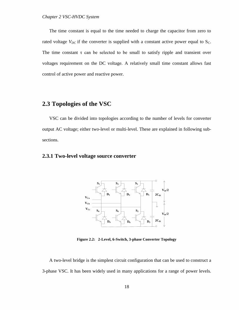
2.3.1 Two-level voltage source converter
Vdc/2
Vdc/2
VCa
VCb
VCc
2Cdc
2Cdc
S1 S3 S5
S4 S6 S2
D1 D3 D5
D4 D6 D2
Figure 2.2: 2-Level, 6-Switch, 3-phase Converter Topology
A two-level bridge is the simplest circuit configuration that can be used to construct a
3-phase VSC. It has been widely used in many applications for a range of power levels.

Chapter 2 VSC-HVDC System
19
As shown in Fig. 2.2, the converter can generate DC voltage waveform of only two
values, ±Vdc/2, where Vdc is the total DC voltage. Relatively simple power and control
circuitry, small DC capacitor size, small foot print environmentally and same semi
conductor duty ratio, are some of the advantages related to a two-level VSC.
2.3.2 Multi-level voltage source converter
Converters topologies with more than 2-level voltages are known as multilevel
converters. In this type of VSC, the output AC voltage waveform has different level
according to the construction of the VSC. The main requirement for multilevel converter
is to synthesize a sinusoidal voltage from several voltage levels which are obtained from
the DC side capacitor voltages. Multilevel VSCs are divided into different types
according to their application. The multilevel VSC found various applications in power
systems due to its high power density, excellent performance and high reliability. Various
multi-level topologies are explained next.
2.3.2.1 Neutral point diode clamped VSC
Neutral point diode clamped VSC topology is shown in Fig. 2.3. As shown, this
topology uses clamping diodes to limit the dynamic and static over voltages of switching
devices. The clamping diodes are connected to the centre point of the DC bus capacitor.
The advantages of this topology include reasonable small size of the DC capacitors,
small foot print environmentally and good quality AC output waveform. An n-level
diode-clamp converter typically consists of (n-1) capacitors on the DC bus and produces
n-levels of the converter output AC voltage. With a higher number of levels, harmonics
generation is very low which can even avoid the need for filters in some cases. The
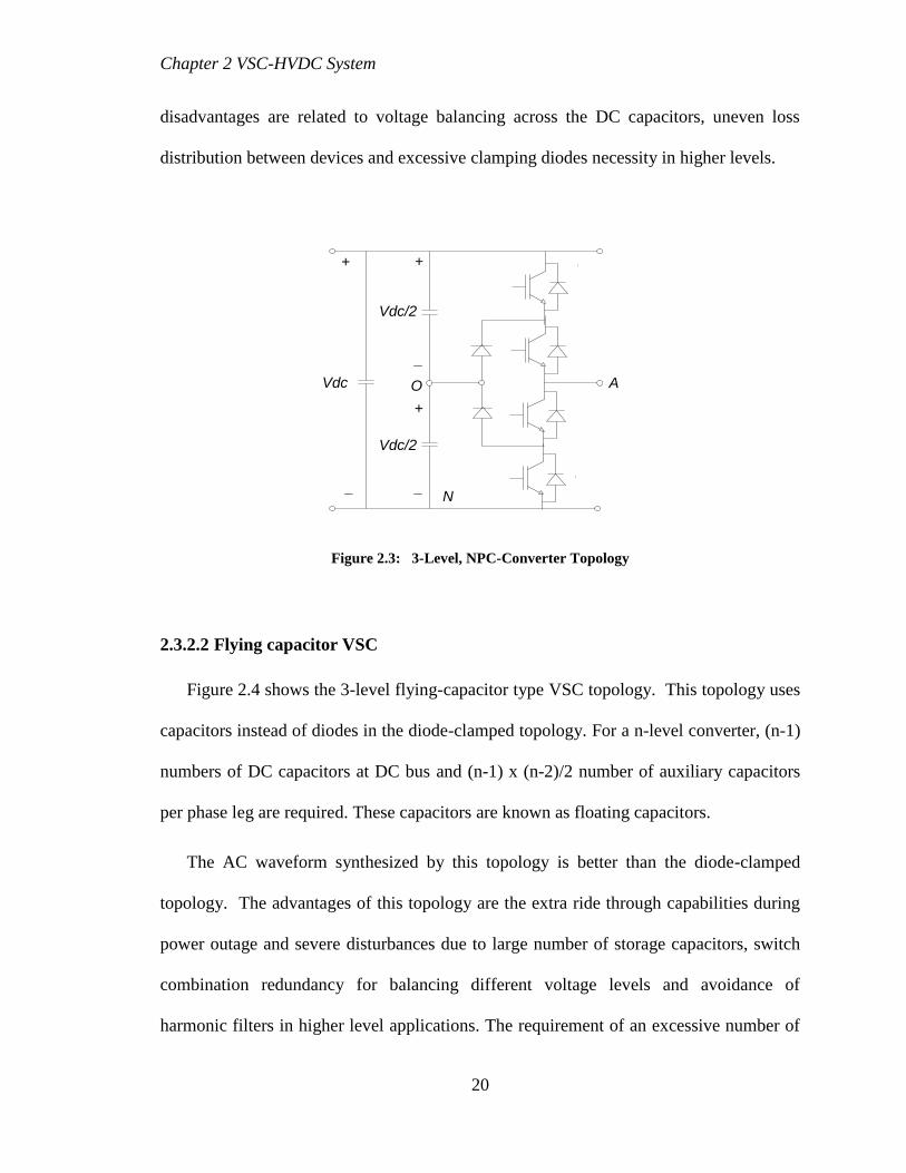
Chapter 2 VSC-HVDC System
20
disadvantages are related to voltage balancing across the DC capacitors, uneven loss
distribution between devices and excessive clamping diodes necessity in higher levels.
N
Vdc/2
Vdc/2
Vdc A
++
+
__
_
O
Figure 2.3: 3-Level, NPC-Converter Topology
2.3.2.2 Flying capacitor VSC
Figure 2.4 shows the 3-level flying-capacitor type VSC topology. This topology uses
capacitors instead of diodes in the diode-clamped topology. For a n-level converter, (n-1)
numbers of DC capacitors at DC bus and (n-1) x (n-2)/2 number of auxiliary capacitors
per phase leg are required. These capacitors are known as floating capacitors.
The AC waveform synthesized by this topology is better than the diode-clamped
topology. The advantages of this topology are the extra ride through capabilities during
power outage and severe disturbances due to large number of storage capacitors, switch
combination redundancy for balancing different voltage levels and avoidance of
harmonic filters in higher level applications. The requirement of an excessive number of

Chapter 2 VSC-HVDC System
21
storage capacitors on DC side and across the semi-conductor switches in higher number
of levels makes this topology very expensive. The converter control system is complex
and switching losses are higher compared to diode clamped topology.
N
Vdc/2
Vdc/2
Vdc A
+
+
_
_
CfVdc/2
+
_
O
Figure 2.4: 3-Level, Flying Capacitor Converter Topology
2.3.2.3 ANPC (Actively Neutral Point Clamped) converter
Figure 2.5 shows the 3-level ANPC converter topology in which the clamping diodes
are replaced by semi-conductor switches. The disadvantage of uneven loss distribution
across various devices in the neutral point diode clamped converter topology is mitigated
by this newly developed topology.

Chapter 2 VSC-HVDC System
22
N
Vdc/2
Vdc/2
VdcA
+
+
+
_
_
_
O
Figure 2.5: 3-Level, Actively Neutral Point Clamped Converter Topology
2.3.2.4 Cascaded H-bridge converter
This VSC topology (Fig. 2.6) is a cascaded structure consists of full bridge inverter
units connected in series.
Vdc/4
Vdc/4N
Figure 2.6: 5-Level, Cascaded H-bridge Converter Topology

Chapter 2 VSC-HVDC System
23
Each unit is fed by a separate DC capacitor and no other circuit to balance the voltage
matching of the switching devices is necessary. There is no need to add the clamping
diodes or voltage balancing capacitors in this topology which results in a relatively
simple construction. Main drawback of this topology is the requirement of several
independent DC power supplies.
2.3.3 Multi-pulse topologies
In a 6-switch converter, the commutation of current takes place six times per cycle. In
case of 12-switch converter, two six-switch converters are connected in series to form a
twelve-switch converter topology. By using the 6-switch converter, the additional multi-
switch topologies in multiples of six can be created to form the required pulse-level. The
24-switch and 48-pulse converters are implemented in some research papers for
application as a STATCOM in power system. The main purpose of using these topologies
is to reduce the voltage and current harmonics in the system. As the number of switches
increases the harmonic distortion in the system decreases proportionally.
Chapter 2 VSC-HVDC System
24
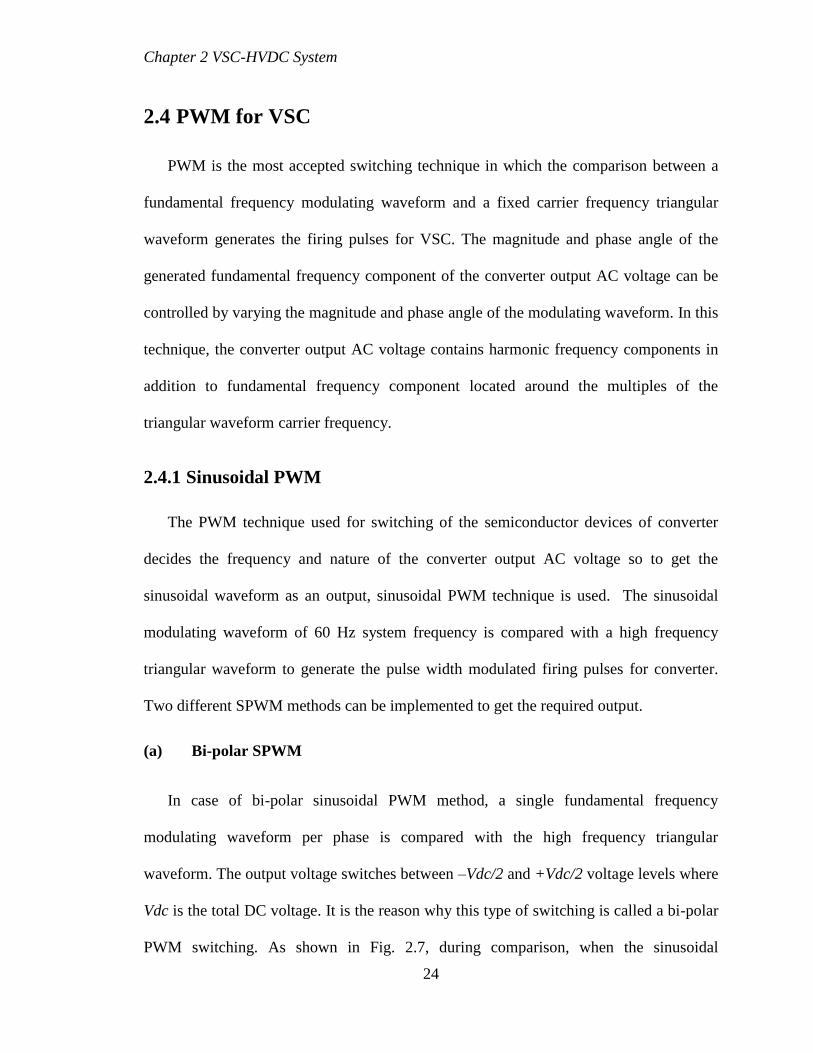
2.4 PWM for VSC
PWM is the most accepted switching technique in which the comparison between a
fundamental frequency modulating waveform and a fixed carrier frequency triangular
waveform generates the firing pulses for VSC. The magnitude and phase angle of the
generated fundamental frequency component of the converter output AC voltage can be
controlled by varying the magnitude and phase angle of the modulating waveform. In this
technique, the converter output AC voltage contains harmonic frequency components in
addition to fundamental frequency component located around the multiples of the
triangular waveform carrier frequency.
2.4.1 Sinusoidal PWM
The PWM technique used for switching of the semiconductor devices of converter
decides the frequency and nature of the converter output AC voltage so to get the
sinusoidal waveform as an output, sinusoidal PWM technique is used. The sinusoidal
modulating waveform of 60 Hz system frequency is compared with a high frequency
triangular waveform to generate the pulse width modulated firing pulses for converter.
Two different SPWM methods can be implemented to get the required output.
(a) Bi-polar SPWM
In case of bi-polar sinusoidal PWM method, a single fundamental frequency
modulating waveform per phase is compared with the high frequency triangular
waveform. The output voltage switches between –Vdc/2 and +Vdc/2 voltage levels where
Vdc is the total DC voltage. It is the reason why this type of switching is called a bi-polar
PWM switching. As shown in Fig. 2.7, during comparison, when the sinusoidal

Chapter 2 VSC-HVDC System
25
waveform is greater than the triangular waveform, the PWM trigger signal is high;
otherwise at lower level.
Figure 2.7: Comparison between Sinusoidal and Triangular waveform and PWM Signals
(b) Uni-polar SPWM
In case of uni-polar sinusoidal PWM technique, two same phase fundamental
frequency modulating waveforms with opposite polarity are compared with the high
switching frequency triangular waveforms. The output voltage switches between +Vdc/2
and zero or between zero and –Vdc/2. For this reason, this type of PWM scheme is called
a PWM with a uni-polar voltage switching.

Chapter 2 VSC-HVDC System
26
2.5 VSC-HVDC Operation
The VSC-HVDC operation can be explained by considering its operating principle,
four-quadrant operation in PQ-diagram and capability to operate in either rectifier or
inverter modes.
2.5.1 Operating principle of VSC-HVDC
The VSC-HVDC operating principle can be explained from the SLD shown in Fig.
2.8, where two AC networks are connected by a VSC-HVDC transmission system.
AC
ACDC
DC
Sending end
Converter-1
Receiving end
Converter-2
Vs1 /_0 Vc1 /_δ1 Vs2 /_0Vc2 /_δ2
VDC
AC system AC systemTransformer Transformer
XT1 XT2
Figure 2.8: Single Line Diagram for VSC-HVDC Operating Principle
The converter transformer connecting AC network and converter can be modeled as
an equivalent series resistance and reactance. The transformer resistance is very small
compared to the transformer reactance so it can be neglected in power calculations. The
phase shift between both sides’ voltages due to transformer reactance is responsible for
active power flow. At sending end, the voltage VS1 at AC bus is considered as a reference
so the converter output AC voltage VC1 has phase shift δ1 with respect to the bus voltage
VS1. The magnitude and phase angle of converter output AC voltage VC1 is controlled by

Chapter 2 VSC-HVDC System
27
the VSC control system. The active and reactive power flow between the AC system and
the converter depends on the magnitude of the voltages at both sides of the transformer,
the transformer reactance and the phase angle δ1 between them. The active and
reactive power flow between AC bus and converter AC terminals can be expressed as
follows:
The active power at sending end and receiving end is given by,
(2.1)
The reactive power at sending end and receiving end is given by,
(2.2)
The amplitude, phase angle and frequency of fundamental component of converter
output AC voltage VC1 and VC2 can be controlled using the SPWM technique. If the
voltage at the DC side of the converter is VDC which is assumed to be constant then the
fundamental frequency component of converter output AC voltage can be derived from
the following equation:
(2.3)
Where VDC is the voltage on DC side, ω is the angular frequency, Mi is modulation
index and δ is the phase angle between the converter output AC voltage and the AC bus
voltage.
Mi can be defined as the ratio of peak value of voltage of modulating waveform
(fundamental frequency sinusoidal waveform) to the peak value of voltage of carrier
waveform (switching frequency triangular waveform). From Eqn. 2.3, it is seen that the

Chapter 2 VSC-HVDC System
28
fundamental component of converter voltage depends on the variables Mi, angle δ and
frequency which are independently controlled by VSC controllers. The active and
reactive power can be controlled by controlling the phase angle δ and the amplitude of
the fundamental frequency component of converter AC output voltage VC respectively.
In a VSC-HVDC, the polarity of DC voltage is constant so the power reversal is done
by current reversal in the DC link. The current in DC link flows from higher to lower DC
voltage level. For stable VSC operation and flow of active power, the DC link voltage is
maintained at a desired reference value by using a feedback control loop. The power flow
to and from the AC source can be controlled according to the DC link voltage
requirements. The voltage VDC is measured and controlled in such manner that the DC
current flow can be in either direction depending on the requirement of active power flow
direction.
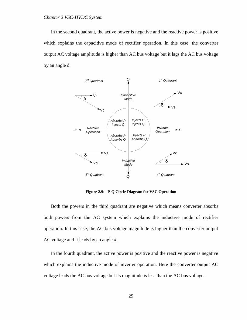
2.5.2 Four quadrant operation of VSC
Active power flow direction for rectifier or inverter operation and reactive power
flow direction for inductive or capacitive operating mode of VSC can be explained by a
PQ-circle diagram shown in the Fig. 2.9. The diagram explains the ability of VSC to
operate in all four quadrants of PQ-circle and to achieve the independent control of active
and reactive power. The direction of current flow and hence active power flow decides
the rectifier or inverter operation of converter.
In the first quadrant both the active and reactive power are positive which means that
the converter injects both powers to AC system which shows the capacitive mode of
inverter operation. The converter output AC voltage magnitude is higher than AC bus
voltage and leads AC bus voltage by an angle δ.
Chapter 2 VSC-HVDC System
29
In the second quadrant, the active power is negative and the reactive power is positive
which explains the capacitive mode of rectifier operation. In this case, the converter
output AC voltage amplitude is higher than AC bus voltage but it lags the AC bus voltage
by an angle δ.
Inverter
OperationRectifier
Operation
Capacitive
Mode
Inductive
Mode
Injects P
Injects QAbsorbs P
Injects Q
Absorbs P
Absorbs Q
Injects P
Absorbs Q
δ
δVs
Vc Vs
Vc
δVs
Vc δVs
Vc
P-P
Q
-Q
1st Quadrant2
nd Quadrant
3rd
Quadrant 4th Quadrant
Figure 2.9: P-Q Circle Diagram for VSC Operation
Both the powers in the third quadrant are negative which means converter absorbs
both powers from the AC system which explains the inductive mode of rectifier
operation. In this case, the AC bus voltage magnitude is higher than the converter output
AC voltage and it leads by an angle δ.
In the fourth quadrant, the active power is positive and the reactive power is negative
which explains the inductive mode of inverter operation. Here the converter output AC
voltage leads the AC bus voltage but its magnitude is less than the AC bus voltage.
Chapter 2 VSC-HVDC System
30
According to the converter MVA capacity and system requirements, converter can
operate in any mode (i.e. capacitive or inductive) of rectifier or inverter operation.
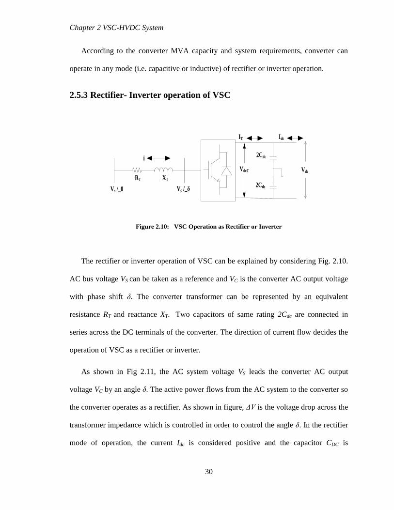
2.5.3 Rectifier- Inverter operation of VSC
Vdc
Vs /_0 Vc /_δ
RT XT
2Cdc
2Cdc
i
IT Idc
VdcT
Figure 2.10: VSC Operation as Rectifier or Inverter
The rectifier or inverter operation of VSC can be explained by considering Fig. 2.10.
AC bus voltage VS can be taken as a reference and VC is the converter AC output voltage
with phase shift δ. The converter transformer can be represented by an equivalent
resistance RT and reactance XT. Two capacitors of same rating 2Cdc are connected in
series across the DC terminals of the converter. The direction of current flow decides the
operation of VSC as a rectifier or inverter.
As shown in Fig 2.11, the AC system voltage VS leads the converter AC output
voltage VC by an angle δ. The active power flows from the AC system to the converter so
the converter operates as a rectifier. As shown in figure, ΔV is the voltage drop across the
transformer impedance which is controlled in order to control the angle δ. In the rectifier
mode of operation, the current Idc is considered positive and the capacitor CDC is

Chapter 2 VSC-HVDC System
31
discharged through the DC transmission system. The error signal demands the control
circuit for more power from the AC supply. The control circuit thereby generating the
appropriate PWM signals for the switching devices and accordingly, more current flows
from the AC to DC side and the capacitor voltage recovers its predefined value.
Vs
Vc
δ
I
ΔV
Re
Im
Figure 2.11: VSC Operation as a Rectifier
As shown in Fig 2.12, the AC system voltage VS lags the converter AC output
voltage by an angle δ. In this case, the active power flows from the converter to AC
system so the converter operates as an inverter. In the inverter mode of operation, Idc
becomes negative and the capacitor CDC is overcharged. The error signal demands the
controls to discharge the capacitor CDC and return power to the AC system. The PWM
can control both the active power and reactive power independently. Thus, this type of
converter can be used for power factor correction also in addition to power transmission.

Chapter 2 VSC-HVDC System
32
Vs
Vc
δ
I
ΔV
Re
Im
Figure 2.12: VSC Operation as an Inverter
Depending on the control strategy, VSC can be operated as either inverter or rectifier;
therefore it is often referred to as a converter. Two such converters are often cascaded to
control the power flow between two AC networks. The first converter converts AC
voltage to variable DC link voltage and the second converter converts the DC voltage to
variable AC voltage with fixed or variable frequency.
2.6 Summary
In this chapter, the VSC-HVDC system construction, its principle of operation and
operational function of each component is explained in detail. The different topologies of
VSC and PWM techniques are explained. The principle of operation for the VSC-HVDC
is explained regarding the active and reactive power flow. PQ-circle diagrams are
explained regarding the rectifier/inverter operation and capacitive or inductive mode of
operation.

33
Chapter 3
Control of VSC-HVDC System
3.1 Introduction
VSC-HVDC transmission system has flexibility in terms of controlled quantities
offering two degrees of freedom at each end to provide stable and robust control. As
described in section 2.5, VSC-HVDC system has advantage of independent control of
active and reactive power. The direction of active power flow can be changed without
changing the DC voltage polarity. The reactive power can be controlled independently at
either converter station by controlling converter AC output voltage.
Although both current and voltage control schemes are possible, current control is
generally preferred for its excellent dynamic characteristics and inherent over-current
limitation capabilities. When current control is used, the rectifier input current and
inverter output currents are measured and compared with reference signals; the current
errors are used as inputs to the PWM modulator, which then provides the required
switching signals. The requirements for the control system to operate the VSC-HVDC
system are:
It must be capable of controlling the desired active power in either direction.
The reactive power of system must be controlled independently at both ends.
The DC voltage must be maintained at desired level for power transfer.

Chapter 3 Control of VSC-HVDC System
34
The control modes are chosen according to the application and requirement of the
given power system. The rectifier and inverter controllers take the control of any two of
above mentioned four control strategies according to the system requirements and
operating conditions. VSC1 controllers operate on active power and reactive power
control whereas VSC2 controllers deal with DC voltage and reactive power control (Fig.
3.1).
AC
ACDC
DC
AC Voltage /
Reactive power
Control
AC Voltage /
Reactive power
Control
Active Power
Control
DC Voltage
Control
Converter-1 Converter-2
AC System
Reactance Reactance
AC System
Figure 3.1: VSC-HVDC Control System
3.2 Direct control method
Direct control method is a simple method for the control of VSC-HVDC. The angle δ
and modulation index Mi are controlled directly by using PI controllers. The measured
values are compared with the reference values and the resultant errors are fed to the PI-
controllers. The output of which is used as either modulation index or angle delta. The
modeling of direct control system is provided in section 4.5.3. Though this method is not
used in practical applications, it is useful in comparative studies of operation and
performance of VSC-HVDC.

Chapter 3 Control of VSC-HVDC System
35
3.3 Vector control method
The P and Q controlled quantities of VSC-HVDC are coupled to each other such that
any change in one quantity strongly affects the other. The vector control method removes
the coupling between these quantities to ensure the independent control of each quantity.
The vector control strategy consists of a cascade control system with faster inner
controllers. The vector controller is accomplished by additional outer current controller
which provides the reference values for inner controller. The outer controllers include
active power controller, reactive power controller, AC voltage controller, DC voltage
controller or frequency controller where the implementation of particular control strategy
depends on the application and operating conditions of VSC-HVDC system. It is not
possible to implement all the control strategies at the same time and requires an extensive
system operation and performance studies for implementation of particular control
method.
For feeding the passive system at receiving end without any local voltage source, it is
necessary to control the frequency and AC voltage whereas the active power and reactive
power control is required in active AC system. However, since the active power flow into
the DC link must be balanced, the DC voltage controller is necessary in any case to
achieve active power balance. On the DC side, the active power input to the DC link must
equal the active power output from the DC link plus the losses in the DC link. Any
difference would result in a change in the DC voltage.
In order to understand the vector control technique of the VSC-HVDC transmission
system, the mathematical model for VSC-HVDC system needs to be derived. The vector
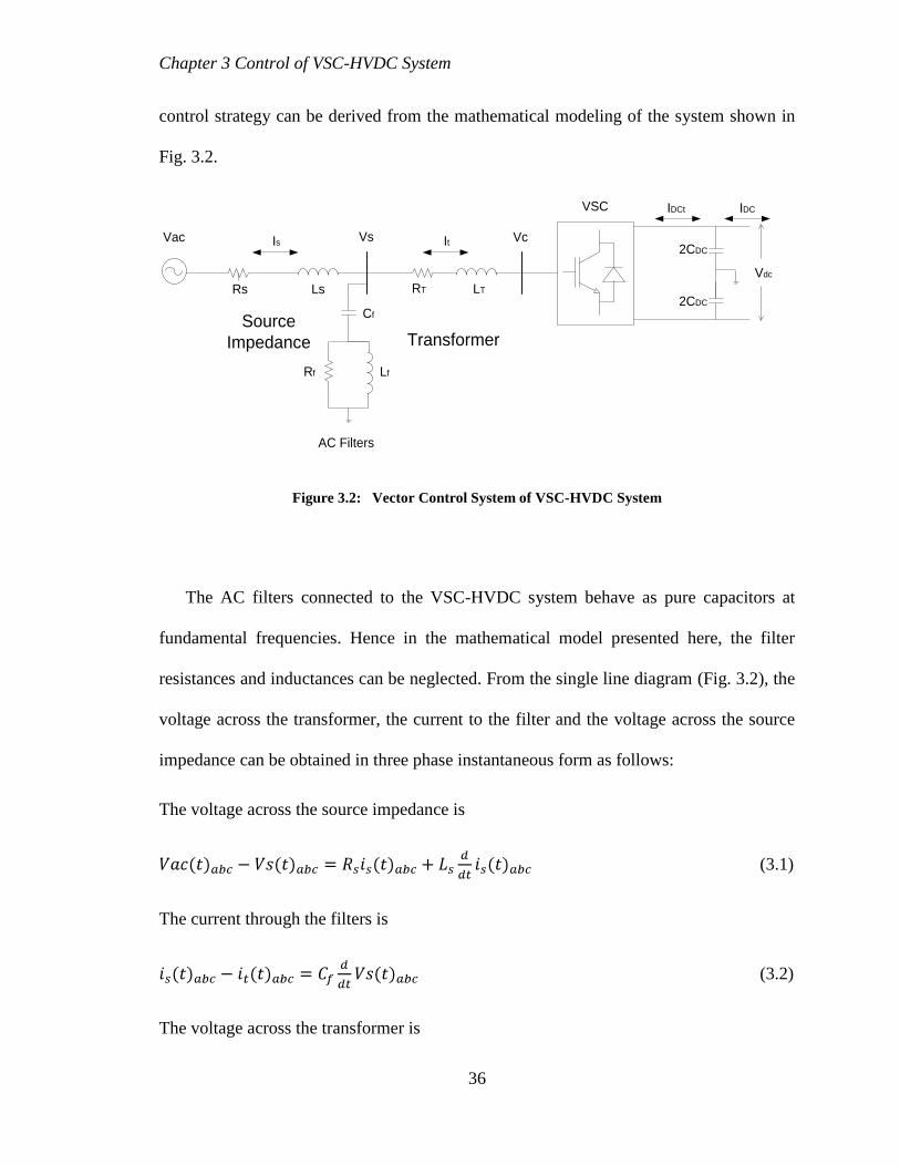
Chapter 3 Control of VSC-HVDC System
36
control strategy can be derived from the mathematical modeling of the system shown in
Fig. 3.2.
Vdc
Vs Vc
RT LT
Vac
Ls
VSC
2CDC
2CDC
AC Filters
Rf Lf
Cf
It
Rs
Is
IDCt IDC
TransformerSource
Impedance
Figure 3.2: Vector Control System of VSC-HVDC System
The AC filters connected to the VSC-HVDC system behave as pure capacitors at
fundamental frequencies. Hence in the mathematical model presented here, the filter
resistances and inductances can be neglected. From the single line diagram (Fig. 3.2), the
voltage across the transformer, the current to the filter and the voltage across the source
impedance can be obtained in three phase instantaneous form as follows:
The voltage across the source impedance is
(3.1)
The current through the filters is
(3.2)
The voltage across the transformer is

Chapter 3 Control of VSC-HVDC System
37
(3.3)
From (3.1), (3.2) and (3.3), the following differential equations can be derived:
(3.4)
(3.5)
(3.6)
By using Clark’s transformation matrix (Appendix C), quantities from ABC-frame can be
converted to αβ-reference frame as follows,
(3.7)
Where γ=2π/3.
Equations (3.4), (3.5) and (3.6) can be converted in to αβ frame as follows:
(3.8)
(3.9)
(3.10)
By using the transformation angle Ө derived from a phase-locked loop (PLL), the above
equations are further transferred to the synchronously rotating dq-reference frame, using
Park’s transformation, as follows:
Chapter 3 Control of VSC-HVDC System
38
(3.11)
(3.12)
(3.13)
(3.14)
The AC filter voltage, the current through the transformer and the AC side voltage of
VSC can be expressed as:
(3.15)
(3.16)
(3.17)
From equation (3.17), the dq-current component through the transformer can be given as,
(3.18)
(3.19)
Equations (3.18) and (3.19) present the relationship between input reference current and
the converter output AC voltage in dq-reference frame.

Chapter 3 Control of VSC-HVDC System
39
3.4 Limitations
The VSC-HVDC link with its semi-conductor switches has a limited overload
capacity. Large transient currents due to system disturbances can stress or damage the
converter valves. Therefore, a current limit must be implemented in the control system.
Moreover, since the maximum voltage amplitude out of the VSC is limited by the VSC
voltage capability, the produced reference voltage from the vector controller must be
appropriately limited. The current limit Ilim is compared with the current magnitude
computed from the active and reactive reference currents. When the current limit is
exceeded, both the active and reactive reference currents have to be limited. The choice
of how to limit both reference currents will depend on the application. For instance, if the
converter is connected to a strong system, the active component of the reference current
will be given priority, when the current limit is exceeded, to produce more active power.
The produced active power is estimated from the equation
(3.20)
If the converter is connected to a weak system or used to supply a bulk industrial user
(or island), the VSC will give priority to the reactive component of the reference current
to maintain the AC voltage when the current limit is exceeded. The remaining capacity is
then available for active power production. The produced reactive and active power may
be estimated from the following equations:
, (3.21)
Where, is the pre-set maximum reactive reference current.
Chapter 3 Control of VSC-HVDC System
40
3.5 Outer controller
The outer controller consists of the DC voltage controller, active power controller and
reactive power controller. The proposed simulation model consists of active power and
reactive power controllers at VSC1 and DC voltage and reactive power controllers at
VSC2. The outer controller creates the reference values of the dq-current components for
inner current controllers. The outer controller gains are smaller when compared to the
inner controller to ensure the stability of the complete system.
3.5.1 DC voltage controller
As shown in the Fig. 3.2, the instantaneous active and reactive powers in dq-reference
frame at the AC side of the VSC and the power PDC transmitted on the DC side of the
VSC are expressed as:
(3.22)
(3.23)
(3.24)
Where, is the current flowing in the DC terminals of the VSC.
During steady state operation, the dq-components of voltages are constant at the rated
values. Therefore, the voltage is rated voltage VS and is zero. By considering the
above assumptions, the active and reactive powers are expressed as follows:
(3.25)

Chapter 3 Control of VSC-HVDC System
41
If the losses in the converter trasformer and converter are neglected, the power at the AC
and DC sides can be considered equal, i.e.
(3.26)
Hence,
(3.27)
The current in the DC line of the VSC is given as:
(3.28)
Any imbalance between the AC and DC powers leads to a change in voltage at the DC
link capacitors, which is given as:
(3.29)
Where, is the current in the DC terminals of the VSC, is the total DC side
capacitance, VDC is the DC voltage across the capacitor and IDC is the DC current flowing
through the transmission line. The value of DC current from equation (3.28) can be used
in equation (3.26), i.e.
(3.30)
(3.31)
From equation (3.30), the value of the reference current id *
is derived as follows:

Chapter 3 Control of VSC-HVDC System
42
(3.32)
The d-component of the current derived in the equation (3.32) gives the reference current
for the inner current controller for DC voltage control.
3.5.2 Active power controller
The active current reference is obtained from equation (3.25)
(3.33)
Where, Pref is the reference active power. For accurate control of the active power, a
combination of a feedback loop and an open loop is used.
(3.34)
Where, Kp1 and Ki1 are the proportional and integral gains respectively of the active
power controller.
3.5.3 Reactive power controller
A reactive power controller similar to the active power controller is obtained from
equation (3.25) as:
(3.35)
Where, Qref is reference reactive power. Again, same method is used to combine a
feedback loop with an open loop,
(3.36)
Chapter 3 Control of VSC-HVDC System
43
Where, Kp2 and Ki2 are the proportional and integral gains respectively of the reactive
power controller.
Fig. 3.3 shows active and reactive power control system for VSC1. The control block of
PLL is shown from which the synchronization angle Ө is derived and fed to the ABC to
dq block.

Chapter 3 Control of VSC-HVDC System
44
PI1 PI2Pref
Pmeas Id meas
ωLIq
Vsd
Vcd+++ __
PI3 PI4Qref
Qmeas Iq meas
ωLId
Vsq
_+++ __
dc
cqcd
V
VVM
222
cd
cq
V
V1tan
Sinusoidal
PWM
Vdc
Firing
Pulses
Outer Current Control Loop Inner Current Control Loop
Inner Current Control Loop
PLL θVsaVsbVsc
abc
dq
VsaVsbVsc
Vsd
Vsq
θSynchronization Block
Vcq
Outer Current Control Loop
+
_
+
Figure 3.3: Active and Reactive Power Control System
Chapter 3 Control of VSC-HVDC System
45
3.6 Summary
This chapter deals with the control system of VSC-HVDC transmission system. Two
different control systems, direct control and vector control are explained. The VSC-
HVDC mathematical model is provided in this chapter. Block diagram of active power
and reactive power control systems in vector control technique is also provided here.

46
Chapter 4
Methodology
4.1 Introduction
For simulation of the provided VSC-HVDC system, it is necessary to model each and
every component in a realistic manner which can then provide a clearer understanding of
the actual system behaviour. The different components of the system are modeled in
EMTP-RV package. The parameters of voltage sources, filters, transformers, DC
capacitors and overhead DC cables are provided. The complete model of the VSC-HVDC
transmission system can be divided in the following different blocks which are connected
to each other.
4.2 Power system modeling
The power system components such as transformers, filters, VSC, DC capacitors and
DC overhead cables are integrated in VSC-HVDC model (Fig. 2.1). The necessary
calculations to convert the system data and equipment ratings to per unit (pu) values are
provided in Appendix A. The simulated measuring instruments of the software package
are calibrated using these per unit calculations to measure system values.
Chapter 4 Methodology
47
4.2.1 Modeling of weak AC networks
Two, 230 kV (RMS L-L), 100 MVA weak AC networks with Short circuit ratio
(SCR) of 3 are connected through a VSC-HVDC link. A source impedance of 176.05 Ω
is connected at both ends to present the SCR of 3. The weak AC systems presented here
are balanced 3-phase sources at a fixed frequency of 60 Hz.
4.2.2 Modeling of converter transformer
Converter transformer reactance works as a necessary element for power transfer
between AC and DC systems. The transformer configuration used here is a star ground-
star (Yg-Y) which avoids the phase shifting between primary and secondary voltages.
The rating of the converter transformer is 115 MVA, 230 kV primary voltage and 49 kV
secondary voltage (230/49 kV), 60 Hz. The rated DC voltage of ± 40 kV is chosen for
VSC-HVDC which results in the 49 kV (RMS L-L) as a converter transformer secondary
voltage. The rated per unit resistance is Rpu= 0.00375 pu and the reactance is Xpu= 0.12
pu. The resistance of transformer is very small compared to reactance so it is neglected in
power calculations.
The transformer is operating in the linear range and operation under saturation is not
considered. The aforementioned configuration is shown in Fig. 4.1 where three single
phase units are connected in star configuration at primary and secondary sides.

Chapter 4 Methodology
48
Figure 4.1: Converter Transformer Model
4.2.3 Modeling of AC shunt RLC-Filters
The order of harmonics generated by the switching action of the semiconductor
devices of converter depends on the switching frequency and configuration of the
converter. The single-tuned low-pass and high-pass damped RLC filters are connected in
parallel at appropriate location(s) in AC system to mitigate the harmonics. The low-pass
filters are modeled as a series connected RLC branch and high-pass damped filters are
modeled by parallel combination of resistance and inductance connected in series with
the capacitor.
3 identical non-ideal units
YY transformer
inY outY
NeutralW1 NeutralW2
+
xfmr_YY_unitO
xfmr_A
+
xfmr_YY_unitO
xfmr_C
+
xfmr_YY_unitO
xfmr_B
Y
b
a
c
NW2NW1
Yout
b
a
c

Chapter 4 Methodology
49
Figure 4.2: EMTP-RV Filter Modeling and Frequency Scan graph
4th, 5 MVA
5th, 5 MVA
7th, 5MVA
8th, 5 MVA
High pass filtertuned to 6 th25 MVA
High pass filtertuned to 17 th 25 MVA
FILTERS
+
5.51,0.4385,0.25072uF
+
14.11,1.1226,0.251uF
+
29.385
+
1.5uF
+
22.05,1.754,0.25072uF
+
2.91,0.24,0.25072uF
+
0.1871
+
3
+
1.5uF
+
0.0223117

Chapter 4 Methodology
50
The 4th
, 5th
, 7th
and 8th
harmonic frequency low-pass tuned filters and 6th
and 17th
harmonic frequency high-pass damped filters are connected in parallel to make a single
filter unit (Fig. 4.2). The rating of any particular harmonic frequency filter is decided
using the value of that particular (voltage and current) harmonic content. The frequency
scan graph for the filter is also provided in Fig. 4.2, which shows the least impedance for
the particular harmonic frequency component. In case of VSC-HVDC system, the
reactive power compensation is less important due to the capability of VSC to operate as
a reactive power compensator which results in smaller size of the capacitor required for
the filters. As explained earlier, the harmonics in VSC-HVDC are multiples of the
switching frequency of the semiconductor valves so the high-pass damped filters are
required to eliminate these harmonics. The necessary calculations for the filter design are
provided in APPENDIX-B. The filters of 70 MVAR in total are connected at high
voltage side of the transformer and the individual filter ratings are provided in Table 4.1.
The MATLAB code for filter RLC-parameters calculations and values of RLC-
parameters are provided in Appendix B.
Table 4-1 Filter Ratings
Filters at VSC1 Filters at VSC2
Harmonic Order Rating (MVAR) Harmonic Order Rating (MVAR)
4th
5 4th
5
5th
5 5th
5
7th
5 7th
5
8th
5 8th
5
6th
50 6th
25
17th
0 17th
25

Chapter 4 Methodology
51
4.3 Converter Modeling (Rectifier and Inverter)
The converters are most important components of VSC-HVDC system since they
convert AC voltage into DC voltage and vice versa. The converters are composed of
number of devices such as semi conductor switches, diodes, RC snubbers and resistances
and inductances.
4.3.1 Converter topology modeling
The 3-phase, 2-level, and 6-switch VSC topology is implemented for this model. The
output voltage of the converter can have only two levels; –VDC/2 and + VDC /2 where VDC
is the total DC voltage between two DC poles. The modeling of high-power high-
frequency switching device is done by using an ideal controlled switch. This semi-
conductor switch connected with anti-parallel diode make one unit. In actual installation,
there are several units connected in series to get the required voltage level. In this
simulation model, only one unit is used to study the operational performance of the
converter. The voltage pulses generated by SPWM technique in control system are the
firing signals for these switches.
The units are connected in the order of predetermined firing sequence. The units 1
and 4 are connected to phase A, units 3 and 6 are connected to phase B and units 2 and 5
are connected to phase C. As shown in Fig. 4.3, the firing of the switches in the same
phase is complementary to prevent the risk of the short circuit across the DC terminals of
the converter. Therefore, a finite blanking time of a few nano-seconds is added to each
firing signal to achieve some degree of protection. In ideal case, it is considered that all
the switches are ideal without any kind of time delay so no blanking time is added to the

Chapter 4 Methodology
52
firing signals generated in this simulation. RL-snubbers are connected in DC terminals to
provide di/dt limitation for the converters.
Figure 4.3: Converter Model in EMTP-RV
4.3.2 IGBT-Diode module modeling
The IGBT-Diode unit is modeled as shown in Fig.4.4 where the controlled switch is
represented by an ideal switch. The diode is also considered as an ideal element so on-
state losses and switching losses are neglected. The anti-parallel diode operates in the
complementary manner with the IGBT which makes the converter a bi-directional
operating device. As explained earlier in section 2.5.1, the converter can operate in all
four quadrants of V-I plane so the direction of current flow must be bi-directional. The
diode connected in series with IGBT switch serves the purpose of protection due to IGBT
switch being a unidirectional device where the current cannot flow in opposite direction.
firing
Pc
Pb
Pa
DC2
+
1k
P
P2
P1
1
P
P2
P1
3
P
P2
P1
5
P
P2
P1
4
P
P2
P1
6
P
P2
P1
2
+
1mH
+
1mH
+
1k
f1f2f3f4f5f6
DC1
firing

Chapter 4 Methodology
53
Each unit is equipped with a RC snubber connected across the switch and the diode in
order to reduce the rate of change of voltage (dv/dt) during the switching of the semi
conductor devices. The switching frequency of converter is 1440 Hz which results in 24
ON-OFF operations per cycle.
Figure 4.4: IGBT Valve Modeling
In actual installations, during each process of switching from one state to another
state, there is a power loss in the switching device which is directly related to the
DC TERMINAL
AC TERMINALP1
P2
+
1.5uF
0.7
0
+
16k
+
0.0
1m
H
+
0.0
1m
H
+
0.0
0001
P
+
1.5uF
0.7
0
+
+
1.5uF
+
16k+
16k
+
0.0
000000001
+
0.0
000000001
Chapter 4 Methodology
54
switching frequency. During the switching action, the rate of change of voltage and
current is very high which can expose the device to failure so the RC snubber circuit in
parallel with semiconductor device is employed for protection. The optimized RC
snubbers reduce the stress on the switching devices by limiting the voltage stresses at turn
ON and turn OFF. The series resistance and inductors also reduce the rate of change of
current stresses (di/dt) in the semiconductor devices. The rating of the RC snubber is
estimated from the system parameters like voltage and current rating of the devices and
the total amount of power loss through the valve.
4.4 DC capacitors and transmission system modeling
DC capacitors are connected across the DC terminals of the VSC to maintain the DC
voltage required for the dynamics of the system. The PWM switching of converter
creates the harmonics in the current flowing in DC transmission system. This current
generates ripple in the DC voltage; magnitude of which depends on the DC capacitor size
and converter switching frequency. The rating of capacitor is decided according to the
DC voltage level and the rating of VSC. Two capacitors of 400 µF are connected in
cascade form with the common terminal grounded. An identical DC capacitor is used at
both ends of the DC system.
The DC system can be in the form of overhead transmission line, underground DC
cables or overhead DC cables. DC transmission line is modeled in the same way as an
AC transmission line. The bi-polar transmission system is implemented here with a
grounded midpoint providing the return path during monopolar operation. The power can

Chapter 4 Methodology
55
still be transmitted by one pole in case of failure or scheduled maintenance of other pole
in actual systems. The model presented here is based on the overhead DC cables of 75
km length; divided into three T-sections of 25 km on each pole (Fig 4.5).
Figure 4.5: DC Transmission System Modeling
The resistance, inductance and capacitance of the DC cable are calculated from the
data collected for the per unit length of cable. The DC system used here is a bi-polar
transmission system so two identical cables are considered for positive and negative
poles. The RLC-parameters per unit length are provided in Table 4-2.
Table 4-2 DC Cable RLC-Parameters
Parameters Values per km Total Value
Resistance RDC 0.013 Ω/ km 1 Ω
Inductance LDC 0.16 mH/ km 12 mH
Capacitance CDC -- 100 µF
p1
p2
p3
p4
+
0.25
+
3mH
+
0.25
+
0.25
+
3mH
+
0.25
+
33uF
+
33uF
+
0.25
+
3mH
+
0.25
+
3mH
+
33uF
+
33uF
+
0.25
+
3mH
+
0.25
+
3mH
+
33uF
+
33uF
+
3mH
+
3mH
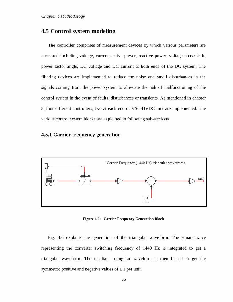
Chapter 4 Methodology
56
4.5 Control system modeling
The controller comprises of measurement devices by which various parameters are
measured including voltage, current, active power, reactive power, voltage phase shift,
power factor angle, DC voltage and DC current at both ends of the DC system. The
filtering devices are implemented to reduce the noise and small disturbances in the
signals coming from the power system to alleviate the risk of malfunctioning of the
control system in the event of faults, disturbances or transients. As mentioned in chapter
3, four different controllers, two at each end of VSC-HVDC link are implemented. The
various control system blocks are explained in following sub-sections.
4.5.1 Carrier frequency generation
Figure 4.6: Carrier Frequency Generation Block
Fig. 4.6 explains the generation of the triangular waveform. The square wave
representing the converter switching frequency of 1440 Hz is integrated to get a
triangular waveform. The resultant triangular waveform is then biased to get the
symmetric positive and negative values of ± 1 per unit.
Carrier Frequency (1440 Hz) triangular wavefroms
step
rc rv
++
-
c1.035
c
0
1
2
1440

Chapter 4 Methodology
57
4.5.2 Sinusoidal pulse width modulation (SPWM)
As explained in section 2.4, bi-polar SPWM method is implemented in this model.
The modulation index Mi is defined as,
(4.2)
Where, is peak amplitude of the fundamental frequency modulating waveform
and is the peak amplitude of the switching frequency triangular waveform.
The VSC output AC voltage should be sinusoidal with controlled magnitude, phase
angle and frequency. The sinusoidal modulating waveform at 60 Hz frequency is
multiplied with the modulation index Mi which results in changed amplitude according to
the value of modulation index. This resultant waveform is compared with the 1440 Hz
frequency triangular waveform to generate the firing pulses for the converter (Fig. 4.7).
The frequency of triangular waveform establishes the converter switching frequency
which is kept constant. Three, 120 degree phase shifted waveforms (a, b and c in Fig 4.7)
are compared with triangular waveform to get three 120 degree phase shifted firing
pulses for 3-phase legs of the converter. Each firing pulse is then extrapolated into two
complementary firing pulses to operate two switches in the same phase leg.

Chapter 4 Methodology
58
Figure 4.7: SPWM Block
4.5.3 Direct Control system modeling
As explained in section 3.2, the direct control system modeling is provided in this
sub-section. On the sending end, active power and AC filter bus voltage at VSC1 are
controlled whereas at receiving end side, DC voltage and AC filter bus voltage at VSC2
are controlled.
4.5.3.1 Angle delta block
The delta block comprises of 3-phase sinusoidal waveform generator which generates
three 120 degree phase shifted unitized sine waves (sin0, sin1, sin2 in Fig. 4.8). The angle
delta derived from the active power or DC voltage controller is added to the phase angle
Carrier Frequency(1440 Hz) triangular wavefroms
Sinusoidal Modulating signals
Firing Pulses to the Converter
Modulation Index
Compare
21
PROD
1
2
PROD1
2
PROD1
2
a
b
c
p4
p1
Compare
21
Compare
21
p6
p30
1
p2
p50
1
0
1
-1
-1
-1
0
1
0
1
mi
0
1
steprc rv
++
-
c
1.035
c0
1
2
1.5
0.6
11440
1440
1440
1440
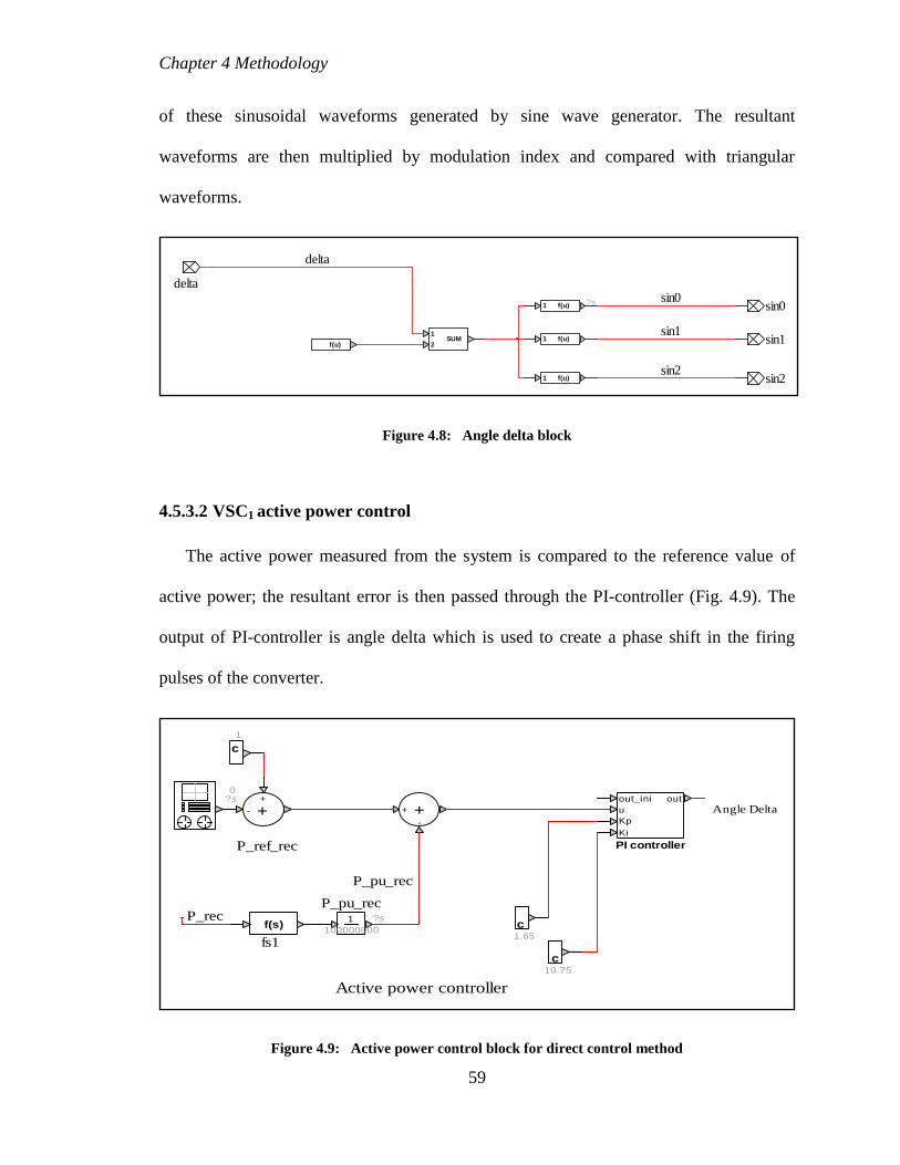
Chapter 4 Methodology
59
of these sinusoidal waveforms generated by sine wave generator. The resultant
waveforms are then multiplied by modulation index and compared with triangular
waveforms.
Figure 4.8: Angle delta block
4.5.3.2 VSC1 active power control
The active power measured from the system is compared to the reference value of
active power; the resultant error is then passed through the PI-controller (Fig. 4.9). The
output of PI-controller is angle delta which is used to create a phase shift in the firing
pulses of the converter.
Figure 4.9: Active power control block for direct control method
f(u)1 ?s
f(u)1
f(u)1
sin0
sin1
sin2
SUM1
2
delta
f(u)
sin0
sin1
sin2
delta
Active power controller
Angle Delta
PI controller
Kp
Ki
out_ini
u
out
c
1
+-
+
P_ref_rec
?s
++
-
c1.65
c10.75
0
1
P_pu_rec?s
100000000f(s)
fs1
P_pu_rec
P_rec
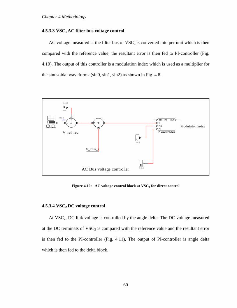
Chapter 4 Methodology
60
4.5.3.3 VSC1 AC filter bus voltage control
AC voltage measured at the filter bus of VSC1 is converted into per unit which is then
compared with the reference value; the resultant error is then fed to PI-controller (Fig.
4.10). The output of this controller is a modulation index which is used as a multiplier for
the sinusoidal waveforms (sin0, sin1, sin2) as shown in Fig. 4.8.
Figure 4.10: AC voltage control block at VSC1 for direct control
4.5.3.4 VSC2 DC voltage control
At VSC2, DC link voltage is controlled by the angle delta. The DC voltage measured
at the DC terminals of VSC2 is compared with the reference value and the resultant error
is then fed to the PI-controller (Fig. 4.11). The output of PI-controller is angle delta
which is then fed to the delta block.
Modulation Index
AC Bus voltage controller
PI controller
Kp
Ki
out_ini
u
out
c
0.83
step
+-
+
V_ref_rec
?s
++
-
c0.4
c10.5
V_bus_r

Chapter 4 Methodology
61
Figure 4.11: DC voltage control block at VSC2 for direct control
4.5.3.5 VSC2 AC filter bus voltage control
The AC voltage measured at the VSC2 filter bus is converted to per unit quantity
which is compared to the reference AC voltage. The resultant error is then fed to the PI-
controller (Fig. 4.12). The output of PI-controller is modulation index which is fed to
PWM block.
Figure 4.12: AC voltage control at VSC2 for direct control
Angle Delta
DC Link Voltage controller
PI controller
Kp
Ki
out_ini
u
out
c
1
0
+-
+
Vdc_ref_inv
?s
++
-
c1.65
c10.75
Vdc_inv
AC Bus voltage controller
Modulation Index
PI controller
Kp
Ki
out_ini
u
out
c
0.89
step
+-
+
V_ref_inv
?s
++
-
c10.5
c0.25
V_bus_i

Chapter 4 Methodology
62
The sinusoidal waveforms coming out of delta block are multiplied by modulation
index to control the amplitude of the sine waveforms which are then compared with the
triangular waveforms. Figure 4.13 shows the direct control system (rectifier controller
and inverter controller) modeled in previous sections using EMTP-RV.
Figure 4.13: Direct control system for VSC-HVDC
RECTIFIER CONTROL BLOCK
Active power controller
Angle Delta
Modulation Index
AC Bus voltage controller
INVERTER CONTROL BLOCK
DC Link Voltage controller
AC Bus voltage controller
Modulation Index
Angle Delta
f1f2f3f4f5f6
a
b
c
mi
p6p5p4p3p2p1
PWM
PULSE
pwmpulse_invPI controller
Kp
Ki
out_ini
u
out
c
1
+-
+?s
P_ref_rec
++
-
c
0.65
c
10.75
PI controller
Kp
Ki
out_ini
u
out
c
0.83
0
+-
+?s
V_ref_rec
++
-
c
0.4
c
10.5
0
1.2
?s
0.7
1
mi_
rec
sin0
sin1
sin2
delta
Delta_Block_1
i1i3i4
i2i5i6
o1o2o3
o4o5o6
DEV8
timedelay
1
100000000
?sP_pu_rec
f(s)
fs1
f1f2f3f4f5f6
a
b
c
mi
p6p5p4p3p2p1
PWM
PULSE
pwmpulse_inv
c
1
0
+-
+?s
Vdc_ref_inv
++
-
c
1.65
c
10.75
PI controller
Kp
Ki
out_ini
u
out
c
0.83
0
+-
+?s
V_ref_inv
++
-
c
10.5
c
0.25
sin0
sin1
sin2
delta
Delta_Block_2
-1
i1
i3i4i2
i5i6
o1
o2o3o4
o5o6
DEV7
timedelay
1.5
?s
0.7
1
lim
1
PI controller
Kp
Ki
out_ini
u
out
rectifier_firing
inverter_firing
V_bus_r
a
Vdc_inv
b
c
V_bus_i
P_rec

Chapter 4 Methodology
63
4.5.4 Vector control system modeling
According to the mathematical model of VSC-HVDC and vector control technique
provided in chapter 3, EMTP-RV blocks are developed and explained in this sub-section.
On the sending end, active and reactive power between filter bus and VSC1 are controlled
whereas on receiving end, DC voltage at VSC2 and reactive power flow between filter
bus and VSC2 are controlled.
4.5.4.1 Modulation Index and Angle delta Block
The modulation index Mi and the angle δ are calculated from the mathematical
representation of the controller output voltage components Vcd and Vcq in synchronously
rotating reference frame. The voltage (Vdc_rec and Vdc_inv) on the DC side of the
converter is measured and converted to per unit value. The angle δ is added to the phase
angle of the control voltages generated locally by the sinusoidal waveform generator.
Equation (4.1) shows the mathematical representation of modulation index Mi and angle
δ,
(4.1)
The aforementioned quantities are realized by using the control block shown in Fig.
4.14 where three sinusoidal modulating waveforms (sina, sinb, sinc) are generated for 3-
phase SPWM.

Chapter 4 Methodology
64
Figure 4.14: Modulation Index and Angle Delta Block
4.5.4.2 Active power control at VSC1
The active power control block consists of outer (Fig. 4.15) and inner current (Fig.
4.16) control loops.
Figure 4.15: Outer current controller loop for active power control block
SINEWAVE GENERATOR
PROD1
2
SUM1
2
SQRT1 DIV
1
2
f(u)1
f(u)1
f(u)1
DIV1
2
Vcq
Vcd
Vdc_rec
mi
sina
sinb
sinc
f(u)
ATAN1
PROD1
2
SUM1
2
Vcd
Vdc_rec
mi
sina
sinb
sinc
Outer current controller whichcontrols the Active power at VSC-1
++
-
error_p_rec
PI controller
Kp
Ki
out_ini
u
out
1.25
-1.25
11
100000000
?s
P_pu_rec
c10
c0.5
f(s)
0
+-
+
P_ref_rec
?s
c0.45
c0.15
P_rec
P_rec
Id_reference
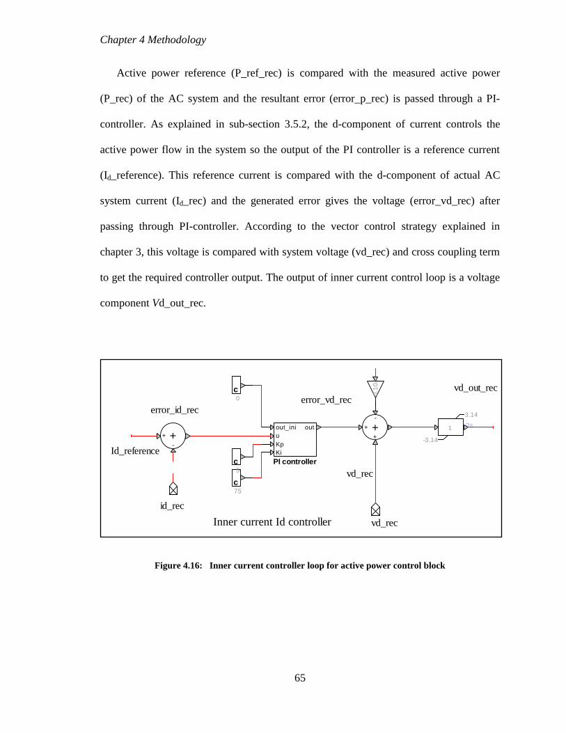
Chapter 4 Methodology
65
Active power reference (P_ref_rec) is compared with the measured active power
(P_rec) of the AC system and the resultant error (error_p_rec) is passed through a PI-
controller. As explained in sub-section 3.5.2, the d-component of current controls the
active power flow in the system so the output of the PI controller is a reference current
(Id_reference). This reference current is compared with the d-component of actual AC
system current (Id_rec) and the generated error gives the voltage (error_vd_rec) after
passing through PI-controller. According to the vector control strategy explained in
chapter 3, this voltage is compared with system voltage (vd_rec) and cross coupling term
to get the required controller output. The output of inner current control loop is a voltage
component Vd_out_rec.
Figure 4.16: Inner current controller loop for active power control block
Inner current Id controller
c75
++
-
error_id_rec
0
.10
4
PI controller
Kp
Ki
out_ini
u
out
c5
3.14
?s
-3.14
1
vd_out_rec
++
+
-
error_vd_recc0
vd_rec
id_rec
Id_reference
vd_rec

Chapter 4 Methodology
66
4.5.4.3 Reactive power control at VSC1
The reactive power controller consists of outer (Fig 4.17) and inner current control
loops (Fig 4.18). As explained in the sub-section 3.5.3, the q-component of the current
controls the reactive power flow in the system. In the outer current control loop, reactive
power reference (Q_ref_rec) is compared with the measured reactive power (Q_rec). The
error is than passed through the PI-controller which gives output in the form of reference
current (Iq_reference) for inner current control loop. This reference current is compared
with the q-component of actual AC system current (Iq_rec) and the generated error gives
the voltage (error_vq_rec) after passing through PI-controller. According to the vector
control strategy explained in chapter 3, this voltage is compared with system voltage
(vq_rec) and cross coupling term to get the required controller output. The output of inner
current control loop is a voltage component Vq_out_rec.
Figure 4.17: Outer current controller loop for reactive power control block
Outer current controller whichcontrols the Reactive power at VSC-1
+-
+?s
Q_ref_rec
PI controller
Kp
Ki
out_ini
u
out
c0.1
c10
++
-
error_q_rec
1
100000000
?s
Q_pu_rec 1
-1
1
c
0
C11c
-0.25
f(s)
0
Q_rec
Iq_reference
Q_rec

Chapter 4 Methodology
67
Figure 4.18: Inner current controller loop for reactive power control block
4.5.4.4 DC voltage control at VSC2
The VSC2 controller supervises the DC link voltage of the VSC-HVDC transmission
system. DC voltage controller consists of outer control loop (Fig 4.19) where the
reference DC voltage (Vdc_ref_inv) is compared with actual DC link voltage (Vdc_inv)
and error is fed to the PI-controller which generates the output in the form of reference
current (Id_reference).
Figure 4.19: Outer current controller for DC voltage control system
Inner current Iq controller
c2
3.14
?s
-3.14
1
Vq_out_rec
PI controller
Kp
Ki
out_ini
u
out ++
-
+
error_vq_rec
++
-
error_iq_rec
0.1
04
c
50
c0
iq_rec
vq_recIq_reference
vq_rec
Outer current controller whichcontrols the DC voltage at VSC-2
++
-
error_p_inv
PI controller
Kp
Ki
out_ini
u
out
1
0.8
1.2
c
1
c
25
c
1
+-
+?s
Vdc_ref_inv
0
c
1
Vdc_invVdc_inv
Id_reference

Chapter 4 Methodology
68
This reference current is compared to the actual d-current component (id_inv) of the
AC system in inner current control loop (Fig 4.20). The output is in the form of voltage
which is then compared to d-component of system voltage (vd_inv) and cross-coupling
term to get the output in the form of voltage (vd_out_inv).
Figure 4.20: Inner current controller for DC voltage control system
4.5.4.5 Reactive power control at VSC2
The reactive power flowing between VSC2 and neighboring AC system is controlled
by reactive power controller at VSC2. The reactive power controller consists of outer
(Fig 4.21) and inner current (Fig 4.22) control loops as well.
Inner current Id controller
+-
-
error_id_inv
0.1
04
PI controller
Kp
Ki
out_ini
u
out
vd_out_inv
1
-3.14
?s
3.14
++
+
-
error_vd_inv
c C2
35
c
1
c
3
vd_inv
id_inv
Id_reference
vd_inv
iq_inv
id_inv

Chapter 4 Methodology
69
Figure 4.21: Inner current controller loop for reactive power control block
Figure 4.22: Outer current controller loop for reactive power control block
In the outer current control loop, reactive power reference (Q_ref_inv) is compared
with the measured system reactive power (Q_inv). The error is than passed through the
PI-controller which gives output in the form of reference current (Iq_reference). This q-
Outer current controller whichcontrols the Reactive power at VSC-2
+-
+
Q_ref_inv
?s
c
20
++
-
error_q_inv
1
Q_pu_inv?s
1000000001
-1
1
c
0
c
-0.25
f(s)
0
PI controller
Kp
Ki
out_ini
u
out
c
0.25
Q_inv
Iq_reference
Q_inv
Inner current Id controller
vq_out_inv
1
-3.14
?s
3.14
PI controller
Kp
Ki
out_ini
u
out ++
-
+
error_vq_inv
++
-
error_iq_inv
0.1
04
c25
c
0.5
c
2
vq_inv
iq_inv
Iq_reference
iq_inv
vq_inv
id_inv

Chapter 4 Methodology
70
component of the current controls the reactive power flow in the system so it is used as a
reference current for the inner current controller and compared with q-component of
measure AC current (iq_inv). The error (error_iq_inv) gives voltage after passing through
PI-controller. This voltage is then compared to the q-component of voltage (vq_inv) and
cross coupling term to get the controller output voltage (vq_out_inv).
4.5.5 PI-Controller Gains
The PI-controller gains for all four controllers are provided in Table 4-3. From the
table it is evident that the gains of the inner current controllers are higher than outer
current controller to ensure the stability of the system. Proportional gain KP helps to reach
the reference value quickly whereas the integral gain KI ensures zero steady state error.
Table 4-3 VSC-HVDC PI-controller gains
Controllers
Outer current controller
gains
Inner current controller
gains
KP KI KP KI
Active power (VSC1) 0.15 10 5 75
Reactive power (VSC1) 0.1 10 2 50
DC voltage (VSC2) 1 25 3 35
Reactive power (VSC2) 0.25 20 2 25
Figure 5.23 shows the power system modeling of proposed VSC-HVDC simulation
model in EMTP-RV. Figure 5.24 shows the rectifier control block and Fig 5.25 shows the
inverter control block of proposed VSC-HVDC system model with vector control
strategy.

Chapter 4 Methodology
71
Figure 4.23: VSC-HVDC model created using EMTP-RV software package
RECTIFIER CONTROL BLOCK INVERTER CONTROL BLOCK
DC TRANSMISSION SYSTEMVOLTAGE SOURCE CONVERTER (VSC) -1 VOLTAGE SOURCE CONVERTER (VSC) -2 RECEIVING END AC TRANSMISSION SYSTEMSENDING END AC TRANSMISSION SYSTEM
+
AC1
230kVRMSLL /_0
FIL
TE
RS
RLCFILTERS
+
230kVRMSLL /_0
AC2P ic
60Hz
P_rec+
467mH
?v
L1
Qic
60Hz
Q_rec
i(t)?s
I_inv
DC2 Pc
Pb
PaDC1
fir
ing
33
VSC2
i(t)
?s
I_rec
P ic
P_inv
60Hz
FIL
TE
RS
RLCFILTERS
1 2
230/49
YY2
+
C37
0.075uF
+
L2?v
467mH
+
C1
0.075uF
Q ic
Q_inv
60HzDC2Pc
Pb
Pa DC1
fir
ing
33
VSC1
v (t)
V_source_rec
v (t)?s
V_conv_recv (t)
V_conv_inv
?s v (t)
V_source_inv
1 2
49/230
YY1
rectifier_firing
P_rec
Q_rec
Vdc_rec
vd_rec
iq_rec
vq_rec
id_rec
1
rectifier_controllerI_c_inv
I_b_inv
I_a_inv
V_bus_invvd_inv
iq_inv
vq_inv
id_inv
DEV2
conversion
inverter_firing
Q_inv
Vdc_inv
vd_inv
iq_inv
vq_inv
id_inv
2
Inverter_controller
BA C
Fault_1
p1
p2
p3
p4
Vd
c_
re
c
Vd
c_
inv
I_c_rec
I_b_rec
I_a_rec
vd_recV_bus_rec
iq_rec
vq_rec
id_rec
DEV11
BA C
DEV1
Fault_2
I_a_rec
I_a_rec
I_c_rec
I_c_rec
I_b_rec
I_b_rec
P_inv
V_source_rec
I_b_inv
I_b_inv
I_a_inv
I_a_inv
I_c_inv
I_c_inv
c
b
a
V_conv_inv
c
b
aV_conv_rec
V_source_inv
V_bus_rec
cba
V_bus_rec
V_bus_invabc
V_bus_inv
P_rec
P_rec
Q_rec
Q_rec Q_inv
Q_inv
Vdc_rec
Vdc_rec
Vdc_inv
Vdc_inv
rectifier_firing
inverter_firing

Chapter 4 Methodology
72
Figure 4.24: Rectifier Control Block of Proposed VSC-HVDC model
Inner current Id controller
Outer current controller whichcontrols the Reactive power at VSC-1
Inner current Iq controller
Outer current controller whichcontrols the Active power at VSC-1
f1f2f3f4f5f6
a
b
c
mi
p6p5p4p3p2p1
PWM
PULSE
DEV1
pwmpulse_rec
c75
++
-
error_id_rec
0
.10
4
PI controller
Kp
Ki
out_ini
u
out
c5
c2
3.14
?s
-3.14
1
Vq_out_rec
PI controller
Kp
Ki
out_ini
u
out ++
-
+
error_vq_rec
++
-
error_iq_rec
0.1
04
c
50
+-
+?s
Q_ref_rec
3.14
?s
-3.14
1
vd_out_rec
++
-
error_p_rec
PI controller
Kp
Ki
out_ini
u
out
PI controller
Kp
Ki
out_ini
u
out
c0.1
c10
++
-
error_q_rec
++
+
-
error_vd_rec
1
100000000
?s
Q_pu_rec
1.25
-1.25
1
1
-1
1
1
100000000
?s
P_pu_rec
c
0
C11
c10
c0.5
c-0.25
f(s)
f(s)
0
0
+-
+
P_ref_rec
?s
c0.45
c0.15
c0
c0
Vcq
Vcd
Vdc_recmi
sin0
sin1
sin2
DEV2
Mi_delta_reci1
i3i4i2
i5i6
o1
o2o3o4
o5o6
timedelay
DEV12
P_rec
Q_rec
Vdc_rec
vd_rec
iq_rec
vq_rec
id_rec
rectifier_firing
Iq_reference
P_rec
Q_rec
Id_reference
Vdc_rec
vd_rec
iq_rec
vq_rec
id_rec
rectifier_firing

Chapter 4 Methodology
73
Figure 4.25: Inverter control block for proposed VSC-HVDC model
Outer current controller whichcontrols the DC voltage at VSC-2
Outer current controller whichcontrols the Reactive power at VSC-2
Inner current Id controller
Inner current Id controller
f1f2f3f4f5f6
a
b
c
mi
p6p5p4p3p2p1
PWM
PULSE
pwmpulse_inv
DEV4
+-
-
error_id_inv
0.1
04
PI controller
Kp
Ki
out_ini
u
out
vq_out_inv
1
-3.14
?s
3.14
PI controller
Kp
Ki
out_ini
u
out ++
-
+
error_vq_inv
++
-
error_iq_inv
0
.10
4
c25
vd_out_inv
1
-3.14
?s
3.14
++
-
error_p_inv
PI controller
Kp
Ki
out_ini
u
out
++
+
-
error_vd_inv
1
0.8
1.2
c C2
35
c
1
c
25
c
1
+-
+?s
Vdc_ref_inv
0
c
1
c
0.5
+-
+
Q_ref_inv
?s
c
20
++
-
error_q_inv
1
Q_pu_inv?s
1000000001
-1
1
c
0
c
-0.25
f(s)
0
PI controller
Kp
Ki
out_ini
u
out
c
2
c
3
c
1
c
0.25
Vcq_inv
Vcd_inv
Vdc_invmi
sin0
sin1
sin2
DEV6
Mi_delta_inv
i1i3
i4i2i5
i6
o1o2
o3o4o5
o6
timedelay
DEV14
Q_inv
Vdc_inv
vd_inv
vq_inv
inverter_firing
iq_inv
id_inv
Iq_reference
Id_reference
Q_inv
Vdc_inv
Vdc_inv vd_inv
iq_inv
iq_inv
vq_inv
id_inv
id_inv
inverter_firing

Chapter 4 Methodology
74
4.6 Summary
In this chapter, all the components of the VSC-HVDC system have been explained
regarding required rating and the modeling technique adopted. Modeling of AC and DC
Power system, transformers, AC filters, IGBT-diode unit and VSC is done here. Two
control methods; direct control and vector control method are explained and detailed
modeling of control blocks is provided. For vector control technique, inner and outer
current control loops for all four controllers are modeled and proportional and integral
gains of PI-controllers for all controllers are also provided in this chapter. The VSC-
HVDC system model developed in EMTP-RV software package is provided here.

75
Chapter 5
Simulation Results and Analysis
5.1 Introduction
This chapter focuses on the VSC-HVDC performance assessment during steady state
and dynamic state; step changes in active power, reactive power/AC voltage and DC
voltage, and active and reactive power flow reversals using the EMTP-RV simulation
model. The simulation results with direct control and vector control techniques are
provided and comparison is done regarding independent control of quantities (Active
power, reactive power/AC voltage). Table 5-1 presents the system parameters and ratings
of the VSC-HVDC system. Since the control systems of the VSC-HVDC use high
frequency (1440 Hz) sinusoidal PWM method, the VSC-HVDC model is simulated with
a time step of 5 µs. By using a small time step, it is possible to observe the system
response comprehensively during system start-up, step changes and fault applications.
However, this does slow down the simulation process and generates a huge amount of
data for signal processing purposes.
Table 5-1: Parameters of VSC-HVDC Simulation Model
Parameters Rating
System Power Level 100 MVA
Frequency 60 Hz
Converter Transformer Primary voltage 230 kV
Converter Transformer Secondary voltage 49 kV
DC Voltage ± 40 kV
Switching Frequency of PWM 1440 Hz
Source Impedance (Inductance) 176.1 Ω (467 mH)
DC Cable Length 75 km
AC Filter Rating 70 MVAR

Chapter 5 Simulation Results and Analysis
76
5.2 Steady state operation-Direct control method
The steady-state operational performance of the VSC-HVDC system with direct
control scheme is investigated by considering various operating conditions and reference
values of the system quantities.
5.2.1 Case study-1
Case study-1 presents the operation of VSC-HVDC system in an active power flow
state with constant AC and DC voltages. The active power of 1 pu flows from VSC1 to
VSC2 (Fig. 5.1a) whereas the filter bus AC voltages at both ends (Fig. 5.1b & 5.1c) of the
system and the DC voltage are maintained constant at 1 pu (Fig. 5.1d).
Figure 5.1: Steady-state operation of VSC-HVDC with direct control method (a) 1 pu active power
flow from VSC1 to VSC2 (b) 1 pu AC bus voltage at VSC1 filter bus (c) 1 pu AC bus voltage at VSC2
filter bus (d) 1 pu DC link voltage

Chapter 5 Simulation Results and Analysis
77
It is evident that system attains all the reference values within the time of 1 s. There
are some transients seen in active power, AC voltages and DC voltage during the system
start-up which decays within 0.4 s.
5.2.2 Case-study-2
Figure 5.2a shows the scenario of 1 pu active power flow from VSC2 to VSC1 with
filter bus AC voltages at either end (Fig. 5.2b & 5.2c) and DC voltage (Fig. 5.2d)
maintained at 1 pu. Again, it is seen that the system operates with same stability as in the
previous case which proves the ability of VSC-HVDC to operate in bi-directional power
flow mode. Active power reaches the reference value within 1 s.
Figure 5.2: Steady-state operation of VSC-HVDC with direct control method (a) 1 pu active power
flow from VSC2 to VSC1 (b) 1 pu AC bus voltage at VSC1 filter bus (c) 1 pu AC bus voltage at VSC2
filter bus (d) 1 pu DC link voltage

Chapter 5 Simulation Results and Analysis
78
The DC voltage has nearly 50 % overshoot before reaching the reference value and the
filter bus AC voltages at VSC1 and VSC2 track the reference value within 1s.
5.3 Step changes-Direct control method
In this case, step changes in active power, DC voltage and AC voltages are
implemented in all four VSC-HVDC controllers. Two of these disturbances are applied at
the converter VSC1 which controls (a) the active power between AC system and DC
transmission system and (b) AC voltage at VSC1 filter bus and the other two disturbances
are applied at the VSC2 which controls (c) the DC voltage and (d) AC voltage at VSC2
filter bus. By applying steps in all four controllers at different times, VSC-HVDC
system’s capability of recovery after disturbances is studied.
As shown in Fig. 5.3a, initially active power of 0.5 pu flows from VSC2 to VSC1. A
negative step of 25% is applied at 1.5 s for duration of 0.5 s in active power controller at
VSC1. First, the active power follows the reference value with little overshoot and
settling time of 0.15 s. Second, it can be seen that the change in active power affects the
AC voltages on both AC systems by creating some transients when the step is applied
and a clear effect in the DC voltage is also observable.
Next, in Fig. 5.3b, initially AC voltage at VSC1 filter bus is at 1 pu. A negative step of
10% is applied at 2.5 s for duration of 0.5 s in the AC voltage at VSC1 filter bus. It can
be seen that the change in AC voltage affects neither the active power on same side nor
the AC voltage on other side of the VSC-HVDC system and DC link voltage.

Chapter 5 Simulation Results and Analysis
79
In Fig. 5.3c, initially AC voltage at VSC2 filter bus is at 1 pu. At 3.5 s negative step of
10% is applied for 0.5 s in the AC voltage at VSC2 filter bus. The step in AC voltage at
VSC2 affects neither the active power and AC voltage at VSC1 nor the DC voltage at
VSC2.
In Fig.5.3d, initially the DC voltage is maintained constant at 1 pu which is followed
by a negative step of 10% applied at 4.5 s for 0.5 s in DC voltage controller at VSC2.
First, the transition is observed to be rapid, well controlled with overshoot of about 10%
and settling time of 0.5 s. Second, it can be seen that the change in DC voltage affects
the AC voltages on both sides of the VSC-HVDC system. The active power at VSC1 gets
some disturbance due to step in DC voltage controller at VSC2.
Figure 5.3: Dynamic-state operation of VSC-HVDC with direct control method (a) 0.5 pu active
power flow from VSC2 to VSC1 (b) 1 pu AC bus voltage at VSC1 filter bus (c) 1 pu AC bus voltage at
VSC2 filter bus (d) 1 pu DC link voltage

Chapter 5 Simulation Results and Analysis
80
Sequence of events:
Time Action
1.5-2 sec 25 % negative step in active power which flows from VSC2 to VSC1
2.5-3 sec 10 % negative step in reactive power flowing from AC system to VSC1
3.5-4 sec 10 % negative step in reactive power flowing from VSC1 to AC system
4.5-5 sec 10 % negative step in DC link voltage
5.4 Active power flow reversal-Direct control method
In Fig. 5.4a, the initial reference value of the power flow is at +0.5 pu in the direction
from VSC2 (rectifier mode) to VSC1 (inverter mode). At 1.5 s, the reference value is
reversed from +0.5 pu to -0.5 pu. It can be seen that the active power follows the
reference rapidly without any oscillation and reaches the new reference of -0.5 pu within
0.4 s. During this power reversal, some transients are observed in AC voltages at both
ends as shown in Fig. 5.4b and Fig. 5.4c and DC voltage has large overshoot of nearly 40
% which stabilizes within 0.5 s.
In Fig. 5.4b, initially the AC voltage at VSC1 filter bus is at 1 pu. At 2.5 s, the
reference value is changed to 0.9 pu. The AC voltage follows the reference value quickly
and stabilizes within 0.25 s without any kind of oscillations. It is observed that this
change does not create any effect on active power at VSC1 or AC voltage and DC voltage
at VSC2.
In Fig. 5.4c, initially the VSC2 filter bus AC voltage reference is at 1 pu. At 3.5 s, the
reference value is changed to 1.1 pu and as seen, the VSC2 filter bus AC voltage follows
the reference value within 0.2 s without any transients.

Chapter 5 Simulation Results and Analysis
81
Next, Fig. 5.4d shows the variation of DC voltage throughout the process of changes
applied to other controllers in the system as shown in Fig 5.4a, 5.4b and 5.4c. During
active power flow direction change, there is a overshoot of 35 % in the value of DC
voltage. The change in AC voltage at both ends does not have any effect on DC voltage.
Figure 5.4: Steady-state operation of VSC-HVDC with direct control method (a) Initially 0.5 pu
active power flow from VSC2 to VSC1 (b) Initially 1 pu AC bus voltage at VSC1 filter bus (c) Initially
1 pu AC bus voltage at VSC2 filter bus (d) DC link voltage is maintained constant at 1 pu
Sequence of events:
Time Action
1.5 sec Active power flow direction changes from +0.5 pu to -0.5 pu
2.5 sec Filter bus voltage (VSC1) value changes from 1 pu to 0.9 pu
3 sec Filter bus voltage (VSC2) value changes from 1 pu to 1.1 pu
DC voltage is maintained constant at 1 pu

Chapter 5 Simulation Results and Analysis
82
5.5 Steady state operation -vector control method
The steady-state operational performance assessment of the VSC-HVDC system
comprises of vector control technique is investigated by considering various operating
conditions and reference values of system quantities. The system modeled here is bi-
directional so active power and reactive powers can flow in both directions according to
the system requirements and operating conditions.
5.5.1 Case study-1
Case study-1 presents the operation of VSC-HVDC system in an active power flow
state only. The active power of 0.45 pu flows from VSC2 to VSC1 (Fig 5.5a) whereas the
reactive power flow at both ends (Fig 5.5b & 5.5d) of the system is zero and the DC
voltage is maintained at 1 pu (Fig 5.5c). It is evident that system attains all the reference
values within the time of 0.4 s. There are some transients seen in active power, reactive
powers and DC voltage during the system start-up with decays within 0.3 s.
Active power and DC voltage get the overshoot of nearly 25 % and 50 % respectively
which may be reduced by further optimizing the gains of PI-controllers. The reactive
powers at both ends achieve the reference values within 0.4 s after initial negative and
positive transients along the reference value.

Chapter 5 Simulation Results and Analysis
83
Figure 5.5: Steady-state operation of VSC-HVDC (a) 0.45 pu active power flow from VSC2 to VSC1
(b) Reactive power of 0 pu at VSC1 (c) DC voltage of 1 pu in DC link (d) Reactive power of 0 pu at
VSC2
5.5.2 Case study-2
Figure 5.6a shows the situation of 0.45 pu active power flow from VSC1 to VSC2 with
zero reactive power flow at either end (Fig 5.6b & 5.6d) and 1 pu DC voltage (Fig 5.6c).
Again, it is seen that the system operates with same stability as in the previous case
which proves the ability of VSC-HVDC to operate in bi-directional power flow mode.
Active power reaches the reference value within 0.4 s without any oscillations The DC
voltage has nearly 40 % overshoot before reaching the reference value and the reactive
powers at VSC1 and VSC2 follow the reference value within 0.2 s.

Chapter 5 Simulation Results and Analysis
84
Figure 5.6: Steady-state operation of VSC-HVDC (a) 0.45 pu active power flow from VSC1 to VSC2
(b) Reactive power of 0 pu at VSC1 (c) DC voltage of 1 pu in DC link (d) Reactive power of 0 pu at
VSC2
5.5.3 Case study-3
This case presents the full load operation of the system with active power flow of 1
pu from VSC1 to VSC2 (Fig 5.7a) along the HVDC transmission system. At VSC1, the
reactive power (Fig 5.7b) of 0.65 pu flows from converter to AC system which shows the
capacitive mode of operation of converter. At VSC2, the reactive power (Fig 5.7d) of 0.45
pu flows from AC system to converter which shows the inductive mode. The DC voltage
(Fig 5.7c) remains constant at 1 pu followed by an overshoot of 45 % during system start
up. The dissimilar amount of reactive power flows in different direction at both ends of
VSC-HVDC. In this case study, the independent control of reactive power is explained

Chapter 5 Simulation Results and Analysis
85
which is of importance when VSC-HVDC supplying the passive networks or connecting
weak AC networks.
Figure 5.7: Full load active power flow (a) 1 pu active power flow from VSC1 to VSC2 (b) 0.65 pu
reactive power flow from VSC1 to AC system (c) DC voltage of 1 pu in DC link (d) 0.45 pu reactive
power flow from AC system to VSC2
5.5.4 Case study-4
This case presents the full load operation of the system with active power flow of 1
pu from VSC2 to VSC1 (Fig 5.8a) along the HVDC transmission system. At VSC1, the
reactive power (Fig 5.8b) of 0.25 pu flows from converter to AC system. At VSC2, the
reactive power (Fig 5.8d) of 0.5 pu flows from converter to AC system. The DC voltage
(Fig 5.8c) attains the reference value of 1 pu with in 0.5 s. This case study explains the

Chapter 5 Simulation Results and Analysis
86
converter operation in the inductive mode, where both the converters VSC1 and VSC2
absorb the reactive power from the system.
Figure 5.8: Full load active power flow (a) 1 pu active power flow from VSC2 to VSC1 (b) 0.25 pu
reactive power flow from VSC1 to AC system (c) DC voltage of 1 pu in DC link (d) 0.5 pu reactive
power flow from VSC2 to AC system
5.6 Step changes -vector control method
In this case, step changes in active power, DC voltage and reactive power are
implemented in all four VSC-HVDC controllers. Two of these disturbances are applied at
the converter VSC1 which controls (a) the active power between AC system and DC
transmission system and (b) reactive power at VSC1. Two of the disturbances are applied
at the VSC2 which controls (c) the DC voltage and (d) reactive power at VSC2. In this
Chapter 5 Simulation Results and Analysis
87
one test, in reality, four separate disturbances are implemented to understand the system’s
ability to recover during disturbances.
As shown in Fig. 5.9a, initially active power of 0.5 pu flows from VSC2 to VSC1. A
negative step of 25% is applied at 1 s for duration of 0.6 s in active power controller at
VSC1. First, the transition is observed to be well controlled with little overshoot and
settling time of 0.35 s. Second, it can be seen that the change in active power does not
affect the reactive powers on either side of the AC systems though there are some
transients observed when the step is applied. A noticeable effect in the DC voltage is
observable and the size of the DC capacitor employed will have an impact on this.
Next, in Fig. 5.9b, initially reactive power of 0.5 pu flows from AC system to VSC1.
A negative step of 25% is applied at 2.35 s for duration of 0.6 s in the reactive power
controller at VSC1. First, the transition is observed to be well controlled with little
overshoot and settling time of 0.35 s. Second, it can be seen that the change in reactive
power affects neither the active power on same side nor the reactive power on other side
of the AC system. This clearly demonstrates the independence of the P and Q controllers
at the VSC1 end.
In Fig.5.9c, initially the DC voltage is maintained constant at 1 pu which is followed
by a positive step of 10% applied at 3.7 s for 0.6 s in DC voltage controller at VSC2.
First, the transition is observed to be rapid, well controlled with overshoot of about 5%
and settling time of 0.15 s. Second, it can be seen that the change in DC voltage does
affect the reactive powers on either side of the AC systems. Naturally, the size of DC
capacitor will be a significant element in controlling this effect.

Chapter 5 Simulation Results and Analysis
88
Next, in Fig. 5.9d, initially 0.5 pu reactive power flows from VSC2 to VSC1, at 5.05 s
positive step of 25% is applied for 0.6 s in reactive power at VSC2. First, the transition is
observed to be well controlled with little overshoot and 0.15 s settling time. Second, it
can be seen that, there are some transients observed when the step is applied. The steps in
reactive power at both ends do not affect the active power and DC voltage.
Figure 5.9: Step changes in the active power, reactive power and DC voltage (a) 0.5 pu active power
flow from VSC2 to VSC1 (b) 0.5 pu reactive power flow from AC system to VSC1 (c) DC voltage of 1
pu in DC link (d) 0.5 pu reactive power flow from VSC2 to AC system
Sequence of events:
Time Action
1-1.6 sec 25 % negative step in active power which flows from VSC2 to VSC1
2.35-2.95 sec 25 % negative step in reactive power flowing from AC system to VSC1
3.7-4.3 sec 10 % positive step in DC link voltage
5.05-5.65 sec 25 % positive step in reactive power flowing from VSC1 to AC system

Chapter 5 Simulation Results and Analysis
89
5.7 Active and reactive power reversal -vector control method
In this case study, the reference values of P and Q controllers are changed so as to
reverse the active and reactive power whilst keeping DC voltage constant. The behaviors
of all four controllers are observable in this case.
In Fig. 5.10a, the initial reference value of the power flow is at +0.5 pu in the
direction from VSC2 (rectifier mode) to VSC1 (inverter mode). At 1 s, the reference value
is reversed from +0.5 pu to -0.5 pu. It can be seen that the active power follows the
reference rapidly without any oscillation and reaches the new reference of -0.5 pu within
0.4 s. During this power reversal, some transients are observed in reactive power at both
ends as shown in Fig. 5.10b and Fig. 5.10c and DC voltage has large overshoot of nearly
40 % which stabilizes within 0.3 second. Due to system parameters it is not feasible to
reverse the full power instantaneously.
Fig. 5.10b shows a large change in reactive power at VSC1. Initially the reactive
power reference is at +0.15 pu which flows from AC system to VSC1. At 2 s, the
reference value is reversed to -0.15 pu. The direction change in the flow of reactive
power is stabilized within 0.35 s without any kind of oscillations. It is observed that this
disturbance does not create any kind of effect on active power or reactive power at VSC2.
There is virtually little effect on the DC voltage due to this reversal of reactive power.
In Fig. 5.10c, initially the reactive power reference at VSC2 is at -0.5 pu which flows
from converter to AC system. At 3 s, the reference value is changed to +0.5 pu and as
seen in the Fig. 5.10c, the reactive power at VSC2 follows the reference value within 0.2 s
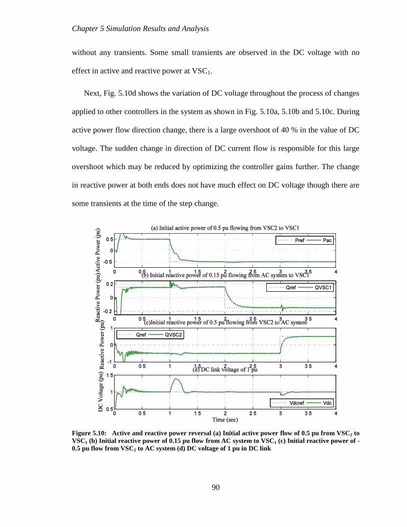
Chapter 5 Simulation Results and Analysis
90
without any transients. Some small transients are observed in the DC voltage with no
effect in active and reactive power at VSC1.
Next, Fig. 5.10d shows the variation of DC voltage throughout the process of changes
applied to other controllers in the system as shown in Fig. 5.10a, 5.10b and 5.10c. During
active power flow direction change, there is a large overshoot of 40 % in the value of DC
voltage. The sudden change in direction of DC current flow is responsible for this large
overshoot which may be reduced by optimizing the controller gains further. The change
in reactive power at both ends does not have much effect on DC voltage though there are
some transients at the time of the step change.
Figure 5.10: Active and reactive power reversal (a) Initial active power flow of 0.5 pu from VSC2 to
VSC1 (b) Initial reactive power of 0.15 pu flow from AC system to VSC1 (c) Initial reactive power of -
0.5 pu flow from VSC2 to AC system (d) DC voltage of 1 pu in DC link

Chapter 5 Simulation Results and Analysis
91
Sequence of events:
Time Action
1 sec Active power flow direction changes from +0.5 pu to -0.5 pu
2 sec Reactive power flow (VSC1) direction changes from +0.15 pu to -0.15pu
3 sec Reactive power flow (VSC2) direction changes from -0.5 pu to +0.5 pu
DC voltage is maintained constant at 1 pu
5.8 Comparison between direct and vector control technique
The simulation results for step changes of the VSC-HVDC system with direct control
technique and vector control technique are shown in Fig. 5.3 and Fig. 5.9 respectively. As
shown, the step changes are applied in the active power, reactive power /AC voltages and
DC voltage.
In Fig. 5.3, it is evident that the step change in active power strongly creates the
transients in AC voltages at both ends and DC link voltage. Same way, the step in DC
voltage has created large transients in active power and AC voltages at both ends of the
VSC-HVDC system.
In Fig. 5.9, it is seen that the change in active power affects neither the reactive
powers at either end nor the DC voltage at VSC2. The step in DC voltage has created a
small transient in reactive power flow at VSC2 whereas there is no effect on the active
power and reactive power at VSC1.
In case of direct control method; due to coupling between electrical quantities, change
in one quantity strongly affects the other quantity. Whereas in case of vector control

Chapter 5 Simulation Results and Analysis
92
technique, the coupling is removed so change in one parameter does not create any effect
on other parameter in the system. This is a major advantage of vector control method
compared to direct control method. As described earlier, in direct control method,
modulation index and angle delta are controlled directly whereas in vector control
technique modulation index and angle delta is derived using de-coupled feed forward
control loops. By using vector control, the coupling between these electrical quantities is
removed so change in one quantity does not affect the other quantity.
5.9 Effect of DC capacitance on VSC-HVDC performance
The DC side capacitors play a vital role on the system performance. The role of DC
capacitors is described in section 2.2.5. The charging and discharging of DC capacitors
according to the current flow and hence the power flow takes place in the DC
transmission system. The step changes in active power, reactive power and DC voltages
are applied for different values of DC capacitors. Figure 5.11 shows the results with the
two 200µF DC capacitors connected in series across the DC terminals of VSC at both
ends. It is seen that even though the system operates in stably, the transients in active
power, reactive powers at both ends and DC voltage are very high which may lead the
system to instability.

Chapter 5 Simulation Results and Analysis
93
Figure 5.11: Step changes with the DC capacitance of 100µF at each terminal
As the value of DC capacitor increases, the transients in all four quantities are
reduced. Fig. 5.12, 5.13 and 5.14 show the simulation results with DC capacitor size of
200µF, 300µF and 400µF respectively. The transients in 400µF DC capacitance are least
compared to any other lower size capacitor.
Figure 5.12: Step changes with the DC capacitance of 200µF at each terminal

Chapter 5 Simulation Results and Analysis
94
Figure 5.13: Step changes with the DC capacitance of 300µF at each terminal
Figure 5.14: Step changes with the DC capacitance of 400µF at each terminal
Chapter 5 Simulation Results and Analysis
95
5.10 Summary
In this chapter, the VSC-HVDC system modeled in chapter 4 is simulated using
EMTP-RV software package. Two different control techniques; direct and vector control
are considered for simulation studies. The simulation studies regarding the various
operating conditions, reference value changes and reversal of active and reactive power
are carried out and analyzed. The comparison of two control techniques regarding the
operational performance during step changes is done here. The size of DC capacitor
affects the system performance, and a comparative study with four capacitor values was
performed.

96
Chapter 6
Fault Analysis
6.1 Introduction
The VSC-HVDC model developed in EMTP-RV in chapter 4 is studied regarding
symmetrical and asymmetrical faults on sending and receiving end AC networks and
fault on DC transmission system. Vector control strategy is implemented during this
analysis. The different electrical quantities like voltage, current, active power and
reactive powers at both AC sides and voltage and current in DC link are studied to
understand the system behavior under the fault conditions. From this analysis, the ability
of VSC-HVDC system to remain in stability and to decouple two connected AC systems
is determined.
6.2 Fault analysis at VSC1
Various symmetrical and asymmetrical faults at the VSC1 converter transformer high
voltage (HV) filter bus were created. The starting conditions are implemented such as
active power of 0.45 pu flows from VSC2 to VSC1, the reactive power flow at either end
is zero and the DC voltage is at 1 pu.

Chapter 6 Fault Analysis
97
6.2.1 Single line to ground (SLG) fault at VSC1
A SLG fault in phase A is created at 0.75 s for 6 cycles (100 ms) at HV side of VSC1
converter transformer. Figures 6.1a, b, c and d show the phase A voltage and current
waveforms at VSC1 and VSC2 AC filter bus respectively. During the fault, phase A
voltage at VSC1 becomes nearly zero and high amplitude fault current flows with
oscillations.
Figure 6.1: SLG fault at VSC1 converter transformer

Chapter 6 Fault Analysis
98
The phase A voltage at VSC2 is stable during this fault which shows no effect of the
fault on the unfaulted side of the HVDC transmission system. The phase A current on
VSC2 is stable though it gets some disturbance which stabilizes within 4 cycles. The
distortion can be seen in DC link voltage and current (Fig. 6.1e & 6.1f) which reflects
slow response to the fault and follows the reference value within 0.4 s. When the fault is
removed, the voltage at VSC1 stabilizes within 5 cycles. The fault impedance of 1mH and
5 Ω is utilized during this fault condition.
6.2.2 Asymmetrical double line to ground (DLG) fault on AC filter bus
at VSC1
A DLG fault in phase A and B is created at 0.75 s for 6 cycles at the VSC1 converter
transformer HV side. Figures 6.2a, b, c and d show the phase A and B voltage and current
waveforms at AC filter bus of VSC1 and VSC2 respectively. During the fault, it is seen
that the phase A and B voltages at VSC1 reach nearly 40 % of their rated value and high
fault currents flow from phase A and B to ground. The voltages at VSC2 are stable
during this fault which shows the ability of VSC-HVDC to decouple systems during fault
conditions on neighboring AC systems. The currents at VSC2 show some distortion
which decay within 5 cycles. The DC link voltage oscillates between 1.1 pu and 0.8 pu
before returning to the reference value of 1 pu. When the fault is removed, the voltages at
VSC1 stabilize within 5 cycles. A fault impedance of 1mH and 65 Ω was utilized during
this fault condition.

Chapter 6 Fault Analysis
99
Figure 6.2: DLG fault at VSC1 converter transformer
6.2.3 Symmetrical three lines to ground (TLG) fault on AC filter bus at
VSC1
A TLG fault was created at 0.75 s for 6 cycles at the VSC1 converter transformer HV
side. The voltage and current waveforms of all the phases at AC filter bus of VSC1 and
VSC2 are shown in Fig. 6.3a, b, c and d respectively. It is seen that during the fault, the
voltages at the VSC1 becomes nearly 60 % of rated value and distorted fault currents flow
to ground. The VSC-HVDC operates as a shock absorber during the faults so the
voltages at VSC2 are stable during this fault. The currents at VSC2 get minor disturbance
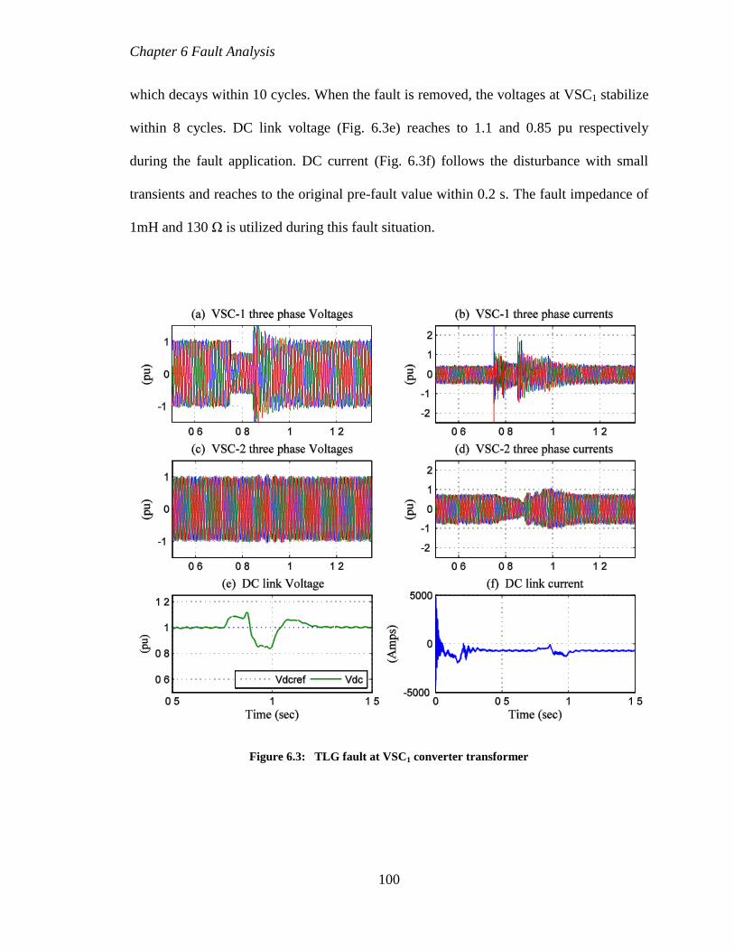
Chapter 6 Fault Analysis
100
which decays within 10 cycles. When the fault is removed, the voltages at VSC1 stabilize
within 8 cycles. DC link voltage (Fig. 6.3e) reaches to 1.1 and 0.85 pu respectively
during the fault application. DC current (Fig. 6.3f) follows the disturbance with small
transients and reaches to the original pre-fault value within 0.2 s. The fault impedance of
1mH and 130 Ω is utilized during this fault situation.
Figure 6.3: TLG fault at VSC1 converter transformer

Chapter 6 Fault Analysis
101
6.3 Fault analysis at VSC2
Different symmetrical and unsymmetrical faults are produced at VSC2 converter
transformer HV bus. The active power of 0.45 pu flows from VSC2 to VSC1, reactive
power flow is zero at either end and DC link voltage is maintained at 1 pu during all the
fault conditions considered here.
6.3.1 Single line to ground fault at VSC2
Single line to ground fault in phase A is created at 0.75 s for 6 cycles at HV side of
the VSC2 converter transformer. Figures 6.4a and 6.4c show the voltage waveforms at
AC filter bus of VSC2 and VSC1 respectively. It is seen that during the fault, the voltage
at the VSC2 becomes nearly 15 % of rated value whereas the AC bus voltage at VSC1 is
stable during this fault which shows no effect of the fault on the other side of the HVDC
transmission system. After the fault is removed, the voltage at VSC2 becomes stable
within 5 cycles.
The distortion can be seen in DC link voltage and current (Fig. 6.2e & 6.2f) which
reflects slow response to the fault and follows the reference value within 0.4 s. A fault
impedance of 1mH and 60 Ω is utilized during this fault situation.

Chapter 6 Fault Analysis
102
Figure 6.4: SLG fault at VSC2 converter transformer
6.3.2 Asymmetrical double line to ground fault on AC filter bus at VSC2
Asymmetrical double line to ground fault in phase A and B is created at 0.75 s for 6
cycles at HV side of the VSC2 converter transformer. Figures 6.5a and 6.5c show the
voltage waveforms of phase A and B at AC filter bus of VSC2 and VSC1 respectively. It
is seen that during the fault, the voltages of phase A and B at the VSC2 becomes nearly 70
% with distortion whereas the voltage VSC1 is stable during this fault. When the fault is
removed, the voltage at VSC2 becomes stable within 5 cycles. The disturbance is seen in

Chapter 6 Fault Analysis
103
DC current during fault application (Fig 6.5f). The fault impedance of 1mH and 135 Ω is
utilized during this fault situation.
Figure 6.5: DLG fault at VSC2 converter transformer
6.3.3 Symmetrical three lines to ground fault on AC filter bus at VSC2
Symmetrical three lines to ground fault is created at 0.75 s for 6 cycles at HV side of
the VSC2 converter transformer. Figures 6.6a and 6.6c show the voltage waveforms of all
the phases at AC filter bus of VSC2 and VSC1 respectively. It is seen that during the fault,
the voltages at the VSC2 becomes nearly 50 % with distortion. As shown in the figure,
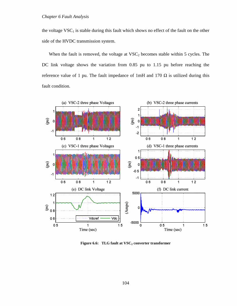
Chapter 6 Fault Analysis
104
the voltage VSC1 is stable during this fault which shows no effect of the fault on the other
side of the HVDC transmission system.
When the fault is removed, the voltage at VSC2 becomes stable within 5 cycles. The
DC link voltage shows the variation from 0.85 pu to 1.15 pu before reaching the
reference value of 1 pu. The fault impedance of 1mH and 170 Ω is utilized during this
fault condition.
Figure 6.6: TLG fault at VSC2 converter transformer

Chapter 6 Fault Analysis
105
6.4 Fault at DC transmission system
During the fault in DC transmission system, the DC voltage on the faulted terminal
reduces due to continuous flow of the DC fault current. The DC capacitors also feed this
fault current which depends on the fault impedance. Since DC breakers are not available
to interrupt this fault current so the AC breakers on both the AC systems must be opened
to remove this fault. This process is slow comparatively so the complete system must be
shut down. The detailed analysis of system behavior during DC fault is out of scope of
this thesis.
6.5 Summary
This chapter provides the VSC-HVDC system performance evaluation under different
symmetrical and asymmetrical faults on VSC1 and VSC2 AC filter bus and DC
transmission system. The waveforms for electrical quantities like voltage, current, active
power, reactive power, DC voltage and current are presented and analyzed during
application of faults to understand the behavior of proposed VSC-HVDC transmission
system.

106
Chapter 7
Conclusions and Future work
7.1 Conclusions
The development of VSC in last decade generated tremendous research interest in its
power system applications. The VSC-HVDC uses the IGBTs and SPWM, which makes it
possible to control the magnitude and phase angle of the converter AC output voltage.
This flexibility of control allows for a number of advantages of VSC-HVDC. In order to
fully utilize the capability of the VSC-HVDC, two control algorithms of the VSC-HVDC
are investigated and the performance is tested under different situations in this thesis. The
direct control and vector control strategies which control active power, AC
voltage/reactive power and DC voltage, are presented and evaluated for the VSC-HVDC
transmission system which connects two weak AC grids. The results for both control
techniques show that the system response is fast, high quality AC voltages and currents
can be obtained, and the active and reactive power can be controlled precisely. However,
the direct control suffers from coupling problems between active/reactive power controls.

Chapter 7 Conclusions and Future work
107
The major contributions of this thesis are as follows:
Development of a detailed model of a 2-level, 3-phase, 6-switch VSC which is
used to build VSC-HVDC transmission system. The model includes
representation of valves, snubber circuits, and passive components.
Implementation of SPWM technique for generating firing pulses for VSC
converter.
Implementation of direct control and vector control strategies which includes
design of four different controllers; two controllers at sending end (active power
and AC voltage/reactive power controller) and two controllers at the receiving
end (DC voltage and AC voltage/reactive power).
Design and implementation of VSC-HVDC transmission system connected to
weak AC grids in EMTP-RV in order to understand the operational behavior of it
under steady-state, dynamic and fault operating conditions.
The simulation results for VSC-HVDC model with direct control strategy show the
satisfactory operation during steady-state and dynamic conditions. Due to coupling
between electrical quantities (voltage and currents), changes in one quantity affect the
other quantity which may lead the system to instability during abnormal conditions (i.e.
faults and sudden load changes).
On the other hand, vector control technique implements the feed forward closed loop
control technique so the coupling between electrical quantities is removed. This is a
major advantage of vector control method when compared to direct control method. The

Chapter 7 Conclusions and Future work
108
vector control strategy is implemented with VSC-HVDC and comprehensive simulation
results show that
The system response is of the order of 0.75 s which is comparatively fast.
The active power and reactive powers in both AC systems can be controlled
independently.
During dynamic tests i.e. 25 % negative step in active and reactive power at
VSC1; 25 % positive step in reactive power and 10 % positive step in DC link
voltage at VSC2, the system response is fast and well controlled.
The active power and reactive power reversal analysis shows the bi-directional
transfer of power capability of VSC-HVDC without large oscillations. At the
instant of active power reversal, the DC voltage increases sharply which depends
on the amount of the active power flow.
During asymmetrical faults at VSC1 and VSC2 AC filter buses, DC voltage drops
and shows some oscillation, the effect on the unfaulted AC side depends on the
active power flow during the application of the fault.
Symmetrical 3-phase faults at both AC sides of HVDC link show the satisfactory
operation of the system. The fault impedance is comparatively higher than single
phase and double phase to ground fault.
The fault application on positive pole of DC link shows that the power can still be
transmitted by unfaulted pole of DC link. The DC capacitors play major role
during faults on DC transmission system and provide the necessary voltages
during these conditions.

Chapter 7 Conclusions and Future work
109
The effect of different DC capacitor sizes on active power, reactive power and
DC voltage is also studied which shows that as the capacitor size increases, the
transients in active and reactive power and AC and DC voltages are reduced. The
cost is the limiting factor for the capacitor size employed in actual installations.
7.2 Future work
The following topics emanating from this research are considered for future work:
Study of proposed VSC-HVDC model during the fault applications at AC and DC
systems, in case of a unbalanced AC system.
Design of VSC-HVDC transmission system using multi-level VSC like Neutral
point clamped and Flying capacitor topologies.
Study of VSC-HVDC and its control systems connected to passive network at
receiving end.
Multi-terminal VSC-HVDC system operation and grid integration of renewable
energy sources like wind and solar farms.
Implementation of active AC filters to VSC-HVDC system.

110
References
[1]. HVDC Transmission: yesterday and today, by Willis Long and Stig Nilsson,
IEEE Power and Energy Magazine March/ April 2007.
[2]. Nikolas Flourentzou, Vassitios G. Agelidis, Georgios D.Demetriades, “VSC-
Based HVDC Power Transmission Systems: An Overview,” IEEE Transactions
on Power Electronics, vol. 24, No.3, March 2009.
[3]. B R Anderson, L Xu, K T G Wong, “Topologies for VSC transmission,” AC-DC
Power Transmission, IEEE Conference Publication no. 485 © IEEE 2001,
28-30 November 2001.
[4]. Gregory Reed, Masatoshi Takeda, “Advantages of Voltage Source Converter
based Design concepts for FACTS and HVDC link Applications,” IEEE Power
Engineering Society General Meeting 2003, vol. 3.
[5]. K. Erikson, “Operational experience of HVDC light,” Seventh International
Conference on AC-DC Power Transmission pp. 205-210, November 2001.
[6]. Jih-sheng Lai, Fang Zheng Peng, “Multilevel converters-A new breed of power
converters,” IEEE Transactions on Industry Applications, vol.32 No.3, May/June
1996.
[7]. D.M. Larruskain, I. Zamora, A.J. Mazón, O. Abarrategui, J. Monasterio,
“Transmission and Distribution Networks: AC versus DC,” Published in May
2005, by Solarec Egypt, Egyptian Solar Research Center.
[8]. Johan Setreus, Lina Bertling, “Introduction to HVDC Technology for reliable
Electrical Power Systems,” in Proc.10th
International Conference on
Probabilistic Methods applied to Power Systems, 2008 pp: 1-8.
[9]. Björn Jacobson, Paulo Fischer, De Toledo, Gunnar Asplund, “500 Mw City
Center In feed with Voltage Source Converter Based HVDC,” 40th
Meeting of
Study Committee B4 and Colloquium on Role of HVDC, FACTS and Emerging
Technologies in Evolving Power Systems, Bangalore, India, July 2005.
[10]. S. Cole, D. Van Hertem, I. Pardon and R. Belmans, “Randstad HVDC: A Case
Study of VSC HVDC Bulk Power Transmission in a Meshed Grid,” Security And
Reliability Of Electric Power Systems CIGRE Regional Meeting, June 18-20,
2007 / Tallinn, Estonia.
[11]. Guanjun Ding, Ghangfu Tang, Zhiyuan He and Ming Ding, “New Technologies
of Voltage Source Converters (VSC) for HVDC Transmission System based on
VSC,” IEEE Power and Energy Society General Meeting - Conversion and
Delivery of Electrical Energy in 21st Century, 2008.

111
[12]. ADSP-21990: Reference frame conversions © Analog devices Inc, January 2002.
[13]. Guibin Zhang, Zheng Xu, Ye Cai, “An equivalent model for simulating VSC
based HVDC,” Transmission and Distribution Conference and Exposition, 2001
IEEE/PES, vol. 1, pp: 20-24.
[14]. Guibin Zhang, Zheng Xu, “Steady-state model for VSC based HVDC and its
controller design,” IEEE Power Engineering Society Winter Meeting 2001,
pp: 1085-1090.
[15]. Wang Yan, Zhao Shu-Zhen, Huangfu Cheng, Ruan Jiang-Jun, “Dynamic model
and control of voltage source converter based HVDC,” IEEE Power and Energy
Engineering Conference 2009, APPEEC 2009, pp.1-5, 2009.
[16]. Parkhideh B., Bhattacharya S., “A practical approach to controlling the back to
back voltage source converter system,” 34th
Annual Conference of IEEE on
Industrial Electronics, 2008, IECON 2008, pp: 514-519.
[17]. Yin Ming, Li Gengyin, Li Guangkai, Liang Haifeng, Zhou Ming, “Modeling of
VSC-HVDC and its active power control scheme,” International Conference
on Power System Technology, POWERCON 2004, Singapore,21-24
November 2004.vol. 2,pp. 1351-1355.
[18]. Gengyin Li, Ming Yin, Ming Zhou, Chengyong Zhao, “Modeling of VSC- HVDC
and control strategies for supplying both active and passive systems,” IEEE
Power Engineering Society General Meeting, 2006.
[19]. M.M.Zakaria Moustafa, S.Filizadeh, “Electromagnetic transient simulation of a
back-to-back voltage source converter based transmission scheme,” Canadian
Conference on Electrical and Computer Engineering 2007, pp.1570-1573.
[20]. M.M.Zakaria Moustafa, S.Filizadeh, “Simulation of a VSC transmission scheme
supplying passive load,” 34th
Annual conference of IEEE on industrial
electronics, 2008, pp.942-946.
[21]. Cuiqing Du., Sannino A, Bollen M.H.J., “Analysis of the control algorithms of
Voltage-Source Converter HVDC,” Power Tech 2005, IEEE Russia. Publication
year: 2005, page(s):1-7.
[22]. Chandra Bajracharya, Marta Molinas, Jonare Suul,Tore M Undeland,
“Understanding of tuning techniques of converter controllers for VSC-
HVDC,” NORPIE 2008, Nordic Workshop on Power and Industrial Electronics,
June 9-11,2008.
[23]. Temesgen M.Haileselassie, Marta Molinas, Tore Undeland, “Multi-terminal
VSC-HVDC system for integration of offshore wind farms and green
112
electrification of platforms in the north sea,” NORPIE 2008, Nordic workshop on
power and industrial electronics, June 9-11, 2008.
[24]. Ahmed Mahjoub, Ravindra Mukerjee, “Modeling of controller for voltage
sourced converter based HVDC transmission system,” 2nd
IEEE International
Conference on Power and Energy (PECON 08), December 1-3, 2008, Johor
Baharu, Malaysia.
[25]. S. Douangsyla, P. Indarack, A. Kanthee, M. Kando, S. Kittiratsatcha and V.
Kinnares, “Modeling for PWM voltage source converter controlled power
transfer,” Intl. Symposium on Communications and Information Technologies
2004, Sapporo, Japan, October 26-29, 2004.
[26]. D.Jovcic, L.A.Lamont, L.Xu, “VSC transmission model for analytical studies,”
IEEE Power Engineering Society General Meeting 2003, Vol.3, 2003.
[27]. K.R.Padiar, Naresh Prabhu, “Modeling, control design and analysis of VSC based
HVDC transmission systems,” International Conference on Power System
Technology 2004 POWERCON 2004, Singapore, 21-24 November 2004.
[28]. Peter W. Lehn, Stephne Podrucky, “Small Signal modeling of Power Electronics
Converters with Resonant Controllers,” International Conference on Power
System Transients IPST 2009, Kyoto, Japan, June 3-6, 2009.
[29]. Jiuping Pan, Reynaldo Nuqui, Le Tang, Per Holmberg, “VSC-HVDC Control and
Application in Meshed AC Networks,” IEEE Power Engineering Society General
Meeting, Pittsburgh, Pennsylvania, July 20-24, 2008.
[30]. Masoud Karimi-Ghartemani and M.Reza Iravani, “A Nonlinear Adaptive Filter
for Online Signal Analysis in Power Systems: Application,” IEEE Transactions
on Power Delivery, Vol.17, No.2, April 2002.
[31]. Vladimir Blasko, and Vikram Kaura, “A New Mathematical Model and Control
of a Three-Phase AC–DC Voltage Source Converter,” IEEE Transactions on
Power Electronics, Vol. 12, No. 1, January 1997, page(s): 116-123.
[32]. Bhim Singh, B. K. Panigrahi, and D. Madhan Mohan, “Voltage Regulation and
Power Flow Control of VSC Based HVDC System,” IEEE International
Conference on Power Electronics, Drive and Energy Systems, PEDES 2006.
[33]. Sonali Dasgupta and Gayatri Agnihotri, “A Control Strategy for a VSC HVDC
System in steady state response,” International Conference on Advances in
Computing, Control, and Telecommunication Technologies, ACT 2009.

113
[34]. Tatsuhito Nakajima, Shoichi Irokawa, “A Control System for HVDC
Transmission by Voltage Sourced Converters,” IEEE Power Engineering Society
Summer Meeting 1999, Publication Year: 1999 , Page(s): 1113 - 1119 vol.2
[35]. Mariusz Cichowlas, Marian P.Kazmierkowski, “Comparison of current control
techniques for PWM rectifiers,” Proceedings of IEEE International
Symposium on Industrial Electronics, 2002.ISIE 2002. Publication Year: 2002,
Page(s): 1259 - 1263 vol.4.
[36]. B. Jacobson, Y. Jiang-Hafner, P. Rey, G. Asplund , “HVDC with Voltage Source
Converters and Extruded cables for up to ±300 kV and 1000MW,” B4-105,
CIGRE, Paris, France 2006.
[37]. F. Schettler, H. Huang, N. Christl, “HVDC transmission system using Voltage
Source Converters-Design and Applications,” IEEE Power Engineering Society
Summer Meeting, 2000, pp: 715-720.
[38]. Joerg Dorn, Hartmut Huang, Dietmar Retzmann, “Novel Voltage-Sources
Converters for HVDC and FACTS Applications,” CIGRE 314, Osaka 2007.
[39]. Michael Bahrman, Abdel-Aty Edris, Rich Haley, “Asynchronous Back-to-Back
HVDC link with Voltage Source Converters,” Presented at Minnesota Power
Systems Conference, Nov 1999, USA.
[40]. Gunnar Asplund , Kjell Eriksson, Hongbo Jiang, Johan Lindberg, Rolf Pålsson
and Kjell Svensson, “DC Transmission Based On Voltage Source Converters,”
International Conference on Large High Voltage Electric Systems, CIGRE 98, vol
4, Paris, France, 1998.
[41]. Stefen G. Johansson, Gunnar Asplund, Erik Jansson and Roberto Rudervall,
“Power System Stability benefits with VSC-DC Transmission Systems,” B4-204,
CIGRE Session, 2004.
[42]. Chang Hsin Chien, Richard W.G. Bucknall, “Analysis of Harmonics in subsea
power transmission cables used in VSC-HVDC Transmission system operating
under steady-state conditions,” IEEE Transactions on Power Delivery, vol.
22,Issue 4, 2007, page(s): 2489-2497.
[43]. Rolf Grunbaum, “Voltage source converters for maintaining power quality and
stability in power distribution,” European Conference on Power Electronics and
Applications, EPE 2005.
[44]. A.Petersson, A.Edris, “Dynamic Performance of the Eagle Pass Back-to-Back
HVDC Light Tie, AC-DC Transmission,” 28-30 November 2001, Conference
Publication No. 485, IEE 2001.

114
[45]. F. Schettler H. Huang N. Christl, “HVDC Transmission Systems using Voltage
Sourced Converters -Design and Applications,” IEEE Power Engineering Society
Summer Meeting, 2000, pp: 715-720.
[46]. Dr. Vijay K. Sood, HVDC and FACTS controllers, 1st ed., New York: KLUWER
Academic Publishers, 2004.
[47]. Chan-Ki Kim, Vijay K. Sood, Gil-Soo Jang, Seong-Joo Lim and Seok-Jin Lee,
HVDC TRANSMISSION Power Conversion Applications in Power Systems,
1st ed., Singapore: John Wiley & Sons (Asia) Pte Ltd, 2009.
[48]. Ned Mohan, Tore M.Undeland and W.P.Robbins, Power Electronics:
Converters, Applications and Design, 2nd
ed., New York, NY: John Wiley and
Sons Inc, 1995.
[49]. Muhammad H.Rashid, Power Electronics Circuits, Devices, and Applications,
3rd
ed., New Jersey: Pearson Prentice Hall, 2004.
[50]. N.G.Hingorani and L.Gyugyi, Understanding FACTS: Concepts and
Technology of Flexible AC Transmission Systems, New York: IEEE Press, 2000.
[51]. Amirnaser Yazdani and Reza Iravani, Voltage-Sourced Converters in Power
Systems, 1st ed., New Jersey: Wiley, 2010.
115
Appendix A
Per Unit Calculations
The VSC-HVDC transmission system modeled in this thesis is converted in per unit. The
following calculations are given for the conversion to per unit.
Sb = Nominal three phase apparent power of the AC network
= 100 MVA
Vb = Nominal peak phase voltage of AC network
= where is line-to-line RMS voltage
Vb = 187.795 kV
Ib = Nominal peak phase current
=
= 355 Amps
Zb = Base AC impedance
=

116
=529 Ω
ωb = Base angular frequency
= 377 rad/sec
The per unit presentation at the DC side is achieved as follows:
As, = and then the power balance is given by,
The base value for the DC voltage is chosen as,
Then by the power balance equation as above,
And
= 1410.66 Ω
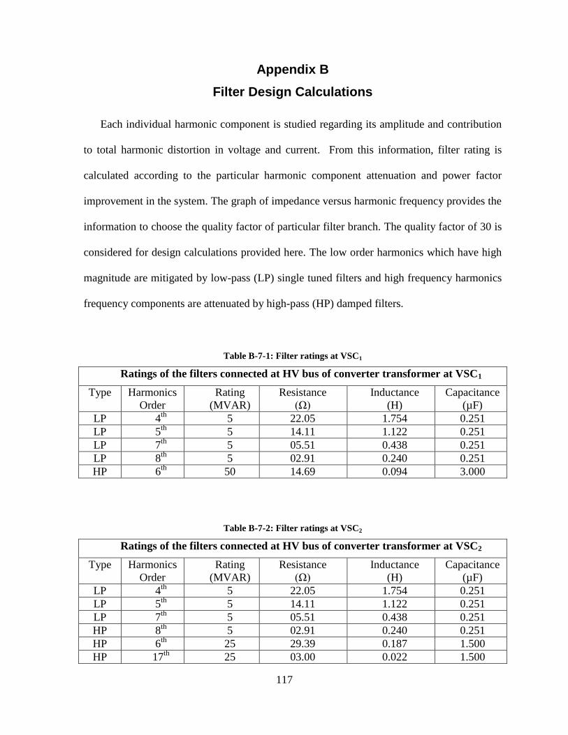
117
Appendix B
Filter Design Calculations
Each individual harmonic component is studied regarding its amplitude and contribution
to total harmonic distortion in voltage and current. From this information, filter rating is
calculated according to the particular harmonic component attenuation and power factor
improvement in the system. The graph of impedance versus harmonic frequency provides the
information to choose the quality factor of particular filter branch. The quality factor of 30 is
considered for design calculations provided here. The low order harmonics which have high
magnitude are mitigated by low-pass (LP) single tuned filters and high frequency harmonics
frequency components are attenuated by high-pass (HP) damped filters.
Table B-7-1: Filter ratings at VSC1
Ratings of the filters connected at HV bus of converter transformer at VSC1
Type
Harmonics
Order
Rating
(MVAR)
Resistance
(Ω)
Inductance
(H)
Capacitance
(µF)
LP 4th
5 22.05 1.754 0.251
LP 5th
5 14.11 1.122 0.251
LP 7th
5 05.51 0.438 0.251
LP 8th
5 02.91 0.240 0.251
HP 6th
50 14.69 0.094 3.000
Table B-7-2: Filter ratings at VSC2
Ratings of the filters connected at HV bus of converter transformer at VSC2
Type
Harmonics
Order
Rating
(MVAR)
Resistance
(Ω)
Inductance
(H)
Capacitance
(µF)
LP 4th
5 22.05 1.754 0.251
LP 5th
5 14.11 1.122 0.251
LP 7th
5 05.51 0.438 0.251
HP 8th
5 02.91 0.240 0.251
HP 6th
25 29.39 0.187 1.500
HP 17th
25 03.00 0.022 1.500
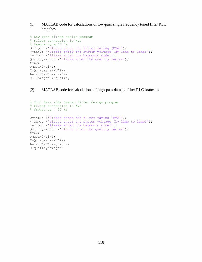
118
(1) MATLAB code for calculations of low-pass single frequency tuned filter RLC
branches
% Low pass filter design program % Filter connection is Wye % frequency = 60 Hz Q=input ('Please enter the filter rating (MVA)'); V=input ('Please enter the system voltage (kV line to line)'); n=input ('Please enter the harmonic order'); Quality=input ('Please enter the quality factor'); f=60; Omega=2*pi*f; C=Q/ (omega*(V^2)) L=1/(C*(n*omega)^2) R= (omega*L)/quality
(2) MATLAB code for calculations of high-pass damped filter RLC branches
% High Pass (HP) Damped Filter design program % Filter connection is Wye % frequency = 60 Hz
Q=input ('Please enter the filter rating (MVA)'); V=input ('Please enter the system voltage (kV line to line)'); n=input ('Please enter the harmonic order'); Quality=input ('Please enter the quality factor'); f=60; Omega=2*pi*f; C=Q/ (omega*(V^2)) L=1/(C*(n*omega) ^2) R=quality*omega*L

119
Appendix C
ABC-dq Conversions
Figure 7: ABC to dq conversion block modeling in EMTP-RV
Figure C 1 shows the modeling of ABC to dq conversion in EMTP-RV. The introduction
of reference frames in the analysis of electrical machines has turned out not only to be useful
in their analysis but also has provided a powerful tool for the implementation of sophisticated
control techniques. The significant breakthrough in the analysis of three-phase AC machines
was the development of reference frame theory. Using these techniques, it is possible to
transform the phase variable machine description to another reference frame. By appropriate
choice of the reference frame, it is possible to simplify considerably the complexity of the
mathematical machine model. These techniques are initially developed for the analysis and
simulation of AC machines; they are now invaluable tools in the digital control. These digital
control techniques are now extended for control of currents also. Over the years, many
different reference frames have been proposed for the analysis but the most commonly used
ones are the stationary reference frame and the rotor reference frame.
f(u)1
f(u)1
Fm6
f(u)1
Fm7
f(u)1
Fm8
f(u)1
f(u)1 f(u)
a
b
cf(u)
1
2
3
4
5
6
f(u)
1
2
3
4
5
6
Fm13
f(u)
1
2
3
d
q
z
SUM1
2
t
cos0
cos1
cos2
sin0
sin1
sin2
d
q
a
b
c
z
omega_t
t
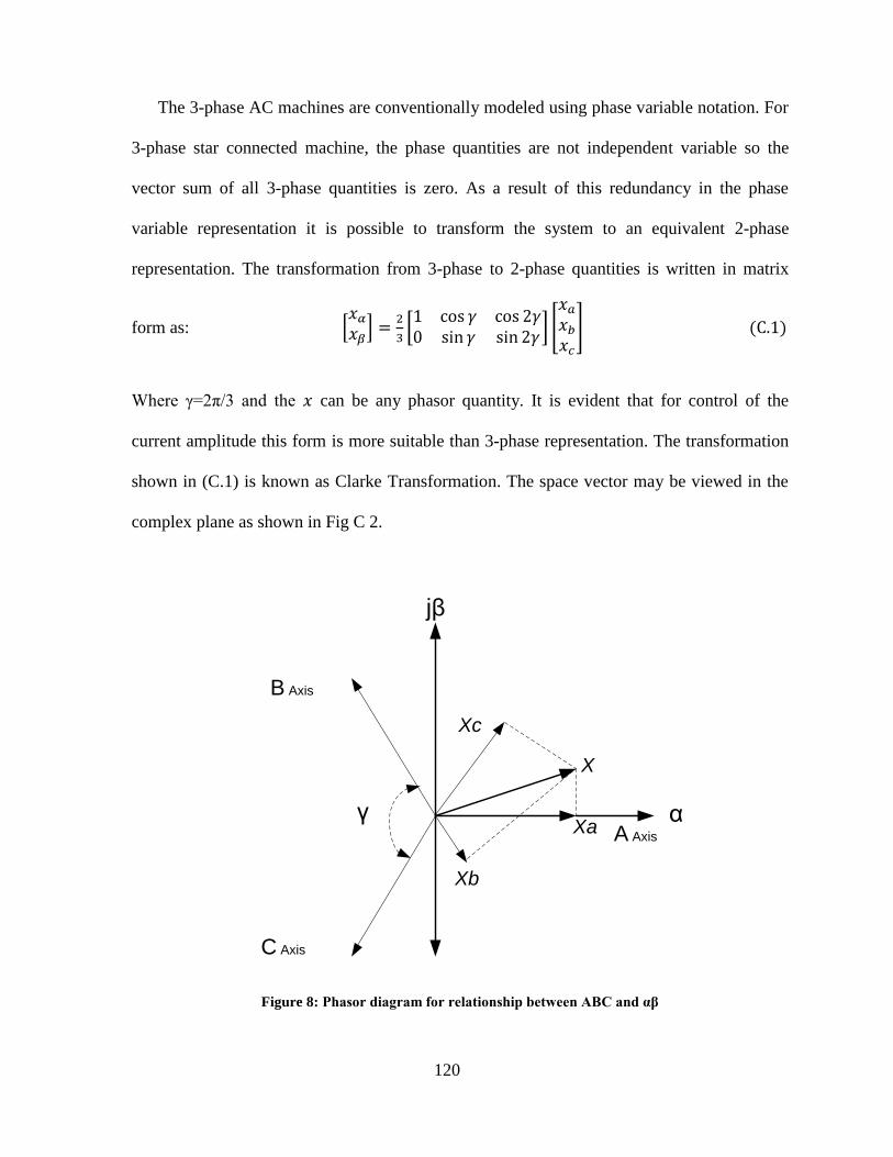
120
The 3-phase AC machines are conventionally modeled using phase variable notation. For
3-phase star connected machine, the phase quantities are not independent variable so the
vector sum of all 3-phase quantities is zero. As a result of this redundancy in the phase
variable representation it is possible to transform the system to an equivalent 2-phase
representation. The transformation from 3-phase to 2-phase quantities is written in matrix
form as: (C.1)
Where γ=2π/3 and the can be any phasor quantity. It is evident that for control of the
current amplitude this form is more suitable than 3-phase representation. The transformation
shown in (C.1) is known as Clarke Transformation. The space vector may be viewed in the
complex plane as shown in Fig C 2.
Xa
X
α
jβ
Xb
Xc
A Axis
B Axis
C Axis
γ
Figure 8: Phasor diagram for relationship between ABC and αβ

121
In case of AC machine theory, the stator space vectors are complex quantities defined in
a reference frame whose real axis is fixed to the magnetic axis of the stator winding. The
corresponding quantities defined for the rotor circuit of a 3-phase AC machine are similarly
stated in a reference frame fixed to the rotor. In the analysis of electrical machines, it is
necessary to adopt a common reference frame for both the rotor and the stator. The second
transformation known as a vector rotation is formulated that rotates space vector quantities
through a known angle. The space vector in this new reference frame is written in matrix
form as:
(C.2)
Where the angle the angle by which the vector rotation is done. This transformation is
called Park’s transformation. The relationship of the real and imaginary components of the
current space vector in the original stationary two-axis reference frame and the new rotating
reference frame is shown in the Fig 63.

122
Xα
X
α
jβ
Xb
Stationary Real
Axis
d
jq
Xβ
Xq
Xd
Stationary
Imaginary Axis
Rotating
Imaginary Axis Rotating Real
Axis
θ
ω
Figure 9: Phasor diagram for relationship between ABC, dq and αβ quantities
From above discussion, it can be said that a balanced 3-phase system in phase variables
may be transformed to an equivalent 2-axis representation that is independent of the angular
position by applying a three-phase to two-phase transformation followed by a vector rotation
by the angular position of the phase quantities.
The two transformations can be combined in one step using following matrix equation.
(C.3)
Equation C.3 can be used for the conversion of ABC-quantity in to dq-quantity directly.

123
Appendix D
EMTP-RV: An Overview
EMTP-RV was originally developed by the Bonneville Power Administration (BPA),
Portland, Oregon. The present version was developed at IREQ, Hydro-Quebec under the
agreement with the Direct Coordination Group (DCG). This software is widely used in power
utilities, research institutes and academic institutions for transients simulation studies around
the world, and is a circuit based power system simulator. This thesis used the software for the
modeling and study of 2 levels, 6 switches VSC based HVDC transmission system. The
EMTP-RV is the enhanced computational engine and EMTP Works is its new Graphical
User Interface (GUI).
Power system networks can be modeled using EMTP-RV to represent practical systems
and large numbers of models are available in EMTP-RV for study purpose. These models
can be used for the steady state and transient state phenomenon simulation in power
networks. The power network can be modeled using voltage or current sources, machines,
multiphase circuits, distributed or lumped parameter line models and switches. The simulated
model can be used to represent a specified power system. There are different subroutines
available in EMTP-RV that solve the mathematical equations and provide solutions to such
models. Another advantage of the EMTP-RV is that it can handle very large and complex
power system networks. Its uses include switching and lighting surge analysis, insulation
coordination and power electronic applications in power systems. Further information about
EMTP-RV can be obtained from the website www.emtp.com.

124
Appendix E
List of Publications
1. As a part of this research, the following research paper has been accepted by IEEE
Electrical Power and Energy Conference (EPEC 2010) at Halifax, Nova Scotia,
August 25-27, 2010. Hiteshkumar Patel and V.K. Sood, “Modeling of Voltage
Source Converter based HVDC system in EMTP-RV,”
2. As a part of this research, the following paper is going to be submitted to an
International conference. Hiteshkumar Patel and V.K. Sood, “Comparison of direct
control and vector control methods for Voltage Source Converter based HVDC
transmission system,”


![Distributed PLL-based Control of Offshore Wind Turbines ...€¦ · distance offshore wind power transmission [1]-[7]. To date, voltage-source-converter based HVDC (VSC-HVDC) links](https://img.pdfslide.us/doc/110x75/5ea2b21262bde80d0215fab0/distributed-pll-based-control-of-offshore-wind-turbines-distance-offshore-wind.jpg)