Embed Size (px)
Citation preview

MODELING OF DRAIN CURRENT FOR GRAPHENE CHANNEL G4FET AND GATE-ALL-AROUND
MOSFET
A thesis submitted in partial fulfillment of the requirements for the degree of
Master of Science in Electrical and Electronic Engineering
by
Md. Rakibul Alam Student No: 1015062260F
Department of Electrical and Electronic Engineering
Bangladesh University of Engineering and Technology
December 2018

i

ii
Declaration
It is hereby declared that this thesis or any part of it has not been submitted elsewhere for the
award of any degree or diploma.
Signature of the Candidate
____________________________________
(Md. Rakibul Alam)

iii
To my beloved family

iv
Acknowledgment
All praise goes to the Almighty for giving me the patience and drive required to complete my
M.Sc. research and finish the dissertation in due time.
I would begin by heartily thanking my thesis supervisor Hamidur Rahman, Associate
Professor, Department of Electrical and Electronic Engineering (EEE), Bangladesh
University of Engineering and Technology (BUET), for his generous help, edifying
suggestions and well-definedguidance throughout the thesis work. I feel grateful to him for
giving mesufficient freedom and having faith in my capabilities, which made the research
work very much enjoyable for me. His passion and dedication to academic research has
motivated me to push my boundaries harder and excel at my research work, which I believe
will inspire me to be a better researcher in future days to come.
I want to express my gratitude to Tyafur Rahman Pathan, Lecturer, Department of Electrical
and Electronic Engineering (EEE), Green University, Bangladesh, for his kind help with the
discussion on MOSFET and COMSOL with MATLAB. I also want to thank Shafat Jahangir,
PhD student, Graduate Research Assistant, Department of Electrical Engineering and
Computer Science (EECS), University of Michigan, for his sincere help on G4FET.
I would like to thank my family anddedicate my thesis to them. They have been the
encouragement behind my every successful endeavor. This thesis work is not an exception
and this would not have been completed without their constant support and inspiration.
Finally, I put forward my humble gratitude to all my colleagues, friends and well-wishersfor
their help, support and words of encouragement during my research work.

v
Abstract
The structure of Graphene channel Four Gate Field Effect Transistor (G4-FET) and Gate-All-
Around (GAA) MOSFET have been developed in 3D ATLAS simulator of SILVACO in this
thesis. Drain current of Graphene channel G4-FET and GAA MOSFET are calculated and
compared in this study.The performance of the deviceshas also been investigated in this
article. An optimized structure is designed for the performance matrix such as threshold
voltage, Subthreshold Swing (SS), Drain Induced Barrier Lowering (DIBL),
transconductance etc. and the results are compared with existing FET structure in this paper.
vi
Table of Contents
Approval ............................................................................ Error! Bookmark not defined.
Declaration....................................................................................................................... i
Acknowledgment ........................................................................................................... iv
Abstract ............................................................................................................................v
Table of Contents .......................................................................................................... vi
List of Figures ............................................................................................................... vii
List of Abbreviations .................................................................................................. viii
List of Symbols .............................................................................................................. ix
1 Introduction ............................................................................................................1
1.1 Literature Review.............................................................................................. 2 1.2 Thesis Objectives .............................................................................................. 6 1.3 Thesis Organization .......................................................................................... 6
2 Structure and Device Dimension of G4-FET and GAA MOSFET and Solving
Method .............................................................................................................................7
2.1 Structure and Device Dimension of G4-FET and GAA MOSFET ................... 7 2.2 Solving Method ............................................................................................... 11
3 Results and Discussions .......................................................................................12
3.1 Current-Voltage Characteristics ...................................................................... 12 3.2 Threshold Voltage ........................................................................................... 14 3.3 Subthreshold Swing (SS) / Subthreshold Slope (SS) ...................................... 16
3.4 Drain Induced Barrier Lowering (DIBL) ........................................................ 18 3.5 Transconductance ........................................................................................... 18
4 Conclusion ............................................................................................................21
4.1 Summary ......................................................................................................... 21 4.2 Suggestions for Future Work .......................................................................... 21
References ......................................................................................................................22
Appendix A ....................................................................................................................25
vii
List of Figures
Figure 2.1 (a) n-Graphene channel G4-FET structure (b) Cross-section of n-Graphene
channel G4-FET ...................................................................................................... 8
Figure 2.2 (a) n-Graphene channel cubical GAA MOSFET structure (b) Cross-section
of n-Graphene channel cubical GAA MOSFET ..................................................... 9
Figure 2.3 (a) n-Graphene channel cylindrical GAA MOSFET structure (b) Cross-
section of n-Graphene channel cylindrical GAA MOSFET ................................. 10
Figure 3.1 Drain Current vs Drain Voltage at V_g = 0V, 0.2V 0.4V, 0.6V, 0.8V, 1V
(a) for n-Graphene channel G4-FET, (b) for n-Graphene channel cubical GAA
MOSFET, (c) for n-Graphene channel cylindrical GAA MOSFET ..................... 13
Figure 3.2 Threshold voltage calculation at V_d = 0.1 V and V_d = 0.8 V (a) for n-
Graphene channel G4-FET, (b) for n-Graphene channel cubical GAA
MOSFET, (c) for n-Graphene channel cylindrical GAA MOSFET ..................... 15
Figure 3.3 Subthreshold Swing calculation at V_d = 0.1 V and V_d = 0.8 V (a) for n-
Graphene channel G4-FET, (b) for n-Graphene channel cubical GAA
MOSFET, (c) for n-Graphene channel cylindrical GAA MOSFET ..................... 17
Figure 3.4 Transconductance at V_d = 0.1 V and V_d = 0.8 V (a) for n-Graphene
channel G4-FET, (b) for n-Graphene channel cubical GAA MOSFET, (c) for
n-Graphene channel cylindrical GAA MOSFET .................................................. 20

viii
List of Abbreviations
FET Field-effect transistor
MOSFET MetalOxideSemiconductor FieldEffect Transistor
G4-FET Four Gate Field Effect Transistor
GAA Gate-All-Around
SS Subthreshold Swing
DIBL Drain Induced Barrier Lowering
BJT Bipolar junction transistor
SOI Silicon on insulator
DGMOSFET Double Gate MOSFET
GAA-CNFET GAA Carbon Nanotube FET
CGAA Cylindrical GAA
DAA Depletion-all around

ix
List of Symbols
𝑁𝐴 Doping density of junction gate
𝑁𝐷 Channel doping density
∈0 Permittivity of free space
∈𝑟 Relative permittivity
Eg Bandgap
µn Electron Mobility
µp Hole Mobility

1
1
Introduction
Transistors are the main components of all modern electronic devices [1]. In 1950‟sTransistor
began to replace vacuum tubes and produced the integrated circuit and microprocessor which
is the heart of semiconductor industry [2]. On 10 December 1956 Shockley, Bardeen and
Brattain were awarded the Nobel Prize in physics for “investigations on semiconductors and
the discovery of the transistor effect” [2].Bipolar junction transistor (BJT) was invented by
W.B. Shockley at the Bell Telephone Laboratories in 1948 [3].Development of the Nano-
electronics technology replaced BJT by MetalOxide Semiconductor Field Effect Transistor
(MOSFET) which was invented in 1960‟s[4].
The planar bulk-silicon MOSFET has been used in the semiconductor industry over the last
40 years.The scaling of bulk MOSFETs became increasingly difficult for gate lengths below
32nm[4].Partially depleted Silicon on insulator (SOI) MOSFET and fully depleted SOI
MOSFET has a layered silicon-insulator-silicon substrate instead of conventional silicon
substrates to reduce parasitic device capacitance to improve circuit performance[4].
The SOI technology has the possibility of having more than one gate for eachtransistor due to
the presence of two oxide layers. Because of the twooxide layers, the number of gates can be
extended to four for SOI technology with twojunction gates in addition to the two oxide
gates.
Double Gate MOSFET (DGMOSFET) with two oxide gates utilizes the two oxide layers as
independent gates to control conduction channel.The transistor with four gates is called a
Four Gate Field Effect Transistor (G4FET) which is introduced in 2002 [5].Gate-All-Around
(GAA) MOSFET is a device which is developed toprovide high performancessuch as high
on-off current ratio, reduced delayand short channel effect, lower Drain Induced Barrier
Lowering (DIBL) etc.It has a good future scopeto be used in the ultra-scale integration.
The International Roadmap for Semiconductors industryshows an evolution from bulk to
silicon-on-insulator (SOI) and then to multiple-gate MOSFET for high-performance digital
Chapter

2
integrated circuits[6]. The continuous scaling of Gate-All-Around (GAA) silicon nanowire
Field Effect Transistor (FET) [7], [8] shows better control of short channel effect over other
structures [9] due to their gate controllability, low leakage, high on-off ratio and carrier
transport property [10].
1.1 Literature Review
Z. Chen et al. [11] discusses the fabrication process and device measurements of GAA
Carbon Nanotube FET (GAA-CNFET) with an „Ω‟ shaped model. They also comment about
how much charges in the gate oxide are responsible for the nonideal device performance.
S. Garget al. [12] claims the calculation of threshold voltage using center potential and the
calculation of the effect of device parameters on threshold voltage of cylindrical GAA
MOSFET.
T. K. Sachdevaet al. [13] analyzes the electrical characteristics of cylindrical GAA (CGAA)
MOSFET at 50nm channel length (Lg) and 10nm channel thickness (tsi). Various electrical
characteristics such as ON current (ION), subthreshold leakage current (IOFF), the threshold
voltage (Vth), DIBL are calculated and analyzed at various device design parameters.
K. P. Pradhan et al. [14] proposes an analytical threshold voltage model for a cylindrical
gate-allaround (CGAA) MOSFET by solving the 2-D Poisson‟s equation in the cylindrical
coordinate system. They claim that the calculation of threshold voltage using center potential
is more accurate rather than the calculation from surface potential.
Saeed et al. [15] proposes an analytical model to calculate gate capacitance and drain current
of rectangular GAA nanowire MOSFET with group III-V channel (In0.53Ga0.47As). Using the
proposed model for gate capacitance in strong inversion region and drain current together
with semi-numerical ballistic MOSFET model, the performance of In0.53Ga0.47As with
channel doping density of2×1016cm-3 GAA MOSFET is examined.
K. S.Kiranet al.[16] analyzes a 3-D model of GAA MOSFET with different gate materials of
group III-V (InGaAs, GaAs, InP) and studies electrical characteristics of GAA MOSFETs.

3
S. Jahangiret al. [17],[18],[19]discusses about the effect of gate bias on the location and size
of the conducting channel in depletion-all around (DAA) operation of SOI four-gate
transistor (G4-FET).They develop a numerical model for solving 2-D Poisson-Schrödinger
equation in depletion-all-around (DAA) operation of n-channel four gate transistor (G4FET)
by finite element method. They calculate the Ballistic drain current by mode-space approach
using modified Tsu-Esaki equation. They also observe the effect of multiple gate bias on
current-voltage characteristics.
S. Sayed et al. [20], [21]develops an analytical model to determine the 3-D potential
distribution of a fully-depleted silicon-on-insulator (SOI) four-gate transistor (G4-FET).
Using these assumptions andnecessary boundary conditions, the 3-D Poisson‟s equation is
solved to formulate the overall expression of potential distribution and correlated with the
four gates of the device and shows excellent agreement with the charge variation along the
channel.
F. S. Snigdha et al. [22] discusses the conformal mapping technique which is used to model
potential distribution of SOI four gate transistor in sub threshold region. They also
investigatethe potential variation between the MOS gates and junction gates for different
structural parameters.
S. Sayed et al. [23] develops amathematical model to determine the 3-D potential distribution
of a fully-depleted SOIp-channel G4-FET. Using this model, surface potential is studied by
changing various parameters and gate voltages. They also investigate the potential variation
between the MOS gates for different parameters.
J. Y. Songet al. [24]designs gate-all-around (GAA) MOSFETs. Theyoptimize and compare
with that of double-gate MOSFETs.Theydiscuss the optimal ratio of the fin width to the gate
length andinvestigate short-channel effects of GAA MOSFETs. Using three dimensional
simulations, they confirm that short-channel effectsare properly suppressed although the fin
width is the same asthe gate length in GAA MOSFETs. Finally, they compare cubicalchannel
GAA MOSFETs with cylindrical-channel.
H. A. E. Hamid et al. [25] develops an analytical model for the calculation of the threshold
voltage, subthreshold swing and drain-induced barrier lowering(DIBL) of undoped
4
cylindrical GAA MOSFETs based on an analytical solution of 2-D Poisson‟sequation (in
cylindrical coordinates) in which the mobile chargeterm has been included. Using this model,
they investigate threshold voltage,DIBL and subthreshold swing sensitivities to channel
length andchannel thickness.
B. Debnath et al. [26] develops a simulation model for SOI G4-FET by Silvaco/Atlas 3-D
simulator which incorporates non-ideal effects like concentration dependent mobility,
Shockley-Read-Hall recombination, Auger recombination, bandgapnarrowing effect. Using
this model, they measure the different parameters for different biasing conditions.
M. S. Islam et al. [27] studies an analytical model for SOI G4-FET by Silvaco/Atlas 3-D
simulator to calculate the threshold voltage. They also investigate the threshold voltage
sensitivity on channel lengthvariation by controlling device width (W) and siliconlayer
thickness (tsi).
A. F. M. S. Haq et al. [28] studies a numerical model for thin film SOI p-channel G4-FET by
Silvaco/Atlas 3-D simulator to calculate the potential distribution. They observe
theperformance of varying diff erent parameters like length, width,silicon thickness and gate
biasing between lateraljunction gates and between top and bottom gates.
S. L. Noor et al. [29] develops a three dimensional model of SOI p-channel fourgate
transistor using device simulator Silvaco/ATLAS. They investigate the threshold voltage for
the device fordifferent biasing condition at the four gates and different physicalparameter like
channel length. They also compare theresults from the analytical model of threshold voltage
ofn-channel four gate transistor to find out whether the analyticalmodel works for p-channel
G4-FET.
H. Mohammadi et al. [30]evaluates the drainbreakdown voltage of n-channel FD-SOI four-
gate MOSFETs using three dimensional solution ofPoisson‟s equation with proper boundary
conditions for thesurface potential and electrical field distribution. This model can predict the
drain breakdown voltage versus biasconditions and device parameters including silicon film
thickness,oxide layer thickness and channel doping concentration.
5
S.Sayed et al. [31] develops a mathematical model to determine thesubthreshold swing of
thin-film fully depleted SOI four-gate transistors using 2-DPoisson‟s equation to calculate the
potential distribution. They investigate the subthreshold swing which isa strong function of
back-surface charge condition and dependon structural parameters of the device.
K. Akarvardar et al. [32] introduces the fully-depleted version of the SOI four-gate transistor
and its characteristics are systematically investigated. They provide a very efficient control of
the front-channel conduction parameters such as threshold voltage, subthresholdswing and
transconductance by the junction-gates regardless the device width.
K. Akarvardar et al. [33] develops a model ofSOI G4-FETto calculate the potential
andthreshold voltage by solving 2D Poisson‟s equation. Using this model, they calculate the
surface potential and threshold voltage as a function of the lateral gate bias and for all
possiblecharge conditions.
S. Sayed et al. [34] proposes a model to analyze the transistor characteristics of fully depleted
SOI four gatefield effect transistors by solving 2-D Poisson‟s equation. This model is used
for the calculationof surface potential and charge densities as a function of all gate biases.
K. Akarvardar et al. [35] introduces the depletion-all-around (DAA) SOI G4-FET. They
investigate the drain current, threshold voltage,DIBL, transconductance, carrier mobility and
subthreshold swing.
B. Jena et al. [36] analyzes the sensitivity of process parameters such as channel length,
channel thickness and gate work function on various performance metrics of an undoped
cylindrical GAA MOSFET. They investigate the electrical characteristics as well as the
analog/RFperformances of undoped GAA MOSFET through device simulator.
M. Khaouaniet al. [37] studies a numerical model of a square structure with single channel
compared to a structure with 4 channels in order to highlight the impact of channel number
on the device‟s DC parameters like as drain current, DIBL, on-off current ratio and threshold
voltage.

6
M. Kumar et al. [38] develops a model of Dual Material Gate(DMG) Schottky-Barrier (SB)
Source/Drain (S/D) GAA MOSFET with conventional DMG-GAA having doped S/D
MOSFET and DMG Junctionless GAAMOSFET. They investigate the RF/Analog
performance such as transconductance, intrinsic gain, cut-off frequency, and on-off current
ratiousing ATLAS-3D DeviceSimulator.
From the literature review, no reports have been made so far about Graphene being used as
the channel for G4-FET and GAA MOSFET. Graphene which has lower relative permittivity
and very higher mobility than silicon can be used as the channel of G4-FET and GAA
MOSFET in an effort to increase the potential distribution and drain current.
1.2 Thesis Objectives
The objectives of this work are:
a. To develop a quantum mechanical numerical model for finding potential distribution
and carrier density for G4-FET and GAA MOSFET with Graphene as the channel.
b. To determine the current-voltage characteristics.
c. To design an optimized structure for the performance matrix such as
transconductance, threshold voltage, Subthreshold Swing (SS), Drain Induced Barrier
Lowering (DIBL), on-off current ratio etc.and compare the results with existing FET
structure.
1.3 Thesis Organization
The entire thesis is organized into four chapters. Chapter 1 briefly discusses about the
revolution of MOSFET, literature review and objectives of the thesis. Chapter 2 discusses
about the structure and device dimension of G4FET and GAA MOSFETandalso discusses
about the solving method. Chapter 3 shows the simulation results and explains different
observations and compares with existing FET structure. Finally, conclusion of this work with
future works are presented in chapter 4.

7
2
Structure and Device Dimension of G4-FET and GAA
MOSFET and Solving Method
This chapter discusses aboutthe structure and device dimension of G4-FET and GAA
MOSFET and solving method.
2.1 Structure and Device Dimension of G4-FET and GAA MOSFET
The G4-FET is a double gate MOSFET consisting oftwo lateral junction-gates (Junction Gate
1 and Junction Gate 2). It has a lateral double-gate MOS consisting of two vertical MOS
gates (top-gate and back-gate). Under appropriate gate bias voltages, the performance and
properties of the device are affected by the presence of inversion layers under MOS gates
because the junction gates are interconnected through the channel. There are two types of
structure of GAA MOSFET: rectangular and cylindrical. InGAA MOSFETs, the gate oxide
and the gate electrodes wrap around the channel region. In this paper, multi-layer Graphene is
used as the channel in G4-FET and GAA MOSFET. ID flows through the Graphene and the
conducting channel surrounded by depletion regions.
In G4-FET device structure (Figure 2.1) considered in this thesis, the channel width and
channel thickness are 10 nm, gate oxide and buried oxide thickness are 1.3 nm, top and
bottom gate thickness are 10 nm. The doping density of junction gate is 𝑁𝐴 = 1 × 10²⁰𝑐𝑚−3
and the channel doping density is 𝑁𝐷 = 1 × 10¹⁷𝑐𝑚−3.
Chapter

8
(a)
(b)
Figure 2.1(a) n-Graphene channel G4-FET structure (b) Cross-section of n-Graphene channel G4-FET
In cubical GAA MOSFET (Figure 2.2) considered in this thesis, the channel width and
channel thickness are taken as 10 nm, surrounding gate oxide thickness is 1.3 nm and
surrounding gate thickness is 10 nm.

9
(a)
(b)
Figure 2.2(a) n-Graphene channel cubical GAA MOSFET structure (b) Cross-section of n-Graphene channel cubical GAA MOSFET
In cylindrical GAA MOSFET (Figure 2.3) considered in the dissertation, the channel
diameter is 10 nm, surrounding gate oxide thickness is 1.3 nm and surrounding gate thickness
is 10 nm.

10
(a)
(b)
Figure 2.3(a) n-Graphene channel cylindrical GAA MOSFET structure (b) Cross-section of n-Graphene channel cylindrical GAA MOSFET
In all the three structures, the gate oxide thickness and gate thicknesses are the same and the
other dimensions are comparable to make the analyses on the same footing. For example, the
channel diameter of cylindrical GAA MOSFET, the channel width and the thickness of
cubical GAA MOSFET and the channel width of G4-FET device structure are all 10 nm.

11
Table 2.1 Device Dimension of G4-FET and GAA MOSFET
Device parameters G4-FET Cubical GAA
MOSFET
Cylindrical GAA
MOSFET
Channel length 30 nm 30 nm 30 nm
Channel width/ Channel
diameter
10 nm 10 nm 10 nm
Channel height/ Channel
diameter
10 nm 10 nm 10 nm
Gate oxide thickness/
surrounding gate oxide
thickness
1.3 nm 1.3 nm 1.3 nm
Buried oxide thickness 1.3 nm - -
Top gate thickness/
surrounding gate thickness
10 nm 10 nm 10 nm
Bottom gate thickness 10 nm - - Junction gates width 20 nm - -
Doping density of junction
gates (p+)
1 × 1020cm−3 - -
Channel doping density (n) 1 × 1017cm−3 1 × 1017cm−3 1 × 1017cm−3
doping density of drain and
source (n+)
1 × 1020cm−3 1 × 1020cm−3 1 × 1020cm−3
2.2 Solving Method
G4-FET and GAA MOSFET are analysed for characteristics curve using 3D ATLAS
simulator of SILVACO. Various models have been used to perform analysis in ATLAS.
Shockley-Read-Hall (SRH) model is used for recombination andLombardi model (CVT) is
used for carrier mobility. The multi-layer Graphene which is used as channel is not included
in the library of SILVACO. So a material is declared as Graphene and defined the parameters
of Graphene.Table 2.2 shows the parameters of Graphene which are used for this work.
Table 2.2Material Parameters of Graphene
Parameters Bandgap,
Eg (eV)
Permittivity Electron Mobility,
µn (cm2/V-s)
Hole Mobility,
µp (cm2/V-s)
Affinity
(kg/mole)
Value 0.5 25 10000 10000 4.248
12
3
Results and Discussions
In this chapter, simulation results are shown and the different observations are explained
using 3D SILVACO/ATLAS and compared with existing FET structure.
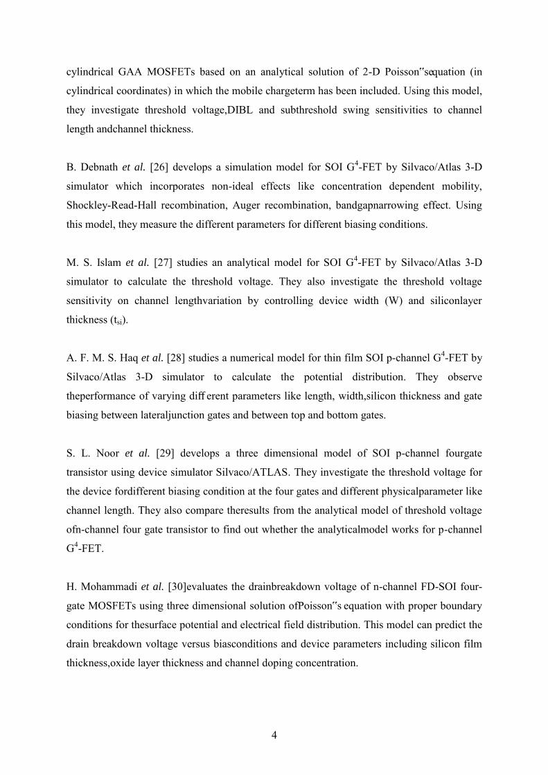
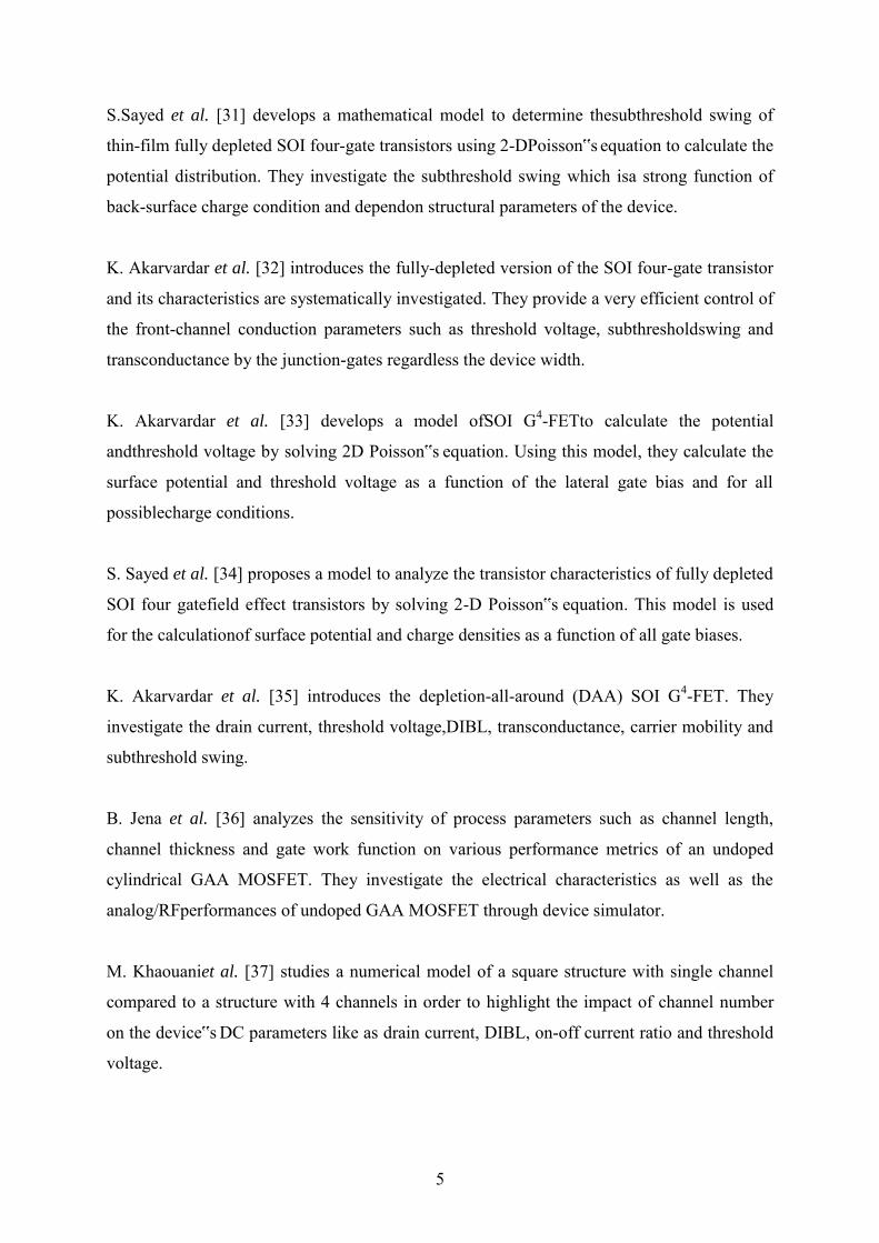
3.1 Current-Voltage Characteristics
Figure 3.1shows the drain current for n-Graphene channel G4-FET and GAA MOSFET.
Drain current increases due to increasing gate bias voltages.
(a)
Chapter
13
(b)
(c)
Figure 3.1Drain Current vs Drain Voltage at V_g = 0V, 0.2V 0.4V, 0.6V, 0.8V, 1V (a) for n-Graphene channel
G4-FET, (b) for n-Graphene channel cubical GAA MOSFET, (c) for n-Graphene channel cylindrical GAA
MOSFET

14
Table 3.1 shows the comparison of maximum Drain current between G4-FET and GAA
MOSFET at V_g = 0.2V. Drain current of n-Graphene channel cubical GAA MOSFET is
larger than other two structures.
Table 3.1 Comparison of maximum Drain current between G4-FET and GAA MOSFET
Properties n-Graphene
channel G4-FET
n-Graphene channel
cubical GAA
MOSFET
n-Graphene channel
cylindrical GAA
MOSFET
Maximum
Drain Current
at V_g = 0.2 V
2.76 µA 23.51 µA 22.80 µA
3.2 Threshold Voltage
Figure 3.2shows the calculation of threshold voltage for n-Graphene channel G4-FET and
GAA MOSFET for different drain voltages.Table 3.2 shows the values of the threshold
voltage. The threshold voltage decreases with increasing drain voltage.
(a)

15
(b)
(c)
Figure 3.2Threshold voltage calculation at V_d = 0.1 V and V_d = 0.8 V(a) for n-Graphene channel G4-FET, (b)
for n-Graphene channel cubical GAA MOSFET, (c) for n-Graphene channel cylindrical GAA MOSFET
16
Table 3.2 Comparison of threshold voltage between G4-FET and GAA MOSFET
Properties n-Graphene
channel G4-
FET
n-Graphene channel
cubical GAA
MOSFET
n-Graphene channel
cylindrical GAA
MOSFET
Threshold
voltages,
V_th
V_d = 0.1 V -0.1378 V -0.1295 V -0.1520 V
V_d = 0.8 V -0.1396 V -0.1456 V -0.1660 V
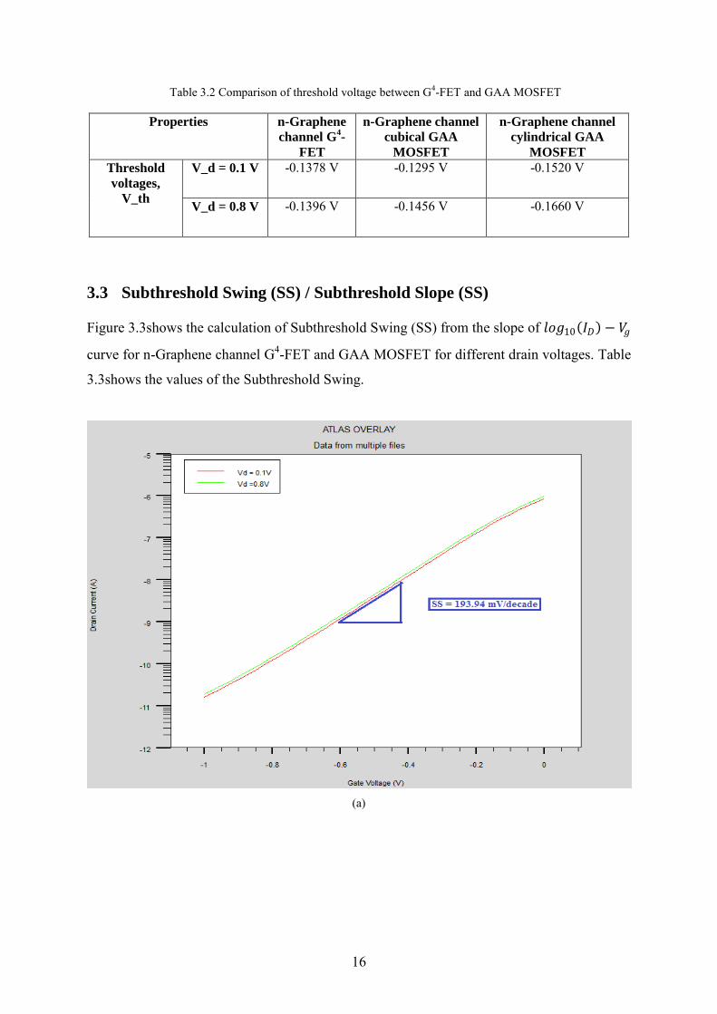
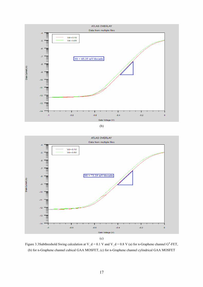
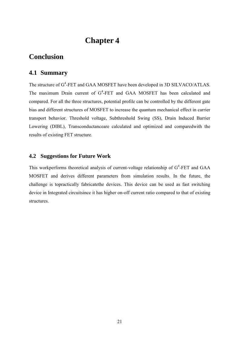
3.3 Subthreshold Swing (SS) / Subthreshold Slope (SS)
Figure 3.3shows the calculation of Subthreshold Swing (SS) from the slope of 𝑙𝑜𝑔10 𝐼𝐷 − 𝑉𝑔
curve for n-Graphene channel G4-FET and GAA MOSFET for different drain voltages. Table
3.3shows the values of the Subthreshold Swing.
(a)
17
(b)
(c)
Figure 3.3Subthreshold Swing calculation at V_d = 0.1 V and V_d = 0.8 V (a) for n-Graphene channel G4-FET,
(b) for n-Graphene channel cubical GAA MOSFET, (c) for n-Graphene channel cylindrical GAA MOSFET

18
Table 3.3 Comparison of Subthreshold Swing between G4-FET and GAA MOSFET
Properties n-Graphene
channel G4-FET
n-Graphene channel
cubical GAA
MOSFET
n-Graphene channel
cylindrical GAA
MOSFET
Subthreshold Swing (SS)
at V_d = 0.1 V 193.94 mV/dec 65.35 mV/dec 73.19 mV/dec
3.4 Drain Induced Barrier Lowering (DIBL)
From Figure 3.2, DIBL is calculated from 𝑙𝑜𝑔10 𝐼𝐷 − 𝑉𝑔 curve for n-Graphene channel G4-
FET and GAA MOSFET. DIBL is measured as ∆𝑉_𝑡ℎ∆𝑉_𝑑
. Table 3.4 shows the values of the
DIBL.
Table 3.4 Comparison of DIBL between G4-FET and GAA MOSFET
Properties n-Graphene
channel G4-FET
n-Graphene channel
cubical GAA
MOSFET
n-Graphene channel
cylindrical GAA
MOSFET
DIBL
(V_d = 0.1 V, 0.8 V) 2.47 mV/V 22.99 mV/V 20.04 mV/V
3.5 Transconductance
Figure 3.4 shows the transconductance for n-Graphene channel G4-FET and GAA MOSFET
for different drain voltages. Table 3.5 shows the maximum values of the transconductance.

19
(a)
(b)

20
(c)
Figure 3.4Transconductance at V_d = 0.1 V and V_d = 0.8 V (a) for n-Graphene channel G4-FET, (b) for n-
Graphene channel cubical GAA MOSFET, (c) for n-Graphene channel cylindrical GAA MOSFET
Table 3.5 Comparison of transconductance between G4-FET and GAA MOSFET
Properties
n-Graphene
channel G4-
FET
n-Graphene
channel cubical
GAA MOSFET
n-Graphene
channel
cylindrical GAA
MOSFET
Maximum
Transconductance,
gm
V_d = 0.1 V
8.75 µS
77.25 µS
62.75 µS
V_d = 0.8 V
11 µS
79.50 µS
65.25 µS
21
4
Conclusion
4.1 Summary
The structure of G4-FET and GAA MOSFET have been developed in 3D SILVACO/ATLAS.
The maximum Drain current of G4-FET and GAA MOSFET has been calculated and
compared. For all the three structures, potential profile can be controlled by the different gate
bias and different structures of MOSFET to increase the quantum mechanical effect in carrier
transport behavior. Threshold voltage, Subthreshold Swing (SS), Drain Induced Barrier
Lowering (DIBL), Transconductanceare calculated and optimized and comparedwith the
results of existing FET structure.
4.2 Suggestions for Future Work
This workperforms theoretical analysis of current-voltage relationship of G4-FET and GAA
MOSFET and derives different parameters from simulation results. In the future, the
challenge is topractically fabricatethe devices. This device can be used as fast switching
device in Integrated circuitsince it has higher on-off current ratio compared to that of existing
structures.
Chapter

22
References
[1] D. F. Herrick, Media Management in the Age of Giants: Business Dynamics of
Journalism, Wiley-Blackwell, ISBN: 978-0-8, pp. 383, April 2003.
[2] The invention of the transistor. Available in:https://web.stanford.edu/dept/HPS/TimLenoir/SiliconValley99/Transistor/RiordanHoddeson_Inventtransistor.pdf
[3] K. Okamoto, "Novel Theory on the Operation of Bipolar Junction TransistorUsing Internal Photovoltaic Effect Model", ISDRS, December 7-9, 2011.
[4] P. Choudhary, T. Kapoor, "Structural and Electrical Analysis of Various MOSFET Designs", IJERA, Vol. 5, Issue 3, ( Part -5), pp.16-19, 2015.
[5] B. J. Blalock, S. Cristoloveanu, B. M. Dufrene, F. Allibert, and M. M. Mojarradi,“The Multiple-Gate MOS-JFET Transistor,” International Journal of High Speed
Electronics and Systems, vol. 12, no. 2, pp. 511-520, 2002.
[6] International Technology Roadmap for Semiconductors: Process Integration,Devices and Structures, ed. p. 2, 2005. Available in: http://www.itrs.net/Links/2005ITRS/PIDS2005.pdf
[7] P.Gulati and Mrs. M.Gupta, “Design and Characteristic Analysis of Gate All Around Nanowire MOSFET and Its Application”, IJIR, Vol. 3, Issue-7, pp. 752-765, 2017.
[8] T. Wang, L. Lou and C. Lee, “A Junctionless Gate-All-Around Silicon Nanowire FET of High Linearity and Its Potential Applications”, IEEE Electron Device Lett.,Vol. 34, no. 4, pp. 478-480, 2013.
[9] S. Bangsaruntip, G. M. Cohen, A. Majumdar and J. W. Sleight, “Universality of Short-Chennel Effects in Undoped-Body Silicon Nanowire MOSFETs”, IEEE Electron
Device Lett., Vol. 31, no. 9, pp. 903-905, 2010.
[10] A. Sharmaand S. Akashe, “Performance Analysis of Gate-All-Around Field Effect Transistor for CMOS Nanoscale Devices”, International Journal of Computer
Applications, Vol. 84, no. 10, pp. 44-48, 2013.
[11] Z. Chen, D. Farmer, S. Xu, R. Gordon, P. Avouris, and J. Appenzeller, “Externally Assembled Gate-All-Around Carbon Nanotube Field-Effect Transistor”, IEEE
Electron Device Lett., Vol. 29, no. 2, pp. 183-185, 2008.
[12] S. Garg and P. M. Yadav, “Analytical Modeling and Characterization of Cylindrical Gate All Around MOSFET”, IJARSE, Vol. 5, Issue-4, pp. 705-710, 2016.
[13] T. K. Sachdeva, Dr. S. K. Aggarwal and Dr. A. K. Kushwaha, “Design, Analysis & Simulation of 30 nm Cylindrical Gate all around MOSFET”, IJARCCE, Vol. 5, Issue-10, pp. 358-360, 2016.
[14] K. P. Pradhan, M. R. Kumar, S. K. Mohapatra and P. K. Sahu, “Analytical modeling of threshold voltage for Cylindrical Gate All Around (CGAA) MOSFET using center potential”, Ain Shams Engineering Journal, pp. 1171-1177, 2015.
[15] S. U. Z. Khan, Md. S. Hossain, Md. O. Hossen, F. U. Rahman, R. Zaman and Q. D. M.

23
Khosru, “Analytical Modeling of Gate Capacitance and Drain Current of Gate-all-around InxGa1-xAs Nanowire MOSFET”, 2nd
ICED, pp. 89-93, 2014.
[16] K. S. Kiran and K. J. Reddy, “Design and Simulation of group III-V Gate All around MOSFET”, IJRTI, Vol. 1, Issue-3, pp. 42-46, 2016.
[17] S. Jahangir, Q. D. M.Khosru and A. Haque, "Effect of Gate Bias on Channel in Depletion-All-Around Operation of the SOI Four-Gate Transistor", 5th
ICECE, pp. 953-957, 2008.
[18] S. Jahangir and Q. D. M. Khosru, "A Numerical Model for Solving Two Dimensional Poisson-Schrödinger Equation in Depletion All Around Operation of the SOI Four Gate Transistor", EDSSC, pp. 473-476, 2009.
[19] S. Jahangir, I. Jahangir, Q. D. M. Khosru and S. Hossain, "Ballistic Current-Voltage Model in Depletion-All-Around Operation of the SOI Four-Gate Transistor", TENCON, pp. 1927-1932, 2010.
[20] S. Sayed, Md. I. Hossain, R. Huq,and M. Z. R. Khan, “Analytical Expression of the Three-Dimensional Potential Distribution of a SOI Four-Gate Transistor”, 6th
ICECE, pp. 195-198, 2010.
[21] S. Sayed, M. I. Hossain, R. Huq, and M. Z. R. Khan,"Three Dimensional Modeling of SOI Four GateTransistors," IEEE Nanotechnology Materials and Devices Conference, pp. 383-388, 2010.
[22]F. S. Snigdha, M. H. Bappy, N. Sultana, S. R. Shuvra, T. T. Chowdhury, and M. Z. R. Khan, “Analytical Modeling of the SOI Four-Gate Transistor Using Conformal Mapping”, 7th
ICECE, pp. 806-809, 2012.
[23] S. Sayed, Md. I. Hossain, R. Huq,and M. Z. R. Khan, “Modeling of 3-D potential distribution for a thin film fully depleted P-channelG4-FET”, Journal of Electron
Devices, Vol. 11, pp. 576-582, 2011.
[24] J. Y. Song, W. Y. Choi, J. H. Park, J. D. Lee, and B. G. Park, "Design Optimization of Gate-All-Around (GAA) MOSFETs", IEEE Transactions on Nanotechnology, Vol. 5, pp. 186-191, 2006.
[25]H. A. E. Hamid, B. Iñíguez, and J. R. Guitart, "Analytical Model of the Threshold Voltage and Subthreshold Swing of Undoped Cylindrical Gate-All-Around-Based MOSFETs", IEEE Transactions on Electron Devices, Vol. 54, pp. 572-579, 2007.
[26] B. Debnath, M. S. Islam, S. L. Noor, M. Hassan, A. F. M. S. Haq, and M. Z. R. Khan, "Simulation study of SOI four gate transistor", ICDCS, pp. 221-225, 2012.
[27] M. S. Islam, B. Debnath, S. L. Noor, M. Hassan, A. F. M. S. Haq, and M. Z. R. Khan, "Threshold Voltage Sensitivity Reduction of SOI Four Gate Transistor", 7
th ICECE,
pp. 810-813, 2012.
[28] A. F. M. S. Haq, S. L. Noor, M. Hassan, M. S. Islam, B. Debnath, and M. Z. R. Khan, "A Comparative Study of Potential Distribution of a Thin Film SOl p-channel Four Gate Transistor", 7th
ICECE, pp. 818-821, 2012.
[29]S. L. Noor, A. F. M. S. Haq, M. Hassan, B. Debnath, M. S. Islam, and M. Z. R. Khan, "Study of Threshold Voltage of p-channel Four Gate Transistor", ICIEV, 2013.
24
[30] H. Mohammadi, H. Abdullah, and C. F. Dee, "Drain Breakdown Voltage Model of Fully-Depleted SOI Four-Gate MOSFETs", ICEE, pp. 1248-1253, 2016.
[31]S. Sayed, M. I. Hossain, and M. Z. R. Khan,"A Subthreshold Swing Model for Thin Film Fully Depleted SOI Four-Gate Transistors", IEEE Transactions on Electron Devices, Vol. 59, pp. 854-857, 2012.
[32]K. Akarvardar, S. Cristoloveanu, M. Bawedin, P. Gentil, B. J. Blalock, andD. Flandre, “Thin film fully-depleted SOI four-gate transistors,” Solid-StateElectron., Vol. 51, No. 2, pp. 278–284, 2007.
[33] K. Akarvardar, S. Cristoloveanu, and P. Gentil, “Analytical modeling ofthe two-dimensional potential distribution and threshold voltage of theSOI four-gate transistor,” IEEE Trans. Electron Devices, Vol. 53, No. 10,pp. 2569–2577, 2006.
[34] Sayed S, and M. Z. R. Khan, "Analytical Modeling of SurfaceAccumulation Behavior of Fully Depleted SOI Four GateTransistors (G4-FETs)", Solid-State Electronics, Vol. 81, pp. 105–112, 2013.
[35] K. Akarvardar, S. Cristoloveanu, P. Gentil, R. D. Schrimpf, andB. J. Balock, "Depletion-all-around operation of the SOI four-gatetransistor",IEEE Transactions on
Electron Devices, Vol. 54, No. 2, pp. 323-331,2007.
[36] B. Jena, K. P. Pradhan, S. Dash, G. P. Mishra, P. K. Sahu, and S. K. Mohapatra, "Performance analysis of undoped cylindrical gate all around (GAA) MOSFET at subthreshold regime", Advances in Natural Sciences: Nanoscience and
Nanotechnology, pp. 1-4, 2015.
[37] M. Khaouani, and A. G.-Bouazza, "Impact of multiple channels on the Characteristics of Rectangular GAA MOSFET", IJECE, Vol. 7, No. 4, pp. 1899-1905, 2017.
[38] M. Kumar, R. S. Gupta, S. Haldar, and M. Gupta, "A Comparative Assessment of Schottky-Barrier Source/Drain GAA MOSFET with Conventional and Junctionless GAA MOSFETs", INDICON, 2013.

25
Appendix A
Flow chart for Device Simulation
Go ATLAS
Structure Specification
Material Model Specification
Numerical Method Selection
Solution Specification
Result Analysis
Calculate threshold voltage, SS, DIBL,
Transconductance