Embed Size (px)
Citation preview
Lehrstuhl für Technische Elektronik Technische Universität München
MOS-AK/GSA Workshop, April 11-12, 2013, Munich
Modeling Effects of Dynamic BTI Degradation on Analog andMixed-Signal CMOS Circuits
Leonhard Heiß, Cenk Yilmaz, Christoph Werner, Doris Schmitt-Landsiedel
Contact: [email protected]
Lehrstuhl fur Technische ElektronikProf. Doris Schmitt-LandsiedelTechnische Universitat Munchen

Lehrstuhl für Technische Elektronik Technische Universität München
Lehrstuhl fur Technische Elektronik
Head: Prof. Doris Schmitt-Landsiedel
12 PhD Students and Research Assistants
Circuit ReliabilityRobust/LP DesignNML
Digital CMOS
Timing Monitors
Adaptive VoltageScaling
AMS/RF CMOS
AgeingModeling/Simulation
Ageing Test Structures
Impact of Degradationon Circuit Performance
Nano Magnetic Logic
April 12th, 2013 2
Lehrstuhl für Technische Elektronik Technische Universität München
Content
1 Introduction and Motivation
2 Physical NBTI Model
3 New Simulation Method for NBTI in Analog CMOS Circuits
4 SC Comparator
5 SAR ADC
6 Conclusion and Outlook
7 References
April 12th, 2013 3
Lehrstuhl für Technische Elektronik Technische Universität München
Content
1 Introduction and Motivation
2 Physical NBTI Model
3 New Simulation Method for NBTI in Analog CMOS Circuits
4 SC Comparator
5 SAR ADC
6 Conclusion and Outlook
7 References
April 12th, 2013 4
Lehrstuhl für Technische Elektronik Technische Universität München
Introduction
NBTI: Negative Bias Temperature Instability:
Degradation of pMOSFETSMain impact: Increase of |Vth|
NBTI stress vs. NBTI relaxation:
Dynamic NBTI:
Sequence of stress/recovery phase causes fast changing ∆Vth(t)∆Vth(t) potential error source in high-precision analog circuits
April 12th, 2013 5
Lehrstuhl für Technische Elektronik Technische Universität München
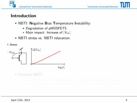
Introduction
NBTI: Negative Bias Temperature Instability:
Degradation of pMOSFETSMain impact: Increase of |Vth|
NBTI stress vs. NBTI relaxation:
1. Stress:
Dynamic NBTI:
Sequence of stress/recovery phase causes fast changing ∆Vth(t)∆Vth(t) potential error source in high-precision analog circuits
April 12th, 2013 5
Lehrstuhl für Technische Elektronik Technische Universität München
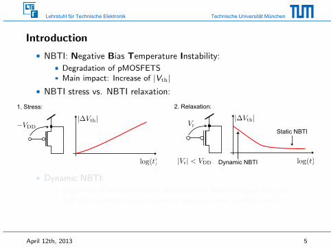
Introduction
NBTI: Negative Bias Temperature Instability:
Degradation of pMOSFETSMain impact: Increase of |Vth|
NBTI stress vs. NBTI relaxation:
1. Stress: 2. Relaxation:
Static NBTI
Dynamic NBTI
Dynamic NBTI:
Sequence of stress/recovery phase causes fast changing ∆Vth(t)∆Vth(t) potential error source in high-precision analog circuits
April 12th, 2013 5
Lehrstuhl für Technische Elektronik Technische Universität München
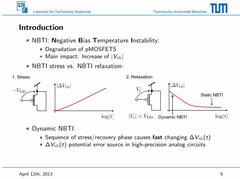
Introduction
NBTI: Negative Bias Temperature Instability:
Degradation of pMOSFETSMain impact: Increase of |Vth|
NBTI stress vs. NBTI relaxation:
1. Stress: 2. Relaxation:
Static NBTI
Dynamic NBTI
Dynamic NBTI:
Sequence of stress/recovery phase causes fast changing ∆Vth(t)∆Vth(t) potential error source in high-precision analog circuits
April 12th, 2013 5
Lehrstuhl für Technische Elektronik Technische Universität München
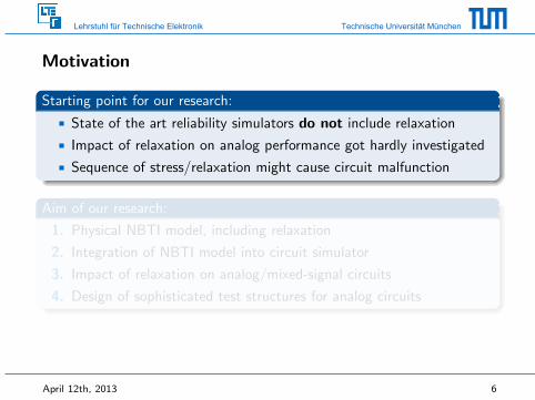
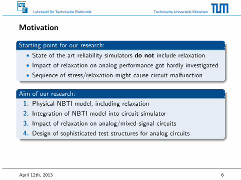
Motivation
Starting point for our research:
State of the art reliability simulators do not include relaxation
Impact of relaxation on analog performance got hardly investigated
Sequence of stress/relaxation might cause circuit malfunction
Aim of our research:
1. Physical NBTI model, including relaxation
2. Integration of NBTI model into circuit simulator
3. Impact of relaxation on analog/mixed-signal circuits
4. Design of sophisticated test structures for analog circuits
April 12th, 2013 6
Lehrstuhl für Technische Elektronik Technische Universität München
Content
1 Introduction and Motivation
2 Physical NBTI Model
3 New Simulation Method for NBTI in Analog CMOS Circuits
4 SC Comparator
5 SAR ADC
6 Conclusion and Outlook
7 References
April 12th, 2013 7
Lehrstuhl für Technische Elektronik Technische Universität München
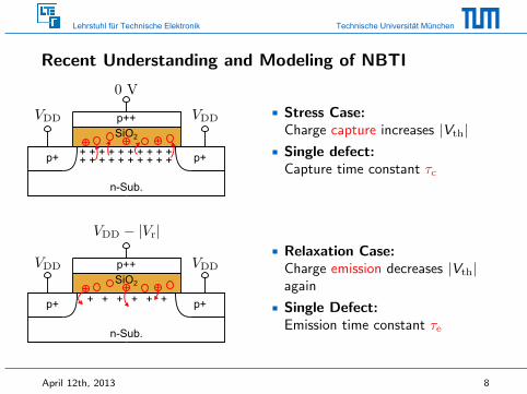
Recent Understanding and Modeling of NBTI
p+
n-Sub.
++
p+
++ + + + + + + + + ++ + + + + + + + + +
p++
SiO2
Stress Case:Charge capture increases |Vth|
Single defect:Capture time constant τc
p+
n-Sub.
++
p+
+
p++
+ +++ + +
SiO2
Relaxation Case:Charge emission decreases |Vth|again
Single Defect:Emission time constant τe
April 12th, 2013 8
Lehrstuhl für Technische Elektronik Technische Universität München
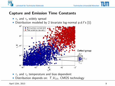
Capture and Emission Time Constants
τc and τe widely spreadDistribution modeled by 2 bivariate log-normal p.d.f’s [1]:
τc and τe temperature and bias dependentDistribution depends on: T ,VGS, CMOS technology
April 12th, 2013 9

Lehrstuhl für Technische Elektronik Technische Universität München
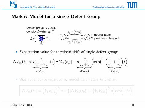
Markov Model for a single Defect Group
1 21: neutral state
2: positively charged
Defect group ( , ),
density within
Expectation value for threshold shift of single defect group:
|∆Vth(t)| ∝ dτe
τe + τc︸ ︷︷ ︸
a(VGS)
+(
|∆Vth(t0)| − dτe
τe + τc︸ ︷︷ ︸
a(VGS)
)
exp(
−( 1
τe+
1
τc︸ ︷︷ ︸
b(VGS)
)
t)
Bias dependence regarded by model parameters k1 and k2:
|∆Vth(t)| =(
k1VGS
)k2
a+(
|∆Vth(t0)| −(
k1VGS
)k2
a)
exp(
−bt)
April 12th, 2013 10

Lehrstuhl für Technische Elektronik Technische Universität München
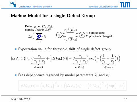
Markov Model for a single Defect Group
1 21: neutral state
2: positively charged
Defect group ( , ),
density within
Expectation value for threshold shift of single defect group:
|∆Vth(t)| ∝ dτe
τe + τc︸ ︷︷ ︸
a(VGS)
+(
|∆Vth(t0)| − dτe
τe + τc︸ ︷︷ ︸
a(VGS)
)
exp(
−( 1
τe+
1
τc︸ ︷︷ ︸
b(VGS)
)
t)
Bias dependence regarded by model parameters k1 and k2:
|∆Vth(t)| =(
k1VGS
)k2
a+(
|∆Vth(t0)| −(
k1VGS
)k2
a)
exp(
−bt)
April 12th, 2013 10
Lehrstuhl für Technische Elektronik Technische Universität München
Markov Model for a single Defect Group
1 21: neutral state
2: positively charged
Defect group ( , ),
density within
Expectation value for threshold shift of single defect group:
|∆Vth(t)| ∝ dτe
τe + τc︸ ︷︷ ︸
a(VGS)
+(
|∆Vth(t0)| − dτe
τe + τc︸ ︷︷ ︸
a(VGS)
)
exp(
−( 1
τe+
1
τc︸ ︷︷ ︸
b(VGS)
)
t)
Bias dependence regarded by model parameters k1 and k2:
|∆Vth(t)| =(
k1VGS
)k2
a+(
|∆Vth(t0)| −(
k1VGS
)k2
a)
exp(
−bt)
April 12th, 2013 10
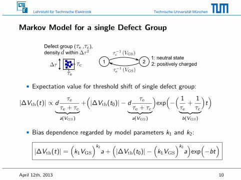
Lehrstuhl für Technische Elektronik Technische Universität München
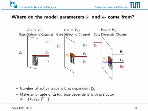
Where do the model parameters k1 and k2 come from?
EF
Gate
EC
ChannelDielectric
VGS ≈ Vth
Channel ChannelGate GateDielectric Dielectric
VGS = Vs,1 VGS = Vs,2
EC
EC
EV
EV
EF
EF
EF
EF
EF
EV
N1N1
∆N
Number of active traps is bias dependent [2]
Make amplitude of ∆Vth bias dependent with prefactorA = (k1VGS)
k2 [1]
April 12th, 2013 11
Lehrstuhl für Technische Elektronik Technische Universität München
Content
1 Introduction and Motivation
2 Physical NBTI Model
3 New Simulation Method for NBTI in Analog CMOS Circuits
4 SC Comparator
5 SAR ADC
6 Conclusion and Outlook
7 References
April 12th, 2013 12
Lehrstuhl für Technische Elektronik Technische Universität München
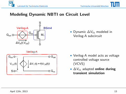
Modeling Dynamic NBTI on Circuit Level
S
M1
ΔVth(t,VGS)
GextGint
Verilog-A BSim4
Dynamic ∆Vth modeled inVerilog-A subcircuit
Gext
S
Gext
Gint
Verilog-A model acts as voltagecontrolled voltage source(VCVS)
∆Vth adapted online duringtransient simulation
April 12th, 2013 13
Lehrstuhl für Technische Elektronik Technische Universität München
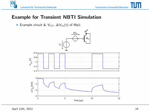
Example for Transient NBTI Simulation
Example circuit & VGS, ∆Vth(t) of Mp1:
Mp1
ΔVth
Vin
−1.4
−1.2
−1
−0.8
−0.6
VG
S [V
]
0 5 10 15−3
−2
−1
0
Time [µs]
∆ V
th [m
V]
April 12th, 2013 14
Lehrstuhl für Technische Elektronik Technische Universität München
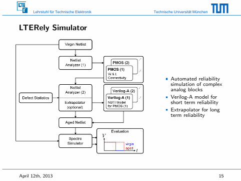
LTERely Simulator
Netlist
Analyzer (1)
Virgin Netlist
Aged Netlist
Verilog-A (1)
NBTI Modelfor PMOS (1)
Automated reliabilitysimulation of complexanalog blocks
Verilog-A model forshort term reliability
Extrapolator for longterm reliability
April 12th, 2013 15
Lehrstuhl für Technische Elektronik Technische Universität München
Content
1 Introduction and Motivation
2 Physical NBTI Model
3 New Simulation Method for NBTI in Analog CMOS Circuits
4 SC Comparator
5 SAR ADC
6 Conclusion and Outlook
7 References
April 12th, 2013 16

Lehrstuhl für Technische Elektronik Technische Universität München
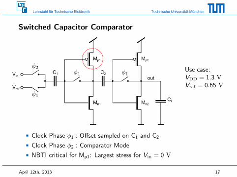
Switched Capacitor Comparator
Mp1
Mn1
Mp2
Mn2
C1 C2
CL
outVin
Vref
Use case:VDD = 1.3 V
Vref = 0.65 V
Clock Phase φ1 : Offset sampled on C1 and C2
Clock Phase φ2 : Comparator Mode
April 12th, 2013 17
Lehrstuhl für Technische Elektronik Technische Universität München
Switched Capacitor Comparator
Use case:VDD = 1.3 V
Vref = 0.65 V
Clock Phase φ1 : Offset sampled on C1 and C2
Clock Phase φ2 : Comparator Mode
NBTI critical for Mp1: Largest stress for Vin = 0 V
April 12th, 2013 17
Lehrstuhl für Technische Elektronik Technische Universität München
SC Comparator: Test Case
Verify correct function by input step from Vin = 0 V to Vref + 20 µV:
0
0.65
1.3
φ 1 [V]
0
0.65
1.3
φ 2 [V]
0
0.65
1.3
Vin
[V] V
in = V
ref + 20µV
0 1 2 3 4 5 6 7 8 9 100
0.65
1.3
Vou
t [V]
Time [µs]
April 12th, 2013 18
Lehrstuhl für Technische Elektronik Technische Universität München
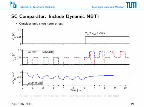
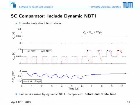
SC Comparator: Include Dynamic NBTI
Consider only short term stress:
0
0.65
1.3
Vin
[V] V
in = V
ref + 20µV
0
0.65
1.3
Vou
t [V]
no NBTI with NBTI
0 1 2 3 4 5 6 7 8 9 10
−1
−0.5
0
Time [µs]
∆ V
th [m
V]
∆ Vth of Mp1
Failure is caused by dynamic NBTI component, before end of life time
April 12th, 2013 19
Lehrstuhl für Technische Elektronik Technische Universität München
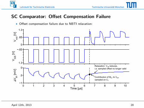
SC Comparator: Offset Compensation Failure
Offset compensation failure due to NBTI relaxation:
0
.65
1.3
Vout[V
]
�1.3
�.65
VG
S[V
]
0 1 2 3 4 5 6 7 8 9 10�1
�.5
0
Vth
[mV
]
Time [µs]
Contribution of Mp1 to Voff,
sampled on C1
Relaxation: Voff reduces,
i.e. sampled offset no longer valid
April 12th, 2013 20
Lehrstuhl für Technische Elektronik Technische Universität München
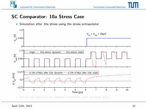
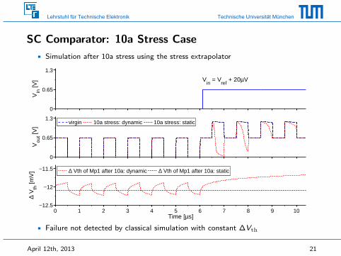
SC Comparator: 10a Stress Case
Simulation after 10a stress using the stress extrapolator
0
0.65
1.3
Vin
[V] V
in = V
ref + 20µV
0
0.65
1.3
Vou
t [V]
virgin 10a stress: dynamic 10a stress: static
0 1 2 3 4 5 6 7 8 9 10−12.5
−12
−11.5
Time [µs]
∆ V
th [m
V]
∆ Vth of Mp1 after 10a: dynamic ∆ Vth of Mp1 after 10a: static
Failure not detected by classical simulation with constant ∆Vth
April 12th, 2013 21
Lehrstuhl für Technische Elektronik Technische Universität München
Content
1 Introduction and Motivation
2 Physical NBTI Model
3 New Simulation Method for NBTI in Analog CMOS Circuits
4 SC Comparator
5 SAR ADC
6 Conclusion and Outlook
7 References
April 12th, 2013 22
Lehrstuhl für Technische Elektronik Technische Universität München
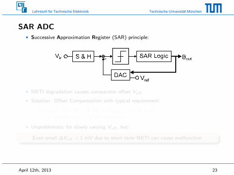
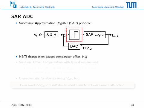
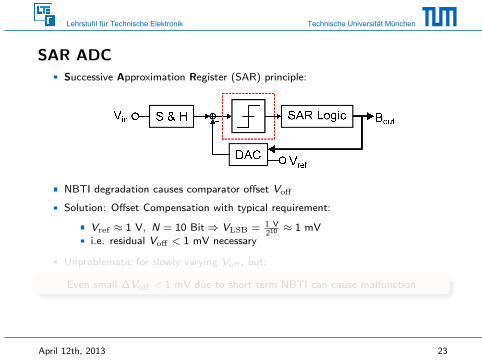
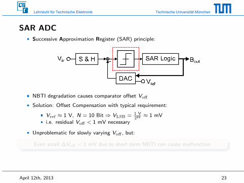
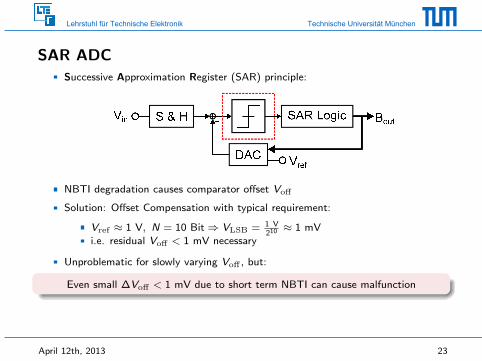
SAR ADC
Successive Approximation Register (SAR) principle:
S & H
NBTI degradation causes comparator offset Voff
Solution: Offset Compensation with typical requirement:
Vref ≈ 1 V, N = 10 Bit ⇒ VLSB = 1 V210
≈ 1 mV
i.e. residual Voff < 1 mV necessary
Unproblematic for slowly varying Voff , but:
Even small ∆Voff < 1 mV due to short term NBTI can cause malfunction
April 12th, 2013 23
Lehrstuhl für Technische Elektronik Technische Universität München
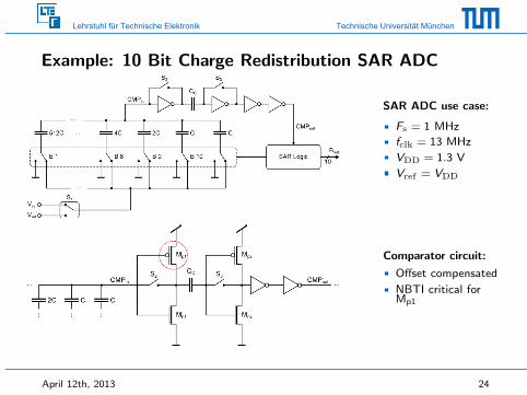
Example: 10 Bit Charge Redistribution SAR ADC
Vin
Vref
SAR ADC use case:
Fs = 1 MHz
fclk = 13 MHz
VDD = 1.3 V
Vref = VDD
Mp1
Mn1
Mp2
Mn2
CC�2 �3
CC2C
...
...
...
...CMPin CMPout ...
Comparator circuit:
Offset compensated
NBTI critical forMp1
April 12th, 2013 24
Lehrstuhl für Technische Elektronik Technische Universität München
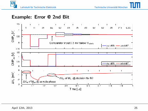
Example: Error @ 2nd Bit
April 12th, 2013 25
Lehrstuhl für Technische Elektronik Technische Universität München
SAR ADC: Errors due to short term NBTIWrong output codes can occur for large variety of input levels
Code deviations of more than |1 LSB| were not found
Observed error rates depend on:
Input signal waveformClock frequency...
Example for full scale sine wave input @ Fs = 1 MHz:
April 12th, 2013 26
Lehrstuhl für Technische Elektronik Technische Universität München
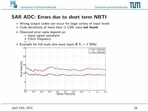
SAR ADC: Errors due to short term NBTIWrong output codes can occur for large variety of input levelsCode deviations of more than |1 LSB| were not found
Observed error rates depend on:Input signal waveformClock frequency...
Example for full scale sine wave input @ Fs = 1 MHz:
0.2 0.3 0.4 0.5 0.6 0.7 0.8 0.9 1 1.1 1.20
5
10
15
20
25
Stress Time [ms]
Err
or R
ate
[%]
fin = 100 kHzfin = 400 kHz
April 12th, 2013 26
Lehrstuhl für Technische Elektronik Technische Universität München
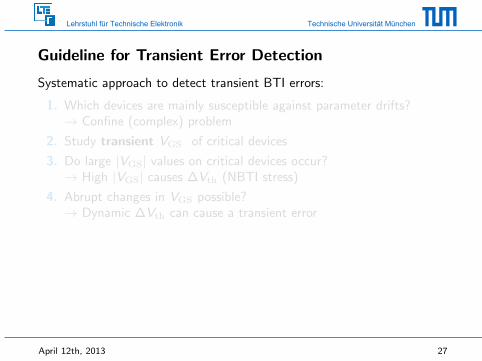
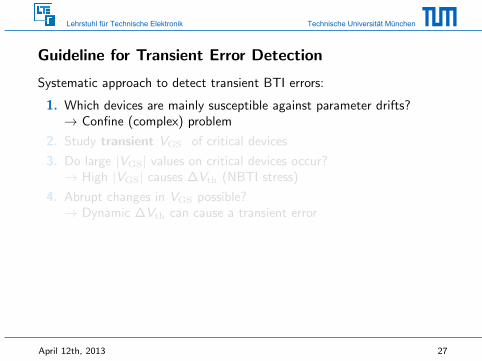
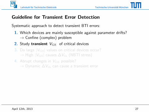
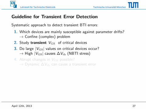
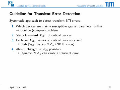
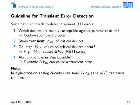
Guideline for Transient Error Detection
Systematic approach to detect transient BTI errors:
1. Which devices are mainly susceptible against parameter drifts?→ Confine (complex) problem
2. Study transient VGS of critical devices
3. Do large |VGS| values on critical devices occur?→ High |VGS| causes ∆Vth (NBTI stress)
4. Abrupt changes in VGS possible?→ Dynamic ∆Vth can cause a transient error
April 12th, 2013 27
Lehrstuhl für Technische Elektronik Technische Universität München
Guideline for Transient Error Detection
Systematic approach to detect transient BTI errors:
1. Which devices are mainly susceptible against parameter drifts?→ Confine (complex) problem
2. Study transient VGS of critical devices
3. Do large |VGS| values on critical devices occur?→ High |VGS| causes ∆Vth (NBTI stress)
4. Abrupt changes in VGS possible?→ Dynamic ∆Vth can cause a transient error
Note:In high-precision analog circuits even small ∆Vth (≈ 1 mV) can causetran. error
April 12th, 2013 28
Lehrstuhl für Technische Elektronik Technische Universität München
Content
1 Introduction and Motivation
2 Physical NBTI Model
3 New Simulation Method for NBTI in Analog CMOS Circuits
4 SC Comparator
5 SAR ADC
6 Conclusion and Outlook
7 References
April 12th, 2013 29
Lehrstuhl für Technische Elektronik Technische Universität München
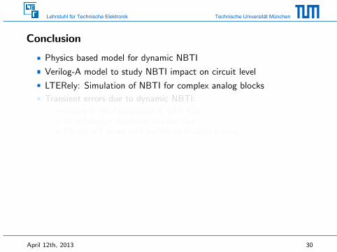
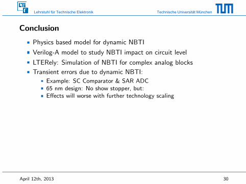
Conclusion
Physics based model for dynamic NBTI
Verilog-A model to study NBTI impact on circuit level
LTERely: Simulation of NBTI for complex analog blocks
Transient errors due to dynamic NBTI:
Example: SC Comparator & SAR ADC65 nm design: No show stopper, but:Effects will worse with further technology scaling
April 12th, 2013 30
Lehrstuhl für Technische Elektronik Technische Universität München
Conclusion
Physics based model for dynamic NBTI
Verilog-A model to study NBTI impact on circuit level
LTERely: Simulation of NBTI for complex analog blocks
Transient errors due to dynamic NBTI:
Example: SC Comparator & SAR ADC65 nm design: No show stopper, but:Effects will worse with further technology scaling
April 12th, 2013 30

Lehrstuhl für Technische Elektronik Technische Universität München
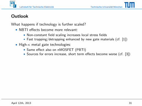
Outlook
What happens if technology is further scaled?
NBTI effects become more relevant:
Non-constant field scaling increases local stress fieldsFast trapping/detrapping enhanced by new gate materials (cf. [1])
High-κ metal gate technologies:
Same effect also on nMOSFET (PBTI)Sources for errors increase, short term effects become worse (cf. [3])
April 12th, 2013 31
Lehrstuhl für Technische Elektronik Technische Universität München
Thank you for your attention
Please feel free to ask questions
April 12th, 2013 32
Lehrstuhl für Technische Elektronik Technische Universität München
Content
1 Introduction and Motivation
2 Physical NBTI Model
3 New Simulation Method for NBTI in Analog CMOS Circuits
4 SC Comparator
5 SAR ADC
6 Conclusion and Outlook
7 References
April 12th, 2013 33
Lehrstuhl für Technische Elektronik Technische Universität München
References I
T. Grasser, P. Wagner, H. Reisinger, T. Aichinger, G. Pobegen,M. Nelhiebel, and B. Kaczer.Analytic modeling of the bias temperature instability usingcapture/emission time maps.In Electron Devices Meeting (IEDM), 2011 IEEE International, pages27.4.1 –27.4.4, dec. 2011.
T. Grasser, B. Kaczer, H. Reisinger, P.-J. Wagner, andM. Toledano-Luque.On the frequency dependence of the bias temperature instability.In Reliability Physics Symposium (IRPS), 2012 IEEE International,pages XT.8.1 –XT.8.7, april 2012.
April 12th, 2013 34
Lehrstuhl für Technische Elektronik Technische Universität München
References II
K. Zhao, J.H. Stathis, B.P. Linder, E. Cartier, and A. Kerber.PBTI under dynamic stress: From a single defect point of view.In Reliability Physics Symposium (IRPS), 2011 IEEE International,pages 4A.3.1 –4A.3.9, april 2011.
M. A. Alam.A Critical Examination of the Mechanics of Dynamic NBTI forPMOSFETs.In Proc. IEDM ’03 Technical Digest Electron Devices Meeting IEEEInt, 2003.
M.A. Alam, H. Kufluoglu, D. Varghese, and S. Mahapatra.A comprehensive model for PMOS NBTI degradation: Recentprogress.Microelectronics Reliability, 47(6):853 – 862, 2007.
April 12th, 2013 35
Lehrstuhl für Technische Elektronik Technische Universität München
References III
M.A. Alam and S. Mahapatra.A comprehensive model of PMOS NBTI degradation.Microelectronics Reliability, 45(1):71 – 81, 2005.
F.R. Chouard, M. Fulde, and D. Schmitt-Landsiedel.Reliability assessment of voltage controlled oscillators in 32nm high-κ metal gate technology.In ESSCIRC, 2010 Proceedings of the, pages 410 –413, sept. 2010.
S. Drapatz, K. Hofmann, G. Georgakos, and D. Schmitt-Landsiedel.Impact of fast-recovering NBTI degradation on stability oflarge-scale SRAM arrays.In Solid-State Device Research Conference (ESSDERC), 2010Proceedings of the European, pages 146 –149, sept. 2010.
April 12th, 2013 36
Lehrstuhl für Technische Elektronik Technische Universität München
References IV
Michael Fulde.Variation Aware Analog and Mixed-Signal Circuit Design inEmerging Multi-Gate CMOS Technologies.Springer Series in Advanced Microelectronics. SpringerScience+Business Media, Dec. 2010.
M. Fulde, D. Schmitt-Landsiedel, and G. Knoblinger.Transient Variations in Emerging SOI Technologies: Modeling andImpact on Analog/Mixed-Signal Circuits.In Circuits and Systems, 2007. ISCAS 2007. IEEE InternationalSymposium on, pages 1249 –1252, may 2007.
W. Goes, F. Schanovsky, T. Grasser, H. Reisinger, and B. Kaczer.Advanced Modeling of Oxide Defects for Random Telegraph Noise.In Noise and Fluctuations (ICNF), 2011 21st InternationalConference on, pages 204 –207, june 2011.
April 12th, 2013 37
Lehrstuhl für Technische Elektronik Technische Universität München
References V
Tibor Grasser.Stochastic charge trapping in oxides: From random telegraph noiseto bias temperature instabilities.Microelectronics Reliability, 52(1):39 – 70, 2012.
T. Grasser, T. Aichinger, G. Pobegen, H. Reisinger, P. Wagner,J. Franco, M. Nelhiebel, and B. Kaczer.The ’permanent’ component of nbti: Composition and annealing.In Reliability Physics Symposium (IRPS), 2011 IEEE International,pages 6A.2.1 –6A.2.9, april 2011.
T. Grasser, T. Aichinger, H. Reisinger, J. Franco, P.-J. Wagner,M. Nelhiebel, C. Ortolland, and B. Kaczer.On the ’permanent’ component of nbti.In Integrated Reliability Workshop Final Report (IRW), 2010 IEEEInternational, pages 2 –7, oct. 2010.
April 12th, 2013 38
Lehrstuhl für Technische Elektronik Technische Universität München
References VI
T. Grasser and B. Kaczer.Evidence that two tightly coupled mechanisms are responsible fornegative bias temperature instability in oxynitride mosfets.Electron Devices, IEEE Transactions on, 56(5):1056 –1062, may2009.
T. Grasser, B. Kaczer, W. Goes, T. Aichinger, P. Hehenberger, andM. Nelhiebel.A two-stage model for negative bias temperature instability.In Reliability Physics Symposium, 2009 IEEE International, pages 33–44, april 2009.
April 12th, 2013 39
Lehrstuhl für Technische Elektronik Technische Universität München
References VII
T. Grasser, B. Kaczer, W. Goes, H. Reisinger, T. Aichinger,P. Hehenberger, P. Wagner, F. Schanovsky, J. Franco, M.T. Luque,and M. Nelhiebel.The paradigm shift in understanding the bias temperature instability:From reaction-diffusion to switching oxide traps.Electron Devices, IEEE Transactions on, 58(11):3652 –3666, nov.2011.
T. Grasser, B. Kaczer, H. Reisinger, P.-J. Wagner, andM. Toledano-Luque.Recent developments in understanding the bias temperatureinstability.In Microelectronics (MIEL), 2012 28th International Conference on,pages 315 –322, may 2012.
April 12th, 2013 40
Lehrstuhl für Technische Elektronik Technische Universität München
References VIII
T. Grasser, H. Reisinger, P. Wagner, F. Schanovsky, W. Goes, andB. Kaczer.The time dependent defect spectroscopy (tdds) for thecharacterization of the bias temperature instability.In Reliability Physics Symposium (IRPS), 2010 IEEE International,pages 16 –25, may 2010.
V. Huard, M. Denais, and C. Parthasarathy.NBTI degradation: From physical mechanisms to modelling.Microelectronics Reliability, 46(1):1 – 23, 2006.
April 12th, 2013 41
Lehrstuhl für Technische Elektronik Technische Universität München
References IX
V. Huard, C. Parthasarathy, N. Rallet, C. Guerin, M. Mammase,D. Barge, and C. Ouvrard.New characterization and modeling approach for NBTI degradationfrom transistor to product level.In Electron Devices Meeting, 2007. IEDM 2007. IEEE International,pages 797 –800, dec. 2007.
Cadence Design Systems Inc.RELIABILITY SIMULATION IN INTEGRATED CIRCUIT DESIGN.Available onlinehttp://w2.cadence.com/whitepapers/5082 ReliabilitySim FNL WP.pdf.
Kjell O. Jeppson and Christer M. Svensson.Negative bias stress of MOS devices at high electric fields anddegradation of MNOS devices.Journal of Applied Physics, 48(5):2004–2014, 1977.
April 12th, 2013 42
Lehrstuhl für Technische Elektronik Technische Universität München
References X
B. Kaczer, T. Grasser, P.J. Roussel, J. Franco, R. Degraeve,L. Ragnarsson, E. Simoen, G. Groeseneken, and H. Reisinger.Origin of nbti variability in deeply scaled pfets.In Reliability Physics Symposium (IRPS), 2010 IEEE International,pages 26 –32, may 2010.
B. Kaczer, S. Mahato, V.V. de Almeida Camargo,M. Toledano-Luque, P.J. Roussel, T. Grasser, F. Catthoor,P. Dobrovolny, P. Zuber, G. Wirth, and G. Groeseneken.Atomistic approach to variability of bias-temperature instability incircuit simulations.In Reliability Physics Symposium (IRPS), 2011 IEEE International,pages XT.3.1 –XT.3.5, april 2011.
April 12th, 2013 43
Lehrstuhl für Technische Elektronik Technische Universität München
References XI
B. Kaczer, P.J. Roussel, T. Grasser, and G. Groeseneken.Statistics of multiple trapped charges in the gate oxide of deeplyscaled mosfet devices - application to nbti.Electron Device Letters, IEEE, 31(5):411 –413, may 2010.
J. Keane, Xiaofei Wang, D. Persaud, and C.H. Kim.An all-in-one silicon odometer for separately monitoring hci, bti, andtddb.Solid-State Circuits, IEEE Journal of, 45(4):817 –829, april 2010.
Tae-Hyoung Kim, R. Persaud, and C.H. Kim.Silicon odometer: An on-chip reliability monitor for measuringfrequency degradation of digital circuits.Solid-State Circuits, IEEE Journal of, 43(4):874 –880, april 2008.
April 12th, 2013 44
Lehrstuhl für Technische Elektronik Technische Universität München
References XII
T.H. Lee and A. Hajimiri.Oscillator phase noise: a tutorial.Solid-State Circuits, IEEE Journal of, 35(3):326 –336, march 2000.
Zhihong Liu, B.W. McGaughy, and J.Z. Ma.Design tools for reliability analysis.In Design Automation Conference, 2006 43rd ACM/IEEE, pages 182–187, 0-0 2006.
Franco Maloberti.Analog Design for CMOS VLSI Systems.Kluwer Academic Publishers, 2001.
April 12th, 2013 45
Lehrstuhl für Technische Elektronik Technische Universität München
References XIII
E. Maricau, Leqi Zhang, J. Franco, P. Roussel, G. Groeseneken, andG. Gielen.A compact nbti model for accurate analog integrated circuitreliability simulation.In Solid-State Device Research Conference (ESSDERC), 2011Proceedings of the European, pages 147 –150, sept. 2011.
J. Martin-Martinez, R. Rodriguez, M. Nafria, and X. Aymerich.Time-dependent variability related to bti effects in mosfets: Impacton cmos differential amplifiers.Device and Materials Reliability, IEEE Transactions on, 9(2):305–310, june 2009.
April 12th, 2013 46
Lehrstuhl für Technische Elektronik Technische Universität München
References XIV
H. Miki, M. Yamaoka, N. Tega, Z. Ren, M. Kobayashi, C.P. D’Emic,Y. Zhu, D.J. Frank, M.A. Guillorn, D. Park, W. Haensch, andK. Torii.Understanding short-term bti behavior through comprehensiveobservation of gate-voltage dependence of rtn in highly scaled high-k / metal-gate pfets.In VLSI Technology (VLSIT), 2011 Symposium on, pages 148 –149,june 2011.
S. More, M. Fulde, F. Chouard, and D. Schmitt-Landsiedel.Reliability analysis of buffer stage in mixed signal application.Advances in Radio Science, 9:225–230, 2011.
April 12th, 2013 47
Lehrstuhl für Technische Elektronik Technische Universität München
References XV
S. More, M. Fulde, F. Chouard, and D. Schmitt-Landsiedel.Reducing Impact of Degradation on Analog Circuits by ChopperStabilization and Autozeroing.In Proc. 12th Int Quality Electronic Design (ISQED) Symp, pages1–6, 2011.
L. Negre, D. Roy, F. Cacho, P. Scheer, S. Jan, S. Boret, D. Gloria,and G. Ghibaudo.Reliability characterization and modeling solution to predict aging of40-nm mosfet dc and rf performances induced by rf stresses.Solid-State Circuits, IEEE Journal of, 47(5):1075 –1083, may 2012.
April 12th, 2013 48
Lehrstuhl für Technische Elektronik Technische Universität München
References XVI
H. Reisinger, O. Blank, W. Heinrigs, A. Muhlhoff, W. Gustin, andSchlunder C.Analysis of NBTI Degradation- and Recovery-Behavior Based onUltra Fast VT-Measurements.In Reliability Physics Symposium Proceedings, 2006. 44th Annual.,IEEE International, pages 448 –453, march 2006.
H. Reisinger, O. Blank, W. Heinrigs, A. Muhlhoff, W. Gustin, andC. Schlunder.Analysis of nbti degradation- and recovery-behavior based on ultrafast vt-measurements.In Reliability Physics Symposium Proceedings, 2006. 44th Annual.,IEEE International, pages 448 –453, march 2006.
April 12th, 2013 49
Lehrstuhl für Technische Elektronik Technische Universität München
References XVII
H. Reisinger, T. Grasser, K. Ermisch, H. Nielen, W. Gustin, andSchlunder C.Understanding and modeling AC BTI.In Reliability Physics Symposium (IRPS), 2011 IEEE International,pages 6A.1.1 –6A.1.8, april 2011.
H. Reisinger, T. Grasser, W. Gustin, and C. Schlunder.The statistical analysis of individual defects constituting NBTI andits implications for modeling DC- and AC-stress.In Reliability Physics Symposium (IRPS), 2010 IEEE International,pages 7 –15, may 2010.
April 12th, 2013 50
Lehrstuhl für Technische Elektronik Technische Universität München
References XVIII
M. Toledano-Luque, B. Kaczer, J. Franco, P.J. Roussel, T. Grasser,T.Y. Hoffmann, and G. Groeseneken.From mean values to distributions of BTI lifetime of deeply scaledFETs through atomistic understanding of the degradation.In VLSI Technology (VLSIT), 2011 Symposium on, pages 152 –153,june 2011.
Christoph Werner, Florian R. Chouard, Stefan Drapatz, and DorisSchmitt-Landsiedel.A statistical MOSFET Aging Model for Monte Carlo Simulationswith HSpice.In Synopsys User Group (SNUG), 2012 Germany, 2012.
April 12th, 2013 51
Lehrstuhl für Technische Elektronik Technische Universität München
References XIX
G.I. Wirth, R. da Silva, and B. Kaczer.Statistical Model for MOSFET Bias Temperature InstabilityComponent Due to Charge Trapping.Electron Devices, IEEE Transactions on, 58(8):2743 –2751, aug.2011.
April 12th, 2013 52


![Produkt Teil 1 [Kompatibilitätsmodus] · Marketinginstrumente II Technische Universität Chemnitz Lehrstuhl Marketing und Handelsbetriebslehre Univ.-Prof. Dr. Cornelia Zanger Wintersemester](https://img.pdfslide.us/doc/110x75/5d0ce4ff88c9931d148b6652/produkt-teil-1-kompatibilitaetsmodus-marketinginstrumente-ii-technische-universitaet.jpg)