Embed Size (px)
Citation preview
Modeling and optimization of photoniccrystal devices based on transformation
optics method
Yinghui Cao,1,2,3 Jun Xie,1 Yongmin Liu,4,5 and Zhenyu Liu1,∗1State Key Laboratory of Applied Optics, Changchun Institute of Optics, Fine Mechanics and
Physics, 3888 East Nanhu Road, Changchun, Jilin 130033, P. R. China2College of Computer Science and Technology, Jilin University, 2699 Qianjin Street,
Changchun, Jilin 130021, P. R. China3 [email protected]
4Department of Mechanical and Industrial Engineering, Department of Electrical andComputer Engineering, Northeastern University, 360 Huntington Avenue, Boston, MA 02115
5 [email protected]∗[email protected]
Abstract: In this paper, we propose a method for designing Pho-tonic Crystal (PhC) devices that consist of dielectric rods with varyingsize. In the proposed design method, PhC devices are modeled with theTransformation Optics (TO) approach, and then they are optimized usingthe gradient method. By applying the TO technique, the original devicemodel is transformed into an equivalent model that consists of uniformand fixed-sized rods, with parameterized permittivity and permeabilitydistributions. Therefore, mesh refinement around small rods can be avoided,and PhC devices can be simulated more efficiently. In addition, gradientof the optimization object function is calculated with the Adjoint-VariableMethod (AVM), which is very efficient for optimizing devices subject tomultiple design variables. The proposed method opens up a new avenue todesign and optimize a variety of photonic devices for optical computing andinformation processing.
© 2014 Optical Society of America
OCIS codes: (130.3120) Integrated optics devices; (130.5296) Photonic crystal waveguides;(350.4238) Nanophotonics and photonic crystals.
References and links1. J. D. Joannopoulos, S. G. Johnson, J. N. Winn, and R. D. Meade, Photonic Crystals: Molding the Flow of Light,
2nd Ed. (Princeton University, 2008).2. I. A. Sukhoivanov, and I. V. Guryev, Photonic Crystals: Physics and Practical Modeling (Springer-Verlag, Berlin,
2009).3. A. Adibi, Y. Xu, R. K. Lee, A. Yariv, and A. Scherer. “Guiding mechanisms in dielectric-core photonic-crystal
optical waveguides,” Phys. Rev. B 64, 033308 (2001).4. P. Bienstman, S. Assefa, S. G. Johnson, J. D. Joannopoulos, G. S. Petrich, and L. A. Kolodziejski, “Taper struc-
tures for coupling into photonic crystal slab waveguides,” J. Opt. Soc. Am. B 20, 1817–1821 (2003).5. K. Dossou, L. C. Botten, C. M. Sterke, R. C. McPhedran, A. A. Asatryan, S. Chen, and J. Brnovic, “Efficient
couplers for photonic crystal waveguides,” Opt. Commun. 265, 207–219 (2006).6. A. Mekis and J. D. Joannopoulos, “Tapered couplers for efficient interfacing between dielectric and photonic
crystal waveguides,” J. Lightw. Technol., 19(6), 861–865 (2001).7. O. Ozgun, M. Kuzuoglu, “Software metamaterials: Transformation media based multiscale techniques for com-
putational electromagnetics”, J. Comput. Phys. 236, 203–219 (2013).
#202078 - $15.00 USD Received 27 Nov 2013; revised 6 Jan 2014; accepted 9 Jan 2014; published 30 Jan 2014(C) 2014 OSA 10 February 2014 | Vol. 22, No. 3 | DOI:10.1364/OE.22.002725 | OPTICS EXPRESS 2725

8. A. J. Ward and J. B. Pendry, “Refraction and geometry in Maxwell’s equation,” J. Mod. Opt. 43(4), 773–793(1996).
9. J. B. Pendry, D. Schurig, and D. R. Smith, “Controlling electromagnetic fields,” Science 312(5781), 1780–1782(2006).
10. Y. M. Liu and X. Zhang, “Recent advances in transformation optics,” Nanoscale 4(17), 5277–5292 (2012).11. L. H. Gabrielli, D. Liu, S. G. Johnson, and M. Lipson, “On-chip transformation optics for multimode waveguide
bends,” Nat. Commun. 3:1217 doi: 10.1038/ncomms2232 (2012).12. Q. Wu, J. P. Turpin, and D. H. Werner, “Integrated photonic systems based on transformation optics enabled
gradient index devices,” Light: Science & Applications (2012) 1, e38; doi:10.1038/lsa.2012.38.13. P. Sanchis, P. Villalba, F. Cuesta, A. Hakansson, A. Griol, J. V. Galan, A. Brimont, and J. Marti, “Highly efficient
crossing structure for silicon-on-insulator waveguides,” Opt. Lett. 34(18), 2760–2762 (2009).14. Y. Zhang, S. Yang, A. E. J. Lim, G. Q. Lo, C. Galland, T. Baehr-Jones, and M. Hochberg, “A compact and low
loss Y-junction for submicron silicon waveguide,” Opt. Express 21(1), 1310–1316 (2013).15. C. M. Lalau-Keraly, S. Bhargava, O. D. Miller, and E. Yablonovitch, “Adjoint shape optimization applied to
electromagnetic design.” Opt. Express 21(18), 21693–21701 (2013).16. N. K. Georgieva, S. Glavic, M. H. Bakr, and J. W. Bandler, “Feasible Adjoint Sensitivity Technique for EM
Design Optimization,” IEEE Tans. Microwave Theory Tech. 50(12), 2751–2758 (2002).17. G. Veronis, R. W. Dutton, and S. Fan, “Method for sensitivity analysis of photonic crystal devices,” Opt. Lett.
29(19), 2288–2290 (2004).18. J. S. Jensen and O. Sigmund, “Topology optimization of photonic crystal structures: a high-bandwidth low-loss
T-junction waveguide,” J. Opt. Soc. Am. B 22(6), 1191–1198 (2005).19. COMSOL Multiphysics, http://www.comsol.com/20. D. Marcuse, Theory of Dielectric Optical Waveguides (Academic Press, 1974).21. S. G. Johnson and J. D. Joanopoulos, “Block-iterative frequency-domain methods for Maxwell’s equation in a
planewave basis,” Opt. Express 8(3), 173–190 (2001).22. M. Schmidt, http://www.di.ens.fr/˜Emschmidt/Software/minConf.html23. M. Minkov and V. Savona, “Effect of hole-shape irregularities on photonic crystal waveguides,” Opt. Lett. 37(15),
3108–3110 (2012).24. V. Savona, “Electromagnetic modes of a disordered photonic crystal,” Phys. Rev. B 83, 085301 (2011).
1. Introduction
Photonic Crystals (PhCs) are novel artificial materials that allow us to manipulate electromag-netic waves in an unprecedented manner [1,2]. A fundamental property of PhCs is the PhotonicBand Gap (PBG) [1, 2], which prohibits light propagation in PhCs at certain frequency rangesand can be exploited to control light propagation. By introducing defects in PhCs, we can re-alize novel photonic components and devices, such as PhC waveguides, filters, demultiplexers,etc [1, 2]. An important condition for the application of PhC waveguides is the efficient lightcoupling between PhC waveguides and other conventional optical waveguides. For some PhCline-defect waveguides that comprise air-holes in a dielectric medium, good light coupling canbe achieved by directly connecting the PhC waveguide with a dielectric slab waveguide [3]. ForPhC line-defect waveguides composed of dielectric rods, couplers with tapered structure, suchas tapered PhC couplers [4, 5] and tapered dielectric waveguides [6] can be used for efficientoptical mode coupling. In this work, we consider the possibility of a PhC coupler that consistsof varying-sized dielectric rods. Comparing with tapered PhC coupler that normally have 7∼10layers of rods [4, 5], the proposed PhC coupler is very compact, consisting of only 3 layers ofdielectric rods along the light propagation direction.
The simulation and optimization of photonic components that contain both electrically largeand small features is very challenging, because refined mesh grids around the small featuresmay significantly increase the computational overhead [7]. As shown in the design examplesof section 3 and 4, PhC devices may contain dielectric rods that are much smaller than others,thus mesh refinements are needed to capture the local variations of the device geometry andelectromagnetic field in conventional simulation and optimization process. This will lead to anincrease of unknowns to be solved, and may cause problems of generating meshes of goodquality around these small rods. The above difficulties, which are referred to as multi-scale
#202078 - $15.00 USD Received 27 Nov 2013; revised 6 Jan 2014; accepted 9 Jan 2014; published 30 Jan 2014(C) 2014 OSA 10 February 2014 | Vol. 22, No. 3 | DOI:10.1364/OE.22.002725 | OPTICS EXPRESS 2726
(b)(a) (c)
ra
rc
(ε1, μ1)
Ω2
Ω1
(ε2, μ2)
y
x
˜Ω2
y
(ε2, μ2)
rbra
˜Ω1
(ε1, μ1)
(d)
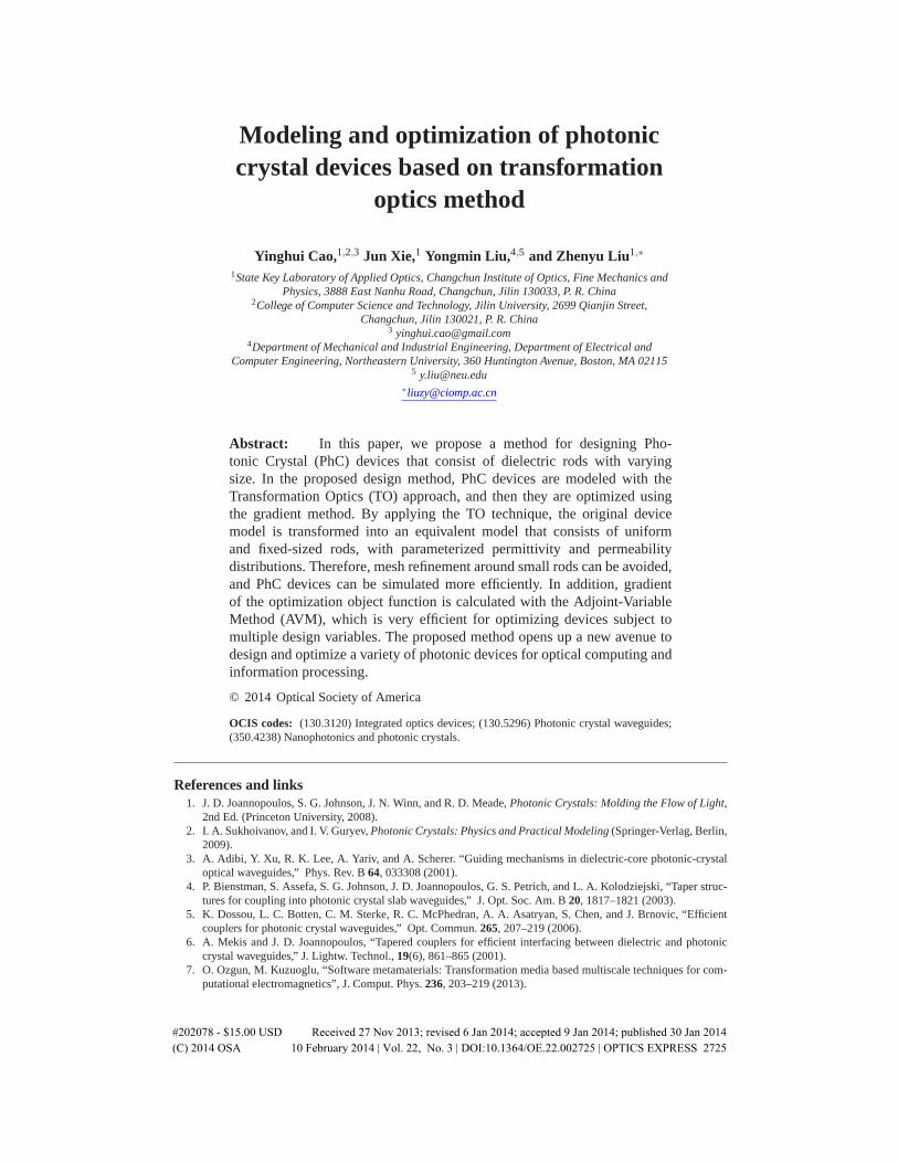
Fig. 1. (a) A PhC device consisting of varying-sized dielectric rods. (b) Transformed modelof (a), in which the transformed rods have a uniform and fixed size. Gray color representsthe permittivity distributions. (c) A single dielectric rod, surrounded by air. (d) Transformedmodel of (c).
problems [7], may become severe when the PhC device contains several dozens to hundreds ofsmall rods. To avoid the multi-scale problems, we can apply the recently developed TO tech-nique [7–12] to transform the original device model into an equivalent model, which consistsof uniform and fixed-sized rods, with parameterized permittivity and permeability distribution.Therefore, mesh refinement around small sized rods can be avoided, and PhC device can besimulated more efficiently.
Photonic devices with varying geometry can be optimized with heuristic methods, such as thegenetic algorithm [13] and the particle swarm algorithm [14]. However, because of their highcomputational cost, heuristic methods are inefficient for devices with lots of design variables[15]. In this work, we use a gradient method to optimize PhC devices, where the gradientof optimization object is calculated with the Adjoint Variable Method (AVM) [16–18]. Byusing the AVM method, for each optimization iteration only one forward problem and oneadjoint problem need to be solved. Therefore, the optimization is very efficient for devices withcomplex structures [15, 16].
2. Transformed model of PhC device
Figure 1(a) shows the structure of a PhC device that consists of dielectric rods with varyingsize. To avoid the multi-scale problems, we use the TO technique [7–11] to transform the orig-inal device model into an equivalent model that consists of rods with a uniform and fixed size,as shown in Fig. 1(b). The transformed rods and surrounding medium have anisotropic permit-tivity and permeability distributions, parameterized by radii of the rods in real geometry. Theparameterized permittivity and permeability distributions can be derived using the TO tech-nique [7–11]. Therefore, optimization of the original device is replaced by optimization of theparameterized permittivity and permeability distribution of the transformed device model.
A single dielectric rod and the transformed model is shown in Figs. 1(c) and 1(d), respec-tively. The dielectric rod in real geometry has a radius of rc, and is stretched to be rb in thetransformed model. The surrounding air of the rod in Fig. 1(c) is transformed into the surround-ing medium layer of the stretched rod in Fig. 1(d), while the outer boundary of the surroundingmedium is kept as same as ra after the transformation. Region of the real dielectric rod andsurrounding air are denoted by Ω1 and Ω2, respectively. In the transformed model, region ofthe stretched rod and the surrounding medium are denoted by ˜Ω1 and ˜Ω2, respectively. Posi-tion vector in the original (transformed) geometry is denoted by r(x,y) (r(x, y)). Therefore, the
#202078 - $15.00 USD Received 27 Nov 2013; revised 6 Jan 2014; accepted 9 Jan 2014; published 30 Jan 2014(C) 2014 OSA 10 February 2014 | Vol. 22, No. 3 | DOI:10.1364/OE.22.002725 | OPTICS EXPRESS 2727
(a) (b) (c)
Fig. 2. (a) Light scattering of a single dielectric rod. (b) Light scattering of the same dielec-tric rod, using the transformed model. (c) The difference of the field distribution between(a) and (b) in the region of r > ra, showing almost negligible difference (in the order of10−4).
coordinate transformation from the original geometry of Fig. 1(c) to the transformed geometryof Fig. 1(d) can be defined as
r =‖ rb ‖‖ rc ‖ r =
rb
rcr
(
r ∈ Ω1, r ∈ ˜Ω1
)
(1)
and
r =‖ ra − rb ‖‖ ra − rc ‖ (r− rc)+ rb =
ra − rb
ra − rc(r− rc)+ rb
(
r ∈ Ω2, r ∈ ˜Ω2
)
(2)
With the above coordinate transformation, the permittivity and permeability distribution of thetransformed model in Fig. 1(d) can be calculated as [7, 11]
εr =1
detJεr, μr =
JTJdetJ
μr (3)
where J is the Jacobian of the coordinate transformation
J =∂ (x, y)∂ (x,y)
=
(
∂ x/∂x ∂ x/∂y∂ y/∂x ∂ y/∂y
)
(4)
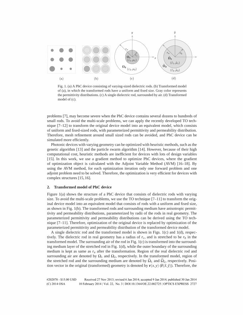
In this work, we use commercial FEM software package COMSOL [19] to simulate PhCdevices, with the transformed device model. To verify the transformed model, we first simulatelight scattering from the original dielectric rod in Fig. 1(c), and then compare it with simulationusing the transformed model in Fig. 1(d). In the simulation we set ra = 0.45µm, rb = 0.3µm,and rc = 0.125µm. Refractive index of the dielectric rod is nrod = 3.4. We assume the incidentlight propagates along x-axis, at the wavelength of λ = 1µm. The incident light polarizes alongz-axis (TM mode), with the electric field intensity of |E| = 1. The total electric field obtainedfrom simulations using the original and transformed model is shown in Figs. 2(a) and 2(b),respectively. Comparing Fig. 2(b) with Fig. 2(a), we can see that the electric field distributioninside the transformed rod is stretched. However, in the region r > ra, the difference of theelectric field between the two simulations is negligible (∼ 10−4), as shown in Fig. 2(c). Thusfor an outside observer, the transformed rod in Fig. 2(b) “looks” identical to the original rod inFig. 2(a).
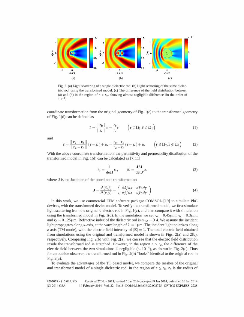
To evaluate the advantages of the TO based model, we compare the meshes of the originaland transformed model of a single dielectric rod, in the region of r ≤ rb. rb is the radius of
#202078 - $15.00 USD Received 27 Nov 2013; revised 6 Jan 2014; accepted 9 Jan 2014; published 30 Jan 2014(C) 2014 OSA 10 February 2014 | Vol. 22, No. 3 | DOI:10.1364/OE.22.002725 | OPTICS EXPRESS 2728
(a) (b) (c) (d) (e)
Fig. 3. (a) Meshes of the transformed rod. (b)–(e) Meshes of the original model, in regionof r ≤ rb. Radius of the rod is rc = 0.2,0.1,0.05,0.01µm, respectively.
the transformed rod, which is set as rb = 0.3µm as above. Meshes in the region of r ≥ rb
can be generated identically for the original and transformed model, so they are ignored in thecomparison. In the region of r ≤ rb, triangular mesh grids are generated, and quadratic elementsare used. Meshes of the transformed rod, which just occupy the region of r ≤ rb, are shown inFig. 3(a). In the region of r ≤ rb, meshes of the original model are shown in Figs. 3(b)–3(e), withrod radius of rc = 0.2,0.1,0.05,0.01µm, respectively. Comparing Fig. 3(a) with Figs. 3(b)–3(e),we can see that in order to accurately capture the small geometrical features, meshes aroundthe rod in original model is much denser than the meshes of the transformed rod, especiallyfor rod with smaller radius. Statistic data of meshes in region of r ≤ rb, including number ofelements, mesh points, and degrees of freedom, are listed in Table 1. Data in Table 1 shows,for meshes of rod with radius of rc = 0.2 ∼ 0.001µm, the number of degrees of freedom isapproximately 2 ∼ 7 times of that of the transformed model. From such a comparison, we canconclude that our TO based approach will be superior over conventional methods, especiallyfor complex geometries with many variable and small features.
Table 1. Statistic data of meshes of the original and transformed model, in the region ofr ≤ rb. Unit for radius: µm.
Transformed Model Original Modelrb = 0.3 rc = 0.2 rc = 0.1 rc = 0.05 rc = 0.01 rc = 0.005 rc = 0.001
number of element 232 484 744 914 1406 1592 1906mesh points 137 263 393 478 724 817 974
degrees of freedom 1010 2018 3058 3738 5706 6450 7706
3. Optimization of PhC coupler
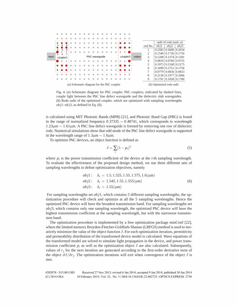
Figure 4(a) is a schematic diagram of the proposed PhC coupler. An input coupler, denotedas coupler1, couples light between the input dielectric slab waveguide and the PhC line de-fect waveguide. Similarly, an output coupler, denoted as coupler2, couples light between thePhC waveguide and the output slab waveguide. The input and output coupler are symmetric,converting the slab waveguide mode into the PhC line defect waveguide mode or vice versa.Both the input and output slab waveguide are single mode waveguides, with core thicknessof d = 1µm, and refractive index of nco = 1.5. The slab waveguide core is surrounded by air.The dispersion relation and guided mode of the slab waveguide can be obtained by solving theeigenvalue equation of the dielectric slab waveguide [20].
We assume the period of bulk PhC is a = 0.6µm. and the radius of the dielectric rod inbulk PhC is r0 = 0.125a, with refractive index of nrod = 3.4. Band structure of the bulk PhC
#202078 - $15.00 USD Received 27 Nov 2013; revised 6 Jan 2014; accepted 9 Jan 2014; published 30 Jan 2014(C) 2014 OSA 10 February 2014 | Vol. 22, No. 3 | DOI:10.1364/OE.22.002725 | OPTICS EXPRESS 2729
1 4 7
2 5 8
3 6 9
coupler1 coupler2PhC waveguideinput output
(a) Schematic diagram for the PhC coupler
radii of rods (unit: a)rod No. ob j1 ob j2 ob j3
1 0.2583 0.2600 0.26342 0.1549 0.1736 0.17503 0.1208 0.1274 0.12814 0.0819 0.0760 0.07555 0.1973 0.2168 0.21756 0.1699 0.1751 0.17567 0.0779 0.0836 0.08338 0.2130 0.1977 0.20669 0.1791 0.1858 0.1780
(b) Optimized rods radii
Fig. 4. (a) Schematic diagram for PhC coupler. PhC couplers, indicated by dashed lines,couple light between the PhC line defect waveguide and the dielectric slab waveguides.(b) Rods radii of the optimised coupler, which are optimized with sampling wavelengthsob j1–ob j3, as defined in Eq. (6).
is calculated using MIT Photonic Bands (MPB) [21], and Photonic Band Gap (PBG) is foundin the range of normalized frequency 0.37335 ∼ 0.48741, which corresponds to wavelength1.23µm ∼ 1.61µm. A PhC line defect waveguide is formed by removing one row of dielectricrods. Numerical simulations show that odd mode of the PhC line defect waveguide is supportedin the wavelength range of 1.3µm ∼ 1.6µm.
To optimize PhC devices, an object function is defined as
J = ∑i(1− pi)
2 (5)
where pi is the power transmission coefficient of the device at the i-th sampling wavelength.To evaluate the effectiveness of the proposed design method, we use three different sets ofsampling wavelengths to define optimization objectives, namely
ob j1 : λi = 1.5,1.525,1.55,1.575,1.6(µm)
ob j2 : λi = 1.545,1.55,1.555(µm) (6)
ob j3 : λi = 1.55(µm)
For sampling wavelengths set ob j1, which contains 5 different sampling wavelengths, the op-timization procedure will check and optimize at all the 5 sampling wavelengths. Hence theoptimized PhC device will have the broadest transmission band. For sampling wavelengths setob j3, which contains only one sampling wavelength, the optimized PhC device will have thehighest transmission coefficient at the sampling wavelength, but with the narrowest transmis-sion band.
The optimization procedure is implemented by a free optimization package minConf [22],where the limited memory Broyden-Fletcher-Goldfarb-Shanno (LBFGS) method is used to iter-atively minimize the value of the object function J. For each optimization iteration, permittivityand permeability distribution of the transformed device model is calculated. Wave equations ofthe transformed model are solved to simulate light propagation in the device, and power trans-mission coefficient pi as well as the optimization object J are also calculated. Subsequently,values of r j for the next iteration are generated according to the first-order derivative term ofthe object ∂J/∂ r j. The optimization iterations will exit when convergence of the object J ismet.
#202078 - $15.00 USD Received 27 Nov 2013; revised 6 Jan 2014; accepted 9 Jan 2014; published 30 Jan 2014(C) 2014 OSA 10 February 2014 | Vol. 22, No. 3 | DOI:10.1364/OE.22.002725 | OPTICS EXPRESS 2730
The first-order derivative of the object function J subject to the design variable r j is calculatedas
∂J∂ r j
= ∑i
2(1− pi)∂ pi
∂ r j(7)
where the design variable r j is the radius of the j-th rod of the PhC device. In the transformeddevice model r j represents a parameter of the permittivity and permeability distribution of thej-th transformed rod and its surrounding medium. The partial derivative term ∂ pi/∂ r j needsto be calculated for each design variable r j, and thus may results in intensive computationalcost during the optimization procedure. In this work, the partial derivative term ∂ pi/∂ r j iscalculated effectively by using the adjoint variable method [15–18], where merely one forwardproblem and one additional adjoint problem need to be solved to obtain the partial derivativeterm ∂ pi/∂ r j for all the design variables. To ensure the symmetry of the optimized PhC devices,the partial derivative term ∂ pi/∂ r j of dielectric rods at symmetric positions are averaged in theoptimization process.
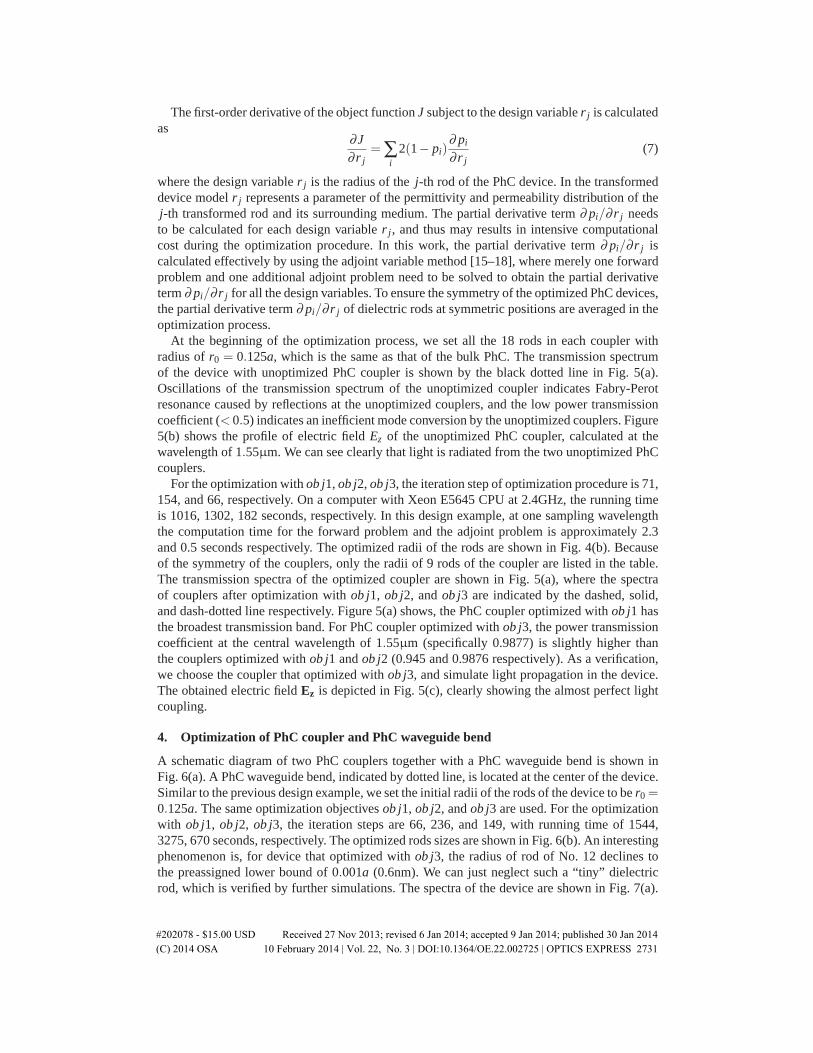
At the beginning of the optimization process, we set all the 18 rods in each coupler withradius of r0 = 0.125a, which is the same as that of the bulk PhC. The transmission spectrumof the device with unoptimized PhC coupler is shown by the black dotted line in Fig. 5(a).Oscillations of the transmission spectrum of the unoptimized coupler indicates Fabry-Perotresonance caused by reflections at the unoptimized couplers, and the low power transmissioncoefficient (< 0.5) indicates an inefficient mode conversion by the unoptimized couplers. Figure5(b) shows the profile of electric field Ez of the unoptimized PhC coupler, calculated at thewavelength of 1.55µm. We can see clearly that light is radiated from the two unoptimized PhCcouplers.
For the optimization with ob j1, ob j2, ob j3, the iteration step of optimization procedure is 71,154, and 66, respectively. On a computer with Xeon E5645 CPU at 2.4GHz, the running timeis 1016, 1302, 182 seconds, respectively. In this design example, at one sampling wavelengththe computation time for the forward problem and the adjoint problem is approximately 2.3and 0.5 seconds respectively. The optimized radii of the rods are shown in Fig. 4(b). Becauseof the symmetry of the couplers, only the radii of 9 rods of the coupler are listed in the table.The transmission spectra of the optimized coupler are shown in Fig. 5(a), where the spectraof couplers after optimization with ob j1, ob j2, and ob j3 are indicated by the dashed, solid,and dash-dotted line respectively. Figure 5(a) shows, the PhC coupler optimized with ob j1 hasthe broadest transmission band. For PhC coupler optimized with ob j3, the power transmissioncoefficient at the central wavelength of 1.55µm (specifically 0.9877) is slightly higher thanthe couplers optimized with ob j1 and ob j2 (0.945 and 0.9876 respectively). As a verification,we choose the coupler that optimized with ob j3, and simulate light propagation in the device.The obtained electric field Ez is depicted in Fig. 5(c), clearly showing the almost perfect lightcoupling.
4. Optimization of PhC coupler and PhC waveguide bend
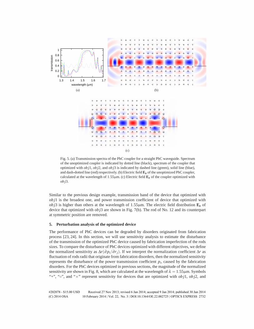
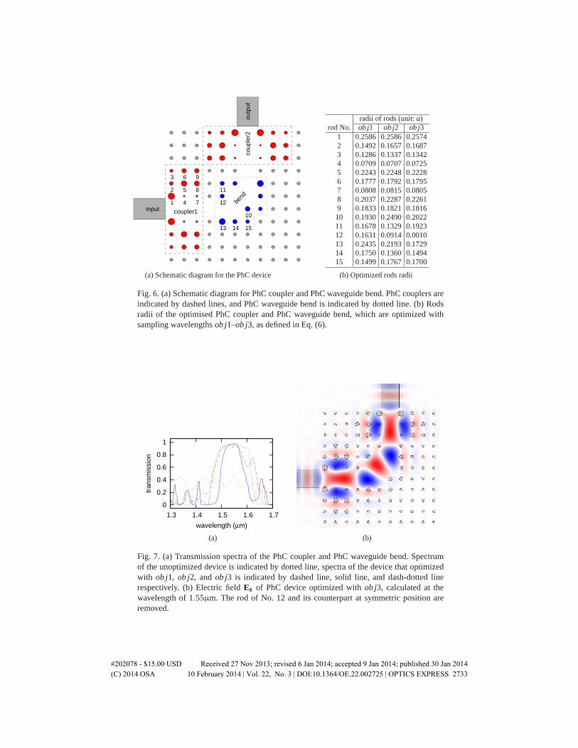
A schematic diagram of two PhC couplers together with a PhC waveguide bend is shown inFig. 6(a). A PhC waveguide bend, indicated by dotted line, is located at the center of the device.Similar to the previous design example, we set the initial radii of the rods of the device to be r0 =0.125a. The same optimization objectives ob j1, ob j2, and ob j3 are used. For the optimizationwith ob j1, ob j2, ob j3, the iteration steps are 66, 236, and 149, with running time of 1544,3275, 670 seconds, respectively. The optimized rods sizes are shown in Fig. 6(b). An interestingphenomenon is, for device that optimized with ob j3, the radius of rod of No. 12 declines tothe preassigned lower bound of 0.001a (0.6nm). We can just neglect such a “tiny” dielectricrod, which is verified by further simulations. The spectra of the device are shown in Fig. 7(a).
#202078 - $15.00 USD Received 27 Nov 2013; revised 6 Jan 2014; accepted 9 Jan 2014; published 30 Jan 2014(C) 2014 OSA 10 February 2014 | Vol. 22, No. 3 | DOI:10.1364/OE.22.002725 | OPTICS EXPRESS 2731
0
0.2
0.4
0.6
0.8
1
1.3 1.4 1.5 1.6 1.7
tran
smis
sion
wavelength (μm)
(a) (b)
(c)
Fig. 5. (a) Transmission spectra of the PhC coupler for a straight PhC waveguide. Spectrumof the unoptimized coupler is indicated by dotted line (black), spectrum of the coupler thatoptimized with ob j1, ob j2, and ob j3 is indicated by dashed line (green), solid line (blue),and dash-dotted line (red) respectively. (b) Electric field Ez of the unoptimized PhC coupler,calculated at the wavelength of 1.55µm. (c) Electric field Ez of the coupler optimized withob j3.
Similar to the previous design example, transmission band of the device that optimized withob j1 is the broadest one, and power transmission coefficient of device that optimized withob j3 is higher than others at the wavelength of 1.55µm. The electric field distribution Ez ofdevice that optimized with ob j3 are shown in Fig. 7(b). The rod of No. 12 and its counterpartat symmetric position are removed.
5. Perturbation analysis of the optimized device
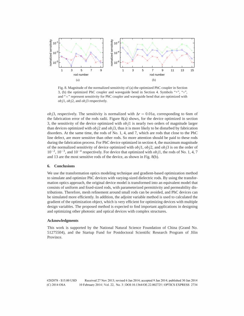
The performance of PhC devices can be degraded by disorders originated from fabricationprocess [23, 24]. In this section, we will use sensitivity analysis to estimate the disturbanceof the transmission of the optimized PhC device caused by fabrication imperfection of the rodssizes. To compare the disturbance of PhC devices optimized with different objectives, we definethe normalized sensitivity as Δr(∂ pi/∂ r j). If we interpret the normalization coefficient Δr asfluctuation of rods radii that originate from fabrication disorders, then the normalized sensitivityrepresents the disturbance of the power transmission coefficient pi, caused by the fabricationdisorders. For the PhC devices optimized in previous sections, the magnitude of the normalizedsensitivity are shown in Fig. 8, which are calculated at the wavelength of λ = 1.55µm. Symbols“+”, “◦”, and “×” represent sensitivity for devices that are optimized with ob j1, ob j2, and
#202078 - $15.00 USD Received 27 Nov 2013; revised 6 Jan 2014; accepted 9 Jan 2014; published 30 Jan 2014(C) 2014 OSA 10 February 2014 | Vol. 22, No. 3 | DOI:10.1364/OE.22.002725 | OPTICS EXPRESS 2732
13 14 15
10
1 4 7 12
2 5 8 11
3 6 9
input
outp
ut
bend
coupler1
coup
ler2
(a) Schematic diagram for the PhC device
radii of rods (unit: a)rod No. ob j1 ob j2 ob j3
1 0.2586 0.2586 0.25742 0.1492 0.1657 0.16873 0.1286 0.1337 0.13424 0.0709 0.0707 0.07255 0.2243 0.2248 0.22286 0.1777 0.1792 0.17957 0.0808 0.0815 0.08058 0.2037 0.2287 0.22619 0.1833 0.1821 0.181610 0.1930 0.2490 0.202211 0.1678 0.1329 0.192312 0.1631 0.0914 0.001013 0.2435 0.2193 0.172914 0.1750 0.1360 0.149415 0.1499 0.1767 0.1700
(b) Optimized rods radii
Fig. 6. (a) Schematic diagram for PhC coupler and PhC waveguide bend. PhC couplers areindicated by dashed lines, and PhC waveguide bend is indicated by dotted line. (b) Rodsradii of the optimised PhC coupler and PhC waveguide bend, which are optimized withsampling wavelengths ob j1–ob j3, as defined in Eq. (6).
0
0.2
0.4
0.6
0.8
1
1.3 1.4 1.5 1.6 1.7
tran
smis
sion
wavelength (μm)
(a) (b)
Fig. 7. (a) Transmission spectra of the PhC coupler and PhC waveguide bend. Spectrumof the unoptimized device is indicated by dotted line, spectra of the device that optimizedwith ob j1, ob j2, and ob j3 is indicated by dashed line, solid line, and dash-dotted linerespectively. (b) Electric field Ez of PhC device optimized with ob j3, calculated at thewavelength of 1.55µm. The rod of No. 12 and its counterpart at symmetric position areremoved.
#202078 - $15.00 USD Received 27 Nov 2013; revised 6 Jan 2014; accepted 9 Jan 2014; published 30 Jan 2014(C) 2014 OSA 10 February 2014 | Vol. 22, No. 3 | DOI:10.1364/OE.22.002725 | OPTICS EXPRESS 2733
10-5
10-3
10-1
1 3 5 7 9
nom
aliz
ed s
ensi
tivity
rod number
(a)
10-6
10-4
10-2
1 3 5 7 9 11 13 15
nom
aliz
ed s
ensi
tivity
rod number
(b)
Fig. 8. Magnitude of the normalized sensitivity of (a) the optimized PhC coupler in Section3, (b) the optimized PhC coupler and waveguide bend in Section 4. Symbols “+”, “◦”,and “×” represent sensitivity for PhC coupler and waveguide bend that are optimized withob j1, ob j2, and ob j3 respectively.
ob j3, respectively. The sensitivity is normalized with Δr = 0.01a, corresponding to 6nm ofthe fabrication error of the rods radii. Figure 8(a) shows, for the device optimized in section3, the sensitivity of the device optimized with ob j1 is nearly two orders of magnitude largerthan devices optimized with ob j2 and ob j3, thus it is more likely to be disturbed by fabricationdisorders. At the same time, the rods of No. 1, 4, and 7, which are rods that close to the PhCline defect, are more sensitive than other rods. So more attention should be paid to these rodsduring the fabrication process. For PhC device optimized in section 4, the maximum magnitudeof the normalized sensitivity of device optimized with ob j1, ob j2, and ob j3 is on the order of10−2, 10−3, and 10−4 respectively. For device that optimized with ob j1, the rods of No. 1, 4, 7and 13 are the most sensitive rods of the device, as shown in Fig. 8(b).
6. Conclusions
We use the transformation optics modeling technique and gradient-based optimization methodto simulate and optimize PhC devices with varying-sized dielectric rods. By using the transfor-mation optics approach, the original device model is transformed into an equivalent model thatconsists of uniform and fixed-sized rods, with parameterized permittivity and permeability dis-tributions. Therefore, mesh refinement around small rods can be avoided, and PhC devices canbe simulated more efficiently. In addition, the adjoint variable method is used to calculated thegradient of the optimization object, which is very efficient for optimizing devices with multipledesign variables. The proposed method is expected to find important applications in designingand optimizing other photonic and optical devices with complex structures.
Acknowledgments
This work is supported by the National Natural Science Foundation of China (Grand No.51275504), and the Startup Fund for Postdoctoral Scientific Research Program of JilinProvince.
#202078 - $15.00 USD Received 27 Nov 2013; revised 6 Jan 2014; accepted 9 Jan 2014; published 30 Jan 2014(C) 2014 OSA 10 February 2014 | Vol. 22, No. 3 | DOI:10.1364/OE.22.002725 | OPTICS EXPRESS 2734