Embed Size (px)
Citation preview

Modeling and Layout Optimization for Robust 3D-IC
Integration with TSVs
David Z. Pan Dept. of Electrical and Computer Engineering
The University of Texas at Austin http://www.cerc.utexas.edu/utda
HSICS, Dallas, 4/30/2013
2
Outline
t Introduction
t Full-chip/package Thermal Mechanical Stress Modeling
t Stress-induced Impact
t Mechanical Reliability
t Mobility/Timing Variations
t Stress-aware Electromigration
t Conclusion

3
Thermal/Mechanical Stress
CTE : Coefficient of thermal expansion
TSV: 250 °C ~400 °C process (Higher than operating temperature) Since Cu has larger CTE than Si, tensile stress is in Si near TSV.
Silicon Cu TSV
< Tensile stress >
FEA simulation structure of a single TSV # variables: 400K, Memory: 2GB runtime: 40min

Stress => Variability/Reliability t Systematic Variations
› Mobility › Timing
t Reliability (interfacial crack, EM, etc.)
Si Cu
Electromigration Effect – Open
Electromigration Effect – Short Interfacial Crack

Stress Tensor
⎥⎥⎥
⎦
⎤
⎢⎢⎢
⎣
⎡
==
zzzyzx
yzyyyx
xzxyxx
ij
σσσ
σσσ
σσσ
σσ
i: stress acts on a plane normal to the i-axis j: direction in which the stress acts
normal stress shear stress
TSV
Pre-compute stress tensors around TSV along radial line, using detailed FEA simulations
θ⎥⎥⎥
⎦
⎤
⎢⎢⎢
⎣
⎡
−
⎥⎥⎥
⎦
⎤
⎢⎢⎢
⎣
⎡
⎥⎥⎥
⎦
⎤
⎢⎢⎢
⎣
⎡ −
=
1000cossin0sincos
1000cossin0sincos
θθ
θθ
σσσ
σσσ
σσσ
θθ
θθ
θ
θθθθ
θ
zzzzr
zr
rzrrr
xyzS
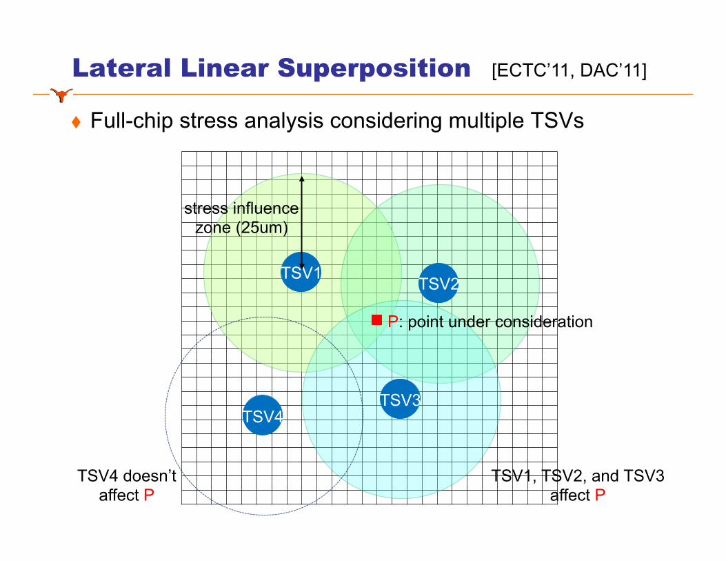
Lateral Linear Superposition
TSV1 TSV2
TSV3 TSV4
stress influence zone (25um)
P: point under consideration
TSV4 doesn’t affect P
TSV1, TSV2, and TSV3 affect P
[ECTC’11, DAC’11]
t Full-chip stress analysis considering multiple TSVs

t FEA simulation structures
› All structures undergo ∆T = -250°C of thermal load (Annealing/reflow 275°C → room temperature 25°C)
Chip-Package Co-Analysis of Stress
substrate TSV 30um device layer
30um
μ-‐bump 20um
20um
TSV
Pkg-‐bump
30um
100um
100um
TSV
Pkg-‐bump
30um
100um
μ-‐bump 20um
100um
BEOL
Back metal 5um
(a) TSV only (b) TSV + μ-‐bump
(c) TSV + pkg-‐bump (d) TSV + μ-‐bump + pkg-‐bump
underfill
underfill
device layer
device layer
device layer
TSV
[Jung et al, DAC’12]

(Lateral &) Vertical Superposition
t Stress components are added up “vertically”
LVLS works well
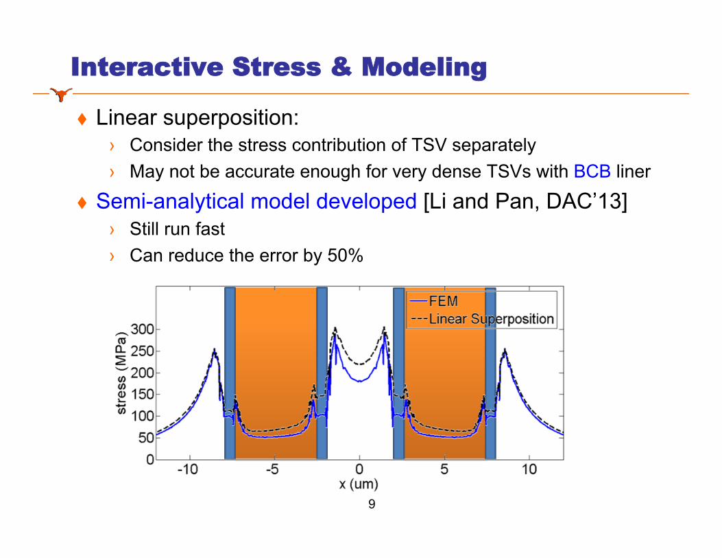
Interactive Stress & Modeling
t Linear superposition: › Consider the stress contribution of TSV separately › May not be accurate enough for very dense TSVs with BCB liner
t Semi-analytical model developed [Li and Pan, DAC’13] › Still run fast › Can reduce the error by 50%
9

Reliability/Variability Impact of Stress
1. Von Mises Reliability
2. Crack: Energy release rate (ERR)
3. Mobility/ Vth variaOon of MOS
• Von Mises Yield is function of stress tensor
• TSV stress affects ERR of TSV structure à aggravate crack
Cu shrinking d: iniOal crack length
crack propagaOon direcOon
crack front
(a) Side view
TSV
substrate
(b) Top view
liner
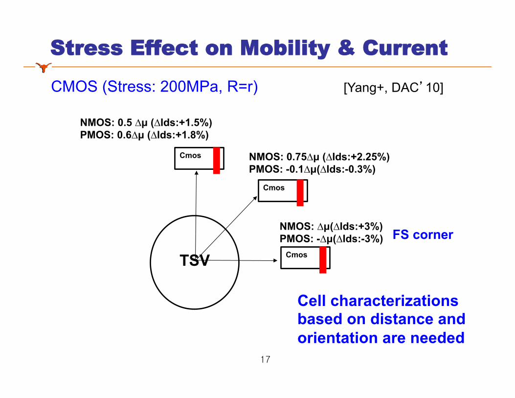
• TSV stress changes mobility of hole/electron à timing, Vth variation
(a) Hole mobility variaOon
(b) Electron mobility variaOon
(a) Von Mises stress with TSV array
(b) Von Mises stress with three TSVs
[J. Mitra et al., ECTC’11] [M. Jung et al., ICCAD’11] [J. Yang et al., DAC’10]

From Stress to Reliability t Von Mises Reliability Metric
t Physical meaning
2)σσ6(σ)σ(σ)σ(σ)σ(σ
σ2zx
2yz
2xy
2xxzz
2zzyy
2yyxx
v
+++−+−+−=
linear elastic
plastic L
strain LLΔ
=ε
ε
σv
If σv > yielding strength, deformation will be permanent and non-reversible Yielding strength - Cu: 225 ~ 600 MPa - Si: 7,000 MPa
yielding strength
∆L
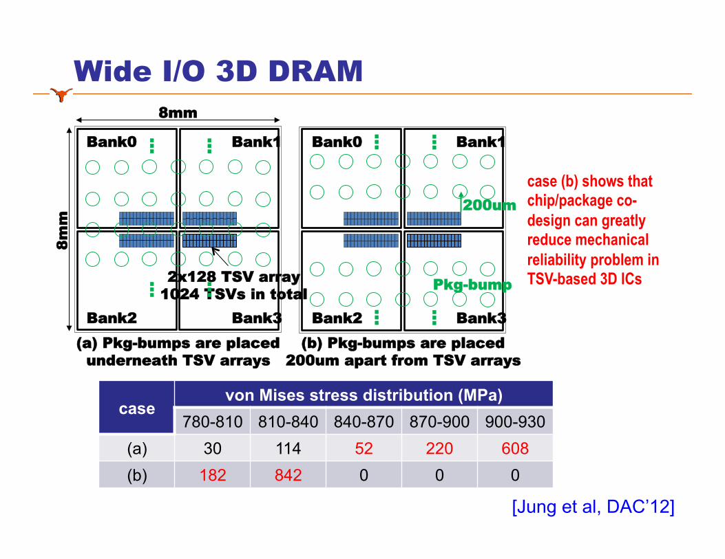
Wide I/O 3D DRAM 8mm
8m
m
Bank0 Bank1
Bank2 Bank3
2x128 TSV array 1024 TSVs in total
Bank0 Bank1
Bank2 Bank3
(a) Pkg-bumps are placed underneath TSV arrays
(b) Pkg-bumps are placed 200um apart from TSV arrays
Pkg-bump
200um
…
…
…
…
…
…
…
…
case von Mises stress distribution (MPa)
780-810 810-840 840-870 870-900 900-930 (a) 30 114 52 220 608 (b) 182 842 0 0 0
case (b) shows that chip/package co-design can greatly reduce mechanical reliability problem in TSV-based 3D ICs
[Jung et al, DAC’12]

TSV Interfacial Crack
Cu shrinking d: initial crack length
crack propagation
direction
crack front TSV
substrate
(a) Side view (b) Top view
liner
• Cu shrinks faster than Si under negative thermal load (∆T = -250°C) • Assumptions
- Crack initiates around the circumference of TSV near top surface - Crack propagates uniformly in vertically downward direction
[Jung et al, ICCAD’11]
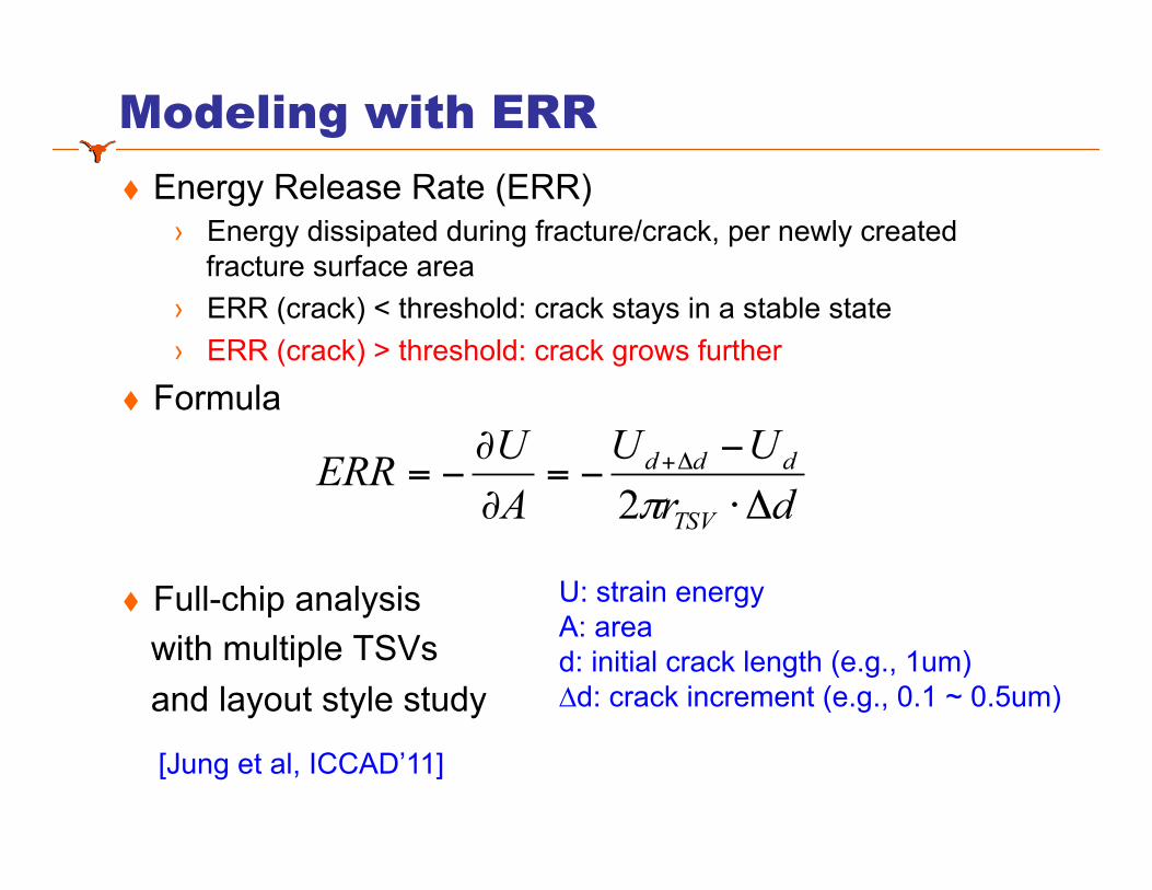
Modeling with ERR t Energy Release Rate (ERR)
› Energy dissipated during fracture/crack, per newly created fracture surface area
› ERR (crack) < threshold: crack stays in a stable state › ERR (crack) > threshold: crack grows further
t Formula
t Full-chip analysis with multiple TSVs and layout style study
drUU
AUERR
TSV
ddd
Δ⋅
−−=
∂
∂−= Δ+
π2
U: strain energy A: area d: initial crack length (e.g., 1um) ∆d: crack increment (e.g., 0.1 ~ 0.5um)
[Jung et al, ICCAD’11]

Full-Chip Crack Analysis and Study t Regular vs. irregular TSV arrays
(a) IrregA (b) RegA
(c) ERR map of IrregA (d) ERR map of RegA
100um
ERR (J/m2)
2.15 2.10 2.05 2.00 1.95 1.90 1.85 1.80
1.95 ~ 2.00
1.90 ~ 1.95

Impact of Liner
– Liner reduces ERR significantly (especially for BCB liner due to low Young’s modulus: 3 GPa, SiO2: 71 GPa)
– Thicker liner helps more by absorbing stress at TSV/liner interface – Irregular TSV placement benefits more than regular TSV placement case
(stress buffer effect of liner is effective when aggressors are close to victim TSV)
(a) Irregular vs. Regular (b) Regular w/ different KOZ A A A B
17
Stress Effect on Mobility & Current
TSV
CMOS (Stress: 200MPa, R=r)
Cmos
NMOS: 0.5 ∆µ (∆Ids:+1.5%) PMOS: 0.6∆µ (∆Ids:+1.8%)
Cmos
NMOS: ∆µ(∆Ids:+3%) PMOS: -∆µ(∆Ids:-3%)
Cmos
NMOS: 0.75∆µ (∆Ids:+2.25%) PMOS: -0.1∆µ(∆Ids:-0.3%)
Cell characterizations based on distance and orientation are needed
FS corner
[Yang+, DAC’10]
18
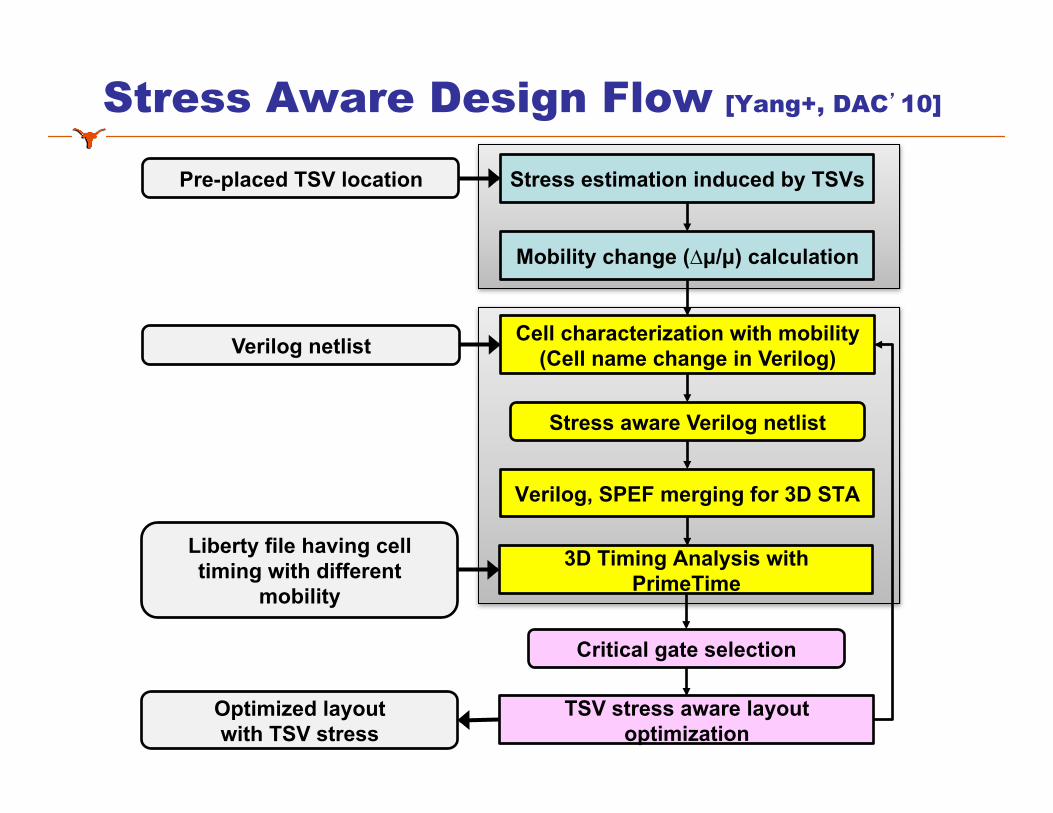
Stress Aware Design Flow [Yang+, DAC’10]
18
Stress estimation induced by TSVs
Mobility change (∆µ/µ) calculation
Verilog, SPEF merging for 3D STA
Cell characterization with mobility (Cell name change in Verilog)
TSV stress aware layout optimization
Pre-placed TSV location
Liberty file having cell timing with different
mobility
Stress aware Verilog netlist
Critical gate selection
3D Timing Analysis with PrimeTime
Optimized layout with TSV stress
Verilog netlist
19
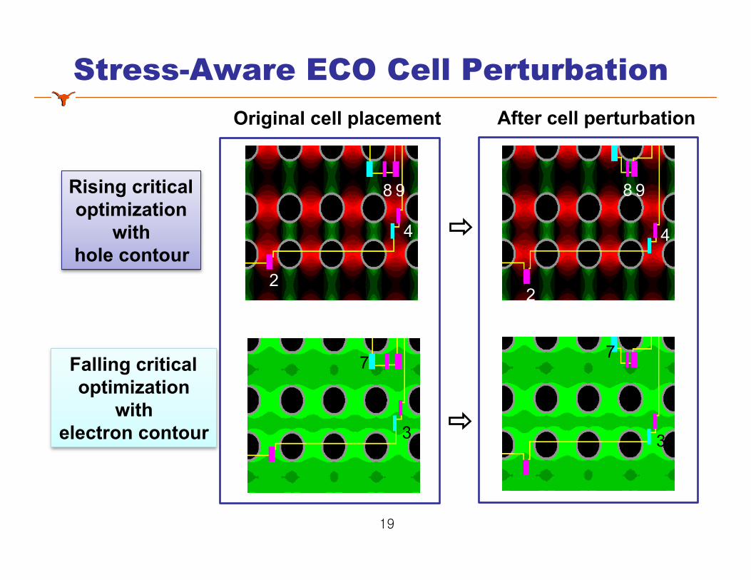
Stress-Aware ECO Cell Perturbation
3
7
2
4
8 9
3
7
2
4
8 9 Rising critical optimization
with hole contour
Falling critical optimization
with electron contour
Original cell placement After cell perturbation
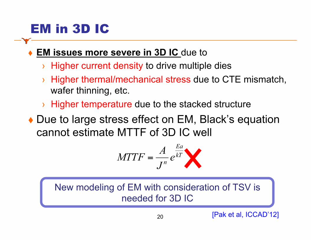
EM in 3D IC
t EM issues more severe in 3D IC due to › Higher current density to drive multiple dies › Higher thermal/mechanical stress due to CTE mismatch,
wafer thinning, etc. › Higher temperature due to the stacked structure
t Due to large stress effect on EM, Black’s equation cannot estimate MTTF of 3D IC well
20
New modeling of EM with consideration of TSV is needed for 3D IC
kTEa
n eJAMTTF =
[Pak et al, ICCAD’12]

Back to Basics t Mass balance equations solved by FEM
21
q : total atomic flux c : atomic concentration j : current density
Stress driven
Temperature grad. driven
Current density driven
Concentration grad. driven
σ : hydrostatic stress
T : temperature
0=∂
∂+⋅∇tcq
cDkTDc
TTQ
kTDcjZe
kTDcq ∇−∇Ω+
∇−= σρ

EM-Aware Routing vs. Conventional t CDF of EM-violated grids
› EM-violated grids reduced 66.4% › Wire length penalty: 0.29% › Local via penalty: 5.02%
22 [Pak et al, ICCAD’12]

Conclusion
t Reliability is a critical issue for TSV-based 3D-IC › Thermal mechanical stress › Interfacial cracking › Stress-aware EM
t Full-chip/package modeling and design issues t Need to be considered together with
› TSV array style, floorplanning, placement › Material, landing pad, and packaging › Thermal modeling › Power delivery for EM › …
23

24
Acknowledgment
t Collaboration with Prof. Sung Kyu Lim’s group at Georgia Tech
t Graduate students involved: › UT: Jiwoo Pak, Yang Li, Joydeep Mitra (also with AMD),
Jae-seok Yang (currently with Samsung) › GT: Moongon Jung, Krit Athikulwongse, Mohit Pathak
(currently with Cadence) t Support from NSF, SRC, and Sematch 3D
Enablement Center is greatly appreciated