Embed Size (px)
Citation preview
University of California
Los Angeles
Modeling and Design of STT-MRAMs
A thesis submitted in partial satisfaction
of the requirements for the degree
Master of Science in Electrical Engineering
by
Richard William Dorrance
2011

© Copyright by
Richard William Dorrance
2011
The thesis of Richard William Dorrance is approved.
Kang L. Wang
Chih-Kong Ken Yang
Dejan Markovic, Committee Chair
University of California, Los Angeles
2011
ii

To my parents
iii
Table of Contents
1 Introduction . . . . . . . . . . . . . . . . . . . . . . . . . . . . . . . . 1
1.1 Motivation for STT-MRAM . . . . . . . . . . . . . . . . . . . . . 1
1.2 Thesis Outline . . . . . . . . . . . . . . . . . . . . . . . . . . . . . 4
2 Magnetic Tunnel Junctions . . . . . . . . . . . . . . . . . . . . . . 6
2.1 Introduction to Spintronics . . . . . . . . . . . . . . . . . . . . . . 6
2.1.1 History . . . . . . . . . . . . . . . . . . . . . . . . . . . . . 7
2.1.2 Principle of Operation . . . . . . . . . . . . . . . . . . . . 8
2.1.3 Other Devices and Applications . . . . . . . . . . . . . . . 9
2.2 The Magnetic Tunnel Junction . . . . . . . . . . . . . . . . . . . 10
2.2.1 Resistance Hysteresis . . . . . . . . . . . . . . . . . . . . . 10
2.2.2 Critical Switching Current . . . . . . . . . . . . . . . . . . 12
2.2.3 Tunnel Magnetoresistance Temperature Dependency . . . 15
2.2.4 Bias Voltage Effects . . . . . . . . . . . . . . . . . . . . . . 15
2.2.5 Other Important MTJ Characteristics . . . . . . . . . . . 16
3 Modeling MTJ Characteristics . . . . . . . . . . . . . . . . . . . . 18
3.1 Modeling Dynamic Behavior . . . . . . . . . . . . . . . . . . . . . 18
3.1.1 Magnetization Dynamics . . . . . . . . . . . . . . . . . . . 18
3.1.2 Tunnel Magnetoresistance . . . . . . . . . . . . . . . . . . 21
3.2 Model Verification . . . . . . . . . . . . . . . . . . . . . . . . . . 23
3.2.1 Comparison to Measured Devices . . . . . . . . . . . . . . 23
iv
3.2.2 Comparison to Micromagnetic Simulations . . . . . . . . . 25
3.3 Statistical Characterization of MTJ Devices . . . . . . . . . . . . 26
3.3.1 MTJ Device Variability . . . . . . . . . . . . . . . . . . . . 26
3.3.2 Scaling of MTJ Current and Resistance . . . . . . . . . . . 29
4 Memory Architectures . . . . . . . . . . . . . . . . . . . . . . . . . 30
4.1 Cell Architectures . . . . . . . . . . . . . . . . . . . . . . . . . . . 30
4.1.1 1T-1MTJ . . . . . . . . . . . . . . . . . . . . . . . . . . . 30
4.1.2 Shared . . . . . . . . . . . . . . . . . . . . . . . . . . . . . 32
4.1.3 Stacked . . . . . . . . . . . . . . . . . . . . . . . . . . . . 32
4.2 Subarraying . . . . . . . . . . . . . . . . . . . . . . . . . . . . . . 33
4.2.1 1T-1MTJ . . . . . . . . . . . . . . . . . . . . . . . . . . . 33
4.2.2 Shared Architectures . . . . . . . . . . . . . . . . . . . . . 33
5 Design-Space Analysis . . . . . . . . . . . . . . . . . . . . . . . . . 37
5.1 Defining the Design Space . . . . . . . . . . . . . . . . . . . . . . 37
5.2 Sensitivity Analysis and Design Example . . . . . . . . . . . . . . 41
5.2.1 Design-Space Sensitivity Analysis . . . . . . . . . . . . . . 42
5.2.2 Design Example . . . . . . . . . . . . . . . . . . . . . . . . 43
5.3 Future Scalability . . . . . . . . . . . . . . . . . . . . . . . . . . . 45
6 Memory Design . . . . . . . . . . . . . . . . . . . . . . . . . . . . . 48
6.1 MTJ/CMOS Integration . . . . . . . . . . . . . . . . . . . . . . . 48
6.2 Test Chips . . . . . . . . . . . . . . . . . . . . . . . . . . . . . . . 50
v

6.2.1 90nm Bulk CMOS . . . . . . . . . . . . . . . . . . . . . . 50
6.2.2 65nm Bulk CMOS . . . . . . . . . . . . . . . . . . . . . . 50
6.2.3 45nm SOI CMOS . . . . . . . . . . . . . . . . . . . . . . . 53
6.2.4 Design Comparison . . . . . . . . . . . . . . . . . . . . . . 54
7 Conclusion . . . . . . . . . . . . . . . . . . . . . . . . . . . . . . . . . 56
7.1 Summary of Research Contributions . . . . . . . . . . . . . . . . 56
7.2 Future Work . . . . . . . . . . . . . . . . . . . . . . . . . . . . . . 57
References . . . . . . . . . . . . . . . . . . . . . . . . . . . . . . . . . . . 58
vi
List of Figures
1.1 Comparison of memory technologies. . . . . . . . . . . . . . . . . 2
1.2 SEM photo of an MTJ. . . . . . . . . . . . . . . . . . . . . . . . . 3
1.3 MTJ in (a) parallel and (b) antiparallel configuration. . . . . . . . 4
2.1 Spintronic operation of a spin polarizer. . . . . . . . . . . . . . . . 8
2.2 Spintronic operation of a spin filter. . . . . . . . . . . . . . . . . . 8
2.3 Resistance hysteresis of an MTJ. . . . . . . . . . . . . . . . . . . 11
2.4 MTJ switching regimes. . . . . . . . . . . . . . . . . . . . . . . . 13
2.5 Switching probability vs. pulse duration. . . . . . . . . . . . . . . 14
3.1 Sketch of basic MTJ structure. . . . . . . . . . . . . . . . . . . . 19
3.2 Efficiency factor of spin-polarization vs. θ. . . . . . . . . . . . . . 20
3.3 Normalized magnetization saturation. . . . . . . . . . . . . . . . . 22
3.4 Fitted MTJ parameters. . . . . . . . . . . . . . . . . . . . . . . . 23
3.5 TMR vs. temperature. . . . . . . . . . . . . . . . . . . . . . . . . 24
3.6 TMR vs. bias voltage. . . . . . . . . . . . . . . . . . . . . . . . . 24
3.7 R-H hysteresis. . . . . . . . . . . . . . . . . . . . . . . . . . . . . 25
3.8 Process flow for evaluating Verilog-A model. . . . . . . . . . . . . 26
3.9 Resistance vs. time. . . . . . . . . . . . . . . . . . . . . . . . . . . 27
3.10 Measured MTJ devices. . . . . . . . . . . . . . . . . . . . . . . . . 28
3.11 MTJ free layer dimensions. . . . . . . . . . . . . . . . . . . . . . . 29
4.1 1T-1MTJ memory cell architectures. . . . . . . . . . . . . . . . . 31
vii
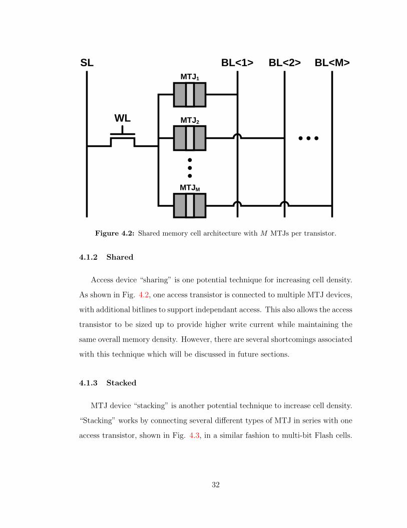
4.2 Shared memory cell architecture. . . . . . . . . . . . . . . . . . . 32
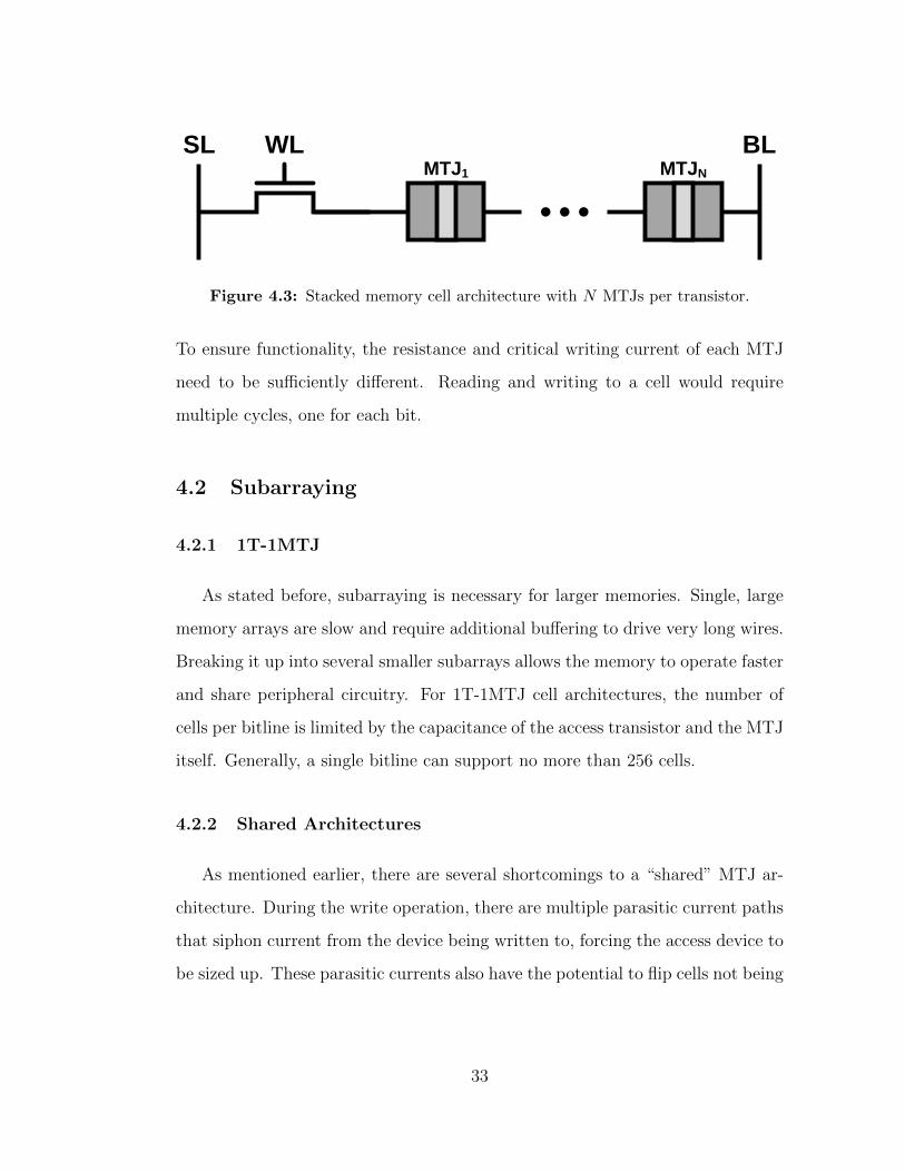
4.3 Stacked memory cell architecture. . . . . . . . . . . . . . . . . . . 33
4.4 Shared architecture with subarraying. . . . . . . . . . . . . . . . . 34
4.5 Worst-case writing configurations for sharing. . . . . . . . . . . . 36
5.1 Conventional MTJ switching currents. . . . . . . . . . . . . . . . 38
5.2 Definition of the design space. . . . . . . . . . . . . . . . . . . . . 39
5.3 TMRMIN vs. ∆Iref/Iref . . . . . . . . . . . . . . . . . . . . . . . . 40
5.4 IC vs. WN vs. RMAX . . . . . . . . . . . . . . . . . . . . . . . . . 41
5.5 Design space example for a 65nm process. . . . . . . . . . . . . . 44
5.6 Design-space sensitivity example for a 65nm process. . . . . . . . 45
5.7 Design margin vs. technology node. . . . . . . . . . . . . . . . . . 46
6.1 MTJ/CMOS integration at M4. . . . . . . . . . . . . . . . . . . . 49
6.2 Block diagram of the 90nm test chip. . . . . . . . . . . . . . . . . 51
6.3 Read/Write driver for short-pulse reading. . . . . . . . . . . . . . 52
6.4 Cadence layout of the 65nm test chip. . . . . . . . . . . . . . . . . 53
6.5 Cadence layout of the 45nm test chip. . . . . . . . . . . . . . . . . 54
6.6 Design comparison of STT-MRAMs. . . . . . . . . . . . . . . . . 55
viii
List of Tables
3.1 Measured device statistics. . . . . . . . . . . . . . . . . . . . . . . 28
5.1 JC(P → AP ) for an RA of 5 Ω · µm2 . . . . . . . . . . . . . . . . 47
5.2 JC(P → AP ) for an RA of 10 Ω · µm2 . . . . . . . . . . . . . . . 47
5.3 JC(P → AP ) for an RA of 15 Ω · µm2 . . . . . . . . . . . . . . . 47
6.1 Time to read RP (90nm) . . . . . . . . . . . . . . . . . . . . . . . 52
6.2 Time to read RAP (90nm) . . . . . . . . . . . . . . . . . . . . . . 52
ix
Acknowledgments
First, I would like to thank my advisor, Professor Dejan Markovic, without
whom this thesis could never have been written. I am sincerely grateful for the
help and support he has given me through the course of this work. I would also
like to acknowledge Professors Chih-Kong Ken Yang and Kang L. Wang and
Dr. Pedram Khalili. Professor Yang’s knowledge and experience in designing
memories was instrumental to this project. Without the help and insight of
Professor Wang and Dr. Khalili I could never have comprehended the physics of
spintroncs half as well as I do now.
This work could not have progressed without the infrastructure and support
provided by research group. I would like to whole heartedly thank Henry Chen,
Kevin Dwan, and Yuta Toriyama for their help in the editing of this manuscript.
I would also like to thank the rest of the STT-RAM circuits design team. With-
out their hard work and dedication, this project could never have gotten off the
ground. I would also like to thank graduate students Juan G. Alzate, Pramey
Upadhyaya, and Mark Lewis from the STT-RAM MTJ design team. They pro-
vided an extensive number of device characterizations and simulations for the
development of my MTJ macro-model.
Most of all, I would like to thank my parents, Gary Dorrance and Karen
Lawrence, for all the love and support they have provided over the years. Not
the least of which included the editing of early drafts of this thesis. Last, but
certainly not least, I would like to thank the mighty Tyrannosaurus Rex, king of
the dinosaurs. May he live on in the hopes and dreams of a man still a boy at
heart.
x
Abstract of the Thesis
Modeling and Design of STT-MRAMs
by
Richard William Dorrance
Master of Science in Electrical Engineering
University of California, Los Angeles, 2011
Professor Dejan Markovic, Chair
Spin-Torque Transfer Magnetoresistive Random Access Memory (STT-
MRAM) is an emerging memory technology with the potential to become a true
universal memory: the density of DRAM, the speed of SRAM, and the non-
volatility of Flash. STT-MRAM uses a Magnetic Tunnel Junction (MTJ) device
as a non-volatile magnetic memory storage element and the recently discovered
spin-torque phenomenon to switch magnetic states. In this work, the fundamental
quantum mechanical nature of the MTJ is explored to develop a highly accurate
physics-based model of its spintronic operation. Innovative design-space analy-
sis techniques are introduced to investigate existing and proposed STT-MRAM
architectures. Three test chips were fabricated using these new design methodolo-
gies at 90nm, 65nm, and 45nm technology nodes. Each chip has a memory density
more than two times greater and a read/write performance more than 10 times
greater when compared to published state-of-the-art STT-MRAMs. Theoretical
and observed scaling trends show flash-like densities, with SRAM-equivalent ac-
cess times, while using 10 times less energy in more advanced technology nodes
(below 32nm).
xi
CHAPTER 1
Introduction
STT-MRAM1 is an emerging memory technology that exploits the recently
discovered phenomena of spin-torque transfer (STT) in MTJs. This chapter
provides a brief motivation for STT-MRAM, as well as outlines the rest of the
thesis.
1.1 Motivation for STT-MRAM
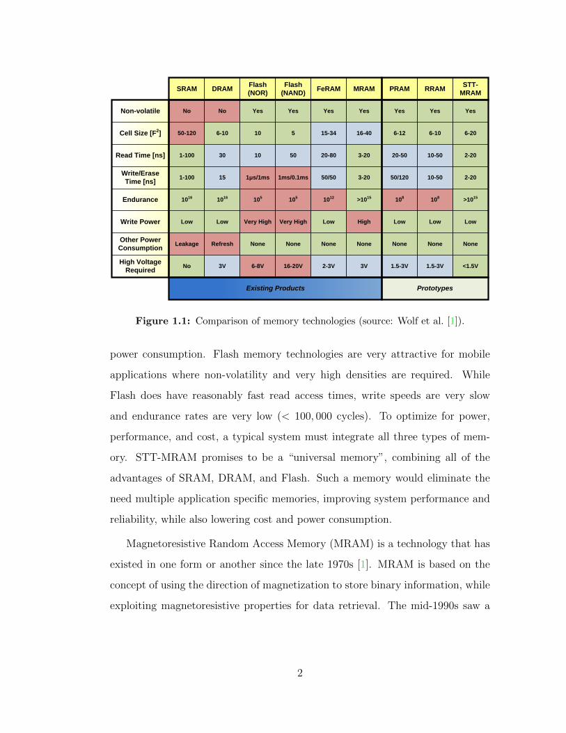
Currently, three types of memory exist, with each technology doing a single
thing very well: Static RAM (SRAM), Dynamic RAM (DRAM), and Flash mem-
ory. SRAM has excellent read and write speeds, but has a very large cell size
(requiring 6 or more transistors per cell). The speed of SRAM makes it ideally
suited for embedded applications, particularly cache memory, where performance
is more important than memory density. SRAM is volatile, but requires very little
active power for data retention. DRAM is able to provide much better memory
density through its use of a single transistor with a storage capacitor. However,
charge tends to leak off of the capacitor, requiring a power hungry refresh cycle
every few milliseconds. DRAM is typically used as the main system memory in
a computer, where memory density and performance are more important than
1In literature, Spin-Torque Transfer Random Access Memory (STT-RAM) and Spin RandomAccess Memory (SPRAM) are used interchangeably with STT-MRAM. However, STT-MRAMis more common and is, therefore, used exclusively in this thesis.
1
SRAM DRAMFlash
(NOR)
Flash
(NAND)FeRAM MRAM PRAM RRAM
STT-
MRAM
Non-volatile
Cell Size [F2]
Read Time [ns]
Write/Erase
Time [ns]
Endurance
Write Power
Other Power
Consumption
High Voltage
Required
Existing Products Prototypes
No No Yes Yes Yes Yes Yes Yes Yes
50-120
1-100
1-100
1016
Low
No
Leakage
6-10
30
15
1016
Low
3V
Refresh
10
10
1μs/1ms
105
Very High
6-8V
None
5
50
1ms/0.1ms
105
Very High
16-20V
None
15-34
20-80
50/50
1012
Low
2-3V
None
16-40
3-20
3-20
>1015
High
3V
None
6-12
20-50
50/120
108
Low
1.5-3V
None
6-10
10-50
10-50
108
Low
1.5-3V
None
6-20
2-20
2-20
>1015
Low
<1.5V
None
Figure 1.1: Comparison of memory technologies (source: Wolf et al. [1]).
power consumption. Flash memory technologies are very attractive for mobile
applications where non-volatility and very high densities are required. While
Flash does have reasonably fast read access times, write speeds are very slow
and endurance rates are very low (< 100, 000 cycles). To optimize for power,
performance, and cost, a typical system must integrate all three types of mem-
ory. STT-MRAM promises to be a “universal memory”, combining all of the
advantages of SRAM, DRAM, and Flash. Such a memory would eliminate the
need multiple application specific memories, improving system performance and
reliability, while also lowering cost and power consumption.
Magnetoresistive Random Access Memory (MRAM) is a technology that has
existed in one form or another since the late 1970s [1]. MRAM is based on the
concept of using the direction of magnetization to store binary information, while
exploiting magnetoresistive properties for data retrieval. The mid-1990s saw a
2
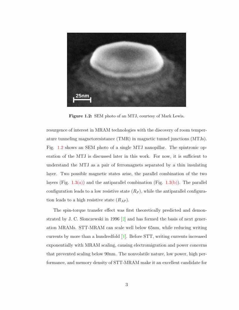
25nm
Figure 1.2: SEM photo of an MTJ, courtesy of Mark Lewis.
resurgence of interest in MRAM technologies with the discovery of room temper-
ature tunneling magnetoresistance (TMR) in magnetic tunnel junctions (MTJs).
Fig. 1.2 shows an SEM photo of a single MTJ nanopillar. The spintronic op-
eration of the MTJ is discussed later in this work. For now, it is sufficient to
understand the MTJ as a pair of ferromagnets separated by a thin insulating
layer. Two possible magnetic states arise, the parallel combination of the two
layers (Fig. 1.3(a)) and the antiparallel combination (Fig. 1.3(b)). The parallel
configuration leads to a low resistive state (RP ), while the antiparallel configura-
tion leads to a high resistive state (RAP ).
The spin-torque transfer effect was first theoretically predicted and demon-
strated by J. C. Slonczewski in 1996 [2] and has formed the basis of next gener-
ation MRAMs. STT-MRAM can scale well below 65nm, while reducing writing
currents by more than a hundredfold [1]. Before STT, writing currents increased
exponentially with MRAM scaling, causing electromigration and power concerns
that prevented scaling below 90nm. The nonvolatile nature, low power, high per-
formance, and memory density of STT-MRAM make it an excellent candidate for
3
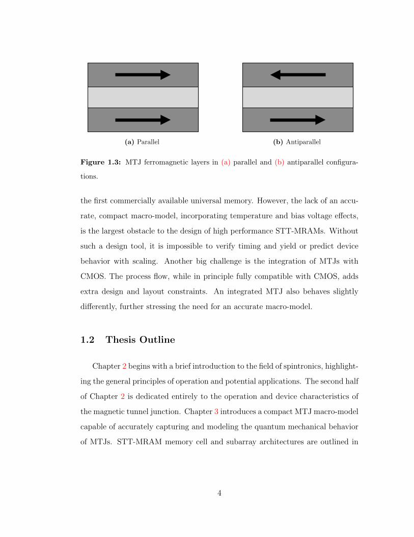
(a) Parallel (b) Antiparallel
Figure 1.3: MTJ ferromagnetic layers in (a) parallel and (b) antiparallel configura-
tions.
the first commercially available universal memory. However, the lack of an accu-
rate, compact macro-model, incorporating temperature and bias voltage effects,
is the largest obstacle to the design of high performance STT-MRAMs. Without
such a design tool, it is impossible to verify timing and yield or predict device
behavior with scaling. Another big challenge is the integration of MTJs with
CMOS. The process flow, while in principle fully compatible with CMOS, adds
extra design and layout constraints. An integrated MTJ also behaves slightly
differently, further stressing the need for an accurate macro-model.
1.2 Thesis Outline
Chapter 2 begins with a brief introduction to the field of spintronics, highlight-
ing the general principles of operation and potential applications. The second half
of Chapter 2 is dedicated entirely to the operation and device characteristics of
the magnetic tunnel junction. Chapter 3 introduces a compact MTJ macro-model
capable of accurately capturing and modeling the quantum mechanical behavior
of MTJs. STT-MRAM memory cell and subarray architectures are outlined in
4

Chapter 4, with design-space analysis techniques introduced in Chapter 5. The
analysis techniques introduced in Chapter 5 are used in Chapter 6 in the design of
three separate STT-MRAM memory chips at 90nm, 65nm, and 45nm technology
nodes. Finally, Chapter 7 presents ongoing and future work, and concludes the
thesis.
5
CHAPTER 2
Magnetic Tunnel Junctions
The focus of this chapter is to introduce the MTJ device, as well as the field
of spintronics. The first section provides a brief background on spintronics—
its history and fundamental physical operation. Alternative devices (e.g. spin
FETs, MBTs, and spin LEDs) and applications are discussed before defining the
characteristics and unique properties of the MTJ device.
2.1 Introduction to Spintronics
Spintronics, the amalgamation of the words “spin” and “electronics,” involves
the active control and manipulation of electron spin in solid-state electronics [3].
In traditional electronic devices, information processing works on the principle of
control over the flow of charge through a semiconductor material. Large scale,
non-volatile memories (e.g., hard disk drives or HDDs) exploit ferromagnetism to
store information by forcing the spin alignment of many electrons [4]. Spintronics,
as a whole, aims to merge information processing and storage through the use of
spin-polarized currents [1].
6
2.1.1 History
Early work into spintronics began in the mid-1930s with the discovery of
unusual resistance behavior in ferromagnetic materials at extremely low temper-
atures [3]. Electron tunneling measurements played a key role in early experi-
mental work, with several key experiments in the early 1970s demonstrating the
viability of spin filters (discussed later). In 1975, Julliere [5] formulated his now-
famous conductance model describing the change of conductance between the
parallel and antiparallel states of an MTJ. However, it wasn’t until the mid-to-
late 1980s that the room temperature magnetoresistive effects were discovered.
Anisotropic magnetoresistive (AMR) layers were first used to construst AMR-
MRAM to replace bulky and heavy plated-wire radiation-hard memories [1].
AMR was quickly replaced by the discovery of giant magnetoresistance (GMR)
in 1988 [6]. Since the discovory of GMR, electron spin has formed the basis of
almost all electronic information storage [7].
In the early 1990s, MTJ materials with higher TMRs (on the order of 20%
at room temperature) were discovered [1]. Since then, MTJ structures (using
MgO insulating barriers) with TMRs on the order of 1000% have been demon-
strated at room temperature [8]. Within ten years of its discovery, spintronics has
grown into a billion dollar industry, with commercial sales exceeding $3 billion
in 2005 [6]. Despite these successes, spin injection from ferromagnetic layers into
semiconductors remains a significant bottleneck in semiconductor-based spintron-
ics. Recently, much emphasis has been placed in trying to induce ferromagnetism
in a semiconductors to produce dilute magnetic semiconductors (DMS) [7]. DMS
has the potential to improve the Curie temperature and magnetic bandgap of
future spintronic devices [9].
7
(1) (3)
(2)
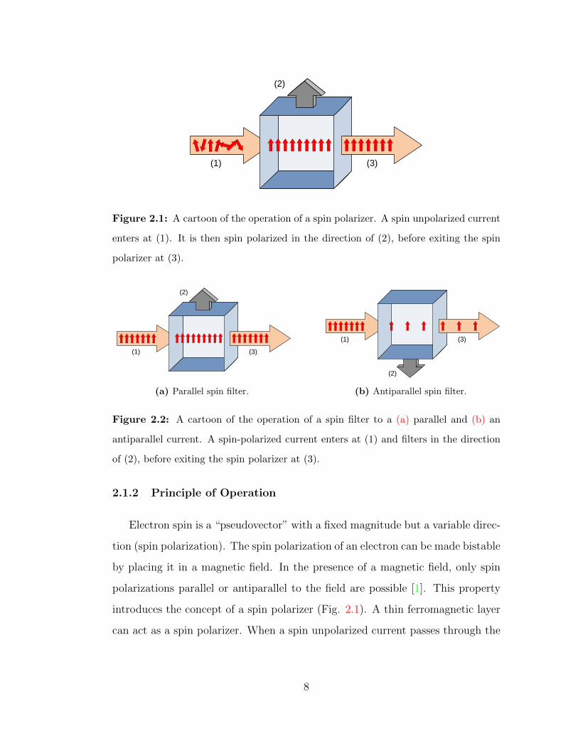
Figure 2.1: A cartoon of the operation of a spin polarizer. A spin unpolarized current
enters at (1). It is then spin polarized in the direction of (2), before exiting the spin
polarizer at (3).
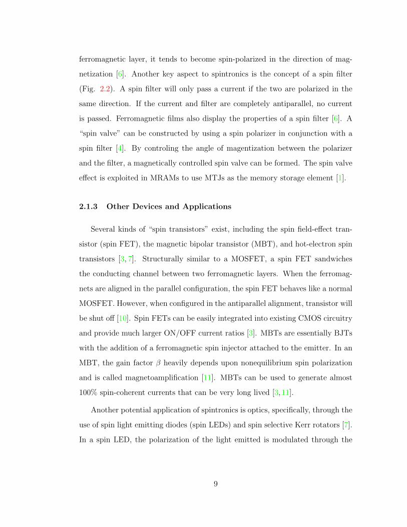
(1) (3)
(2)
(a) Parallel spin filter.
(1) (3)
(2)
(b) Antiparallel spin filter.
Figure 2.2: A cartoon of the operation of a spin filter to a (a) parallel and (b) an
antiparallel current. A spin-polarized current enters at (1) and filters in the direction
of (2), before exiting the spin polarizer at (3).
2.1.2 Principle of Operation
Electron spin is a “pseudovector” with a fixed magnitude but a variable direc-
tion (spin polarization). The spin polarization of an electron can be made bistable
by placing it in a magnetic field. In the presence of a magnetic field, only spin
polarizations parallel or antiparallel to the field are possible [1]. This property
introduces the concept of a spin polarizer (Fig. 2.1). A thin ferromagnetic layer
can act as a spin polarizer. When a spin unpolarized current passes through the
8
ferromagnetic layer, it tends to become spin-polarized in the direction of mag-
netization [6]. Another key aspect to spintronics is the concept of a spin filter
(Fig. 2.2). A spin filter will only pass a current if the two are polarized in the
same direction. If the current and filter are completely antiparallel, no current
is passed. Ferromagnetic films also display the properties of a spin filter [6]. A
“spin valve” can be constructed by using a spin polarizer in conjunction with a
spin filter [4]. By controling the angle of magentization between the polarizer
and the filter, a magnetically controlled spin valve can be formed. The spin valve
effect is exploited in MRAMs to use MTJs as the memory storage element [1].
2.1.3 Other Devices and Applications
Several kinds of “spin transistors” exist, including the spin field-effect tran-
sistor (spin FET), the magnetic bipolar transistor (MBT), and hot-electron spin
transistors [3, 7]. Structurally similar to a MOSFET, a spin FET sandwiches
the conducting channel between two ferromagnetic layers. When the ferromag-
nets are aligned in the parallel configuration, the spin FET behaves like a normal
MOSFET. However, when configured in the antiparallel alignment, transistor will
be shut off [10]. Spin FETs can be easily integrated into existing CMOS circuitry
and provide much larger ON/OFF current ratios [3]. MBTs are essentially BJTs
with the addition of a ferromagnetic spin injector attached to the emitter. In an
MBT, the gain factor β heavily depends upon nonequilibrium spin polarization
and is called magnetoamplification [11]. MBTs can be used to generate almost
100% spin-coherent currents that can be very long lived [3, 11].
Another potential application of spintronics is optics, specifically, through the
use of spin light emitting diodes (spin LEDs) and spin selective Kerr rotators [7].
In a spin LED, the polarization of the light emitted is modulated through the
9
application of an external magnetic field [12]. Variable polarized LEDs promise
to provide more energy efficient displays and significantly higher signal-to-noise
ratio (SNR) in optical communications [7]. A Kerr rotator takes advantage of the
magneto-optic Kerr effect (MOKE), the unique optically-reflective properties of
magnetic materials, to manipulate the polarity of reflected light. Traditionally,
Kerr rotators have many applications in the microscopic imaging of magnetic
domains, magnetic media, and terahertz lasers [13]. A spin selective rotator,
with the application of a bias voltage, can be made to reflect incident light either
with or without a large Kerr rotation angle [7].
2.2 The Magnetic Tunnel Junction
This section is intended to describe the major device characteristics observed
in MTJs. The science responsible for each effect, as well as their importance to
the MTJ model, is discussed.
2.2.1 Resistance Hysteresis
The large resistance hysteresis present in MTJs makes them very well-suited
as a non-volatile memory element. The source of this hysteresis is very nicely
explained by the spin-valve structure of an MTJ [3]. As mentioned before in
Fig. 3.1, an MTJ consists of a thin insulating layer sandwiched between two fer-
romagnetic layers. The electromagnetic dynamics of the system allows for only
two possible states: parallel or antiparallel [6]. The two ferromagnetic layers are
magnetized in the same direction while in the parallel state and in the oppo-
site directions while in the antiparallel state. When a current flows through the
MTJ, one ferromagnetic layer acts as a spin polarizer and the other as a spin
10
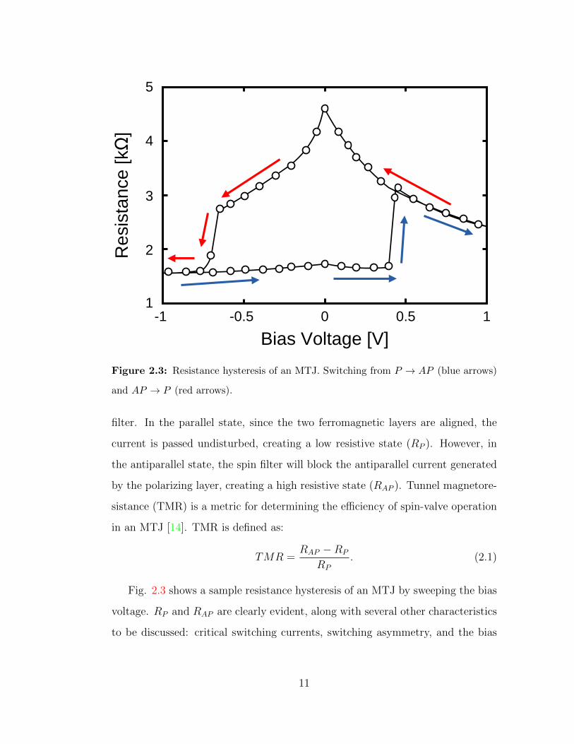
Re
sis
tan
ce
[kΩ
]
Bias Voltage [V]
-1 -0.5 0 0.5 11
2
3
4
5
Figure 2.3: Resistance hysteresis of an MTJ. Switching from P → AP (blue arrows)
and AP → P (red arrows).
filter. In the parallel state, since the two ferromagnetic layers are aligned, the
current is passed undisturbed, creating a low resistive state (RP ). However, in
the antiparallel state, the spin filter will block the antiparallel current generated
by the polarizing layer, creating a high resistive state (RAP ). Tunnel magnetore-
sistance (TMR) is a metric for determining the efficiency of spin-valve operation
in an MTJ [14]. TMR is defined as:
TMR =RAP −RP
RP
. (2.1)
Fig. 2.3 shows a sample resistance hysteresis of an MTJ by sweeping the bias
voltage. RP and RAP are clearly evident, along with several other characteristics
to be discussed: critical switching currents, switching asymmetry, and the bias
11
voltage dependance of TMR.
2.2.2 Critical Switching Current
2.2.2.1 Asymmetric Switching Currents
It should be noted that the critical switching currents are asymmetric, with
IC(P → AP ) > IC(AP → P ) [15]. This effect was predicted by Slonczewski [2]
with his discovery of the spin-torque transfer phenomena. This asymmetry is
proportional to and increases linearly with TMR [16]. The simplest explanation
of this behavior is that the antiparallel configuration is a lower energy state than
the parallel case [3], making it is easier to switch to the antiparallel state than
the parallel state. Several techniques exist to minimize the asymmetry. Lee et
al. [17] were able to tune the magnetostatic offset field (using an external magnetic
field) with exceptional results, reducing the asymmetric current ratio from 1.51
to 1.04. Yao et al. [18] were able to reduce the offset from 1.50 to 1.28 with the
introduction of a nanocurrent-channel layer to the MTJ stack.
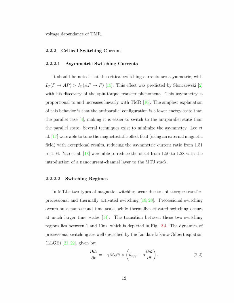
2.2.2.2 Switching Regimes
In MTJs, two types of magnetic switching occur due to spin-torque transfer:
precessional and thermally activated switching [19, 20]. Precessional switching
occurs on a nanosecond time scale, while thermally activated switching occurs
at much larger time scales [14]. The transition between these two switching
regions lies between 1 and 10ns, which is depicted in Fig. 2.4. The dynamics of
precessional switching are well described by the Landau-Lifshitz-Gilbert equation
(LLGE) [21,22], given by:
∂ ~m
∂t= −γMS ~m×
(~heff − α
∂ ~m
∂t
). (2.2)
12
Precessional
Switching
(T < 10ns)
Thermally Activated
Switching
(T > 10ns)
10-1
100
101
102
103
104
105
0
2
4
6
8
10
12
Pulse Width τ [ns]
Cri
tic
al C
urr
en
t D
en
sit
y J
C [
MA
/cm
2]
Figure 2.4: MTJ switching regimes.
Equation 2.2, with the addition of Slonczewski’s spin-torque transfer term [2],
will be discussed in much more detail in Chapter 3.
Switching occurs on much longer time scale when the current though the MTJ
is less than the critical switching current [19]. In the thermally activated regime,
the switching current is a function of pulse duration τ :
IC = IC0
[1− ln (τ/τ0)
∆
], (2.3)
where ∆ is the thermal stability of the MTJ, τ0 is the natural time constant, and
IC0 is the critical switching current [23].
13
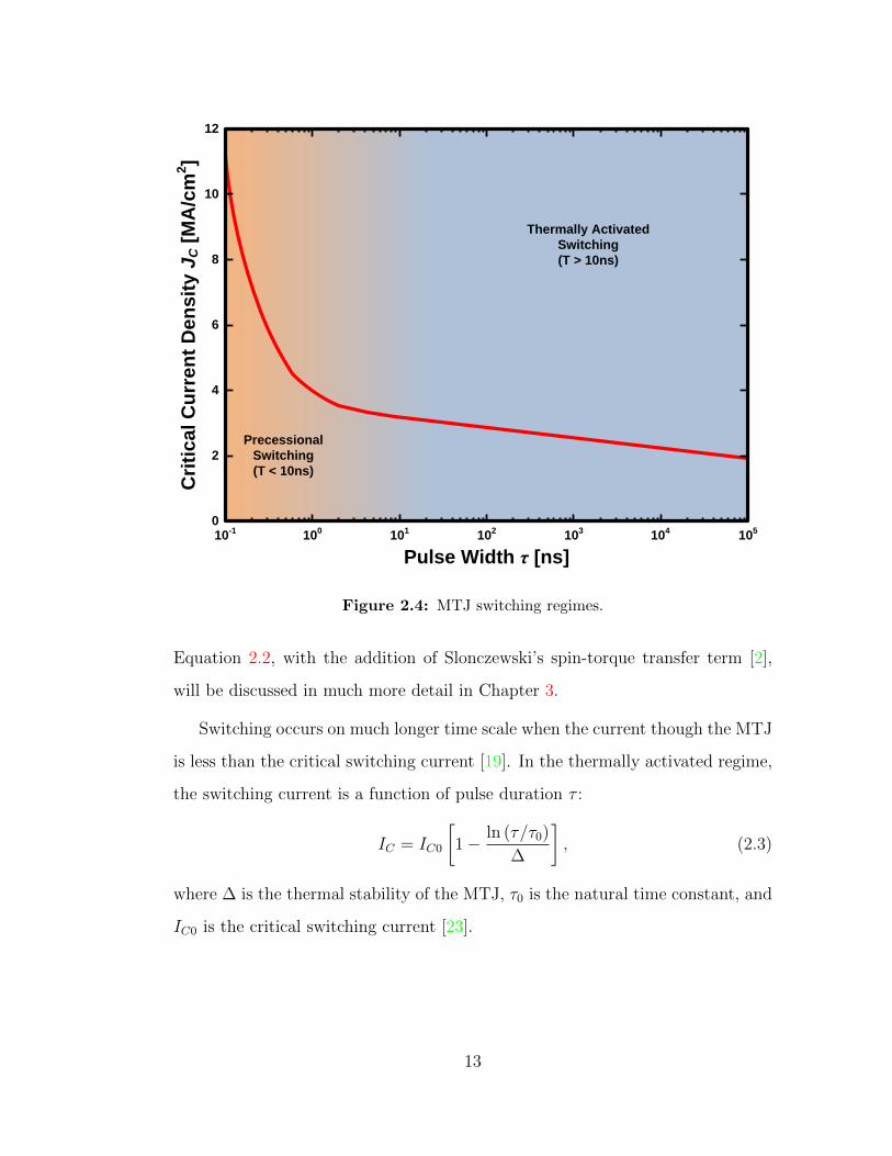
Figure 2.5: Switching probability vs. pulse duration for (a) P → AP and (b) AP →
P . Reproduced with permission from Zeng et al. [24].
2.2.2.3 Probabilistic Switching
Due to thermal agitation, the inital angle between the magnetizations of the
fixed and free layers are in constant flux [25]. Combined with other finite tem-
perature effects, this leads to a time-varying critical switching current [26]. This
effect is very well modeled as a single critical switching current with a probabilis-
tic distribution [27]. Fig. 2.5 shows one such measurement of the probabilistic
distribution for a 135 × 65nm2 CoFeB/MgO/CoFeB device. For memory appli-
cations, devices exhibiting very sharp transitions are highly desirable [28].
14
2.2.3 Tunnel Magnetoresistance Temperature Dependency
The sensitivity of TMR to temperature is well documented in literature [5,
29–32]. The effect at zero bias voltage is very well described by the Julliere
conductance model [29]. The Julliere model decomposes the conductance of the
MTJ into two parts: (i) GT , the conductance due to direct elastic tunneling, and
(ii) GSI , the conductance due to imperfections in the insulating layer (assumed
to be unpolarized). The total conductance (G), as a function of the angle θ is
given by:
G (θ) = GT 1 + P1P2 cos (θ)+GSI , (2.4)
where P1 and P2 are the factors of spin-polarization for the two ferromagnetic
layers, and θ = 0 for parallel and θ = 180 for anti-parallel magnetization. The
temperature dependance of spin-polarazation has been extensively studied and
shown to be:
P (T ) = P0
(1− αspT 3/2
). (2.5)
It should be noted that variations in GT due to temperature are almost negligible,
whereas GSI ∝ T 4/3 has been confirmed both theoretically and experimentally
[33].
2.2.4 Bias Voltage Effects
The Julliere conductance model is not perfect, being only able predict TMR
at zero bias voltage [30]. Fig. 2.3 illustrates the effect of the so called “zero bias
anomaly” in an MTJ structure [34]. The source of the bias voltage dependence of
TMR is still not very well understood [35]. However, it is suspected that elastic
currents play a role at low voltages [36] and redistribtion of the density of states
at higher voltages [35]. At higher voltages, Simmons’ formula can be used to
15
model the density of states to predict degradation of TMR to a bias voltage [31].
2.2.5 Other Important MTJ Characteristics
2.2.5.1 Self Induced Heating
Due to small device sizes and large write currents, the power density of a
write operation in an MTJ can be very high. These high power densities can
lead to localized heating or self induced heating in MTJs [37]. Hotspots (weak
areas in the insulating barrier) and pinholes (direct contact between the mag-
netic layers) cause nonuniform current flow through the MTJ [38]. This leads
to nonuniform heating across the tunneling barrier, affecting spin-polarization
efficiency and causing inelastic electron scattering [38]. Simulations show that
consecutive write opperations produce a 9-15°C increase in the temperature of
the MTJ [37]. Additionally, a large number of writes followed by a read leads to
degraded sensing margin. Self induced heating is exploited as the writing mech-
anism in Thermal Assisted Switching MRAMs (TAS-MRAMs) [39]. However, in
STT-MRAMS, lower RAs are generally used to avoid self induced heating [37].
2.2.5.2 Backhopping
Backhopping is a recently discovered phenomenon, whereby increasing the
bias voltage beyond the apparent switching threshold causes the MTJ to pre-
cess back and forth before settling to its original state [40]. This results in a
lowered probability of switching at bias voltages beyond the threshold, causing
non-monotonicity in the probability switching curves [41]. Backhopping is also
much more pronounced in switching from an antiparallel to a parallel state [40,41].
This suggests that backhopping is related to the interlayer exchange coupling be-
16
tween the free and fixed layers. Backhopping is more pronounced on longer time
scales, where self induced heating could be lowering the thermal energy barrier
and causing hot-electron events [40]. Another explanation is that certain noise
processes (discussed in the next section) might be responsible [41].
2.2.5.3 Noise
Many different mechanisms are responsible for noise in MTJs. Among these
are thermal noise (Johnson-Nyquist), shot noise (current), flicker noise (1/f),
random telegraph noise (RTN), and noise due to charge-trapping in the oxide
barrier [28,42–45]. Due to the strong coupling between magnetization and junc-
tion resistance in MTJs, noise in the magnetic domain is responsible for random
resistance fluctuations [42]. These resistance fluctuations are responsible for 1/f
noise as well as RTN [45]. Magnetic impurities inside the tunneling barrier are
responsible for charge-trapping [42].
Thermal noise dominates at low bias voltages before quickly being overpow-
ered by shot noise [44]. At room temperatures, shot noise typically dominates
for bias voltages greater than 50mV [43]. The thermal noise of an MTJ is given
by SV = 4kBTRMTJ , where kB is Boltzmann’s constant, T is in Kelvin, and
RMTJ is the resistance of the MTJ [28]. Similarly, shot noise can be expressed as
SV = 2eIR2MTJ , where e is the charge of an electron and I is the current through
the device [28].
Another significant contribution to low-frequency noise is due to domain wall
hopping between pinning sites [28, 42]. These pinning sites are created by edge
roughness, interface defects, bulk defects, and random film anisotropy [42]. The
low-frequency noise characteristics of an MTJ can be significantly reduced by
improving the smoothness of the ferromagnetic/insulator interface [45].
17
CHAPTER 3
Modeling MTJ Characteristics
Recent advances in MgO-based MTJs show strong potential for STT-MRAMs
[46]. STT-MRAM has the potential to rival the densities of DRAM, the speed
of SRAM, and is non-volatile without degrading over time like Flash [47]. The
greatest hindrance in the design of STT-MRAM, and other spintronics circuits,
is the lack of a compact MTJ model capable of accurately modeling temperature
and voltage dependencies. Capturing these dependencies, in a compact model
compatible with circuit simulators, is crucial for performing accurate Monte
Carlo simulations to place yield and performance bounds on STT-MRAM. This
chapter presents such a model implemented in Verilog-A. The model’s simula-
tion results were also compared to a model implemented using the LLG Micro-
magnetics Simulator [48] and actual device measurements from 135nm by 65nm
CoFeB/MgO/CoFeB MTJs.
3.1 Modeling Dynamic Behavior
3.1.1 Magnetization Dynamics
The precessional motion of magnetization ( ~M) of the free layer of a MTJ, in
the presence of an external magnetic field ( ~Heff ), can be very accurately modeled
by the LLGE, Eq. 2.2 [23]. With the introduction of Slonczewski’s spin-torque
18
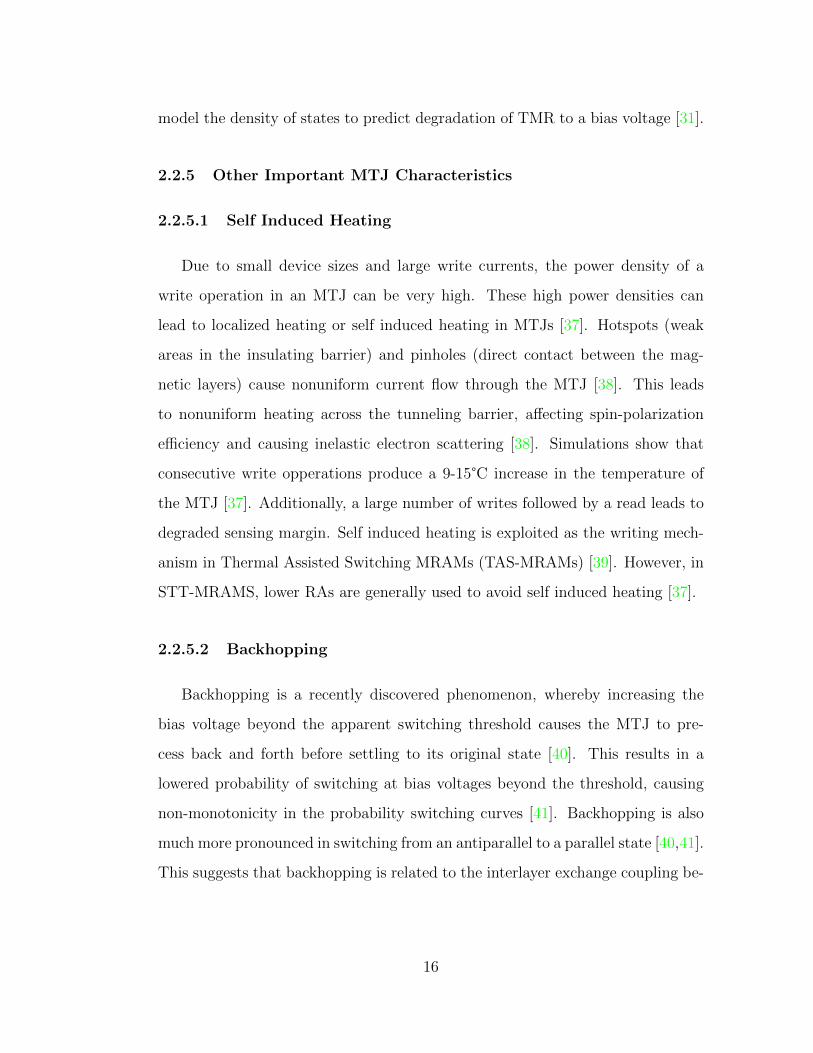
Free Layer
Fixed Layer
Insulator
LW
d
Je
M
P
pm
θ
Figure 3.1: Sketch of basic MTJ structure.
transfer term [2], the normalized LLGE with STT is given by:
∂ ~m
∂t= −γMS ~m×
(~heff +
JeJCb (θ) (~m× ~p)− α∂ ~m
∂t
), (3.1)
where MS = | ~M |, γ is the absolute value of the gyromagnetic ratio (γeµ0), ~m is
the unit vector in the direction of ~M , ~p is the unit vector in the direction of the
magnetization of the fixed layer, ~heff = ~Heff/MS, Je is the current density (see
Fig. 3.1), θ is the angle between ~m and ~p, and α > 0 is the material-dependent
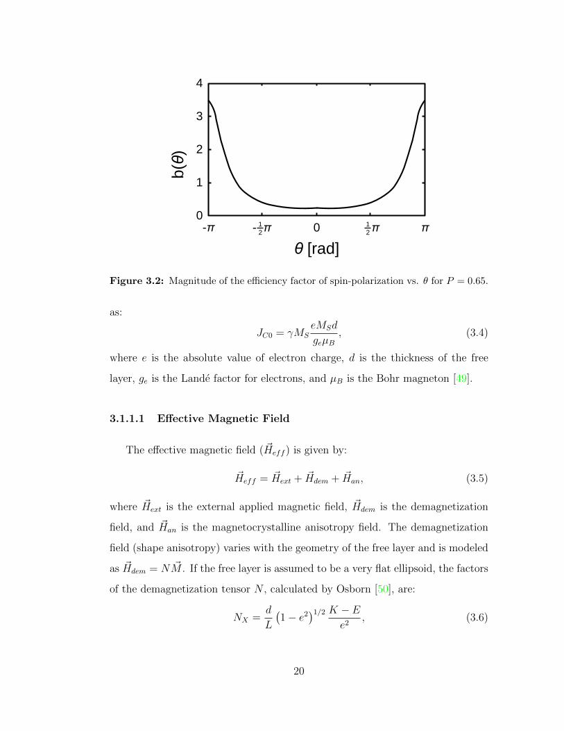
Gilbert damping constant. The efficiency factor of spin-polarization (b (θ), see
Fig. 3.2) is defined as:
b (θ) =
[−4 + (1 + P )3
3 + cos (θ)4P 3/2
]−1, (3.2)
where P is the percentage of electrons polarized in the ~p direction. The switching
current density (JC) has been modified to include thermally-activated switching
[23]. For a constant pulse of duration τ , JC is given by:
JC = JC0
[1− ln (τ/τ0)
∆
], (3.3)
where ∆ is the thermal stability of the MTJ and τ0 = (γMS)−1 is the natural
time constant. Furthermore, the characteristic current density (JC0) is defined
19
-π - π 0 π π0
1
2
3
4
b(θ
)
θ [rad]
1
2
1
2
Figure 3.2: Magnitude of the efficiency factor of spin-polarization vs. θ for P = 0.65.
as:
JC0 = γMSeMSd
geµB, (3.4)
where e is the absolute value of electron charge, d is the thickness of the free
layer, ge is the Lande factor for electrons, and µB is the Bohr magneton [49].
3.1.1.1 Effective Magnetic Field
The effective magnetic field ( ~Heff ) is given by:
~Heff = ~Hext + ~Hdem + ~Han, (3.5)
where ~Hext is the external applied magnetic field, ~Hdem is the demagnetization
field, and ~Han is the magnetocrystalline anisotropy field. The demagnetization
field (shape anisotropy) varies with the geometry of the free layer and is modeled
as ~Hdem = N ~M . If the free layer is assumed to be a very flat ellipsoid, the factors
of the demagnetization tensor N , calculated by Osborn [50], are:
NX =d
L
(1− e2
)1/2 K − Ee2
, (3.6)
20
NY =d
L
K − (1− e2)Ee2 (1− e2)1/2
, (3.7)
NZ = 1− d
L
E
(1− e2)1/2, (3.8)
where K and E are the complete elliptic integrals of the first and second kind
whose argument is:
e =(1−W 2/L2
)1/2. (3.9)
3.1.1.2 Temperature Dependencies
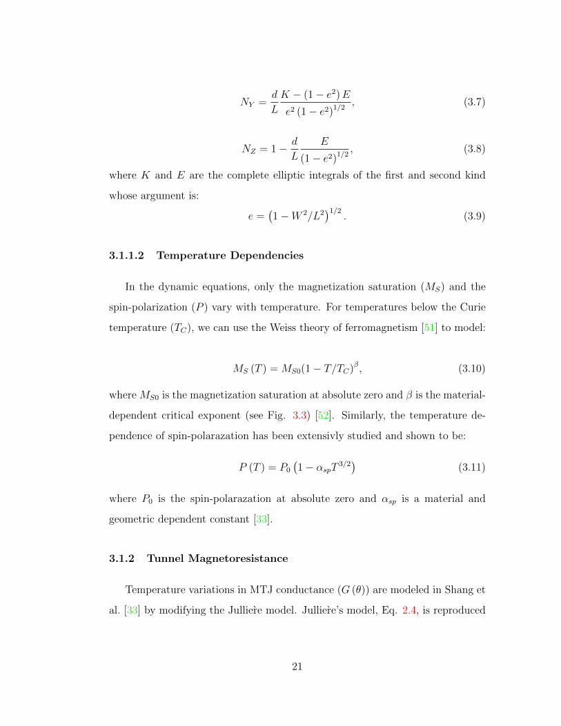
In the dynamic equations, only the magnetization saturation (MS) and the
spin-polarization (P ) vary with temperature. For temperatures below the Curie
temperature (TC), we can use the Weiss theory of ferromagnetism [51] to model:
MS (T ) = MS0(1− T/TC)β, (3.10)
where MS0 is the magnetization saturation at absolute zero and β is the material-
dependent critical exponent (see Fig. 3.3) [52]. Similarly, the temperature de-
pendence of spin-polarazation has been extensivly studied and shown to be:
P (T ) = P0
(1− αspT 3/2
)(3.11)
where P0 is the spin-polarazation at absolute zero and αsp is a material and
geometric dependent constant [33].
3.1.2 Tunnel Magnetoresistance
Temperature variations in MTJ conductance (G (θ)) are modeled in Shang et
al. [33] by modifying the Julliere model. Julliere’s model, Eq. 2.4, is reproduced
21
0 TC
0
0.2
0.4
0.6
0.8
1
MS/M
S0
1
3 TC2
3 TC
Figure 3.3: Normalized plot of magnetization saturation for generic ferromagnetic
materials.
here with P1 = P2 = P :
G (θ) = GT
1 + P 2 cos (θ)
+GSI . (3.12)
As a reminder, the variation of GT due to temperature is negligible, whereas
GSI ∝ T 4/3. Using θ = 0 for parallel magnetization and θ = 180 for anti-
parallel, the tunnel magnetoresistance with zero applied bias voltage (TMR0)
can be expressed as:
TMR0 (T ) =2P 2
0
(1− αspT 3/2
)21− P 2
0 (1− αspT 3/2)2
+ GSI(T )GT (T )
. (3.13)
The Julliere model fails to predict the effects of a bias voltage on TMR [31].
However, this can be rectified with the addition of a simple fitting function:
TMR (T, V ) =TMR0 (T )
1 +(VV0
)2 , (3.14)
where V0 is the voltage at which TMR is halved.
22
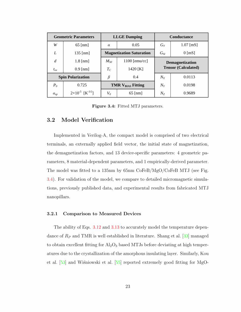
W 65 [nm]
L 135 [nm]
d 1.8 [nm]
Geometric Parameters
tox 0.9 [nm]
MS0 1100 [emu/cc]
TC 1420 [K]
β 0.4
Magnetization Saturation
V0 65 [nm]
TMR VBIAS Fitting
GT 1.07 [mS]
GSI 0 [mS]
Conductance
P0 0.725
αsp 2×10⁻⁵ [K-3/2]
Spin Polarization
α 0.05
LLGE Damping
NX 0.0113
NY 0.0198
Demagnetization
Tensor (Calculated)
NZ 0.9689
Figure 3.4: Fitted MTJ parameters.
3.2 Model Verification
Implemented in Verilog-A, the compact model is comprised of two electrical
terminals, an externally applied field vector, the initial state of magnetization,
the demagnetization factors, and 13 device-specific parameters: 4 geometric pa-
rameters, 8 material-dependent parameters, and 1 empirically-derived parameter.
The model was fitted to a 135nm by 65nm CoFeB/MgO/CoFeB MTJ (see Fig.
3.4). For validation of the model, we compare to detailed micromagnetic simula-
tions, previously published data, and experimental results from fabricated MTJ
nanopillars.
3.2.1 Comparison to Measured Devices
The ability of Eqs. 3.12 and 3.13 to accurately model the temperature depen-
dance of RP and TMR is well established in literature. Shang et al. [33] managed
to obtain excellent fitting for Al2O3 based MTJs before deviating at high temper-
atures due to the crystallization of the amorphous insulating layer. Similarly, Kou
et al. [53] and Wisniowski et al. [55] reported extremely good fitting for MgO-
23
0 100 200 300 400100
200
300
400
500
TM
R [%
]
Temperature [K]
Model
This Work
[53]
[54]
Figure 3.5: TMR vs. temperature: Verliog-A model (line), reported in [53] (triangles),
reported in [54] (squares), and fabricated devices (circles).
-400 -200 0 200 400
100
110
120
130
140
150
160
TM
R [
%]
VBIAS
[mV]
Exp
Mod
Figure 3.6: TMR vs. an applied bias voltage at 300K: Verliog-A model (black line)
and fabricated devices (red circles).
24
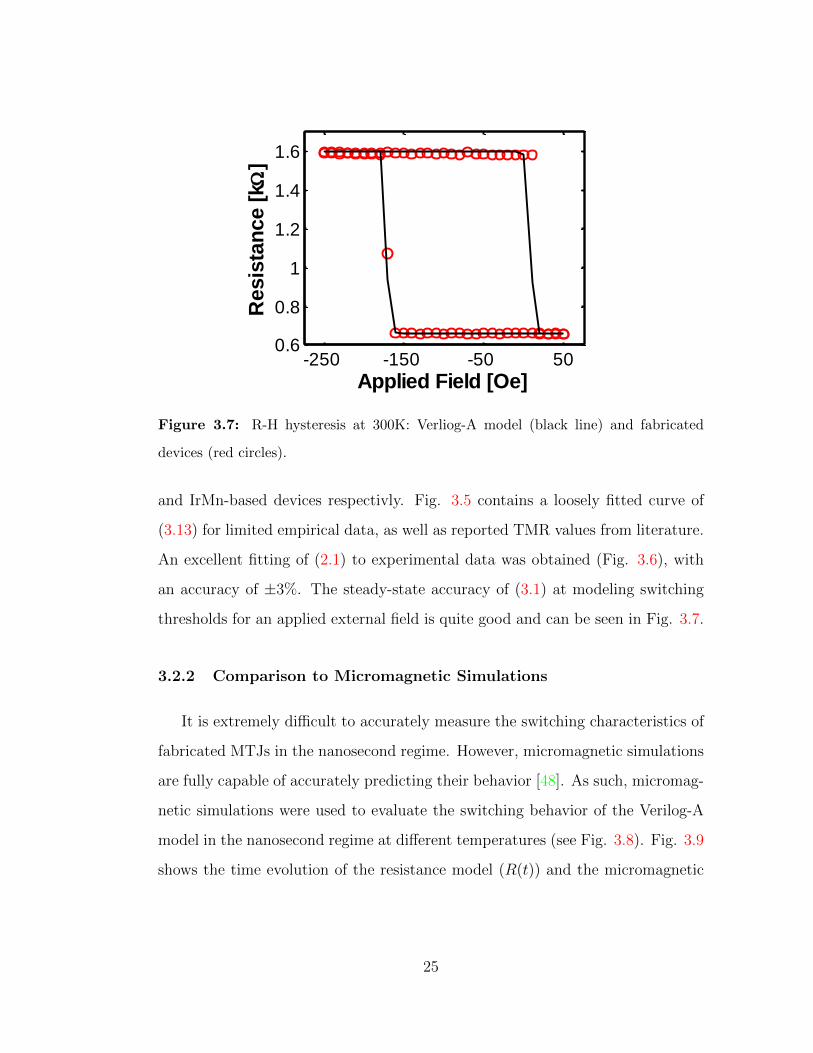
-250 -150 -50 500.6
0.8
1
1.2
1.4
1.6
Resis
tan
ce [
k
]
Applied Field [Oe]
Figure 3.7: R-H hysteresis at 300K: Verliog-A model (black line) and fabricated
devices (red circles).
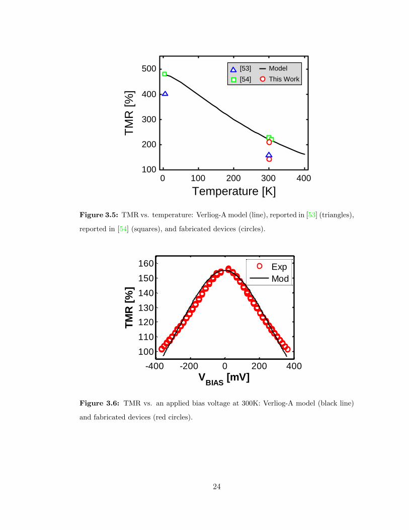
and IrMn-based devices respectivly. Fig. 3.5 contains a loosely fitted curve of
(3.13) for limited empirical data, as well as reported TMR values from literature.
An excellent fitting of (2.1) to experimental data was obtained (Fig. 3.6), with
an accuracy of ±3%. The steady-state accuracy of (3.1) at modeling switching
thresholds for an applied external field is quite good and can be seen in Fig. 3.7.
3.2.2 Comparison to Micromagnetic Simulations
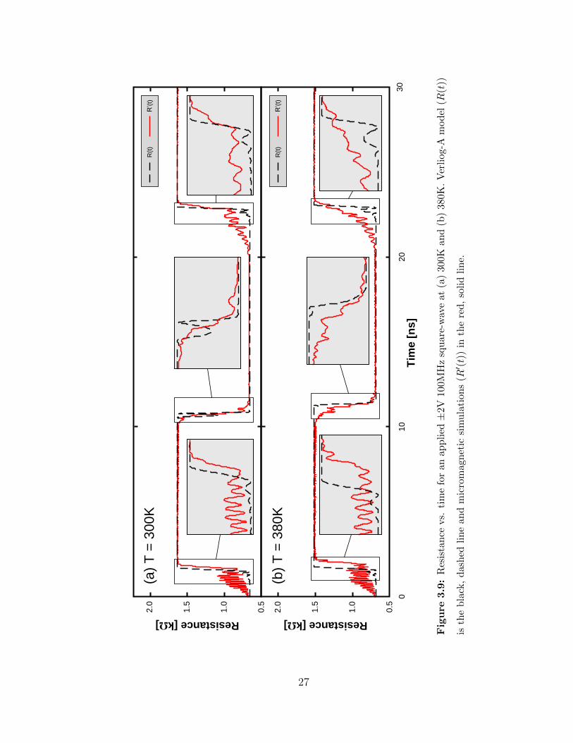
It is extremely difficult to accurately measure the switching characteristics of
fabricated MTJs in the nanosecond regime. However, micromagnetic simulations
are fully capable of accurately predicting their behavior [48]. As such, micromag-
netic simulations were used to evaluate the switching behavior of the Verilog-A
model in the nanosecond regime at different temperatures (see Fig. 3.8). Fig. 3.9
shows the time evolution of the resistance model (R(t)) and the micromagnetic
25
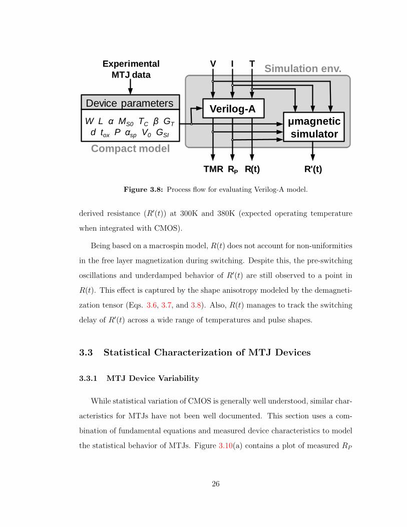
Experimental
MTJ data
Device parametersVerilog-A
μmagnetic
simulator
V I T
TMR RP R(t) R'(t)
Simulation env.
Compact model
W L α MS0 TC β GT
d tox P αsp V0 GSI
Figure 3.8: Process flow for evaluating Verilog-A model.
derived resistance (R′(t)) at 300K and 380K (expected operating temperature
when integrated with CMOS).
Being based on a macrospin model, R(t) does not account for non-uniformities
in the free layer magnetization during switching. Despite this, the pre-switching
oscillations and underdamped behavior of R′(t) are still observed to a point in
R(t). This effect is captured by the shape anisotropy modeled by the demagneti-
zation tensor (Eqs. 3.6, 3.7, and 3.8). Also, R(t) manages to track the switching
delay of R′(t) across a wide range of temperatures and pulse shapes.
3.3 Statistical Characterization of MTJ Devices
3.3.1 MTJ Device Variability
While statistical variation of CMOS is generally well understood, similar char-
acteristics for MTJs have not been well documented. This section uses a com-
bination of fundamental equations and measured device characteristics to model
the statistical behavior of MTJs. Figure 3.10(a) contains a plot of measured RP
26
0.5
1.0
1.5
2.0
Resistance [kΩ]
Tim
e [
ns
]
01
02
03
0
0.5
1.0
1.5
2.0
Resistance [kΩ]
R’(t)
R(t
)
R’(t)
R(t
)
(a)
T =
30
0K
(b)
T =
38
0K
Figure
3.9:
Res
ista
nce
vs.
tim
efo
ran
app
lied±
2V10
0MH
zsq
uar
e-w
ave
at(a
)30
0Kan
d(b
)38
0K.
Ver
liog
-Am
od
el(R
(t))
isth
eb
lack
,d
ash
edlin
ean
dm
icro
magn
etic
sim
ula
tion
s(R′ (t)
)in
the
red
,so
lid
lin
e.
27
(a) (b)
X
YZ
2
1.5
10.5 1 1.5
RP [kΩ]
RA
P [kΩ
]
2.5
X Y Z
120
110
100
90
80
TM
R [%
]
RA [Ω∙μm2]
4 4.5 5 5.5 6
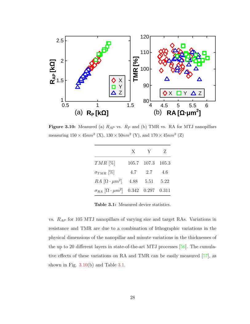
Figure 3.10: Measured (a) RAP vs. RP and (b) TMR vs. RA for MTJ nanopillars
measuring 150× 45nm2 (X), 130× 50nm2 (Y), and 170× 45nm2 (Z)
X Y Z
TMR [%] 105.7 107.3 105.3
σTMR [%] 4.7 2.7 4.6
RA [Ω · µm2] 4.88 5.51 5.22
σRA [Ω · µm2] 0.342 0.297 0.311
Table 3.1: Measured device statistics.
vs. RAP for 105 MTJ nanopillars of varying size and target RAs. Variations in
resistance and TMR are due to a combination of lithographic variations in the
physical dimensions of the nanopillar and minute variations in the thicknesses of
the up to 20 different layers in state-of-the-art MTJ processes [56]. The cumula-
tive effects of these variations on RA and TMR can be easily measured [57], as
shown in Fig. 3.10(b) and Table 3.1.
28
wl
d
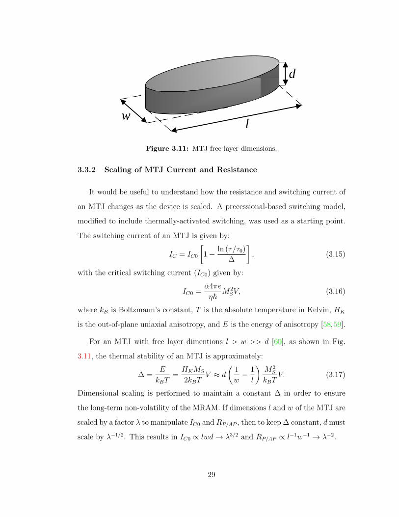
Figure 3.11: MTJ free layer dimensions.
3.3.2 Scaling of MTJ Current and Resistance
It would be useful to understand how the resistance and switching current of
an MTJ changes as the device is scaled. A precessional-based switching model,
modified to include thermally-activated switching, was used as a starting point.
The switching current of an MTJ is given by:
IC = IC0
[1− ln (τ/τ0)
∆
], (3.15)
with the critical switching current (IC0) given by:
IC0 =α4πe
η~M2
SV, (3.16)
where kB is Boltzmann’s constant, T is the absolute temperature in Kelvin, HK
is the out-of-plane uniaxial anisotropy, and E is the energy of anisotropy [58,59].
For an MTJ with free layer dimentions l > w >> d [60], as shown in Fig.
3.11, the thermal stability of an MTJ is approximately:
∆ =E
kBT=HKMS
2kBTV ≈ d
(1
w− 1
l
)M2
S
kBTV. (3.17)
Dimensional scaling is performed to maintain a constant ∆ in order to ensure
the long-term non-volatility of the MRAM. If dimensions l and w of the MTJ are
scaled by a factor λ to manipulate IC0 and RP/AP , then to keep ∆ constant, dmust
scale by λ−1/2. This results in IC0 ∝ lwd→ λ3/2 and RP/AP ∝ l−1w−1 → λ−2.
29
CHAPTER 4
Memory Architectures
Several different types of memory architectures exist for STT-MRAMs. At
the cell level, many architectures are tailored to certain MTJ characteristics,
more specifically to the ratio of the critical writing currents IC(P → AP ) and
IC(AP → P ). Other cell architectures attempt to exploit the different thresholds
between reading and writing current to increase effective memory density. At the
array level, several different subarraying techniques are employed to maximize
performance and minimize area.
4.1 Cell Architectures
4.1.1 1T-1MTJ
There are two widely used 1T-1MTJ STT-MRAM cell architectures, the “con-
ventional” cell (Fig. 4.1(a)) and the “reverse” cell (Fig. 4.1(b)) [61]. The “con-
ventional” architecture gets its name from that fact that most MTJ are deposited
with the fixed layer on the bottom. A smooth deposition surface is required to
form a high quality pinning layer capable of generating the fixed layer [62]. The
surface roughness introduced by various film deposition steps generally makes de-
positing the pinning layer on the top of the MTJ stack impractical. This means
that it is easier to connect the fixed layer of the MTJ to the access transistor and
30
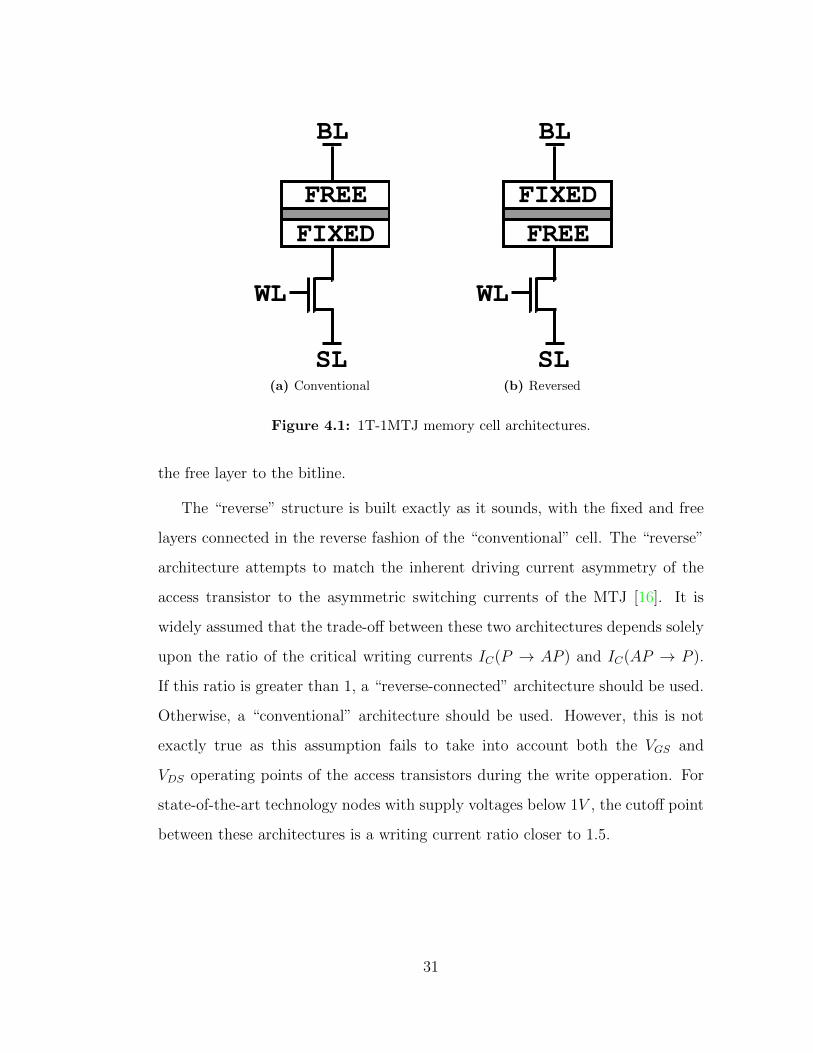
FREE
FIXED
WL
BL
SL(a) Conventional
WL
BL
SL
FIXED
FREE
(b) Reversed
Figure 4.1: 1T-1MTJ memory cell architectures.
the free layer to the bitline.
The “reverse” structure is built exactly as it sounds, with the fixed and free
layers connected in the reverse fashion of the “conventional” cell. The “reverse”
architecture attempts to match the inherent driving current asymmetry of the
access transistor to the asymmetric switching currents of the MTJ [16]. It is
widely assumed that the trade-off between these two architectures depends solely
upon the ratio of the critical writing currents IC(P → AP ) and IC(AP → P ).
If this ratio is greater than 1, a “reverse-connected” architecture should be used.
Otherwise, a “conventional” architecture should be used. However, this is not
exactly true as this assumption fails to take into account both the VGS and
VDS operating points of the access transistors during the write opperation. For
state-of-the-art technology nodes with supply voltages below 1V , the cutoff point
between these architectures is a writing current ratio closer to 1.5.
31
MTJ1
SL BL<1>
MTJ2
MTJM
WL
BL<2> BL<M>
Figure 4.2: Shared memory cell architecture with M MTJs per transistor.
4.1.2 Shared
Access device “sharing” is one potential technique for increasing cell density.
As shown in Fig. 4.2, one access transistor is connected to multiple MTJ devices,
with additional bitlines to support independant access. This also allows the access
transistor to be sized up to provide higher write current while maintaining the
same overall memory density. However, there are several shortcomings associated
with this technique which will be discussed in future sections.
4.1.3 Stacked
MTJ device “stacking” is another potential technique to increase cell density.
“Stacking” works by connecting several different types of MTJ in series with one
access transistor, shown in Fig. 4.3, in a similar fashion to multi-bit Flash cells.
32
MTJ1
SLMTJN
WL BL
Figure 4.3: Stacked memory cell architecture with N MTJs per transistor.
To ensure functionality, the resistance and critical writing current of each MTJ
need to be sufficiently different. Reading and writing to a cell would require
multiple cycles, one for each bit.
4.2 Subarraying
4.2.1 1T-1MTJ
As stated before, subarraying is necessary for larger memories. Single, large
memory arrays are slow and require additional buffering to drive very long wires.
Breaking it up into several smaller subarrays allows the memory to operate faster
and share peripheral circuitry. For 1T-1MTJ cell architectures, the number of
cells per bitline is limited by the capacitance of the access transistor and the MTJ
itself. Generally, a single bitline can support no more than 256 cells.
4.2.2 Shared Architectures
As mentioned earlier, there are several shortcomings to a “shared” MTJ ar-
chitecture. During the write operation, there are multiple parasitic current paths
that siphon current from the device being written to, forcing the access device to
be sized up. These parasitic currents also have the potential to flip cells not being
33
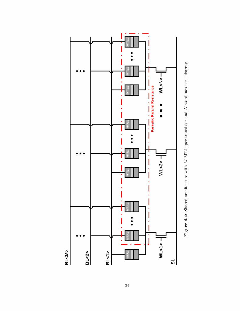
SL
BL
<1
>
WL
<1
>
BL
<2
>
BL
<M
>
WL
<2
>W
L<
N>
MT
J1
,1M
TJ
1,2
MT
J1
,MM
TJ
2,1
MT
J2
,2M
TJ
2,M
MT
JN
,1M
TJ
N,2
MT
JN
,M
Pa
ras
itic
Pa
ralle
l R
es
ista
nc
e
Figure
4.4:
Sh
are
darc
hit
ectu
rew
ithM
MT
Js
per
tran
sist
oran
dN
wor
dli
nes
per
subar
ray.
34
accessed. When reading, these parasitic paths lower the effective TMR that can
be observed.
For M MTJs per access device and N wordlines per subarray, the effective
TMR (TMReff ) can be expressed as:
TMReff =2 (N +M − 1)−NM
NM + (N − 1) (M − 1) · TMR· TMR. (4.1)
The worst case TMR degradation can be easily derived by finding the largest pos-
sible RP and the smallest possible RAP . If R‖ is the parasitic parallel resistance
shown in Fig. 4.4, then RP,MAX can be calculated as RP ‖ R‖, where:
R‖ =N +M − 1
(N − 1) (M − 1)· (1 + TMR) ·RP (4.2)
for the case of all parasitic resistances in the antiparallel state. Similarly, RAP,MIN
can be calculated as RP · (1 + TMR) ‖ R‖, where:
R‖ =N +M − 1
(N − 1) (M − 1)·RP (4.3)
for the case of all parasitic resistances in the parallel state. For M > 2, TMReff
is negative, limiting sharing to only two MTJs per access device.
In order to quantify the impact of sharing on the writing operation, the max-
imum allowable disturbance current a parasitic device can handle before a signif-
icant probability of switching occurs must first be calculated. For M = 2, since
the ability to read is already limited, the four worst corner cases are shown in
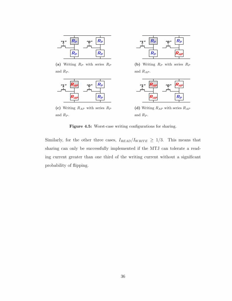
Fig. 4.5. For the corner case of Fig. 4.5(a), we require:
RP ·IWRITE (P → AP )−RP ·IREAD (P → AP ) ≤ 2RP ·IREAD (P → AP ) . (4.4)
Solving:IREAD (P → AP )
IWRITE (P → AP )≥ 1
3. (4.5)
35
RP“1”
RP
RP“0”
RP
(a) Writing RP with series RP
and RP .
RP“1”
RP
RP“0”
RAP
(b) Writing RP with series RP
and RAP .
RAP“1”
RAP
RP“0”
RP
(c) Writing RAP with series RP
and RP .
RAP“1”
RAP
RAP“0”
RP
(d) Writing RAP with series RAP
and RP .
Figure 4.5: Worst-case writing configurations for sharing.
Similarly, for the other three cases, IREAD/IWRITE ≥ 1/3. This means that
sharing can only be successfully implemented if the MTJ can tolerate a read-
ing current greater than one third of the writing current without a significant
probability of flipping.
36
CHAPTER 5
Design-Space Analysis
In order to design an STT-MRAM with adequate design margin for high
yield, one must consider all the implications of MTJ/CMOS integration. The
design depends considerably on the underlying transistor technology, since a given
CMOS technology constrains the design space due to the overhead and impact of
the access transistor in each memory cell. The feasibility and yield of the memory
are also heavily dependent upon the variation of the MTJs [63]. Previous work,
such as Raychowdhury et al. [64], has failed to address these dependencies and
provide the necessary framework for large-scale design. This chapter introduces
the concept of the memory cell design space and a sensitivity analysis to optimize
yield, power, and density for an STT-MRAM.
5.1 Defining the Design Space
The analysis in this chapter is done for a conventional 1T-1MTJ cell architec-
ture as shown in Fig. 5.1, but can be generalized to any cell architecture. The
writing currents for flipping the cell resistance are defined as IC(P → AP ) and
IC(AP → P ). The design space of a single STT-MRAM memory cell can be
illustrated using an RAP vs. RP plot as is shown in Fig. 5.2. The feasibility
region is indicated by the shaded region. It contains all points (RP , RAP ) in the
design space so that a memory cell made with such an MTJ is functional. In the
37
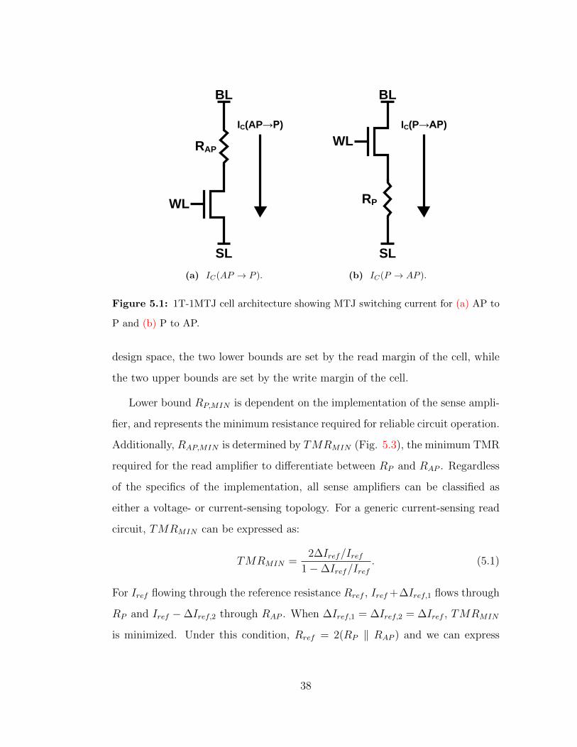
RAP
WL
BL
IC(AP→P)
SL
(a) IC(AP → P ).
RP
WL
BL
IC(P→AP)
SL
(b) IC(P → AP ).
Figure 5.1: 1T-1MTJ cell architecture showing MTJ switching current for (a) AP to
P and (b) P to AP.
design space, the two lower bounds are set by the read margin of the cell, while
the two upper bounds are set by the write margin of the cell.
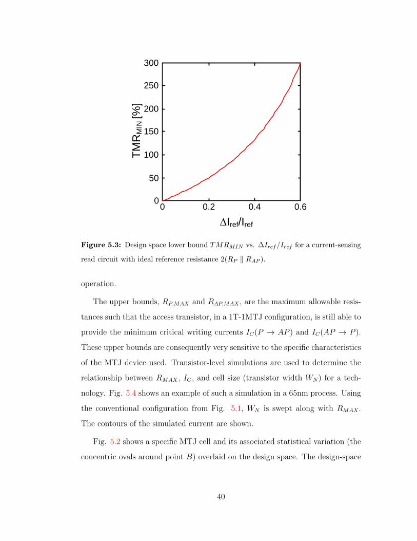
Lower bound RP,MIN is dependent on the implementation of the sense ampli-
fier, and represents the minimum resistance required for reliable circuit operation.
Additionally, RAP,MIN is determined by TMRMIN (Fig. 5.3), the minimum TMR
required for the read amplifier to differentiate between RP and RAP . Regardless
of the specifics of the implementation, all sense amplifiers can be classified as
either a voltage- or current-sensing topology. For a generic current-sensing read
circuit, TMRMIN can be expressed as:
TMRMIN =2∆Iref/Iref
1−∆Iref/Iref. (5.1)
For Iref flowing through the reference resistance Rref , Iref +∆Iref,1 flows through
RP and Iref −∆Iref,2 through RAP . When ∆Iref,1 = ∆Iref,2 = ∆Iref , TMRMIN
is minimized. Under this condition, Rref = 2(RP ‖ RAP ) and we can express
38
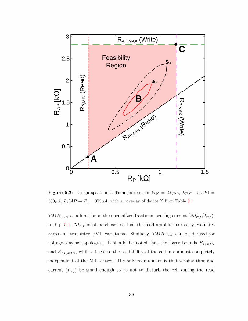
0 0.5 1 1.50
0.5
1
1.5
2
2.5
3
A
C
B
5
3
RA
P [kΩ
]
RP [kΩ]
RP
,MIN
(R
ea
d)
RAP,MIN (R
ead)
RP
,MA
X (Write
)
RAP,MAX (Write)
Feasibility
Region
Figure 5.2: Design space, in a 65nm process, for WN = 2.0µm, IC(P → AP ) =
500µA, IC(AP → P ) = 375µA, with an overlay of device X from Table 3.1.
TMRMIN as a function of the normalized fractional sensing current (∆Iref/Iref ).
In Eq. 5.1, ∆Iref must be chosen so that the read amplifier correctly evaluates
across all transistor PVT variations. Similarly, TMRMIN can be derived for
voltage-sensing topologies. It should be noted that the lower bounds RP,MIN
and RAP,MIN , while critical to the readability of the cell, are almost completely
independent of the MTJs used. The only requirement is that sensing time and
current (Iref ) be small enough so as not to disturb the cell during the read
39
0 0.2 0.4 0.60
50
100
150
200
250
300
TM
RM
IN [%
]
Iref/Iref
Figure 5.3: Design space lower bound TMRMIN vs. ∆Iref/Iref for a current-sensing
read circuit with ideal reference resistance 2(RP ‖ RAP ).
operation.
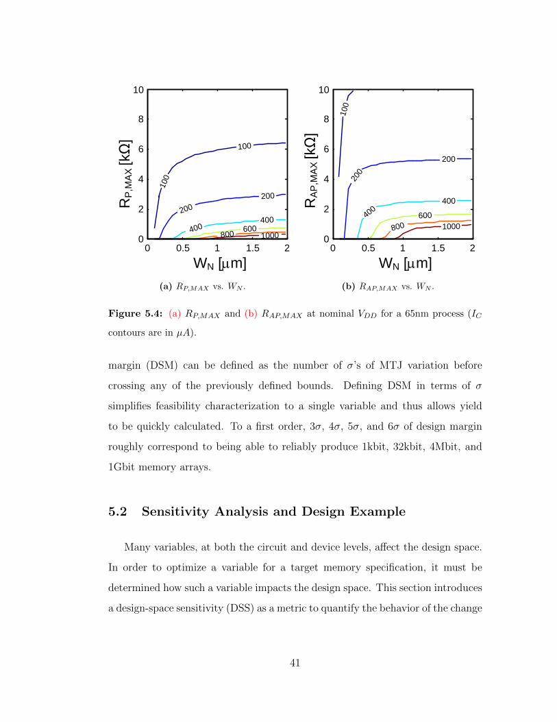
The upper bounds, RP,MAX and RAP,MAX , are the maximum allowable resis-
tances such that the access transistor, in a 1T-1MTJ configuration, is still able to
provide the minimum critical writing currents IC(P → AP ) and IC(AP → P ).
These upper bounds are consequently very sensitive to the specific characteristics
of the MTJ device used. Transistor-level simulations are used to determine the
relationship between RMAX , IC , and cell size (transistor width WN) for a tech-
nology. Fig. 5.4 shows an example of such a simulation in a 65nm process. Using
the conventional configuration from Fig. 5.1, WN is swept along with RMAX .
The contours of the simulated current are shown.
Fig. 5.2 shows a specific MTJ cell and its associated statistical variation (the
concentric ovals around point B) overlaid on the design space. The design-space
40
1000800600
400
400
200
200
100
100
0 0.5 1 1.5 20
2
4
6
8
10
WN [m]
RP
,MA
X [kΩ
]
(a) RP,MAX vs. WN .
1000800
600400400
200
200
100
0 0.5 1 1.5 20
2
4
6
8
10
WN [m]
RA
P,M
AX
[kΩ
]
(b) RAP,MAX vs. WN .
Figure 5.4: (a) RP,MAX and (b) RAP,MAX at nominal VDD for a 65nm process (IC
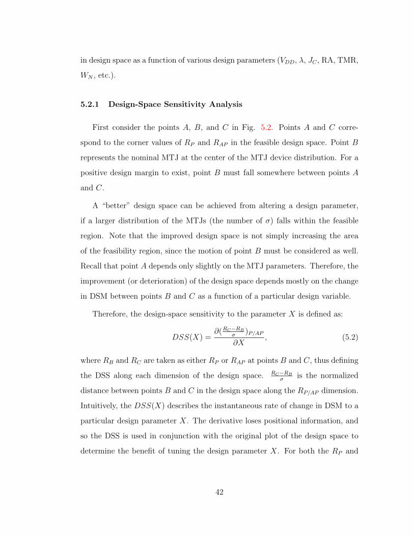
contours are in µA).
margin (DSM) can be defined as the number of σ’s of MTJ variation before
crossing any of the previously defined bounds. Defining DSM in terms of σ
simplifies feasibility characterization to a single variable and thus allows yield
to be quickly calculated. To a first order, 3σ, 4σ, 5σ, and 6σ of design margin
roughly correspond to being able to reliably produce 1kbit, 32kbit, 4Mbit, and
1Gbit memory arrays.
5.2 Sensitivity Analysis and Design Example
Many variables, at both the circuit and device levels, affect the design space.
In order to optimize a variable for a target memory specification, it must be
determined how such a variable impacts the design space. This section introduces
a design-space sensitivity (DSS) as a metric to quantify the behavior of the change
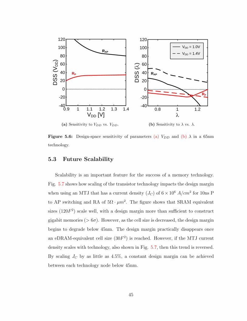
41
in design space as a function of various design parameters (VDD, λ, JC , RA, TMR,
WN , etc.).
5.2.1 Design-Space Sensitivity Analysis
First consider the points A, B, and C in Fig. 5.2. Points A and C corre-
spond to the corner values of RP and RAP in the feasible design space. Point B
represents the nominal MTJ at the center of the MTJ device distribution. For a
positive design margin to exist, point B must fall somewhere between points A
and C.
A “better” design space can be achieved from altering a design parameter,
if a larger distribution of the MTJs (the number of σ) falls within the feasible
region. Note that the improved design space is not simply increasing the area
of the feasibility region, since the motion of point B must be considered as well.
Recall that point A depends only slightly on the MTJ parameters. Therefore, the
improvement (or deterioration) of the design space depends mostly on the change
in DSM between points B and C as a function of a particular design variable.
Therefore, the design-space sensitivity to the parameter X is defined as:
DSS(X) =∂(RC−RB
σ)P/AP
∂X, (5.2)
where RB and RC are taken as either RP or RAP at points B and C, thus defining
the DSS along each dimension of the design space. RC−RB
σis the normalized
distance between points B and C in the design space along the RP/AP dimension.
Intuitively, the DSS(X) describes the instantaneous rate of change in DSM to a
particular design parameter X. The derivative loses positional information, and
so the DSS is used in conjunction with the original plot of the design space to
determine the benefit of tuning the design parameter X. For both the RP and
42

RAP dimensions, if DSS(X) > 0, then the DSM is improved by increasing X,
and if DSS(X) < 0, then DSM is improved by decreasing X. When the design-
space sensitivities for the two dimensions conflict, the size of the design space in
each dimension should then be taken into account.
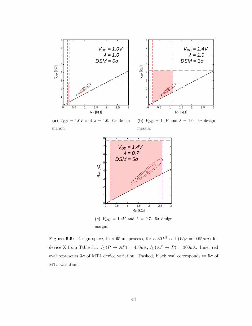
5.2.2 Design Example
In this section, the sensitivity analysis was used to design a 4Mbit STT-
MRAM with a 30F 2 cell size (comparable to eDRAM) in a 65nm technology.
Device X from Table 3.1, with IC(P → AP ) = 450µA and IC(AP → P ) =
300µA, is the nominal MTJ and can be scaled by λ. Also, approximately 5σ of
design margin is required for reasonable yield.
Fig. 5.5(a) shows the design space for a nominal VDD = 1.0V and λ = 1.0.
The inner red oval is the 3σ variation of the MTJ, while the dashed, black oval
represents the 5σ variation of the MTJ. Clearly, with nominal VDD and λ, the
memory is not functional. Fig. 5.6 shows that the design space is much more
sensitive to VDD than it is to λ. Therefore, we choose to scale VDD to 1.4V . Fig.
5.5(b) shows the new design space, with the 3σ bound at the edge of the design
boundary.
Scaling VDD alone proves insufficient to meet the 5σ design margin required,
and so λ was simultaneously scaled. Fig. 5.6(b) shows that scaling λ results in
conflicting DSS. The RAP margin improves more by scaling λ up, while the RP
margin improves by scaling λ down. However, Fig. 5.5(b) indicates that RAP
has considerable margin, and we can trade off some of that margin for improved
margin in RP . Therefore, we choose to scale λ down to 0.7. As we can see in Fig.
5.5(c), the desired 5σ bound on MTJ variation is essentially enclosed within the
design space.
43
0 0.5 1 1.5 2 2.5 30
1
2
3
4
5
6
7
8
RA
P [
k
]
RP [k]
VDD = 1.0V
λ = 1.0
DSM = 0σ
(a) VDD = 1.0V and λ = 1.0. 0σ design
margin.
0 0.5 1 1.5 2 2.5 30
1
2
3
4
5
6
7
8
RA
P [
k
]
RP [k]
VDD = 1.4V
λ = 1.0
DSM = 3σ
(b) VDD = 1.4V and λ = 1.0. 3σ design
margin.
0 0.5 1 1.5 2 2.5 30
1
2
3
4
5
6
7
8
RA
P [
k
]
RP [k]
VDD = 1.4V
λ = 0.7
DSM = 5σ
(c) VDD = 1.4V and λ = 0.7. 5σ design
margin.
Figure 5.5: Design space, in a 65nm process, for a 30F 2 cell (WN = 0.65µm) for
device X from Table 3.1: IC(P → AP ) = 450µA, IC(AP → P ) = 300µA. Inner red
oval represents 3σ of MTJ device variation. Dashed, black oval corresponds to 5σ of
MTJ variation.
44
0.9 1 1.1 1.2 1.3-40
-20
0
20
40
60
80
100
120
1.4
DS
S (
VD
D)
VDD [V]
RP
RAP
(a) Sensitivity to VDD vs. VDD.
0.8 1 1.2-40
-20
0
20
40
60
80
100
120
DS
S ()
RP
RAP
VDD = 1.0V
VDD = 1.4V
(b) Sensitivity to λ vs. λ.
Figure 5.6: Design-space sensitivity of parameters (a) VDD and (b) λ in a 65nm
technology.
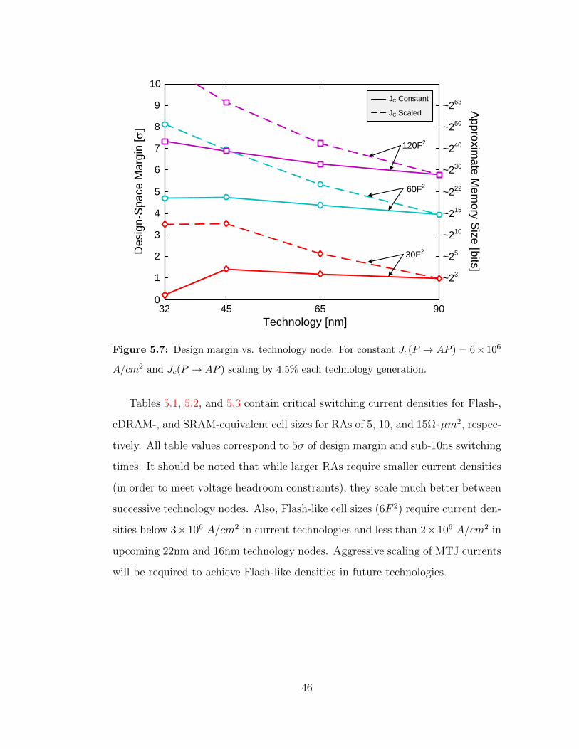
5.3 Future Scalability
Scalability is an important feature for the success of a memory technology.
Fig. 5.7 shows how scaling of the transistor technology impacts the design margin
when using an MTJ that has a current density (JC) of 6× 10⁶ A/cm2 for 10ns P
to AP switching and RA of 5Ω · µm2. The figure shows that SRAM equivalent
sizes (120F 2) scale well, with a design margin more than sufficient to construct
gigabit memories (> 6σ). However, as the cell size is decreased, the design margin
begins to degrade below 45nm. The design margin practically disappears once
an eDRAM-equivalent cell size (30F 2) is reached. However, if the MTJ current
density scales with technology, also shown in Fig. 5.7, then this trend is reversed.
By scaling JC by as little as 4.5%, a constant design margin can be achieved
between each technology node below 45nm.
45
De
sig
n-S
pa
ce
Ma
rgin
[]
32 45 65 900
1
2
3
4
5
6
7
8
9
10
Technology [nm]
120F2
60F2
30F2
JC Constant
JC Scaled
~23
~25
~210
~215
~222
~230
~240
~250
~263
Ap
pro
xim
ate
Me
mo
ry S
ize
[bits
]
Figure 5.7: Design margin vs. technology node. For constant Jc(P → AP ) = 6× 10⁶
A/cm2 and Jc(P → AP ) scaling by 4.5% each technology generation.
Tables 5.1, 5.2, and 5.3 contain critical switching current densities for Flash-,
eDRAM-, and SRAM-equivalent cell sizes for RAs of 5, 10, and 15Ω·µm2, respec-
tively. All table values correspond to 5σ of design margin and sub-10ns switching
times. It should be noted that while larger RAs require smaller current densities
(in order to meet voltage headroom constraints), they scale much better between
successive technology nodes. Also, Flash-like cell sizes (6F 2) require current den-
sities below 3×10⁶ A/cm2 in current technologies and less than 2×10⁶ A/cm2 in
upcoming 22nm and 16nm technology nodes. Aggressive scaling of MTJ currents
will be required to achieve Flash-like densities in future technologies.
46
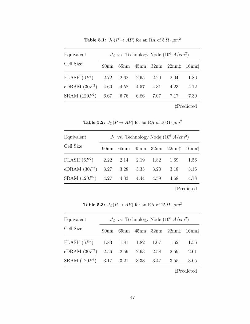
Table 5.1: JC(P → AP ) for an RA of 5 Ω · µm2
Equivalent
Cell Size
JC vs. Technology Node (106 A/cm2)
90nm 65nm 45nm 32nm 22nm‡ 16nm‡
FLASH (6F 2) 2.72 2.62 2.65 2.20 2.04 1.86
eDRAM (30F 2) 4.60 4.58 4.57 4.31 4.23 4.12
SRAM (120F 2) 6.67 6.76 6.86 7.07 7.17 7.30
‡Predicted
Table 5.2: JC(P → AP ) for an RA of 10 Ω · µm2
Equivalent
Cell Size
JC vs. Technology Node (106 A/cm2)
90nm 65nm 45nm 32nm 22nm‡ 16nm‡
FLASH (6F 2) 2.22 2.14 2.19 1.82 1.69 1.56
eDRAM (30F 2) 3.27 3.28 3.33 3.20 3.18 3.16
SRAM (120F 2) 4.27 4.33 4.44 4.59 4.68 4.78
‡Predicted
Table 5.3: JC(P → AP ) for an RA of 15 Ω · µm2
Equivalent
Cell Size
JC vs. Technology Node (106 A/cm2)
90nm 65nm 45nm 32nm 22nm‡ 16nm‡
FLASH (6F 2) 1.83 1.81 1.82 1.67 1.62 1.56
eDRAM (30F 2) 2.56 2.59 2.63 2.58 2.59 2.61
SRAM (120F 2) 3.17 3.21 3.33 3.47 3.55 3.65
‡Predicted
47
CHAPTER 6
Memory Design
In this chapter, the design flow of three test chips implemented in 90nm,
65nm, and 45nm processes is described. Several architectures from Chapter 4
were selected for testing. Each design was subjected to the analysis outlined in
Chapter 5 in order to optimize read/write performance, memory density, and
energy considerations. Each chip was designed to operate with MTJs fabricated
by UCLA’s Western Institute of Nanoelectronics (WIN). MTJ device specifica-
tions are detailed in [65], [66] and [67]. However, manufacturing requirements
and restrictions made integration of MTJs with CMOS not possible on the test
chips. A brief explanation is provided with a discussion of the process flow for
MTJ/CMOS integration before the chip design is described.
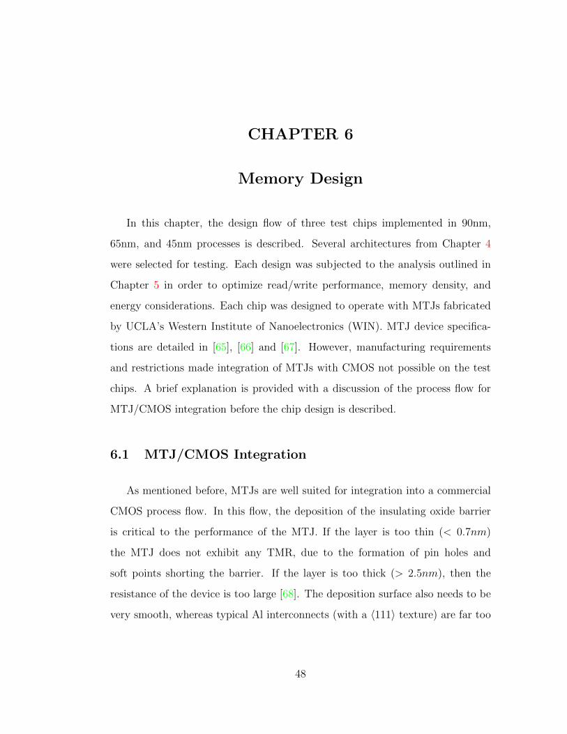
6.1 MTJ/CMOS Integration
As mentioned before, MTJs are well suited for integration into a commercial
CMOS process flow. In this flow, the deposition of the insulating oxide barrier
is critical to the performance of the MTJ. If the layer is too thin (< 0.7nm)
the MTJ does not exhibit any TMR, due to the formation of pin holes and
soft points shorting the barrier. If the layer is too thick (> 2.5nm), then the
resistance of the device is too large [68]. The deposition surface also needs to be
very smooth, whereas typical Al interconnects (with a 〈111〉 texture) are far too
48
Poly
n+ n+
M1
M2SL
WL M3
M4
MTJ
M5 BL
To Sense Amp
Figure 6.1: MTJ/CMOS integration at M4.
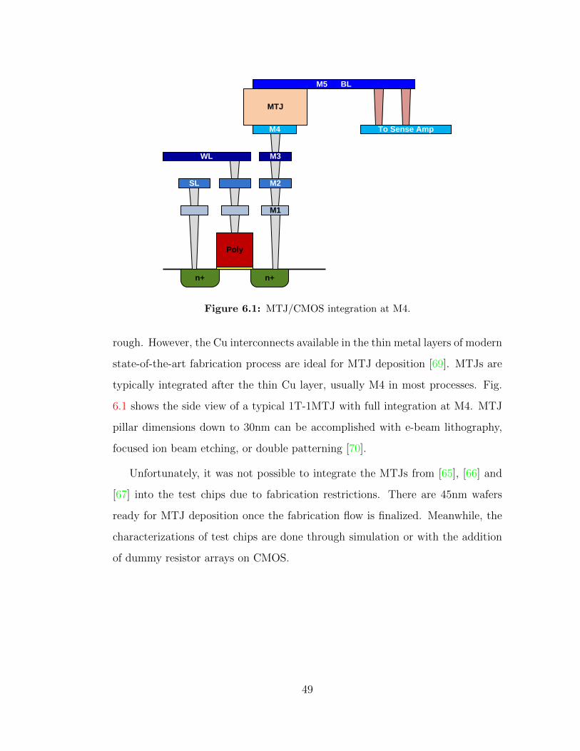
rough. However, the Cu interconnects available in the thin metal layers of modern
state-of-the-art fabrication process are ideal for MTJ deposition [69]. MTJs are
typically integrated after the thin Cu layer, usually M4 in most processes. Fig.
6.1 shows the side view of a typical 1T-1MTJ with full integration at M4. MTJ
pillar dimensions down to 30nm can be accomplished with e-beam lithography,
focused ion beam etching, or double patterning [70].
Unfortunately, it was not possible to integrate the MTJs from [65], [66] and
[67] into the test chips due to fabrication restrictions. There are 45nm wafers
ready for MTJ deposition once the fabrication flow is finalized. Meanwhile, the
characterizations of test chips are done through simulation or with the addition
of dummy resistor arrays on CMOS.
49
6.2 Test Chips
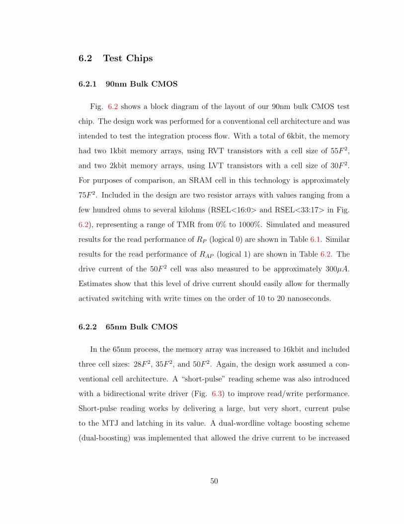
6.2.1 90nm Bulk CMOS
Fig. 6.2 shows a block diagram of the layout of our 90nm bulk CMOS test
chip. The design work was performed for a conventional cell architecture and was
intended to test the integration process flow. With a total of 6kbit, the memory
had two 1kbit memory arrays, using RVT transistors with a cell size of 55F 2,
and two 2kbit memory arrays, using LVT transistors with a cell size of 30F 2.
For purposes of comparison, an SRAM cell in this technology is approximately
75F 2. Included in the design are two resistor arrays with values ranging from a
few hundred ohms to several kilohms (RSEL<16:0> and RSEL<33:17> in Fig.
6.2), representing a range of TMR from 0% to 1000%. Simulated and measured
results for the read performance of RP (logical 0) are shown in Table 6.1. Similar
results for the read performance of RAP (logical 1) are shown in Table 6.2. The
drive current of the 50F 2 cell was also measured to be approximately 300µA.
Estimates show that this level of drive current should easily allow for thermally
activated switching with write times on the order of 10 to 20 nanoseconds.
6.2.2 65nm Bulk CMOS
In the 65nm process, the memory array was increased to 16kbit and included
three cell sizes: 28F 2, 35F 2, and 50F 2. Again, the design work assumed a con-
ventional cell architecture. A “short-pulse” reading scheme was also introduced
with a bidirectional write driver (Fig. 6.3) to improve read/write performance.
Short-pulse reading works by delivering a large, but very short, current pulse
to the MTJ and latching in its value. A dual-wordline voltage boosting scheme
(dual-boosting) was implemented that allowed the drive current to be increased
50
STD
Array
(1K)
LVT
Array
(2K)
STD
Array
(1K)
LVT
Array
(2K)
Row
Decoder
Row
Decoder
COL MUX
COL MUX
Sense Amp
& I/O Buffer
COL MUX
COL MUX
Sense Amp
& I/O BufferRo
w
Pre
-De
co
de
r
CO
L
De
co
de
r
BL
_L<
7>
BL
_L<
6>
BL
_L<
0>
BL
_R
<7
>
BL
_R
<6
>
BL
_R
<0
>
BL
_M
<1>
BL
_M
<0>
BL
_L<
15>
BL
_L<
14>
BL
_L<
00>
BL
_R
<1
5>
BL
_R
<1
4>
BL
_R
<0
0>
BL
_M
<1>
BL
_M
<0>
BL
_L<
7>
BL
_L<
6>
BL
_L<
0>
BL
_R
<7
>
BL
_R
<6
>
BL
_R
<0
>
BL
_M
<1>
BL
_M
<0>
BL
_L<
15>
BL
_L<
14>
BL
_L<
00>
BL
_R
<1
5>
BL
_R
<1
4>
BL
_R
<0
0>
BL
_M
<1>
BL
_M
<0>
CSEL_T<3:0>
CSEL_B<3:0>
EN_T_EV
EN_T_OD
EN_B_EV
EN_B_OD
MB
L_
L
MB
L_
R
RBL_L RBL_R
MB
L_
L
MB
L_
R
RBL_L RBL_R
MB
L_
L
MB
L_
R
RBL_L RBL_R MB
L_
L
MB
L_
R
RBL_L RBL_R
WL_T<63>
WL_T<62>
WL_T<61>
WL_T<02>
WL_T<01>
WL_T<00>
WL_B<63>
WL_B<62>
WL_B<61>
WL_B<02>
WL_B<01>
WL_B<00>
D<1:0>
Q<1:0>
D<3:2>
Q<3:2>
A<2:0>A<8:3> A<9>
COL
RES
COL
RES
PROG
RES
COL
RES
COL
RES
PROG
RES
R_
L<
7>
R_
L<
0>
R_
R<
7>
R_
R<
0>
R_
M
R_
L<
7>
R_
L<
0>
R_
R<
7>
R_
R<
0>
R_
M
COL
RES
COL
RES
PROG
RES
COL
RES
COL
RES
PROG
RES
R_
L<
7>
R_
L<
0>
R_
R<
7>
R_
R<
0>
R_
M
R_
L<
7>
R_
L<
0>
R_
R<
7>
R_
R<
0>
R_
M
MUX (17-to-1) MUX (17-to-1)RSEL<16:0> RSEL<33:17>
PR
B1
PR
B0
RPROG<3:0>
Figure 6.2: Block diagram of the 90nm test chip.
51
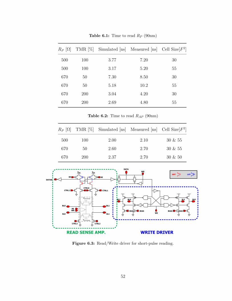
Table 6.1: Time to read RP (90nm)
RP [Ω] TMR [%] Simulated [ns] Measured [ns] Cell Size[F 2]
500 100 3.77 7.20 30
500 100 3.17 5.20 55
670 50 7.30 8.50 30
670 50 5.18 10.2 55
670 200 3.04 4.20 30
670 200 2.69 4.80 55
Table 6.2: Time to read RAP (90nm)
RP [Ω] TMR [%] Simulated [ns] Measured [ns] Cell Size[F 2]
500 100 2.00 2.10 30 & 55
670 50 2.60 2.70 30 & 55
670 200 2.37 2.70 30 & 50
RE RE
CTRL1
BL0
SL0
BL1
SL1
CTRL0
CTRL1
BIAS BIAS
DATA
BIAS BIAS
BL0BL1 SL0SL1
DATAB
WR
READ SENSE AMP. WRITE DRIVER
WE
HVT LVT
REWR
VDD VDD
Vprecharge
CTRL2 CTRL2
Vprecharge
Figure 6.3: Read/Write driver for short-pulse reading.
52
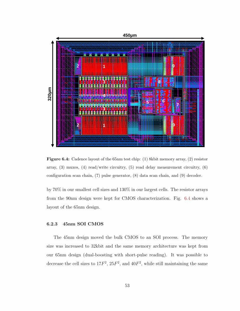
1
12
3
3
4
5 67
8
92
450µm
32
0µ
m
9
Figure 6.4: Cadence layout of the 65nm test chip: (1) 8kbit memory array, (2) resistor
array, (3) muxes, (4) read/write circuitry, (5) read delay measurement circuitry, (6)
configuration scan chain, (7) pulse generator, (8) data scan chain, and (9) decoder.
by 70% in our smallest cell sizes and 130% in our largest cells. The resistor arrays
from the 90nm design were kept for CMOS characterization. Fig. 6.4 shows a
layout of the 65nm design.
6.2.3 45nm SOI CMOS
The 45nm design moved the bulk CMOS to an SOI process. The memory
size was increased to 32kbit and the same memory architecture was kept from
our 65nm design (dual-boosting with short-pulse reading). It was possible to
decrease the cell sizes to 17F 2, 25F 2, and 40F 2, while still maintaining the same
53
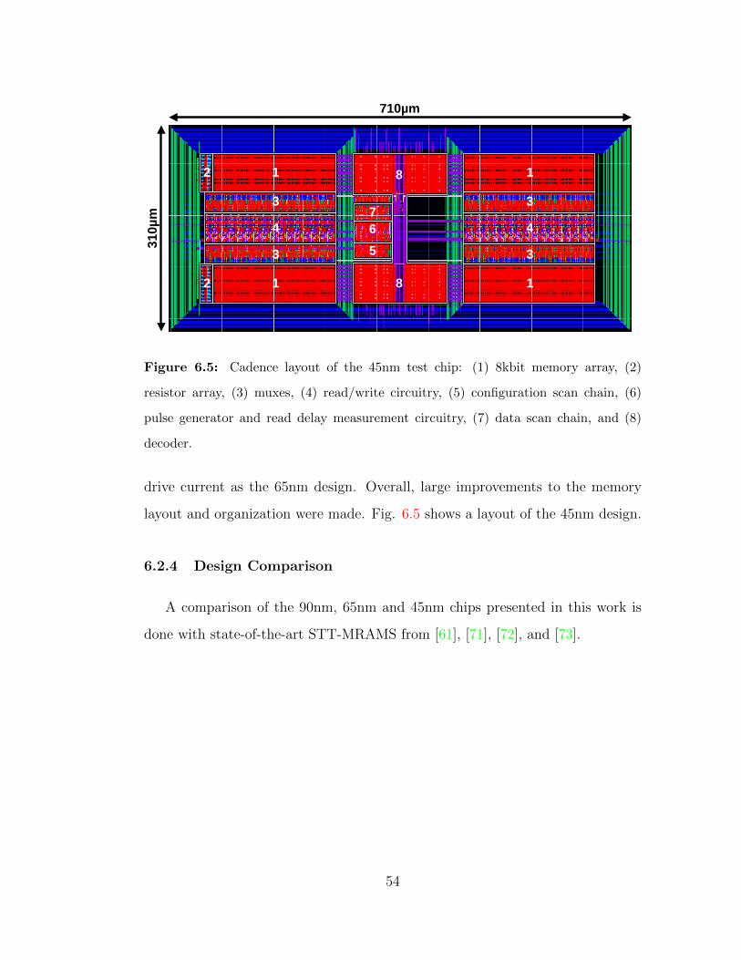
12
12
3
3
4
8
8
7
6
5
1
1
3
3
4
710µm
31
0µ
m
Figure 6.5: Cadence layout of the 45nm test chip: (1) 8kbit memory array, (2)
resistor array, (3) muxes, (4) read/write circuitry, (5) configuration scan chain, (6)
pulse generator and read delay measurement circuitry, (7) data scan chain, and (8)
decoder.
drive current as the 65nm design. Overall, large improvements to the memory
layout and organization were made. Fig. 6.5 shows a layout of the 45nm design.
6.2.4 Design Comparison
A comparison of the 90nm, 65nm and 45nm chips presented in this work is
done with state-of-the-art STT-MRAMS from [61], [71], [72], and [73].
54
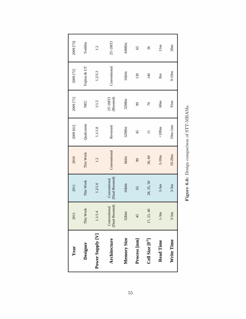
Yea
r
Cel
l S
ize
[F2]
Pro
cess
[n
m]
Rea
d T
ime
Wri
te T
ime
Mem
ory
Siz
e
Arc
hit
ectu
re
Des
ign
er
Pow
er S
up
ply
[V
]
2011
17, 25, 40
45
1-3
ns
3-5
ns
32kbit
Conven
tional
(Dual
-Boost
ed)
This
Work
1.1
/1.4
2009 [
61]
11
45
<100ns
10ns-
1m
s
32M
bit
Rev
erse
d
Qual
com
m
1.1
/1.8
2011
28, 35, 50
65
3-5
ns
3-5
ns
16kbit
Conven
tional
(Dual
-Boost
ed)
This
Work
1.2
/1.6
2010
30, 60
90
3-1
0ns
10-2
0ns
6kbit
Conven
tional
This
Work
1.2
2009 [
71]
70
90
60ns
91ns
32M
bit
2T
-1M
TJ
(Boost
ed)
NE
C
1/1
.5
2009 [
72]
140
130
8ns
9-1
0ns
16kbit
Conven
tional
Fuji
tsu &
UT
1.2
/3.3
2009 [
73]
36
65
11ns
30ns
64M
bit
2T
-1M
TJ
Tosh
iba
1.2
Figure
6.6:
Des
ign
com
par
ison
ofS
TT
-MR
AM
s.
55
CHAPTER 7
Conclusion
The potential for STT-MRAM to become a true universal memory has been
advanced by fabricating three test chips that demonstrate increased memory
densities and performance when compared to published state-of-the-art STT-
MRAMs. The 45nm test chip has a memory density 3.8 times greater on average
when compared to published state-of-the-art STT-MRAMs. It has read access
times ranging from 5 to 100 times faster, and is capable of delivering over 500µA
of drive current to write in less than 5ns. While MTJ/CMOS integration was not
accomplished, for reasons outside of our control, the chip represents the next step
forward in making STT-MRAM a true universal memory. Analysis of the future
scalability of MTJs shows that with a 22nm technology node, STT-MRAM will
be able to achieve Flash-like densities, with sub-nanosecond performance, while
using ten times less power.
7.1 Summary of Research Contributions
Specific accomplishments of this research are:
• Development of a physics-based MTJ macro-model capable of accurately
modeling and predicting device behavior across temperature. The model
was implemented in Verilog-A.
56
• Development of a design-space analysis toolset specifically for STT-MRAMs.
These tools allowed an accurate and fair assessment of different memory
architectures at the same time in order to maximize design margin, and
minimize power and area for a fixed level of performance.
• Design of three STT-MRAM test chips:
90nm bulk CMOS: 6kbit memory array, 2.5x density improvement over
SRAM, 2-10ns read, 200µA write current.
65nm bulk CMOS: 16kbit memory array, 4.3x density improvement
over SRAM, new high-speed read/write architecture, 400µA write cur-
rent.
45nm SOI CMOS: 32kbit memory array, 7.1x density improvement
over SRAM, average 3.8x density improvement over state-of-the-art
STT-MRAMs, 500µA write current.
7.2 Future Work
Additional steps required to demonstrate that STT-MRAM can be developed
into a true universal memory are:
• Extend the compact MTJ model to include localized heating effects, the
backhopping phenomenon, and noise models.
• Explore stacked memory architecture to improve cell density.
• Continue to refine the DSM and DSS of the design-space analysis tools for
integration with circuit simulators.
• Finalize the fabrication flow for MTJ/CMOS integration, including running
performance and yield characterizations on an integrated 45nm test chip.
57
References
[1] S. A. Wolf et al., “The Promise of Nanomagnetics and Spintronics for FutureLogic and Universal Memory,” Proceedings of the IEEE, vol. 98, no. 12, pp.2155 –2168, December 2010. 2, 3, 6, 7, 8, 9
[2] J. C. Slonczewski, “Current-Driven Excitation of Magnetic Multilayers,”Journal of Magnetism and Magnetic Materials, vol. 159, no. 1-2, pp. L1–L7, 1996. 3, 12, 13, 19
[3] I. Zutic, J. Fabian, and S. Das Sarma, “Spintronics: Fundamentals andApplications,” Rev. Mod. Phys., vol. 76, no. 2, pp. 323–410, April 2004. 6,7, 9, 10, 12
[4] Y. C. Tao and J. G. Hu, “Superconducting Spintronics: Spin-PolarizedTransport in Superconducting Junctions with Ferromagnetic Semiconduct-ing Contact,” Journal of Applied Physics, vol. 107, no. 4, 2010. 6, 9
[5] M. Julliere, “Tunneling Between Ferromagnetic Films,” Physics Letters A,vol. 54, no. 3, pp. 225–226, 1975. 7, 15
[6] M. E. Flatte, “Spintronics,” IEEE Transactions on Electron Devices, vol. 54,no. 5, pp. 907–920, May 2007. 7, 9, 10
[7] S. J. Pearton et al., “Spintronics Device Concepts,” Circuits, Devices andSystems, IEE Proceedings, vol. 152, no. 4, pp. 312–322, August 2005. 7, 9,10
[8] J. Mathon and A. Umerski, “Theory of Runneling Magnetoresistance ofan Epitaxial Fe/MgO/Fe(001) Junction,” Phys. Rev. B, vol. 63, no. 22, p.220403, May 2001. 7
[9] S. Das Sarma, J. Fabian, X. Hu, and I. Zutic, “Issues, Concepts, and Chal-lenges in Spintronics,” in IEEE 58th DRC (Device Research Conference)Conference Digest, June 2000, pp. 95–98. 7
[10] S. Kos et al., “Modeling Spin-Polarized Electron Transport in Semiconduc-tors for Spintronics Applications,” Computing in Science Engineering, vol. 9,no. 5, pp. 46–52, September-October 2007. 9
[11] M. E. Flatte, Z. G. Yu, E. Johnston-Halperin, and D. D. Awschalom, “The-ory of Semiconductor Magnetic Bipolar Transistors,” Applied Physics Let-ters, vol. 82, no. 26, pp. 4740–4742, 2003. 9
58
[12] S. Chakrabarti et al., “Spin-Polarized Light-Emitting Diodes with Mn-Doped InAs Quantum Dot Nanomagnets as a Spin Aligner,” Nano Letters,vol. 5, no. 2, pp. 209–212, 2005. 10
[13] P. Bruno, Y. Suzuki, and C. Chappert, “Magneto-optical Kerr Effect in aParamagnetic Overlayer on a Ferromagnetic Substrate: A Spin-PolarizedQuantum Size Effect,” Phys. Rev. B, vol. 53, no. 14, pp. 9214–9220, April1996. 10
[14] J. Z. Sun, “Spin Angular Momentum Transfer in Current-PerpendicularNanomagnetic Junctions,” IBM Journal of Research and Development,vol. 50, no. 1, pp. 81–100, January 2006. 11, 12
[15] Z. Diao et al., “Spin Transfer Switching in Dual MgO Magnetic TunnelJunctions,” Applied Physics Letters, vol. 90, no. 13, p. 132508, 2007. 12
[16] W. Zhu, H. Li, Y. Chen, and X. Wang, “Current Switching in MgO-BasedMagnetic Tunneling Junctions,” Magnetics, IEEE Transactions on, vol. 47,no. 1, pp. 156–160, January 2011. 12, 31
[17] K. Lee and S. Kang, “Control of Switching Current Asymmetry by Magne-tostatic Field in MgO-Based Magnetic Tunnel Junctions,” Electron DeviceLetters, IEEE, vol. 30, no. 12, pp. 1353–1355, December 2009. 12
[18] X. Yao, H. Meng, Y. Zhang, and J.-P. Wang, “Improved Current SwitchingSymmetry of Magnetic Tunneling Junction and Giant MagnetoresistanceDevices with Nano-Current-Channel Structure,” Journal of Applied Physics,vol. 103, no. 7, p. 07A717, 2008. 12
[19] R. H. Koch, J. A. Katine, and J. Z. Sun, “Time-Resolved Reversal of Spin-Transfer Switching in a Nanomagnet,” Phys. Rev. Lett., vol. 92, no. 8, p.088302, February 2004. 12, 13
[20] H. W. Schumacher et al., “Precessional Switching of the Magnetizationin Microscopic Magnetic Tunnel Junctions (Invited),” Journal of AppliedPhysics, vol. 93, no. 10, pp. 7290–7294, 2003. 12
[21] T. L. Gilbert, “A Phenomenological Theory of Damping in FerromagneticMaterials,” IEEE Transactions on Magnetics, vol. 40, no. 6, pp. 3443–3449,November 2004. 12
[22] L. Landau and E. Lifshitz, “On the Theory of the Dispersion of MagneticPermeability in Ferromagnetic Bodies,” Physikalische zeitschrift der Sowje-tunion, vol. 8, pp. 153–169, 1935. 12
59
[23] T. Moriyama et al., “Tunnel Magnetoresistance and Spin Torque Switchingin MgO-based Magnetic Tunnel Junctions with a Co/Ni Multilayer Elec-trode,” Applied Physics Letters, vol. 97, no. 7, p. 072513, 2010. 13, 18,19
[24] Z. M. Zeng et al., “Effect of resistance-area product on spin-transfer switch-ing in mgo-based magnetic tunnel junction memory cells,” Applied PhysicsLetters, vol. 98, no. 7, p. 072512, 2011. 14
[25] Y. Higo et al., “Thermal Activation Effect on Spin Transfer Switching inMagnetic Tunnel Junctions,” Applied Physics Letters, vol. 87, no. 8, p.082502, 2005. 14
[26] M. Pakala et al., “Critical Current Distribution in Spin-Transfer-SwitchedMagnetic Tunnel Junctions,” Journal of Applied Physics, vol. 98, no. 5, p.056107, 2005. 14
[27] T. Aoki, Y. Ando, M. Oogane, and H. Naganuma, “Reproducible Trajectoryon Subnanosecond Spin-Torque Magnetization Switching Under a Zero-BiasField for MgO-Based Ferromagnetic Tunnel Junctions,” Applied Physics Let-ters, vol. 96, no. 14, p. 142502, 2010. 14
[28] E. R. Nowak, M. B. Weissman, and S. S. P. Parkin, “Electrical Noise inHysteretic Ferromagnet–Insulator–Ferromagnet Tunnel Junctions,” AppliedPhysics Letters, vol. 74, no. 4, pp. 600–602, 1999. 14, 17
[29] S. X. Huang, T. Y. Chen, and C. L. Chien, “Spin Polarization of AmorphousCoFeB Determined by Point-Contact Andreev Reflection,” Applied PhysicsLetters, vol. 92, no. 24, p. 242509, 2008. 15
[30] J. S. Moodera and G. Mathon, “Spin Polarized Tunneling in FerromagneticJunctions,” Journal of Magnetism and Magnetic Materials, vol. 200, no. 1-3,pp. 248 – 273, 1999. 15
[31] Y. Lu et al., “Bias Voltage and Temperature Dependence of Magnetotun-neling Effect,” Journal of Applied Physics, vol. 83, no. 11, pp. 6515–6517,1998. 15, 16, 22
[32] X. Liu et al., “Thermal Stability of Magnetic Tunneling Junctions with MgOBarriers for High Temperature Spintronics,” Applied Physics Letters, vol. 89,no. 2, p. 023504, 2006. 15
[33] C. H. Shang, J. Nowak, R. Jansen, and J. S. Moodera, “Temperature De-pendence of Magnetoresistance and Surface Magnetization in Ferromagnetic
60
Tunnel Junctions,” Phys. Rev. B, vol. 58, no. 6, pp. R2917–R2920, August1998. 15, 21, 23
[34] J. G. Simmons, “Generalized Formula for the Electric Tunnel Effect betweenSimilar Electrodes Separated by a Thin Insulating Film,” Journal of AppliedPhysics, vol. 34, no. 6, pp. 1793–1803, 1963. 15
[35] T. Zhu, X. Xiang, and J. Q. Xiao, “Bias Dependence of Tunneling Mag-netoresistance on Ferromagnetic Electrode Thickness,” Applied Physics Let-ters, vol. 82, no. 16, pp. 2676–2678, 2003. 15
[36] G. G. Cabrera and N. Garcıa, “Low Voltage I–V Characteristics in MagneticTunneling Junctions,” Applied Physics Letters, vol. 80, no. 10, pp. 1782–1784, 2002. 15
[37] S. Chatterjee, S. Salahuddin, S. Kumar, and S. Mukhopadhyay, “Analysisof Thermal Behaviors of Spin-Torque-Transfer RAM: A Simulation Study,”in Low-Power Electronics and Design (ISLPED), 2010 ACM/IEEE Inter-national Symposium on, August 2010, pp. 13–18. 16
[38] Y. Zhang et al., “Micromagnetic Study of Hotspot and Thermal Effects onSpin-Transfer Switching in Magnetic Tunnel Junctions,” Journal of AppliedPhysics, vol. 101, no. 10, p. 103905, 2007. 16
[39] S. Chaudhuri et al., “Design of TAS-MRAM Prototype for NV EmbeddedMemory Applications,” in Memory Workshop (IMW), 2010 IEEE Interna-tional, May 2010, pp. 1 –4. 16
[40] J. Z. Sun et al., “High-Bias Backhopping in Nanosecond Time-Domain Spin-Torque Switches of MgO-based Magnetic Tunnel Junctions,” Journal of Ap-plied Physics, vol. 105, no. 7, p. 07D109, 2009. 16, 17
[41] T. Min et al., “Back-Hopping after Spin Torque Transfer Induced Magneti-zation Switching in Magnetic Tunneling Junction Cells,” Journal of AppliedPhysics, vol. 105, no. 7, p. 07D126, 2009. 16, 17
[42] S. Ingvarsson et al., “Low-Frequency Magnetic Noise in Micron-Scale Mag-netic Tunnel Junctions,” Phys. Rev. Lett., vol. 85, no. 15, pp. 3289–3292,Oct 2000. 17
[43] K. B. Klaassen, J. C. L. van Peppen, and X. Xing, “Noise in MagneticTunnel Junction Devices,” Journal of Applied Physics, vol. 93, no. 10, pp.8573–8575, 2003. 17
61
[44] K. Shimazawa et al., “Frequency Response of Common Lead and ShieldType Magnetic Tunneling Junction Head,” Magnetics, IEEE Transactionson, vol. 37, no. 4, pp. 1684–1686, July 2001. 17
[45] A. F. M. Nor et al., “Low-Frequency Noise in MgO Magnetic Tunnel Junc-tions,” Journal of Applied Physics, vol. 99, no. 8, p. 08T306, 2006. 17
[46] Y. Huai, “Spin-Transfer Torque MRAM (STT-MRAM): Challenges andProspects,” AAPPS Bulletin, vol. 18, no. 6, pp. 33–40, December 2008.18
[47] B. F. Cockburn, “The Emergence of High-Density Semiconductor-Compati-ble Spintronic Memory,” in International Conference on MEMS, NANO andSmart Systems, 2003. Proceedings., July 2003, pp. 321–326. 18
[48] M. R. Scheinfein, “LLG Micromagnetics Simulator.” [Online]. Available:http://llgmicro.home.mindspring.com 18, 25
[49] J. Z. Sun, “Spin-Current Interaction with a Monodomain Magnetic Body:A Model Study,” Phys. Rev. B, vol. 62, no. 1, pp. 570–578, July 2000. 20
[50] J. A. Osborn, “Demagnetizing Factors of the General Ellipsoid,” Phys. Rev.,vol. 67, no. 11-12, pp. 351–357, June 1945. 20
[51] P. Weiss, “L’hypothese du Champ Moleculaire et la Propriete Ferro-magnetique,” J. Phys. Theor. Appl., vol. 6, no. 1, pp. 661–690, 1907. 21
[52] A. Raghunathan, Y. Melikhov, J. E. Snyder, and D. C. Jiles, “Modeling theTemperature Dependence of Hysteresis Based on Jiles-Atherton Theory,”IEEE Transactions on Magnetics, vol. 45, no. 10, pp. 3954–3957, October2009. 21
[53] X. Kou, J. Schmalhorst, A. Thomas, and G. Reiss, “Temperature Depen-dence of the Resistance of Magnetic Tunnel Junctions with MgO Barrier,”Applied Physics Letters, vol. 88, no. 21, p. 212115, 2006. 23, 24
[54] P. Padhan et al., “Frequency-Dependent Magnetoresistance and Magnetoca-pacitance Properties of Magnetic Tunnel Junctions with MgO Tunnel Bar-rier,” Applied Physics Letters, vol. 90, no. 14, p. 142105, 2007. 24
[55] P. Wisniowski et al., “Temperature Dependence of Tunnel Magnetoresistanceand Magnetization of IrMn Based MTJ,” Physica Status Solidi, vol. 201, pp.1648–1652, 2004. 23
62
[56] S. R. Min et al., “Etch Characteristics of Magnetic Tunnel Junction Stackwith Nanometer-Sized Patterns for Magnetic Random Access Memory,”Thin Solid Films, Proceedings of the International Symposium on Dry Pro-cess, 2006. (DPS 2006)., vol. 516, no. 11, pp. 3507–3511, November 2008.28
[57] R. Beach et al., “A Statistical Study of Magnetic Tunnel Junctions for High-Density Spin Torque Transfer-MRAM (STT-MRAM),” in Electron DevicesMeeting, 2008. IEDM 2008. IEEE International, December 2008, pp. 1–4.28
[58] V. Korenivski and R. Leuschner, “Thermally Activated Switching in Nano-scale Magnetic Tunnel Junctions,” IEEE Transactions on Magnetics, vol. 46,no. 6, pp. 2101–2103, June 2010. 29
[59] J. Sun and D. Ralph, “Magnetoresistance and Spin-Transfer Torque in Mag-netic Tunnel Junctions,” Journal of Magnetism and Magnetic Materials, vol.320, no. 7, pp. 1227–1237, 2008. 29
[60] H. Chang and J. Burns, “Demagnetizing and Stray Fields of EllipticalFilms,” Journal of Applied Physics, vol. 37, no. 8, pp. 3240–3245, July 1966.29
[61] C. J. Lin et al., “45nm Low Power CMOS Logic Compatible Embedded STTMRAM Utilizing a Reverse-Connection 1T/1MTJ Cell,” in Electron DevicesMeeting (IEDM), 2009 IEEE International, December 2009, pp. 1–4. 30, 54
[62] T. Takenaga et al., “Control of Pinned Layer Magnetization Direction inSpin-Valve-Type Magnetic Tunnel Junction with an IrMn Layer,” Journalof Applied Physics, vol. 95, no. 11, pp. 6795–6797, 2004. 30
[63] M. Motoyoshi et al., “A study for 0.18 µm high-density MRAM,” in Sym-posium on VLSI Technology, 2004. Digest of Technical Papers., June 2004,pp. 22–23. 37
[64] A. Raychowdhury, D. Somasekhar, T. Karnik, and V. De, “Design Space andScalability Exploration of 1T-1STT MTJ Memory Arrays in the Presence ofVariability and Disturbances,” in Electron Devices Meeting (IEDM), 2009IEEE International, December 2009, pp. 1–4. 37
[65] P. Amiri et al., “Low Write-Energy Magnetic Tunnel Junctions forHigh-Speed Spin-Transfer-Torque MRAM,” Electron Device Letters, IEEE,vol. 32, no. 1, pp. 57–59, January 2011. 48, 49
63
[66] P. K. Amiri et al., “Switching Current Reduction Using PerpendicularAnisotropy in CoFeB-MgO Magnetic Tunnel Junctions,” Applied PhysicsLetters, vol. 98, no. 11, p. 112507, 2011. 48, 49
[67] G. E. Rowlands et al., “Deep Subnanosecond Spin Torque Switching in Mag-netic Tunnel Junctions with Combined In-Plane and Perpendicular Polariz-ers,” Applied Physics Letters, vol. 98, no. 10, p. 102509, 2011. 48, 49
[68] W. Zhao et al., “New Non-Volatile Logic Based on Spin-MTJ,” physica statussolidi (a), vol. 205, no. 6, pp. 1373–1377, 2008. 48
[69] X. F. Han and A. C. C. Yu, “Patterned Magnetic Tunnel Junctions with AlConduction Layers: Fabrication and Reduction of Pinhole Effect,” Journalof Applied Physics, vol. 95, no. 2, pp. 764–766, 2004. 49
[70] S. Isogami, M. Tsunoda, and M. Takahashi, “30-nm Scale Fabrication ofMagnetic Tunnel Junctions using EB Assisted CVD Hard Masks,” Magnet-ics, IEEE Transactions on, vol. 41, no. 10, pp. 3607–3609, October 2005.49
[71] R. Nebashi et al., “A 90nm 12ns 32Mb 2T1MTJ MRAM,” in ISSCC 2009,February 2009, pp. 462–463, 463a. 54
[72] D. Halupka et al., “Negative-Resistance Read and Write Schemes for STT-MRAM in 0.13 µm CMOS,” in ISSCC 2010, February 2010, pp. 256–257.54
[73] K. Tsuchida et al., “A 64Mb MRAM with Clamped-Reference andAdequate-Reference Schemes,” in ISSCC 2010, February 2010, pp. 258–259.54
64

![Low Write-Energy STT-MRAMs using FinFET-based Access …sportlab.usc.edu › ~shafaei › pdf › iccd14.pdf · 2014-08-20 · accessed design [6] shows that under practical process](https://img.pdfslide.us/doc/110x75/5f18e5c38bf20a1df36c6819/low-write-energy-stt-mrams-using-finfet-based-access-a-shafaei-a-pdf-a-iccd14pdf.jpg)


![Modeling and Circuit Design of Associative Memories With ... · (MTJ-MRAM) [4] have been developed. Of these technolo-gies, FeFETs and two types of MTJ-MRAMs, switched by spin-transfer](https://img.pdfslide.us/doc/110x75/60502f0b19e64d4f2151d595/modeling-and-circuit-design-of-associative-memories-with-mtj-mram-4-have.jpg)