Embed Size (px)
Citation preview
MICROCOMPUTER MN1030/MN103S
MN1030/MN103S Series
Instruction Manual
Pub.No.13250-040E


PanaXSeries is a trademark of Matsushita Electric Industrial Co., Ltd.All other corporation names, logotype and product names written in this book are trademarks or registered trademarks of their respective corporations.
Request for your special attention and precautions in using the technical information and semiconductors described in this book
(1) An export permit needs to be obtained from the competent authorities of the Japanese Government if any of the products or technologies described in this book and controlled under the "Foreign Exchange and Foreign Trade Law" is to be exported or taken out of Japan.
(2) The technical information described in this book is limited to showing representative characteristics and applied circuits examples of the products. It neither warrants non-infringement of intellectual property right or any other rights owned by our company or a third party, nor grants any license.
(3) We are not liable for the infringement of rights owned by a third party arising out of the use of the product or technologies as described in this book.
(4) The products described in this book are intended to be used for standard applications or general electronic equipment (such as office equipment, communications equipment, measuring instruments and household appliances).Consult our sales staff in advance for information on the following applications:
• Special applications (such as for airplanes, aerospace, automobiles, traffic control equipment, combustion equipment, life support systems and safety devices) in which exceptional quality and reliability are required, or if the failure or malfunction of the products may directly jeopardize life or harm the human body.
• Any applications other than the standard applications intended.
(5) The products and product specifications described in this book are subject to change without notice for modification and/or improvement. At the final stage of your design, purchasing, or use of the products, therefore, ask for the most up-to-date Product Standards in advance to make sure that the latest specifications satisfy your requirements.
(6) When designing your equipment, comply with the guaranteed values, in particular those of maximum rating, the range of operating power supply voltage, and heat radiation characteristics. Otherwise, we will not be liable for any defect which may arise later in your equipment.Even when the products are used within the guaranteed values, take into the consideration of incidence of break down and failure mode, possible to occur to semiconductor products. Measures on the systems such as redundant design, arresting the spread of fire or preventing glitch are recommended in order to prevent physical injury, fire, social damages, for example, by using the products.
(7) When using products for which damp-proof packing is required, observe the conditions (including shelf life and amount of time let standing of unsealed items) agreed upon when specification sheets are individually exchanged.
(8) This book may be not reprinted or reproduced whether wholly or partially, without the prior written permission of Matsushita Electric Industrial Co., Ltd.
If you have any inquiries or questions about this book or our semiconductors, please contact one of our sales offices listed at the back of this book.
< About This Manual - 1 >
This document contains a detailed description of the instruction set for the MN1030/MN103S Series.
This document concentrates on the AM32 microcontroller core. When the specifications differ between cores,
separate descriptions appear next to icons indicating the appropriate core or cores
Chapter 1 provides an overview of the instruction set--instruction functions, formats, and the like.
Chapter 2 contains detailed descriptions of the individual instructions--operation, effect on PSW flags, and the like.
Chapter 3 contains usage notes--a description of the pipeline architecture, programming notes, usage
recommendations, and the like.
The Appendix contains charts for the entire instruction set and instruction mappings.
■ Finding Information
This document incorporates the following aids for locating necessary information as quickly as possible.
(1) Index tabs in the inside margins of left-hand pages indicate Chapters.
(2) The table of contents near the beginning of this document lists section headings.
(3) As you flip through the document, the page header gives the chapter; the footer, the section heading.
(4) The index near the end of this document lists page references for all instructions and instruction variants.
In Chapter 2, the instruction mnemonic appears in the page footer for right-hand pages.
■ Related Manuals
The following related manuals are available. Please contact our sales representative for more details.
< For MN1030 Series Users >
MN1030 Series Cross Assembler User's Manual
<Describes the assembler syntax and notation>
MN1030 Series C Compiler User's Manual: Usage Guide
<Describes the installation, the commands, and options of the C Compiler>
MN1030/MN103S/MN103E Series C Compiler User's Manual: Language Description
<Describes the syntax of the C Compiler>
MN1030/MN103S/MN103E Series C Compiler User's Manual: Library Reference
<Describes the the standard library of the C Compiler>
MN1030/MN103S Series C Source Code Debugger for Windows® User's Manual
<Describes the use of the C source code debugger for Windows®>
MN1030/MN103S Series Installation Manual
<Describes the installation of the C compiler, cross-assembler and C source code debugger and the
procedure for bringing up the in-circuit emulator>
About This Manual
< About This Manual - 2 >
< For MN103S Series Users >
MN103S Series Cross Assembler User's Manual
<Describes the assembler syntax and notation>
MN103S Series C Compiler User's Manual: Usage Guide
<Describes the installation, the commands, and options of the C Compiler>
MN1030/MN103S/MN103E Series C Compiler User's Manual: Language Description
<Describes the syntax of the C Compiler>
MN1030/MN103S/MN103E Series C Compiler User's Manual: Library Reference
<Describes the the standard library of the C Compiler>
MN1030/MN103S Series C Source Code Debugger for Windows® User's Manual
<Describes the use of the C source code debugger for Windows®>
MN1030/MN103S Series Installation Manual
<Describes the installation of the C compiler, cross-assembler and C source code debugger and the
procedure for bringing up the in-circuit emulator>
< About This Manual - 3 >
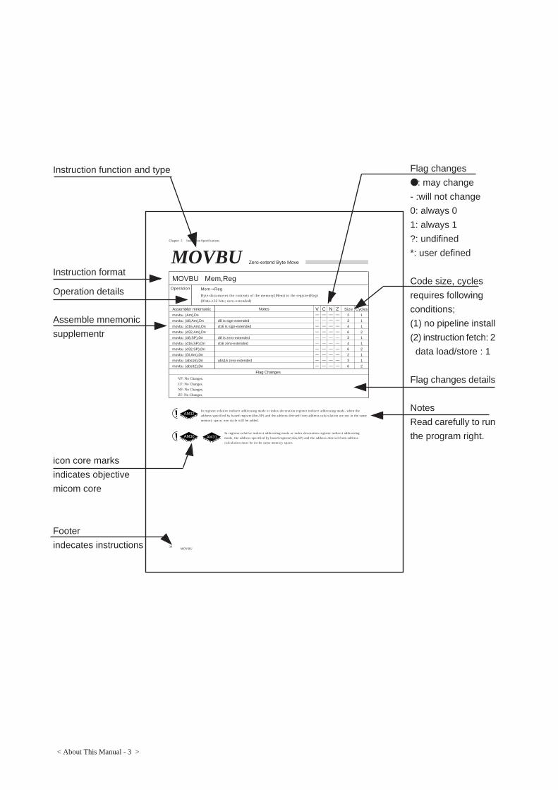
Instruction function and type
Instruction format
Operation details
Assemble mnemonic
supplementr
icon core marks
indicates objective
micom core
Footer
indecates instructions
Chapter 2 Instruction Specifications
30
MOVBU Zero-extend Byte Move
MOVBU Mem,RegOperation Mem→Reg
Byte-data-moves the contents of the memory(Mem) to the register(Reg)
(8 bits→32 bits; zero-extended)
Assembler mnemonic Size Cycles
movbu (Am),Dn
movbu (d8,Am),Dn d8 is sign-extended
movbu (d16,Am),Dn d16 is sign-extended
movbu (d32,Am),Dn
movbu (d8,SP),Dn d8 is zero-extended
movbu (d16,SP),Dn d16 zero-extended
movbu (d32,SP),Dn
movbu (Di,Am),Dn
movbu (abs16),Dn abs16 zero-extended
movbu (abs32),Dn
Notes
Flag Changes
VF: No Changes.
CF: No Changes.
NF: No Changes.
ZF: No Changes.
2
3
4
6
3
4
6
2
3
6
1
1
1
2
1
1
2
1
1
2
MOVBU
V C ZN—
—
—
—
—
—
—
—
—
—
—
—
—
—
—
—
—
—
—
—
—
—
—
—
—
—
—
—
—
—
—
—
—
—
—
—
—
—
—
—
In register-relative indirect addressing mode or index decoration register indirect addressing
mode, the address specified by based register(Am,SP) and the address derived from address
calculation must be in the same memory space.
AM30 AM31
In register-relative indirect addressing mode or index decoration register indirect addressing mode, when the
address specified by based register(Am,SP) and the address derived from address caluculation are not in the same
memory space, one cycle will be added.
AM32
Flag changes
● : may change
- :will not change
0: always 0
1: always 1
?: undifined
*: user defined
Code size, cycles
requires following
conditions;
(1) no pipeline install
(2) instruction fetch: 2
data load/store : 1
Flag changes details
Notes
Read carefully to run
the program right.
< About This Manual - 4 >
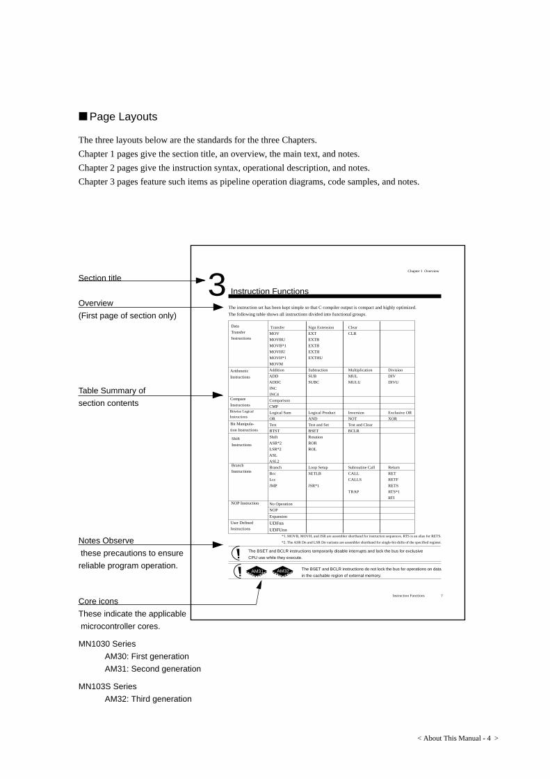
■ Page Layouts
The three layouts below are the standards for the three Chapters.
Chapter 1 pages give the section title, an overview, the main text, and notes.
Chapter 2 pages give the instruction syntax, operational description, and notes.
Chapter 3 pages feature such items as pipeline operation diagrams, code samples, and notes.
Section title
Overview
(First page of section only)
Table Summary of
section contents
Notes Observe
these precautions to ensure
reliable program operation.
Core icons
These indicate the applicable
microcontroller cores.
MN1030 Series
AM30: First generation
AM31: Second generation
MN103S Series
AM32: Third generation
7
Chapter 1 Overview
Instruction Functions
3
Bitwise Logical
Instructions
Instruction Functions
The instruction set has been kept simple so that C compiler output is compact and highly optimized.
The following table shows all instructions divided into functional groups.
Transfer Sign Extension Clear
MOV EXT CLR
MOVBU EXTB
MOVB*1 EXTB
MOVHU EXTH
MOVH*1 EXTHU
MOVM
Addition Subtraction Multiplication Division
ADD SUB MUL DIV
ADDC SUBC MULU DIVU
INC
INC4
Comparison
CMP
Logical Sum Logical Product Inversion Exclusive OR
OR AND NOT XOR
Test Test and Set Test and Clear
BTST BSET BCLR
Shift Rotation
ASR*2 ROR
LSR*2 ROL
ASL
ASL2
Branch Loop Setup Subroutine Call Return
Bcc SETLB CALL RET
Lcc CALLS RETF
JMP JSR*1 RETS
TRAP RTS*1
RTI
No Operation
NOP
Expansion
UDFnn
UDFUnn*1. MOVB, MOVH, and JSR are assembler shorthand for instruction sequences. RTS is an alias for RETS.
*2. The ASR Dn and LSR Dn variants are assembler shorthand for single-bit shifts of the specified register.
The BSET and BCLR instructions temporarily disable interrupts and lock the bus for exclusive
CPU use while they execute.
The BSET and BCLR instructions do not lock the bus for operations on data
in the cachable region of external memory.
Data
Transfer
Instructions
Arithmetic
Instructions
Compare
Instructions
Bit Manipula-
tion Instructions
Shift
Instructions
Branch
Instructions
NOP Instruction
User Defined
Instructions
AM32AM31
< About This Manual - 5 >
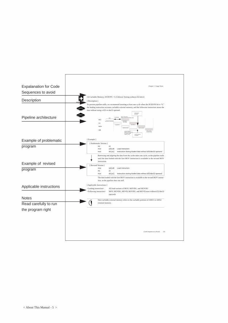
Expalanation for Code
Sequences to avoid
Description
Pipeline architecture
Example of problematic
program
Example of revised
program
Applicable instructions
Notes
Read carefully to run
the program right
131
Chapter 3 Usage Notes
(3) Cachable Memory, DCBYPS = 0, Follower Storing without d32/abs32
[ Description ]
To prevent pipeline stalls, we recommend inserting at least one cycle when the DCBYPS bit is “0,”
the leading instruction accesses cachable external memory, and the following instruction stores the
data without using a d32 or abs32 operand.
[ Example ]
[ Problematic Version ]
inc a1
mov (a0),d0 Load instruction
mov d0,(a1) Instruction storing loaded data without d32/abs32 operand
Retrieving and aligning the data from the cache takes one cycle, so the pipeline stalls
until the data loaded with the first MOV instruction is available to the second MOV
instruction.
[ Revised Version ]
mov (a0),d0 Load instruction
inc a1
mov d0,(a1) Instruction storing loaded data without d32/abs32 operand
The data loaded with the first MOV instruction is available to the second MOV instruc-
tion, so the pipeline does not stall.
[ Applicable Instructions ]
<Leading instruction> All load variants of MOV, MOVBU, and MOVHU
<Following instruction> MOV, MOVBU, MOVB, MOVHU, and MOVH store without d32/abs32
operands
Here cachable external memory refers to the cachable portions of AM31 or AM32
external memory.
Code Sequences to Avoid
High-speed
AM31
AM32
cache access
DEC
MEM
EX
WB
instruction decoding
calculation
1cycle gap
instruction decoding
load
cache readout/alignment/extension of memory data/register write
cache data available
write cache readout-data
cache readout complete
Store instruction without 32-bit immediate value
cache access
calculation
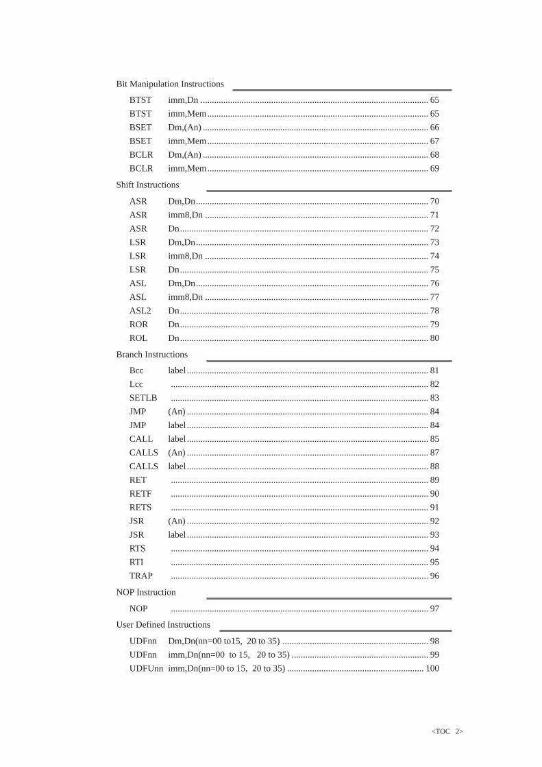
Table of Contents
Chapter 1 Overview
Chapter 2 Instruction Specifications
Chapter 3 Usage Notes
Appendix
Index
012345
<TOC 1>
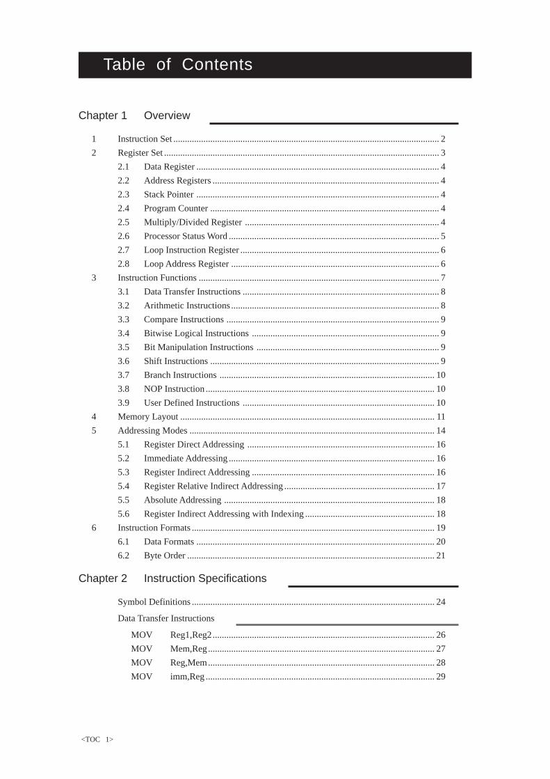
Table of Contents
Chapter 1 Overview
1 Instruction Set ................................................................................................................... 2
2 Register Set ....................................................................................................................... 3
2.1 Data Register ......................................................................................................... 4
2.2 Address Registers .................................................................................................. 4
2.3 Stack Pointer ......................................................................................................... 4
2.4 Program Counter ................................................................................................... 4
2.5 Multiply/Divided Register .................................................................................... 4
2.6 Processor Status Word ........................................................................................... 5
2.7 Loop Instruction Register ...................................................................................... 6
2.8 Loop Address Register .......................................................................................... 6
3 Instruction Functions ........................................................................................................ 7
3.1 Data Transfer Instructions ..................................................................................... 8
3.2 Arithmetic Instructions .......................................................................................... 8
3.3 Compare Instructions ............................................................................................ 9
3.4 Bitwise Logical Instructions ................................................................................. 9
3.5 Bit Manipulation Instructions ............................................................................... 9
3.6 Shift Instructions ................................................................................................... 9
3.7 Branch Instructions ............................................................................................. 10
3.8 NOP Instruction ................................................................................................... 10
3.9 User Defined Instructions ................................................................................... 10
4 Memory Layout .............................................................................................................. 11
5 Addressing Modes .......................................................................................................... 14
5.1 Register Direct Addressing ................................................................................. 16
5.2 Immediate Addressing ......................................................................................... 16
5.3 Register Indirect Addressing ............................................................................... 16
5.4 Register Relative Indirect Addressing ................................................................. 17
5.5 Absolute Addressing ........................................................................................... 18
5.6 Register Indirect Addressing with Indexing ........................................................ 18
6 Instruction Formats ......................................................................................................... 19
6.1 Data Formats ....................................................................................................... 20
6.2 Byte Order ........................................................................................................... 21
Chapter 2 Instruction Specifications
Symbol Definitions ......................................................................................................... 24
Data Transfer Instructions
MOV Reg1,Reg2................................................................................................ 26
MOV Mem,Reg.................................................................................................. 27
MOV Reg,Mem.................................................................................................. 28
MOV imm,Reg ................................................................................................... 29
<TOC 2>
Bit Manipulation Instructions
BTST imm,Dn .................................................................................................... 65
BTST imm,Mem................................................................................................. 65
BSET Dm,(An) ................................................................................................... 66
BSET imm,Mem................................................................................................. 67
BCLR Dm,(An) ................................................................................................... 68
BCLR imm,Mem................................................................................................. 69
Shift Instructions
ASR Dm,Dn...................................................................................................... 70
ASR imm8,Dn .................................................................................................. 71
ASR Dn............................................................................................................. 72
LSR Dm,Dn...................................................................................................... 73
LSR imm8,Dn .................................................................................................. 74
LSR Dn............................................................................................................. 75
ASL Dm,Dn...................................................................................................... 76
ASL imm8,Dn .................................................................................................. 77
ASL2 Dn............................................................................................................. 78
ROR Dn............................................................................................................. 79
ROL Dn............................................................................................................. 80
Branch Instructions
Bcc label .......................................................................................................... 81
Lcc ................................................................................................................. 82
SETLB ................................................................................................................. 83
JMP (An) .......................................................................................................... 84
JMP label .......................................................................................................... 84
CALL label .......................................................................................................... 85
CALLS (An) .......................................................................................................... 87
CALLS label .......................................................................................................... 88
RET ................................................................................................................. 89
RETF ................................................................................................................. 90
RETS ................................................................................................................. 91
JSR (An) .......................................................................................................... 92
JSR label .......................................................................................................... 93
RTS ................................................................................................................. 94
RTI ................................................................................................................. 95
TRAP ................................................................................................................. 96
NOP Instruction
NOP ................................................................................................................. 97
User Defined Instructions
UDFnn Dm,Dn(nn=00 to15, 20 to 35) ................................................................ 98
UDFnn imm,Dn(nn=00 to 15, 20 to 35) ............................................................ 99
UDFUnn imm,Dn(nn=00 to 15, 20 to 35) ............................................................ 100
<TOC 3>
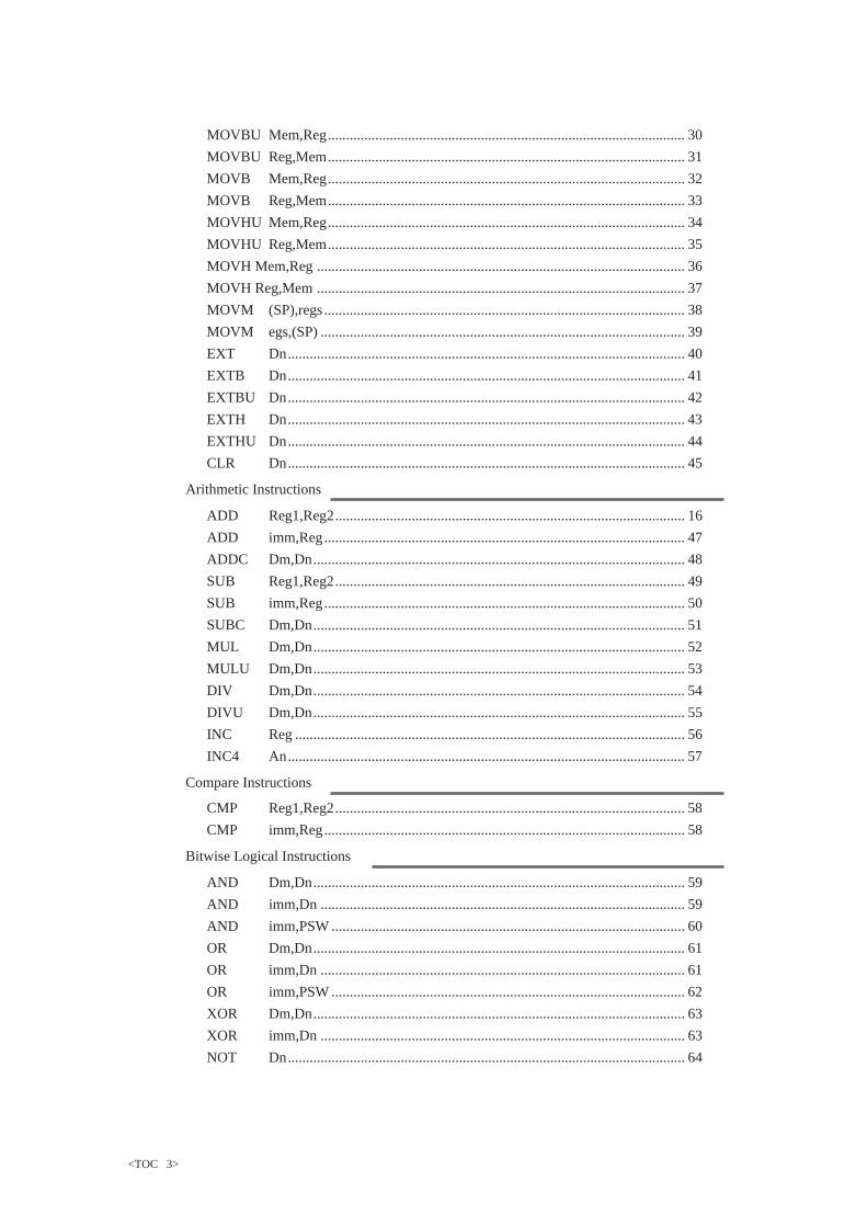
MOVBU Mem,Reg.................................................................................................. 30
MOVBU Reg,Mem.................................................................................................. 31
MOVB Mem,Reg.................................................................................................. 32
MOVB Reg,Mem.................................................................................................. 33
MOVHU Mem,Reg.................................................................................................. 34
MOVHU Reg,Mem.................................................................................................. 35
MOVH Mem,Reg ..................................................................................................... 36
MOVH Reg,Mem ..................................................................................................... 37
MOVM (SP),regs................................................................................................... 38
MOVM egs,(SP) .................................................................................................... 39
EXT Dn............................................................................................................. 40
EXTB Dn............................................................................................................. 41
EXTBU Dn............................................................................................................. 42
EXTH Dn............................................................................................................. 43
EXTHU Dn............................................................................................................. 44
CLR Dn............................................................................................................. 45
Arithmetic Instructions
ADD Reg1,Reg2................................................................................................ 16
ADD imm,Reg................................................................................................... 47
ADDC Dm,Dn...................................................................................................... 48
SUB Reg1,Reg2................................................................................................ 49
SUB imm,Reg................................................................................................... 50
SUBC Dm,Dn...................................................................................................... 51
MUL Dm,Dn...................................................................................................... 52
MULU Dm,Dn...................................................................................................... 53
DIV Dm,Dn...................................................................................................... 54
DIVU Dm,Dn...................................................................................................... 55
INC Reg ........................................................................................................... 56
INC4 An............................................................................................................. 57
Compare Instructions
CMP Reg1,Reg2................................................................................................ 58
CMP imm,Reg................................................................................................... 58
Bitwise Logical Instructions
AND Dm,Dn...................................................................................................... 59
AND imm,Dn .................................................................................................... 59
AND imm,PSW ................................................................................................. 60
OR Dm,Dn...................................................................................................... 61
OR imm,Dn .................................................................................................... 61
OR imm,PSW ................................................................................................. 62
XOR Dm,Dn...................................................................................................... 63
XOR imm,Dn .................................................................................................... 63
NOT Dn............................................................................................................. 64
<TOC 4>
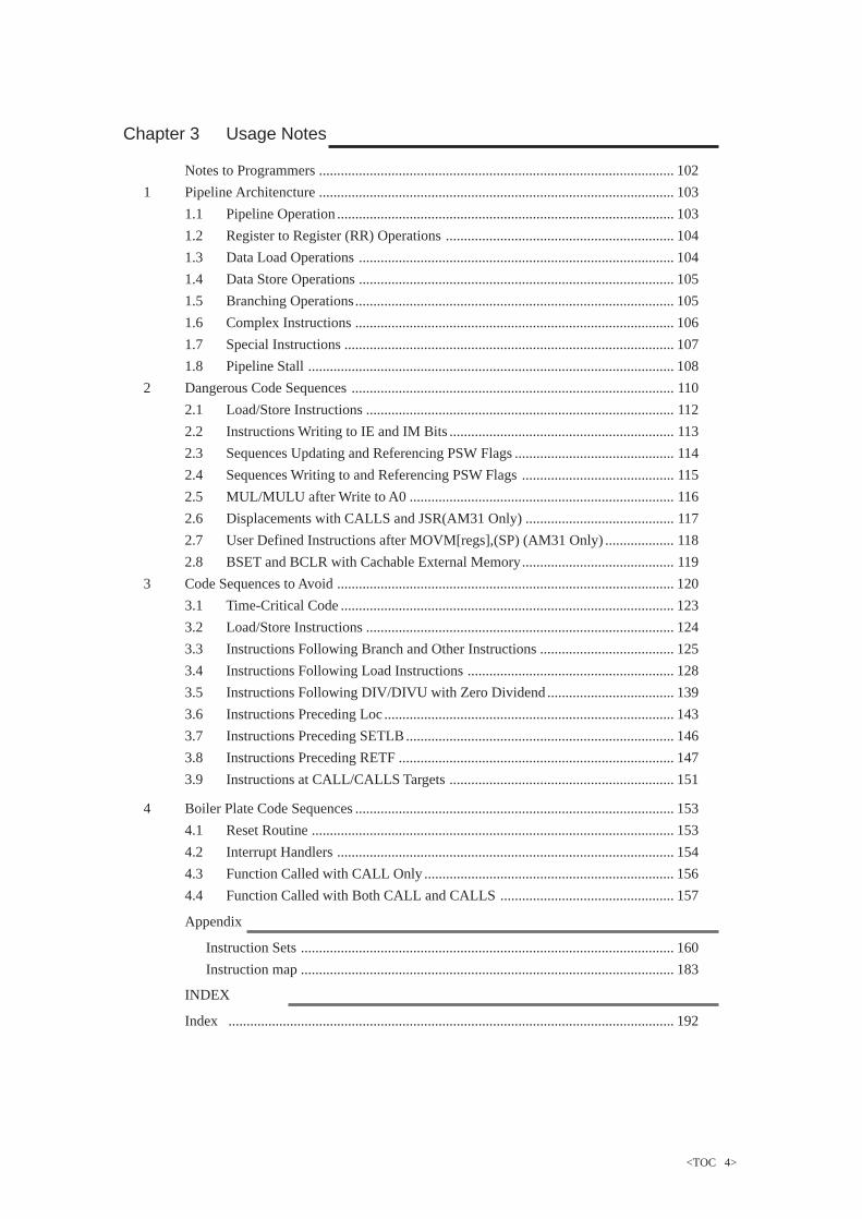
Chapter 3 Usage Notes
Notes to Programmers .................................................................................................. 102
1 Pipeline Architencture .................................................................................................. 103
1.1 Pipeline Operation ............................................................................................. 103
1.2 Register to Register (RR) Operations ............................................................... 104
1.3 Data Load Operations ....................................................................................... 104
1.4 Data Store Operations ....................................................................................... 105
1.5 Branching Operations........................................................................................ 105
1.6 Complex Instructions ........................................................................................ 106
1.7 Special Instructions ........................................................................................... 107
1.8 Pipeline Stall ..................................................................................................... 108
2 Dangerous Code Sequences ......................................................................................... 110
2.1 Load/Store Instructions ..................................................................................... 112
2.2 Instructions Writing to IE and IM Bits .............................................................. 113
2.3 Sequences Updating and Referencing PSW Flags ............................................ 114
2.4 Sequences Writing to and Referencing PSW Flags .......................................... 115
2.5 MUL/MULU after Write to A0 ......................................................................... 116
2.6 Displacements with CALLS and JSR(AM31 Only) ......................................... 117
2.7 User Defined Instructions after MOVM[regs],(SP) (AM31 Only) ................... 118
2.8 BSET and BCLR with Cachable External Memory.......................................... 119
3 Code Sequences to Avoid ............................................................................................. 120
3.1 Time-Critical Code ............................................................................................ 123
3.2 Load/Store Instructions ..................................................................................... 124
3.3 Instructions Following Branch and Other Instructions ..................................... 125
3.4 Instructions Following Load Instructions ......................................................... 128
3.5 Instructions Following DIV/DIVU with Zero Dividend ................................... 139
3.6 Instructions Preceding Loc ................................................................................ 143
3.7 Instructions Preceding SETLB.......................................................................... 146
3.8 Instructions Preceding RETF ............................................................................ 147
3.9 Instructions at CALL/CALLS Targets .............................................................. 151
4 Boiler Plate Code Sequences ........................................................................................ 153
4.1 Reset Routine .................................................................................................... 153
4.2 Interrupt Handlers ............................................................................................. 154
4.3 Function Called with CALL Only ..................................................................... 156
4.4 Function Called with Both CALL and CALLS ................................................ 157
Appendix
Instruction Sets ....................................................................................................... 160
Instruction map ....................................................................................................... 183
INDEX
Index ........................................................................................................................... 192


Overview 1
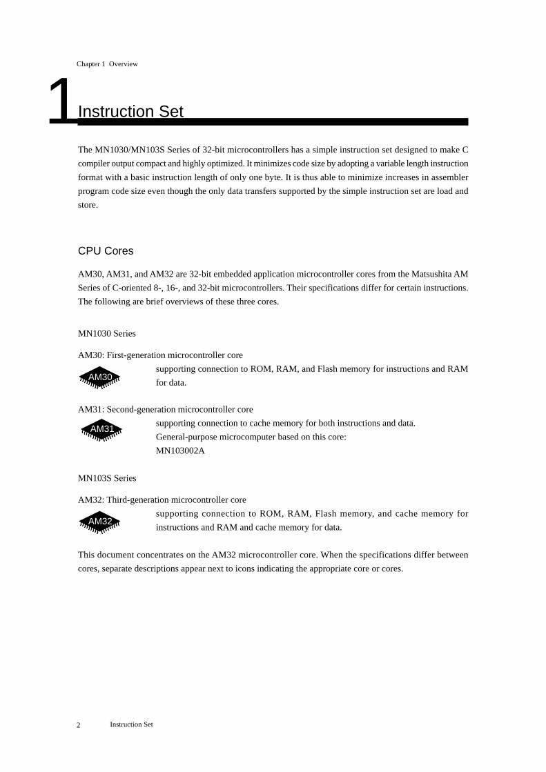
2
Chapter 1 Overview
1Instruction Set
The MN1030/MN103S Series of 32-bit microcontrollers has a simple instruction set designed to make C
compiler output compact and highly optimized. It minimizes code size by adopting a variable length instruction
format with a basic instruction length of only one byte. It is thus able to minimize increases in assembler
program code size even though the only data transfers supported by the simple instruction set are load and
store.
CPU Cores
AM30, AM31, and AM32 are 32-bit embedded application microcontroller cores from the Matsushita AM
Series of C-oriented 8-, 16-, and 32-bit microcontrollers. Their specifications differ for certain instructions.
The following are brief overviews of these three cores.
MN1030 Series
AM30: First-generation microcontroller core
supporting connection to ROM, RAM, and Flash memory for instructions and RAM
for data.
AM31: Second-generation microcontroller core
supporting connection to cache memory for both instructions and data.
General-purpose microcomputer based on this core:
MN103002A
MN103S Series
AM32: Third-generation microcontroller core
supporting connection to ROM, RAM, Flash memory, and cache memory for
instructions and RAM and cache memory for data.
This document concentrates on the AM32 microcontroller core. When the specifications differ between
cores, separate descriptions appear next to icons indicating the appropriate core or cores.
AM30
AM31
AM32
Instruction Set
3
Chapter 1 Overview
Register Set
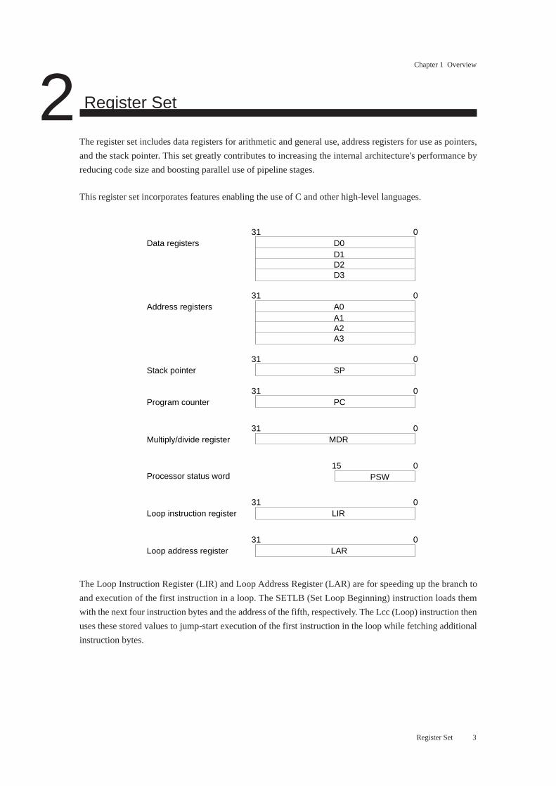
The register set includes data registers for arithmetic and general use, address registers for use as pointers,
and the stack pointer. This set greatly contributes to increasing the internal architecture's performance by
reducing code size and boosting parallel use of pipeline stages.
This register set incorporates features enabling the use of C and other high-level languages.
The Loop Instruction Register (LIR) and Loop Address Register (LAR) are for speeding up the branch to
and execution of the first instruction in a loop. The SETLB (Set Loop Beginning) instruction loads them
with the next four instruction bytes and the address of the fifth, respectively. The Lcc (Loop) instruction then
uses these stored values to jump-start execution of the first instruction in the loop while fetching additional
instruction bytes.
2
Register Set
31D0D1D2D3
0
31A0A1A2A3
0
31SP
0
31PC
0
31MDR
0
15PSW
0
31LIR
0
31LAR
0
Data registers
Address registers
Stack pointer
Program counter
Multiply/divide register
Processor status word
Loop instruction register
Loop address register

4
Chapter 1 Overview
2.1 Data Registers
D0 to D3: Data Registers (32 bits x 4)
These four 32-bit registers are for arithmetic and general use. Data values are automatically zero-extended
to 32 bits when they are loaded from memory. The EXTB and EXTH instructions are also available for sign-
extending them once loaded.
For 8-bit data, a load operation copies the data from memory into the lowest eight bits of the register and
zeros the other bits. A store copies the lowest eight bits of the register to memory. Following the load
operation with an EXTB instruction sign-extends it from 8 bits to 32.
For 16-bit data, a load operation copies the data from memory into the lowest 16 bits of the register and
zeros the other bits. A store copies the lowest 16 bits of the register to memory. Following the load operation
with an EXTH instruction sign-extends it from 16 bits to 32.
2.2 Address Registers
A0 to A3: Address Registers (32 bits x 4)
These four 32-bit registers are for use as address pointers, so support only the operations relevant to address
calculations: addition, subtraction, and comparison.
Because the contents are pointers, transfers to and from memory are always 32 bits wide.
2.3 Stack Pointer
SP: Stack Pointer (32 bits x 1)
This 32-bit pointer indicates the address at the top of the stack.
Because addressing is by the word, the lowest two bits of any value loaded into this register must be '00'--
that is, a multiple of four.
2.4 Program Counter
PC: Program Counter (32 bit x1)
This 32-bit register holds the address of the instruction currently executing.
2.5 Multiply/Divide Register
MDR: Multiply/ Divide Register (32 bits x 1)
This 32-bit register is for use by multiply and divide instructions. After a multiply operation, it holds the top
32 bits of the 64-bit result. After a divide operation, it holds the 32-bit remainder; before, the top 32 bits of
the 64-bit dividend.
Register Set
5
Chapter 1 Overview
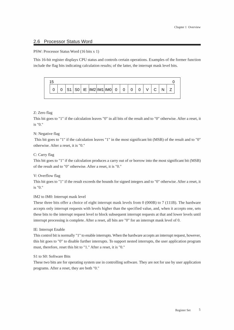
2.6 Processor Status Word
PSW: Processor Status Word (16 bits x 1)
This 16-bit register displays CPU status and controls certain operations. Examples of the former function
include the flag bits indicating calculation results; of the latter, the interrupt mask level bits.
Z: Zero flag
This bit goes to "1" if the calculation leaves "0" in all bits of the result and to "0" otherwise. After a reset, it
is "0."
N: Negative flag
This bit goes to "1" if the calculation leaves "1" in the most significant bit (MSB) of the result and to "0"
otherwise. After a reset, it is "0."
C: Carry flag
This bit goes to "1" if the calculation produces a carry out of or borrow into the most significant bit (MSB)
of the result and to "0" otherwise. After a reset, it is "0."
V: Overflow flag
This bit goes to "1" if the result exceeds the bounds for signed integers and to "0" otherwise. After a reset, it
is "0."
IM2 to IM0: Interrupt mask level
These three bits offer a choice of eight interrupt mask levels from 0 (000B) to 7 (111B). The hardware
accepts only interrupt requests with levels higher than the specified value, and, when it accepts one, sets
these bits to the interrupt request level to block subsequent interrupt requests at that and lower levels until
interrupt processing is complete. After a reset, all bits are "0" for an interrupt mask level of 0.
IE: Interrupt Enable
This control bit is normally "1" to enable interrupts. When the hardware accepts an interrupt request, however,
this bit goes to "0" to disable further interrupts. To support nested interrupts, the user application program
must, therefore, reset this bit to "1." After a reset, it is "0."
S1 to S0: Software Bits
These two bits are for operating system use in controlling software. They are not for use by user application
programs. After a reset, they are both "0."
Register Set
0 0 S1 S0 IE IM2 IM1 IM0 0 0 0 0 V C N Z
015
6
Chapter 1 Overview
2.7 Loop Instruction Register
LIR: Loop Instruction Register (32 bits x 1)
This 32-bit register, used only by the SETLB (Set Loop Beginning) and Lcc (Loop) instructions, holds the
first four instruction bytes of the loop for use in speeding up iterations. The SETLB instruction loads it prior
to the loop, and the Lcc instruction at the end of the loop then executes the copy while the pipeline fetches
more instruction bytes starting from the fifth.
For further details, see the SETLB description in Chapter 2.
2.8 Loop Address Register
LAR: Loop Address Register (32 bit x 1)
This 32-bit register, used only by the SETLB (Set Loop Beginning) and Lcc (Loop) instructions, holds the
address of the fifth instruction byte of the loop.
Register Set
7
Chapter 1 Overview
Instruction Functions
3
Bitwise Logical
Instructions
Instruction Functions
The instruction set has been kept simple so that C compiler output is compact and highly optimized.
The following table shows all instructions divided into functional groups.
Transfer Sign Extension Clear
MOV EXT CLR
MOVBU EXTB
MOVB*1 EXTB
MOVHU EXTH
MOVH*1 EXTHU
MOVM
Addition Subtraction Multiplication Division
ADD SUB MUL DIV
ADDC SUBC MULU DIVU
INC
INC4
Comparison
CMP
Logical Sum Logical Product Inversion Exclusive OR
OR AND NOT XOR
Test Test and Set Test and Clear
BTST BSET BCLR
Shift Rotation
ASR*2 ROR
LSR*2 ROL
ASL
ASL2
Branch Loop Setup Subroutine Call Return
Bcc SETLB CALL RET
Lcc CALLS RETF
JMP JSR*1 RETS
TRAP RTS*1
RTI
No Operation
NOP
Expansion
UDFnn
UDFUnn*1. MOVB, MOVH, and JSR are assembler shorthand for instruction sequences. RTS is an alias for RETS.
*2. The ASR Dn and LSR Dn variants are assembler shorthand for single-bit shifts of the specified register.
The BSET and BCLR instructions temporarily disable interrupts and lock the bus for exclusive
CPU use while they execute.
The BSET and BCLR instructions do not lock the bus for operations on
data in the cachable region of external memory.
Data
Transfer
Instructions
Arithmetic
Instructions
Compare
Instructions
Bit Manipula-
tion Instructions
Shift
Instructions
Branch
Instructions
NOP Instruction
User Defined
Instructions
AM31 AM32
8
Chapter 1 Overview
3.1 Data Transfer Instructions
Data transfer instructions copy data between registers or between a register and memory. They fall into three
groups: MOV, EXT, and CLR.
The MOV group offers a variety of modes for addressing data and provides sign- and zero-extension as
necessary for displacements, immediate values, etc.
The EXT group provides sign- and zero-extension within the specified register or to the Multiply/Divide
Register (MDR).
The CLR instruction sets the specified register to zero.
Instruction Description
MOV Word (32-bit) transfer between registers, word transfer between a register
and memory, or loading of an immediate value into a register
MOVBU Byte transfer between registers with zero-extension for loads
MOVB*1 Byte transfer between registers with sign-extension for loads
MOVHU Half-word (16-bit) transfer between registers with zero-extension for loads
MOVH*1 Half-word (16-bit) transfer between registers with sign-extension for loads
MOVM Multiregister transfer to and from stack in memory
EXT Sign-extension of 32-bit word register into Multiply/Divide Register (MDR)
EXTB Sign-extension of byte to 32 bits
EXTBU Zero-extension of byte to 32 bits
EXTH Sign-extension of half-word to 32 bits
EXTHU Zero-extension of half-word to 32 bits
CLR Register clear
*1. MOVB and MOVH are assembler shorthand for instruction sequences.
3.2 Arithmetic Instructions
Arithmetic instructions perform an arithmetic operation on the two source operands (or one), store the result
in a register, and--except for INC and INC4 with address registers, ADD with the Stack Pointer (SP), etc.--
update the PSW flags according to the result. Because of their frequent use in address calculations, there are
separate instructions for incrementing by 1 and 4.
Instruction Description
Addition Addition with carry
Subtraction Subtraction with carry
Multiplication (signed) Multiplication (unsigned)
Division (signed) Division (unsigned)
Instruction Functions
9
Chapter 1 Overview
3.3 Compare Instructions
The compare instructions subtract an immediate value or the contents of a register from the contents of
another register, setting PSW flags for use in conditional branch instructions.
Instruction Description
CMP Comparison
3.4 Bitwise Logical Instructions
Bitwise logical instructions perform a logical operation on the two source operands (or one), store the result
in a register, and update the PSW flags according to the result.
Instruction Description
AND Logical Product
OR Logical Sum
XOR Exclusive OR
NOT Inversion (ones complement)
3.5 Bit Manipulation Instructions
Bit manipulation instructions perform logical operations on the two source operands--an immediate value
and a register, an immediate value and a memory location, a register and a memory location--and update the
PSW flags according to the result.
Instruction Description
BTST Bit test
BSET Bit test and set (byte)
BCLR Bit test and clear (byte)
3.6 Shift Instructions
Shift instructions shift or rotate the specified register by the specified (or implied) amount and update the
PSW flags according to the result.
Instruction Description
ASR*2 Arithmetic shift right
LSR*2 Logical shift right
ASL Arithmetic shift left
ASL2 Arithmetic 2-bit shift left
ROR Single-bit rotation right
ROL Single-bit rotation left
*2. The ASR Dn and LSR Dn variants are assembler shorthand for single-bit shifts of the specified register.
Instruction Functions
10
Chapter 1 Overview
3.7 Branch Instructions
Branch instructions change the flow of execution. In addition to the usual conditional branch (Bcc) instruc-
tion, there is a separate variant (Lcc) for use in loops. The latter relies on special registers to reduce the
penalty normally associated with taking the branch and thus speed up loop execution. The subroutine call
and return instructions feature high-performance specifications that automatically take care of manipulating
the Program Counter (PC), saving the appropriate registers to and restoring them from the stack, and secur-
ing and releasing the necessary stack space.
Instruction Description
Bcc Conditional branch (relative to PC)
Lcc Loop conditional branch (relative to PC)
SETLB Loop setup
JMP Unconditional branch (relative to PC or register indirect)
CALL Subroutine call (high-performance variant)
CALLS Subroutine call
RET Return from subroutine (high-performance variant)
RETF Return from subroutine (high-performance, high-speed variant)
RETS Return from subroutine
JSR*3 Subroutine call
RTS*3 Return from subroutine
RTI Return from interrupt handler
TRAP Subroutine call to predetermined address*3. JSR is assembler shorthand for an instruction sequence.
*4. RTS is an alias for RETS.
3.8 NOP Instruction
The NOP instruction does nothing but consume one cycle. It does not affect any resources.
Instruction Description
NOP No Operation
3.9 User Defined Instructions
User defined instructions access add-on expansion units. They have a fixed format and reserved positions in
the instruction mapping. For further details, refer to the documentation for the particular device.
Instruction Description
UDFnn User defined instruction (with sign extension)
UDFUnn User defined instruction (with zero extension)
Instruction Functions
11
Chapter 1 Overview
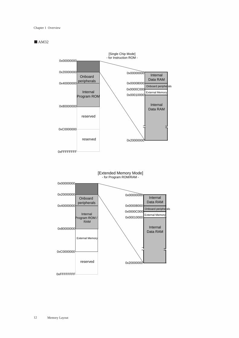
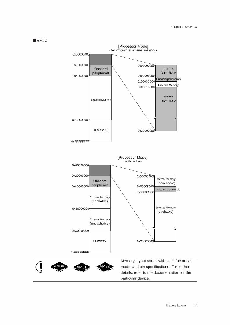
Memory Layout
The MN1030/MN103S Series of 32-bit microcontrollers has a 4-gigabyte linear address space. Memory
assignments within this address space follow the patterns below. Note how the memory map varies with
such factors as internal memory configuration and memory mode. One assignment that is common throughout,
however, is the location of the reset vector. It is always at 0x40000000.
■ AM30
■ AM31
4
InternalData RAM
InternalInstruction
ROM
reserved
reserved
0x00000000
0x20000000
0x40000000
0x80000000
0xC0000000
0xFFFFFFFF
[Single chip mode]- For instruction ROM -
Onboardinperipherals
reserved
0x00000000
0xC0000000
0xFFFFFFFF
[Expansion Memory Mode]- For Instruction ROM/RAM -
External �memory
0x20000000
0x40000000
0x80000000
Internal�Data RAM
Internal�Instruction RAM�Instruction ROM
Internal �peripherals
InternalData RAM
Internalperipherals
reserved
0x00000000
0x20000000
0x40000000
0xC0000000
0xFFFFFFFF
[Processor mode]- For Instruction ROM/RAM -
ExternalMemory
External memory�
(cachable)
reserved
0x00000000
0x20000000
0x40000000
0x80000000
0xC0000000
0xFFFFFFFF
[Processor mode]- For Cache -
External memory�
(uncachable)
�
External memory�
(cachable)
Onboard�peripherals�
(uncachable)
Memory Layout
12
Chapter 1 Overview
■ AM32
Onboardperipherals
InternalProgram ROM
reserved
reserved
0x00000000
0x20000000
0x40000000
0x80000000
0xC0000000
0xFFFFFFFF
[Single Chip Mode]- for Instruction ROM -
0x00000000
0x00008000
0x0000C000
0x00010000
0x20000000
~~ ~~
InternalData RAM
Onboard peripherals
External Memory
InternalData RAM
0x00000000
0x20000000
0x40000000
0x80000000
0xC0000000
0xFFFFFFFF
[Extended Memory Mode]- for Program ROM/RAM -
0x00000000
0x00008000
0x0000C000
0x00010000
0x20000000
~ ~~
InternalData RAM
Onboard peripherals
External Memory
InternalData RAM
Onboard peripherals
InternalProgram ROM /
RAM
External Memory
reserved
~
Memory Layout
13
Chapter 1 Overview
■ AM32
Memory layout varies with such factors as
model and pin specifications. For further
details, refer to the documentation for the
particular device.
0x00000000
0x20000000
0x40000000
0xC0000000
0xFFFFFFFF
[Processor Mode]- for Program in external memory -
Onboardperipherals
reserved
External Memory
0x00000000
0x00008000
0x0000C000
0x00010000
0x20000000
~~ ~~
InternalData RAM
Onboard peripherals
External Memory
InternalData RAM
0x00000000
0x20000000
0x40000000
0x80000000
0xC0000000
0xFFFFFFFF
[Processor Mode]- with cache -
External Memory
(uncachable)
External Memory
(cachable)
Onboardperipherals
reserved
0x00000000
0x00008000
0x0000C000
0x20000000
~~ ~~
External memory
(uncachable)
Onboard peripherals
External Memory
(cachable)
AM30 AM31 AM32
Memory Layout
14
Chapter 1 Overview
Addressing Modes
The addressing modes available consist of the following six most heavily used by C compilers.
1. Register direct
2. Immediate value
3. Register indirect
4. Register relative indirect
5. Absolute
6. Register indirect with indexing
Data transfer instructions offer all six addressing modes: register direct, immediate, register indirect, register
relative indirect, absolute, and register indirect with indexing.
Register arithmetic instructions offer only two addressing modes: register direct and absolute.
Register indirect addressing with indexing is for more efficient access to arrays and the like.
5
Addressing Mode
15
Chapter 1 Overview
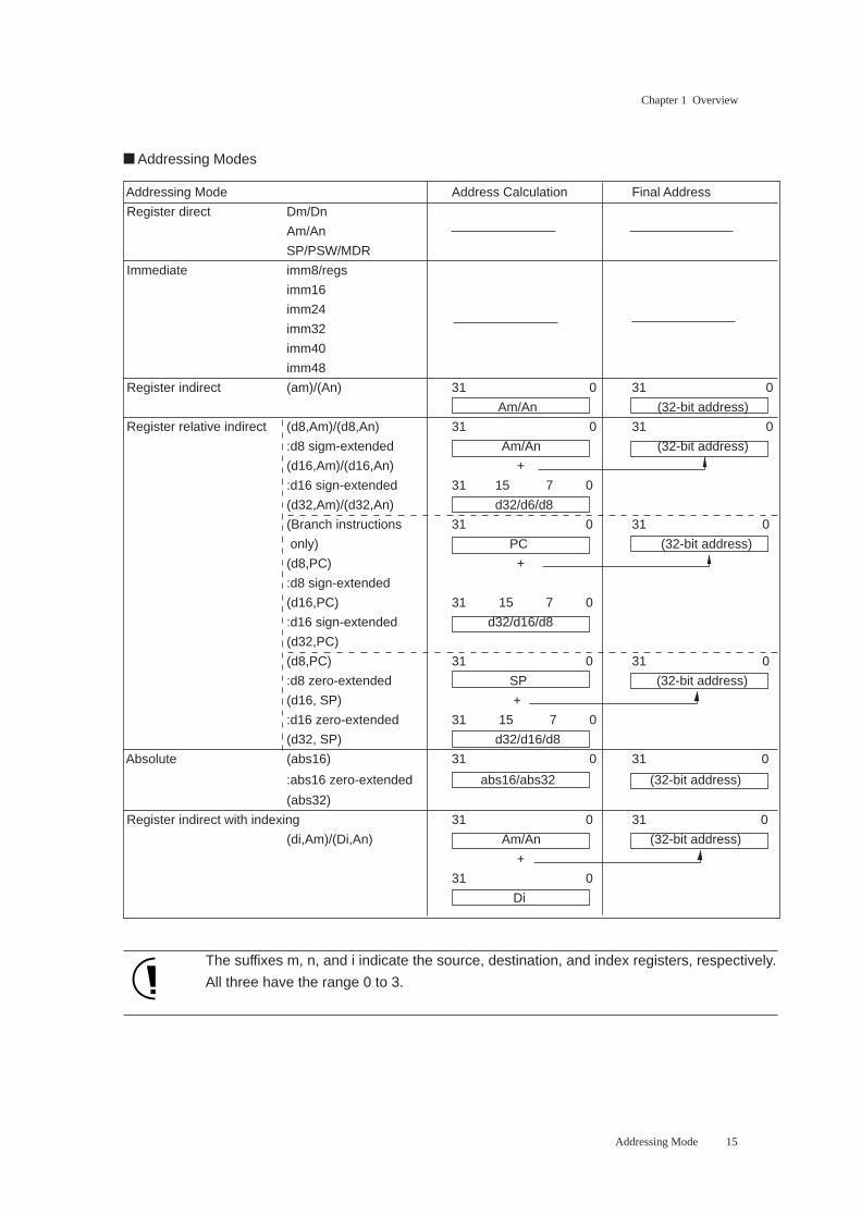
■ Addressing Modes
Addressing Mode Address Calculation Final Address
Register direct Dm/Dn
Am/An
SP/PSW/MDR
Immediate imm8/regs
imm16
imm24
imm32
imm40
imm48
Register indirect (am)/(An) 31 0 31 0
Am/An (32-bit address)
Register relative indirect (d8,Am)/(d8,An) 31 0 31 0
:d8 sigm-extended Am/An (32-bit address)
(d16,Am)/(d16,An) +
:d16 sign-extended 31 15 7 0
(d32,Am)/(d32,An) d32/d6/d8
(Branch instructions 31 0 31 0
only) PC (32-bit address)
(d8,PC) +
:d8 sign-extended
(d16,PC) 31 15 7 0
:d16 sign-extended d32/d16/d8
(d32,PC)
(d8,PC) 31 0 31 0
:d8 zero-extended SP (32-bit address)
(d16, SP) +
:d16 zero-extended 31 15 7 0
(d32, SP) d32/d16/d8
Absolute (abs16) 31 0 31 0
:abs16 zero-extended abs16/abs32 (32-bit address)
(abs32)
Register indirect with indexing 31 0 31 0
(di,Am)/(Di,An) Am/An (32-bit address)
+
31 0
Di
The suffixes m, n, and i indicate the source, destination, and index registers, respectively.
All three have the range 0 to 3.
Addressing Mode
16
Chapter 1 Overview
5.1 Register Direct Addressing
Register direct addressing specifies an operand as the name of a register from the following list.
Dn/Dm (32-bit) Data register
An/Am (32-bit) Address register
SP (32-bit) Stack Pointer
PSW (16-bit) Processor Status Word
MDR (32-bit) Multiply/Divide Register
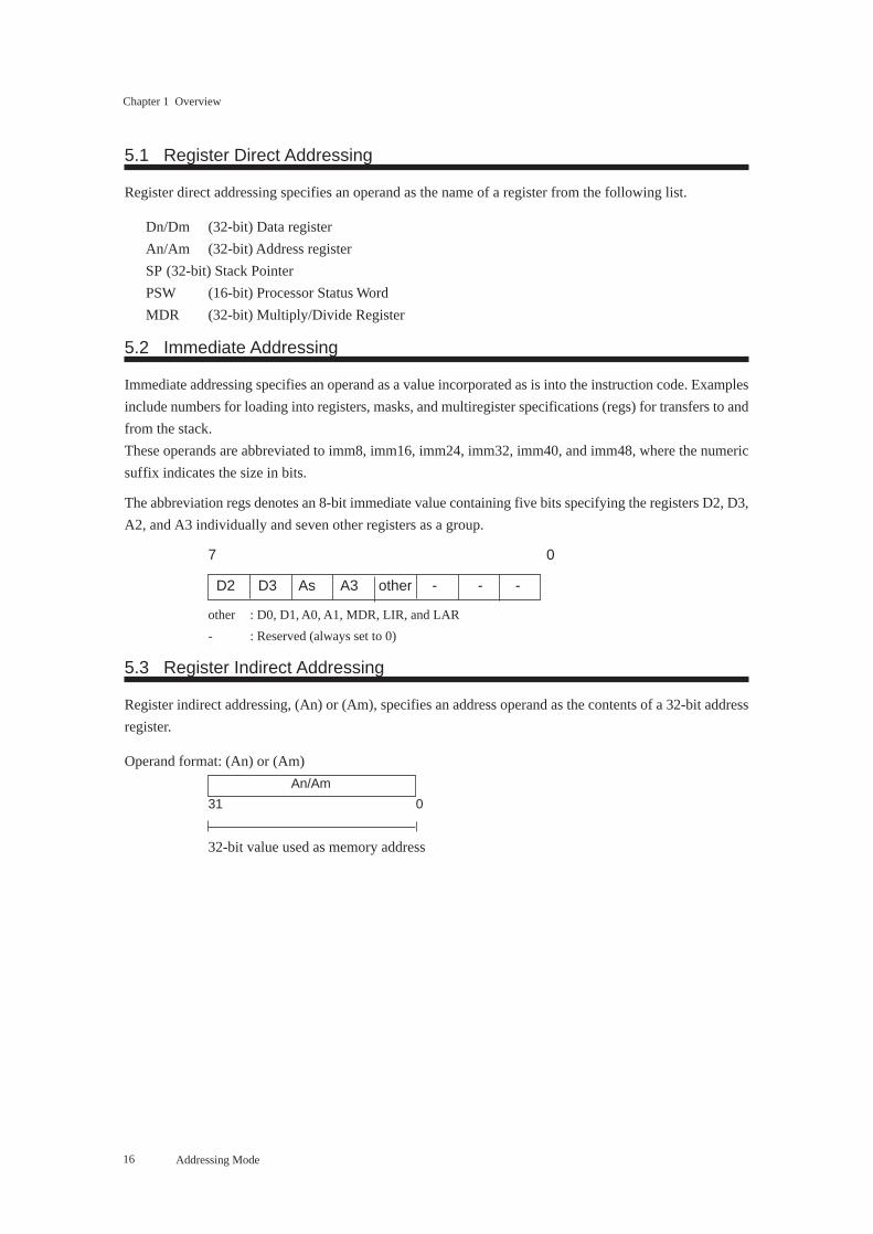
5.2 Immediate Addressing
Immediate addressing specifies an operand as a value incorporated as is into the instruction code. Examples
include numbers for loading into registers, masks, and multiregister specifications (regs) for transfers to and
from the stack.
These operands are abbreviated to imm8, imm16, imm24, imm32, imm40, and imm48, where the numeric
suffix indicates the size in bits.
The abbreviation regs denotes an 8-bit immediate value containing five bits specifying the registers D2, D3,
A2, and A3 individually and seven other registers as a group.
7 0
D2 D3 As A3 other - - -
other : D0, D1, A0, A1, MDR, LIR, and LAR
- : Reserved (always set to 0)
5.3 Register Indirect Addressing
Register indirect addressing, (An) or (Am), specifies an address operand as the contents of a 32-bit address
register.
Operand format: (An) or (Am)
An/Am
31 0
32-bit value used as memory address
Addressing Mode
17
Chapter 1 Overview
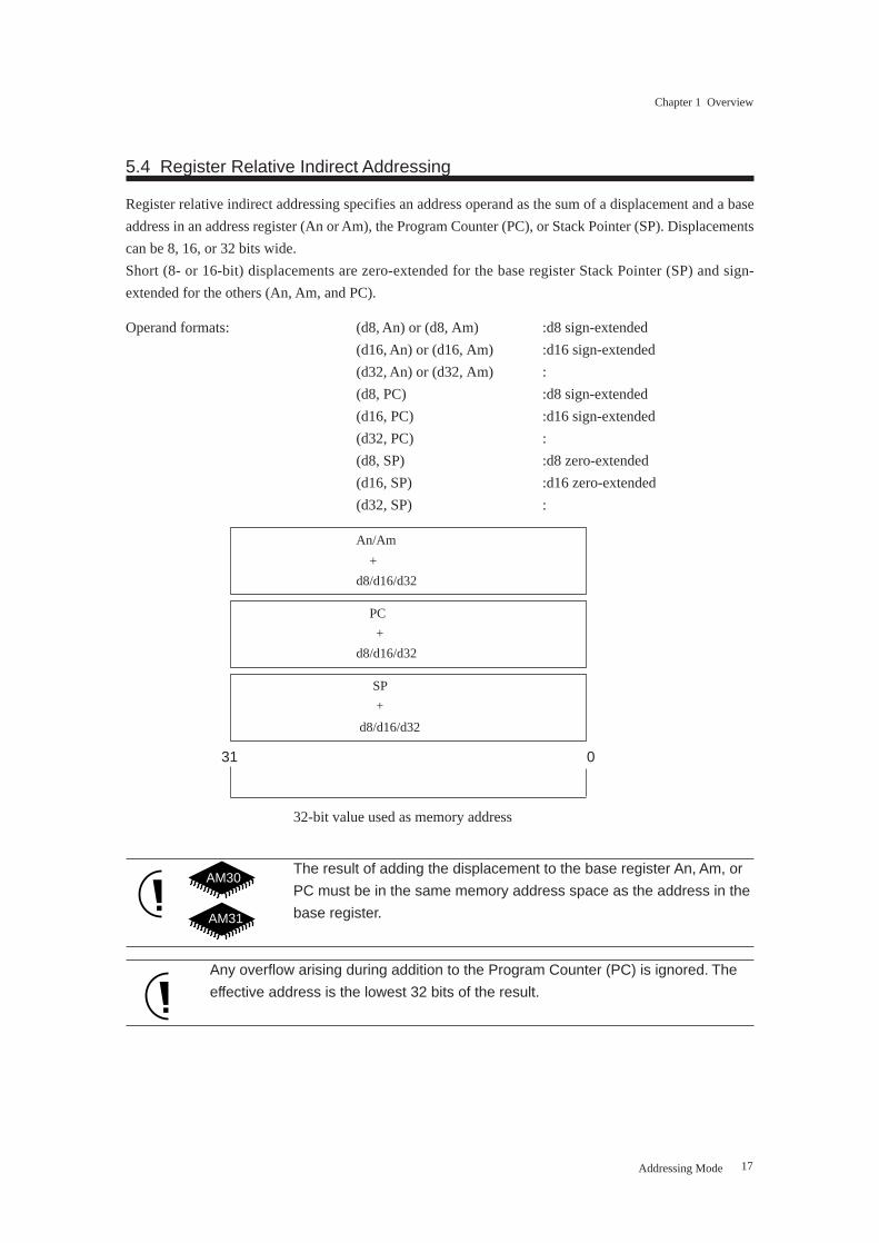
5.4 Register Relative Indirect Addressing
Register relative indirect addressing specifies an address operand as the sum of a displacement and a base
address in an address register (An or Am), the Program Counter (PC), or Stack Pointer (SP). Displacements
can be 8, 16, or 32 bits wide.
Short (8- or 16-bit) displacements are zero-extended for the base register Stack Pointer (SP) and sign-
extended for the others (An, Am, and PC).
Operand formats: (d8, An) or (d8, Am) :d8 sign-extended
(d16, An) or (d16, Am) :d16 sign-extended
(d32, An) or (d32, Am) :
(d8, PC) :d8 sign-extended
(d16, PC) :d16 sign-extended
(d32, PC) :
(d8, SP) :d8 zero-extended
(d16, SP) :d16 zero-extended
(d32, SP) :
An/Am
+
d8/d16/d32
PC
+
d8/d16/d32
SP
+
d8/d16/d32
31 0
32-bit value used as memory address
The result of adding the displacement to the base register An, Am, or
PC must be in the same memory address space as the address in the
base register.
Any overflow arising during addition to the Program Counter (PC) is ignored. The
effective address is the lowest 32 bits of the result.
Addressing Mode
AM30
AM31
18
Chapter 1 Overview
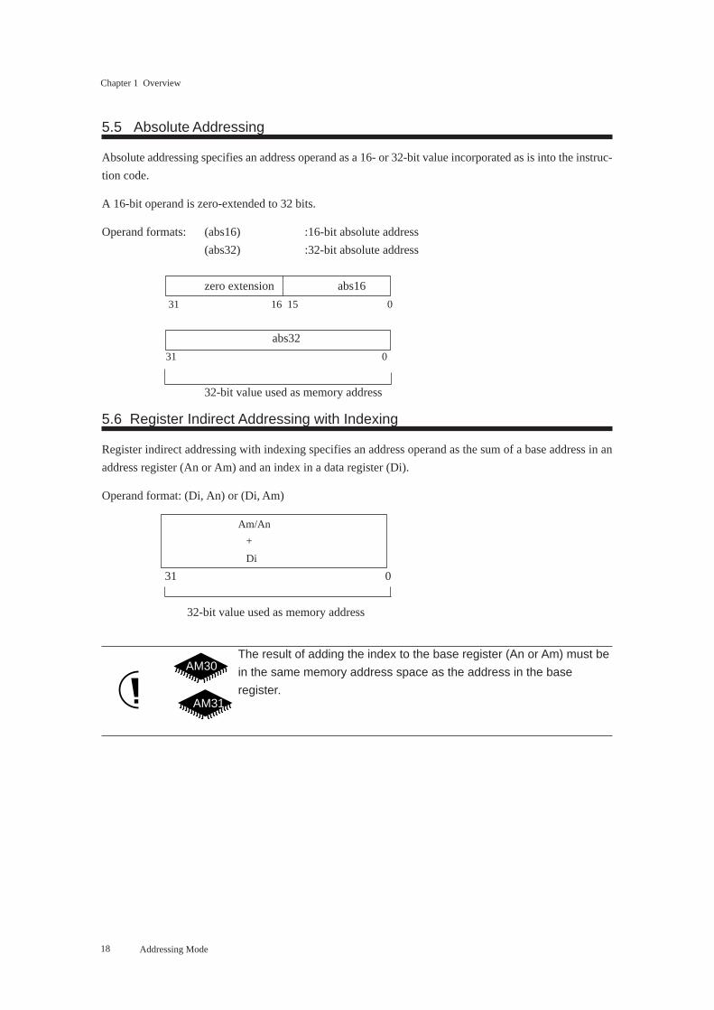
5.5 Absolute Addressing
Absolute addressing specifies an address operand as a 16- or 32-bit value incorporated as is into the instruc-
tion code.
A 16-bit operand is zero-extended to 32 bits.
Operand formats: (abs16) :16-bit absolute address
(abs32) :32-bit absolute address
zero extension abs16
31 16 15 0
abs32
31 0
32-bit value used as memory address
5.6 Register Indirect Addressing with Indexing
Register indirect addressing with indexing specifies an address operand as the sum of a base address in an
address register (An or Am) and an index in a data register (Di).
Operand format: (Di, An) or (Di, Am)
Am/An
+
Di
31 0
32-bit value used as memory address
The result of adding the index to the base register (An or Am) must be
in the same memory address space as the address in the base
register.
Addressing Mode
AM30
AM31
19
Chapter 1 Overview
Instruction Formats
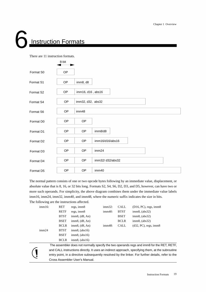
There are 11 instruction formats.
The normal pattern consists of one or two opcode bytes following by an immediate value, displacement, or
absolute value that is 8, 16, or 32 bits long. Formats S2, S4, S6, D2, D3, and D5, however, can have two or
more such operands. For simplicity, the above diagram combines them under the immediate value labels
imm16, imm24, imm32, imm40, and imm48, where the numeric suffix indicates the size in bits.
The following are the instructions affected.imm16: RET regs, imm8 imm32: CALL (D16, PC), regs, imm8
RETF regs, imm8 imm40: BTST imm8, (abs32)
BTST imm8, (d8, An) BSET imm8, (abs32)
BSET imm8, (d8, An) BCLR imm8, (abs32)
BCLR imm8, (d8, An) imm48: CALL (d32, PC), regs, imm8
imm24 BTST imm8, (abs16)
BSET imm8, (abs16)
BCLR imm8, (abs16)
The assembler does not normally specify the two operands regs and imm8 for the RET, RETF,
and CALL instructions directly. It uses an indirect approach, specifying them, at the subroutine
entry point, in a directive subsequently resolved by the linker. For further details, refer to the
Cross Assembler User's Manual.
Instruction Formats
6OP
OP
OP
OP
OP
OP
OP
OP
OP
OP
OP
OP
OP
imm8, d8
imm16, d16 , abs16
imm32, d32, abs32
imm48
imm8/d8
imm16/d16/abs16
imm24
8-bit
Format S0
Format S1
Format S2
Format S4
Format S6
Format D0
Format D2
Format D1
Format D3
Format D4
OP OP imm40Format D5
OP OP imm32/ d32/abs32
20
Chapter 1 Overview
Instruction Formats
6.1 Data Formats
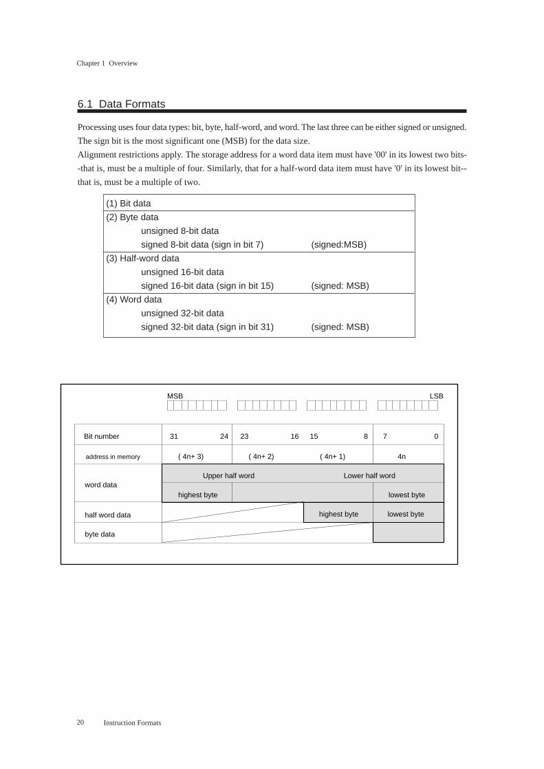
Processing uses four data types: bit, byte, half-word, and word. The last three can be either signed or unsigned.
The sign bit is the most significant one (MSB) for the data size.
Alignment restrictions apply. The storage address for a word data item must have '00' in its lowest two bits-
-that is, must be a multiple of four. Similarly, that for a half-word data item must have '0' in its lowest bit--
that is, must be a multiple of two.
(1) Bit data
(2) Byte data
unsigned 8-bit data
signed 8-bit data (sign in bit 7) (signed:MSB)
(3) Half-word data
unsigned 16-bit data
signed 16-bit data (sign in bit 15) (signed: MSB)
(4) Word data
unsigned 32-bit data
signed 32-bit data (sign in bit 31) (signed: MSB)
MSB LSB
address in memory
word data
Bit number 31 24 23 16 15 8 7 0
4n ( 4n+ 1)( 4n+ 2)( 4n+ 3)
highest byte lowest byte
Upper half word Lower half word
half word data highest byte lowest byte
byte data
21
Chapter 1 Overview
Addressing Mode
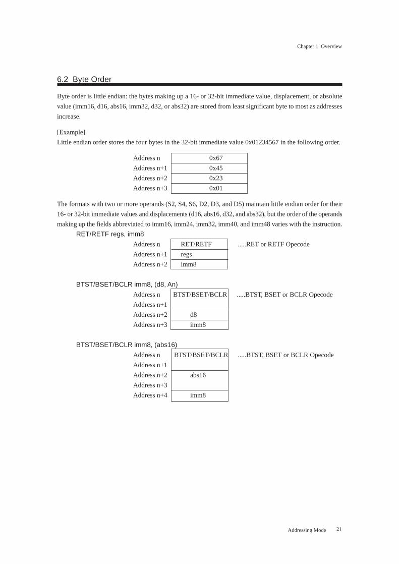
6.2 Byte Order
Byte order is little endian: the bytes making up a 16- or 32-bit immediate value, displacement, or absolute
value (imm16, d16, abs16, imm32, d32, or abs32) are stored from least significant byte to most as addresses
increase.
[Example]
Little endian order stores the four bytes in the 32-bit immediate value 0x01234567 in the following order.
Address n 0x67
Address n+1 0x45
Address n+2 0x23
Address n+3 0x01
The formats with two or more operands (S2, S4, S6, D2, D3, and D5) maintain little endian order for their
16- or 32-bit immediate values and displacements (d16, abs16, d32, and abs32), but the order of the operands
making up the fields abbreviated to imm16, imm24, imm32, imm40, and imm48 varies with the instruction.
RET/RETF regs, imm8
Address n RET/RETF .....RET or RETF Opecode
Address n+1 regs
Address n+2 imm8
BTST/BSET/BCLR imm8, (d8, An)
Address n BTST/BSET/BCLR .....BTST, BSET or BCLR Opecode
Address n+1
Address n+2 d8
Address n+3 imm8
BTST/BSET/BCLR imm8, (abs16)
Address n BTST/BSET/BCLR .....BTST, BSET or BCLR Opecode
Address n+1
Address n+2 abs16
Address n+3
Address n+4 imm8
22
Chapter 1 Overview
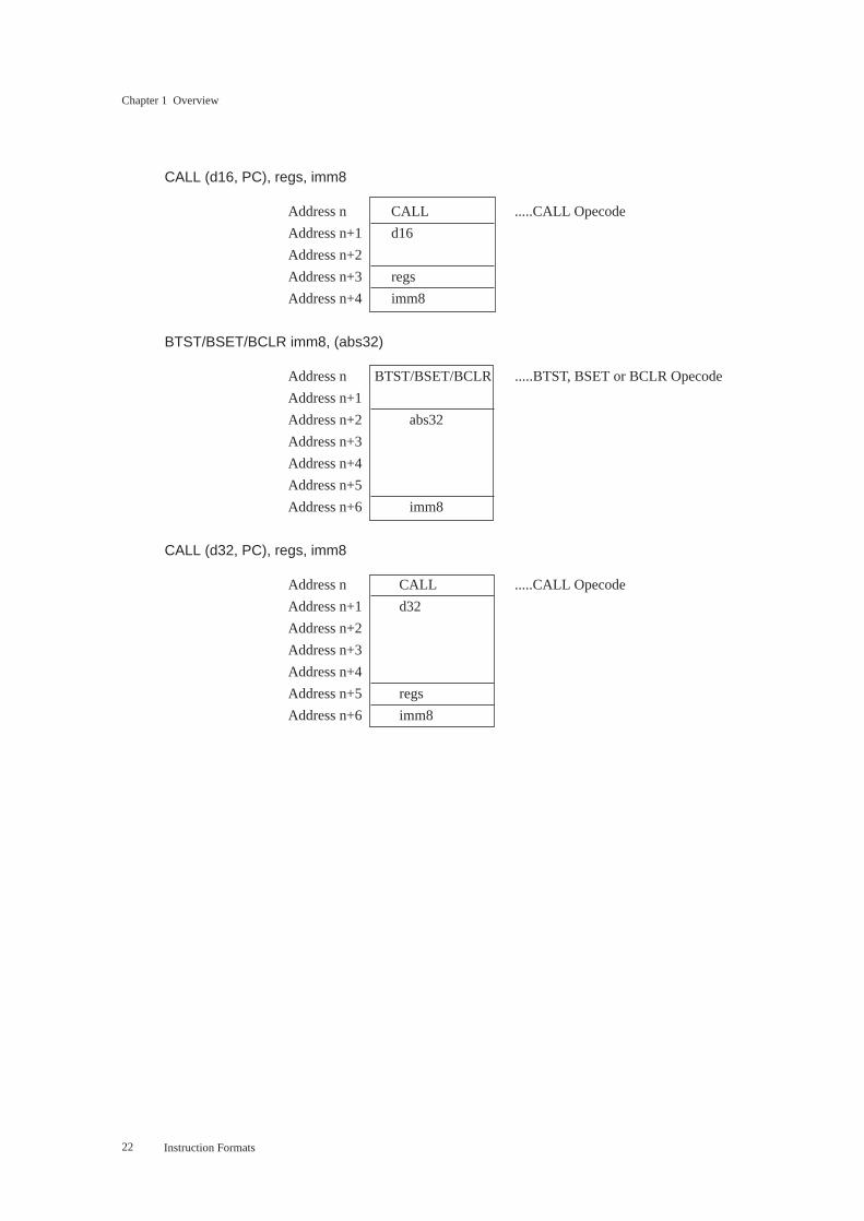
CALL (d16, PC), regs, imm8
Address n CALL .....CALL Opecode
Address n+1 d16
Address n+2
Address n+3 regs
Address n+4 imm8
BTST/BSET/BCLR imm8, (abs32)
Address n BTST/BSET/BCLR .....BTST, BSET or BCLR Opecode
Address n+1
Address n+2 abs32
Address n+3
Address n+4
Address n+5
Address n+6 imm8
CALL (d32, PC), regs, imm8
Address n CALL .....CALL Opecode
Address n+1 d32
Address n+2
Address n+3
Address n+4
Address n+5 regs
Address n+6 imm8
Instruction Formats

Instruction Specifications 2
Chapter 2 Instruction Specifications
24
Symbol Definitions
■ Following is the list of symbols used in the instruction specifications.
Reg :register (used for general meaning)
Am, An :address register (m, n=3 to 0)
Dm, Dn,Di :data register (m, n, i=3 to 0)
MDR :multiply/divide register
PSW :processor status word
PC :program counter
SP :stack pointer
LIR :loop instruction register
LAR :loop address register
{MDR,Dn} :64-bit data defined whose upper 32-bit in MDR and lower 32-bit in register Dn within a "{ }".
Mem :memory (used for general meaning)
imm :immediate value (used for general meaning)
imm8 :8-bit immediate value
imm16 :16-bit immediate value
imm32 :32-bit immediate value
d8 :8-bit displacement
d16 :16-bit displacement
d32 :32-bit displacement
abs16 :16-bit absolute
abs32 :32-bit absolute
( ) :indirect addressing
Refer to "Chapter 1 section 5, Addressing Mode" for details.
regs :multiple registers specification
0x . . . . :hexadecimal notation(the numbers following 0x are expressed in hexadecimal notation.)
.bpn :bit location ("n" means location of bit; 0 to 31)
.lsb :bit location (bit 0)
.msb :bit location (bit 31)
& :logical AND
| :logical OR
^ :exclusive OR
~ :bit inverted
<<n :n-bit shift left
>>n :n-bit shift right
→ :move
: :reflection of operation result
(sign_ext) :sign-extend
(zero_ext) :zero-extend
label :address
VF :overflow flag
CF :carry flag
NF :nagative flag
ZF :zero flag
temp :temporary register
Explanation of Notations
Chapter 2 Instruction Specifications
25
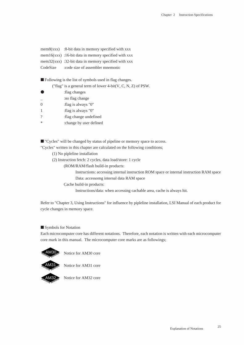
mem8(xxx) :8-bit data in memory specified with xxx
mem16(xxx) :16-bit data in memory specified with xxx
mem32(xxx) :32-bit data in memory specified with xxx
CodeSize :code size of assembler mnemonic
■ Following is the list of symbols used in flag changes.
("flag" is a general term of lower 4-bit(V, C, N, Z) of PSW.
● :flag changes
_ :no flag change
0 :flag is always "0"
1 :flag is always "0"
? :flag change undefined
* :change by user defined
■ "Cycles" will be changed by status of pipeline or memory space to access.
"Cycles" written in this chapter are calculated on the following conditions;
(1) No pipleline installation
(2) Instruction fetch: 2 cycles, data load/store: 1 cycle
(ROM/RAM/flash build-in products:
Instructions: accessing internal instruction ROM space or internal instruction RAM space
Data: accessomg internal data RAM space
Cache build-in products:
Instructions/data: when accessing cachable area, cache is always hit.
Refer to "Chapter 3, Using Instructions" for influence by pipleline installation, LSI Manual of each product for
cycle changes in memory space.
■ Symbols for Notation
Each microcomputer core has different notations. Therefore, each notation is written with each microcomputer
core mark in this manual. The microcomputer core marks are as followings;
Notice for AM30 core
Notice for AM31 core
Notice for AM32 core
Explanation of Notations
AM30
AM31
AM32
Chapter 2 Instruction Specifications
26
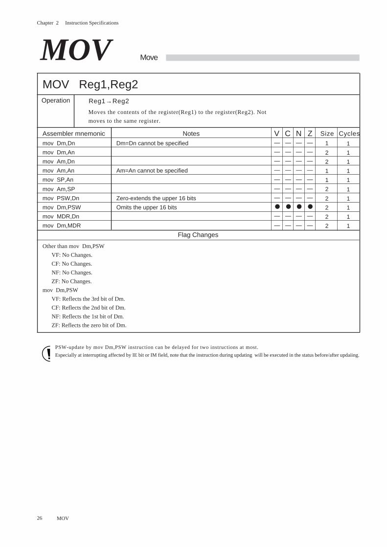
MOV Move
MOV Reg1,Reg2
V C Z
Operation
Assembler mnemonic
Reg1→Reg2
Moves the contents of the register(Reg1) to the register(Reg2). Not
moves to the same register.
Size Cycles
mov Dm,Dn Dm=Dn cannot be specified
mov Dm,An
mov Am,Dn
mov Am,An Am=An cannot be specified
mov SP,An
mov Am,SP
mov PSW,Dn Zero-extends the upper 16 bits
mov Dm,PSW Omits the upper 16 bits
mov MDR,Dn
mov Dm,MDR
Notes
Flag Changes
Other than mov Dm,PSW
VF: No Changes.
CF: No Changes.
NF: No Changes.
ZF: No Changes.
mov Dm,PSW
VF: Reflects the 3rd bit of Dm.
CF: Reflects the 2nd bit of Dm.
NF: Reflects the 1st bit of Dm.
ZF: Reflects the zero bit of Dm.
N
PSW-update by mov Dm,PSW instruction can be delayed for two instructions at most.
Especially at interrupting affected by IE bit or IM field, note that the instruction during updating will be executed in the status before/after updaiing.
1
2
2
1
1
2
2
2
2
2
1
1
1
1
1
1
1
1
1
1
MOV
—
—
—
—
—
—
—
●
—
—
—
—
—
—
—
—
—
●
—
—
—
—
—
—
—
—
—
●
—
—
—
—
—
—
—
—
—
●
—
—
Chapter 2 Instruction Specifications
27
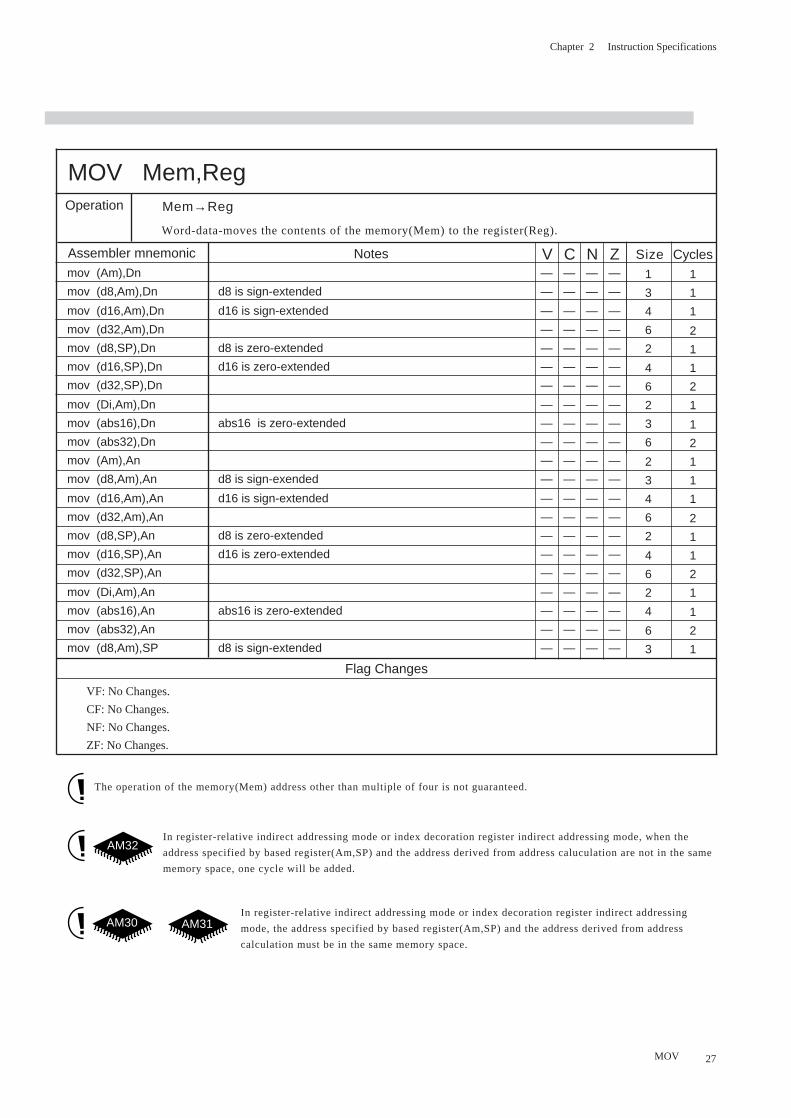
MOV Mem,RegOperation
Assembler mnemonic
Mem→Reg
Word-data-moves the contents of the memory(Mem) to the register(Reg).
Size Cyclesmov (Am),Dn
mov (d8,Am),Dn d8 is sign-extended
mov (d16,Am),Dn d16 is sign-extended
mov (d32,Am),Dn
mov (d8,SP),Dn d8 is zero-extended
mov (d16,SP),Dn d16 is zero-extended
mov (d32,SP),Dn
mov (Di,Am),Dn
mov (abs16),Dn abs16 is zero-extended
mov (abs32),Dn
mov (Am),An
mov (d8,Am),An d8 is sign-exended
mov (d16,Am),An d16 is sign-extended
mov (d32,Am),An
mov (d8,SP),An d8 is zero-extended
mov (d16,SP),An d16 is zero-extended
mov (d32,SP),An
mov (Di,Am),An
mov (abs16),An abs16 is zero-extended
mov (abs32),An
mov (d8,Am),SP d8 is sign-extended
Notes
Flag Changes
VF: No Changes.
CF: No Changes.
NF: No Changes.
ZF: No Changes.
The operation of the memory(Mem) address other than multiple of four is not guaranteed.
1
3
4
6
2
4
6
2
3
6
2
3
4
6
2
4
6
2
4
6
3
1
1
1
2
1
1
2
1
1
2
1
1
1
2
1
1
2
1
1
2
1
MOV
V C ZN—
—
—
—
—
—
—
—
—
—
—
—
—
—
—
—
—
—
—
—
—
—
—
—
—
—
—
—
—
—
—
—
—
—
—
—
—
—
—
—
—
—
—
—
—
—
—
—
—
—
—
—
—
—
—
—
—
—
—
—
—
—
—
—
—
—
—
—
—
—
—
—
—
—
—
—
—
—
—
—
—
—
—
—
In register-relative indirect addressing mode or index decoration register indirect addressing
mode, the address specified by based register(Am,SP) and the address derived from address
calculation must be in the same memory space.
AM30 AM31
In register-relative indirect addressing mode or index decoration register indirect addressing mode, when the
address specified by based register(Am,SP) and the address derived from address caluculation are not in the same
memory space, one cycle will be added.
AM32
Mov
e
Inst
ruct
ions
Chapter 2 Instruction Specifications
28
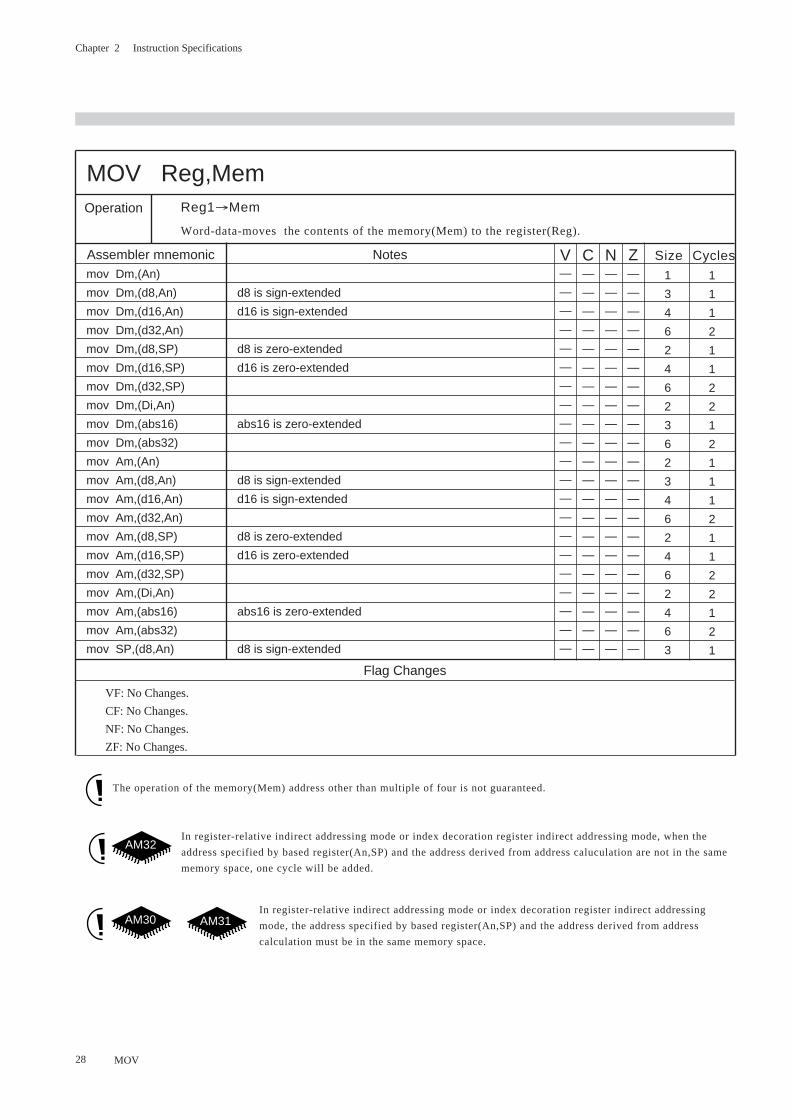
MOV Reg,MemOperation
Assembler mnemonic
Reg1→Mem
Word-data-moves the contents of the memory(Mem) to the register(Reg).
Size Cyclesmov Dm,(An)
mov Dm,(d8,An) d8 is sign-extended
mov Dm,(d16,An) d16 is sign-extended
mov Dm,(d32,An)
mov Dm,(d8,SP) d8 is zero-extended
mov Dm,(d16,SP) d16 is zero-extended
mov Dm,(d32,SP)
mov Dm,(Di,An)
mov Dm,(abs16) abs16 is zero-extended
mov Dm,(abs32)
mov Am,(An)
mov Am,(d8,An) d8 is sign-extended
mov Am,(d16,An) d16 is sign-extended
mov Am,(d32,An)
mov Am,(d8,SP) d8 is zero-extended
mov Am,(d16,SP) d16 is zero-extended
mov Am,(d32,SP)
mov Am,(Di,An)
mov Am,(abs16) abs16 is zero-extended
mov Am,(abs32)
mov SP,(d8,An) d8 is sign-extended
Notes
Flag Changes
VF: No Changes.
CF: No Changes.
NF: No Changes.
ZF: No Changes.
The operation of the memory(Mem) address other than multiple of four is not guaranteed.
1
3
4
6
2
4
6
2
3
6
2
3
4
6
2
4
6
2
4
6
3
1
1
1
2
1
1
2
2
1
2
1
1
1
2
1
1
2
2
1
2
1
MOV
V C ZN—
—
—
—
—
—
—
—
—
—
—
—
—
—
—
—
—
—
—
—
—
—
—
—
—
—
—
—
—
—
—
—
—
—
—
—
—
—
—
—
—
—
—
—
—
—
—
—
—
—
—
—
—
—
—
—
—
—
—
—
—
—
—
—
—
—
—
—
—
—
—
—
—
—
—
—
—
—
—
—
—
—
—
—
In register-relative indirect addressing mode or index decoration register indirect addressing
mode, the address specified by based register(An,SP) and the address derived from address
calculation must be in the same memory space.
AM30 AM31
In register-relative indirect addressing mode or index decoration register indirect addressing mode, when the
address specified by based register(An,SP) and the address derived from address caluculation are not in the same
memory space, one cycle will be added.
AM32
Chapter 2 Instruction Specifications
29
MOV imm,RegOperation
Assembler mnemonic
imm→RegMoves the contents of the immediate value(imm) to the register(Reg).
Size Cyclesmov imm8,Dn imm8 issign-extended
mov imm16,Dn imm16 is sign-extended
mov imm32,Dn
mov imm8,An imm8 is zero-extended
mov imm16,An imm16 is zero-extended
mov imm32,An
Notes
Flag Changes
VF: No Changes.
CF: No Changes.
NF: No Changes.
ZF: No Changes.
2
3
6
2
3
6
1
1
2
1
1
2
MOV
V C ZN—
—
—
—
—
—
—
—
—
—
—
—
—
—
—
—
—
—
—
—
—
—
—
—
Chapter 2 Instruction Specifications
30
MOVBU Zero-extend Byte Move
MOVBU Mem,RegOperation Mem→Reg
Byte-data-moves the contents of the memory(Mem) to the register(Reg)
(8 bits→32 bits; zero-extended)
Assembler mnemonic Size Cycles
movbu (Am),Dn
movbu (d8,Am),Dn d8 is sign-extended
movbu (d16,Am),Dn d16 is sign-extended
movbu (d32,Am),Dn
movbu (d8,SP),Dn d8 is zero-extended
movbu (d16,SP),Dn d16 zero-extended
movbu (d32,SP),Dn
movbu (Di,Am),Dn
movbu (abs16),Dn abs16 zero-extended
movbu (abs32),Dn
Notes
Flag Changes
VF: No Changes.
CF: No Changes.
NF: No Changes.
ZF: No Changes.
2
3
4
6
3
4
6
2
3
6
1
1
1
2
1
1
2
1
1
2
MOVBU
V C ZN—
—
—
—
—
—
—
—
—
—
—
—
—
—
—
—
—
—
—
—
—
—
—
—
—
—
—
—
—
—
—
—
—
—
—
—
—
—
—
—
In register-relative indirect addressing mode or index decoration register indirect addressing
mode, the address specified by based register(Am,SP) and the address derived from address
calculation must be in the same memory space.
AM30 AM31
In register-relative indirect addressing mode or index decoration register indirect addressing mode, when the
address specified by based register(Am,SP) and the address derived from address caluculation are not in the same
memory space, one cycle will be added.
AM32
Chapter 2 Instruction Specifications
31
MOVBU Reg,MemOperation
Assembler mnemonic
Reg→Mem
Byte-moves the contents of the register(Reg) to the memory(Mem).
(32 bits→8bits: Omit the upper)
Size Cycles
movbu Dm,(An)
movbu Dm,(d8,An) d8 is sign-extended
movbu Dm,(d16,An) d16 is sign-extended
movbu Dm,(d32,An)
movbu Dm,(d8,SP) d8 is zero-extended
movbu Dm,(d16,SP) d16 zero-extended
movbu Dm,(d32,SP)
movbu Dm,(Di,An)
movbu Dm,(abs16) abs16 zero-extended
movbu Dm,(abs32)
Notes
Flag Changes
VF: No Changes.
CF: No Changes.
NF: No Changes.
ZF: No Changes.
2
3
4
6
3
4
6
2
3
6
1
1
1
2
1
1
2
2
1
2
MOVBU
V C ZN—
—
—
—
—
—
—
—
—
—
—
—
—
—
—
—
—
—
—
—
—
—
—
—
—
—
—
—
—
—
—
—
—
—
—
—
—
—
—
—
In register-relative indirect addressing mode or index decoration register indirect addressing
mode, the address specified by based register(An,SP) and the address derived from address
calculation must be in the same memory space.
AM30 AM31
In register-relative indirect addressing mode or index decoration register indirect addressing mode, when the
address specified by based register(Am,SP) and the address derived from address caluculation are not in the same
memory space, one cycle will be added.
AM32
MO
VB
U
Chapter 2 Instruction Specifications
32
Sign-extend Byte Move[combination of multiple instructions]
MOVB Mem,RegOperation
Assembler mnemonic
Mem→Reg
Byte-data-moves the contents of the memory(Mem) to the register(Reg).
(8 bits→32bits: sign-extended)
Size Cycles
movb (Am),Dn
movb (d8,Am),Dn d8 is sign-extended
movb (d16,Am),Dn d16 is sign-extended
movb (d32,Am),Dn
movb (d8,SP),Dn d8 is zero-extended
movb (d16,SP),Dn d16 is zero-extended
movb (d32,SP),Dn
movb (Di,Am),Dn
movb (abs16),Dn abs16 is zero-extended
movb (abs32),Dn
Notes
Flag Changes
VF: No Changes.
CF: No Changes.
NF: No Changes.
ZF: No Changes.
3
4
5
7
4
5
7
3
4
7
2
2
2
3
2
2
3
2
2
3
MOVB
This instruction is executed with the combination of multiple instructions and the assembler generates the following
instructions.
MOVBU Mem, Reg
EXTB Reg
MOVB
The numbers of Size and Cycles contain those of the multiple instructions mentioned above. For the optimaization of
assembler, the location within the multiple instructions may change the number of Cycles. Refer to "Chapter 3 Using the
Instructions" for details.
V C ZN—
—
—
—
—
—
—
—
—
—
—
—
—
—
—
—
—
—
—
—
—
—
—
—
—
—
—
—
—
—
—
—
—
—
—
—
—
—
—
—
In register-relative indirect addressing mode or index decoration register indirect addressing
mode, the address specified by based register(Am,SP) and the address derived from address
calculation must be in the same memory space.
AM30 AM31
In register-relative indirect addressing mode or index decoration register indirect addressing mode, when the
address specified by based register(Am,SP) and the address derived from address caluculation are not in the same
memory space, one cycle will be added.
AM32
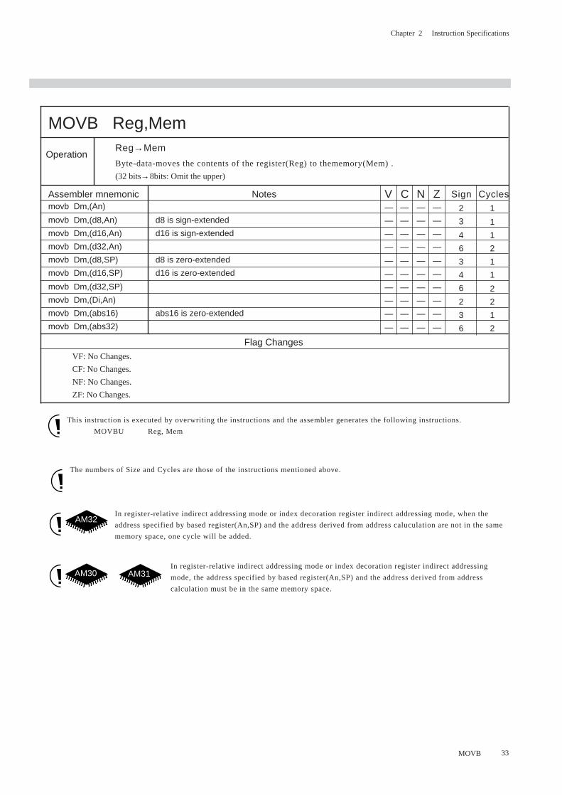
Chapter 2 Instruction Specifications
33
MOVB Reg,Mem
Operation
Assembler mnemonic
Reg→Mem
Byte-data-moves the contents of the register(Reg) to thememory(Mem) .
(32 bits→8bits: Omit the upper)
Sign Cyclesmovb Dm,(An)
movb Dm,(d8,An) d8 is sign-extended
movb Dm,(d16,An) d16 is sign-extended
movb Dm,(d32,An)
movb Dm,(d8,SP) d8 is zero-extended
movb Dm,(d16,SP) d16 is zero-extended
movb Dm,(d32,SP)
movb Dm,(Di,An)
movb Dm,(abs16) abs16 is zero-extended
movb Dm,(abs32)
Notes
Flag Changes
VF: No Changes.
CF: No Changes.
NF: No Changes.
ZF: No Changes.
2
3
4
6
3
4
6
2
3
6
1
1
1
2
1
1
2
2
1
2
This instruction is executed by overwriting the instructions and the assembler generates the following instructions.
MOVBU Reg, Mem
The numbers of Size and Cycles are those of the instructions mentioned above.
V C ZN—
—
—
—
—
—
—
—
—
—
—
—
—
—
—
—
—
—
—
—
—
—
—
—
—
—
—
—
—
—
—
—
—
—
—
—
—
—
—
—
In register-relative indirect addressing mode or index decoration register indirect addressing
mode, the address specified by based register(An,SP) and the address derived from address
calculation must be in the same memory space.
AM30 AM31
MOVB
In register-relative indirect addressing mode or index decoration register indirect addressing mode, when the
address specified by based register(An,SP) and the address derived from address caluculation are not in the same
memory space, one cycle will be added.
AM32M
OV
B
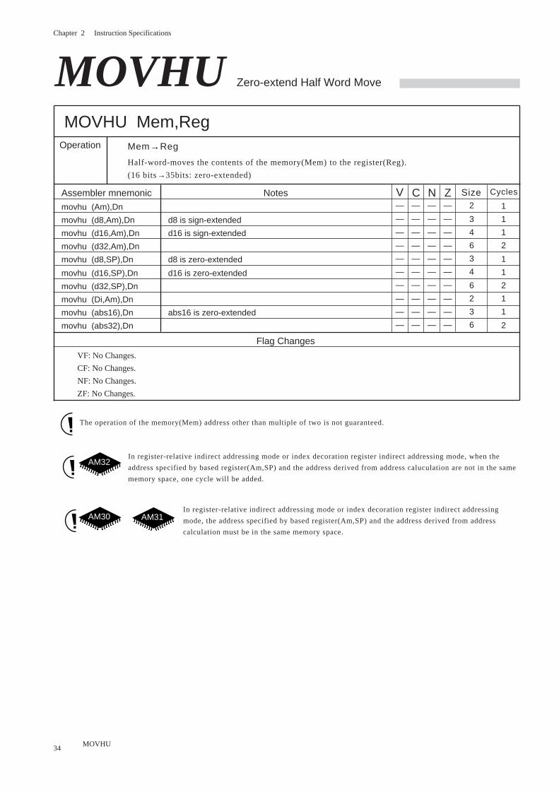
Chapter 2 Instruction Specifications
34
MOVHU Zero-extend Half Word Move
MOVHU Mem,RegOperation Mem→Reg
Half-word-moves the contents of the memory(Mem) to the register(Reg).
(16 bits→35bits: zero-extended)
The operation of the memory(Mem) address other than multiple of two is not guaranteed.
Assembler mnemonic Size Cycles
movhu (Am),Dn
movhu (d8,Am),Dn d8 is sign-extended
movhu (d16,Am),Dn d16 is sign-extended
movhu (d32,Am),Dn
movhu (d8,SP),Dn d8 is zero-extended
movhu (d16,SP),Dn d16 is zero-extended
movhu (d32,SP),Dn
movhu (Di,Am),Dn
movhu (abs16),Dn abs16 is zero-extended
movhu (abs32),Dn
Notes
Flag Changes
VF: No Changes.
CF: No Changes.
NF: No Changes.
ZF: No Changes.
1
1
1
2
1
1
2
1
1
2
2
3
4
6
3
4
6
2
3
6
MOVHU
V C ZN—
—
—
—
—
—
—
—
—
—
—
—
—
—
—
—
—
—
—
—
—
—
—
—
—
—
—
—
—
—
—
—
—
—
—
—
—
—
—
—
In register-relative indirect addressing mode or index decoration register indirect addressing
mode, the address specified by based register(Am,SP) and the address derived from address
calculation must be in the same memory space.
AM30 AM31
In register-relative indirect addressing mode or index decoration register indirect addressing mode, when the
address specified by based register(Am,SP) and the address derived from address caluculation are not in the same
memory space, one cycle will be added.
AM32
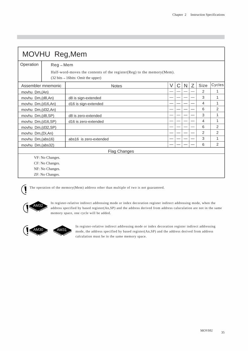
Chapter 2 Instruction Specifications
35
MOVHU Reg,MemOperation Reg→Mem
Half-word-moves the contents of the register(Reg) to the memory(Mem).
(32 bits→16bits: Omit the upper)
The operation of the memory(Mem) address other than multiple of two is not guaranteed.
Assembler mnemonic Size CyclesNotes
Flag Changes
VF: No Changes.
CF: No Changes.
NF: No Changes.
ZF: No Changes.
2
3
4
6
3
4
6
2
3
6
1
1
1
2
1
1
2
2
1
2
movhu Dm,(An)
movhu Dm,(d8,An) d8 is sign-extended
movhu Dm,(d16,An) d16 is sign-extended
movhu Dm,(d32,An)
movhu Dm,(d8,SP) d8 is zero-extended
movhu Dm,(d16,SP) d16 is zero-extended
movhu Dm,(d32,SP)
movhu Dm,(Di,An)
movhu Dm,(abs16) abs16 is zero-extended
movhu Dm,(abs32)
MOVHU
V C ZN—
—
—
—
—
—
—
—
—
—
—
—
—
—
—
—
—
—
—
—
—
—
—
—
—
—
—
—
—
—
—
—
—
—
—
—
—
—
—
—
In register-relative indirect addressing mode or index decoration register indirect addressing
mode, the address specified by based register(An,SP) and the address derived from address
calculation must be in the same memory space.
AM30 AM31
In register-relative indirect addressing mode or index decoration register indirect addressing mode, when the
address specified by based register(An,SP) and the address derived from address caluculation are not in the same
memory space, one cycle will be added.
AM32
MO
VH
U
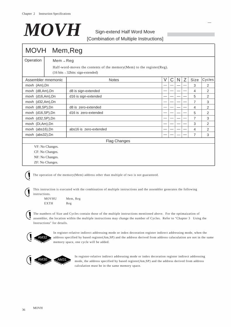
Chapter 2 Instruction Specifications
36
Sign-extend Half Word Move
[Combination of Multiple Instructions]
MOVH Mem,RegOperation Mem→Reg
Half-word-moves the contents of the memory(Mem) to the register(Reg).
(16 bits→32bits: sign-extended)
The operation of the memory(Mem) address other than multiple of two is not guaranteed.
MOVH
This instruction is executed with the combination of multiple instructions and the assembler generates the following
instructions.
MOVHU Mem, Reg
EXTH Reg
Assembler mnemonic Size Cycles
movh (Am),Dn
movh (d8,Am),Dn d8 is sign-extended
movh (d16,Am),Dn d16 is sign-extended
movh (d32,Am),Dn
movh (d8,SP),Dn d8 is zero-extended
movh (d16,SP),Dn d16 is zero-extended
movh (d32,SP),Dn
movh (Di,Am),Dn
movh (abs16),Dn abs16 is zero-extended
movh (abs32),Dn
Notes
Flag ChangesVF: No Changes.
CF: No Changes.
NF: No Changes.
ZF: No Changes.
3
4
5
7
4
5
7
3
4
7
2
2
2
3
2
2
3
2
2
3
MOVH
V C ZN—
—
—
—
—
—
—
—
—
—
—
—
—
—
—
—
—
—
—
—
—
—
—
—
—
—
—
—
—
—
—
—
—
—
—
—
—
—
—
—
In register-relative indirect addressing mode or index decoration register indirect addressing
mode, the address specified by based register(Am,SP) and the address derived from address
calculation must be in the same memory space.
In register-relative indirect addressing mode or index decoration register indirect addressing mode, when the
address specified by based register(Am,SP) and the address derived from address caluculation are not in the same
memory space, one cycle will be added.
The numbers of Size and Cycles contain those of the multiple instructions mentioned above. For the optimaization of
assembler, the location within the multiple instructions may change the number of Cycles. Refer to "Chapter 3 Using the
Instructions" for details.
AM30 AM31
AM32
—
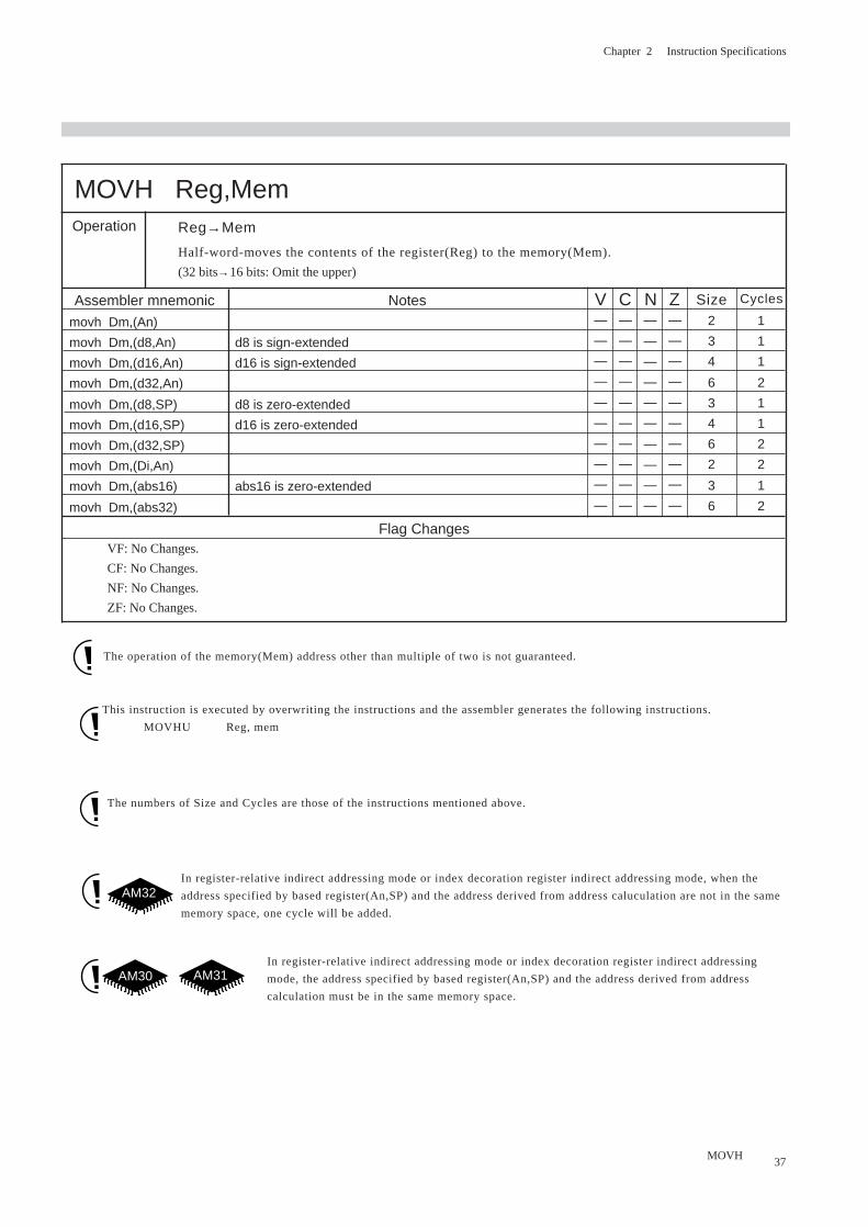
Chapter 2 Instruction Specifications
37
MOVH Reg,MemOperation Reg→Mem
Half-word-moves the contents of the register(Reg) to the memory(Mem).
(32 bits→16 bits: Omit the upper)
The operation of the memory(Mem) address other than multiple of two is not guaranteed. EX
T
Assembler mnemonic Size Cycles
movh Dm,(An)
movh Dm,(d8,An) d8 is sign-extended
movh Dm,(d16,An) d16 is sign-extended
movh Dm,(d32,An)
movh Dm,(d8,SP) d8 is zero-extended
movh Dm,(d16,SP) d16 is zero-extended
movh Dm,(d32,SP)
movh Dm,(Di,An)
movh Dm,(abs16) abs16 is zero-extended
movh Dm,(abs32)
Notes
Flag ChangesVF: No Changes.
CF: No Changes.
NF: No Changes.
ZF: No Changes.
2
3
4
6
3
4
6
2
3
6
1
1
1
2
1
1
2
2
1
2
MOVH
V C ZN—
—
—
—
—
—
—
—
—
—
—
—
—
—
—
—
—
—
—
—
—
—
—
—
—
—
—
—
—
—
—
—
—
—
—
—
—
—
—
—
In register-relative indirect addressing mode or index decoration register indirect addressing
mode, the address specified by based register(An,SP) and the address derived from address
calculation must be in the same memory space.
AM30
In register-relative indirect addressing mode or index decoration register indirect addressing mode, when the
address specified by based register(An,SP) and the address derived from address caluculation are not in the same
memory space, one cycle will be added.
This instruction is executed by overwriting the instructions and the assembler generates the following instructions.
MOVHU Reg, mem
The numbers of Size and Cycles are those of the instructions mentioned above.
AM31
AM32
MO
VH
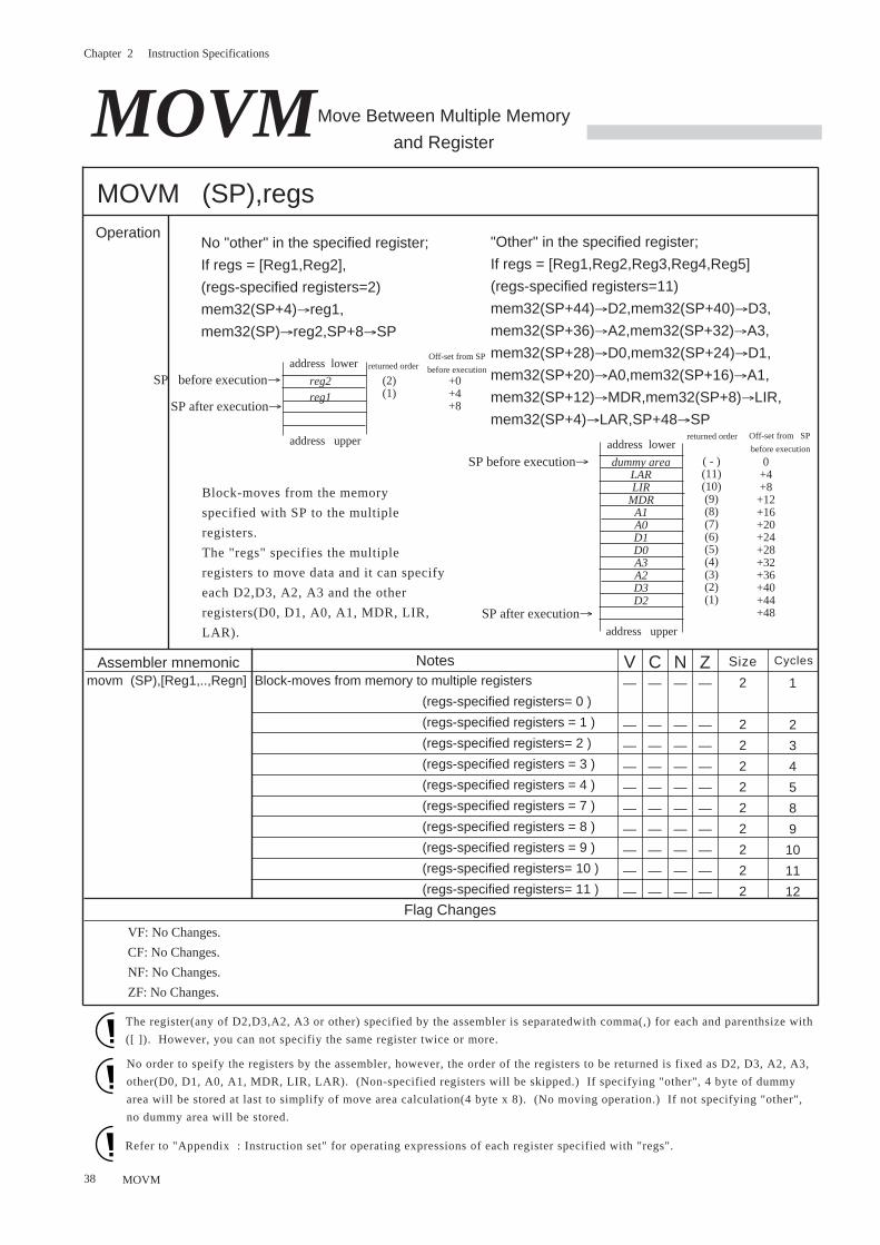
Chapter 2 Instruction Specifications
38
Size CyclesNotes
2
2
2
2
2
2
2
2
2
2
1
2
3
4
5
8
9
10
11
12
Assembler mnemonicmovm (SP),[Reg1,..,Regn] Block-moves from memory to multiple registers
(regs-specified registers= 0 )
(regs-specified registers = 1 )
(regs-specified registers= 2 )
(regs-specified registers = 3 )
(regs-specified registers = 4 )
(regs-specified registers = 7 )
(regs-specified registers = 8 )
(regs-specified registers = 9 )
(regs-specified registers= 10 )
(regs-specified registers= 11 )
Move Between Multiple Memory
and Register
MOVM (SP),regsOperation
No "other" in the specified register;
If regs = [Reg1,Reg2],
(regs-specified registers=2)
mem32(SP+4)→reg1,
mem32(SP)→reg2,SP+8→SP
Block-moves from the memory
specified with SP to the multiple
registers.
The "regs" specifies the multiple
registers to move data and it can specify
each D2,D3, A2, A3 and the other
registers(D0, D1, A0, A1, MDR, LIR,
LAR).
MOVM
MOVM
Flag Changes
VF: No Changes.
CF: No Changes.
NF: No Changes.
ZF: No Changes.
V C ZN—
—
—
—
—
—
—
—
—
—
—
—
—
—
—
—
—
—
—
—
—
—
—
—
—
—
—
—
—
—
—
—
—
—
—
—
—
—
—
—
"Other" in the specified register;
If regs = [Reg1,Reg2,Reg3,Reg4,Reg5]
(regs-specified registers=11)
mem32(SP+44)→D2,mem32(SP+40)→D3,
mem32(SP+36)→A2,mem32(SP+32)→A3,
mem32(SP+28)→D0,mem32(SP+24)→D1,
mem32(SP+20)→A0,mem32(SP+16)→A1,
mem32(SP+12)→MDR,mem32(SP+8)→LIR,
mem32(SP+4)→LAR,SP+48→SP
Off-set from SP
before executionSP before execution→ reg2
reg1
(2)(1)
+0+4+8
address lower
address upper
returned order
The register(any of D2,D3,A2, A3 or other) specified by the assembler is separatedwith comma(,) for each and parenthsize with
([ ]). However, you can not specifiy the same register twice or more.
No order to speify the registers by the assembler, however, the order of the registers to be returned is fixed as D2, D3, A2, A3,
other(D0, D1, A0, A1, MDR, LIR, LAR). (Non-specified registers will be skipped.) If specifying "other", 4 byte of dummy
area will be stored at last to simplify of move area calculation(4 byte x 8). (No moving operation.) If not specifying "other",
no dummy area will be stored.
Refer to "Appendix : Instruction set" for operating expressions of each register specified with "regs".
SP after execution→
SP before execution→
SP after execution→
( - )(11)(10)(9)(8)(7)(6)(5)(4)(3)(2)(1)
returned order
0+4+8
+12+16+20+24+28+32+36+40+44+48
Off-set from SP
before execution
dummy areaLARLIR
MDRA1A0D1D0A3A2D3D2
address lower
address upper
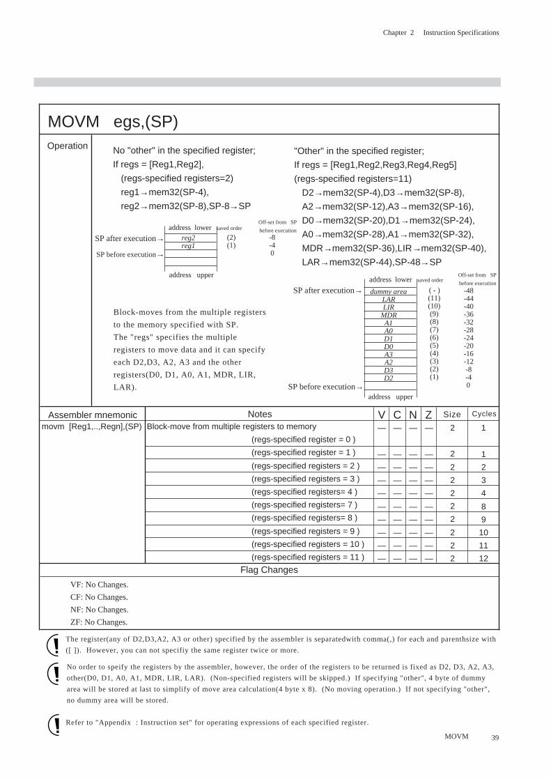
Chapter 2 Instruction Specifications
39
Size CyclesNotes
2
2
2
2
2
2
2
2
2
2
1
1
2
3
4
8
9
10
11
12
Assembler mnemonicmovm [Reg1,..,Regn],(SP) Block-move from multiple registers to memory
(regs-specified register = 0 )
(regs-specified register = 1 )
(regs-specified registers = 2 )
(regs-specified registers = 3 )
(regs-specified registers= 4 )
(regs-specified registers= 7 )
(regs-specified registers= 8 )
(regs-specified registers = 9 )
(regs-specified registers = 10 )
(regs-specified registers = 11 )
MOVM egs,(SP)Operation No "other" in the specified register;
If regs = [Reg1,Reg2],
(regs-specified registers=2)
reg1→mem32(SP-4),
reg2→mem32(SP-8),SP-8→SP
Block-moves from the multiple registers
to the memory specified with SP.
The "regs" specifies the multiple
registers to move data and it can specify
each D2,D3, A2, A3 and the other
registers(D0, D1, A0, A1, MDR, LIR,
LAR).
Flag Changes
VF: No Changes.
CF: No Changes.
NF: No Changes.
ZF: No Changes.
V C ZN—
—
—
—
—
—
—
—
—
—
—
—
—
—
—
—
—
—
—
—
—
—
—
—
—
—
—
—
—
—
—
—
—
—
—
—
—
—
—
—
"Other" in the specified register;
If regs = [Reg1,Reg2,Reg3,Reg4,Reg5]
(regs-specified registers=11)
D2→mem32(SP-4),D3→mem32(SP-8),
A2→mem32(SP-12),A3→mem32(SP-16),
D0→mem32(SP-20),D1→mem32(SP-24),
A0→mem32(SP-28),A1→mem32(SP-32),
MDR→mem32(SP-36),LIR→mem32(SP-40),
LAR→mem32(SP-44),SP-48→SP
SP after execution→ dummy areaLARLIR
MDRA1A0D1D0A3A2D3D2
( - )(11)(10)(9)(8)(7)(6)(5)(4)(3)(2)(1)
-48-44-40-36-32-28-24-20-16-12-8-40SP before execution→
address lower
address upper
saved orderOff-set from SP
before execution
Off-set from SP
before execution
SP after execution→ reg2reg1
(2)(1)
-8-40SP before execution→
address lower
address upper
saved order
The register(any of D2,D3,A2, A3 or other) specified by the assembler is separatedwith comma(,) for each and parenthsize with
([ ]). However, you can not specifiy the same register twice or more.
No order to speify the registers by the assembler, however, the order of the registers to be returned is fixed as D2, D3, A2, A3,
other(D0, D1, A0, A1, MDR, LIR, LAR). (Non-specified registers will be skipped.) If specifying "other", 4 byte of dummy
area will be stored at last to simplify of move area calculation(4 byte x 8). (No moving operation.) If not specifying "other",
no dummy area will be stored.
Refer to "Appendix : Instruction set" for operating expressions of each specified register.
MOVM
MO
VM
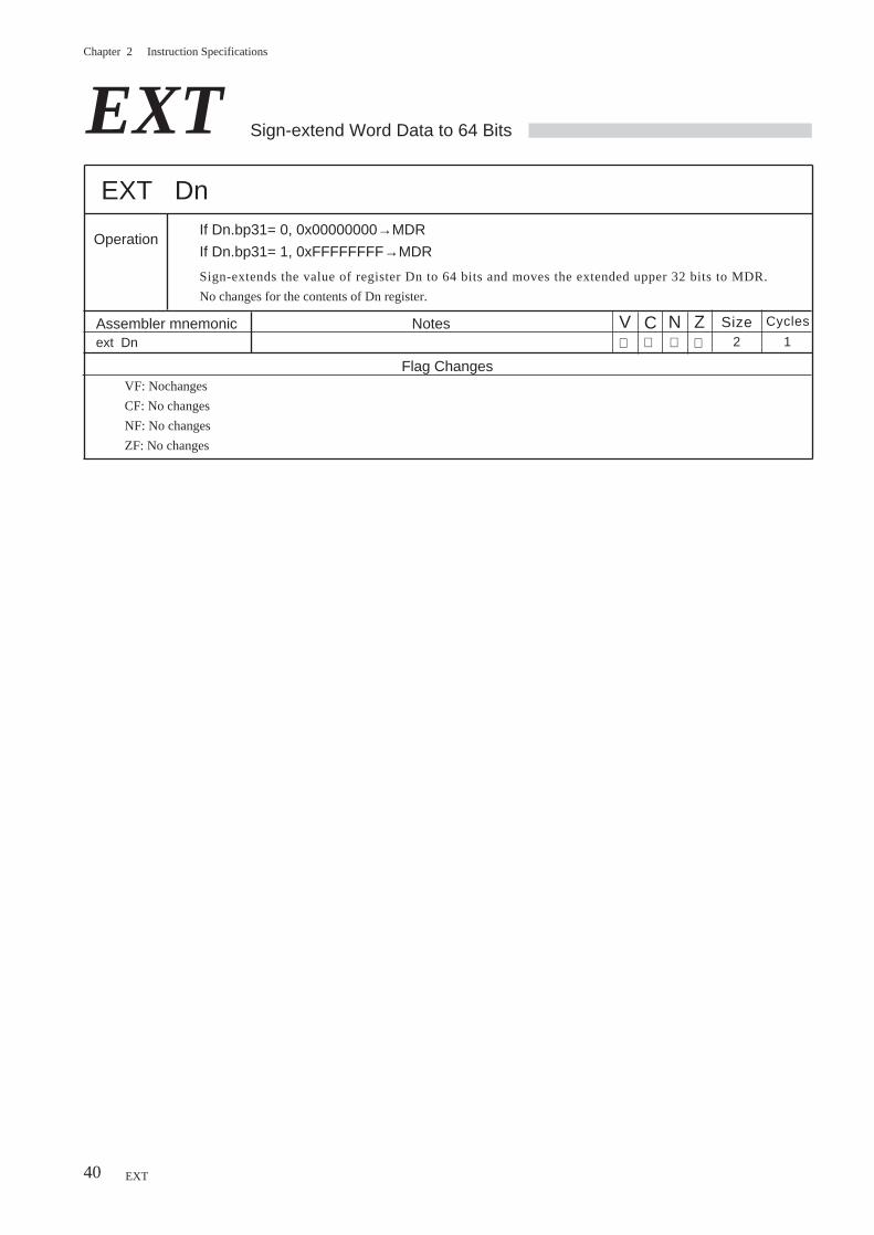
Chapter 2 Instruction Specifications
40
Sign-extend Word Data to 64 Bits
EXT Dn
V C Z
OperationIf Dn.bp31= 0, 0x00000000→MDR
If Dn.bp31= 1, 0xFFFFFFFF→MDR
Sign-extends the value of register Dn to 64 bits and moves the extended upper 32 bits to MDR.
No changes for the contents of Dn register.
SizeN2 1
EXT
CyclesNotes
Flag ChangesVF: Nochanges
CF: No changes
NF: No changes
ZF: No changes
Assembler mnemonicext Dn
EXT
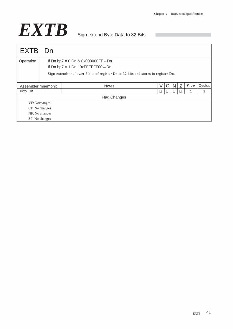
Chapter 2 Instruction Specifications
41
Sign-extend Byte Data to 32 Bits
EXTB DnOperation If Dn.bp7 = 0,Dn & 0x000000FF→Dn
If Dn.bp7 = 1,Dn | 0xFFFFFF00→Dn
Sign-extends the lower 8 bits of register Dn to 32 bits and stores in register Dn.
Size Cycles
1 1
EXTB
Assembler mnemonic Notes
Flag ChangesVF: Nochanges
CF: No changes
NF: No changes
ZF: No changes
extb Dn
EXTB
V C ZN
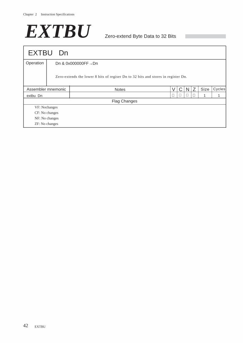
Chapter 2 Instruction Specifications
42
Zero-extend Byte Data to 32 Bits
EXTBU DnOperation Dn & 0x000000FF→Dn
Zero-extends the lower 8 bits of regiser Dn to 32 bits and stores in register Dn.
EXTBU
Size CyclesNotes
Flag Changes
VF: Nochanges
CF: No changes
NF: No changes
ZF: No changes
1 1
Assembler mnemonic
extbu Dn
EXTBU
V C ZN
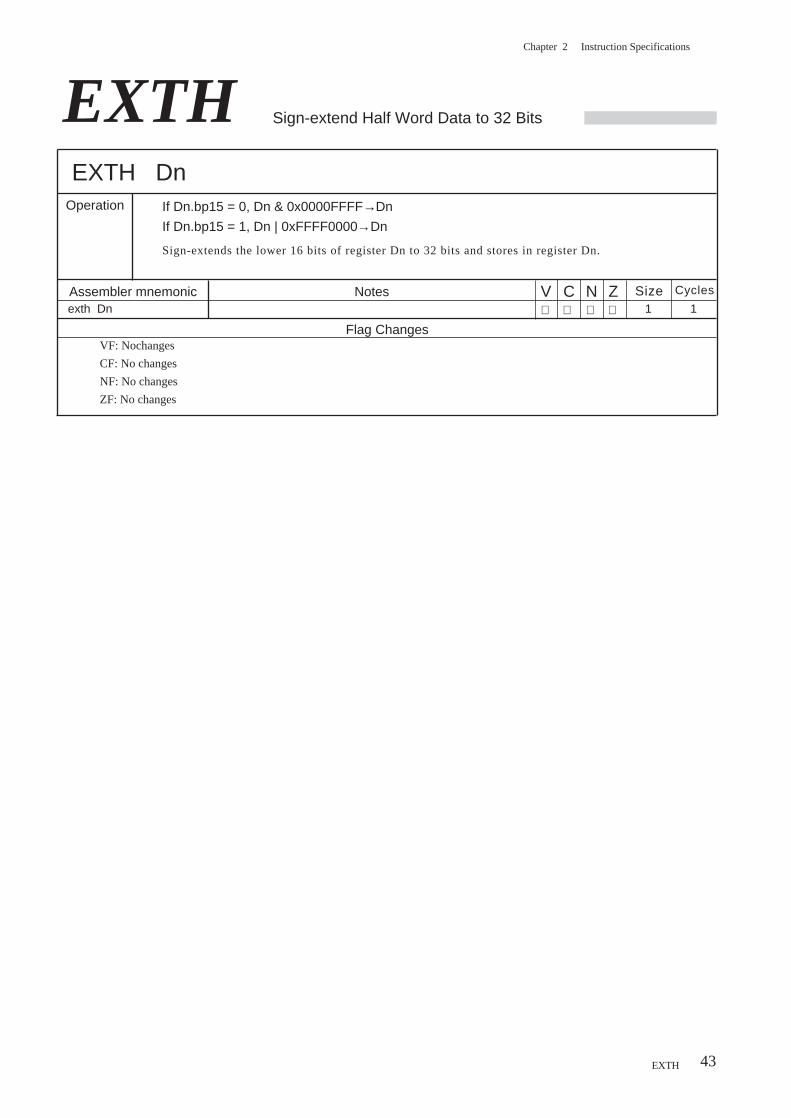
Chapter 2 Instruction Specifications
43
Sign-extend Half Word Data to 32 Bits
EXTH DnOperation If Dn.bp15 = 0, Dn & 0x0000FFFF→Dn
If Dn.bp15 = 1, Dn | 0xFFFF0000→Dn
Sign-extends the lower 16 bits of register Dn to 32 bits and stores in register Dn.
Size Cycles
VF: Nochanges
CF: No changes
NF: No changes
ZF: No changes
1 1
EXTH
Notes
Flag Changes
Assembler mnemonicexth Dn
EXTH
V C ZN
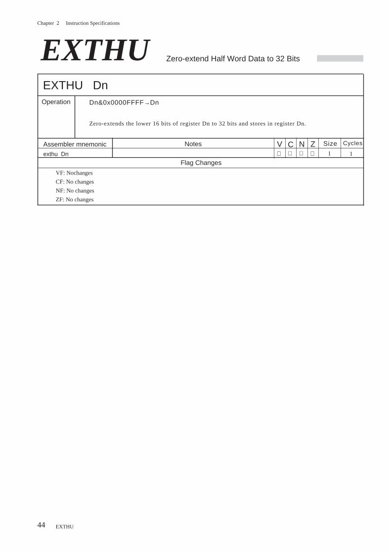
Chapter 2 Instruction Specifications
44
Zero-extend Half Word Data to 32 Bits
EXTHU DnOperation Dn&0x0000FFFF→Dn
Zero-extends the lower 16 bits of register Dn to 32 bits and stores in register Dn.
EXTHU
Size Cycles
Flag Changes
VF: Nochanges
CF: No changes
NF: No changes
ZF: No changes
1 1
Assembler mnemonic
exthu Dn
Notes
EXTHU
V C ZN
Chapter 2 Instruction Specifications
45
Data Clear
CLR DnOperation 0→Dn
Clears the contents of register Dn.
CLR
Size CyclesNotes
Flag Changes
VF: Always 0
CF: Always 0
NF: Always 0
ZF: Always 1
1 1
Assembler mnemonic
clr Dn
CLR
V C ZN● ● ● 1
One instruction is delayed when updating PSW by flag-change.
However, Bcc and Lcc instructions can evaluate the flag before affecting the flag.
Chapter 2 Instruction Specifications
46
ADD Addition
ADD Reg1,Reg2
V C Z●
●
●
●
Operation Reg1+Reg2→Reg2
Adds the contents of the register(Reg1) and the register(Reg2) and stores the results in the
register(Reg2).
NAssembler mnemonic Size Cycles
add Dm,Dn
add Dm,An
add Am,Dn
add Am,An
Notes
Updating of PSW due to flag changes is delayed for one insturuction.
However, Bcc and Lcc instructions can evaluate flag before reflecting to PSW.
1
2
2
2
1
1
1
1
Flag Changes
VF: 1 if an overflow is generated as 32 bits signed-numeric value; 0 otherwise.
CF: 1 if a carry is generated from bit 31; 0 otherwise.
NF: 1 if the bit 31 of the result is '1'; 0 otherwise.
ZF: 1 if the result is '0'; 0 othewise.
ADD
●
●
●
●
●
●
●
●
●
●
●
●
Chapter 2 Instruction Specifications
47
ADD imm,RegOperation imm+Reg→Reg
Adds the immediate value(imm) and the contents of the register(Reg) and stores the result in the
register(Reg).
Assembler mnemonic Size Cycles
add imm8,Dn imm8 is sign-extended.
add imm16,Dn imm16 is sign-extended.
add imm32,Dn
add imm8,An imm8 is sign-extended.
add imm16,An imm16 is sign-extended.
add imm32,An
add imm8,SP imm8 is sign-extended.
add imm16,SP imm16 is sign-extended.
add imm32,SP
Notes
Flag Change
Updating of PSW due to flag changes is delayed for one insturuction.
However, Bcc and Lcc instructions can evaluate flag before reflecting to PSW.
2
4
6
2
4
6
3
4
6
1
1
2
1
1
2
1
1
2
Other than add imm,SP
VF: 1 if an overflow is generated as 32 bits signed numeric value; 0 otherwise.
CF: 1 if a carry is generated from bit 31; 0 otherwise.
NF: 1 if the bit 31 of the result is '1'; 0 otherwise.
ZF: 1 if the result is '0'; 0 othewise.
add imm,SP
VF: No Changes.
CF: No Changes.
NF: No Changes.
ZF: No Changes.
ADD
V C Z●
●
●
●
●
●
N●
●
●
●
●
●
●
●
●
●
●
●
●
●
●
●
●
Add
ition
●
Chapter 2 Instruction Specifications
48
ADDC Addition With Carry
ADDC Dm,DnOperation Dm+Dn+CF→Dn
Adds the contents of register Dm including C flag and register Dn and stores the result in the register
Dn.
Size Cycles
addc Dm,Dn
Notes
Updating of PSW due to flag changes is delayed for one insturuction.
However, Bcc and Lcc instructions can evaluate flag before reflecting to PSW.
2 1
Flag ChangesVF: 1 if an overflow is generated as 32 bits signed-numeric value; 0 otherwise.
CF: 1 if a carry is generated from bit 31; 0 otherwise.
NF: 1 if the bit 31 of the result is '1'; 0 otherwise.
ZF: 1 if the result is '0'; 0 othewise.
Assembler mnemonic
ADDC
V C Z●
N● ● ●
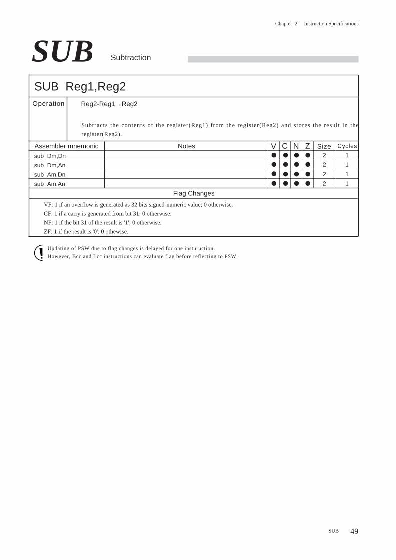
Chapter 2 Instruction Specifications
49
SUB Subtraction
SUB Reg1,Reg2Operation Reg2-Reg1→Reg2
Subtracts the contents of the register(Reg1) from the register(Reg2) and stores the result in the
register(Reg2).
Assembler mnemonic Size Cycles
sub Dm,Dn
sub Dm,An
sub Am,Dn
sub Am,An
Notes
Updating of PSW due to flag changes is delayed for one insturuction.
However, Bcc and Lcc instructions can evaluate flag before reflecting to PSW.
2
2
2
2
1
1
1
1
Flag Changes
VF: 1 if an overflow is generated as 32 bits signed-numeric value; 0 otherwise.
CF: 1 if a carry is generated from bit 31; 0 otherwise.
NF: 1 if the bit 31 of the result is '1'; 0 otherwise.
ZF: 1 if the result is '0'; 0 othewise.
SUB
V C Z●
●
●
●
N●
●
●
●
●
●
●
●
●
●
●
●
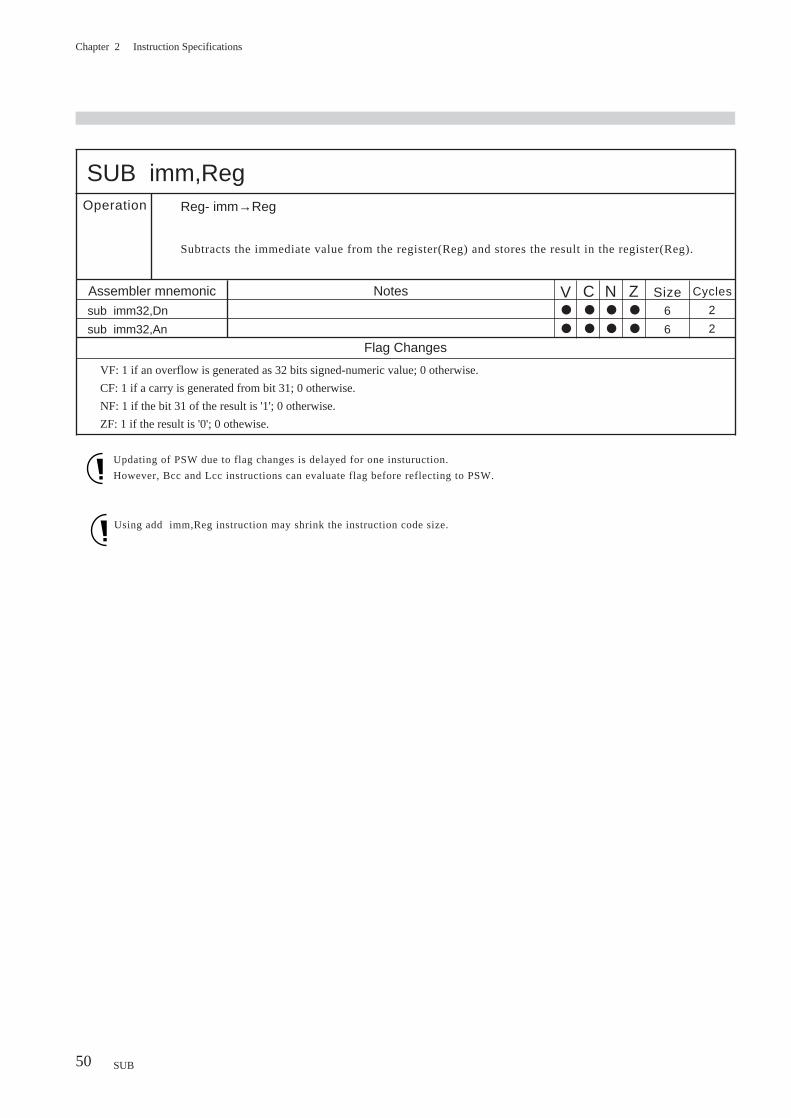
Chapter 2 Instruction Specifications
50
SUB imm,RegOperation Reg- imm→Reg
Assembler mnemonic
Subtracts the immediate value from the register(Reg) and stores the result in the register(Reg).
Size Cycles
sub imm32,Dn
sub imm32,An
Notes
Updating of PSW due to flag changes is delayed for one insturuction.
However, Bcc and Lcc instructions can evaluate flag before reflecting to PSW.
6
6
2
2
Flag Changes
VF: 1 if an overflow is generated as 32 bits signed-numeric value; 0 otherwise.
CF: 1 if a carry is generated from bit 31; 0 otherwise.
NF: 1 if the bit 31 of the result is '1'; 0 otherwise.
ZF: 1 if the result is '0'; 0 othewise.
SUB
Using add imm,Reg instruction may shrink the instruction code size.
V C Z●
●
N●
●
●
●
●
●
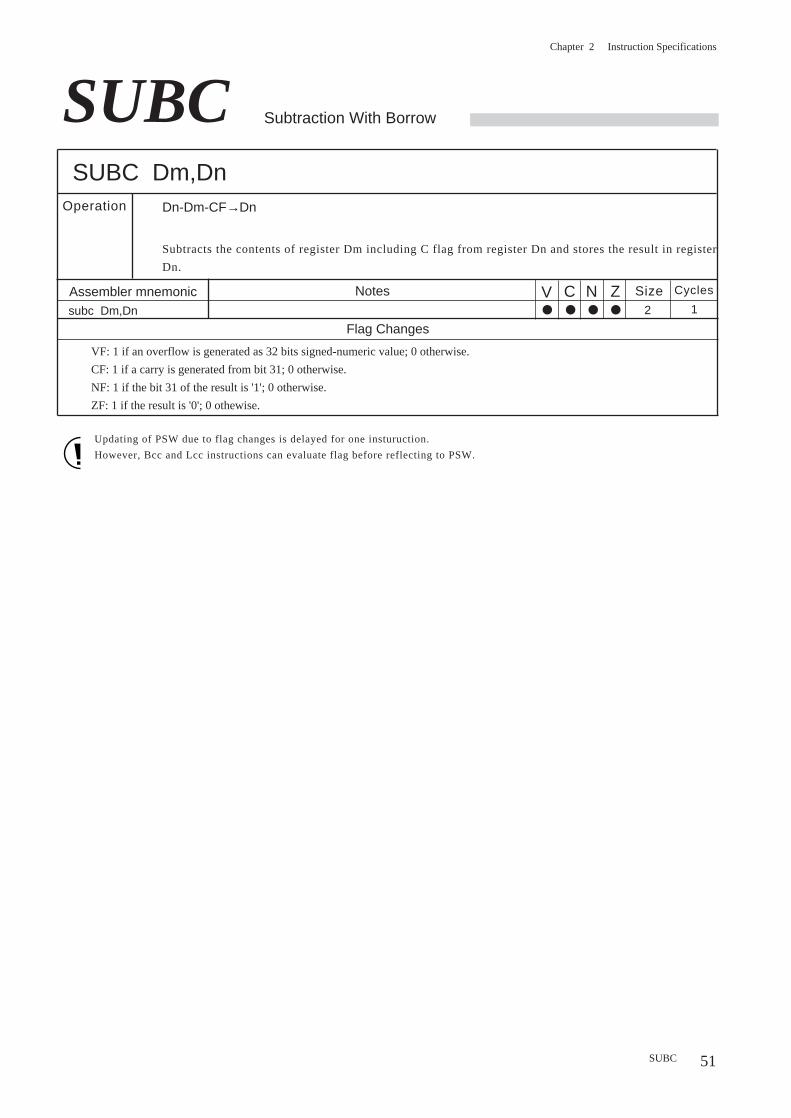
Chapter 2 Instruction Specifications
51
SUBC Subtraction With Borrow
SUBC Dm,DnOperation Dn-Dm-CF→Dn
Assembler mnemonic
Subtracts the contents of register Dm including C flag from register Dn and stores the result in register
Dn.
Size Cycles
subc Dm,Dn
Notes
Updating of PSW due to flag changes is delayed for one insturuction.
However, Bcc and Lcc instructions can evaluate flag before reflecting to PSW.
2 1
Flag Changes
VF: 1 if an overflow is generated as 32 bits signed-numeric value; 0 otherwise.
CF: 1 if a carry is generated from bit 31; 0 otherwise.
NF: 1 if the bit 31 of the result is '1'; 0 otherwise.
ZF: 1 if the result is '0'; 0 othewise.
SUBC
V C Z●
N● ● ●
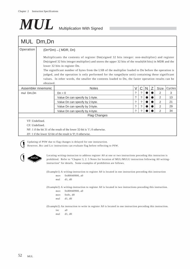
Chapter 2 Instruction Specifications
52
MUL Multiplication With Signed
MUL Dm,DnOperation (Dn*Dm)→{ MDR, Dn}
Multipl icants the contents of register Dm(signed 32 bits integer: non-multipl ier) and register
Dn(signed 32 bits integer:multiplier) and stores the upper 32 bits of the result(64 bits) in MDR and the
lower 32 bits in register Dn.
The siginificant number of bytes from the LSB of the multiplier loaded to Dn before the operation is
judged, and the operation is only performed for the range(byte unit) containing these significant
values. In other words, the smaller the contents loaded to Dn, the faster operation results can be
obtained.
mul Dm,Dn Dn = 0
Value Dn can specify by 1-byte.
Value Dn can specify by 2-byte.
Value Dn can specify by 3-byte.
Value Dn can specify by 4-byte.
Assembler mnemonic Size CyclesNotes2
2
2
2
2
3
13
21
29
34
Updating of PSW due to flag changes is delayed for one insturuction.
However, Bcc and Lcc instructions can evaluate flag before reflecting to PSW.
Flag Changes
VF: Undefined.
CF: Undefined.
NF: 1 if the bit 31 of the result of the lower 32-bit is '1'; 0 otherwise.
ZF: 1 if the lower 32-bit of the result is '0'; 0 otherwise.
Locating writing-instrucion to address register A0 at one or two instructions preceding this instrucion is
prohibited. Refer to "Chapter 3, 2. 5 Notes for location of MUL/MULU instruction following A0 writing-
instruction" for details. Some examples of prohibition are follows.
(Example1) A writing-instruction to register A0 is located in one instruction preceding this instruction
mov 0x80040900, a0
mul d1, d0
(Example2) A writing-instruction to register A0 is located in two instructions preceding this instruction.
mov 0x80040900, a0
mov 0x0c, d0
mul d1, d0
(Example2) An instruction to write in register A0 is located in one instruction preceding this instruction.
inc a0
mul d1, d0
MUL
V C Z?
?
?
?
?
N?
?
?
?
?
●
●
●
●
●
●
●
●
●
●
AM30
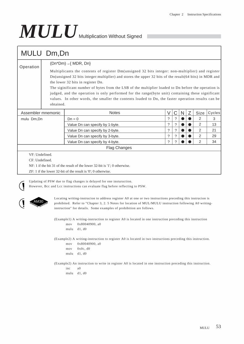
Chapter 2 Instruction Specifications
53
MULU Multiplication Without Signed
MULU Dm,Dn
Operation(Dn*Dm)→{ MDR, Dn}
Multiplicants the contents of register Dm(unsigned 32 bits integer: non-multiplier) and register
Dn(unsigned 32 bits integer:multiplier) and stores the upper 32 bits of the result(64 bits) in MDR and
the lower 32 bits in register Dn.
The siginificant number of bytes from the LSB of the multiplier loaded to Dn before the operation is
judged, and the operation is only performed for the range(byte unit) containing these significant
values. In other words, the smaller the contents loaded to Dn, the faster operation results can be
obtained.
mulu Dm,Dn Dn = 0
Value Dn can specify by 1-byte.
Value Dn can specify by 2-byte.
Value Dn can specify by 3-byte.
Value Dn can specify by 4-byte.
Assembler mnemonic Size CyclesNotes2
2
2
2
2
3
13
21
29
34
Updating of PSW due to flag changes is delayed for one insturuction.
However, Bcc and Lcc instructions can evaluate flag before reflecting to PSW.
Flag Changes
VF: Undefined.
CF: Undefined.
NF: 1 if the bit 31 of the result of the lower 32-bit is '1'; 0 otherwise.
ZF: 1 if the lower 32-bit of the result is '0'; 0 otherwise.
MULU
V C Z?
?
?
?
?
N?
?
?
?
?
●
●
●
●
●
●
●
●
●
●
Locating writing-instrucion to address register A0 at one or two instructions preceding this instrucion is
prohibited. Refer to "Chapter 3, 2. 5 Notes for location of MUL/MULU instruction following A0 writing-
instruction" for details. Some examples of prohibition are follows.
(Example1) A writing-instruction to register A0 is located in one instruction preceding this instruction
mov 0x80040900, a0
mulu d1, d0
(Example2) A writing-instruction to register A0 is located in two instructions preceding this instruction.
mov 0x80040900, a0
mov 0x0c, d0
mulu d1, d0
(Example2) An instruction to write in register A0 is located in one instruction preceding this instruction.
inc a0
mulu d1, d0
AM30
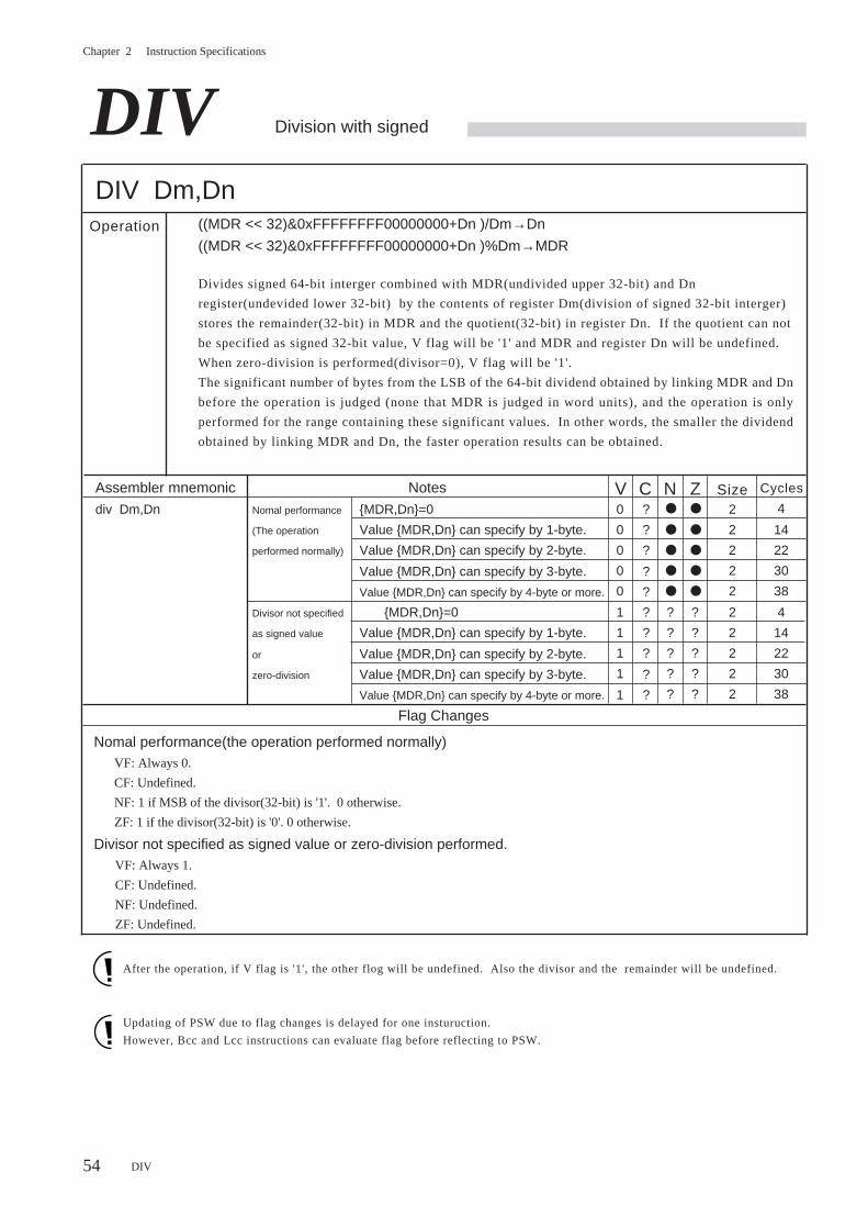
Chapter 2 Instruction Specifications
54
DIV Division with signed
DIV Dm,DnOperation ((MDR << 32)&0xFFFFFFFF00000000+Dn )/Dm→Dn
((MDR << 32)&0xFFFFFFFF00000000+Dn )%Dm→MDR
Divides signed 64-bit interger combined with MDR(undivided upper 32-bit) and Dn
register(undevided lower 32-bit) by the contents of register Dm(division of signed 32-bit interger)
stores the remainder(32-bit) in MDR and the quotient(32-bit) in register Dn. If the quotient can not
be specified as signed 32-bit value, V flag will be '1' and MDR and register Dn will be undefined.
When zero-division is performed(divisor=0), V flag will be '1'.
The significant number of bytes from the LSB of the 64-bit dividend obtained by linking MDR and Dn
before the operation is judged (none that MDR is judged in word units), and the operation is only
performed for the range containing these significant values. In other words, the smaller the dividend
obtained by linking MDR and Dn, the faster operation results can be obtained.
After the operation, if V flag is '1', the other flog will be undefined. Also the divisor and the remainder will be undefined.
Flag Changes
Nomal performance(the operation performed normally)VF: Always 0.
CF: Undefined.
NF: 1 if MSB of the divisor(32-bit) is '1'. 0 otherwise.
ZF: 1 if the divisor(32-bit) is '0'. 0 otherwise.
Divisor not specified as signed value or zero-division performed.VF: Always 1.
CF: Undefined.
NF: Undefined.
ZF: Undefined.
Updating of PSW due to flag changes is delayed for one insturuction.
However, Bcc and Lcc instructions can evaluate flag before reflecting to PSW.
div Dm,Dn Nomal performance {MDR,Dn}=0
(The operation Value {MDR,Dn} can specify by 1-byte.
performed normally) Value {MDR,Dn} can specify by 2-byte.
Value {MDR,Dn} can specify by 3-byte.
Value {MDR,Dn} can specify by 4-byte or more.
Divisor not specified {MDR,Dn}=0
as signed value Value {MDR,Dn} can specify by 1-byte.
or Value {MDR,Dn} can specify by 2-byte.
zero-division Value {MDR,Dn} can specify by 3-byte.
Value {MDR,Dn} can specify by 4-byte or more.
Assembler mnemonic Size CyclesNotes
2
2
2
2
2
2
2
2
2
2
4
14
22
30
38
4
14
22
30
38
DIV
V C Z0
0
0
0
0
1
1
1
1
1
N?
?
?
?
?
?
?
?
?
?
●
●
●
●
●
?
?
?
?
?
●
●
●
●
●
?
?
?
?
?
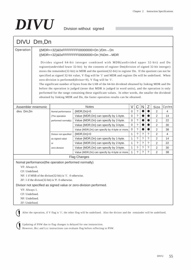
Chapter 2 Instruction Specifications
55
DIVU Division without signed
DIVU Dm,DnOperation
D iv ides s igned 64-b i t i n te rger combined w i th MDR(und iv ided upper 32-b i t ) and Dn
register(undevided lower 32-bit) by the contents of register Dm(division of signed 32-bit interger)
stores the remainder(32-bit) in MDR and the quotient(32-bit) in register Dn. If the quotient can not be
specified as signed 32-bit value, V flag will be '1' and MDR and register Dn will be undefined. When
zero-division is performed(divisor=0), V flag will be '1'.
The significant number of bytes from the LSB of the 64-bit dividend obtained by linking MDR and Dn
before the operation is judged (none that MDR is judged in word units), and the operation is only
performed for the range containing these significant values. In other words, the smaller the dividend
obtained by linking MDR and Dn, the faster operation results can be obtained.
((MDR<<32)&0xFFFFFFFF00000000+Dn )/Dm→Dn
((MDR<<32)&0xFFFFFFFF00000000+Dn )%Dm→MDR
Assembler mnemonic Size CyclesNotes2
2
2
2
2
2
2
2
2
2
4
14
22
30
38
4
14
22
30
38
After the operation, if V flag is '1', the other flog will be undefined. Also the divisor and the remainder will be undefined.
Flag Changes
Nomal performance(the operation performed normally)VF: Always 0.
CF: Undefined.
NF: 1 if MSB of the divisor(32-bit) is '1'. 0 otherwise.
ZF: 1 if the divisor(32-bit) is '0'. 0 otherwise.
Divisor not specified as signed value or zero-division performed.VF: Always 1.
CF: Undefined.
NF: Undefined.
ZF: Undefined.
Updating of PSW due to flag changes is delayed for one insturuction.
However, Bcc and Lcc instructions can evaluate flag before reflecting to PSW.
DIVU
V C Z0
0
0
0
0
1
1
1
1
1
N?
?
?
?
?
?
?
?
?
?
●
●
●
●
●
?
?
?
?
?
●
●
●
●
●
?
?
?
?
?
divu Dm,Dn Nomal performance {MDR,Dn}=0
(The operation Value {MDR,Dn} can specify by 1-byte.
performed normally) Value {MDR,Dn} can specify by 2-byte.
Value {MDR,Dn} can specify by 3-byte.
Value {MDR,Dn} can specify by 4-byte or more.
Divisor not specified {MDR,Dn}=0
as signed value Value {MDR,Dn} can specify by 1-byte.
or Value {MDR,Dn} can specify by 2-byte.
zero-division Value {MDR,Dn} can specify by 3-byte.
Value {MDR,Dn} can specify by 4-byte or more.
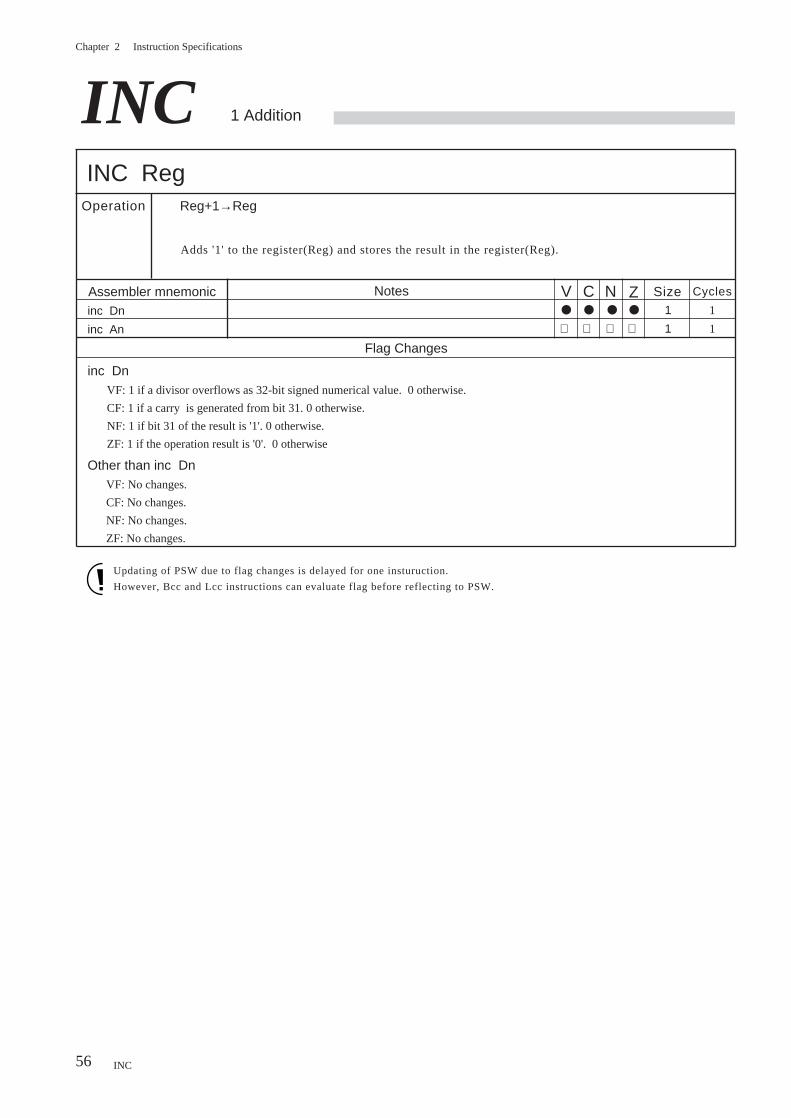
Chapter 2 Instruction Specifications
56
INC 1 Addition
INC RegOperation Reg+1→Reg
Adds '1' to the register(Reg) and stores the result in the register(Reg).
Assembler mnemonic Size Cycles
inc Dn
inc An
Notes
Updating of PSW due to flag changes is delayed for one insturuction.
However, Bcc and Lcc instructions can evaluate flag before reflecting to PSW.
1
1
1
1
Flag Changes
inc DnVF: 1 if a divisor overflows as 32-bit signed numerical value. 0 otherwise.
CF: 1 if a carry is generated from bit 31. 0 otherwise.
NF: 1 if bit 31 of the result is '1'. 0 otherwise.
ZF: 1 if the operation result is '0'. 0 otherwise
Other than inc DnVF: No changes.
CF: No changes.
NF: No changes.
ZF: No changes.
INC
V C Z●
N●
●
●
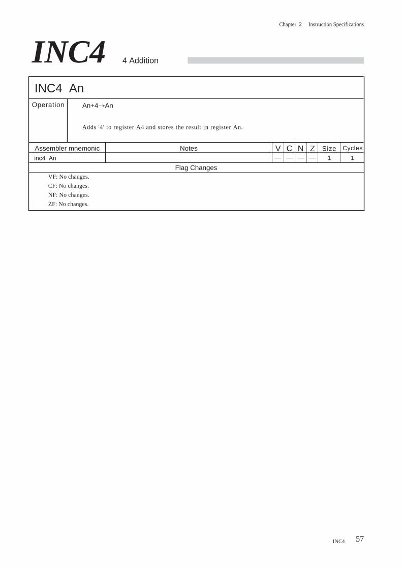
Chapter 2 Instruction Specifications
57
INC4 4 Addition
INC4 AnOperation An+4→An
Adds '4' to register A4 and stores the result in register An.
Assembler mnemonic Size Cycles
inc4 An
Notes1 1
Flag ChangesVF: No changes.
CF: No changes.
NF: No changes.
ZF: No changes.
INC4
V C Z
N
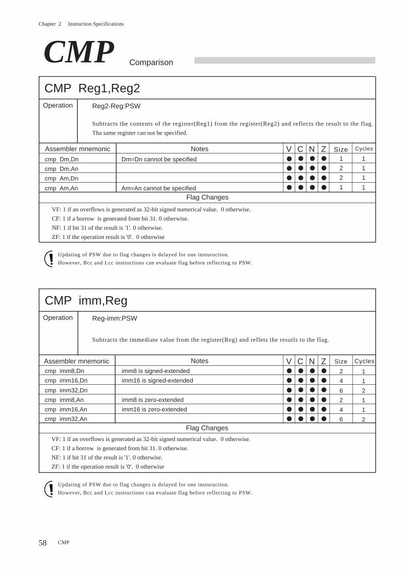
Chapter 2 Instruction Specifications
58
CMP Comparison
CMP Reg1,Reg2
V C Z
Operation Reg2-Reg:PSW
Subtracts the contents of the register(Reg1) from the register(Reg2) and reflects the result to the flag.
Tha same register can not be specified.
N
CMP imm,RegOperation Reg-imm:PSW
Subtracts the immediate value from the register(Reg) and reflets the resutls to the flag.
Assembler mnemonic Size Cycles
cmp Dm,Dn Dm=Dn cannot be specified
cmp Dm,An
cmp Am,Dn
cmp Am,An Am=An cannot be specified
Notes
Updating of PSW due to flag changes is delayed for one insturuction.
However, Bcc and Lcc instructions can evaluate flag before reflecting to PSW.
1
2
2
1
1
1
1
1
Flag Changes
VF: 1 if an overflows is generated as 32-bit signed numerical value. 0 otherwise.
CF: 1 if a borrow is generated from bit 31. 0 otherwise.
NF: 1 if bit 31 of the result is '1'. 0 otherwise.
ZF: 1 if the operation result is '0'. 0 otherwise
Assembler mnemonic Size Cycles
cmp imm8,Dn imm8 is signed-extended
cmp imm16,Dn imm16 is signed-extended
cmp imm32,Dn
cmp imm8,An imm8 is zero-extended
cmp imm16,An imm16 is zero-extended
cmp imm32,An
Notes
2
4
6
2
4
6
1
1
2
1
1
2Flag Changes
VF: 1 if an overflows is generated as 32-bit signed numerical value. 0 otherwise.
CF: 1 if a borrow is generated from bit 31. 0 otherwise.
NF: 1 if bit 31 of the result is '1'. 0 otherwise.
ZF: 1 if the operation result is '0'. 0 otherwise
Updating of PSW due to flag changes is delayed for one insturuction.
However, Bcc and Lcc instructions can evaluate flag before reflecting to PSW.
CMP
●
●
●
●
●
●
●
●
●
●
●
●
●
●
●
●
V C ZN●
●
●
●
●
●
●
●
●
●
●
●
●
●
●
●
●
●
●
●
●
●
●
●
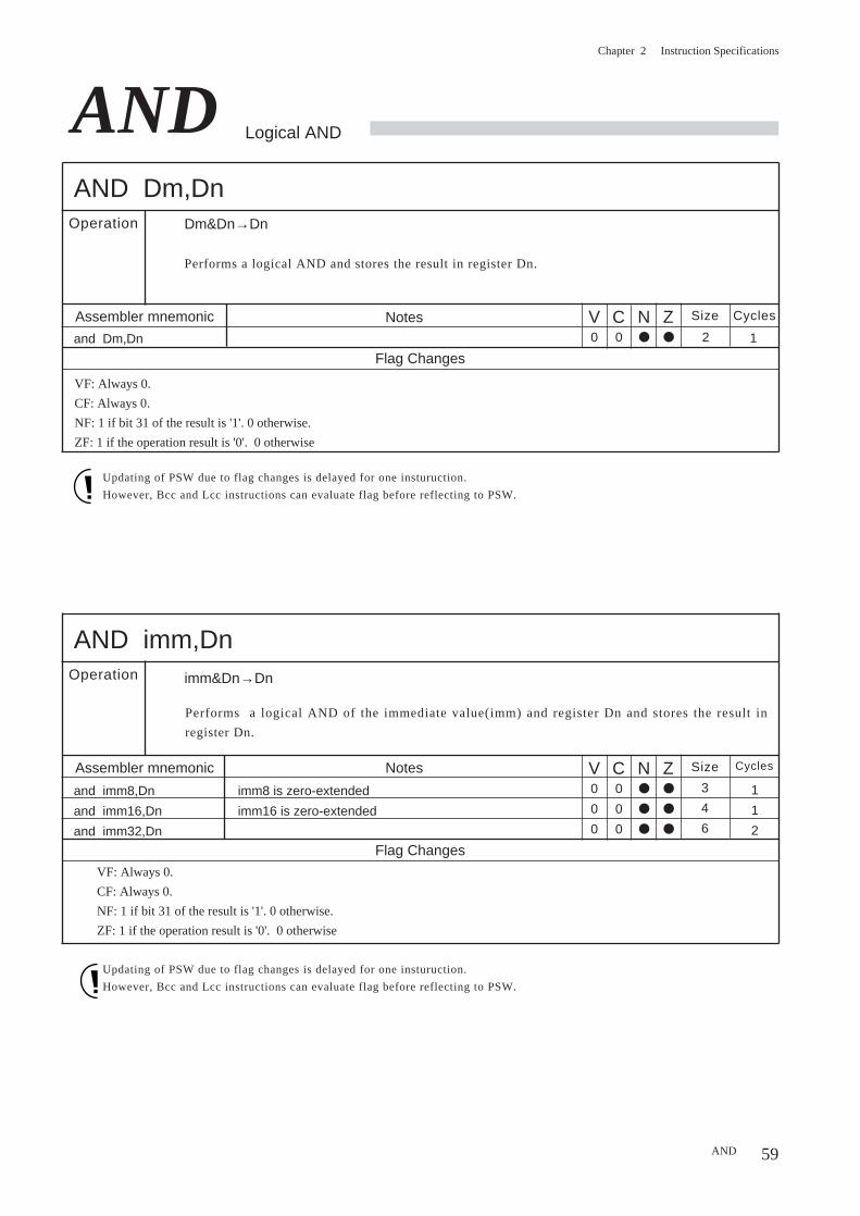
Chapter 2 Instruction Specifications
59
Performs a logical AND and stores the result in register Dn.
Performs a logical AND of the immediate value(imm) and register Dn and stores the result in
register Dn.
AND Logical AND
AND Dm,Dn
V C Z
Operation Dm&Dn→Dn
N
AND imm,DnOperation imm&Dn→Dn
Updating of PSW due to flag changes is delayed for one insturuction.
However, Bcc and Lcc instructions can evaluate flag before reflecting to PSW.
Size Cycles
and imm8,Dn imm8 is zero-extended
and imm16,Dn imm16 is zero-extended
and imm32,Dn
Notes3
4
6
1
1
2
Flag Changes
VF: Always 0.
CF: Always 0.
NF: 1 if bit 31 of the result is '1'. 0 otherwise.
ZF: 1 if the operation result is '0'. 0 otherwise
Assembler mnemonic
Size Cycles
and Dm,Dn
Notes2 1
Flag Changes
VF: Always 0.
CF: Always 0.
NF: 1 if bit 31 of the result is '1'. 0 otherwise.
ZF: 1 if the operation result is '0'. 0 otherwise
Assembler mnemonic
Updating of PSW due to flag changes is delayed for one insturuction.
However, Bcc and Lcc instructions can evaluate flag before reflecting to PSW.
AND
0 0 ● ●
V C ZN0
0
0
0
0
0
●
●
●
●
●
●
Com
paris
on
Inst
ruct
ion
Logi
cal O
pera
tion
Inst
ruct
ion
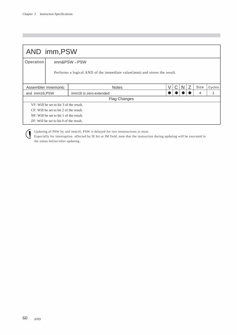
Chapter 2 Instruction Specifications
60
AND imm,PSWOperation imm&PSW→PSW
Performs a logical AND of the immediate value(imm) and stores the result.
Assembler mnemonic Size Cycles
and imm16,PSW imm16 is zero-extended
Notes4 1
Updating of PSW by and imm16, PSW is delayed for two instuructions at most.
Especially for interruption affected by IE bit or IM field, note that the instruction during updating will be executed in
the status before/after updating.
Flag Changes
VF: Will be set to bit 3 of the result.
CF: Will be set to bit 2 of the result.
NF: Will be set to bit 1 of the result.
ZF: Will be set to bit 0 of the result.
AND
V C ZN● ● ● ●
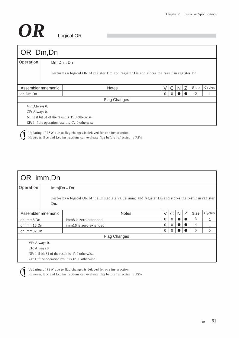
Chapter 2 Instruction Specifications
61
OR
Performs a logical OR of register Dm and register Dn and stores the result in register Dn.
Performs a logical OR of the immediate value(imm) and register Dn and stores the result in register
Dn.
Logical OR
OR Dm,DnOperation Dm|Dn→Dn
OR imm,DnOperation imm|Dn→Dn
Size Cycles
or Dm,Dn
Notes2 1
Flag Changes
VF: Always 0.
CF: Always 0.
NF: 1 if bit 31 of the result is '1'. 0 otherwise.
ZF: 1 if the operation result is '0'. 0 otherwise
Assembler mnemonic
Updating of PSW due to flag changes is delayed for one insturuction.
However, Bcc and Lcc instructions can evaluate flag before reflecting to PSW.
Updating of PSW due to flag changes is delayed for one insturuction.
However, Bcc and Lcc instructions can evaluate flag before reflecting to PSW.
Size Cycles
or imm8,Dn imm8 is zero-extended
or imm16,Dn imm16 is zero-extended
or imm32,Dn
Notes3
4
6
1
1
2
Flag Changes
VF: Always 0.
CF: Always 0.
NF: 1 if bit 31 of the result is '1'. 0 otherwise.
ZF: 1 if the operation result is '0'. 0 otherwise
Assembler mnemonic
OR
V C ZN0 0 ● ●
V C ZN0
0
0
0
0
0
●
●
●
●
●
●
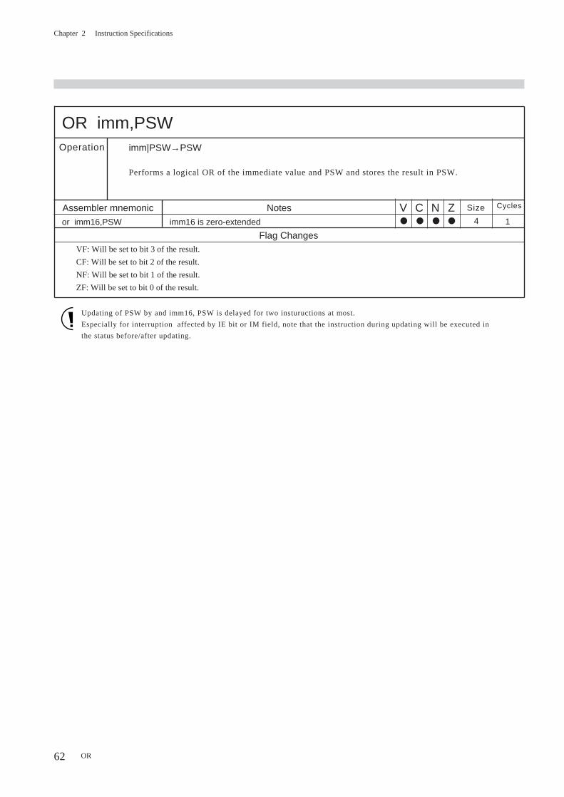
Chapter 2 Instruction Specifications
62
Performs a logical OR of the immediate value and PSW and stores the result in PSW.
OR imm,PSWOperation imm|PSW→PSW
Assembler mnemonic Size Cycles
or imm16,PSW imm16 is zero-extended
Notes4 1
Updating of PSW by and imm16, PSW is delayed for two instuructions at most.
Especially for interruption affected by IE bit or IM field, note that the instruction during updating will be executed in
the status before/after updating.
Flag ChangesVF: Will be set to bit 3 of the result.
CF: Will be set to bit 2 of the result.
NF: Will be set to bit 1 of the result.
ZF: Will be set to bit 0 of the result.
OR
V C ZN● ● ● ●

Chapter 2 Instruction Specifications
63
Performs an exclusive logical OR of register Dm and register Dn and stores the result in register
Dn.
XOR Exclusive Logical OR
XOR Dm,DnOperation Dm^Dn→Dn
XOR imm,DnOperation imm^Dn→Dn
Performs an exclusive logical OR of the immediate value and register Dn and stores the result in
register Dn.
Size Cycles
xor Dm,Dn
Notes2 1
Flag Changes
VF: Always 0.
CF: Always 0.
NF: 1 if bit 31 of the result is '1'. 0 otherwise.
ZF: 1 if the operation result is '0'. 0 otherwise
Assembler mnemonic
Updating of PSW due to flag changes is delayed for one insturuction.
However, Bcc and Lcc instructions can evaluate flag before reflecting to PSW.
Updating of PSW due to flag changes is delayed for one insturuction.
However, Bcc and Lcc instructions can evaluate flag before reflecting to PSW.
Size Cycles
xor imm16,Dn imm16 is zero-extended
xor imm32,Dn
Notes4
6
1
2
Flag Changes
VF: Always 0.
CF: Always 0.
NF: 1 if bit 31 of the result is '1'. 0 otherwise.
ZF: 1 if the operation result is '0'. 0 otherwise
Assembler mnemonic
XOR
V C ZN0 0 ● ●
V C ZN0
0
0
0
●
●
●
●
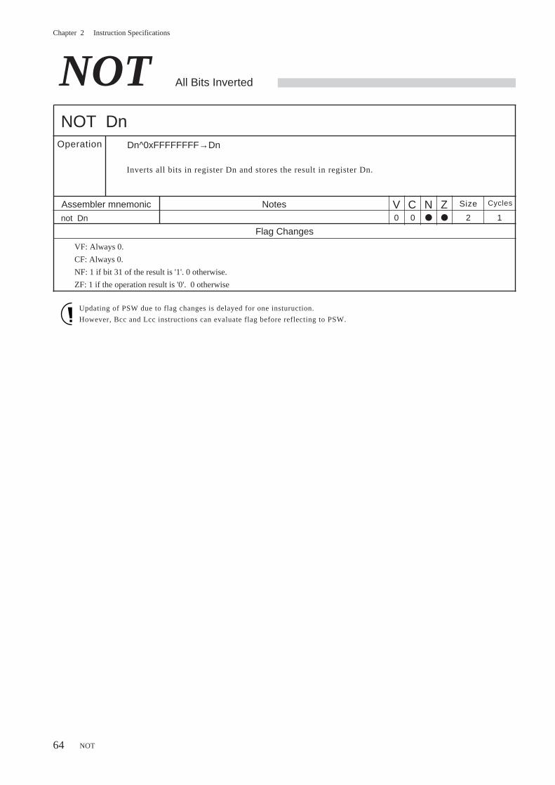
Chapter 2 Instruction Specifications
64
Inverts all bits in register Dn and stores the result in register Dn.
NOT All Bits Inverted
NOT DnOperation Dn^0xFFFFFFFF→Dn
Size Cycles
not Dn
Notes2 1
Flag Changes
VF: Always 0.
CF: Always 0.
NF: 1 if bit 31 of the result is '1'. 0 otherwise.
ZF: 1 if the operation result is '0'. 0 otherwise
Assembler mnemonic
Updating of PSW due to flag changes is delayed for one insturuction.
However, Bcc and Lcc instructions can evaluate flag before reflecting to PSW.
NOT
V C ZN0 ● ●0
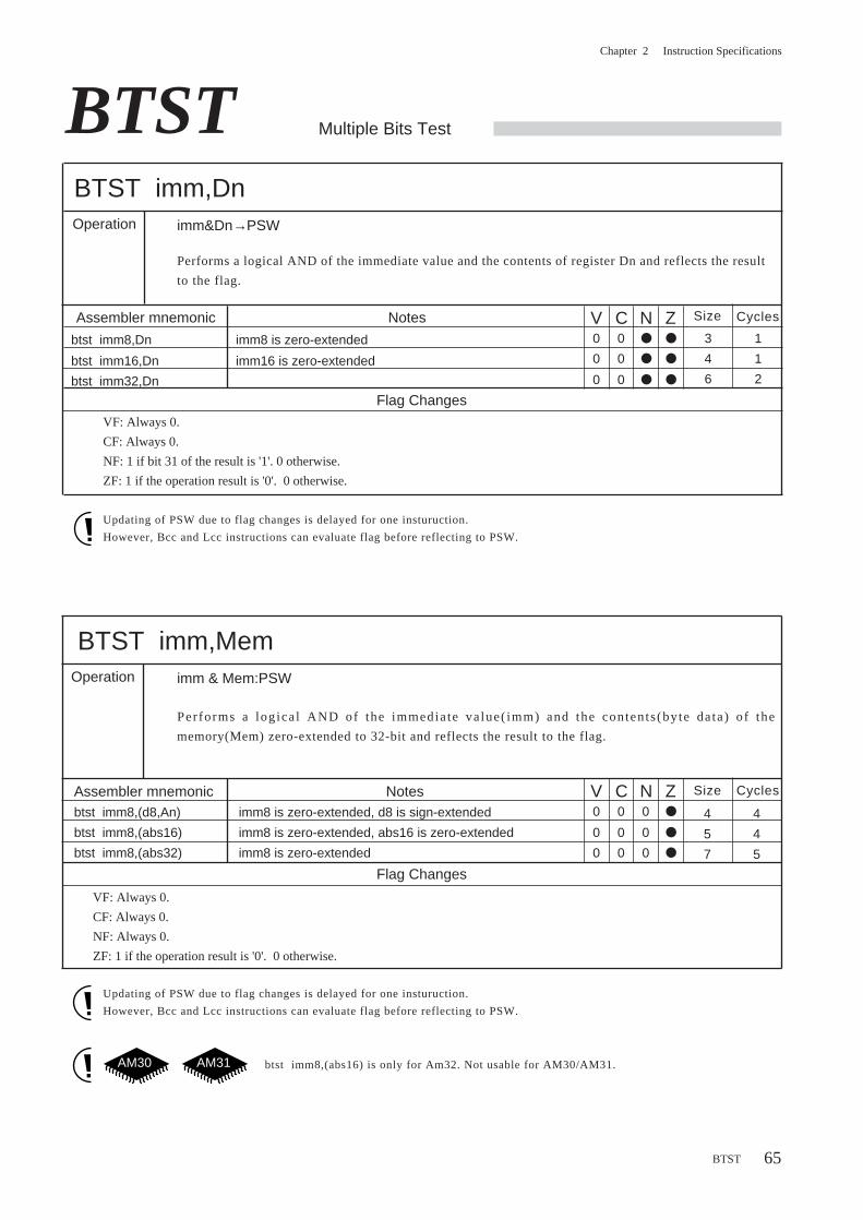
Chapter 2 Instruction Specifications
65
BTST Multiple Bits Test
BTST imm,Dn
V C Z
Operation imm&Dn→PSW
Performs a logical AND of the immediate value and the contents of register Dn and reflects the result
to the flag.
N
BTST imm,MemOperation imm & Mem:PSW
Assembler mnemonic Size Cycles
btst imm8,Dn imm8 is zero-extended
btst imm16,Dn imm16 is zero-extended
btst imm32,Dn
Notes3
4
6
1
1
2
Updating of PSW due to flag changes is delayed for one insturuction.
However, Bcc and Lcc instructions can evaluate flag before reflecting to PSW.
Flag Changes
VF: Always 0.
CF: Always 0.
NF: 1 if bit 31 of the result is '1'. 0 otherwise.
ZF: 1 if the operation result is '0'. 0 otherwise.
Assembler mnemonic
Performs a log ica l AND of the immediate value( imm) and the contents(byte data) of the
memory(Mem) zero-extended to 32-bit and reflects the result to the flag.
Size Cycles
btst imm8,(d8,An) imm8 is zero-extended, d8 is sign-extended
btst imm8,(abs16) imm8 is zero-extended, abs16 is zero-extended
btst imm8,(abs32) imm8 is zero-extended
Notes
4
5
7
4
4
5
BTST
0
0
0
0
0
0
●
●
●
●
●
●
V C ZN0
0
0
0
0
0
0
0
0
●
●
●
Bit
Man
ipul
a-
tion
Inst
ruct
ion
Updating of PSW due to flag changes is delayed for one insturuction.
However, Bcc and Lcc instructions can evaluate flag before reflecting to PSW.
Flag Changes
VF: Always 0.
CF: Always 0.
NF: Always 0.
ZF: 1 if the operation result is '0'. 0 otherwise.
btst imm8,(abs16) is only for Am32. Not usable for AM30/AM31.AM30 AM31
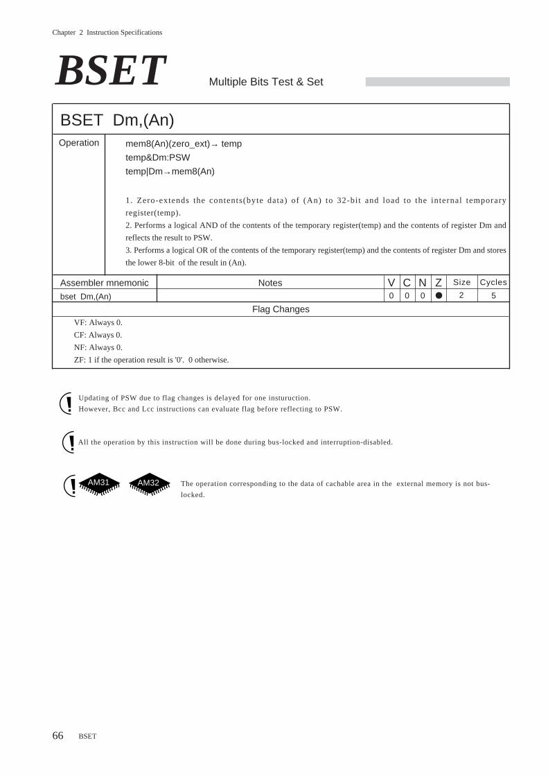
Chapter 2 Instruction Specifications
66
BSET Multiple Bits Test & Set
BSET Dm,(An)Operation mem8(An)(zero_ext)→ temp
temp&Dm:PSW
temp|Dm→mem8(An)
1. Zero-extends the contents(byte data) of (An) to 32-bit and load to the internal temporary
register(temp).
2. Performs a logical AND of the contents of the temporary register(temp) and the contents of register Dm and
reflects the result to PSW.
3. Performs a logical OR of the contents of the temporary register(temp) and the contents of register Dm and stores
the lower 8-bit of the result in (An).
Updating of PSW due to flag changes is delayed for one insturuction.
However, Bcc and Lcc instructions can evaluate flag before reflecting to PSW.
Flag ChangesVF: Always 0.
CF: Always 0.
NF: Always 0.
ZF: 1 if the operation result is '0'. 0 otherwise.
Assembler mnemonic Size Cycles
bset Dm,(An)
Notes5
All the operation by this instruction will be done during bus-locked and interruption-disabled.
BSET
V C ZN0 0 0 ●
The operation corresponding to the data of cachable area in the external memory is not bus-
locked.
AM31 AM32
2
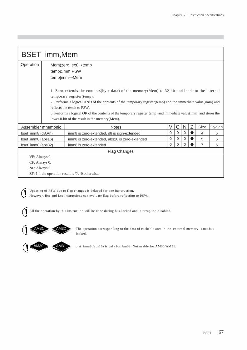
Chapter 2 Instruction Specifications
67
BSET imm,MemOperation Mem(zero_ext)→temp
temp&imm:PSW
temp|imm→Mem
1. Zero-extends the contents(byte data) of the memory(Mem) to 32-bit and loads to the internal
temporary register(temp).
2. Performs a logical AND of the contents of the temporary register(temp) and the immediate value(imm) and
reflects the result to PSW.
3. Performs a logical OR of the contents of the temporary register(temp) and immediate value(imm) and stores the
lower 8-bit of the result in the memory(Mem).
Assembler mnemonic Size Cycles
bset imm8,(d8,An) imm8 is zero-extended, d8 is sign-extended
bset imm8,(abs16) imm8 is zero-extended, abs16 is zero-extended
bset imm8,(abs32) imm8 is zero-extended
Notes4
5
7
5
5
6
BSET
V C ZN0
0
0
0
0
0
0
0
0
●
●
●
Flag ChangesVF: Always 0.
CF: Always 0.
NF: Always 0.
ZF: 1 if the operation result is '0'. 0 otherwise.
Updating of PSW due to flag changes is delayed for one insturuction.
However, Bcc and Lcc instructions can evaluate flag before reflecting to PSW.
All the operation by this instruction will be done during bus-locked and interruption-disabled.
The operation corresponding to the data of cachable area in the external memory is not bus-
locked.
AM31 AM32
btst imm8,(abs16) is only for Am32. Not usable for AM30/AM31.AM30 AM31
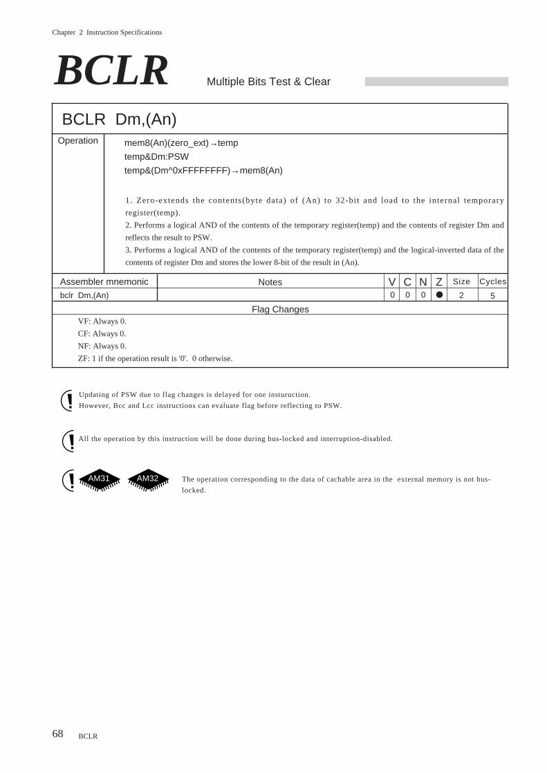
Chapter 2 Instruction Specifications
68
BCLR Multiple Bits Test & Clear
BCLR Dm,(An)Operation mem8(An)(zero_ext)→temp
temp&Dm:PSW
temp&(Dm^0xFFFFFFFF)→mem8(An)
1. Zero-extends the contents(byte data) of (An) to 32-bit and load to the internal temporary
register(temp).
2. Performs a logical AND of the contents of the temporary register(temp) and the contents of register Dm and
reflects the result to PSW.
3. Performs a logical AND of the contents of the temporary register(temp) and the logical-inverted data of the
contents of register Dm and stores the lower 8-bit of the result in (An).
Flag ChangesVF: Always 0.
CF: Always 0.
NF: Always 0.
ZF: 1 if the operation result is '0'. 0 otherwise.
Assembler mnemonic Size Cycles
bclr Dm,(An)
Notes2 5
BCLR
V C ZN0 0 0 ●
All the operation by this instruction will be done during bus-locked and interruption-disabled.
Updating of PSW due to flag changes is delayed for one insturuction.
However, Bcc and Lcc instructions can evaluate flag before reflecting to PSW.
The operation corresponding to the data of cachable area in the external memory is not bus-
locked.
AM31 AM32
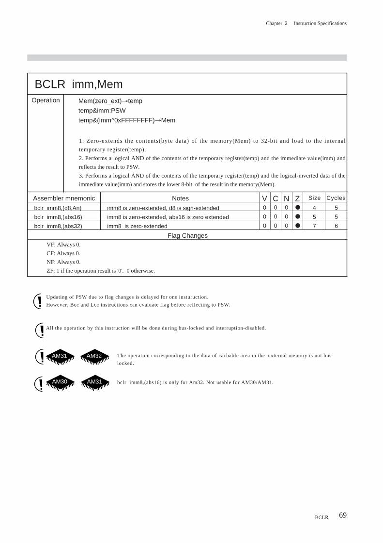
Chapter 2 Instruction Specifications
69
BCLR imm,MemOperation Mem(zero_ext)→temp
temp&imm:PSW
temp&(imm^0xFFFFFFFF)→Mem
1. Zero-extends the contents(byte data) of the memory(Mem) to 32-bit and load to the internal
temporary register(temp).
2. Performs a logical AND of the contents of the temporary register(temp) and the immediate value(imm) and
reflects the result to PSW.
3. Performs a logical AND of the contents of the temporary register(temp) and the logical-inverted data of the
immediate value(imm) and stores the lower 8-bit of the result in the memory(Mem).
Assembler mnemonic Size Cycles
bclr imm8,(d8,An) imm8 is zero-extended, d8 is sign-extended
bclr imm8,(abs16) imm8 is zero-extended, abs16 is zero extended
bclr imm8,(abs32) imm8 is zero-extended
Notes4
5
7
5
5
6
BCLR
V C ZN0
0
0
0
0
0
0
0
0
●
●
●
bclr imm8,(abs16) is only for Am32. Not usable for AM30/AM31.AM30 AM31
Flag ChangesVF: Always 0.
CF: Always 0.
NF: Always 0.
ZF: 1 if the operation result is '0'. 0 otherwise.
Updating of PSW due to flag changes is delayed for one insturuction.
However, Bcc and Lcc instructions can evaluate flag before reflecting to PSW.
All the operation by this instruction will be done during bus-locked and interruption-disabled.
The operation corresponding to the data of cachable area in the external memory is not bus-
locked.AM31 AM32
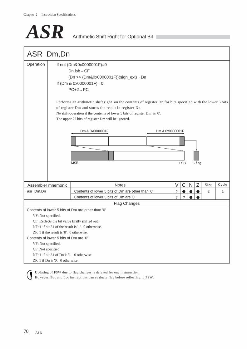
Chapter 2 Instruction Specifications
70
ASR Arithmetic Shift Right for Optional Bit
ASR Dm,Dn
V C Z
Operation
N
If not (Dm&0x0000001F)=0
Dn.lsb→CF
(Dn >> (Dm&0x0000001F))(sign_ext)→Dn
If (Dm & 0x0000001F) =0
PC+2→PC
Performs an arithmetic shift right on the contents of register Dn for bits specified with the lower 5 bits
of register Dm and stores the result in register Dn.
No shift-operation if the contents of lower 5 bits of register Dm is '0'.
The upper 27 bits of register Dm will be ignored.
Updating of PSW due to flag changes is delayed for one insturuction.
However, Bcc and Lcc instructions can evaluate flag before reflecting to PSW.
Flag Changes
Contents of lower 5 bits of Dm are other than '0'
VF: Not specified.
CF: Reflects the bit value firstly shifted out.
NF: 1 if bit 31 of the result is '1'. 0 otherwise.
ZF: 1 if the result is '0'. 0 otherwise.
Contents of lower 5 bits of Dm are '0'
VF: Not specified.
CF: Not specified.
NF: 1 if bit 31 of Dn is '1'. 0 otherwise.
ZF: 1 if Dn is '0'. 0 otherwise.
Assembler mnemonic Size Cycle
asr Dm,Dn Contents of lower 5 bits of Dm are other than '0'
Contents of lower 5 bits of Dm are '0'
Notes
2 1
ASR
?
?
●
?
●
●
●
●
Dm & 0x0000001F
MSB LSB C flag
Dm & 0x0000001F
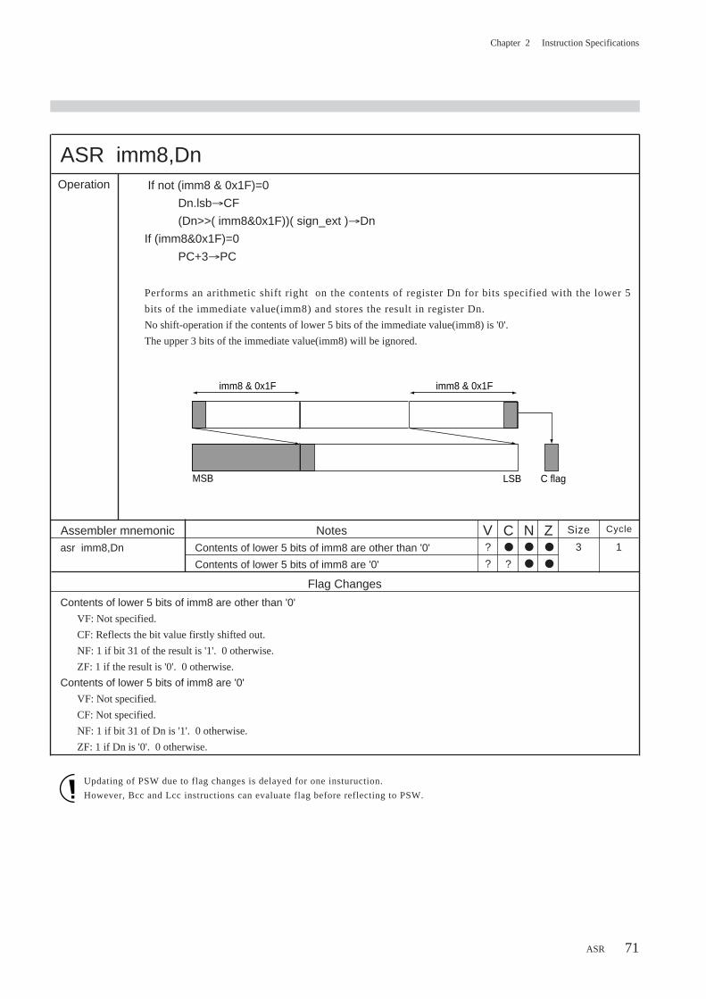
Chapter 2 Instruction Specifications
71
ASR
ASR imm8,DnOperation If not (imm8 & 0x1F)=0
Dn.lsb→CF
(Dn>>( imm8&0x1F))( sign_ext )→Dn
If (imm8&0x1F)=0
PC+3→PC
Performs an arithmetic shift right on the contents of register Dn for bits specified with the lower 5
bits of the immediate value(imm8) and stores the result in register Dn.
No shift-operation if the contents of lower 5 bits of the immediate value(imm8) is '0'.
The upper 3 bits of the immediate value(imm8) will be ignored.
Updating of PSW due to flag changes is delayed for one insturuction.
However, Bcc and Lcc instructions can evaluate flag before reflecting to PSW.
Flag Changes
Contents of lower 5 bits of imm8 are other than '0'
VF: Not specified.
CF: Reflects the bit value firstly shifted out.
NF: 1 if bit 31 of the result is '1'. 0 otherwise.
ZF: 1 if the result is '0'. 0 otherwise.
Contents of lower 5 bits of imm8 are '0'
VF: Not specified.
CF: Not specified.
NF: 1 if bit 31 of Dn is '1'. 0 otherwise.
ZF: 1 if Dn is '0'. 0 otherwise.
Assembler mnemonic Size Cycle
asr imm8,Dn Contents of lower 5 bits of imm8 are other than '0'
Contents of lower 5 bits of imm8 are '0'
Notes3 1
ASR
V C ZN?
?
●
?
●
●
●
●
imm8 & 0x1F
MSB LSB C flag
imm8 & 0x1F
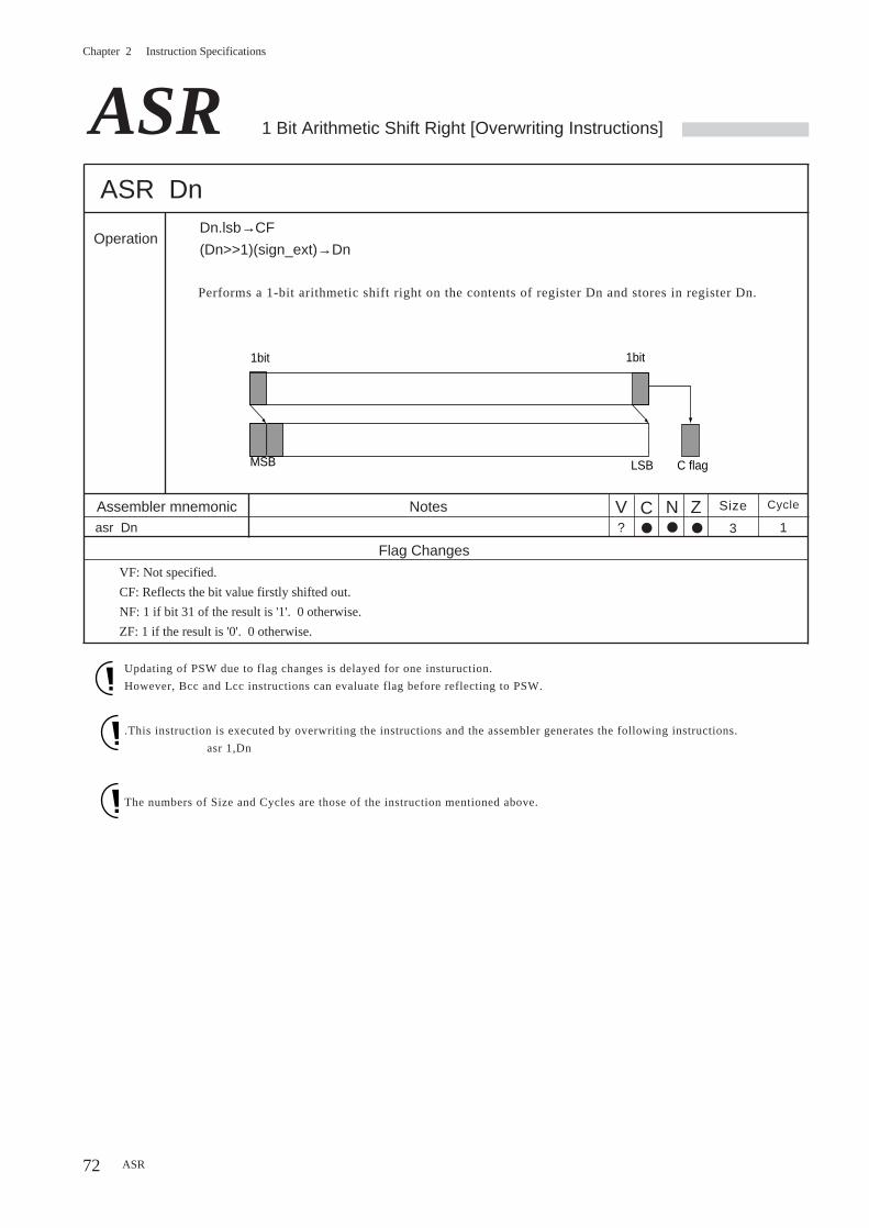
Chapter 2 Instruction Specifications
72
ASR Dn
OperationDn.lsb→CF
(Dn>>1)(sign_ext)→Dn
Performs a 1-bit arithmetic shift right on the contents of register Dn and stores in register Dn.
Updating of PSW due to flag changes is delayed for one insturuction.
However, Bcc and Lcc instructions can evaluate flag before reflecting to PSW.
Flag Changes
VF: Not specified.
CF: Reflects the bit value firstly shifted out.
NF: 1 if bit 31 of the result is '1'. 0 otherwise.
ZF: 1 if the result is '0'. 0 otherwise.
Assembler mnemonic Size Cycle
asr Dn
Notes
3 1
.This instruction is executed by overwriting the instructions and the assembler generates the following instructions.
asr 1,Dn
ASR
ASR 1 Bit Arithmetic Shift Right [Overwriting Instructions]
The numbers of Size and Cycles are those of the instruction mentioned above.
V C ZN? ● ● ●
1bit
MSB LSB C flag
1bit
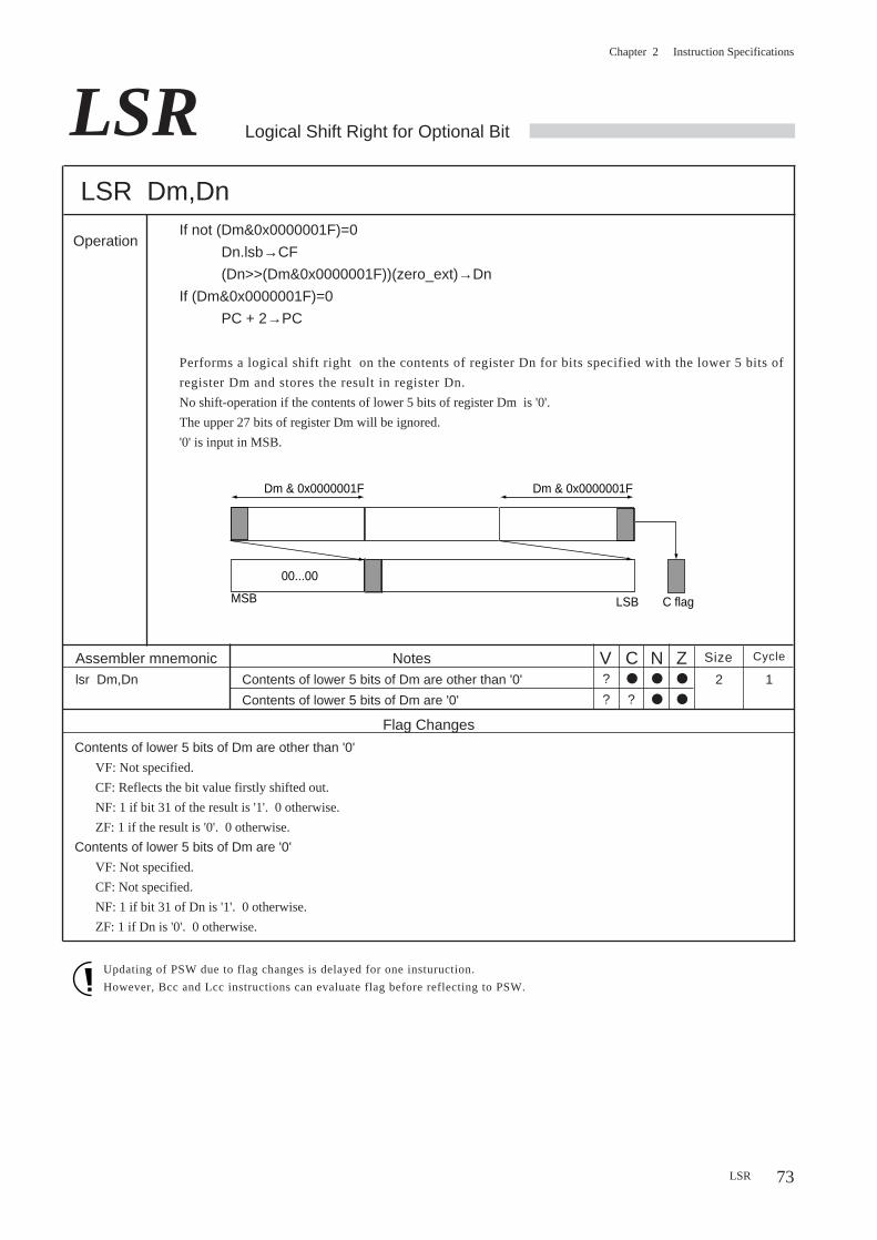
Chapter 2 Instruction Specifications
73
LSR
AS
R
Logical Shift Right for Optional Bit
LSR Dm,Dn
OperationIf not (Dm&0x0000001F)=0
Dn.lsb→CF
(Dn>>(Dm&0x0000001F))(zero_ext)→Dn
If (Dm&0x0000001F)=0
PC + 2→PC
Performs a logical shift right on the contents of register Dn for bits specified with the lower 5 bits of
register Dm and stores the result in register Dn.
No shift-operation if the contents of lower 5 bits of register Dm is '0'.
The upper 27 bits of register Dm will be ignored.
'0' is input in MSB.
Updating of PSW due to flag changes is delayed for one insturuction.
However, Bcc and Lcc instructions can evaluate flag before reflecting to PSW.
Flag Changes
Contents of lower 5 bits of Dm are other than '0'
VF: Not specified.
CF: Reflects the bit value firstly shifted out.
NF: 1 if bit 31 of the result is '1'. 0 otherwise.
ZF: 1 if the result is '0'. 0 otherwise.
Contents of lower 5 bits of Dm are '0'
VF: Not specified.
CF: Not specified.
NF: 1 if bit 31 of Dn is '1'. 0 otherwise.
ZF: 1 if Dn is '0'. 0 otherwise.
Assembler mnemonic Size Cycle
lsr Dm,Dn Contents of lower 5 bits of Dm are other than '0'
Contents of lower 5 bits of Dm are '0'
Notes2 1
LSR
LSR
V C ZN?
?
●
?
●
●
●
●
Dm & 0x0000001F
MSB LSB C flag
00...00
Dm & 0x0000001F
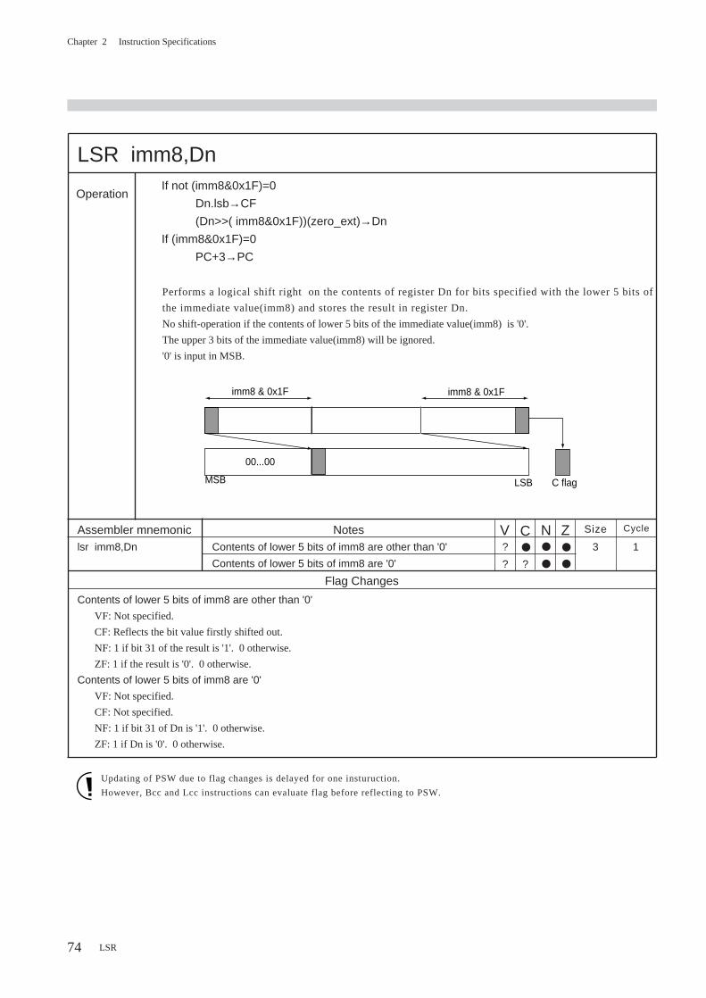
Chapter 2 Instruction Specifications
74
LSR
LSR imm8,Dn
OperationIf not (imm8&0x1F)=0
Dn.lsb→CF
(Dn>>( imm8&0x1F))(zero_ext)→Dn
If (imm8&0x1F)=0
PC+3→PC
Performs a logical shift right on the contents of register Dn for bits specified with the lower 5 bits of
the immediate value(imm8) and stores the result in register Dn.
No shift-operation if the contents of lower 5 bits of the immediate value(imm8) is '0'.
The upper 3 bits of the immediate value(imm8) will be ignored.
'0' is input in MSB.
Updating of PSW due to flag changes is delayed for one insturuction.
However, Bcc and Lcc instructions can evaluate flag before reflecting to PSW.
Flag Changes
Contents of lower 5 bits of imm8 are other than '0'
VF: Not specified.
CF: Reflects the bit value firstly shifted out.
NF: 1 if bit 31 of the result is '1'. 0 otherwise.
ZF: 1 if the result is '0'. 0 otherwise.
Contents of lower 5 bits of imm8 are '0'
VF: Not specified.
CF: Not specified.
NF: 1 if bit 31 of Dn is '1'. 0 otherwise.
ZF: 1 if Dn is '0'. 0 otherwise.
Assembler mnemonic Size Cycle
lsr imm8,Dn Contents of lower 5 bits of imm8 are other than '0'
Contents of lower 5 bits of imm8 are '0'
Notes3 1
LSR
V C ZN?
?
●
?
●
●
●
●
imm8 & 0x1F imm8 & 0x1F
MSB LSB C flag
00...00
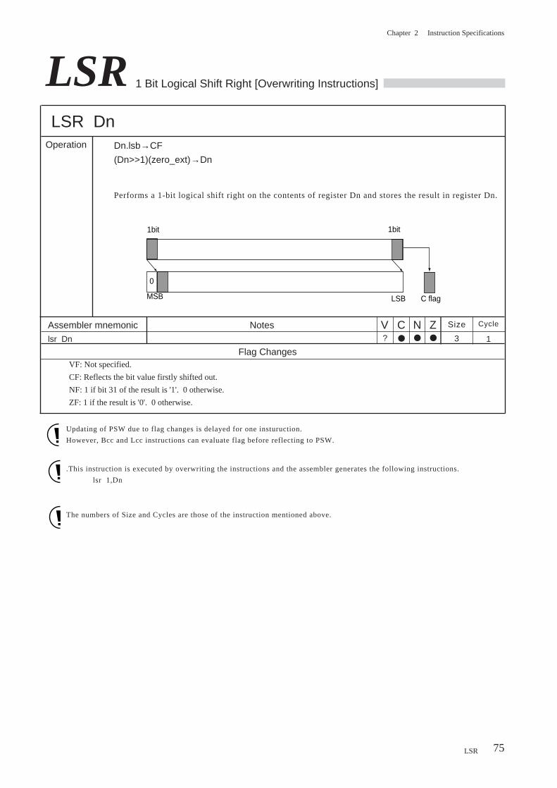
Chapter 2 Instruction Specifications
75
LSR DnOperation Dn.lsb→CF
(Dn>>1)(zero_ext)→Dn
Performs a 1-bit logical shift right on the contents of register Dn and stores the result in register Dn.
Updating of PSW due to flag changes is delayed for one insturuction.
However, Bcc and Lcc instructions can evaluate flag before reflecting to PSW.
Flag ChangesVF: Not specified.
CF: Reflects the bit value firstly shifted out.
NF: 1 if bit 31 of the result is '1'. 0 otherwise.
ZF: 1 if the result is '0'. 0 otherwise.
Assembler mnemonic Size Cycle
lsr Dn
Notes3 1
.This instruction is executed by overwriting the instructions and the assembler generates the following instructions.
lsr 1,Dn
LSR
LSR 1 Bit Logical Shift Right [Overwriting Instructions]
The numbers of Size and Cycles are those of the instruction mentioned above.
V C ZN? ● ● ●
1bit
MSB LSB C flag
1bit
0
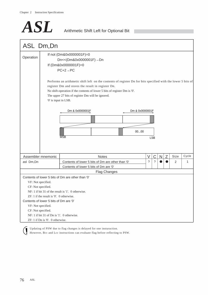
Chapter 2 Instruction Specifications
76
ASL Arithmetic Shift Left for Optional Bit
ASL Dm,Dn
OperationIf not (Dm&0x0000001F)=0
Dn<<(Dm&0x0000001F)→Dn
If (Dm&0x0000001F)=0
PC+2→PC
Performs an arithmetic shift left on the contents of register Dn for bits specified with the lower 5 bits of
register Dm and stores the result in register Dn.
No shift-operation if the contents of lower 5 bits of register Dm is '0'.
The upper 27 bits of register Dm will be ignored.
'0' is input in LSB.
Updating of PSW due to flag changes is delayed for one insturuction.
However, Bcc and Lcc instructions can evaluate flag before reflecting to PSW.
Flag Changes
Contents of lower 5 bits of Dm are other than '0'
VF: Not specified.
CF: Not specified.
NF: 1 if bit 31 of the result is '1'. 0 otherwise.
ZF: 1 if the result is '0'. 0 otherwise.
Contents of lower 5 bits of Dm are '0'
VF: Not specified.
CF: Not specified.
NF: 1 if bit 31 of Dn is '1'. 0 otherwise.
ZF: 1 if Dn is '0'. 0 otherwise.
Assembler mnemonic Size Cycle
asl Dm,Dn Contents of lower 5 bits of Dm are other than '0'
Contents of lower 5 bits of Dm are '0'
Notes
2 1
ASL
V C ZN? ? ● ●
Dm & 0x0000001F
MSB LSB
00...00
Dm & 0x0000001F
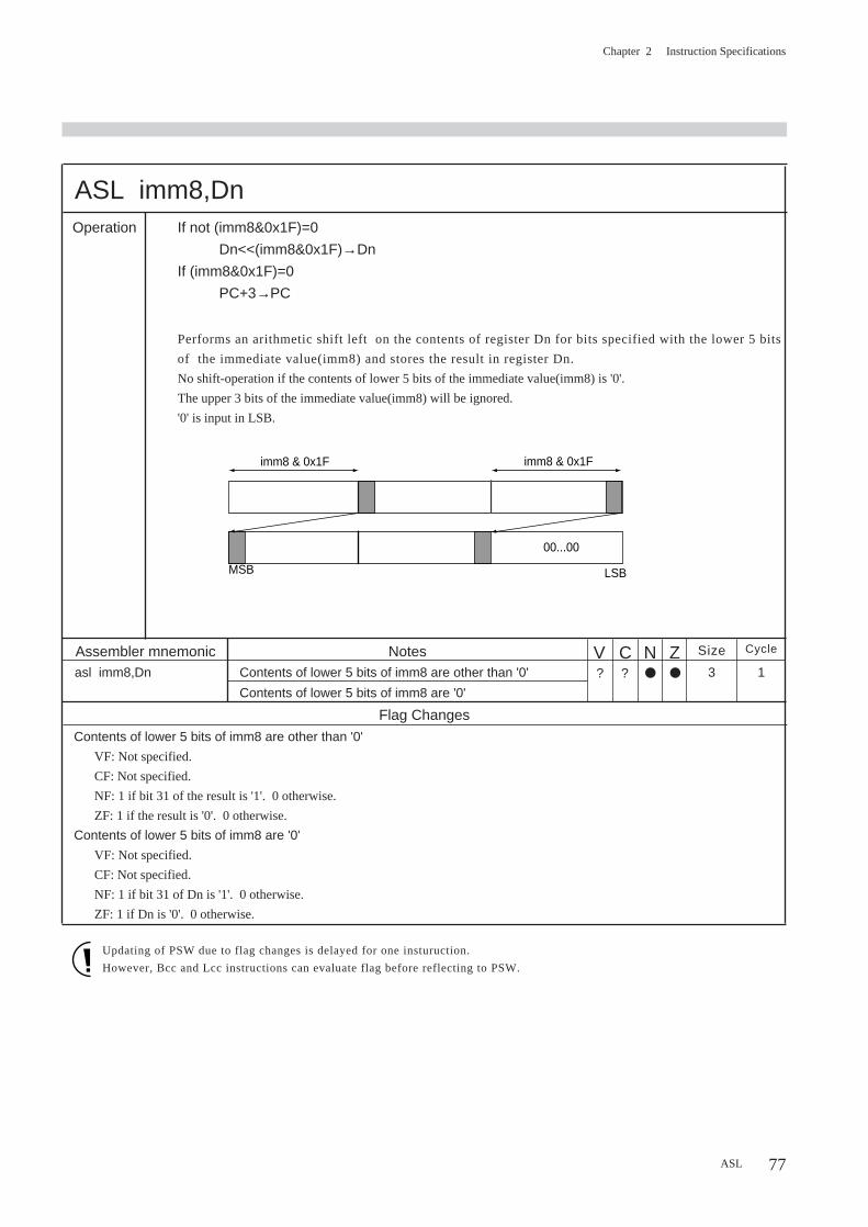
Chapter 2 Instruction Specifications
77
ASL imm8,DnOperation If not (imm8&0x1F)=0
Dn<<(imm8&0x1F)→Dn
If (imm8&0x1F)=0
PC+3→PC
Performs an arithmetic shift left on the contents of register Dn for bits specified with the lower 5 bits
of the immediate value(imm8) and stores the result in register Dn.
No shift-operation if the contents of lower 5 bits of the immediate value(imm8) is '0'.
The upper 3 bits of the immediate value(imm8) will be ignored.
'0' is input in LSB.
Updating of PSW due to flag changes is delayed for one insturuction.
However, Bcc and Lcc instructions can evaluate flag before reflecting to PSW.
Flag Changes
Contents of lower 5 bits of imm8 are other than '0'
VF: Not specified.
CF: Not specified.
NF: 1 if bit 31 of the result is '1'. 0 otherwise.
ZF: 1 if the result is '0'. 0 otherwise.
Contents of lower 5 bits of imm8 are '0'
VF: Not specified.
CF: Not specified.
NF: 1 if bit 31 of Dn is '1'. 0 otherwise.
ZF: 1 if Dn is '0'. 0 otherwise.
Assembler mnemonic Size Cycle
asl imm8,Dn Contents of lower 5 bits of imm8 are other than '0'
Contents of lower 5 bits of imm8 are '0'
Notes3 1
ASL
V C ZN? ? ● ●
imm8 & 0x1F imm8 & 0x1F
MSB LSB
00...00
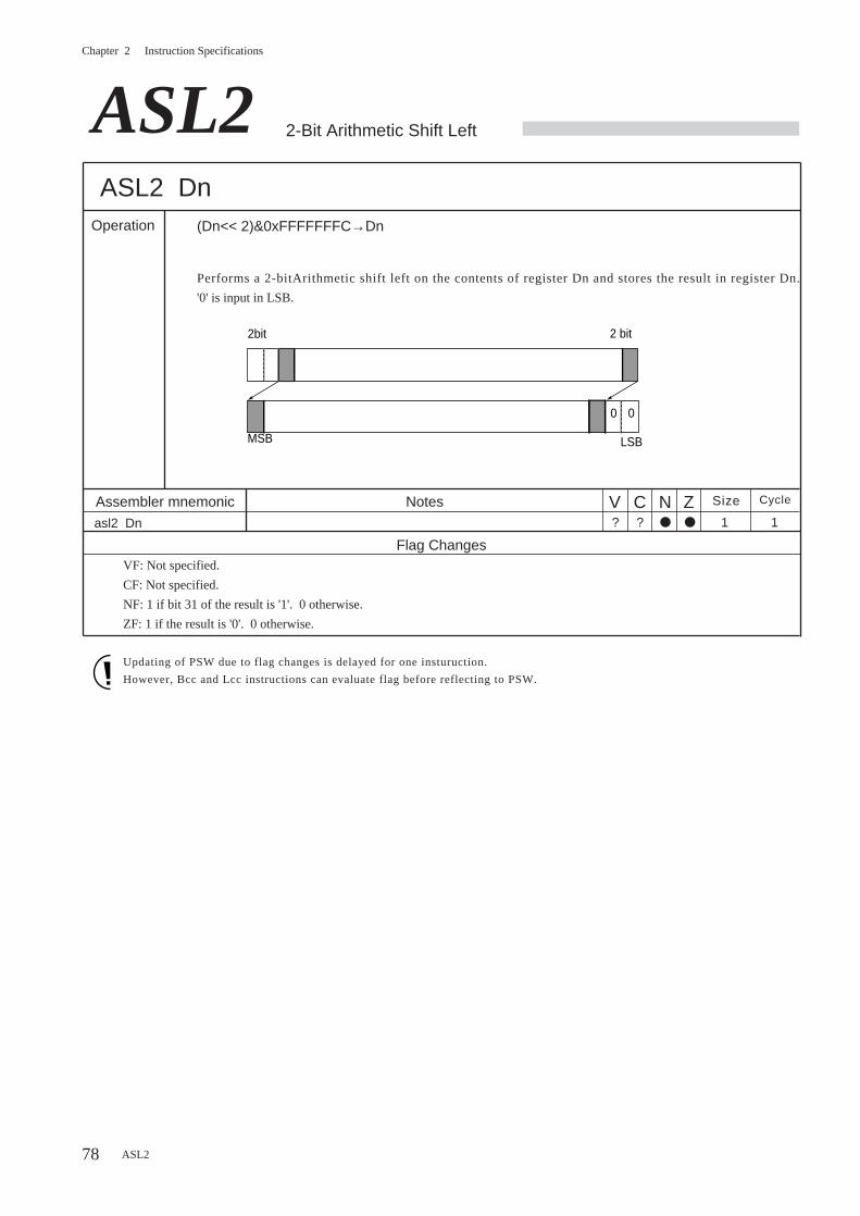
Chapter 2 Instruction Specifications
78
ASL2 2-Bit Arithmetic Shift Left
ASL2 DnOperation (Dn<< 2)&0xFFFFFFFC→Dn
Performs a 2-bitArithmetic shift left on the contents of register Dn and stores the result in register Dn.
'0' is input in LSB.
Updating of PSW due to flag changes is delayed for one insturuction.
However, Bcc and Lcc instructions can evaluate flag before reflecting to PSW.
Flag ChangesVF: Not specified.
CF: Not specified.
NF: 1 if bit 31 of the result is '1'. 0 otherwise.
ZF: 1 if the result is '0'. 0 otherwise.
Assembler mnemonic Size Cycle
asl2 Dn
Notes1 1
ASL2
V C ZN? ? ● ●
2bit 2 bit
MSB LSB
0 0
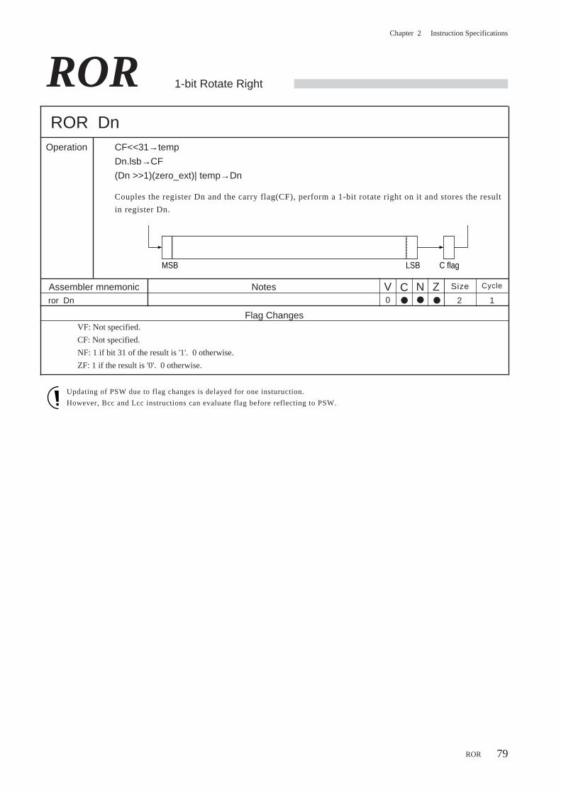
Chapter 2 Instruction Specifications
79
ROR 1-bit Rotate Right
ROR DnOperation CF<<31→temp
Dn.lsb→CF
(Dn >>1)(zero_ext)| temp→Dn
Couples the register Dn and the carry flag(CF), perform a 1-bit rotate right on it and stores the result
in register Dn.
Updating of PSW due to flag changes is delayed for one insturuction.
However, Bcc and Lcc instructions can evaluate flag before reflecting to PSW.
Flag ChangesVF: Not specified.
CF: Not specified.
NF: 1 if bit 31 of the result is '1'. 0 otherwise.
ZF: 1 if the result is '0'. 0 otherwise.
Assembler mnemonic Size Cycle
ror Dn
Notes2 1
ROR
V C ZN0 ● ● ●
MSB LSB C flag
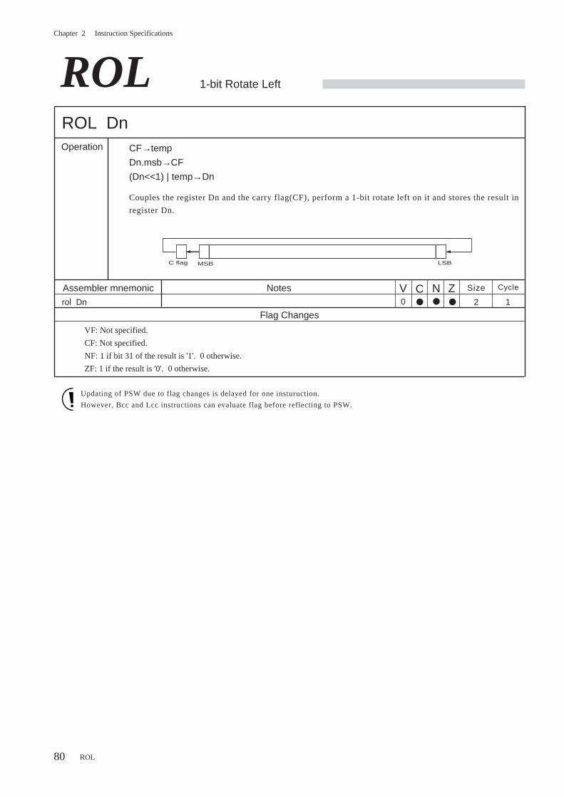
Chapter 2 Instruction Specifications
80
ROL 1-bit Rotate Left
ROL DnOperation CF→temp
Dn.msb→CF
(Dn<<1) | temp→Dn
Couples the register Dn and the carry flag(CF), perform a 1-bit rotate left on it and stores the result in
register Dn.
Updating of PSW due to flag changes is delayed for one insturuction.
However, Bcc and Lcc instructions can evaluate flag before reflecting to PSW.
Flag Changes
VF: Not specified.
CF: Not specified.
NF: 1 if bit 31 of the result is '1'. 0 otherwise.
ZF: 1 if the result is '0'. 0 otherwise.
Assembler mnemonic Size Cycle
rol Dn
Notes
2 1
ROL
V C ZN0 ● ● ●
C flag MSB LSB
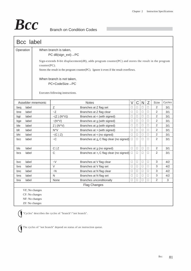
Chapter 2 Instruction Specifications
81
Bcc Branch on Condition Codes
Bcc label
V C Z
Operation When branch is taken,
PC d8(sign_ext)→PC
When branch is not taken,
PC+CodeSize→PC
Executes following instructions.
Sign-extends 8-bit displacement(d8), adds program counter(PC) and stores the result in the program
counter(PC).
Stores the result in the program counter(PC). Ignore it even if the result overflows.
N Size Cycles
beq label Z Branches at Z flag set
bne label ~Z Branches at Z flag clear
bgt label ~(Z | (N^V)) Branches at < (with signed)
bge label ~(N^V) Branches at ≤ (with signed)
ble label Z | (N^V) Branches at ≥ (with signed)
blt label N^V Branches at > (with signed)
bhi label ~(C | Z) Branches at < (no signed)
bcc label ~C Branches at ≤, C flag clear (no signed)
bls label C | Z Branches at ≥ (no signed)
bcs label C Branches at >, C flag clear (no signed)
bvc label ~V Branches at V flag clear
bvs label V Branches at V flag set
bnc label ~N Branches at N flag clear
bns label N Branches at N flag set
bra label None Branches unconditionally
Notes2
2
2
2
2
2
2
2
2
2
3
3
3
3
2
3/1
3/1
3/1
3/1
3/1
3/1
3/1
3/1
3/1
3/1
4/2
4/2
4/2
4/2
3
Assebler mnemonic
Bcc
Flag Changes
VF; No changes
CF: No changes
NF: No changes
ZF: No changes
"Cycles" describes the cycles of "branch"/"not branch".
The cycles of "not branch" depend on status of an instruction queue.
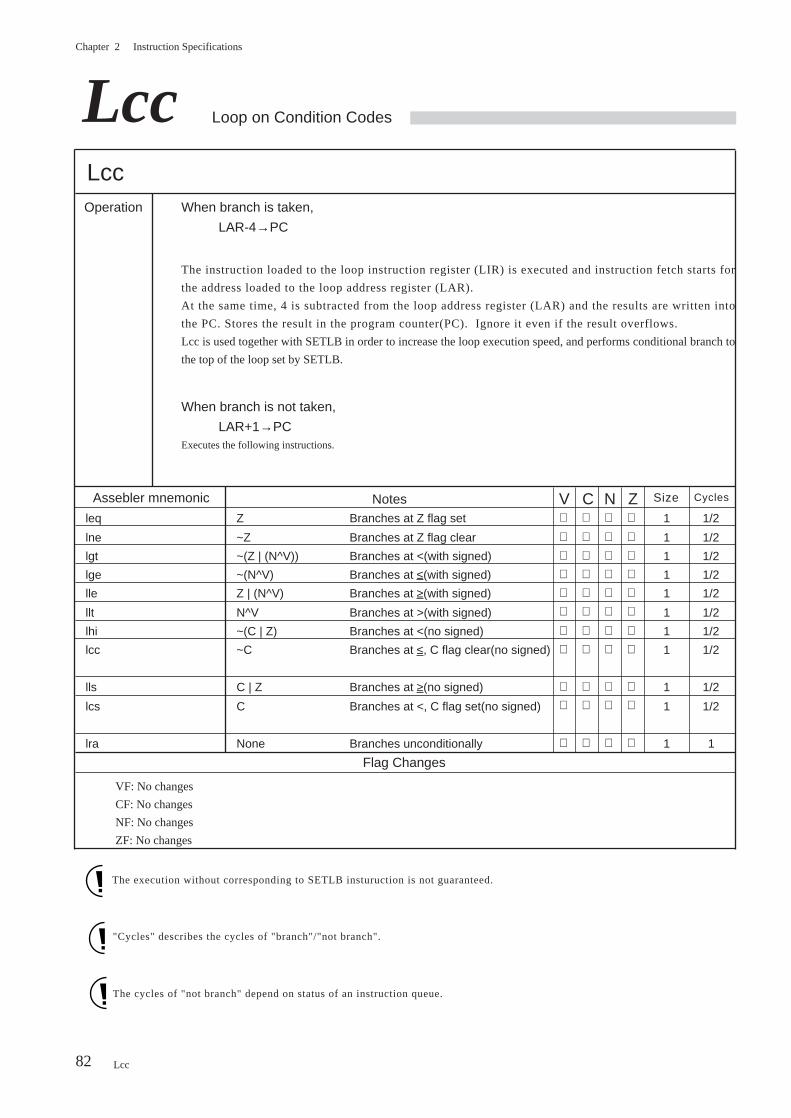
Chapter 2 Instruction Specifications
82
Lcc Loop on Condition Codes
LccOperation When branch is taken,
LAR-4→PC
When branch is not taken,
LAR+1→PCExecutes the following instructions.
The instruction loaded to the loop instruction register (LIR) is executed and instruction fetch starts for
the address loaded to the loop address register (LAR).
At the same time, 4 is subtracted from the loop address register (LAR) and the results are written into
the PC. Stores the result in the program counter(PC). Ignore it even if the result overflows.
Lcc is used together with SETLB in order to increase the loop execution speed, and performs conditional branch to
the top of the loop set by SETLB.
Lcc
Assebler mnemonic Size Cycles
leq Z Branches at Z flag set
lne ~Z Branches at Z flag clear
lgt ~(Z | (N^V)) Branches at <(with signed)
lge ~(N^V) Branches at ≤(with signed)
lle Z | (N^V) Branches at ≥(with signed)
llt N^V Branches at >(with signed)
lhi ~(C | Z) Branches at <(no signed)
lcc ~C Branches at ≤, C flag clear(no signed)
lls C | Z Branches at ≥(no signed)
lcs C Branches at <, C flag set(no signed)
lra None Branches unconditionally
Notes1
1
1
1
1
1
1
1
1
1
1
1/2
1/2
1/2
1/2
1/2
1/2
1/2
1/2
1/2
1/2
1
V C ZN
The execution without corresponding to SETLB insturuction is not guaranteed.
Flag Changes
VF: No changes
CF: No changes
NF: No changes
ZF: No changes
"Cycles" describes the cycles of "branch"/"not branch".
The cycles of "not branch" depend on status of an instruction queue.
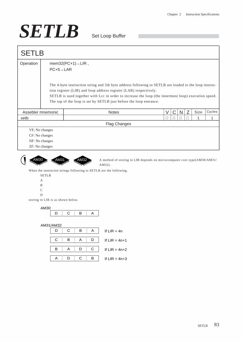
Chapter 2 Instruction Specifications
83
SETLB Set Loop Buffer
SETLBOperation mem32(PC+1)→LIR ,
PC+5→LAR
The 4-byte instruction string and 5th byte address following to SETLB are loaded to the loop instruc-
tion register (LIR) and loop address register (LAR) respectively.
SETLB is used together with Lcc in order to increase the loop (the innermost loop) execution speed.
The top of the loop is set by SETLB just before the loop entrance.
Flag Changes
VF; No changes
CF: No changes
NF: No changes
ZF: No changes
Assebler mnemonic Size Cycles
setlb
Notes1 1
SETLB
V C ZN
A method of storing in LIR depends on microcomputer core type(AM30/AM31/
AM32).
AM30 AM31 AM32
When the instrucion strings following to SETLB are the following,
SETLB
A
B
C
D
storing in LIR is as shown below.
D C B A
D C B A
C B A D
B A D C
A D C B
AM30
AM31/AM32
If LIR = 4n
If LIR = 4n+3
If LIR = 4n+1
If LIR = 4n+2
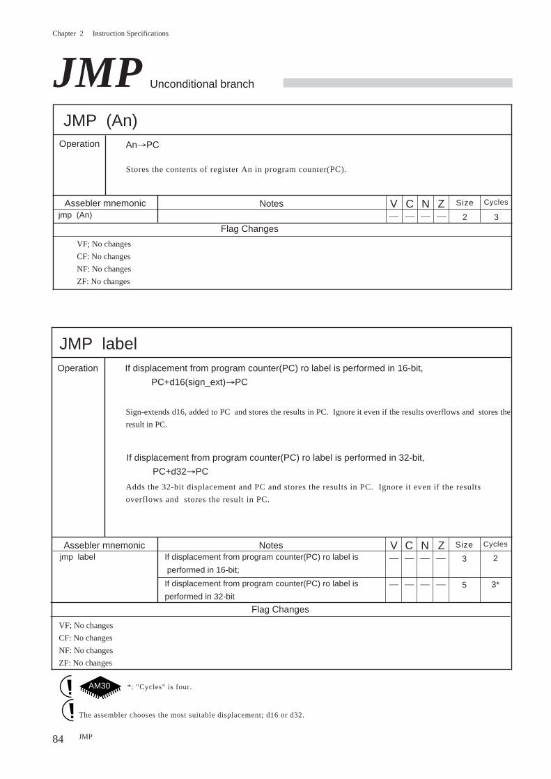
Chapter 2 Instruction Specifications
84
JMP Unconditional branch
JMP (An)
V C Z
Operation
N
An→PC
Stores the contents of register An in program counter(PC).
Flag Changes
VF; No changes
CF: No changes
NF: No changes
ZF: No changes
Assebler mnemonic Size Cycles
jmp (An)Notes
2 3
JMP labelOperation If displacement from program counter(PC) ro label is performed in 16-bit,
PC+d16(sign_ext)→PC
Sign-extends d16, added to PC and stores the results in PC. Ignore it even if the results overflows and stores the
result in PC.
Adds the 32-bit displacement and PC and stores the results in PC. Ignore it even if the results
overflows and stores the result in PC.
JMP
Assebler mnemonic Size Cycles
jmp label If displacement from program counter(PC) ro label is
performed in 16-bit;
If displacement from program counter(PC) ro label is
performed in 32-bit
Notes3
5
2
3*
If displacement from program counter(PC) ro label is performed in 32-bit,
PC+d32→PC
Flag Changes
VF; No changes
CF: No changes
NF: No changes
ZF: No changes
V C ZN
*: "Cycles" is four.AM30
The assembler chooses the most suitable displacement; d16 or d32.
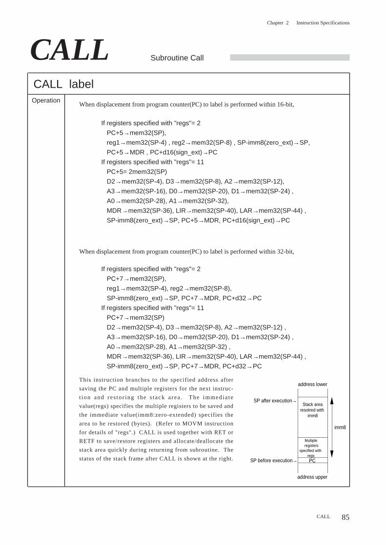
Chapter 2 Instruction Specifications
85
CALL labelOperation
CALL Subroutine Call
If registers specified with "regs"= 2
PC+5→mem32(SP),
reg1→mem32(SP-4) , reg2→mem32(SP-8) , SP-imm8(zero_ext)→SP,
PC+5→MDR , PC+d16(sign_ext)→PC
If registers specified with "regs"= 11
PC+5= 2mem32(SP)
D2→mem32(SP-4), D3→mem32(SP-8), A2→mem32(SP-12),
A3→mem32(SP-16), D0→mem32(SP-20), D1→mem32(SP-24) ,
A0→mem32(SP-28), A1→mem32(SP-32),
MDR→mem32(SP-36), LIR→mem32(SP-40), LAR→mem32(SP-44) ,
SP-imm8(zero_ext)→SP, PC+5→MDR, PC+d16(sign_ext)→PC
This instruction branches to the specified address after
saving the PC and multiple registers for the next instruc-
t ion and res to r ing the s tack area . The immedia te
value(regs) specifies the multiple registers to be saved and
the immediate value(imm8:zero-extended) specifies the
area to be restored (bytes). (Refer to MOVM instruction
for details of "regs".) CALL is used together with RET or
RETF to save/restore registers and allocate/deallocate the
stack area quickly during returning from subroutine. The
status of the stack frame after CALL is shown at the right.
CALL
If registers specified with "regs"= 2
PC+7→mem32(SP),
reg1→mem32(SP-4), reg2→mem32(SP-8),
SP-imm8(zero_ext)→SP, PC+7→MDR, PC+d32→PC
If registers specified with "regs"= 11
PC+7→mem32(SP)
D2→mem32(SP-4), D3→mem32(SP-8), A2→mem32(SP-12) ,
A3→mem32(SP-16), D0→mem32(SP-20), D1→mem32(SP-24) ,
A0→mem32(SP-28), A1→mem32(SP-32) ,
MDR→mem32(SP-36), LIR→mem32(SP-40), LAR→mem32(SP-44) ,
SP-imm8(zero_ext)→SP, PC+7→MDR, PC+d32→PC
When displacement from program counter(PC) to label is performed within 16-bit,
When displacement from program counter(PC) to label is performed within 32-bit,
SP before execution→
SP after execution→
address upper
address lower
PC
imm8
Stack arearesotred with
imm8
Multiple registers
specified with regs
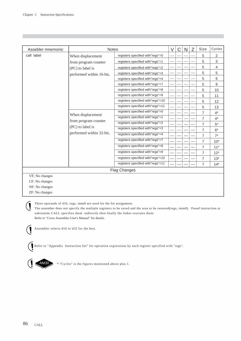
Chapter 2 Instruction Specifications
86 CALL
Three operands of d16, regs, imm8 are used for the bit assignment.
The assember does not specify the multiple registers to be saved and the area to be restored(regs, imm8). Pseud instruction at
subroutine CALL specifies them indirectly then finally the linker executes them.
Refer to "Cross Assembler User's Manual" for details.
Flag ChangesVF; No changes
CF: No changes
NF: No changes
ZF: No changes
Assebler mnemonic Size Cycles
call label registers specified with"regs"=0
registers specified with"regs"=1
registers specified with"regs"=2
registers specified with"regs"=3
registers specified with"regs"=4
registers specified with"regs"=7
registers specified with"regs"=8
registers specified with"regs"=9
registers specified with"regs"=10
registers specified with"regs"=11
registers specified with"regs"=0
registers specified with"regs"=1
registers specified with"regs"=2
registers specified with"regs"=3
registers specified with"regs"=4
registers specified with"regs"=7
registers specified with"regs"=8
registers specified with"regs"=9
registers specified with"regs"=10
registers specified with"regs"=11
Notes
5
5
5
5
5
5
5
5
5
5
7
7
7
7
7
7
7
7
7
7
2
3
4
5
6
9
10
11
12
13
4*
4*
5*
6*
7*
10*
11*
12*
13*
14*
Assembler selects d16 or d32 for the best.
V C ZN
When displacement
from program counter
(PC) to label is
performed within 16-bit,
When displacement
from program counter
(PC) to label is
performed within 32-bit,
Refer to "Appendix Instruction Set" for operation expressions by each register specified with "regs".
*:"Cycles" is the figures mentioned above plus 1.AM30
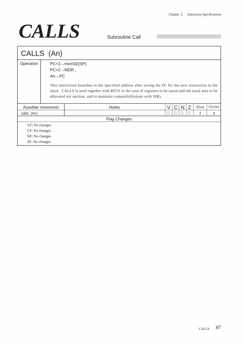
Chapter 2 Instruction Specifications
87
CALLS Subroutine Call
CALLS (An)
V C Z
Operation
N
PC+2→mem32(SP) .
PC+2→MDR ,
An→PC
This instruction branches to the specified address after saving the PC for the next instruction to the
stack. CALLS is used together with RETS in the case of registers to be saved and the stack area to be
allocated are unclear, and to maintain compatibility(use with JSR).
Flag Changes
VF; No changes
CF: No changes
NF: No changes
ZF: No changes
Assebler mnemonic Size Cycles
calls (An)
Notes2 3
CALLS
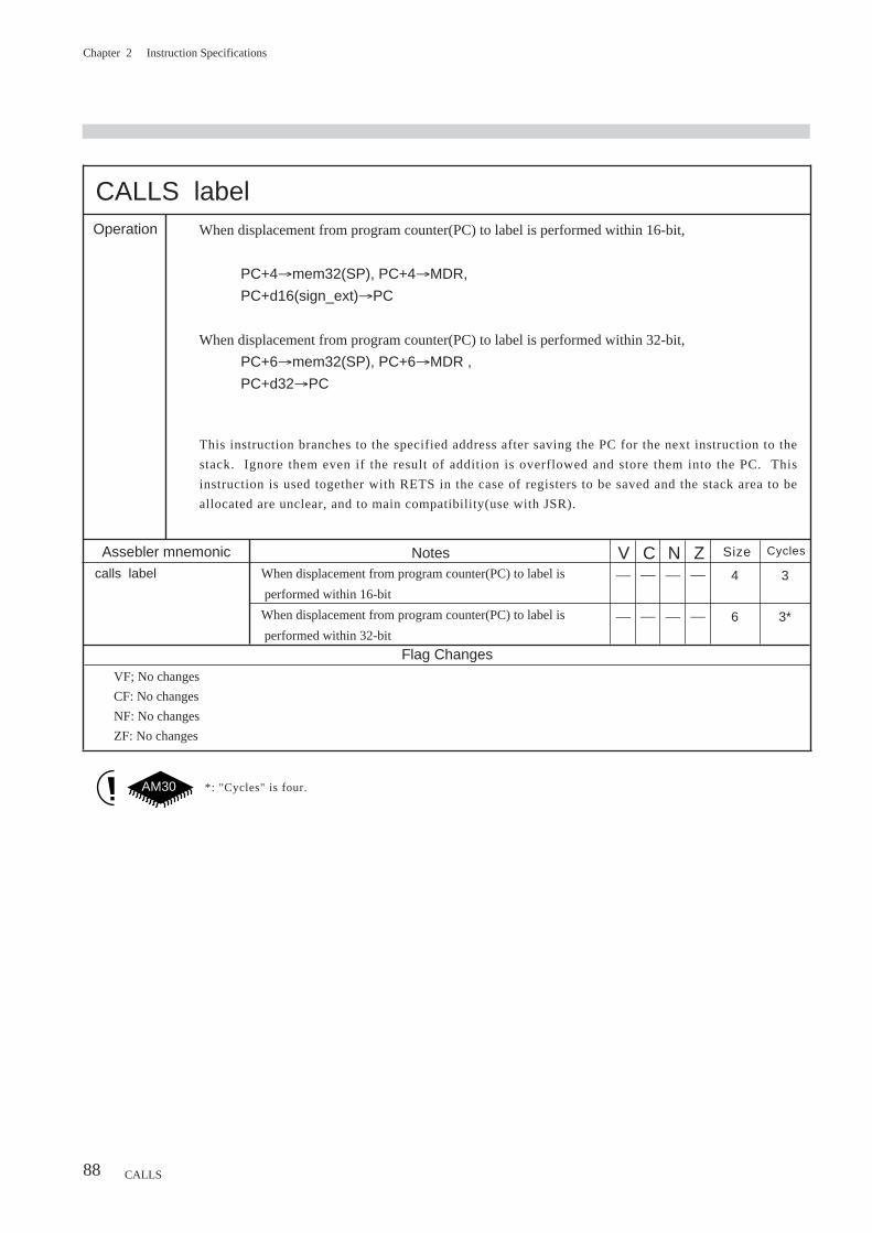
Chapter 2 Instruction Specifications
88 CALLS
CALLS labelOperation When displacement from program counter(PC) to label is performed within 16-bit,
PC+4→mem32(SP), PC+4→MDR,
PC+d16(sign_ext)→PC
When displacement from program counter(PC) to label is performed within 32-bit,
PC+6→mem32(SP), PC+6→MDR ,
PC+d32→PC
This instruction branches to the specified address after saving the PC for the next instruction to the
stack. Ignore them even if the result of addition is overflowed and store them into the PC. This
instruction is used together with RETS in the case of registers to be saved and the stack area to be
allocated are unclear, and to main compatibility(use with JSR).
Assebler mnemonic Size Cycles
calls label When displacement from program counter(PC) to label is
performed within 16-bit
When displacement from program counter(PC) to label is
performed within 32-bit
Notes
4
6
3
3*
V C ZN
Flag Changes
VF; No changes
CF: No changes
NF: No changes
ZF: No changes
*: "Cycles" is four.AM30
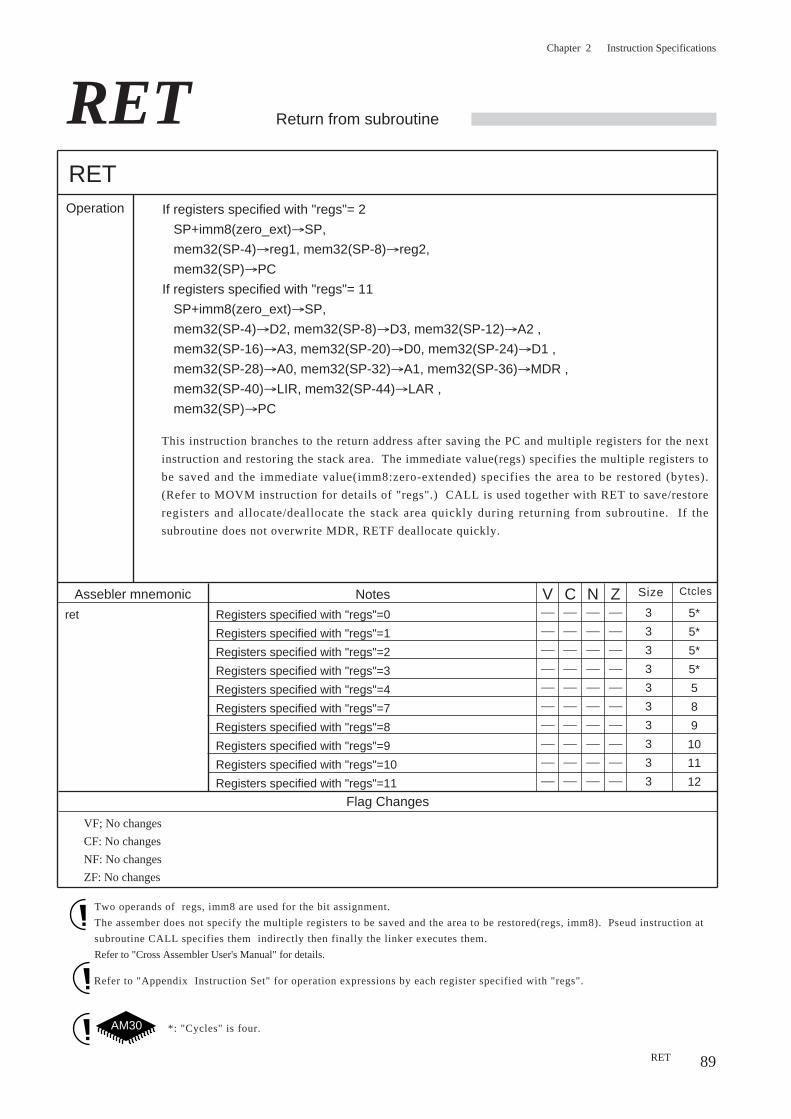
Chapter 2 Instruction Specifications
89
RET
V C Z
Operation
N
RET Return from subroutine
If registers specified with "regs"= 2
SP+imm8(zero_ext)→SP,
mem32(SP-4)→reg1, mem32(SP-8)→reg2,
mem32(SP)→PC
If registers specified with "regs"= 11
SP+imm8(zero_ext)→SP,
mem32(SP-4)→D2, mem32(SP-8)→D3, mem32(SP-12)→A2 ,
mem32(SP-16)→A3, mem32(SP-20)→D0, mem32(SP-24)→D1 ,
mem32(SP-28)→A0, mem32(SP-32)→A1, mem32(SP-36)→MDR ,
mem32(SP-40)→LIR, mem32(SP-44)→LAR ,
mem32(SP)→PC
This instruction branches to the return address after saving the PC and multiple registers for the next
instruction and restoring the stack area. The immediate value(regs) specifies the multiple registers to
be saved and the immediate value(imm8:zero-extended) specifies the area to be restored (bytes).
(Refer to MOVM instruction for details of "regs".) CALL is used together with RET to save/restore
registers and allocate/deallocate the stack area quickly during returning from subroutine. If the
subroutine does not overwrite MDR, RETF deallocate quickly.
Two operands of regs, imm8 are used for the bit assignment.
The assember does not specify the multiple registers to be saved and the area to be restored(regs, imm8). Pseud instruction at
subroutine CALL specifies them indirectly then finally the linker executes them.
Refer to "Cross Assembler User's Manual" for details.
Assebler mnemonic Size Ctcles
ret Registers specified with "regs"=0
Registers specified with "regs"=1
Registers specified with "regs"=2
Registers specified with "regs"=3
Registers specified with "regs"=4
Registers specified with "regs"=7
Registers specified with "regs"=8
Registers specified with "regs"=9
Registers specified with "regs"=10
Registers specified with "regs"=11
Notes3
3
3
3
3
3
3
3
3
3
5*
5*
5*
5*
5
8
9
10
11
12
Flag Changes
VF; No changes
CF: No changes
NF: No changes
ZF: No changes
Refer to "Appendix Instruction Set" for operation expressions by each register specified with "regs".
RET
*: "Cycles" is four.AM30
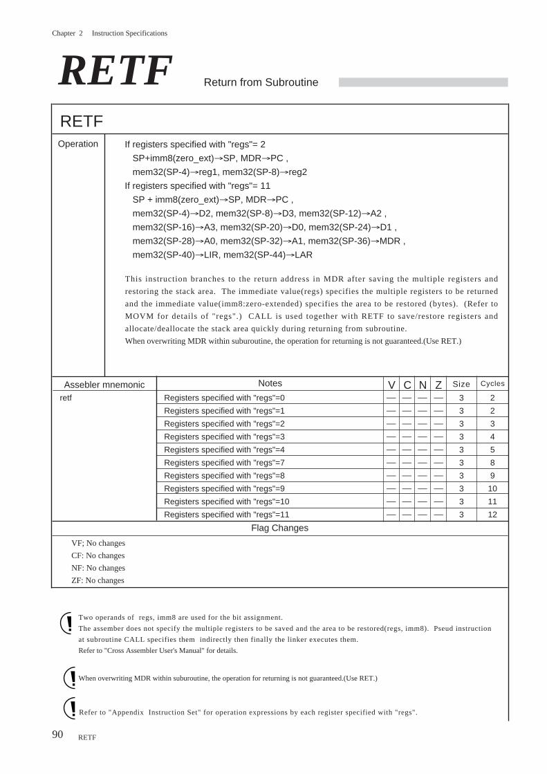
Chapter 2 Instruction Specifications
90
RETFRETF
This instruction branches to the return address in MDR after saving the multiple registers and
restoring the stack area. The immediate value(regs) specifies the multiple registers to be returned
and the immediate value(imm8:zero-extended) specifies the area to be restored (bytes). (Refer to
MOVM for details of "regs".) CALL is used together with RETF to save/restore registers and
allocate/deallocate the stack area quickly during returning from subroutine.
When overwriting MDR within suburoutine, the operation for returning is not guaranteed.(Use RET.)
V C Z
Operation
N
Return from Subroutine
If registers specified with "regs"= 2
SP+imm8(zero_ext)→SP, MDR→PC ,
mem32(SP-4)→reg1, mem32(SP-8)→reg2
If registers specified with "regs"= 11
SP + imm8(zero_ext)→SP, MDR→PC ,
mem32(SP-4)→D2, mem32(SP-8)→D3, mem32(SP-12)→A2 ,
mem32(SP-16)→A3, mem32(SP-20)→D0, mem32(SP-24)→D1 ,
mem32(SP-28)→A0, mem32(SP-32)→A1, mem32(SP-36)→MDR ,
mem32(SP-40)→LIR, mem32(SP-44)→LAR
Assebler mnemonic Size Cycles
retf Registers specified with "regs"=0
Registers specified with "regs"=1
Registers specified with "regs"=2
Registers specified with "regs"=3
Registers specified with "regs"=4
Registers specified with "regs"=7
Registers specified with "regs"=8
Registers specified with "regs"=9
Registers specified with "regs"=10
Registers specified with "regs"=11
Notes
3
3
3
3
3
3
3
3
3
3
2
2
3
4
5
8
9
10
11
12
Flag Changes
VF; No changes
CF: No changes
NF: No changes
ZF: No changes
Two operands of regs, imm8 are used for the bit assignment.
The assember does not specify the multiple registers to be saved and the area to be restored(regs, imm8). Pseud instruction
at subroutine CALL specifies them indirectly then finally the linker executes them.
Refer to "Cross Assembler User's Manual" for details.
When overwriting MDR within suburoutine, the operation for returning is not guaranteed.(Use RET.)
RETF
Refer to "Appendix Instruction Set" for operation expressions by each register specified with "regs".
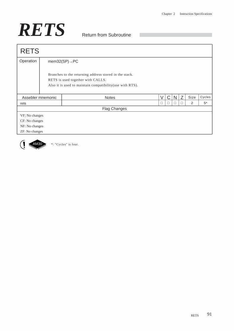
Chapter 2 Instruction Specifications
91
RETS Return from Subroutine
RETSOperation mem32(SP)→PC
Branches to the returning address stored in the stack.
RETS is used together with CALLS.
Also it is used to maintain compatibility(use with RTS).
Flag Changes
VF; No changes
CF: No changes
NF: No changes
ZF: No changes
Assebler mnemonic Size Cycles
rets
Notes2 5*
RETS
V C ZN
*: "Cycles" is four.AM30
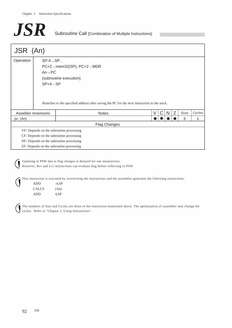
Chapter 2 Instruction Specifications
92
JSR Subroutine Call [Combination of Multiple Instructions]
JSR (An)Operation SP-4→SP ,
PC+2→mem32(SP), PC+2→MDR
An→PC
(subroutine execution)
SP+4→SP
Branches to the specified address after saving the PC for the next instruction to the stack.
Updating of PSW due to flag changes is delayed for one insturuction.
However, Bcc and Lcc instructions can evaluate flag before reflecting to PSW.
This instruction is executed by overwriting the instructions and the assembler generates the following instructions.
ADD -4,SP
CALLS (An)
ADD 4,SP
Flag Changes
VF: Depends on the subroutine processing
CF: Depends on the subroutine processing
NF: Depends on the subroutine processing
ZF: Depends on the subroutine processing
Assebler mnemonic Size Cycles
jsr (An)
Notes8 5
The numbers of Size and Cycles are those of the instruction mentioned above. The optimization of assembler may change the
cycles. Refer to "Chapter 3, Using Instructions".
V C ZN●●●●
JSR
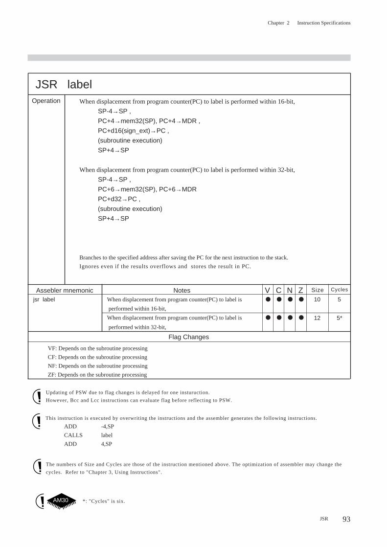
Chapter 2 Instruction Specifications
93
JSR labelOperation When displacement from program counter(PC) to label is performed within 16-bit,
SP-4→SP ,
PC+4→mem32(SP), PC+4→MDR ,
PC+d16(sign_ext)→PC ,
(subroutine execution)
SP+4→SP
When displacement from program counter(PC) to label is performed within 32-bit,
SP-4→SP ,
PC+6→mem32(SP), PC+6→MDR
PC+d32→PC ,
(subroutine execution)
SP+4→SP
JSR
Branches to the specified address after saving the PC for the next instruction to the stack.
Ignores even if the results overflows and stores the result in PC.
Assebler mnemonic Size Cycles
jsr label When displacement from program counter(PC) to label is
performed within 16-bit,
When displacement from program counter(PC) to label is
performed within 32-bit,
Notes10
12
5
5*
V C ZN●
●
●
●
●
●
●
●
This instruction is executed by overwriting the instructions and the assembler generates the following instructions.
ADD -4,SP
CALLS label
ADD 4,SP
Flag Changes
VF: Depends on the subroutine processing
CF: Depends on the subroutine processing
NF: Depends on the subroutine processing
ZF: Depends on the subroutine processing
Updating of PSW due to flag changes is delayed for one insturuction.
However, Bcc and Lcc instructions can evaluate flag before reflecting to PSW.
The numbers of Size and Cycles are those of the instruction mentioned above. The optimization of assembler may change the
cycles. Refer to "Chapter 3, Using Instructions".
*: "Cycles" is six.AM30
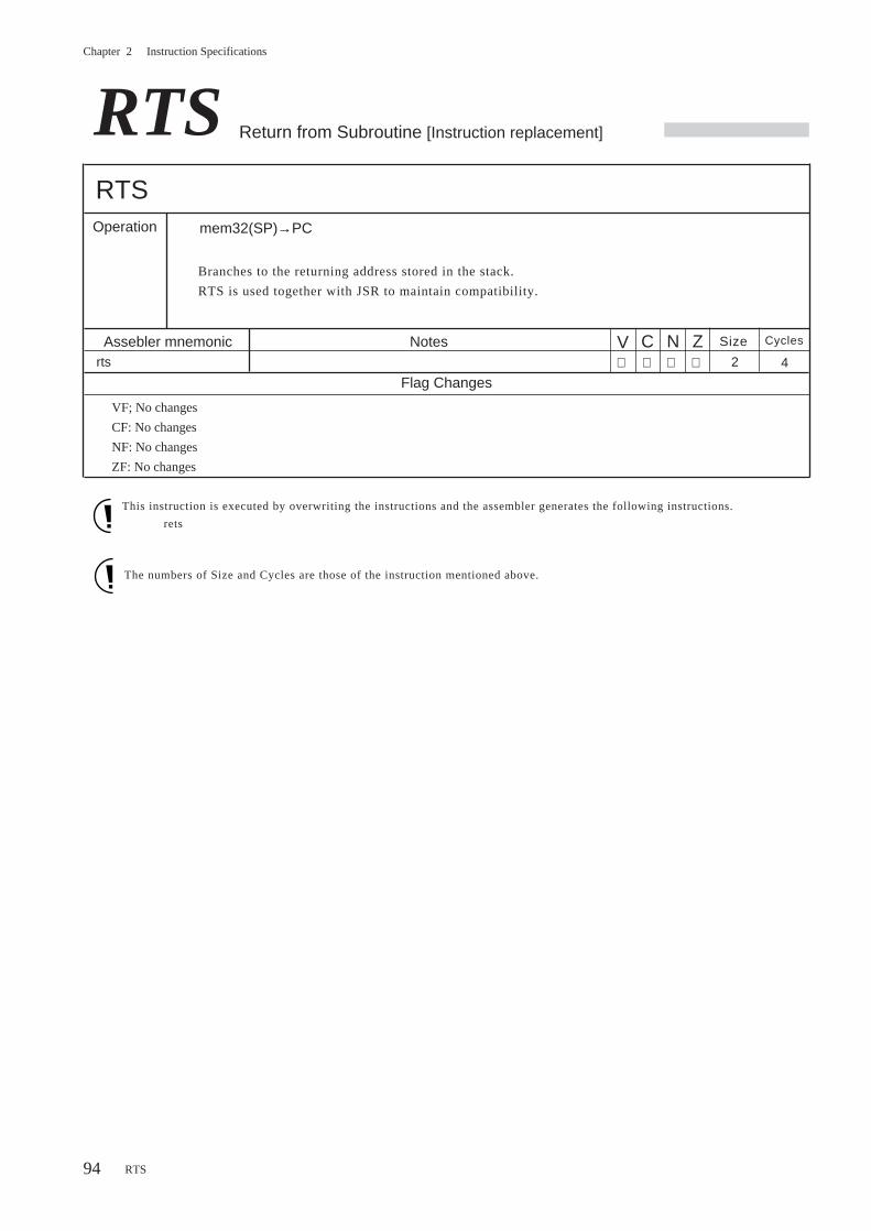
Chapter 2 Instruction Specifications
94
RTS Return from Subroutine [Instruction replacement]
RTS
V C Z
Operation
N
mem32(SP)→PC
Branches to the returning address stored in the stack.
RTS is used together with JSR to maintain compatibility.
Flag Changes
VF; No changes
CF: No changes
NF: No changes
ZF: No changes
Assebler mnemonic Size Cycles
rts
Notes2 4
RTS
This instruction is executed by overwriting the instructions and the assembler generates the following instructions.
rets
The numbers of Size and Cycles are those of the instruction mentioned above.
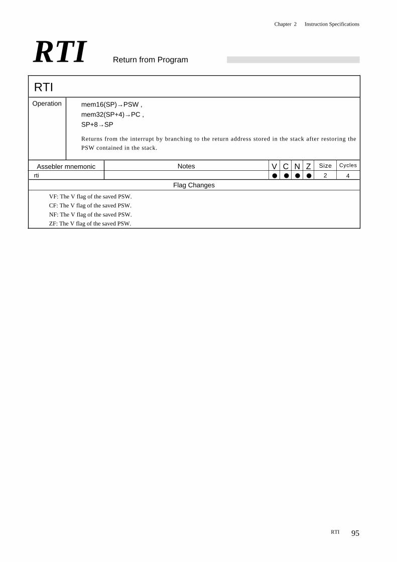
Chapter 2 Instruction Specifications
95
RTI Return from Program
RTIOperation
Returns from the interrupt by branching to the return address stored in the stack after restoring the
PSW contained in the stack.
mem16(SP)→PSW ,
mem32(SP+4)→PC ,
SP+8→SP
VF: The V flag of the saved PSW.
CF: The V flag of the saved PSW.
NF: The V flag of the saved PSW.
ZF: The V flag of the saved PSW.
Flag Changes
Assebler mnemonic Size Cycles
rti
Notes2 4
RTI
V C ZN● ● ● ●
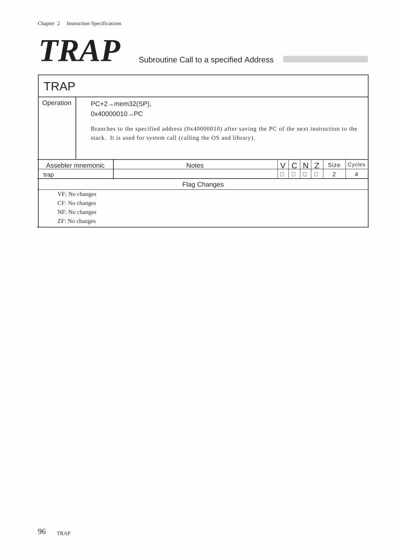
Chapter 2 Instruction Specifications
96
TRAP Subroutine Call to a specified Address
TRAP
V C Z
Operation
N
Branches to the specified address (0x40000010) after saving the PC of the next instruction to the
stack. It is used for system call (calling the OS and library).
PC+2→mem32(SP),
0x40000010→PC
Flag ChangesVF; No changes
CF: No changes
NF: No changes
ZF: No changes
Assebler mnemonic Size Cycles
trap
Notes2 4
TRAP
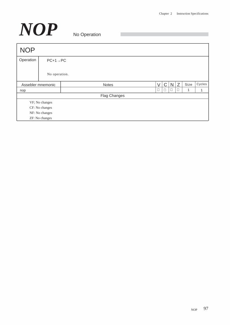
Chapter 2 Instruction Specifications
97
NOP No Operation
NOPOperation
No operation.
Flag Changes
VF; No changes
CF: No changes
NF: No changes
ZF: No changes
Assebler mnemonic Size Cycles
nop
Notes1 1
NOP
PC+1→PC
V C ZN
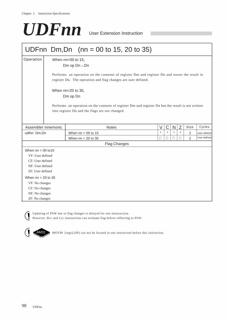
Chapter 2 Instruction Specifications
98
UDFnn User Extension Instruction
UDFnn Dm,Dn (nn = 00 to 15, 20 to 35)
V C Z
Operation
Performs an operation on the contents of register Dm and register Dn and stores the result in
register Dn. The operation and flag changes are user defined.
Performs an operation on the contents of register Dm and register Dn but the result is not written
into register Dn and the flags are not changed.
N
When nn=00 to 15,
Dm op Dn→Dn
Assembler mnemonic Size Cycles
udfnn Dm,Dn When nn = 00 to 15
When nn = 20 to 35
Notes
2
2
User defined
User defined
Flag Changes
When nn = 00 to15
VF: User defined
CF: User defined
NF: User defined
ZF: User defined
Updating of PSW due to flag changes is delayed for one insturuction.
However, Bcc and Lcc instructions can evaluate flag before reflecting to PSW.
When nn=20 to 35,
Dm op Dn
UDFnn
When nn = 20 to 35
VF: No changes
CF: No changes
NF: No changes
ZF: No changes
*
*
*
*
MOVM [regs],(SP) can not be located in one instruction before this instruction.AM31
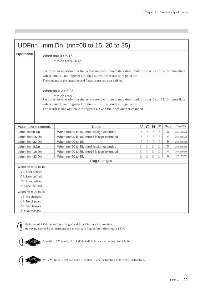
Chapter 2 Instruction Specifications
99
UDFnn imm,Dn (nn=00 to 15, 20 to 35)Operation
Performs an operation on the zero-extended immediate value(imm8 or imm16) or 32-bit immediate
value(imm32) and register Dn, then stores the result in register Dn.
The contents of the operation and flag changes are user defined.
Performs an operation on the zero-extended immediate value(imm8 or imm16) or 32-bit immediate
value(imm32) and register Dn, then stores the result in register Dn.
The result is not written into register Dn and the flags are not changed.
When nn= 00 to 15,
imm op Reg→Reg
UDFnn
When nn = 20 to 35,
imm op Reg
V C ZNAssembler mnemonic Size CyclesNotes
Flag Changes
udfnn imm8,Dn When nn=00 to 15, imm8 is sign-extended
udfnn imm16,Dn When nn=00 to 15, imm16 is sign-extended
udfnn imm32,Dn When nn=00 to 15,
udfnn imm8,Dn When nn=20 to 35, imm8 is sign-extended
udfnn imm16,Dn When nn=20 to 35, imm16 is sign-extended
udfnn imm32,Dn When nn=20 to 35,
3
4
6
User defined
User defined
User defined
User defined
User defined
User defined
*
*
*
*
*
*
*
*
*
*
*
*
3
4
6
When nn = 00 to 15
VF: User defined
CF: User defined
NF: User defined
ZF: User defined
When nn = 20 to 35
VF: No changes
CF: No changes
NF: No changes
ZF: No changes
Updating of PSW due to flag changes is delayed for one insturuction.
However, Bcc and Lcc instructions can evaluate flag before reflecting to PSW.
"nn=20 to 35" is only for AM31/AM32. It can not be used for AM30.AM30
MOVM [regs],(SP) can not be located in one instruction before this instruction.AM31
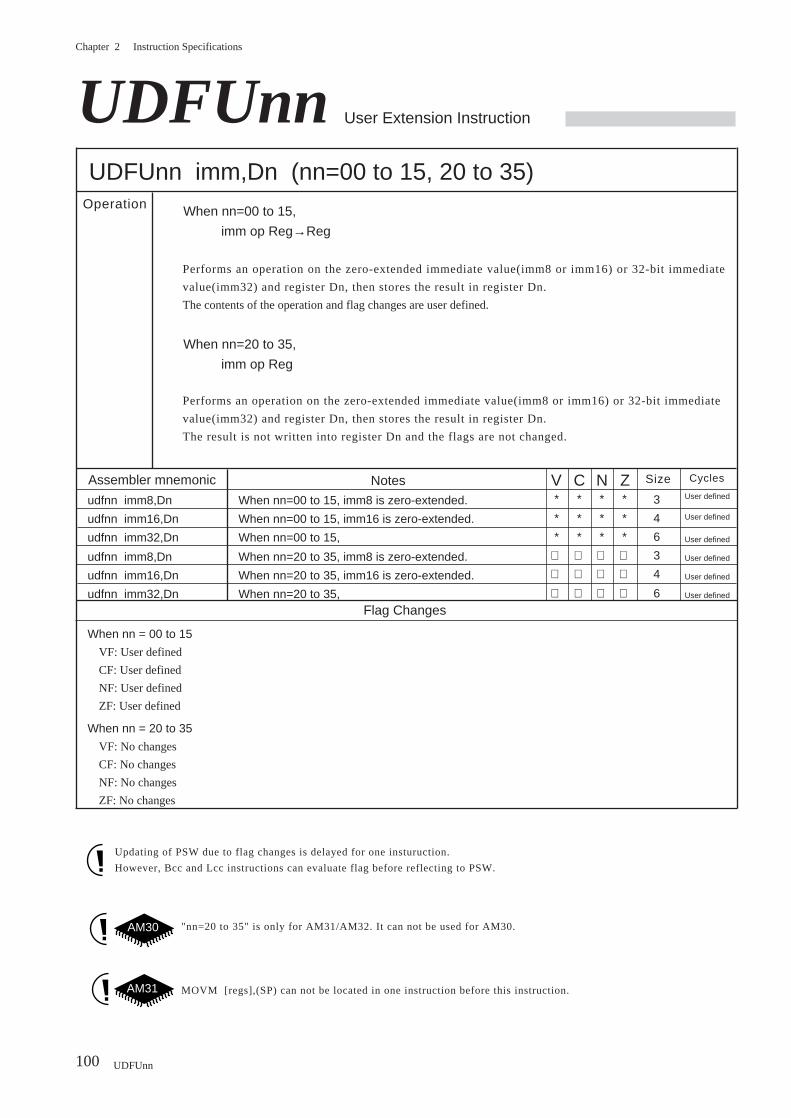
Chapter 2 Instruction Specifications
100
UDFUnn User Extension Instruction
UDFUnn
UDFUnn imm,Dn (nn=00 to 15, 20 to 35)Operation
Performs an operation on the zero-extended immediate value(imm8 or imm16) or 32-bit immediate
value(imm32) and register Dn, then stores the result in register Dn.
The contents of the operation and flag changes are user defined.
When nn=00 to 15,
imm op Reg→Reg
When nn=20 to 35,
imm op Reg
Performs an operation on the zero-extended immediate value(imm8 or imm16) or 32-bit immediate
value(imm32) and register Dn, then stores the result in register Dn.
The result is not written into register Dn and the flags are not changed.
V C ZNAssembler mnemonic Size CyclesNotes
Flag Changes
udfnn imm8,Dn When nn=00 to 15, imm8 is zero-extended.
udfnn imm16,Dn When nn=00 to 15, imm16 is zero-extended.
udfnn imm32,Dn When nn=00 to 15,
udfnn imm8,Dn When nn=20 to 35, imm8 is zero-extended.
udfnn imm16,Dn When nn=20 to 35, imm16 is zero-extended.
udfnn imm32,Dn When nn=20 to 35,
3
4
6
3
4
6
User defined
User defined
User defined
User defined
User defined
User defined
*
*
*
*
*
*
*
*
*
*
*
*
When nn = 00 to 15
VF: User defined
CF: User defined
NF: User defined
ZF: User defined
When nn = 20 to 35
VF: No changes
CF: No changes
NF: No changes
ZF: No changes
Updating of PSW due to flag changes is delayed for one insturuction.
However, Bcc and Lcc instructions can evaluate flag before reflecting to PSW.
"nn=20 to 35" is only for AM31/AM32. It can not be used for AM30.AM30
MOVM [regs],(SP) can not be located in one instruction before this instruction.AM31

3Usage Notes
Chapter 3 Usage Notes
102
Notes to Programmers
The MN1030/MN103S Series of 32-bit microcontrollers incorporates the following enhancements for boosting
throughput.
• Lower cycle counts
Additional hardware bypasses and augments the five-stage pipeline to increase the execution speeds of such
instructions as Lcc, SETLB, RET, and RETF.
• Higher operating frequencies
Reorganizing the pipeline stages to eliminate the bottlenecks associated with such operations as aligning
and expanding load data has permitted the use of shorter clock cycles.
To help your programs to take maximum advantage of these throughput enhancements, this Chapter describes
the pipeline architecture, dangerous code sequences, code sequences to avoid, and boiler plate code sequences.
1. Pipeline Architecture
This Section covers the structure and operation of the five-stage pipeline incorporated into the MN1030/
MN103S Series of 32-bit microcontrollers.
2. Dangerous Code Sequences
This Section describes instruction variants and instruction sequences that must be strictly avoided
because they lead to faulty operation.
3. Code Sequences to Avoid
This Section describes instruction variants and instruction sequences that should be avoided not
because they lead to faulty operation, but because they consume excess cycles.
4. Boiler Plate Code Sequences
This Section contains sample code for common programming tasks.
Pipeline Architecture
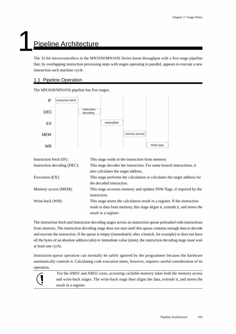
Chapter 3 Usage Notes
103
Pipeline Architecture
The 32-bit microcontrollers in the MN1030/MN103S Series boost throughput with a five-stage pipeline
that, by overlapping instruction processing steps with stages operating in parallel, appears to execute a new
instruction each machine cycle.
1.1 Pipeline Operation
The MN1030/MN103S pipeline has five stages.
Instruction fetch (IF): This stage reads in the instruction from memory
Instruction decoding (DEC): This stage decodes the instruction. For some branch instructions, it
also calculates the target address.
Execution (EX): This stage performs the calculation or calculates the target address for
the decoded instruction.
Memory access (MEM): This stage accesses memory and updates PSW flags, if required by the
instruction.
Write-back (WB): This stage stores the calculation result in a register. If the instruction
reads in data from memory, this stage aligns it, extends it, and stores the
result in a register.
The instruction fetch and instruction decoding stages access an instruction queue preloaded with instructions
from memory. The instruction decoding stage does not start until this queue contains enough data to decode
and execute the instruction. If the queue is empty (immediately after a branch, for example) or does not have
all the bytes of an absolute address (abs) or immediate value (imm), the instruction decoding stage must wait
at least one cycle.
Instruction queue operation can normally be safely ignored by the programmer because the hardware
automatically controls it. Calculating code execution times, however, requires careful consideration of its
operation.
For the AM31 and AM32 cores, accessing cachable memory takes both the memory access
and write-back stages. The write-back stage then aligns the data, extends it, and stores the
result in a register.
1
Pipeline Architecture
instruction �decoding
memory access
execution
Write back
DEC
MEM
EX
WB
instruction fetchIF
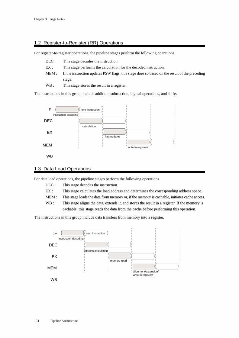
Chapter 3 Usage Notes
104
1.2 Register-to-Register (RR) Operations
For register-to-register operations, the pipeline stages perform the following operations.
DEC : This stage decodes the instruction.
EX : This stage performs the calculation for the decoded instruction.
MEM : If the instruction updates PSW flags, this stage does so based on the result of the preceding
stage.
WB : This stage stores the result in a register.
The instructions in this group include addition, subtraction, logical operations, and shifts.
1.3 Data Load Operations
For data load operations, the pipeline stages perform the following operations.
DEC : This stage decodes the instruction.
EX : This stage calculates the load address and determines the corresponding address space.
MEM : This stage loads the data from memory or, if the memory is cachable, initiates cache access.
WB : This stage aligns the data, extends it, and stores the result in a register. If the memory is
cachable, this stage reads the data from the cache before performing this operation.
The instructions in this group include data transfers from memory into a register.
Pipeline Architecture
calculation
write in registers
flag updates
DEC
IF
MEM
EX
WB
instruction decoding
next instruction
address calculation
alignment/extension/write in registers
memory read
DEC
MEM
EX
WB
instruction decoding
IF next instruction
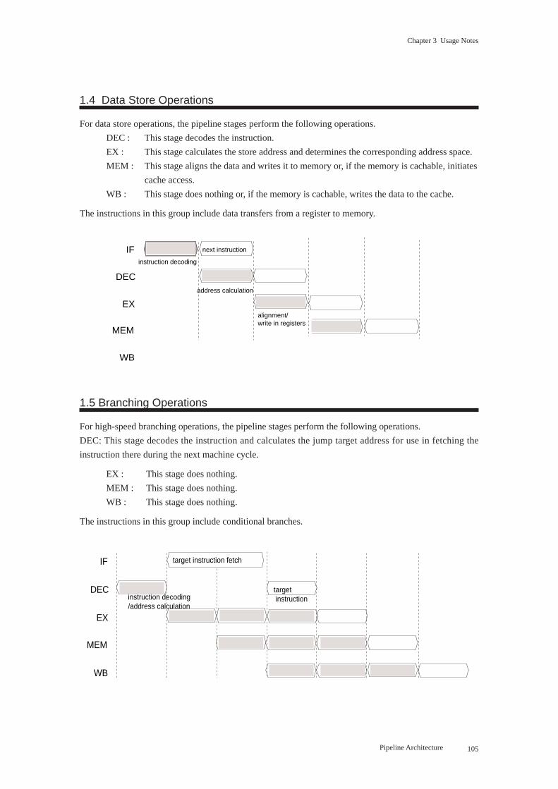
Chapter 3 Usage Notes
105
1.4 Data Store Operations
For data store operations, the pipeline stages perform the following operations.
DEC : This stage decodes the instruction.
EX : This stage calculates the store address and determines the corresponding address space.
MEM : This stage aligns the data and writes it to memory or, if the memory is cachable, initiates
cache access.
WB : This stage does nothing or, if the memory is cachable, writes the data to the cache.
The instructions in this group include data transfers from a register to memory.
1.5 Branching Operations
For high-speed branching operations, the pipeline stages perform the following operations.
DEC: This stage decodes the instruction and calculates the jump target address for use in fetching the
instruction there during the next machine cycle.
EX : This stage does nothing.
MEM : This stage does nothing.
WB : This stage does nothing.
The instructions in this group include conditional branches.
address calculation
alignment/write in registers
DEC
MEM
EX
WB
instruction decoding
IF next instruction
instruction decoding/address calculation
target instruction
target instruction fetch
DEC
MEM
EX
WB
IF
Pipeline Architecture
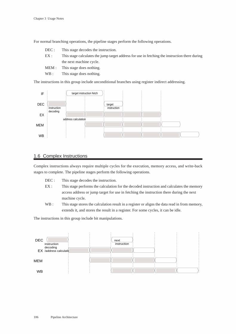
Chapter 3 Usage Notes
106
For normal branching operations, the pipeline stages perform the following operations.
DEC : This stage decodes the instruction.
EX : This stage calculates the jump target address for use in fetching the instruction there during
the next machine cycle.
MEM : This stage does nothing.
WB : This stage does nothing.
The instructions in this group include unconditional branches using register indirect addressing.
1.6 Complex Instructions
Complex instructions always require multiple cycles for the execution, memory access, and write-back
stages to complete. The pipeline stages perform the following operations.
DEC : This stage decodes the instruction.
EX : This stage performs the calculation for the decoded instruction and calculates the memory
access address or jump target for use in fetching the instruction there during the next
machine cycle.
WB : This stage stores the calculation result in a register or aligns the data read in from memory,
extends it, and stores the result in a register. For some cycles, it can be idle.
The instructions in this group include bit manipulations.
Pipeline Architecture
target instruction
target instruction fetch
instruction decoding
DEC
MEM
EX
WB
IF
address calculation
instruction decoding/address calculation
next instruction
DEC
MEM
EX
WB
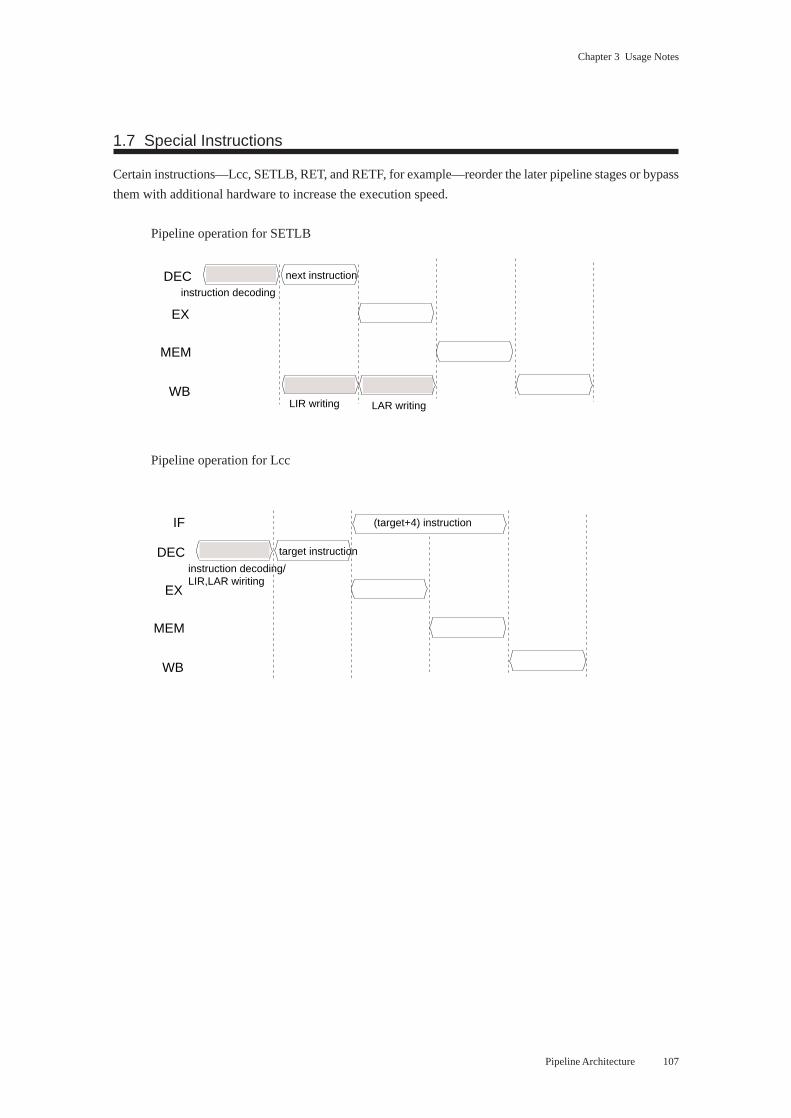
Chapter 3 Usage Notes
107
1.7 Special Instructions
Certain instructions—Lcc, SETLB, RET, and RETF, for example—reorder the later pipeline stages or bypass
them with additional hardware to increase the execution speed.
Pipeline operation for SETLB
Pipeline operation for Lcc
Pipeline Architecture
LIR writing LAR writing
DEC
MEM
EX
WB
instruction decoding
next instruction
(target+4) instruction
DEC
MEM
EX
WB
instruction decoding/LIR,LAR wiriting
target instruction
IF
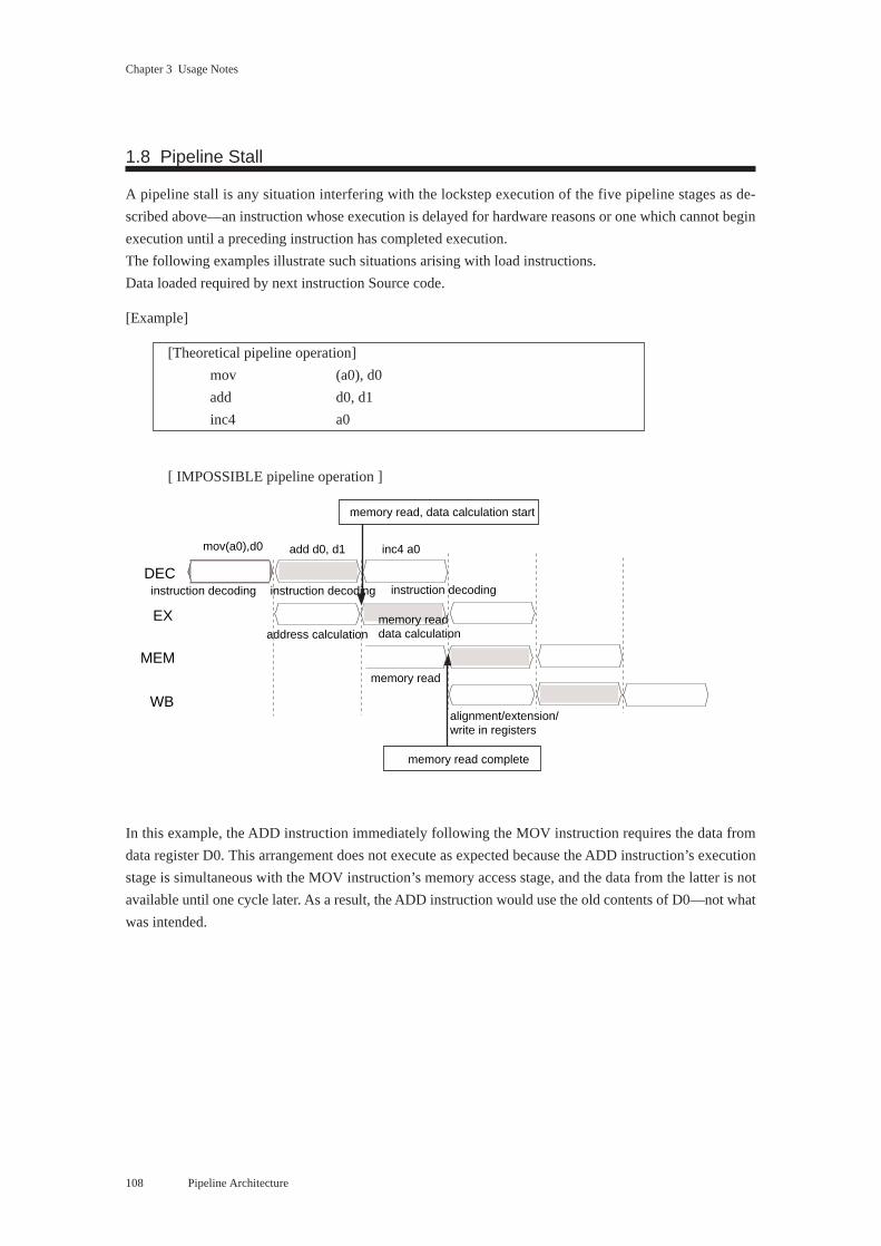
Chapter 3 Usage Notes
108
1.8 Pipeline Stall
A pipeline stall is any situation interfering with the lockstep execution of the five pipeline stages as de-
scribed above—an instruction whose execution is delayed for hardware reasons or one which cannot begin
execution until a preceding instruction has completed execution.
The following examples illustrate such situations arising with load instructions.
Data loaded required by next instruction Source code.
[Example]
[Theoretical pipeline operation]
mov (a0), d0
add d0, d1
inc4 a0
[ IMPOSSIBLE pipeline operation ]
In this example, the ADD instruction immediately following the MOV instruction requires the data from
data register D0. This arrangement does not execute as expected because the ADD instruction’s execution
stage is simultaneous with the MOV instruction’s memory access stage, and the data from the latter is not
available until one cycle later. As a result, the ADD instruction would use the old contents of D0—not what
was intended.
Pipeline Architecture
alignment/extension/write in registers
memory read
DEC
MEM
EX
WB
instruction decoding
mov(a0),d0
instruction decoding instruction decoding
add d0, d1 inc4 a0
address calculationmemory readdata calculation
memory read complete
memory read, data calculation start
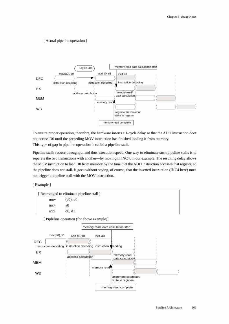
Chapter 3 Usage Notes
109
[ Actual pipeline operation ]
To ensure proper operation, therefore, the hardware inserts a 1-cycle delay so that the ADD instruction does
not access D0 until the preceding MOV instruction has finished loading it from memory.
This type of gap in pipeline operation is called a pipeline stall.
Pipeline stalls reduce throughput and thus execution speed. One way to eliminate such pipeline stalls is to
separate the two instructions with another—by moving in INC4, in our example. The resulting delay allows
the MOV instruction to load D0 from memory by the time that the ADD instruction accesses that register, so
the pipeline does not stall. It goes without saying, of course, that the inserted instruction (INC4 here) must
not trigger a pipeline stall with the MOV instruction.
[ Example ]
[ Rearranged to eliminate pipeline stall ]
mov (a0), d0
inc4 a0
add d0, d1
[ Pipleline operation (for above example)]
Pipeline Architecture
memory read
alignment/extension/write in register
DEC
MEM
EX
WB
instruction decoding
address calculation
1cycle late
memory read/data calculation
instruction decoding instruction decoding
memory read data calculation start
inc4 a0add d0, d1mov(a0), d0
memory read complete
alignment/extension/write in registers
memory read
DEC
MEM
EX
WB
instruction decoding
mov(a0),d0
instruction decoding instruction decoding
add d0, d1 inc4 a0
address calculationmemory readdata calculation
memory read complete
memory read, data calculation start
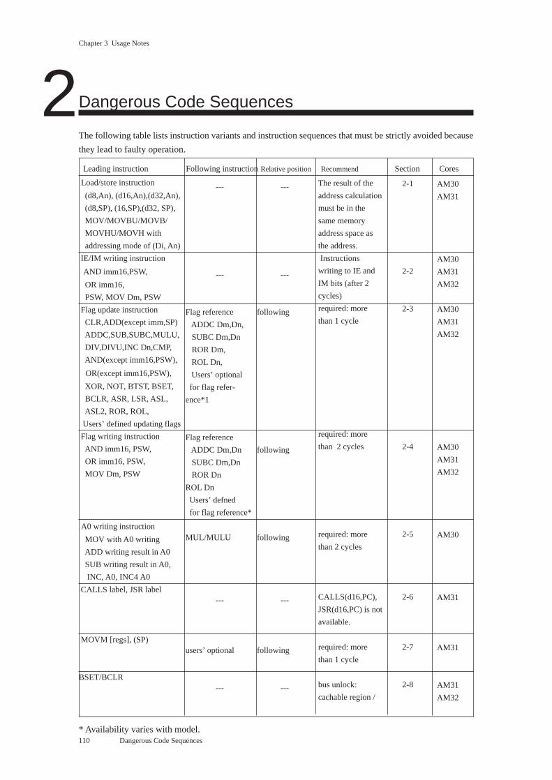
Chapter 3 Usage Notes
110
Dangerous Code Sequences
The following table lists instruction variants and instruction sequences that must be strictly avoided because
they lead to faulty operation.
Leading instruction Following instructionRelative position Recommend Section Cores
Load/store instruction
(d8,An), (d16,An),(d32,An),
(d8,SP), (16,SP),(d32, SP),
MOV/MOVBU/MOVB/
MOVHU/MOVH with
addressing mode of (Di, An)
IE/IM writing instruction
AND imm16,PSW,
OR imm16,
PSW, MOV Dm, PSW
Flag update instruction
CLR,ADD(except imm,SP)
ADDC,SUB,SUBC,MULU,
DIV,DIVU,INC Dn,CMP,
AND(except imm16,PSW),
OR(except imm16,PSW),
XOR, NOT, BTST, BSET,
BCLR, ASR, LSR, ASL,
ASL2, ROR, ROL,
Users’ defined updating flags
Flag writing instruction
AND imm16, PSW,
OR imm16, PSW,
MOV Dm, PSW
A0 writing instruction
MOV with A0 writing
ADD writing result in A0
SUB writing result in A0,
INC, A0, INC4 A0
CALLS label, JSR label
MOVM [regs], (SP)
BSET/BCLR
* Availability varies with model.Dangerous Code Sequences
---
---
Flag reference
ADDC Dm,Dn,
SUBC Dm,Dn
ROR Dm,
ROL Dn,
Users’ optional
for flag refer-
ence*1
Flag reference
ADDC Dm,Dn
SUBC Dm,Dn
ROR Dn
ROL Dn
Users’ defned
for flag reference*
MUL/MULU
---
users’ optional
---
---
---
following
following
following
---
following
---
The result of the
address calculation
must be in the
same memory
address space as
the address.
Instructions
writing to IE and
IM bits (after 2
cycles)
required: more
than 1 cycle
required: more
than 2 cycles
required: more
than 2 cycles
CALLS(d16,PC),
JSR(d16,PC) is not
available.
required: more
than 1 cycle
bus unlock:
cachable region /
2-1
2-2
2-3
2-4
2-5
2-6
2-7
2-8
AM30
AM31
AM30
AM31
AM32
AM30
AM31
AM32
AM30
AM31
AM32
AM30
AM31
AM31
AM31
AM32
2
Chapter 3 Usage Notes
111
The descriptions in this section have the following components.
[ Description ]
These portions describe the problems and include pipeline operation diagrams.
[ Icons ]
Warning: This icon indicates warnings that must always be observed.
These indicate the applicable microcontroller cores.
[ Example ]
These portions illustrate the problems with specific coding examples—both problematic versions that do
not execute as expected and revised versions guaranteed to execute properly.
[ Applicable Instructions ]
These portions list the instruction variants and instruction sequences exhibiting the problem.
The coding examples labeled “problematic” below do not necessarily always fail to yield the
expected results. If two instructions, A and B, must always be separated by at least one cycle,
they will still execute as expected together if memory location, interrupts, and other factors
conspire to delay the supply of instruction B to the pipeline. For “worst case” reliability,
however, always use the revised version instead.
For ease of clarification, the coding examples below use NOPs to separate instructions, but
these are not the only candidates. Any instruction in the vicinity that can be moved into the
gap without changing program logic or presenting ordering problems of its own makes a
better candidate.
Dangerous Code Sequences
AM32AM31AM30
Chapter 3 Usage Notes
112
2.1 Load/Store Instructions
[ Description ]
To speed memory access, load/store instructions assume that the memory space accessed is that of the base
address, so determine it from that in an operation that runs parallel to the address calculation. If the result is
in a different memory space, however, faulty operation results. To avoid this problem, always make sure that
the base address and the result are in the same memory space.
[ Example ]
Problematic Version
mov 0x20, a0
mov (0x80000000,a0), d0
base address address calculation result
a0=0x00000020 a0+0x8000000
=0x8000020
ROM/RAM/Flash memory internal data RAM space external memory space
with Cache cachable region for data uncachable region
different
This code does not execute as expected because the base address and the result are in different memory spaces.
Revised Version
mov 0x80000000, a0
mov (0x20, a0), d0
base address address calculation result
a0=0x00000020 a0+0x8000000
=0x8000020
ROM/RAM/Flash memory internal data RAM space external memory space
with Cache cachable region for data uncachable region
same
This code executes without problem because the base address and the result are in the same memory space.
[ Applicable Instructions ]
MOV, MOVBU, MOVB, MOVHU, and MOVH with the following addressing modes
Addressing Modes Base Address
(d8,An)/(d16,An)/(d32,An) An
(d8,SP)/(d16,SP)/(d32,SP) SP
(Di,An) An
AM30
AM31
Notes
calculation
memory access
DEC
MEM
EX
WB
instruction decoding
accessing space starts
address determinedfor accessed space
Dangerous Code Sequences
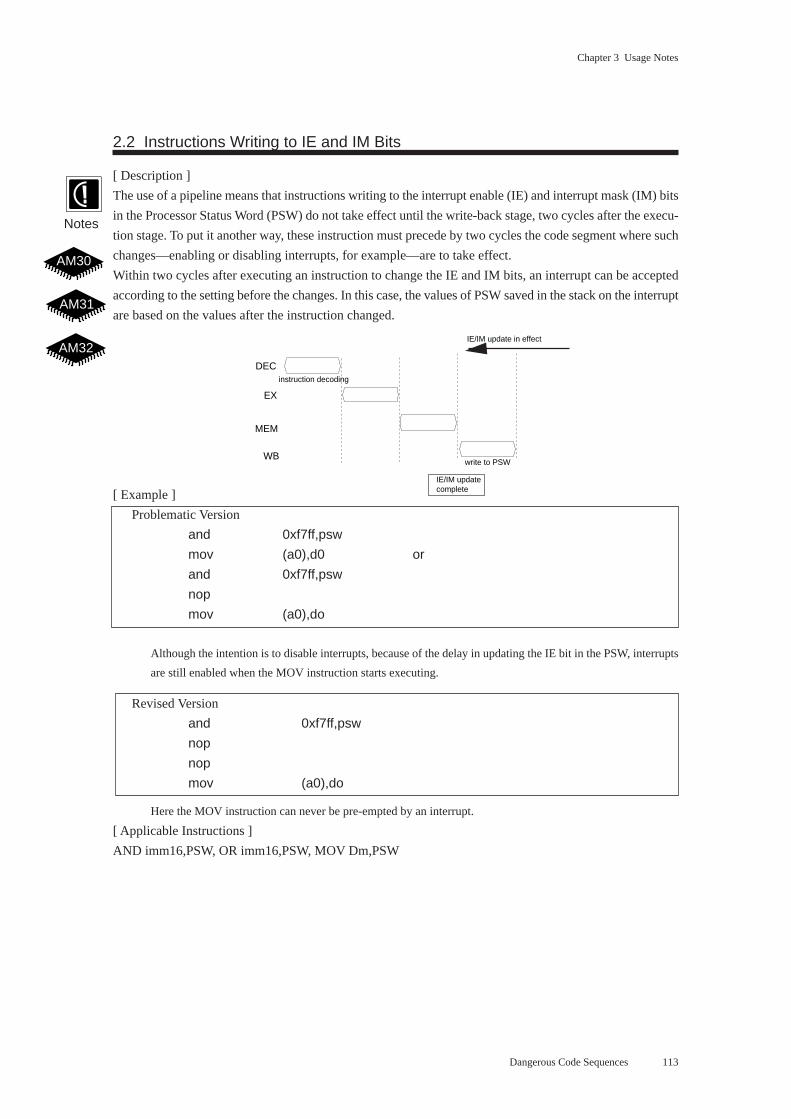
Chapter 3 Usage Notes
113
2.2 Instructions Writing to IE and IM Bits
[ Description ]
The use of a pipeline means that instructions writing to the interrupt enable (IE) and interrupt mask (IM) bits
in the Processor Status Word (PSW) do not take effect until the write-back stage, two cycles after the execu-
tion stage. To put it another way, these instruction must precede by two cycles the code segment where such
changes—enabling or disabling interrupts, for example—are to take effect.
Within two cycles after executing an instruction to change the IE and IM bits, an interrupt can be accepted
according to the setting before the changes. In this case, the values of PSW saved in the stack on the interrupt
are based on the values after the instruction changed.
[ Example ]
Problematic Version
and 0xf7ff,psw
mov (a0),d0 or
and 0xf7ff,psw
nop
mov (a0),do
Although the intention is to disable interrupts, because of the delay in updating the IE bit in the PSW, interrupts
are still enabled when the MOV instruction starts executing.
Revised Version
and 0xf7ff,psw
nop
nop
mov (a0),do
Here the MOV instruction can never be pre-empted by an interrupt.
[ Applicable Instructions ]
AND imm16,PSW, OR imm16,PSW, MOV Dm,PSW
Dangerous Code Sequences
AM32
AM31
AM30
Notes
write to PSW
DEC
MEM
EX
WB
instruction decoding
IE/IM update in effect
IE/IM update complete
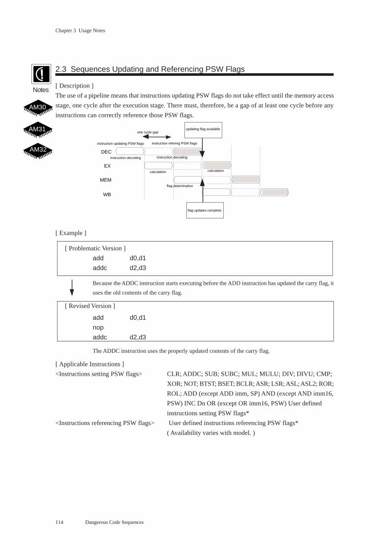
Chapter 3 Usage Notes
114
2.3 Sequences Updating and Referencing PSW Flags
[ Description ]
The use of a pipeline means that instructions updating PSW flags do not take effect until the memory access
stage, one cycle after the execution stage. There must, therefore, be a gap of at least one cycle before any
instructions can correctly reference those PSW flags.
[ Example ]
[ Problematic Version ]
add d0,d1
addc d2,d3
Because the ADDC instruction starts executing before the ADD instruction has updated the carry flag, it
uses the old contents of the carry flag.
[ Revised Version ]
add d0,d1
nop
addc d2,d3
The ADDC instruction uses the properly updated contents of the carry flag.
[ Applicable Instructions ]
<Instructions setting PSW flags> CLR; ADDC; SUB; SUBC; MUL; MULU; DIV; DIVU; CMP;
XOR; NOT; BTST; BSET; BCLR; ASR; LSR; ASL; ASL2; ROR;
ROL; ADD (except ADD imm, SP) AND (except AND imm16,
PSW) INC Dn OR (except OR imm16, PSW) User defined
instructions setting PSW flags*
<Instructions referencing PSW flags> User defined instructions referencing PSW flags*
( Availability varies with model. )
Dangerous Code Sequences
flag detemination
DEC
MEM
EX
WB
instruction decoding
instruction updating PSW flags
instruction decoding
instruction refering PSW flags
calculation calculation
flag updates complete
updating flag availableone cycle gap
Notes
AM30
AM31
AM32
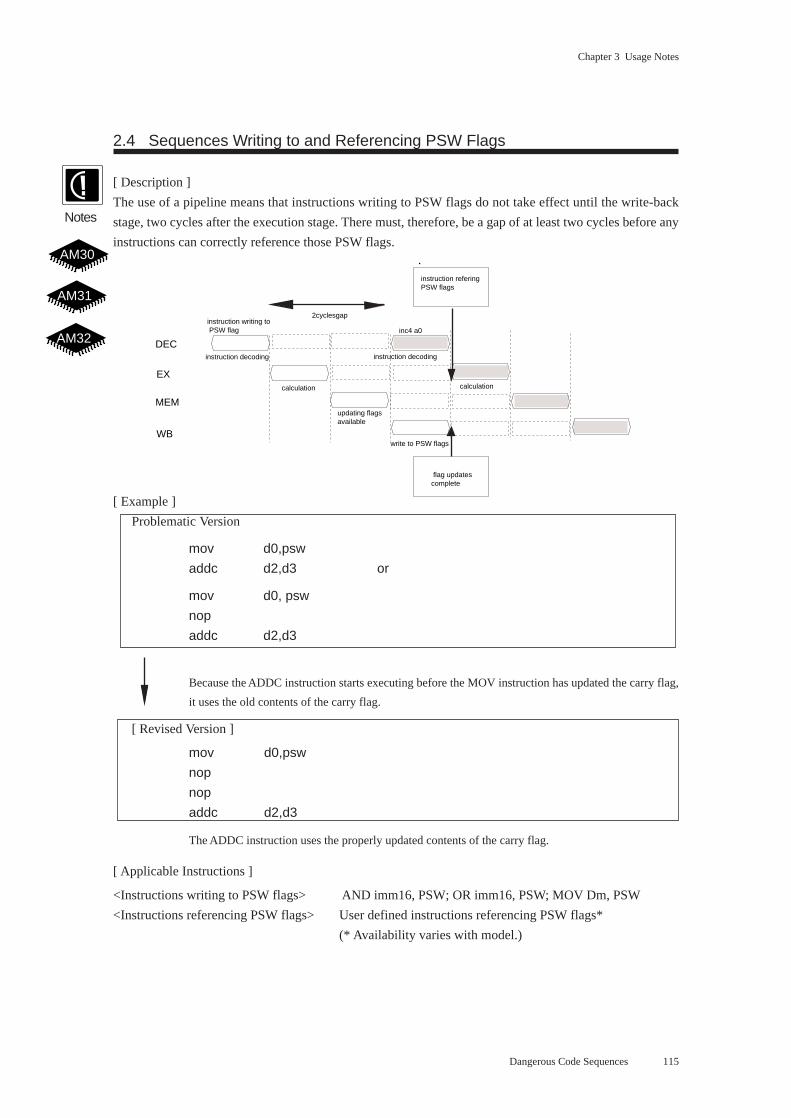
Chapter 3 Usage Notes
115
2.4 Sequences Writing to and Referencing PSW Flags
[ Description ]
The use of a pipeline means that instructions writing to PSW flags do not take effect until the write-back
stage, two cycles after the execution stage. There must, therefore, be a gap of at least two cycles before any
instructions can correctly reference those PSW flags.
[ Example ]
Problematic Version
mov d0,psw
addc d2,d3 or
mov d0, psw
nop
addc d2,d3
Because the ADDC instruction starts executing before the MOV instruction has updated the carry flag,
it uses the old contents of the carry flag.
[ Revised Version ]
mov d0,psw
nop
nop
addc d2,d3
The ADDC instruction uses the properly updated contents of the carry flag.
[ Applicable Instructions ]
<Instructions writing to PSW flags> AND imm16, PSW; OR imm16, PSW; MOV Dm, PSW
<Instructions referencing PSW flags> User defined instructions referencing PSW flags*
(* Availability varies with model.)
Dangerous Code Sequences
Notes
AM30
AM32
AM31
updating flags available
write to PSW flags
DEC
MEM
EX
WB
instruction decoding
calculation
2cyclesgap
instruction decoding
inc4 a0instruction writing to PSW flag
calculation
instruction refering PSW flags
flag updates complete
Chapter 3 Usage Notes
116
2.5 MUL/MULU after Write to A0
[ Description ]
To boost execution speed, the AM30 versions of the MUL and MULU instructions modify pipeline opera-
tion in a way that interacts with the address register A0. As a result, there must be a gap of at least two cycles
after any instruction that writes to A0 before these two instructions. Example
[Example ]
[ Problematic Version ]
mov 0x12345678,a0
mul d0,d1 or
mov 0x12345678,a0
nop
mul d0,d1Assembling the source file (program.asm) containing the above code with the -mno-nopmul command
line option produces object code reflecting the source code exactly as written—
as103 -mno-popmul program.asm
that is, no additional NOPs. This object code, however, does not always perform as intended.
[ Revised Version ]
mov 0x12345678,a0
nop
nop
mul d0,d1
Inserting the necessary NOPs or assembling the source file with the -mnopmul command line option
produces object code with the necessary two-cycle gap and thus guaranteed to execute properly.
as103 -mnopmul program.asm
specifying these options is to insert two NOPs between Instruction writing to Ao and MUL/
NULU and generate the object files.
The assembler defaults to the -mnopmul command line option.
[ Applicable Instructions ]
<Instruction writing to A0> all MOV, ADD, and SUB instructions writing to A0; INC A0; INC4 A0
Dangerous Code Sequences
Notes
AM30
Chapter 3 Usage Notes
117
2.6 Displacements with CALLS and JSR (AM31 Only)
[ Description ]
To boost execution speed, the AM31 versions of the CALLS and JSR instructions modify pipeline operation
in a way that prevents the use of 16-bit displacements. The CALLS (d16, PC) and JSR (d16, PC) variants are
not available, so use the d32 variants instead.
The command line option for disabling the use of such 16-bit displacements is -mlongcalls.
[ Example ]
Assembling the source file (program.asm) containing the above code with the -mlongcalls command
line option produces object code reflecting the source code exactly as written—
as103 -mlongcalls program.asm
specifying these option is to generate the object files as CALL(d32,PC) or JSR(d32,PC) without using
CALLS(d16,PC) ir JSR(d16,PC)
[ Applicable Instructions ]
CALLS (d16,PC), JSR (d16,PC)
Dangerous Code Sequences
AM31
Notes
Chapter 3 Usage Notes
118
2.7 User Defined Instructions after MOVM [regs], (SP) (AM31 Only)
[ Description ]
To boost execution speed, the AM31 version of MOVM [regs], (SP) modifies pipeline operation in a way
that introduces a structural dependency with immediately following user defined instructions (UDFnn and
UDFUnn). As a result, there must be a gap of at least one cycle between the two.
[ Example ]
[ Problematic Version ]
movm [regs], (SP)
udf00 d0, d1
Assembling the source file (program.asm) containing the above code with the -mno-nopmovm com-
mand line option produces object code reflecting the source code exactly as written—
as103 -mno-nopmovm program.asm
that is, no intervening NOP. This object code, however, does not always perform as intended.
[ Revised Version ]
movm [regs], (SP)
nop
udf00 d0, d1
Inserting the necessary NOP or assembling the source file with the -mnopmovm command line option
produces object code with the necessary one-cycle gap and thus guaranteed to execute properly.
as103 -mnopmovm program.asm
Specifying these options is to insert one NOP between MOVM[regs],(SP) and UDFnn/UDFUnn and
generates the object files.
The assembler defaults to the -mnopmovm command line option.
[ Applicable Instructions ]
<Leading instruction> MOVM[regs], (SP)
<User defined instructions> (UDFnn and UDFUnn)*
(* Availability varies with model. )
AM31
Notes
Dangerous Code Sequences
Chapter 3 Usage Notes
119
2.8 BSET and BCLR with Cachable External Memory
[ Description ]
The bit manipulation instructions BSET and BCLR, because of their importance to semaphore management,
normally lock the bus for exclusive CPU use while they execute. The AM31 and AM32 versions, however,
do not lock the bus for operations on data in the cachable region of external memory because the operations
bypass the bus, accessing the cache, not the memory itself.
[ Applicable Instructions ]
BSET, BCLR
AM31
Notes
Dangerous Code Sequences
AM32
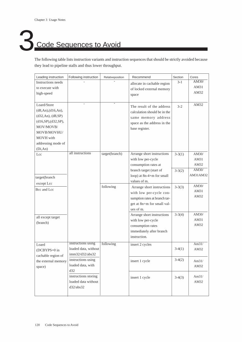
120
Chapter 3 Usage Notes
Code Sequences to Avoid
The following table lists instruction variants and instruction sequences that should be strictly avoided because
they lead to pipeline stalls and thus lower throughput.
Leading instruction Following instruction Relativeposition Recommend Section Cores
Instructions needs
to execute with
high-speed
Loard/Store
(d8,An),(d16,An),
(d32,An), (d8,SP)
(d16,SP),(d32,SP),
MOV/MOVB/
MOVB/MOVHU/
MOVH with
addressing mode of
(Di,An)
Lcc
target(branch
except Lcc
Bcc and Lcc
all except target
(branch)
Loard
(DCBYPS=0 in
cachable region of
the external memory
space)
3-
-
all instructions
instructions using
loaded data, without
imm32/d32/abs32
instructions using
loaded data, with
d32
instructions storing
loaded data without
d32/abs32
-
-
target(branch)
following
following
allocate in cachable region
of locked external memory
space
The result of the address
calculation should be in the
same memory address
space as the address in the
base register.
Arrange short instructions
with low per-cycle
consumption rates at
branch target (start of
loop) at 8n-4+m for small
values of m.
Arrange short instructions
with low per-cycle con-
sumption rates at branch tar-
get at 8n+m for small val-
ues of m.
Arrange short instructions
with low per-cycle
consumption rates
immediately after branch
instruction.
insert 2 cycles
insert 1 cycle
insert 1 cycle
3-1
3-2
3-3(1)
3-3(2)
3-3(3)
3-3(4)
3-4(1)
3-4(2)
3-4(3)
AM30/
AM31
AM32
AM32
AM30/
AM31
AM32
AM30/
AM31AM32
AM30/
AM31
AM32
AM30/
AM31
AM32
Am31/
AM32
Am31/
AM32
Am31/
AM32
Code Sequences to Avoid
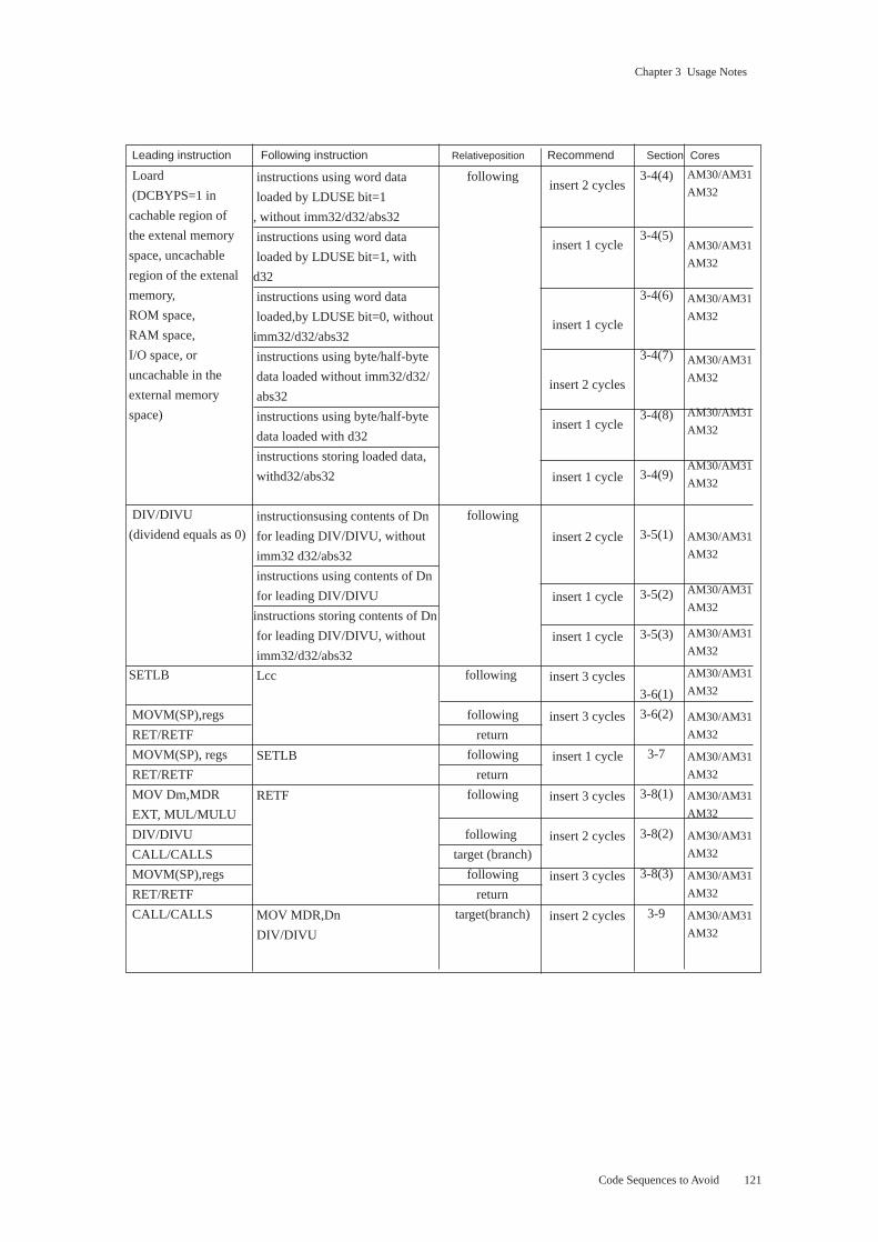
121
Chapter 3 Usage Notes
Leading instruction Following instruction Relativeposition Recommend Section Cores
Loard
(DCBYPS=1 in
cachable region of
the extenal memory
space, uncachable
region of the extenal
memory,
ROM space,
RAM space,
I/O space, or
uncachable in the
external memory
space)
DIV/DIVU
(dividend equals as 0)
SETLB
MOVM(SP),regs
RET/RETF
MOVM(SP), regs
RET/RETF
MOV Dm,MDR
EXT, MUL/MULU
DIV/DIVU
CALL/CALLS
MOVM(SP),regs
RET/RETF
CALL/CALLS
Code Sequences to Avoid
instructions using word data
loaded by LDUSE bit=1
, without imm32/d32/abs32
instructions using word data
loaded by LDUSE bit=1, with
d32
instructions using word data
loaded,by LDUSE bit=0, without
imm32/d32/abs32
instructions using byte/half-byte
data loaded without imm32/d32/
abs32
instructions using byte/half-byte
data loaded with d32
instructions storing loaded data,
withd32/abs32
instructionsusing contents of Dn
for leading DIV/DIVU, without
imm32 d32/abs32
instructions using contents of Dn
for leading DIV/DIVU
instructions storing contents of Dn
for leading DIV/DIVU, without
imm32/d32/abs32
Lcc
SETLB
RETF
MOV MDR,Dn
DIV/DIVU
following
following
following
following
return
following
return
following
following
target (branch)
following
return
target(branch)
insert 2 cycles
insert 1 cycle
insert 1 cycle
insert 2 cycles
insert 1 cycle
insert 1 cycle
insert 2 cycle
insert 1 cycle
insert 1 cycle
insert 3 cycles
insert 3 cycles
insert 1 cycle
insert 3 cycles
insert 2 cycles
insert 3 cycles
insert 2 cycles
3-4(4)
3-4(5)
3-4(6)
3-4(7)
3-4(8)
3-4(9)
3-5(1)
3-5(2)
3-5(3)
3-6(1)
3-6(2)
3-7
3-8(1)
3-8(2)
3-8(3)
3-9
AM30/AM31
AM32
AM30/AM31
AM32
AM30/AM31
AM32
AM30/AM31
AM32
AM30/AM31
AM32
AM30/AM31
AM32
AM30/AM31
AM32
AM30/AM31
AM32
AM30/AM31
AM32
AM30/AM31
AM32
AM30/AM31
AM32
AM30/AM31
AM32
AM30/AM31
AM32
AM30/AM31
AM32
AM30/AM31
AM32
AM30/AM31
AM32
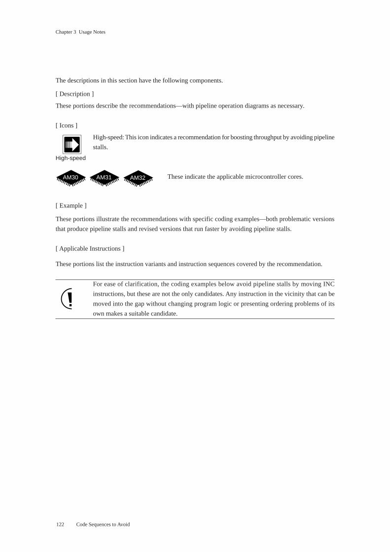
122
Chapter 3 Usage Notes
The descriptions in this section have the following components.
[ Description ]
These portions describe the recommendations—with pipeline operation diagrams as necessary.
[ Icons ]
High-speed: This icon indicates a recommendation for boosting throughput by avoiding pipeline
stalls.
These indicate the applicable microcontroller cores.
[ Example ]
These portions illustrate the recommendations with specific coding examples—both problematic versions
that produce pipeline stalls and revised versions that run faster by avoiding pipeline stalls.
[ Applicable Instructions ]
These portions list the instruction variants and instruction sequences covered by the recommendation.
For ease of clarification, the coding examples below avoid pipeline stalls by moving INC
instructions, but these are not the only candidates. Any instruction in the vicinity that can be
moved into the gap without changing program logic or presenting ordering problems of its
own makes a suitable candidate.
High-speed
AM31 AM32
Code Sequences to Avoid
AM30
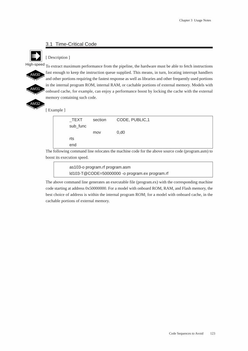
123
Chapter 3 Usage Notes
3.1 Time-Critical Code
[ Description ]
To extract maximum performance from the pipeline, the hardware must be able to fetch instructions
fast enough to keep the instruction queue supplied. This means, in turn, locating interrupt handlers
and other portions requiring the fastest response as well as libraries and other frequently used portions
in the internal program ROM, internal RAM, or cachable portions of external memory. Models with
onboard cache, for example, can enjoy a performance boost by locking the cache with the external
memory containing such code.
[ Example ]
_TEXT section CODE, PUBLIC,1
sub_func
mov 0,d0
rts
end
The following command line relocates the machine code for the above source code (program.asm) to
boost its execution speed.
as103-o program.rf program.asm
ld103-T@CODE=50000000 -o program.ex program.rf
The above command line generates an executable file (program.ex) with the corresponding machine
code starting at address 0x50000000. For a model with onboard ROM, RAM, and Flash memory, the
best choice of address is within the internal program ROM; for a model with onboard cache, in the
cachable portions of external memory.
AM30
Code Sequences to Avoid
High-speed
AM31
AM32
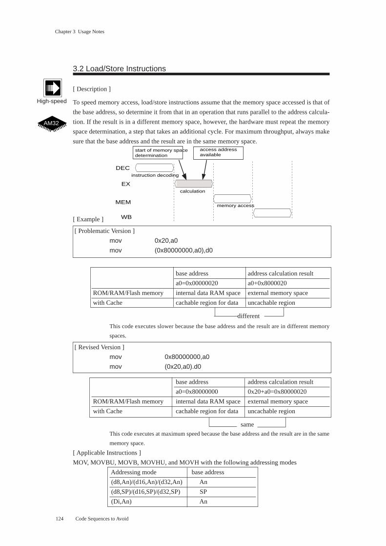
124
Chapter 3 Usage Notes
Code Sequences to Avoid
High-speed
AM32
calculation
memory access
DEC
MEM
EX
WB
instruction decoding
start of memory spacedetermination
access addressavailable
3.2 Load/Store Instructions
[ Description ]
To speed memory access, load/store instructions assume that the memory space accessed is that of
the base address, so determine it from that in an operation that runs parallel to the address calcula-
tion. If the result is in a different memory space, however, the hardware must repeat the memory
space determination, a step that takes an additional cycle. For maximum throughput, always make
sure that the base address and the result are in the same memory space.
[ Example ]
[ Problematic Version ]
mov 0x20,a0
mov (0x80000000,a0),d0
base address address calculation result
a0=0x00000020 a0+0x8000020
ROM/RAM/Flash memory internal data RAM space external memory space
with Cache cachable region for data uncachable region
different
This code executes slower because the base address and the result are in different memory
spaces.
[ Revised Version ]
mov 0x80000000,a0
mov (0x20,a0).d0
base address address calculation result
a0=0x80000000 0x20+a0=0x80000020
ROM/RAM/Flash memory internal data RAM space external memory space
with Cache cachable region for data uncachable region
same
This code executes at maximum speed because the base address and the result are in the same
memory space.
[ Applicable Instructions ]
MOV, MOVBU, MOVB, MOVHU, and MOVH with the following addressing modes
Addressing mode base address
(d8,An)/(d16,An)/(d32,An) An
(d8,SP)/(d16,SP)/(d32,SP) SP
(Di,An) An
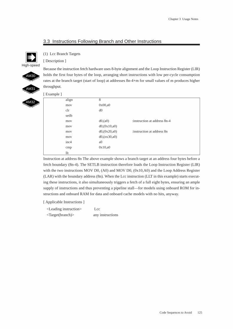
125
Chapter 3 Usage Notes
3.3 Instructions Following Branch and Other Instructions
(1) Lcc Branch Targets
[ Description ]
Because the instruction fetch hardware uses 8-byte alignment and the Loop Instruction Register (LIR)
holds the first four bytes of the loop, arranging short instructions with low per-cycle consumption
rates at the branch target (start of loop) at addresses 8n-4+m for small values of m produces higher
throughput.
[ Example ]
align 8
mov 0x00,a0
clr d0
setlb
mov d0,(a0) :instruction at address 8n-4
mov d0,(0x10,a0)
mov d0,(0x20,a0) :instruction at address 8n
mov d0,(ox30,a0)
inc4 a0
cmp 0x10,a0
llt
Instruction at address 8n The above example shows a branch target at an address four bytes before a
fetch boundary (8n-4). The SETLB instruction therefore loads the Loop Instruction Register (LIR)
with the two instructions MOV D0, (A0) and MOV D0, (0x10,A0) and the Loop Address Register
(LAR) with the boundary address (8n). When the Lcc instruction (LLT in this example) starts execut-
ing these instructions, it also simultaneously triggers a fetch of a full eight bytes, ensuring an ample
supply of instructions and thus preventing a pipeline stall—for models using onboard ROM for in-
structions and onboard RAM for data and onboard cache models with no hits, anyway.
[ Applicable Instructions ]
<Leading instruction> Lcc
<Target(branch)> any instructions
Code Sequences to Avoid
AM30
AM31
AM32
High-speed
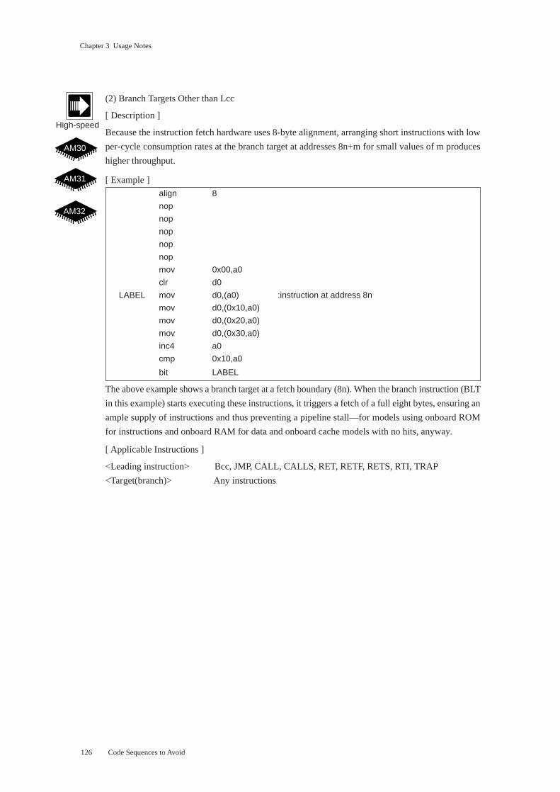
126
Chapter 3 Usage Notes
(2) Branch Targets Other than Lcc
[ Description ]
Because the instruction fetch hardware uses 8-byte alignment, arranging short instructions with low
per-cycle consumption rates at the branch target at addresses 8n+m for small values of m produces
higher throughput.
[ Example ]
align 8
nop
nop
nop
nop
nop
mov 0x00,a0
clr d0
LABEL mov d0,(a0) :instruction at address 8n
mov d0,(0x10,a0)
mov d0,(0x20,a0)
mov d0,(0x30,a0)
inc4 a0
cmp 0x10,a0
bit LABEL
The above example shows a branch target at a fetch boundary (8n). When the branch instruction (BLT
in this example) starts executing these instructions, it triggers a fetch of a full eight bytes, ensuring an
ample supply of instructions and thus preventing a pipeline stall—for models using onboard ROM
for instructions and onboard RAM for data and onboard cache models with no hits, anyway.
[ Applicable Instructions ]
<Leading instruction> Bcc, JMP, CALL, CALLS, RET, RETF, RETS, RTI, TRAP
<Target(branch)> Any instructions
High-speed
AM30
AM31
AM32
Code Sequences to Avoid
127
Chapter 3 Usage Notes
(3) Instructions Following Bcc or Lcc
[ Description ]
Arranging short instructions with low per-cycle consumption rates after a conditional branch in-
struction maximizes supply, producing higher throughput.
[ Example ]
blt LABEL
mul d0,d1 Two-byte instruction requiring multiple cycles to execute
The above example shows a MUL instruction executed when the branch instruction (BLT in this
example) fails. Because the instruction requires multiple cycles, the core has time to fetch more
instruction bytes, ensuring a better supply and thus higher throughput.
[ Applicable Instructions ]
< Leading instruction> Bcc or Lcc
<Target(branch)> Any instructions
(4 )Instructions Following Non-Branch Instructions
[ Description ]
Grouping long instructions together risks having instruction queue consumption outstrip supply.
For higher throughput, try to even out the consumption rate.
[ Example ]
mov 0x12345678,d0 six-byte instruction
mov (a0),d1 one byte instruction
inc d0 one byte instruction
add d0,d1 one byte instruction
mov 0x9abcdef0,d2 six-byte instruction
The above example shows such a separation. This arrangement evens out the consumption rate,
preventing pipeline stalls with the longer instructions and thus delivering higher throughput.
[ Applicable Instructions ]
<Leading instruction> Any instruction except Bcc, Lcc, JMP, CALL, CALLS, RET, RETF,
RETS, RTI,TRAP
<Target(branch) Any instructions
AM30
AM31
AM32
High-speed
AM30
AM31
AM32
High-speed
Code Sequences to Avoid
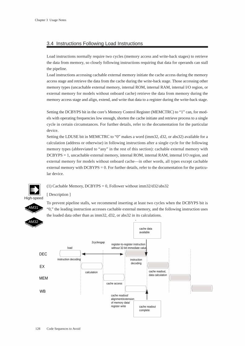
128
Chapter 3 Usage Notes
3.4 Instructions Following Load Instructions
Load instructions normally require two cycles (memory access and write-back stages) to retrieve
the data from memory, so closely following instructions requiring that data for operands can stall
the pipeline.
Load instructions accessing cachable external memory initiate the cache access during the memory
access stage and retrieve the data from the cache during the write-back stage. Those accessing other
memory types (uncachable external memory, internal ROM, internal RAM, internal I/O region, or
external memory for models without onboard cache) retrieve the data from memory during the
memory access stage and align, extend, and write that data to a register during the write-back stage.
Setting the DCBYPS bit in the core’s Memory Control Register (MEMCTRC) to “1” can, for mod-
els with operating frequencies low enough, shorten the cache initiate and retrieve process to a single
cycle in certain circumstances. For further details, refer to the documentation for the particular
device.
Setting the LDUSE bit in MEMCTRC to “0” makes a word (imm32, d32, or abs32) available for a
calculation (address or otherwise) in following instructions after a single cycle for the following
memory types (abbreviated to “any” in the rest of this section): cachable external memory with
DCBYPS = 1, uncachable external memory, internal ROM, internal RAM, internal I/O region, and
external memory for models without onboard cache—in other words, all types except cachable
external memory with DCBYPS = 0. For further details, refer to the documentation for the particu-
lar device.
(1) Cachable Memory, DCBYPS = 0, Follower without imm32/d32/abs32
[ Description ]
To prevent pipeline stalls, we recommend inserting at least two cycles when the DCBYPS bit is
“0,” the leading instruction accesses cachable external memory, and the following instruction uses
the loaded data other than as imm32, d32, or abs32 in its calculations.
High-speed
AM31
AM32
cache access
DEC
MEM
EX
WB
instruction decoding
calculation
2cyclesgap
instruction decoding
load
cache readout/alignment/extension of memory data/register write
cache data available
cache readout,data calculation
cache readout complete
register-to-register instruction without 32-bit immediate value
Code Sequences to Avoid
129
Chapter 3 Usage Notes
[ Example ]
Problematic Version
inc a2
mov (a0),d0 : Load instruction
inc a3
add d1,d0 : Instruction using loaded data other than as imm32, d32 or abs32
or
inc a2
inc a3
mov (a0),d0 : Load instruction
add d1,d0 I: nstruction using loaded data other than as imm32, d32 or abs32
Retrieving and aligning the data from the cache takes two cycles, so the pipeline stalls until
the data loaded with the MOV instruction is available to the ADD instruction.
Revised Version
mov (a0),d0 : Load instruction
inc a2
inc a3
add d1,d0 : Instruction using loaded data other than as imm32, d32 or abs32
The data loaded with the MOV instruction is available to the ADD instruction, so the pipeline
does not stall.
[ Applicable Instructions ]
<Leading instruction> All load variants of MOV, MOVBU, MOVB,* MOVHU, and MOVH*
(* The MOVB Mem, Reg and MOVH Mem, Reg variants require only a one-
cycle gap.)
<Following instruction> Any instruction using the loaded data other than as imm32, d32, or abs32 in its
calculations except the following; MOV PSW,Dn, MOV Dm,PSW,
AND imm16,PSW, OR imm16,PSW, Bcc, Lcc, JMP, TRAP, NOP.
Here cachable external memory refers to the cachable portions of AM31 or AM32 external
memory.
Code Sequences to Avoid
130
Chapter 3 Usage Notes
(2) Cachable Memory, DCBYPS = 0, Follower with d32
[ Description ]
To prevent pipeline stalls, we recommend inserting at least one cycle when the DCBYPS bit is “0,”
the leading instruction accesses cachable external memory, and the following instruction uses the
data together with a 32-bit displacement [imm32?] operand.
[ Example ]
[ Problematic Version ]
inc a1
mov (a0),d0 Load instruction
add 0x12345678,d0 Instruction using loaded data and 32-bit
displacement d32 operand
Retrieving and aligning the data from the cache takes one cycle, so the pipeline stalls
until the data loaded with the MOV instruction is available to the ADD instruction.
[ Revised Version ]
mov (a0),d0 Load instruction
inc a1
add 0x12345678,d0 Instruction using loaded data and 32-bit
displacement d32 operand
The data loaded with the MOV instruction is available to the ADD instruction, so the
pipeline does not stall.
[ Applicable Instructions ]
<Leading instruction> All load variants of MOV, MOVBU, and MOVHU
<Following instruction> MOV, MOVBU, and MOVHU variants with 32-bit operands (d32).
Here cachable external memory refers to the cachable portions of AM31 or AM32
external memory.
Code Sequences to Avoid
High-speed
AM31
AM32
cache access
DEC
MEM
EX
WB
instruction decoding
calculation
1cycle gap
instruction decoding
load
cache readout/alignment/extension of memory data/register write
cache data available
cache readout,data calculation
cache readout complete
register-to-register instruction with 32-bit immediate value
32-bit immediate value read
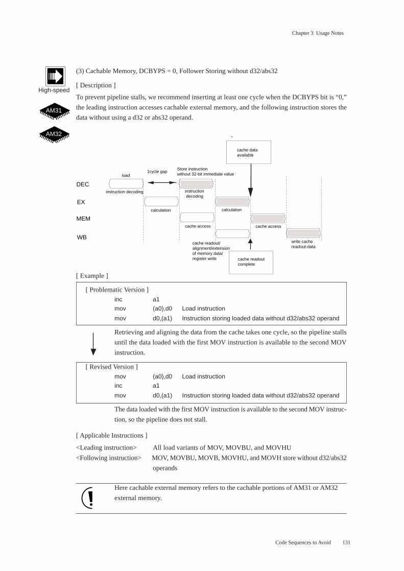
131
Chapter 3 Usage Notes
(3) Cachable Memory, DCBYPS = 0, Follower Storing without d32/abs32
[ Description ]
To prevent pipeline stalls, we recommend inserting at least one cycle when the DCBYPS bit is “0,”
the leading instruction accesses cachable external memory, and the following instruction stores the
data without using a d32 or abs32 operand.
[ Example ]
[ Problematic Version ]
inc a1
mov (a0),d0 Load instruction
mov d0,(a1) Instruction storing loaded data without d32/abs32 operand
Retrieving and aligning the data from the cache takes one cycle, so the pipeline stalls
until the data loaded with the first MOV instruction is available to the second MOV
instruction.
[ Revised Version ]
mov (a0),d0 Load instruction
inc a1
mov d0,(a1) Instruction storing loaded data without d32/abs32 operand
The data loaded with the first MOV instruction is available to the second MOV instruc-
tion, so the pipeline does not stall.
[ Applicable Instructions ]
<Leading instruction> All load variants of MOV, MOVBU, and MOVHU
<Following instruction> MOV, MOVBU, MOVB, MOVHU, and MOVH store without d32/abs32
operands
Here cachable external memory refers to the cachable portions of AM31 or AM32
external memory.
Code Sequences to Avoid
High-speed
AM31
AM32
cache access
DEC
MEM
EX
WB
instruction decoding
calculation
1cycle gap
instruction decoding
load
cache readout/alignment/extension of memory data/register write
cache data available
write cache readout-data
cache readout complete
Store instruction without 32-bit immediate value
cache access
calculation
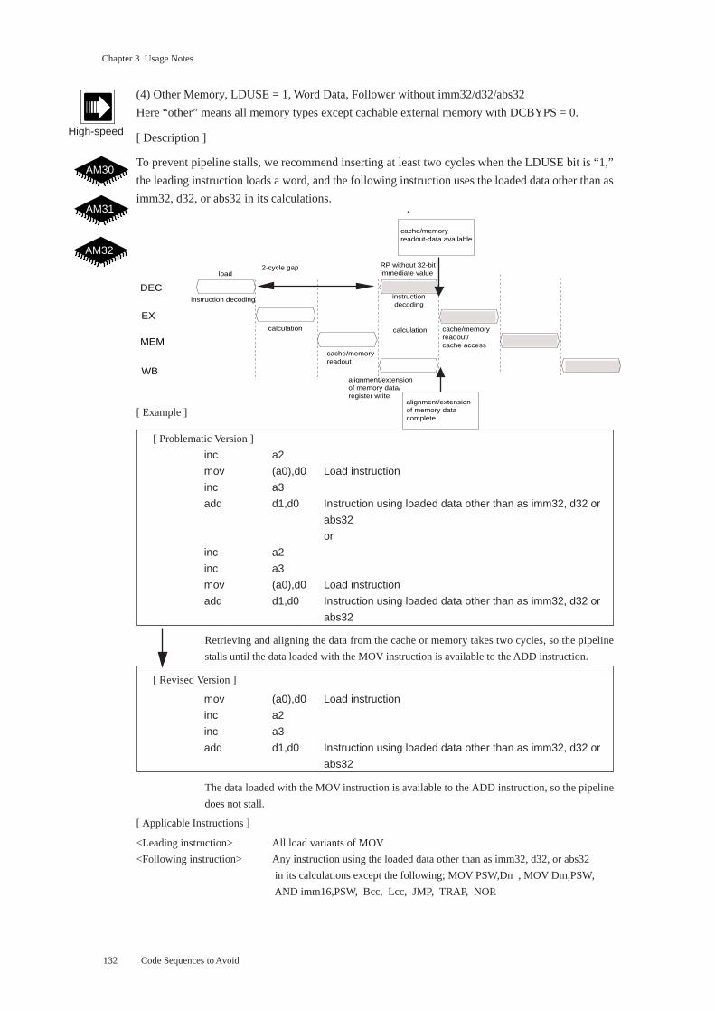
132
Chapter 3 Usage Notes
(4) Other Memory, LDUSE = 1, Word Data, Follower without imm32/d32/abs32
Here “other” means all memory types except cachable external memory with DCBYPS = 0.
[ Description ]
To prevent pipeline stalls, we recommend inserting at least two cycles when the LDUSE bit is “1,”
the leading instruction loads a word, and the following instruction uses the loaded data other than as
imm32, d32, or abs32 in its calculations.
[ Example ]
[ Problematic Version ]
inc a2
mov (a0),d0 Load instruction
inc a3
add d1,d0 Instruction using loaded data other than as imm32, d32 or
abs32
or
inc a2
inc a3
mov (a0),d0 Load instruction
add d1,d0 Instruction using loaded data other than as imm32, d32 or
abs32
Retrieving and aligning the data from the cache or memory takes two cycles, so the pipeline
stalls until the data loaded with the MOV instruction is available to the ADD instruction.
[ Revised Version ]
mov (a0),d0 Load instruction
inc a2
inc a3
add d1,d0 Instruction using loaded data other than as imm32, d32 or
abs32
The data loaded with the MOV instruction is available to the ADD instruction, so the pipeline
does not stall.
[ Applicable Instructions ]
<Leading instruction> All load variants of MOV
<Following instruction> Any instruction using the loaded data other than as imm32, d32, or abs32
in its calculations except the following; MOV PSW,Dn , MOV Dm,PSW,
AND imm16,PSW, Bcc, Lcc, JMP, TRAP, NOP.
Code Sequences to Avoid
cache/memoryreadout
DEC
MEM
EX
WB
instruction decoding
calculation
2-cycle gap
instruction decoding
load
alignment/extension of memory data/register write
cache/memory readout-data available
alignment/extension of memory data complete
RP without 32-bit immediate value
cache/memory readout/cache access
calculation
AM30
AM31
AM32
High-speed
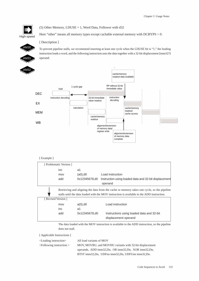
133
Chapter 3 Usage Notes
(5) Other Memory, LDUSE = 1, Word Data, Follower with d32
Here “other” means all memory types except cachable external memory with DCBYPS = 0.
[ Description ]
To prevent pipeline stalls, we recommend inserting at least one cycle when the LDUSE bit is “1,” the leading
instruction loads a word, and the following instruction uses the data together with a 32-bit displacement [imm32?]
operand.
[ Example ]
[ Problematic Version ]
inc a1
mov (a0),d0 Load instruction
add 0x12345678,d0 Instruction using loaded data and 32-bit displacement
operand
Retrieving and aligning the data from the cache or memory takes one cycle, so the pipeline
stalls until the data loaded with the MOV instruction is available to the ADD instruction.
[ Revised Version ]
mov a(0),d0 Load instruction
inc a1
add 0x12345678,d0 Instructions using loaded data and 32-bit
displacement operand
The data loaded with the MOV instruction is available to the ADD instruction, so the pipeline
does not stall.
[ Applicable Instructions ]
<Leading instruction> All load variants of MOV
<Following instruction > MOV, MOVBU, and MOVHU variants with 32-bit displacement
operands, ADD imm32,Dn, OR imm32,Dn, XOR imm32,Dn,
BTST imm32,Dn, UDFnn imm32,Dn, UDFUnn imm32,Dn.
Code Sequences to Avoid
High-speed
AM30
AM31
AM32
cache/memoryreadout
DEC
MEM
EX
WB
instruction decoding
calculation
1 cycle gap
instruction decoding
load
alignment/extension of memory data/register write
cache/memory readout-data available
alignment/extension of memory data complete
RP without 32-bit immediate value
cache/memory readout/cache access
32-bit immediate value readout
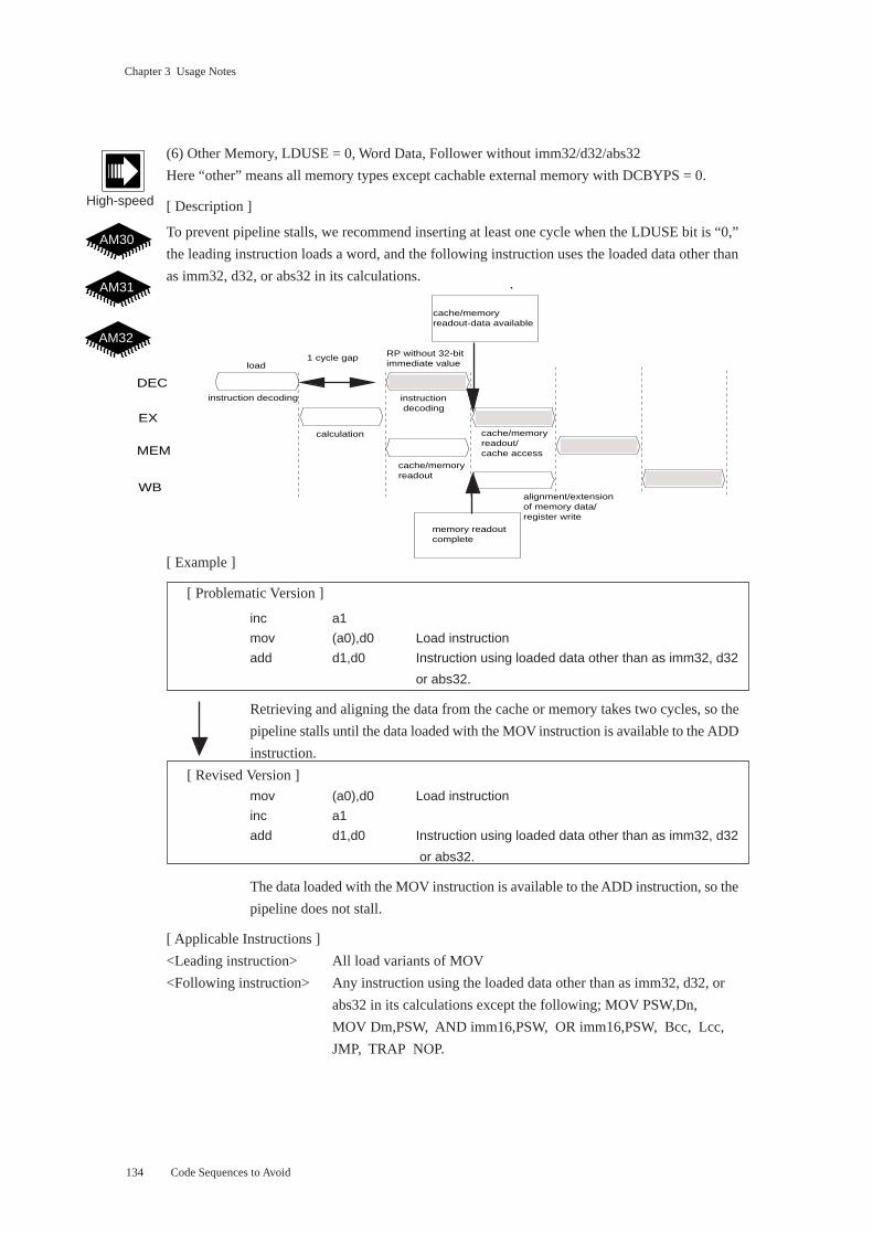
134
Chapter 3 Usage Notes
(6) Other Memory, LDUSE = 0, Word Data, Follower without imm32/d32/abs32
Here “other” means all memory types except cachable external memory with DCBYPS = 0.
[ Description ]
To prevent pipeline stalls, we recommend inserting at least one cycle when the LDUSE bit is “0,”
the leading instruction loads a word, and the following instruction uses the loaded data other than
as imm32, d32, or abs32 in its calculations.
[ Example ]
[ Problematic Version ]
inc a1
mov (a0),d0 Load instruction
add d1,d0 Instruction using loaded data other than as imm32, d32
or abs32.
Retrieving and aligning the data from the cache or memory takes two cycles, so the
pipeline stalls until the data loaded with the MOV instruction is available to the ADD
instruction.
[ Revised Version ]
mov (a0),d0 Load instruction
inc a1
add d1,d0 Instruction using loaded data other than as imm32, d32
or abs32.
The data loaded with the MOV instruction is available to the ADD instruction, so the
pipeline does not stall.
[ Applicable Instructions ]
<Leading instruction> All load variants of MOV
<Following instruction> Any instruction using the loaded data other than as imm32, d32, or
abs32 in its calculations except the following; MOV PSW,Dn,
MOV Dm,PSW, AND imm16,PSW, OR imm16,PSW, Bcc, Lcc,
JMP, TRAP NOP.
Code Sequences to Avoid
AM30
AM31
AM32
High-speed
cache/memoryreadout
DEC
MEM
EX
WB
instruction decoding
calculation
1 cycle gap
instruction decoding
load
alignment/extension of memory data/register write
cache/memory readout-data available
memory readoutcomplete
RP without 32-bit immediate value
cache/memory readout/cache access
135
Chapter 3 Usage Notes
(7) Other Memory, Non-Word Data, Follower without imm32/d32/abs32
Here “other” means all memory types except cachable external memory with DCBYPS = 0.
[ Description ]
To prevent pipeline stalls, we recommend inserting at least two cycles when the leading instruction
loads a byte or half-word, and the following instruction uses the loaded data other than as imm32,
d32, or abs32 in its calculations.
[ Example ]
[ Problematic Version ]
inc a1
movbu (a0),d0 Load instruction
inc a2
add d1,d0 Instruction using loaded data other than as imm32, d32
or
abs32
or
inc a1
inc a2
movbu (a0),d0 Load instruction
add d1,d0 Instruction using loaded data other than as imm32, d32
or abs32
Retrieving and aligning the data from the cache or memory takes two cycles, so the
pipeline stalls until the data loaded with the MOV instruction is available to the ADD
instruction.
[ Revised Version ]
movbu (a0),d0 Load instruction
inc a1
inc a2
add d1,d0 Instruction using loaded data other than as imm32, d32 or abs32.
The data loaded with the MOV instruction is available to the ADD instruction, so the
pipeline does not stall.
Code Sequences to Avoid
cache/memoryreadout
DEC
MEM
EX
WB
instruction decoding
calculation
2-cycle gap
instruction decoding
load
alignment/extension of memory data/register write
memory readout-data available
alignment/extensioncomplete
RP without 32-bit immediate value
cache/memory readout/cache access
High-speed
AM30
AM31
AM32
136
Chapter 3 Usage Notes
[ Applicable Instructions ]
<Leading instruction> All load variants of MOV, MOVBU, MOVB,* MOVHU, and
MOVH* (* The MOVB Mem, Reg and MOVH Mem, Reg variants
require only a one-cycle gap.)
<Following instruction> Any instruction using the loaded data other than as imm32, d32, or
abs32 in its calculations except the following; MOV PSW,Dn,
MOV Dm,PSW, AND imm16,PSW, OR imm16,PSW, Bcc, Lcc, JMP,
TRAP, NOP.
Code Sequences to Avoid
137
Chapter 3 Usage Notes
(8) Other Memory, Non-Word Data, Follower with d32
Here “other” means all memory types except cachable external memory with DCBYPS = 0.
[ Description ]
To prevent pipeline stalls, we recommend inserting at least one cycle when the leading instruction
loads a byte or half-word, and the following instruction uses the data together with a 32-bit displace-
ment [imm32?] operand.
[ Example ]
[ Problematic Version ]
inc a1
movbu (a0),d0 Load instruction
add 0x12345678,d0 Instruction using loaded data and 32-bit
displacement operand
Retrieving and aligning the data from the cache or memory takes one cycle, so the
pipeline stalls until the data loaded with the MOVBU instruction is available to the
ADD instruction.
[ Revised Version ]
movbu (a0),d0 Load instruction
inc a1
add 0x12345678,d0 Instruction using loaded data and 32-bit
displacement operand
The data loaded with the MOVBU instruction is available to the ADD instruction, so
the pipeline does not stall.
[ Applicable Instructions ]
<Leading instruction> All load variants of MOVBU and MOVHU
<Following instruction> MOVBU, MOVBU, and MOVHU variants with 32-bit displacement
operands; ADD imm32,Dn/An/SP, SUB imm32,Dn/An,
CMP imm32,Dn/An, AND imm32,Dn, OR imm32,Dn,
XOR imm32,Dn, BTST imm32,Dn, UDFnn imm32,Dn,
UDFUnn imm32,Dn
Code Sequences to Avoid
AM30
AM31
AM32
cache/memoryreadout
DEC
MEM
EX
WB
instruction decoding
calculation
1 cycle gap
instruction decoding
load
alignment/extension of memory data/register write
cache/memory readout-data available
alignment/extension of memory data complete
RP without 32-bit immediate value
cache/memory readout/cache access
32-bit immediate value readout
High-speed
138
Chapter 3 Usage Notes
(9) Other Memory, Follower Storing without d32/abs32
Here “other” means all memory types except cachable external memory with DCBYPS = 0.
[ Description ]
To prevent pipeline stalls, we recommend inserting at least one cycle when the following instruction
stores the data without using a d32 or abs32 operand.
[ Example ]
[ Problematic Version ]
inc a1
movbu(a0),d0 Load instruction
mov d0,(a1) Instruction storing loaded data without d32/abs32 operand
Retrieving and aligning the data from the cache or memory takes one cycle, so the
pipeline stalls until the data loaded with the MOVBU instruction is available to the
MOV instruction.
[ Revised Version ]
movbu (a0),d0 Load instruction
inc a1
mov d0,(a1) Instruction storing loaded data without d32/abs32 operand
The data loaded with the MOVBU instruction is available to the MOV instruction, so
the pipeline does not stall.
[ Applicable Instructions ]
<Leading instruction> All load variants of MOVBU and MOVHU
<Following instruction> MOV, MOVBU, MOVB, MOVHU, and MOVH store without d32/
abs32 operands.
Code Sequences to Avoid
AM30
AM31
AM32
High-speed
cache/memoryreadout
DEC
MEM
EX
WB
instruction decoding
calculation
1 cycle gap
instruction decoding
load
alignment/extension of memory data/register write
cache/memory readout-data available
alignment/extension of memory data complete
Store instruction without 32-bit immediate value
cache/memory readout/data calculation
calculation
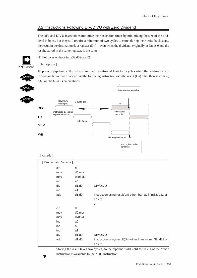
139
Chapter 3 Usage Notes
3.5 Instructions Following DIV/DIVU with Zero Dividend
The DIV and DIVU instructions minimize their execution times by minimizing the size of the divi-
dend in bytes, but they still require a minimum of two cycles to store, during their write-back stage,
the result in the destination data register (Dn)—even when the dividend, originally in Dn, is 0 and the
result, stored in the same register, is the same.
(1) Follower without imm32/d32/abs32
[ Description ]
To prevent pipeline stalls, we recommend inserting at least two cycles when the leading divide
instruction has a zero dividend and the following instruction uses the result (Dn) other than as imm32,
d32, or abs32 in its calculations.
[ Example ]
[ Problematic Version ]
clr d0
mov d0,mdr
mov 0x05,d1
inc a0
div d1,d0 DIV/DIVU
inc a1
add d1,d0 Instruction using result(dn) other than as imm32, d32 or
abs32
or
clr d0
mov d0,mdr
mov 0x05,d1
inc a0
inc a0
inc a1
div d1,d0 DIV/DIVU
add d1,d0 Instruction using result(Dn) other than as imm32, d32 or
abs32
Storing the result takes two cycles, so the pipeline stalls until the result of the divide
instruction is available to the ADD instruction.
Code Sequences to Avoid
DEC
MEM
EX
WB
instruction decodingregister readout
calculation
2-cycle gap
instruction decoding
DIV/DIVUfinal cycle
data register write
data register available
data register write complete
RR
High-speed
AM30
AM31
AM32
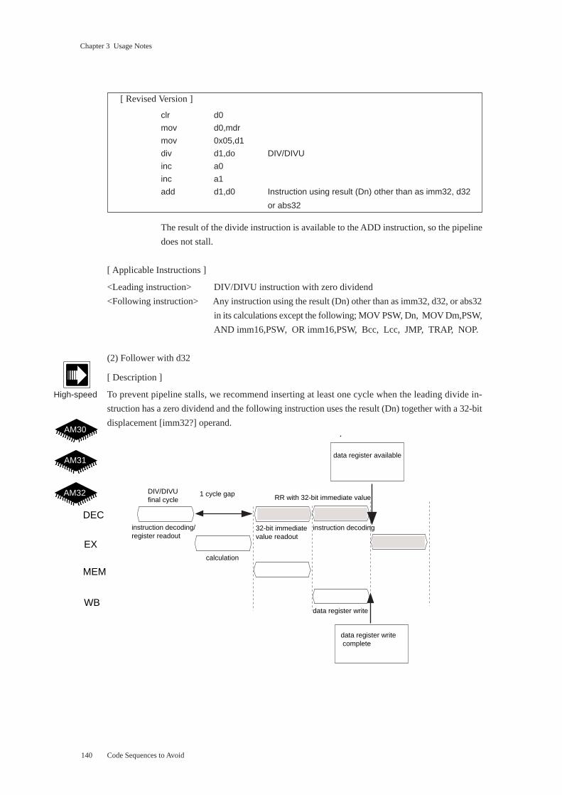
140
Chapter 3 Usage Notes
[ Revised Version ]
clr d0
mov d0,mdr
mov 0x05,d1
div d1,do DIV/DIVU
inc a0
inc a1
add d1,d0 Instruction using result (Dn) other than as imm32, d32
or abs32
The result of the divide instruction is available to the ADD instruction, so the pipeline
does not stall.
[ Applicable Instructions ]
<Leading instruction> DIV/DIVU instruction with zero dividend
<Following instruction> Any instruction using the result (Dn) other than as imm32, d32, or abs32
in its calculations except the following; MOV PSW, Dn, MOV Dm,PSW,
AND imm16,PSW, OR imm16,PSW, Bcc, Lcc, JMP, TRAP, NOP.
(2) Follower with d32
[ Description ]
To prevent pipeline stalls, we recommend inserting at least one cycle when the leading divide in-
struction has a zero dividend and the following instruction uses the result (Dn) together with a 32-bit
displacement [imm32?] operand.
Code Sequences to Avoid
DEC
MEM
EX
WB
instruction decoding/register readout
calculation
1 cycle gap
instruction decoding
DIV/DIVUfinal cycle
data register write
data register available
data register write complete
RR with 32-bit immediate value
32-bit immediatevalue readout
AM30
AM31
AM32
High-speed
141
Chapter 3 Usage Notes
[ Example ]
[ Problematic Version ]
clr d0
mov d0,mdr
mov 0x05,d1
inc a0
div d1,d0 DIV/DIVU
add 0x12345678,d0 Instruction using result(Dn) and 32-bit
displacement operand
Storing the result takes one cycle, so the pipeline stalls until the result of the divide
instruction is available to the ADD instruction.
[ Revised Version ]
clr d0
mov d0,mdr
mov 0x05,d1
div d1,d0 DIV/DIVU
inc a0
add 0x12345678,d0 Instruction using result(dn) and 32-bit displacement
operand
The result of the divide instruction is available to the ADD instruction, so the pipeline
does not stall.
[ Applicable Instructions ]
<Leading instruction> DIV/DIVU instruction with zero dividend
<Following instruction> MOV, MOVBU, and MOVHU variants with 32-bit displacement
operands; ADD imm32,Dn/An/SP, SUB imm32,Dn/An,
CMP imm32,Dn/An, AND imm32,Dn, OR imm32,Dn,
XOR imm32,Dn, BTST imm32,Dn, UDFnn imm32,Dn,
UDFUnn imm32,Dn
Code Sequences to Avoid
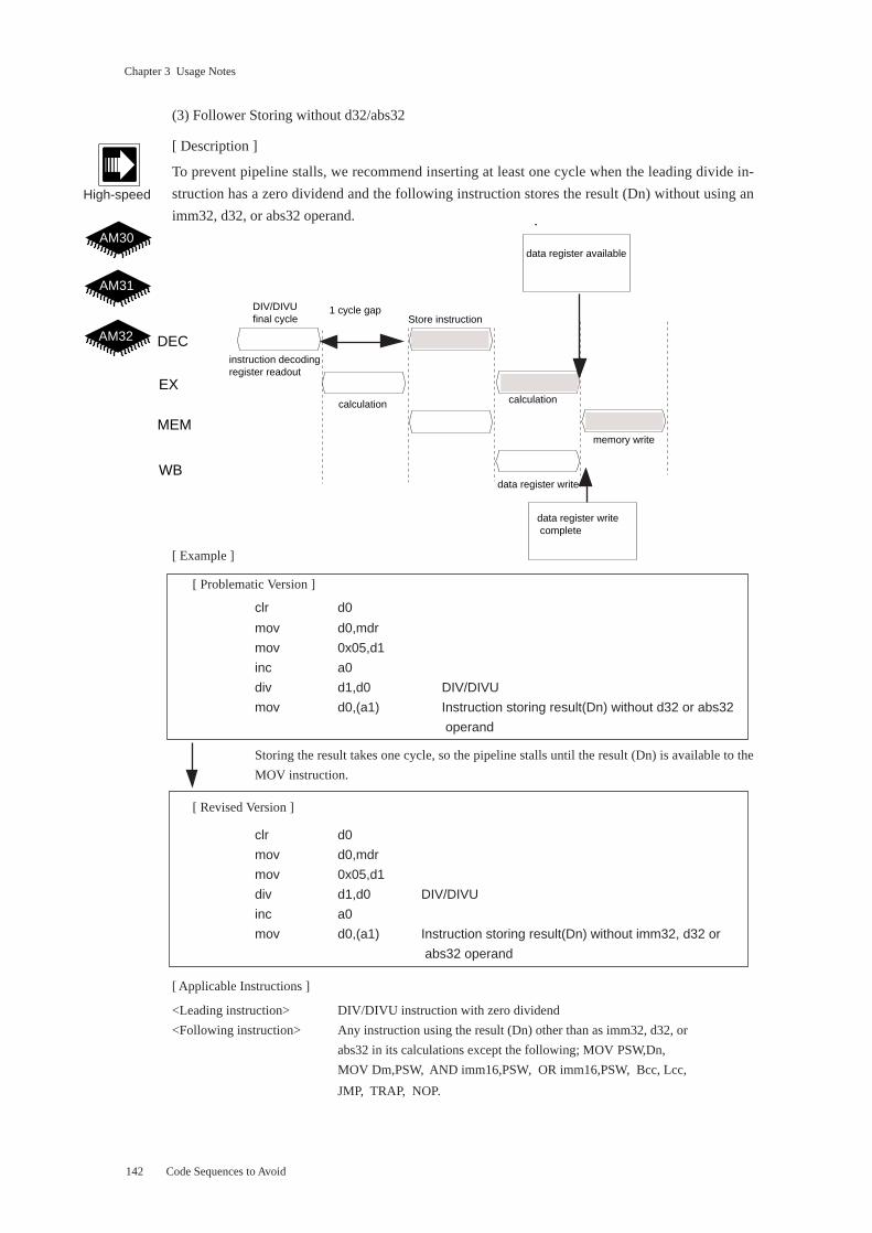
142
Chapter 3 Usage Notes
(3) Follower Storing without d32/abs32
[ Description ]
To prevent pipeline stalls, we recommend inserting at least one cycle when the leading divide in-
struction has a zero dividend and the following instruction stores the result (Dn) without using an
imm32, d32, or abs32 operand.
[ Example ]
[ Problematic Version ]
clr d0
mov d0,mdr
mov 0x05,d1
inc a0
div d1,d0 DIV/DIVU
mov d0,(a1) Instruction storing result(Dn) without d32 or abs32
operand
Storing the result takes one cycle, so the pipeline stalls until the result (Dn) is available to the
MOV instruction.
[ Revised Version ]
clr d0
mov d0,mdr
mov 0x05,d1
div d1,d0 DIV/DIVU
inc a0
mov d0,(a1) Instruction storing result(Dn) without imm32, d32 or
abs32 operand
[ Applicable Instructions ]
<Leading instruction> DIV/DIVU instruction with zero dividend
<Following instruction> Any instruction using the result (Dn) other than as imm32, d32, or
abs32 in its calculations except the following; MOV PSW,Dn,
MOV Dm,PSW, AND imm16,PSW, OR imm16,PSW, Bcc, Lcc,
JMP, TRAP, NOP.
Code Sequences to Avoid
AM30
AM31
AM32
High-speed
DEC
MEM
EX
WB
instruction decodingregister readout
calculation
1 cycle gapDIV/DIVUfinal cycle
data register write
data register available
data register write complete
Store instruction
calculation
memory write
143
Chapter 3 Usage Notes
3.6 Instructions Preceding Lcc
The Lcc instruction bypasses the five-stage pipeline with additional hardware to increase the execution
speed. To ensure proper interaction between the two, it must therefore wait for certain preceding instructions
to complete.
(1) SETLB
[ Description ]
To ensure smooth pipeline operation, we recommend inserting at least three cycles between the Lcc instruc-
tion and the preceding SETLB instruction setting up the two registers that it must reference: Loop Instruc-
tion Register (LIR) and Loop Address (LAR) Register.
[ Example ]
[ Problematic Version ]
inc d0
setlb SETLB
inc d1
inc d2
lgt Lcc or
inc d0
inc d1
setlb SETLB
inc d2
lgt Lcc or
inc d0
inc d1
inc d2
setlb SETLB
lgt Lcc
Loading the LIR and LAR registers takes three cycles, so the pipeline stalls until their con-
tents are available to the LGT instruction.
Code Sequences to Avoid
LIR write
DEC
MEM
EX
WB
instruction decoding instruction decoding/LIR/LAR readout
LAR write
3-cycle gap
SETLB complete
Lcc available
144
Chapter 3 Usage Notes
[ Revised Version ]
setlb SETLB
ubc d0
inc d1
inc d2
lgt Lcc
The updated contents of the LIR and LAR registers are available to the LGT
instruction, so the pipeline does not stall.
[ Applicable Instructions ]
<Leading instruction> SETLB
<Following instruction> Lcc
(2) Other Instructions Modifying LIR and LAR
[ Description ]
To ensure smooth pipeline operation, we recommend inserting at least three cycles between the Lcc
instruction and other preceding instructions (MOVM, RET, and RETF) modifying the two registers
that it must reference: Loop Instruction Register (LIR) and Loop Address (LAR) Register.
Code Sequences to Avoid
calculation
DEC
MEM
EX
WB
instruction decoding instruction decoding/LIR/LAR readout
Lcc3-cycle gap
SETLB complete
LAR readout available
MOVM/RET/RETFfinal cycle
memory readout
LAR write
145
Chapter 3 Usage Notes
[ Example ]
[ Problematic Version ]
inc d0
movm (sp),[other] Instruction modifying LIR and LAR
inc d1
inc d2
lgt Lcc or
inc d0
inc d1
movm (sp),[other] Instruction modifying LIR and LAR
inc d2
lgt Lcc or
inc d0
inc d1
inc d2
movm (sp),pother] Instruction modifying LIE and LAE
lgt Lcc
Loading the LIR and LAR registers takes three cycles, so the pipeline stalls until their
contents are available to the LGT instruction.
[ Revised Version ]
movm (sp),[other] Instruction modifying LIR and LAR
inc d0
inc d1
inc d2
lgt Lcc
The updated contents of the LIR and LAR registers are available to the LGT instruction,
so the pipeline does not stall.
[ Applicable Instructions ]
<Leading instruction> MOVM (SP),regs, RET, RETF
<Following instruction> Lcc
Code Sequences to Avoid
146
Chapter 3 Usage Notes
Code Sequences to Avoid
High-speed
AM31
AM30
AM32
calculation
DEC
MEM
EX
WB
instruction decoding
SETLB1 cycle gap
LIR/LAR writein parallel
SETLB available
MOVM/RET/RETFfinal cycle
memory readout
LIR write
instruction decoding
LAR write
3.7 Instructions Preceding SETLB
The SETLB instruction bypasses the five-stage pipeline with additional hardware to increase the
execution speed. To ensure proper interaction between the two, it must wait for preceding instruc-
tions (MOVM, RET, and RETF) modifying the two registers that it loads: Loop Instruction Register
(LIR) and Loop Address (LAR) Register.
[ Description ]
To ensure smooth pipeline operation, we therefore recommend inserting at least one cycle between
such instructions and the SETLB instruction.
[ Example ]
[ Problematic Version ]
inc d0
movm (sp),[other] Instruction modifying LIR and LAR
setlb SETLB
Loading the LIR and LAR registers takes one cycle, so the pipeline stalls until their
contents are available to the SETLB instruction.
[ Revised Version ]
movm (sp),[other] Instruction modifying LIR and LAR
inc d0
setlb SETLB
The updated contents of the LIR and LAR registers are available to the SETLB in-
struction, so the pipeline does not stall.
[ Applicable Instructions ]
<Leading instruction> MOVM (SP),regs; RET; RETF
<Following instruction> SETLB
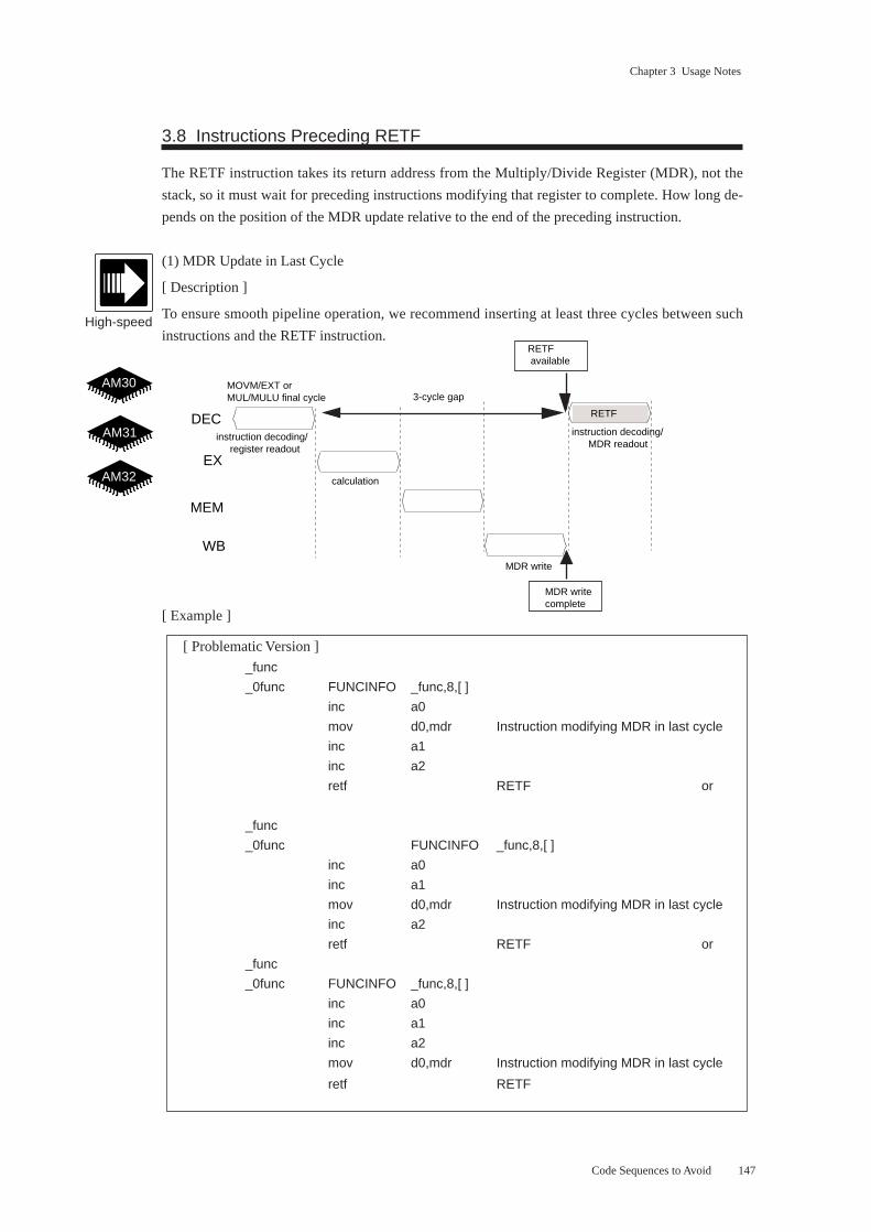
147
Chapter 3 Usage Notes
3.8 Instructions Preceding RETF
The RETF instruction takes its return address from the Multiply/Divide Register (MDR), not the
stack, so it must wait for preceding instructions modifying that register to complete. How long de-
pends on the position of the MDR update relative to the end of the preceding instruction.
(1) MDR Update in Last Cycle
[ Description ]
To ensure smooth pipeline operation, we recommend inserting at least three cycles between such
instructions and the RETF instruction.
[ Example ]
[ Problematic Version ]
_func
_0func FUNCINFO _func,8,[ ]
inc a0
mov d0,mdr Instruction modifying MDR in last cycle
inc a1
inc a2
retf RETF or
_func
_0func FUNCINFO _func,8,[ ]
inc a0
inc a1
mov d0,mdr Instruction modifying MDR in last cycle
inc a2
retf RETF or
_func
_0func FUNCINFO _func,8,[ ]
inc a0
inc a1
inc a2
mov d0,mdr Instruction modifying MDR in last cycle
retf RETF
calculation
DEC
MEM
EX
WB
instruction decoding/ register readout
RETF
3-cycle gap
MDR writecomplete
RETF available
MOVM/EXT orMUL/MULU final cycle
MDR write
instruction decoding/ MDR readout
High-speed
AM31
AM30
AM32
Code Sequences to Avoid
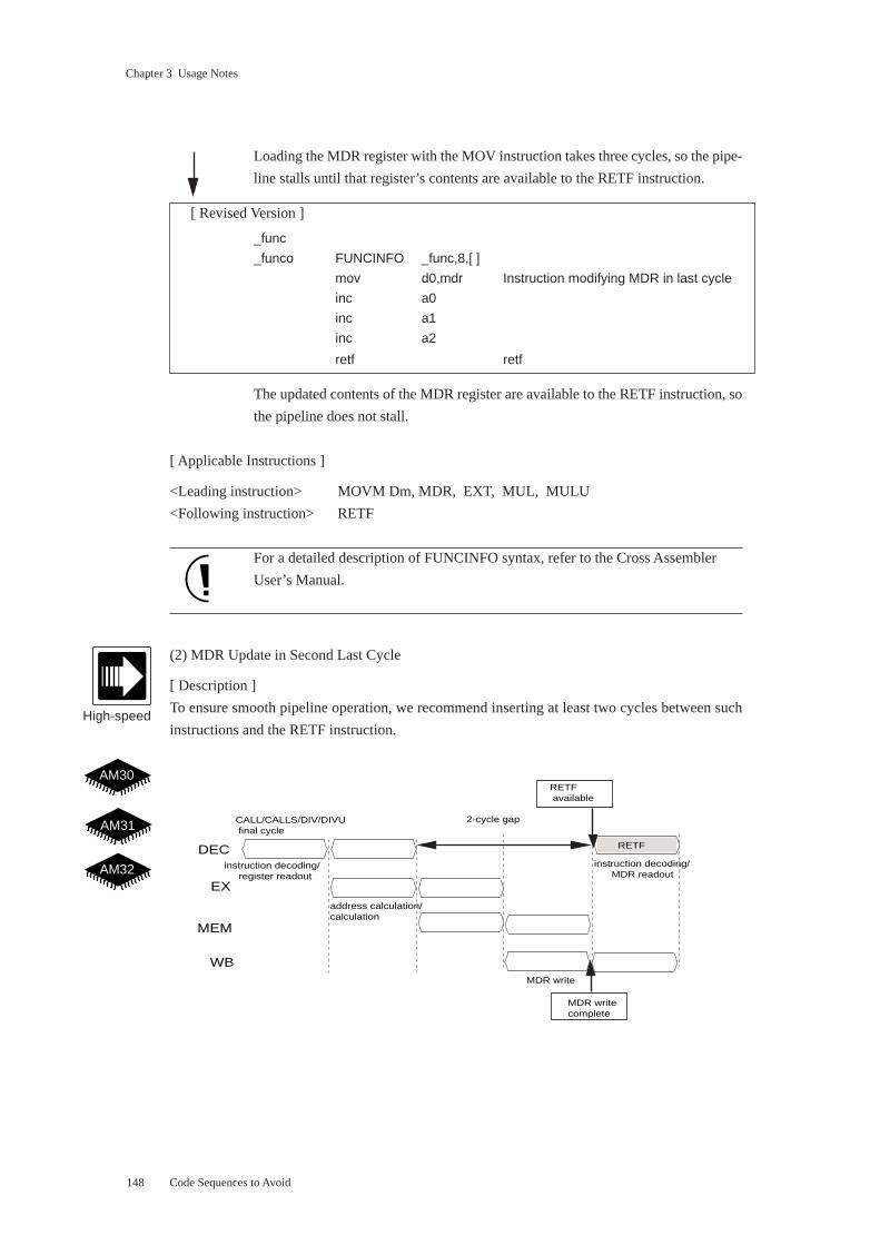
148
Chapter 3 Usage Notes
Loading the MDR register with the MOV instruction takes three cycles, so the pipe-
line stalls until that register’s contents are available to the RETF instruction.
[ Revised Version ]
_func
_funco FUNCINFO _func,8,[ ]
mov d0,mdr Instruction modifying MDR in last cycle
inc a0
inc a1
inc a2
retf retf
The updated contents of the MDR register are available to the RETF instruction, so
the pipeline does not stall.
[ Applicable Instructions ]
<Leading instruction> MOVM Dm, MDR, EXT, MUL, MULU
<Following instruction> RETF
For a detailed description of FUNCINFO syntax, refer to the Cross Assembler
User’s Manual.
(2) MDR Update in Second Last Cycle
[ Description ]
To ensure smooth pipeline operation, we recommend inserting at least two cycles between such
instructions and the RETF instruction.
address calculation/calculation
DEC
MEM
EX
WB
instruction decoding/ register readout
RETF
2-cycle gap
MDR writecomplete
RETF available
CALL/CALLS/DIV/DIVU final cycle
MDR write
instruction decoding/ MDR readout
High-speed
AM31
AM30
AM32
Code Sequences to Avoid
149
Chapter 3 Usage Notes
[ Example ]
[ Problematic Version ]
_lab
LABEL FUNCINFO _lab,8,[ ]
inc a0
div d1,d0 Instruction modifyint MDR in second last cycle
inc a1
retf RETF or
_lab
LABEL FUNCINFO _lab,8,[ ]
inc a0
inc a1
div d1,d0 Instruction modifying MDR in second last cycle
retf RETF
Updating the MDR register with the DIV instruction takes two cycles, so the pipeline stalls
until that register’s contents are available to the RETF instruction.
Revised Version
_lab
LABEL FUNCINFO _lab,8,[ ]
div d1,d0 Instruction modifying MDR in second last cycle
inc a0
inc a1
retf RETF
The updated contents of the MDR register are available to the RETF instruction, so the pipe-
line does not stall.
Applicable Instructions
<Leading instruction> DIV, DIVU, CALL, CALLS
<Following instruction> RETF
For a detailed description of FUNCINFO syntax, refer to the Cross Assembler User’s
Manual.
Code Sequences to Avoid
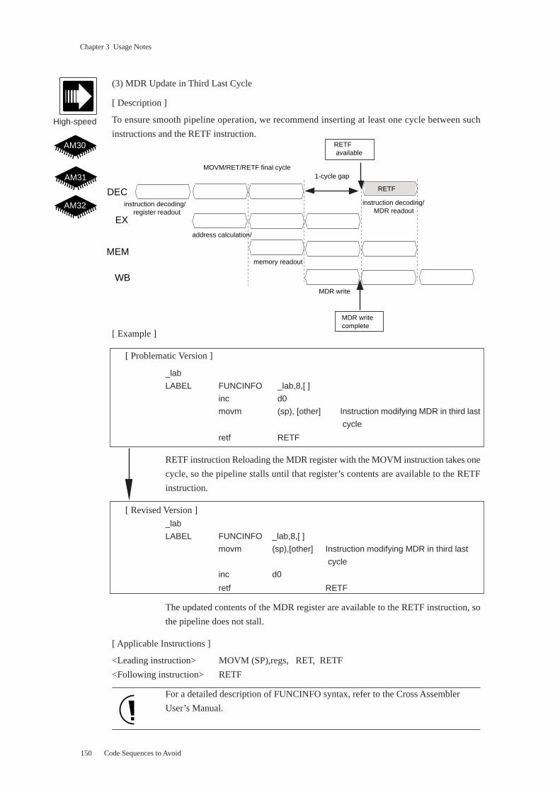
150
Chapter 3 Usage Notes
(3) MDR Update in Third Last Cycle
[ Description ]
To ensure smooth pipeline operation, we recommend inserting at least one cycle between such
instructions and the RETF instruction.
[ Example ]
[ Problematic Version ]
_lab
LABEL FUNCINFO _lab,8,[ ]
inc d0
movm (sp), [other] Instruction modifying MDR in third last
cycle
retf RETF
RETF instruction Reloading the MDR register with the MOVM instruction takes one
cycle, so the pipeline stalls until that register’s contents are available to the RETF
instruction.
[ Revised Version ]
_lab
LABEL FUNCINFO _lab,8,[ ]
movm (sp),[other] Instruction modifying MDR in third last
cycle
inc d0
retf RETF
The updated contents of the MDR register are available to the RETF instruction, so
the pipeline does not stall.
[ Applicable Instructions ]
<Leading instruction> MOVM (SP),regs, RET, RETF
<Following instruction> RETF
For a detailed description of FUNCINFO syntax, refer to the Cross Assembler
User’s Manual.
Code Sequences to Avoid
AM31
AM30
AM32
High-speed
address calculation/
DEC
MEM
EX
WB
instruction decoding/ register readout
RETF
1-cycle gap
MDR writecomplete
RETF available
MOVM/RET/RETF final cycle
MDR write
instruction decoding/ MDR readout
memory readout
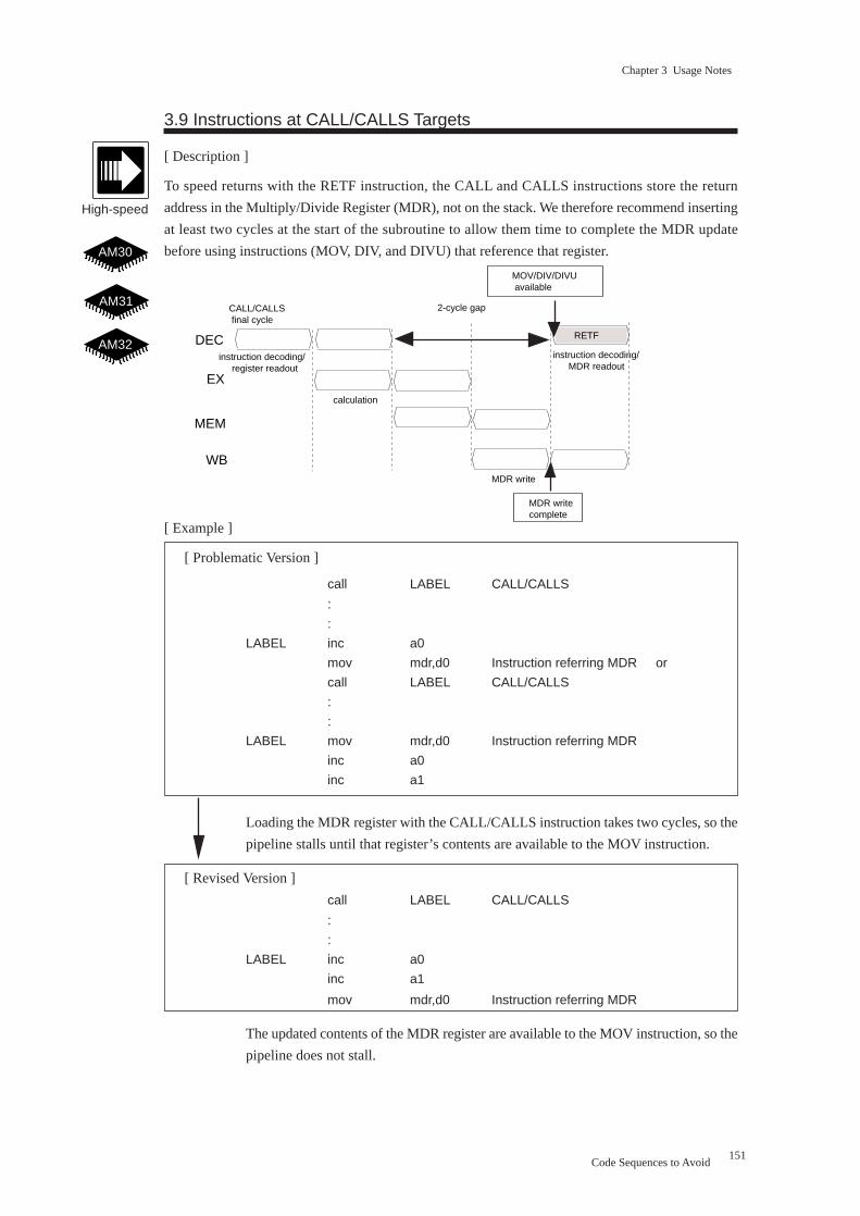
151
Chapter 3 Usage Notes
3.9 Instructions at CALL/CALLS Targets
[ Description ]
To speed returns with the RETF instruction, the CALL and CALLS instructions store the return
address in the Multiply/Divide Register (MDR), not on the stack. We therefore recommend inserting
at least two cycles at the start of the subroutine to allow them time to complete the MDR update
before using instructions (MOV, DIV, and DIVU) that reference that register.
[ Example ]
[ Problematic Version ]
call LABEL CALL/CALLS
:
:
LABEL inc a0
mov mdr,d0 Instruction referring MDR or
call LABEL CALL/CALLS
:
:
LABEL mov mdr,d0 Instruction referring MDR
inc a0
inc a1
Loading the MDR register with the CALL/CALLS instruction takes two cycles, so the
pipeline stalls until that register’s contents are available to the MOV instruction.
[ Revised Version ]
call LABEL CALL/CALLS
:
:
LABEL inc a0
inc a1
mov mdr,d0 Instruction referring MDR
The updated contents of the MDR register are available to the MOV instruction, so the
pipeline does not stall.
Code Sequences to Avoid
calculation
DEC
MEM
EX
WB
instruction decoding/ register readout
RETF
2-cycle gap
MDR writecomplete
CALL/CALLS final cycle
MDR write
instruction decoding/ MDR readout
MOV/DIV/DIVU available
AM31
AM30
AM32
High-speed
152
Chapter 3 Usage Notes
Code Sequences to Avoid
[ Applicable Instructions ]
<Leading instruction> CALL or CALLS
<Following instruction> MOV MDR, Dn, DIV, DIVU
The above coding examples omit the FUNCINFO directives required with each CALL
instruction. For a detailed description of FUNCINFO syntax, refer to the Cross Assembler
User’s Manual.
Chapter 3 Usage Notes
153
Boiler Plate Code Sequences
4.1 Reset Routine
[ Description ]
A reset start leaves all registers with indeterminate contents, so always start by initiating registers.
The Stack Pointer (SP) is particularly important.
If the user application program uses level interrupts, initialize the interrupt vector registers as well.
[ Example ]
IVAR0 equ 0x20000000
IVAR1 equ 0x20000004
IVAR2 equ 0x20000008
IVAR3 equ 0x2000000c
IVAR4 equ 0x20000010
IVAR5 equ 0x20000014
IVAR6 equ 0x20000018
;
Reset routine
;
org 0x40000000 ; Entry point for reset
RESET:
jmp STARTUP
org 0x40000008 ; Entry point for nonmaskable interrupt
NMIROUTINE:
....
STARTUP:
mov STCKTP,a0 ; Initialize Stack Pointer(SP) to word boundary
; (divisible by 4)
mov a0,sp
clr d0 ; Clear all registers
mov d0,d1
mov d0,d2
mov d0,d3
mov d0,a0
mov d0,a0
mov a0,a1
mov a0,a2
mov a0,a3
mov IRQ0ROUTINE,a0 ; Set to lower 16 bits of entry point for level interrupt
handler
movhu a0,(IVATo)
mov IRQ1ROUTINE,a0
movhu a0,(IVAR1)
mov IRQ2ROUTINE,a0
movhu a0,a0,(IVAR2)
4Boiler plate
Boiler Plate Code Sequences
Chapter 3 Usage Notes
154
mov IRQ3ROUTINE,a0
movhu a0,(IVAR3)
mov IRQ4ROUTINE,a0
movhu a0,(IVAR4)
mov IRQ5ROUTINE,a0
movhu a0,(IVAR5)
mov IRQ6ROUTINE,a0
movhu a0,(IVAR6)
4.2 Interrupt Handlers
[ Description ]
There are two types of interrupt handlers: for nonmaskable interrupts and for level interrupts.
For level interrupts, the Interrupt Group Register (IAGR) gives the group number. Assigning only
one interrupt source to an interrupt level speeds response by eliminating the need for differentiation
logic.
With store buffer models, always ensure clearing of the interrupt source by separating the write to the
interrupt control register and the RTI instruction--with a vacuous read of that register, for example.
For the serial debugger's special requirements for the nonmaskable interrupt handler, refer to the
MN10300 Series C Source Code Debugger User's Manual.
[ Example ]
;
Interrupt handler for NMI, level 0 interrupts and level 1 interrupts
;
IAGR equ 0x34000200
IVAR0 equ 0x20000000
IVAR1 equ 0x20000004
IVAR2 equ 0x20000008
IVAR3 equ 0x2000000c
IVAR4 equ 0x20000010
IVAR5 equ 0x20000014
IVAR6 equ 0x20000018
G01CR equ 0x34000100
G31CR equ 0x3400010c
;
Nonmaskable interrupt handler
;
org 0x40000008 ; Entry point for nonmaskable interrupts
NMIROUTINE:
add -8,sp
mov a0,(4,sp) ; Save registers used by handler
mov d0,(sp)
mov G01CR,a0
mov (ao),d0 ; Get NMI source
Boiler plate
Boiler Plate Code Sequences
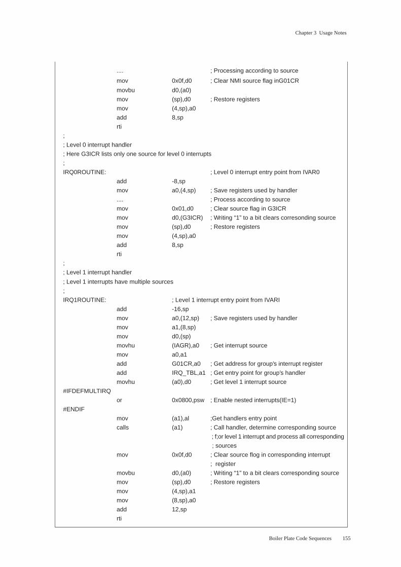
Chapter 3 Usage Notes
155
.... ; Processing according to source
mov 0x0f,d0 ; Clear NMI source flag inG01CR
movbu d0,(a0)
mov (sp),d0 ; Restore registers
mov (4,sp),a0
add 8,sp
rti
;
; Level 0 interrupt handler
; Here G3ICR lists only one source for level 0 interrupts
;
IRQ0ROUTINE: ; Level 0 interrupt entry point from IVAR0
add -8,sp
mov a0,(4,sp) ; Save registers used by handler
.... ; Process according to source
mov 0x01,d0 ; Clear source flag in G3ICR
mov d0,(G3ICR) ; Writing “1” to a bit clears corresonding source
mov (sp),d0 ; Restore registers
mov (4,sp),a0
add 8,sp
rti
;
; Level 1 interrupt handler
; Level 1 interrupts have multiple sources
;
IRQ1ROUTINE: ; Level 1 interrupt entry point from IVARI
add -16,sp
mov a0,(12,sp) ; Save registers used by handler
mov a1,(8,sp)
mov d0,(sp)
movhu (IAGR),a0 ; Get interrupt source
mov a0,a1
add G01CR,a0 ; Get address for group’s interrupt register
add IRQ_TBL,a1 ; Get entry point for group’s handler
movhu (a0),d0 ; Get level 1 interrupt source
#IFDEFMULTIRQ
or 0x0800,psw ; Enable nested interrupts(IE=1)
#ENDIF
mov (a1),al ;Get handlers entry point
calls (a1) ; Call handler, determine corresponding source
; f;or level 1 interrupt and process all corresponding
; sources
mov 0x0f,d0 ; Clear source flog in corresponding interrupt
; register
movbu d0,(a0) ; Writing “1” to a bit clears corresponding source
mov (sp),d0 ; Restore registers
mov (4,sp),a1
mov (8,sp),a0
add 12,sp
rti
Boiler Plate Code Sequences
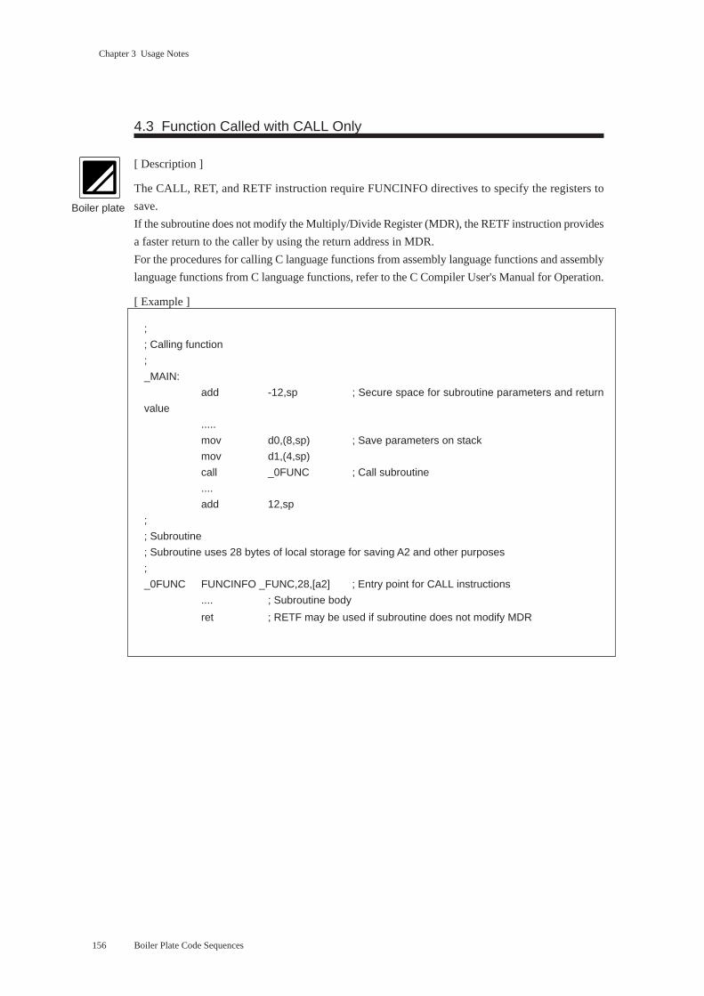
Chapter 3 Usage Notes
156
4.3 Function Called with CALL Only
[ Description ]
The CALL, RET, and RETF instruction require FUNCINFO directives to specify the registers to
save.
If the subroutine does not modify the Multiply/Divide Register (MDR), the RETF instruction provides
a faster return to the caller by using the return address in MDR.
For the procedures for calling C language functions from assembly language functions and assembly
language functions from C language functions, refer to the C Compiler User's Manual for Operation.
[ Example ]
;
; Calling function
;
_MAIN:
add -12,sp ; Secure space for subroutine parameters and return
value
.....
mov d0,(8,sp) ; Save parameters on stack
mov d1,(4,sp)
call _0FUNC ; Call subroutine
....
add 12,sp
;
; Subroutine
; Subroutine uses 28 bytes of local storage for saving A2 and other purposes
;
_0FUNC FUNCINFO _FUNC,28,[a2] ; Entry point for CALL instructions
.... ; Subroutine body
ret ; RETF may be used if subroutine does not modify MDR
Boiler plate
Boiler Plate Code Sequences
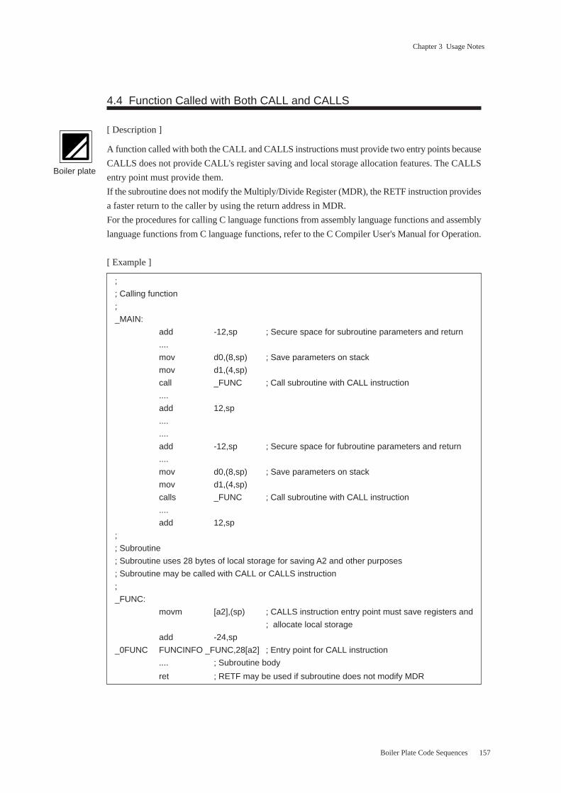
Chapter 3 Usage Notes
157
4.4 Function Called with Both CALL and CALLS
[ Description ]
A function called with both the CALL and CALLS instructions must provide two entry points because
CALLS does not provide CALL's register saving and local storage allocation features. The CALLS
entry point must provide them.
If the subroutine does not modify the Multiply/Divide Register (MDR), the RETF instruction provides
a faster return to the caller by using the return address in MDR.
For the procedures for calling C language functions from assembly language functions and assembly
language functions from C language functions, refer to the C Compiler User's Manual for Operation.
[ Example ]
;
; Calling function
;
_MAIN:
add -12,sp ; Secure space for subroutine parameters and return
....
mov d0,(8,sp) ; Save parameters on stack
mov d1,(4,sp)
call _FUNC ; Call subroutine with CALL instruction
....
add 12,sp
....
....
add -12,sp ; Secure space for fubroutine parameters and return
....
mov d0,(8,sp) ; Save parameters on stack
mov d1,(4,sp)
calls _FUNC ; Call subroutine with CALL instruction
....
add 12,sp
;
; Subroutine
; Subroutine uses 28 bytes of local storage for saving A2 and other purposes
; Subroutine may be called with CALL or CALLS instruction
;
_FUNC:
movm [a2],(sp) ; CALLS instruction entry point must save registers and
; allocate local storage
add -24,sp
_0FUNC FUNCINFO _FUNC,28[a2] ; Entry point for CALL instruction
.... ; Subroutine body
ret ; RETF may be used if subroutine does not modify MDR
Boiler plate
Boiler Plate Code Sequences

Chapter 3 Usage Notes
158
4Appendix
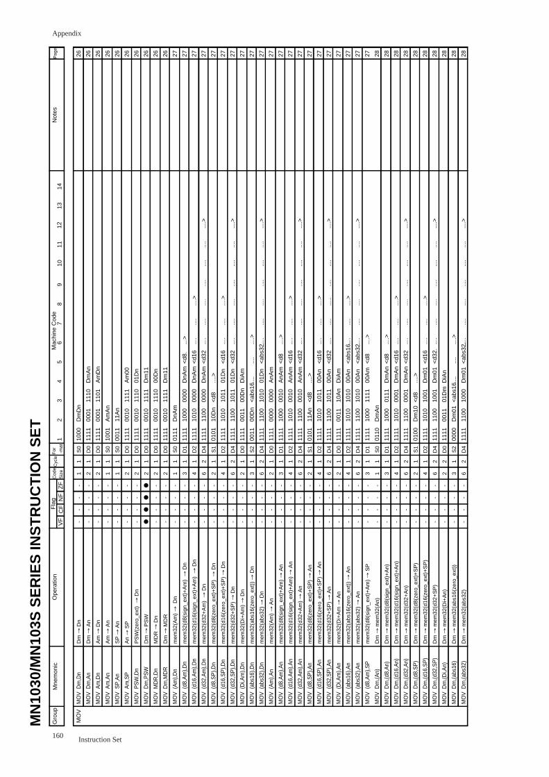
Appendix
160 Instruction Set
MO
V D
m,D
n�
MO
V D
m,A
n�
MO
V A
m,D
n�
MO
V A
m,A
n�
MO
V S
P,A
n�
MO
V A
m,S
P �
MO
V P
SW
,Dn�
MO
V D
m,P
SW
�
MO
V M
DR
,Dn�
MO
V D
m,M
DR
�
MO
V (
Am
),Dn�
MO
V (
d8,A
m),D
n�
MO
V (
d16,
Am
),Dn�
MO
V (
d32,
Am
),Dn�
MO
V (
d8,S
P),D
n�
MO
V (
d16,
SP
),Dn�
MO
V (
d32,
SP
),Dn�
MO
V (
Di,A
m),D
n�
MO
V (
abs1
6),D
n�
MO
V (
abs3
2),D
n�
MO
V (
Am
),An�
MO
V (
d8,A
m),A
n�
MO
V (
d16,
Am
),An�
MO
V (
d32,
Am
),An�
MO
V (
d8,S
P),A
n�
MO
V (
d16,
SP
),An�
MO
V (
d32,
SP
),An�
MO
V (
Di,A
m),A
n�
MO
V (
abs1
6),A
n�
MO
V (
abs3
2),A
n�
MO
V (
d8,A
m),S
P�
MO
V D
m,(A
n)�
MO
V D
m,(d
8,A
n)�
MO
V D
m,(d
16,A
n)�
MO
V D
m,(d
32,A
n)�
MO
V D
m,(d
8,S
P)�
MO
V D
m,(d
16,S
P)�
MO
V D
m,(d
32,S
P)�
MO
V D
m,(D
i,An)
�
MO
V D
m,(a
bs16
)�
MO
V D
m,(a
bs32
)�
�
Dm
→ D
n�
Dm
→ A
n�
Am
→ D
n�
Am
→ A
n�
SP
→ A
n�
An →
SP
�
PS
W(z
ero_
ext)
→ D
n�
Dm
→ P
SW
�
MD
R →
Dn�
Dm
→ M
DR
�
mem
32(A
m) →
Dn�
mem
32(d
8(si
gn_e
xt)+
Am
) →
Dn�
mem
32(d
16(s
ign_
ext)
+A
m)
→ D
n�
mem
32(d
32+
Am
) →
Dn�
mem
32(d
8(ze
ro_e
xt)+
SP
) →
Dn�
mem
32(d
16(z
ero_
ext)
+S
P) →
Dn�
mem
32(d
32+
SP
) →
Dn�
mem
32(D
i+A
m) →
Dn�
mem
32(a
bs16
(zer
o_ex
t)) →
Dn�
mem
32(a
bs32
) →
Dn�
mem
32(A
m) →
An�
mem
32(d
8(si
gn_e
xt)+
Am
) →
An�
mem
32(d
16(s
ign_
ext)
+A
m) →
An�
mem
32(d
32+
Am
) →
An�
mem
32(d
8(ze
ro_e
xt)+
SP
) →
An�
mem
32(d
16(z
ero_
ext)
+S
P) →
An�
mem
32(d
32+
SP
) →
An�
mem
32(D
i+A
m →
An�
mem
32(a
bs16
(zer
o_ex
t)) →
An�
mem
32(a
bs32
) →
An�
mem
32(d
8(si
gn_e
xt)+
Am
) →
SP
�
Dm
→ m
em32
(An)
�
Dm
→ m
em32
(d8(
sign
_ext
)+A
n)�
Dm
→ m
em32
(d16
(sig
n_ex
t)+
An)
�
Dm
→ m
em32
(d32
+A
n)�
Dm
→ m
em32
(d8(
zero
_ext
)+S
P)�
Dm
→ m
em32
(d16
(zer
o_ex
t)+
SP
)�
Dm
→ m
em32
(d32
+S
P)�
Dm
→ m
em32
(Di+
An)
�
Dm
→ m
em32
(abs
16(z
ero_
ext)
)�
Dm
→ m
em32
(abs
32)�
� �
-� -� -� -� -� -� -� ●� -� -� -� -� -� -� -� -� -� -� -� -� -� -� -� -� -� -� -� -� -� -� -� -� -� -� -� -� -� -� -� -� -� � �
-� -� -� -� -� -� -� ●� -� -� -� -� -� -� -� -� -� -� -� -� -� -� -� -� -� -� -� -� -� -� -� -� -� -� -� -� -� -� -� -� -� �
-� -� -� -� -� -� -� ●� -� -� -� -� -� -� -� -� -� -� -� -� -� -� -� -� -� -� -� -� -� -� -� -� -� -� -� -� -� -� -� -� -� �
-� -� -� -� -� -� -� ●� -� -� -� -� -� -� -� -� -� -� -� -� -� -� -� -� -� -� -� -� -� -� -� -� -� -� -� -� -� -� -� -� -� �
1� 2� 2� 1� 1� 2� 2� 2� 2� 2� 1� 3� 4� 6� 2� 4� 6� 2� 3� 6� 2� 3� 4� 6� 2� 4� 6� 2� 4� 6� 3� 1� 3� 4� 6� 2� 4� 6� 2� 3� 6
1� 1� 1� 1� 1� 1� 1� 1� 1� 1� 1� 1� 1� 2� 1� 1� 2� 1� 1� 2� 1� 1� 1� 2� 1� 1� 2� 1� 1� 2� 1� 1� 1� 1� 2� 1� 1� 2� 2� 1� 2
S0�
D0�
D0�
S0�
S0�
D0�
D0�
D0�
D0�
D0�
S0�
D1�
D2�
D4�
S1�
D2�
D4�
D0�
S2�
D4�
D0�
D1�
D2�
D4�
S1�
D2�
D4�
D0�
D2�
D4�
D1�
S0�
D1�
D2�
D4�
S1�
D2�
D4�
D0�
S2�
D4� �
1� � 1000
�
1111
�
1111
�
1001
�
0011
�
1111
�
1111
�
1111
�
1111
�
1111
�
0111
�
1111
�
1111
�
1111
�
0101
�
1111
�
1111
�
1111
�
0011
�
1111
�
1111
�
1111
�
1111
�
1111
�
0101
�
1111
�
1111
�
1111
�
1111
�
1111
�
1111
�
0110
�
1111
�
1111
�
1111
�
0100
�
1111
�
1111
�
1111
�
0000
�
1111
�
�
2� � Dm
Dn�
0001
�
0001
�
Am
An�
11A
n�
0010
�
0010
�
0010
�
0010
�
0010
�
DnA
m�
1000
�
1010
�
1100
�
10D
n�
1010
�
1100
�
0011
�
00D
n�
1100
�
0000
�
1000
�
1010
�
1100
�
11A
n�
1010
�
1100
�
0011
�
1010
�
1100
�
1000
�
Dm
An�
1000
�
1010
�
1100
�
Dm
10�
1010
�
1100
�
0011
�
Dm
01�
1100
�
�
3� � � 1110
�
1101
�
� � 1111
�
1110
�
1111
�
1110
�
1111
�
� 0000
�
0000
�
0000
�
<d8
�
1011
�
1011
�
00D
n�
<ab
s16�
1010
�
0000
�
0010
�
0010
�
0010
�
<d8
�
1011
�
1011
�
10A
n�
1010
�
1010
�
1111
�
� 0111
�
0001
�
0001
�
<d8
�
1001
�
1001
�
01D
m�
<ab
s16�
1000
�
�
4� � � Dm
An�
Am
Dn�
� � Am
00�
01D
n�
Dm
11�
00D
n�
Dm
11�
� DnA
m�
DnA
m�
DnA
m�
....>
�
01D
n�
01D
n�
DiA
m�
....�
01D
n�
AnA
m�
AnA
m�
AnA
m�
AnA
m�
....>
�
00A
n�
00A
n�
DiA
m�
00A
n�
00A
n�
00A
m�
� Dm
An�
Dm
An�
Dm
An�
....>
�
Dm
01�
Dm
01�
DiA
n�
....�
Dm
01�
�
5� � � � � � � � � � � � � <d8
.�
<d1
6�
<d3
2�
� <d1
6�
<d3
2�
� ....�
<ab
s32�
� <d8
�
<d1
6�
<d3
2�
� <d1
6�
<d3
2�
� <ab
s16�
<ab
s32�
<d8
�
� <d8
�
<d1
6�
<d3
2�
� <d1
6�
<d3
2.�
� ....�
<ab
s32.
�
�
6� � � � � � � � � � � � � ...>
�
....�
....�
� ....�
....�
� ....>
�
....�
� ....>
�
....�
....�
� ....�
....�
� ....�
....�
....>
�
� ....>
�
....�
....�
� ....�
....�
� ....>
�
....�
�
Gro
up�
�
Mne
mon
icO
pera
tion
Mac
hine
Cod
eN
otes
Pag
e�
� �
Fla
gC
ode�
Siz
eC
ycle
For
�
-m
at
MN
1030
/MN
103S
SE
RIE
S IN
ST
RU
CT
ION
SE
T7� � � � � � � � � � � � � � ...
.�
....�
� ....�
....�
� � ....�
� � ....�
....�
� ....�
....�
� ....�
....�
� � � ....�
....�
� ....�
....�
� � ....�
�
8� � � � � � � � � � � � � � ....>
�
....�
� ....>
�
....�
� � ....�
� � ....>
�
....�
� ....>
�
.....�
� ....>
�
....�
� � � ....>
�
....�
� ....>
�
....�
� � ....�
�
9� � � � � � � � � � � � � � � ....�
� � ....�
� � ....�
� � � ....�
� � ....�
� � ....�
� � � � ....�
� � ....�
� � ....�
�
10�
� � � � � � � � � � � � � � ....�
� � ....�
� � ....�
� � � ....�
� � ....�
� � ....�
� � � � ....�
� � ....�
� � ....�
�
11�
� � � � � � � � � � � � � � ....�
� � ....�
� � ....�
� � � ....�
� � ....�
� � ....�
� � � � ....�
� � ....�
� � ....�
�
12�
� � � � � � � � � � � � � � ....>
�
� � ....>
�
� � ....>
�
� � � ....>
�
� � ....>
�
� � ....>
�
� � � � ....>
�
� � ....>
�
� � ....>
�
�
1314
MO
V
VF
CF
NF
ZF
26�
26�
26�
26�
26�
26�
26�
26�
26�
26�
27�
27�
27�
27�
27�
27�
27�
27�
27�
27�
27�
27�
27�
27�
27�
27�
27�
27�
27�
27�
27�
28�
28�
28�
28�
28�
28�
28�
28�
28�
28
�
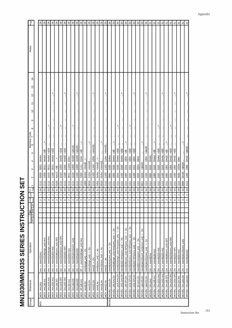
Appendix
161Instruction Set
MO
V A
m,(
An)
�
MO
V A
m,(
d8,A
n)�
MO
V A
m,(
d16,
An)
�
MO
V A
m,(
d32,
An)
�
MO
V A
m,(
d8,S
P)�
MO
V A
m,(
d16,
SP
)�
MO
V A
m,(
d32,
SP
)�
MO
V A
m,(
Di,A
n)�
MO
V A
m,(
abs1
6)�
MO
V A
m,(
abs3
2)�
MO
V S
P,(
d8,A
n)�
MO
V i
mm
8,D
n�
MO
V i
mm
16,D
n�
MO
V i
mm
32,D
n�
MO
V i
mm
8,A
n�
MO
V i
mm
16,A
n�
MO
V i
mm
32,A
n�
MO
VB
U (
Am
),D
n�
MO
VB
U (
d8,A
m),
Dn�
MO
VB
U (
d16,
Am
),D
n�
MO
VB
U (
d32,
Am
),D
n�
MO
VB
U (
d8,S
P),
Dn�
MO
VB
U (
d16,
SP
),D
n�
MO
VB
U (
d32,
SP
),D
n�
MO
VB
U (
Di,A
m),
Dn�
MO
VB
U (
abs1
6),D
n�
MO
VB
U (
abs3
2),D
n�
MO
VB
U D
m,(
An)
�
MO
VB
U D
m,(
d8,A
n)�
MO
VB
U D
m,(
d16,
An)
�
MO
VB
U D
m,(
d32,
An)
�
MO
VB
U D
m,(
d8,S
P)�
MO
VB
U D
m,(
d16,
SP
)�
MO
VB
U D
m,(
d32,
SP
)�
MO
VB
U D
m,(
Di,A
n)�
MO
VB
U D
m,(
abs1
6)�
MO
VB
U D
m,(
abs3
2)�
� � �
Am
→ m
em32
(An)
�
Am
→ m
em32
(d8(
sign
_ext
)+A
n)�
Am
→ m
em32
(d16
(sig
n_ex
t)+
An)
�
Am
→ m
em32
(d32
+A
n)�
Am
→ m
em32
(d8(
zero
_ext
)+S
P)�
Am
→ m
em32
(d16
(zer
o_ex
t)+
SP
)�
Am
→ m
em32
(d32
+S
P)�
Am
→ m
em32
(Di+
An)
�
Am
→ m
em32
(abs
16(z
ero_
ext)
)�
Am
→ m
em32
(abs
32)�
SP
→ m
em32
(d8(
sign
_ext
)+A
n)�
imm
8(si
gn_e
xt) →
Dn�
imm
16(s
ign_
ext)
→ D
n�
imm
32 →
Dn�
imm
8(ze
ro_e
xt] →
An�
imm
16(z
ero_
ext)
→ A
n�
imm
32 →
An�
mem
8(A
m)(
zero
_ext
) →
Dn�
mem
8(d8
(sig
n_ex
t)+
Am
)(ze
ro_e
xt) →
Dn�
mem
8(d1
6(si
gn_e
xt)+
Am
)(ze
ro_e
xt)
→ D
n �
mem
8(d3
2+A
m)(
zero
_ext
] → D
n�
mem
8(d8
(zer
o_ex
t)+
SP
)(ze
ro_e
xt)
→ D
n�
mem
8(d1
6(ze
ro_e
xt)+
SP
)(ze
ro_e
xt)
→ D
n�
mem
8(d3
2+S
P)(
zero
_ext
) →
D
n�
mem
8(D
i+A
m)(
zero
_ext
) →
Dn�
mem
8(ab
s16(
zero
_ext
))(z
ero_
ext] →
D
n�
mem
8(ab
s32)
(zer
o_ex
t) →
Dn�
Dm
→ m
em8(
An)
�
Dm
→ m
em8(
d8+
An)
�
Dm
→ m
em8(
d16+
An)
�
Dm
→ m
em8(
d32+
An)
�
Dm
→ m
em8(
d8(z
ero_
ext)
+S
P)�
Dm
→ m
em8(
d16(
zero
_ext
)+S
P)�
Dm
→ m
em8(
d32+
SP
)�
Dm
→ m
em8(
Di+
An)
�
Dm
→ m
em8(
abs1
6(ze
ro_e
xt))
�
Dm
→ m
em8(
abs3
2)�
� � � � � � � � �
-� -� -� -� -� -� -� -� -� -� -� -� -� -� -� -� -� -� -� -� -� -� -� -� -� -� -� -� -� -� -� -� -� -� -� -� -
-� -� -� -� -� -� -� -� -� -� -� -� -� -� -� -� -� -� -� -� -� -� -� -� -� -� -� -� -� -� -� -� -� -� -� -� -
-� -� -� -� -� -� -� -� -� -� -� -� -� -� -� -� -� -� -� -� -� -� -� -� -� -� -� -� -� -� -� -� -� -� -� -� -
-� -� -� -� -� -� -� -� -� -� -� -� -� -� -� -� -� -� -� -� -� -� -� -� -� -� -� -� -� -� -� -� -� -� -� -� -
2� 3� 4� 6� 2� 4� 6� 2� 4� 6� 3� 2� 3� 6� 2� 3� 6� 2� 3� 4� 6� 3� 4� 6� 2� 3� 6� 2� 3� 4� 6� 3� 4� 6� 2� 3� 6
1� 1� 1� 2� 1� 1� 2� 2� 1� 2� 1� 1� 1� 2� 1� 1� 2� 1� 1� 1� 2� 1� 1� 2� 1� 1� 2� 1� 1� 1� 2� 1� 1� 2� 2� 1� 2
D0�
D1�
D2�
D4�
S1�
D2�
D4�
D0�
D2�
D4�
D1�
S1�
S2�
D4�
S1�
S2�
D4�
D0�
D1�
D2�
D4�
D1�
D2�
D4�
D0�
S2�
D4�
D0�
D1�
D2�
D4�
D1�
D2�
D4�
D0�
S2�
D4� �
1� � 1111
�
1111
�
1111
�
1111
�
0100
�
1111
�
1111
�
1111
�
1111
�
1111
�
1111
�
1000
�
0010
�
1111
�
1001
�
0010
�
1111
�
1111
�
1111
�
1111
�
1111
�
1111
�
1111
�
1111
�
1111
�
0011
�
1111
�
1111
�
1111
�
1111
�
1111
�
1111
�
1111
�
1111
�
1111
�
0000
�
1111
�
� �
2� � 0000
�
1000
�
1010
�
1100
�
Am
11�
1010
�
1100
�
0011
�
1010
�
1100
�
1000
�
DnD
n�
11D
n�
1100
�
AnA
n�
01A
n�
1100
�
0000
�
1000
�
1010
�
1100
�
1000
�
1010
�
1100
�
0100
�
01D
n�
1100
�
0000
�
1000
�
1010
�
1100
�
1000
�
1010
�
1100
�
0100
�
Dm
10�
1100
�
�
3� � 0001
�
0011
�
0011
�
0011
�
<d8
�
1001
�
1001
�
11A
m�
1000
�
1000
�
1111
�
<im
m8�
<im
m16
�
1100
�
<im
m8�
<im
m16
�
1101
�
0100
�
0100
�
0100
�
0100
�
1011
�
1011
�
1011
�
00D
n�
<abs
16�
1010
�
0101
�
0101
�
0101
�
0101
�
1001
�
1001
�
1001
�
01D
m�
<abs
16�
1000
�
� � � �
4� � Am
An�
Am
An�
Am
An�
Am
An�
....>
�
Am
00�
Am
00�
DiA
n�
Am
00�
Am
00�
01A
n�
...>
�
....
�
10D
n�
....>
�
....�
11A
n�
DnA
m�
DnA
m�
DnA
m�
DnA
m�
10D
n�
10D
n�
10D
n�
DiA
m�
....�
10D
n�
Dm
An�
Dm
An�
Dm
An�
Dm
An�
Dm
10�
Dm
10�
Dm
10�
DiA
n�
....�
Dm
10�
�
5� � � <d8
�
<d1
6�
<d3
2�
� <d1
6�
<d3
2�
� <ab
s16�
<ab
s32�
<d8
�
� ....�
<im
m32
�
� ....�
<im
m32
�
� <d8�
<d16
�
<d32
�
<d8�
<d16
�
<d32
�
� ....�
<abs
32�
� <d8�
<d16
�
<d32
�
<d8�
<d16
�
<d32
�
� ....�
<abs
32�
� �
6� � � ....>
�
....�
....�
� ....�
....�
� ....�
....�
....>
�
� ....>
�
....�
� ....>
�
....�
� ....>
�
....�
....�
....>
�
....�
....�
� ....>
�
....�
� ....>
�
....�
....�
....>
�
....�
....�
� ....>
�
....
� �
Gro
up�
�
Mne
mon
icO
pera
tion
Mac
hine
Cod
eN
otes
Pag
eF
lag
Cod
e�
Siz
eC
ycle
For
�
-m
at
MN
1030
/MN
103S
SE
RIE
S IN
ST
RU
CT
ION
SE
T7� � � � ...
.�
....�
� ....�
....�
� ....�
....�
� � � ....�
� � ....�
� � ....�
....�
� ....�
....�
� � ....�
� � ....�
....�
� ....�
....�
� � ....
8� � � � ....>
�
....�
� ....>
�
....�
� ....>
�
....�
� � � ....�
� � ....�
� � ....>
�
....�
� ....>
�
....�
� � ....�
� � ....>
�
....�
� ....>
�
....�
� � ....
9� � � � � ....�
� � ....�
� � ....�
� � � ....�
� � ....�
� � � ....�
� � ....�
� � ....�
� � � ....�
� � ....�
� � ....
10�
� � � � ....�
� � ....�
� � ....�
� � � ....�
� � ....�
� � � ....�
� � ....�
� � ....�
� � � ....�
� � ....�
� � ....
11�
� � � � ....�
� � ....�
� � ....�
� � � ....�
� � ....�
� � � ....�
� � ....�
� � ....�
� � � ....�
� � ....�
� � ....
12�
� � � � ....>
�
� � ....>
�
� � ....>
�
� � � ....>
�
� � ....>
�
� � � ....>
�
� � ....>
�
� � ....>
�
� � � ....>
�
� � ....>
�
� � ....>
1314
VF
CF
NF
ZF
MO
V�
� � � � � � � � � � � � � � � � MO
VB
U
28�
28�
28�
28�
28�
28�
28�
28�
28�
28�
28�
29�
29�
29�
29�
29�
29�
30�
30�
30�
30�
30�
30�
30�
30�
30�
30�
31�
31�
31�
31�
31�
31�
31�
31�
31�
31� �
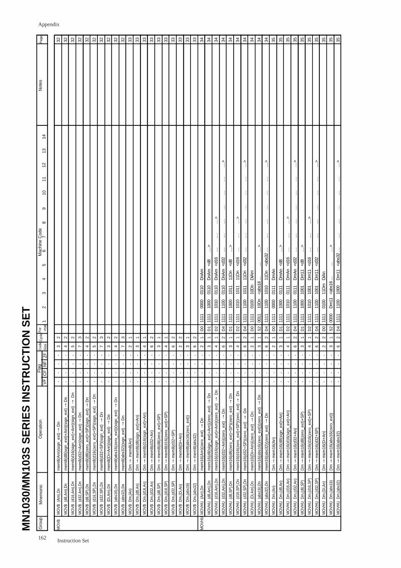
Appendix
162 Instruction Set
MO
VB
(A
m),D
n�
MO
VB
(d8
,Am
),Dn�
MO
VB
(d1
6,A
m),D
n�
MO
VB
(d3
2,A
m),D
n�
MO
VB
(d8
,SP
),Dn�
MO
VB
(d1
6,S
P),D
n�
MO
VB
(d3
2,S
P),D
n�
MO
VB
(D
i,Am
),Dn�
MO
VB
(ab
s16)
,Dn�
MO
VB
(ab
s32)
,Dn�
MO
VB
Dm
,(An)
�
MO
VB
Dm
,(d8,
An)
�
MO
VB
Dm
,(d16
,An)
�
MO
VB
Dm
,(d32
,An)
�
MO
VB
Dm
,(d8,
SP
)�
MO
VB
Dm
,(d16
,SP
)�
MO
VB
Dm
,(d32
,SP
)�
MO
VB
Dm
,(Di,A
n)�
MO
VB
Dm
,(abs
16)�
MO
VB
Dm
,(abs
32)�
MO
VH
U (
Am
),Dn�
MO
VH
U (
d8,A
m),D
n�
MO
VH
U (
d16,
Am
),Dn�
MO
VH
U (
d32,
Am
),Dn�
MO
VH
U (
d8,S
P),D
n�
MO
VH
U (
d16,
SP
),Dn�
MO
VH
U (
d32,
SP
),Dn�
MO
VH
U (
Di,A
m),D
n�
MO
VH
U (
abs1
6),D
n�
MO
VH
U (
abs3
2),D
n�
MO
VH
U D
m,(A
n)�
MO
VH
U D
m,(d
8,A
n)�
MO
VH
U D
m,(d
16,A
n)�
MO
VH
U D
m,(d
32,A
n)�
MO
VH
U D
m,(d
8,S
P)�
MO
VH
U D
m,(d
16,S
P)�
MO
VH
U D
m,(d
32,S
P)�
MO
VH
U D
m,(D
i,An)
�
MO
VH
U D
m,(a
bs16
)�
MO
VH
U D
m,(a
bs32
)
mem
8(A
m)(
sign
_ext
) →
Dn�
mem
8(d8
(sig
n_ex
t)+A
m)(
sign
_ext
) →
Dn�
mem
8(d1
6(si
gn_e
xt)+
Am
)(si
gn_e
xt)
→ D
n�
mem
8(d3
2+A
m)(
sign
_ext
) →
Dn�
mem
8(d8
(zer
o_ex
t)+S
P)(
sign
_ext
) →
Dn�
mem
8(d1
6(ze
ro_e
xt)+
SP
)(si
gn_e
xt)
→ D
n�
mem
8(d3
2+S
P)(
sign
_ext
) →
Dn�
mem
8(D
i+A
m)(
sign
_ext
) →
Dn�
mem
8(ab
s16(
zero
_ext
))(s
ign_
ext)
→ D
n�
mem
8(ab
s32)
(sig
n_ex
t) →
Dn�
Dm
→ m
em8(
An)
�
Dm
→ m
em8(
d8(s
ign_
ext)
+An)
�
Dm
→ m
em8(
d16(
sign
_ext
)+A
n)�
Dm
→ m
em8(
d32+
An)
�
Dm
→ m
em8(
d8(z
ero_
ext)
+SP
)�
Dm
→ m
em8(
d16(
zero
_ext
)+S
P)�
Dm
→ m
em8(
d32+
SP
)�
Dm
→ m
em8(
Di+
An)
�
Dm
→ m
em8(
abs1
6(ze
ro_e
xt))
�
Dm
→ m
em8(
abs3
2)�
mem
16(A
m)(
zero
_ext
) →
Dn�
mem
16(d
8(si
gn_e
xt)+
Am
)(ze
ro_e
xt)
→ D
n�
mem
16(d
16(s
ign_
ext)
+Am
)(ze
ro_e
xt)
→ D
n�
mem
16(d
32+A
m)(
zero
_ext
) →
Dn�
mem
16(d
8(ze
ro_e
xt)+
SP
)(ze
ro_e
xt)
→ D
n�
mem
16(d
16(z
ero_
ext)
+SP
)(ze
ro_e
xt) →
Dn�
mem
16(d
32+S
P)(
zero
_ext
) →
Dn�
mem
16(D
i+A
m)(
zero
_ext
) →
Dn�
mem
16(a
bs16
(zer
o_ex
t))(
zero
_ext
) →
Dn�
mem
16(a
bs32
)(ze
ro_e
xt)
→ D
n�
Dm
→ m
em16
(An)
�
Dm
→ m
em16
(d8(
sign
_ext
)+A
n)�
Dm
→ m
em16
(d16
(sig
n_ex
t)+A
n)�
Dm
→ m
em16
(d32
+An)
�
Dm
→ m
em16
(d8(
zero
_ext
)+S
P)�
Dm
→ m
em16
(d16
(zer
o_ex
t)+S
P)�
Dm
→ m
em16
(d32
+SP
)�
Dm
→ m
em16
(Di+
An)
�
Dm
→ m
em16
(abs
16(z
ero_
ext)
)�
Dm
→ m
em16
(abs
32)
-� -� -� -� -� -� -� -� -� -� -� -� -� -� -� -� -� -� -� -� -� -� -� -� -� -� -� -� -� -� -� -� -� -� -� -� -� -� -� -� � �
-� -� -� -� -� -� -� -� -� -� -� -� -� -� -� -� -� -� -� -� -� -� -� -� -� -� -� -� -� -� -� -� -� -� -� -� -� -� -� -� �
-� -� -� -� -� -� -� -� -� -� -� -� -� -� -� -� -� -� -� -� -� -� -� -� -� -� -� -� -� -� -� -� -� -� -� -� -� -� -� -
-� -� -� -� -� -� -� -� -� -� -� -� -� -� -� -� -� -� -� -� -� -� -� -� -� -� -� -� -� -� -� -� -� -� -� -� -� -� -� -� � �
3� 4� 5� 7� 4� 5� 7� 3� 4� 7� 2� 3� 4� 6� 3� 4� 6� 2� 3� 6� 2� 3� 4� 6� 3� 4� 6� 2� 3� 6� 2� 3� 4� 6� 3� 4� 6� 2� 3� 6
2� 2� 2� 3� 2� 2� 3� 2� 2� 3� 1� 1� 1� 2� 1� 1� 2� 2� 1� 2� 1� 1� 1� 2� 1� 1� 2� 1� 1� 2� 1� 1� 1� 2� 1� 1� 2� 2� 1� 2
� � � � � � � � � � � � � � � � � � � �
D0�
D1�
D2�
D4�
D1�
D2�
D4�
D0�
S2�
D4�
D0�
D1�
D2�
D4�
D1�
D2�
D4�
D0�
S2�
D4
1� � � � � � � � � � � � � � � � � � � � � � 1111
�
1111
�
1111
�
1111
�
1111
�
1111
�
1111
�
1111
�
0011
�
1111
�
1111
�
1111
�
1111
�
1111
�
1111
�
1111
�
1111
�
1111
�
0000
�
1111
�
� �
2� � � � � � � � � � � � � � � � � � � � � � 0000
�
1000
�
1010
�
1100
�
1000
�
1010
�
1100
�
0100
�
10D
n�
1100
�
0000
�
1000
�
1010
�
1100
�
1000
�
1010
�
1100
�
0100
�
Dm
11�
1100
3� � � � � � � � � � � � � � � � � � � � � � 0110
�
0110
�
0110
�
0110
�
1011
�
1011
�
1011
�
10D
n�
<abs
16�
1010
�
0111
�
0111
�
0111
�
0111
�
1001
�
1001
�
1001
�
11D
m�
<abs
16�
1000
4� � � � � � � � � � � � � � � � � � � � � � DnA
m�
DnA
m�
DnA
m�
DnA
m�
11D
n�
11D
n�
11D
n�
DiA
m�
....�
11D
n�
Dm
An�
Dm
An�
Dm
An�
Dm
An�
Dm
11�
Dm
11�
Dm
11�
DiA
n�
....�
Dm
11�
� �
5� � � � � � � � � � � � � � � � � � � � � � � <d8�
<d16
�
<d32
�
<d8�
<d16
�
<d32
�
� ....�
<abs
32�
� <d8�
<d16
�
<d32
�
<d8�
<d16
�
<d32
�
� ....�
<abs
32
6� � � � � � � � � � � � � � � � � � � � � � � ....>
�
....�
....�
....>
�
....�
....�
� ....>
�
....�
� ....>
�
....�
....�
....>
�
....�
....�
� ....>
�
....�
�
� �
Gro
up�
�
Mne
mon
icO
pera
tion
Mac
hine
Cod
eN
otes
Pag
eF
lag
Cod
e�
Siz
eC
ycle
For
�
-m
at
MN
1030
/MN
103S
SE
RIE
S IN
ST
RU
CT
ION
SE
T7� � � � � � � � � � � � � � � � � � � � � � � � ...
.�
....�
� ....�
....�
� � ....�
� � ....�
....�
� ....�
....�
� � ....�
�
8� � � � � � � � � � � � � � � � � � � � � � � � ....>
�
....�
� ....>
�
....�
� � ....�
� � ....>
�
....�
� ....>
�
....�
� � ....�
�
9� � � � � � � � � � � � � � � � � � � � � � � � � ....�
� � ....�
� � ....�
� � � ....�
� � ....�
� � ....�
�
10�
� � � � � � � � � � � � � � � � � � � � � � � � ....�
� � ....�
� � ....�
� � � ....�
� � ....�
� � ....�
�
11�
� � � � � � � � � � � � � � � � � � � � � � � � ....�
� � ....�
� � ....�
� � � ....�
� � ....�
� � ....�
�
12�
� � � � � � � � � � � � � � � � � � � � � � � � ....>
�
� � ....>
�
� � ....>
�
� � � ....>
�
� � ....>
�
� � ....>
�
�
1314
VF
CF
NF
ZF
MO
VB
�
� � � � � � � � � � � � � � � � � � � MO
VH
U
32�
32�
32�
32�
32�
32�
32�
32�
32�
32�
33�
33�
33�
33�
33�
33�
33�
33�
33�
33�
34�
34�
34�
34�
34�
34�
34�
34�
34�
34�
35�
35�
35�
35�
35�
35�
35�
35�
35�
35
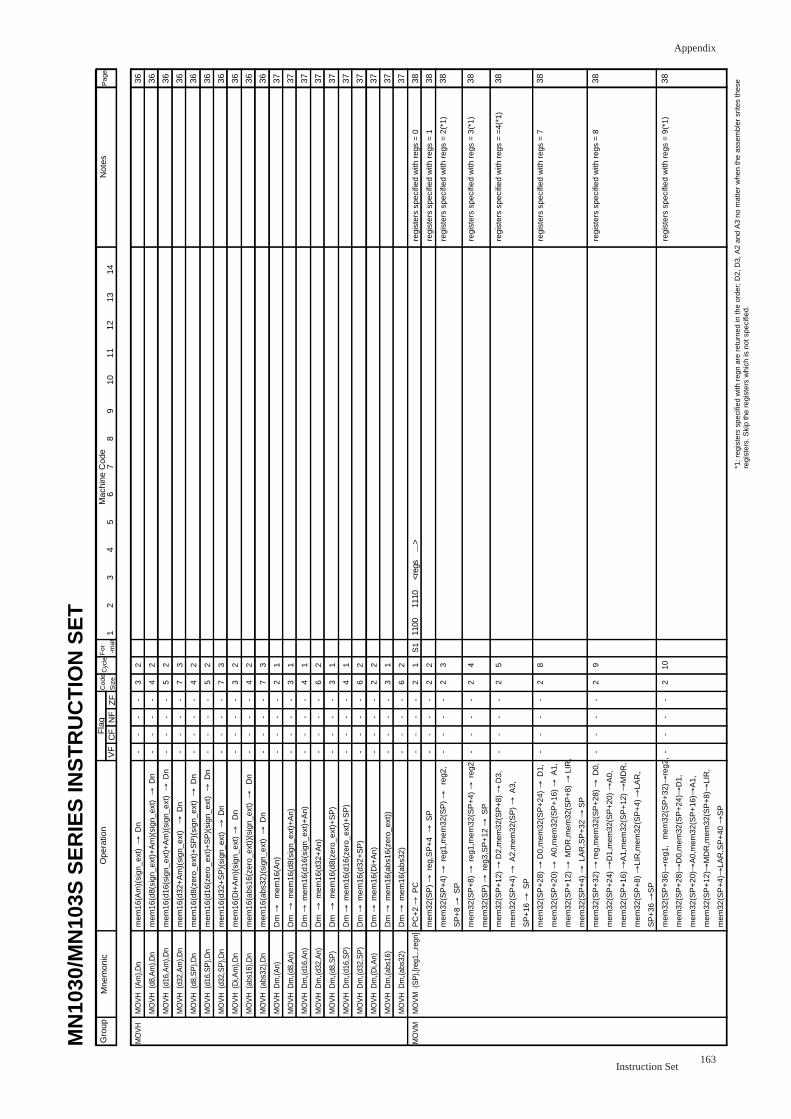
Appendix
163Instruction Set
MO
VH
(A
m),D
n�
MO
VH
(d8
,Am
),Dn�
MO
VH
(d1
6,A
m),D
n�
MO
VH
(d3
2,A
m),D
n�
MO
VH
(d8
,SP
),Dn�
MO
VH
(d1
6,S
P),D
n�
MO
VH
(d3
2,S
P),D
n�
MO
VH
(D
i,Am
),Dn�
MO
VH
(ab
s16)
,Dn�
MO
VH
(ab
s32)
,Dn�
MO
VH
Dm
,(An)
�
MO
VH
Dm
,(d8,
An)
�
MO
VH
Dm
,(d16
,An)
�
MO
VH
Dm
,(d32
,An)
�
MO
VH
Dm
,(d8,
SP
)�
MO
VH
Dm
,(d16
,SP
)�
MO
VH
Dm
,(d32
,SP
)�
MO
VH
Dm
,(Di,A
n)�
MO
VH
Dm
,(abs
16)�
MO
VH
Dm
,(abs
32)�
MO
VM
(S
P),[
reg1
,.,re
gn]
mem
16(A
m)(
sign
_ext
) →
Dn�
mem
16(d
8(si
gn_e
xt)+
Am
)(si
gn_e
xt)
→ D
n�
mem
16(d
16(s
ign_
ext)
+A
m)(
sign
_ext
) →
Dn�
mem
16(d
32+
Am
)(si
gn_e
xt)
→ D
n�
mem
16(d
8(ze
ro_e
xt)+
SP
)(si
gn_e
xt)
→ D
n�
mem
16(d
16(z
ero_
ext)
+S
P)(
sign
_ext
) →
Dn�
mem
16(d
32+
SP
)(si
gn_e
xt)
→ D
n�
mem
16(D
i+A
m)(
sign
_ext
) →
D
n�
mem
16(a
bs16
(zer
o_ex
t))(
sign
_ext
) →
D
n�
mem
16(a
bs32
)(si
gn_e
xt)
→ D
n�
Dm
→
mem
16(A
n)�
Dm
→ m
em16
(d8(
sign
_ext
)+A
n)�
Dm
→ m
em16
(d16
(sig
n_ex
t)+
An)
�
Dm
→ m
em16
(d32
+A
n)�
Dm
→ m
em16
(d8(
zero
_ext
)+S
P)�
Dm
→ m
em16
(d16
(zer
o_ex
t)+
SP
)�
Dm
→ m
em16
(d32
+S
P)�
Dm
→ m
em16
(Di+
An)
�
Dm
→ m
em16
(abs
16(z
ero_
ext)
)�
Dm
→ m
em16
(abs
32)�
PC
+2 →
PC
�
mem
32(S
P) →
reg
,SP
+4
→ S
P�
mem
32(S
P+
4) →
reg
1,m
em32
(SP
) →
re
g2,�
SP
+8 →
SP
�
mem
32(S
P+
8) →
reg
1,m
em32
(SP
+4)
→ r
eg2,
�
mem
32(S
P) →
reg
3,S
P+
12 →
SP
�
mem
32(S
P+
12) →
D2,
mem
32(S
P+
8) →
D3,
�
mem
32(S
P+
4) →
A2,
mem
32(S
P) →
A3,
�
SP
+16
→ S
P�
mem
32(S
P+
28) →
D0,
mem
32(S
P+
24) →
D1,
�
mem
32(S
P+
20) →
A0,
mem
32(S
P+
16) →
A1,
�
mem
32(S
P+
12) →
MD
R,m
em32
(SP
+8)
→ L
IR,�
mem
32(S
P+
4) →
LA
R,S
P+
32 →
SP
�
mem
32(S
P+
32) →
reg
,mem
32(S
P+
28) →
D0,
�
mem
32(S
P+
24) →
D1,
mem
32(S
P+
20) →
A0,
�
mem
32(S
P+
16) →
A1,
mem
32(S
P+
12) →
MD
R,�
mem
32(S
P+
8) →
LIR
,mem
32(S
P+
4) →
LAR
,�
SP
+36
→S
P�
mem
32(S
P+
36)→
reg1
,�m
em32
(SP
+32
)→re
g2,�
mem
32(S
P+
28)→
D0,
mem
32(S
P+
24)→
D1,
�
mem
32(S
P+
20)→
A0,
mem
32(S
P+
16)→
A1,
�
mem
32(S
P+
12)→
MD
R,m
em32
(SP
+8)→
LIR
,�
mem
32(S
P+
4)→
LAR
,SP
+40
→S
P�
� �
-� -� -� -� -� -� -� -� -� -� -� -� -� -� -� -� -� -� -� -� -� -� -� � -� � -� � � -� � � � -� � � � � -
-� -� -� -� -� -� -� -� -� -� -� -� -� -� -� -� -� -� -� -� -� -� -� � -� � -� � � -� � � � -� � � � � -
-� -� -� -� -� -� -� -� -� -� -� -� -� -� -� -� -� -� -� -� -� -� -� � -� � -� � � -� � � � -� � � � � -� �
-� -� -� -� -� -� -� -� -� -� -� -� -� -� -� -� -� -� -� -� -� -� -� � -� � -� � � -� � � � -� � � � � -
3� 4� 5� 7� 4� 5� 7� 3� 4� 7� 2� 3� 4� 6� 3� 4� 6� 2� 3� 6� 2� 2� 2� � 2� � 2� � � 2� � � � 2� � � � � 2
2� 2� 2� 3� 2� 2� 3� 2� 2� 3� 1� 1� 1� 2� 1� 1� 2� 2� 1� 2� 1� 2� 3� � 4� � 5� � � 8� � � � 9� � � � � 10
� � � � � � � � � � � � � � � � � � � �
S1
1� � � � � � � � � � � � � � � � � � � � � � 1100
2� � � � � � � � � � � � � � � � � � � � � � 1110
�
�
3� � � � � � � � � � � � � � � � � � � � � � <reg
s
4� � � � � � � � � � � � � � � � � � � � � � ....>
5� � �
6� � �
� �
Gro
up�
�
Mne
mon
icO
pera
tion
Mac
hine
Cod
eN
otes
Pag
eF
lag
Cod
e�
Siz
eC
ycle
For
�
-m
at
MN
1030
/MN
103S
SE
RIE
S IN
ST
RU
CT
ION
SE
T7� � �
8� � �
9� � �
10�
� �
11�
� �
12�
� �
1314
VF
CF
NF
ZF
MO
VH
�
� � � � � � � � � � � � � � � � � � � MO
VM
�� � � � � � � � � � � � � � � � � � � � re
gist
ers
spec
ified
with
reg
s =
0�
regi
ster
s sp
ecifi
ed w
ith r
egs
= 1
�
regi
ster
s sp
ecifi
ed w
ith r
egs
= 2
(*1)
�
� regi
ster
s sp
ecifi
ed w
ith r
egs
= 3
(*1)
�
� regi
ster
s sp
ecifi
ed w
ith r
egs
= =
4(*1
)�
� � regi
ster
s sp
ecifi
ed w
ith r
egs
= 7
�
� � � regi
ster
s sp
ecifi
ed w
ith r
egs
= 8
�
� � � � regi
ster
s sp
ecifi
ed w
ith r
egs
= 9
(*1)
�
� � �
*1: r
egis
ters
spe
cifie
d w
ith r
egn
are
retu
rned
in th
e or
der;
D2,
D3,
A2
and
A3
no m
atte
r w
hen
the
asse
mbl
er s
rites
thes
e �
regi
ster
s. S
kip
the
regi
ster
s w
hich
is n
ot s
peci
fied.
36�
36�
36�
36�
36�
36�
36�
36�
36�
36�
37�
37�
37�
37�
37�
37�
37�
37�
37�
37�
38�
38�
38� �
38� �
38� � �
38� � � �
38� � � � �
38� � � �
�
�
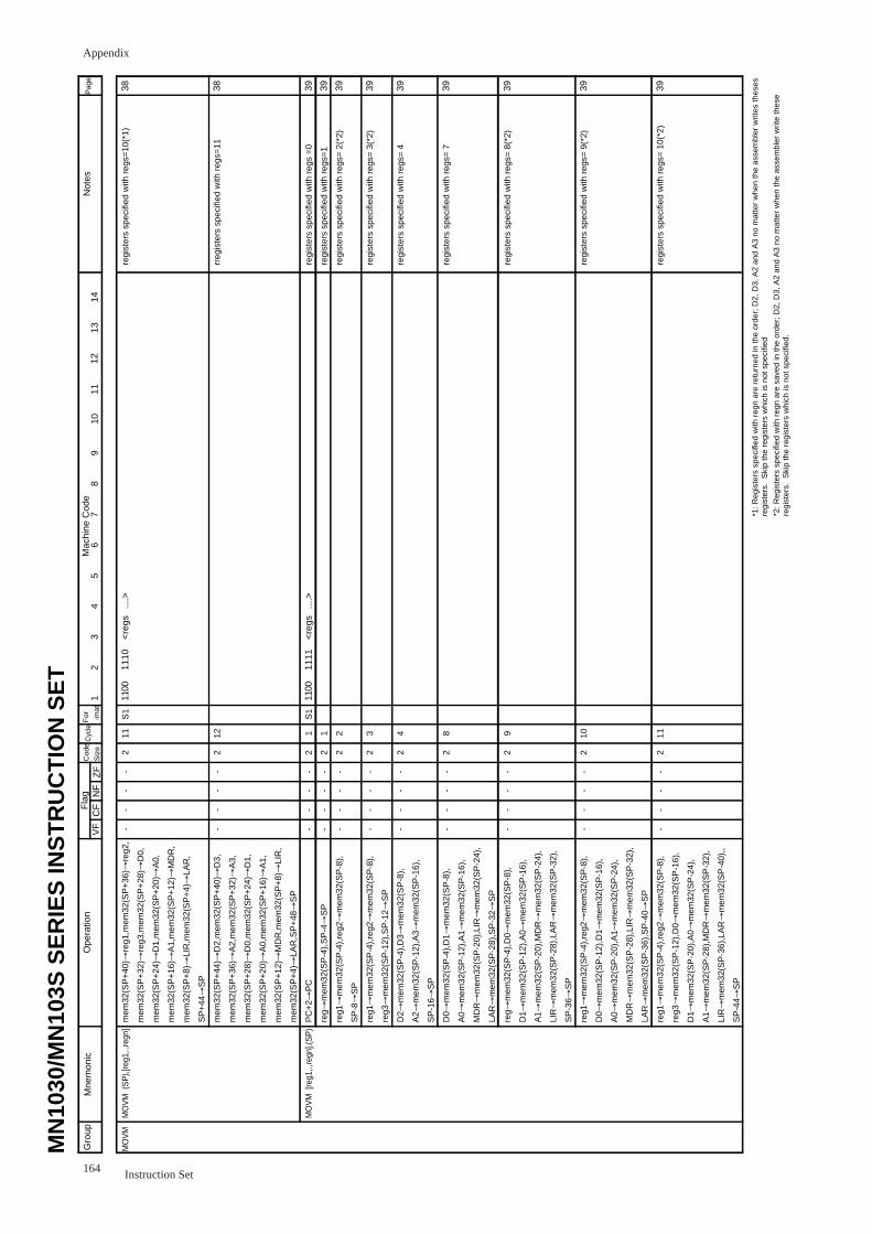
Appendix
164 Instruction Set
MO
VM
(S
P),[
reg1
,.,re
gn]�
� � � � � � � � � � � MO
VM
[re
g1,.,
regn
],(S
P)
mem
32(S
P+
40)→
reg1
,mem
32(S
P+
36)→
reg2
,�
mem
32(S
P+
32)→
reg3
,mem
32(S
P+
28)→
D0,
�
mem
32(S
P+
24)→
D1,
mem
32(S
P+
20)→
A0,
�
mem
32(S
P+
16)→
A1,
mem
32(S
P+
12)→
MD
R,�
mem
32(S
P+
8)→
LIR
,mem
32(S
P+
4)→
LAR
,�
SP
+44
→S
P�
mem
32(S
P+
44)→
D2,
mem
32(S
P+
40)→
D3,
�
mem
32(S
P+
36)→
A2,
mem
32(S
P+
32)→
A3,
�
mem
32(S
P+
28)→
D0,
mem
32(S
P+
24)→
D1,
�
mem
32(S
P+
20)→
A0,
mem
32(S
P+
16)→
A1,
�
mem
32(S
P+
12)→
MD
R,m
em32
(SP
+8)→
LIR
,�
mem
32(S
P+
4)→
LAR
,SP
+48
→S
P�
PC
+2→
PC
�
reg→
mem
32(S
P-4
),S
P-4→
SP
�
reg1
→m
em32
(SP
-4),
reg2
→m
em32
(SP
-8),
�
SP
-8→
SP
�
reg1
→m
em32
(SP
-4),
reg2
→m
em32
(SP
-8),
�
reg3
→m
em32
(SP
-12)
,SP
-12→
SP
�
D2→
mem
32(S
P-4
),D
3→m
em32
(SP
-8),
�
A2→
mem
32(S
P-1
2),A
3→m
em32
(SP
-16)
,�
SP
-16→
SP
�
D0→
mem
32(S
P-4
),D
1→m
em32
(SP
-8),
�
A0→
mem
32(S
P-1
2),A
1→m
em32
(SP
-16)
,�
MD
R→
mem
32(S
P-2
0),L
IR→
mem
32(S
P-2
4),�
LAR→
mem
32(S
P-2
8),S
P-3
2→S
P�
reg→
mem
32(S
P-4
),D
0→m
em32
(SP
-8),
�
D1→
mem
32(S
P-1
2),A
0→m
em32
(SP
-16)
,�
A1→
mem
32(S
P-2
0),M
DR→
mem
32(S
P-2
4),�
LIR→
mem
32(S
P-2
8),L
AR→
mem
32(S
P-3
2),�
SP
-36→
SP
�
reg1
→m
em32
(SP
-4),
reg2
→m
em32
(SP
-8),
�
D0→
mem
32(S
P-1
2),D
1→m
em32
(SP
-16)
,�
A0→
mem
32(S
P-2
0),A
1→m
em32
(SP
-24)
,�
MD
R→
mem
32(S
P-2
8),L
IR→
mem
32(S
P-3
2),�
LAR→
mem
32(S
P-3
6),S
P-4
0→S
P�
reg1
→m
em32
(SP
-4),
reg2
→m
em32
(SP
-8),
�
reg3
→m
em32
(SP
-12)
,D0→
mem
32(S
P-1
6),�
D1→
mem
32(S
P-2
0),A
0→m
em32
(SP
-24)
,�
A1→
mem
32(S
P-2
8),M
DR→
mem
32(S
P-3
2),�
LIR→
mem
32(S
P-3
6),L
AR→
mem
32(S
P-4
0),,�
SP
-44→
SP
�
�
-� � � � � � -� � � � � � -� -� -� � -� � -� � � -� � � � -� � � � � -� � � � � -� � �
-� � � � � � -� � � � � � -� -� -� � -� � -� � � -� � � � -� � � � � -� � � � � -
-� � � � � � -� � � � � � -� -� -� � -� � -� � � -� � � � -� � � � � -� � � � � -
-� � � � � � -� � � � � � -� -� -� � -� � -� � � -� � � � -� � � � � -� � � � � -� � � �
2� � � � � � 2� � � � � � 2� 2� 2� � 2� � 2� � � 2� � � � 2� � � � � 2� � � � � 2
11� � � � � � 12� � � � � � 1� 1� 2� � 3� � 4� � � 8� � � � 9� � � � � 10� � � � � 11
S1� � � � � � � � � � � �
S1
1� � 1100
�
� � � � � � � � � � � 1100
2� � 1110
�
� � � � � � � � � � � 1111
�
�
3� � <re
gs�
� � � � � � � � � � � <re
gs
4� � ....>
�
� � � � � � � � � � � ....>
5� � �
6� � �
� �
Gro
up�
�
Mne
mon
icO
pera
tion
Mac
hine
Cod
eN
otes
Pag
eF
lag
Cod
e�
Siz
eC
ycle
For
�
-m
at
MN
1030
/MN
103S
SE
RIE
S IN
ST
RU
CT
ION
SE
T7� � �
8� � �
9� �
10�
� �
11�
� �
12�
� �
1314
VF
CF
NF
ZF
MO
VM
�re
gist
ers
spec
ified
with
reg
s=10
(*1)
�
� � � � � rreg
iste
rs s
peci
fied
with
reg
s=11
�
� � � � � regi
ster
s sp
ecifi
ed w
ith r
egs
=0�
regi
ster
s sp
ecifi
ed w
ith r
egs=
1 �
regi
ster
s sp
ecifi
ed w
ith r
egs=
2(*
2)�
� regi
ster
s sp
ecifi
ed w
ith r
egs=
3(*
2)�
� regi
ster
s sp
ecifi
ed w
ith r
egs=
4�
� � regi
ster
s sp
ecifi
ed w
ith r
egs=
7�
� � � regi
ster
s sp
ecifi
ed w
ith r
egs=
8(*
2)�
� � � � regi
ster
s sp
ecifi
ed w
ith r
egs=
9(*
2)�
� � � � regi
ster
s sp
ecifi
ed w
ith r
egs=
10(
*2)�
�
*1: R
egis
ters
spe
cifie
d w
ith r
egn
are
retu
rned
in th
e or
der;
D2,
D3,
A2
and
A3
no m
atte
r w
hen
the
asse
mbl
er w
rites
thes
es
regi
ster
s. S
kip
the
regi
ster
s w
hich
is n
ot s
peci
fied
*2: R
egis
ters
spe
cifie
d w
ith r
egn
are
save
d in
the
orde
r; D
2, D
3, A
2 an
d A
3 no
mat
ter
whe
n th
e as
sem
bler
writ
e th
ese�
regi
ster
s. S
kip
the
regi
ster
s w
hich
is n
ot s
peci
fied.
38� � � � � �
38� � � � � �
39�
39�
39� �
39� �
39� � �
39� � � �
39� � � � �
39� � � � �
39
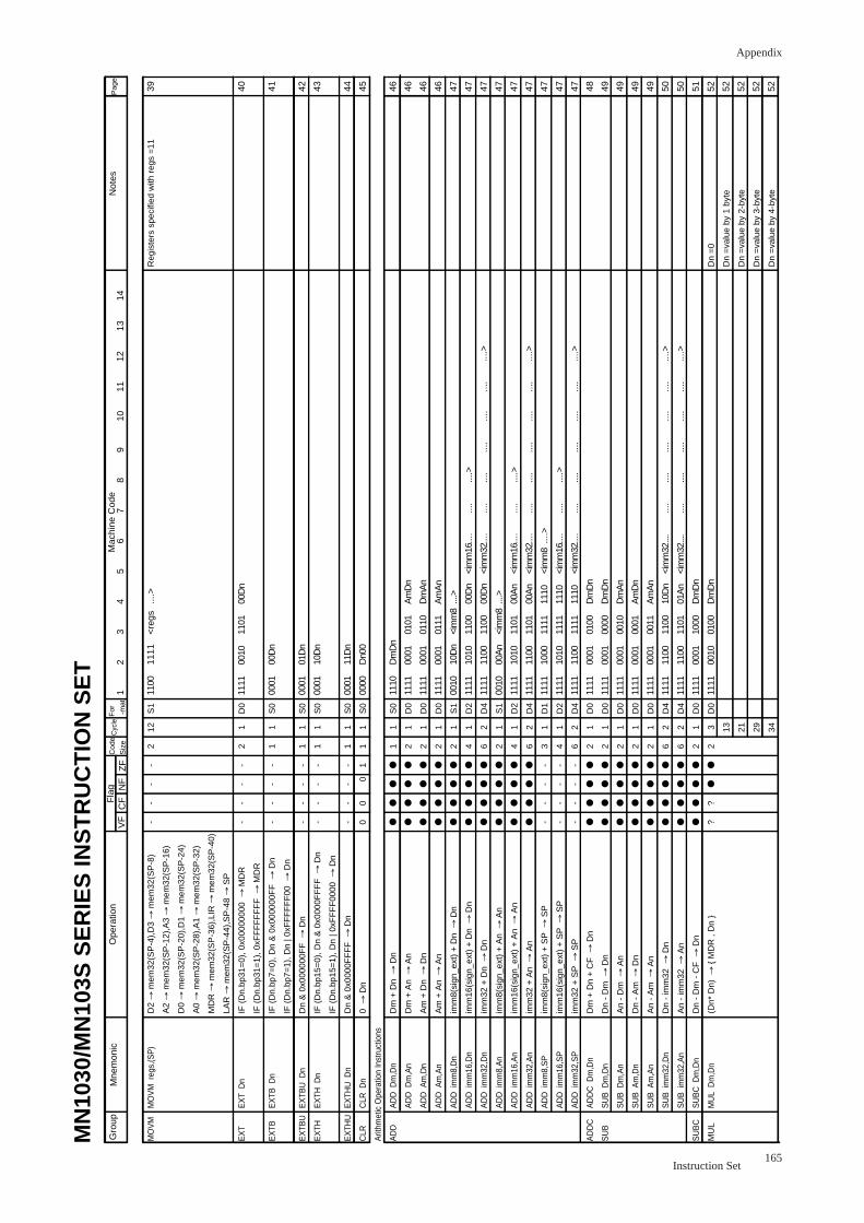
Appendix
165Instruction Set
MO
VM
reg
s,(S
P)�
� � � � � EX
T D
n�
� EX
TB D
n�
� EX
TBU
Dn�
EX
TH D
n�
� EX
THU
Dn�
CLR
Dn�
� AD
D D
m,D
n�
AD
D D
m,A
n�
AD
D A
m,D
n�
AD
D A
m,A
n�
AD
D i
mm
8,D
n�
AD
D i
mm
16,D
n�
AD
D i
mm
32,D
n�
AD
D i
mm
8,A
n�
AD
D i
mm
16,A
n�
AD
D i
mm
32,A
n�
AD
D i
mm
8,S
P�
AD
D i
mm
16,S
P�
AD
D i
mm
32,S
P�
AD
DC
Dm
,Dn�
SU
B D
m,D
n�
SU
B D
m,A
n�
SU
B A
m,D
n�
SU
B A
m,A
n�
SU
B i
mm
32,D
n�
SU
B i
mm
32,A
n�
SU
BC
Dm
,Dn�
MU
L D
m,D
n
D2 →
mem
32(S
P-4
),D
3 →
mem
32(S
P-8
)�
A2 →
mem
32(S
P-1
2),A
3 →
mem
32(S
P-1
6)�
D0 →
mem
32(S
P-2
0),D
1 →
mem
32(S
P-2
4)�
A0 →
mem
32(S
P-2
8),A
1 →
mem
32(S
P-3
2)�
MD
R →
mem
32(S
P-3
6),L
IR →
mem
32(S
P-4
0)�
LAR
→ m
em32
(SP
-44)
,SP
-48 →
SP
�
IF (
Dn.
bp31
=0)
, 0x0
0000
000
→ M
DR
�
IF (
Dn.
bp31
=1)
, 0xF
FF
FF
FF
F →
MD
R�
IF (
Dn.
bp7=
0), D
n &
0x0
0000
0FF
→ D
n�
IF (
Dn.
bp7=
1), D
n | 0
xFF
FF
FF
00 →
Dn�
Dn
& 0
x000
000F
F →
Dn
�
IF (
Dn.
bp15
=0)
, Dn
& 0
x000
0FF
FF
→ D
n�
IF (
Dn.
bp15
=1)
, Dn
| 0xF
FF
F00
00 →
Dn�
Dn
& 0
x000
0FF
FF
→ D
n�
0 →
Dn�
� Dm
+ D
n →
Dn�
Dm
+ A
n →
An�
Am
+ D
n →
Dn�
Am
+ A
n →
An�
imm
8(si
gn_e
xt)
+ D
n →
Dn�
imm
16(s
ign_
ext)
+ D
n →
Dn�
imm
32 +
Dn
→ D
n�
imm
8(si
gn_e
xt)
+ A
n →
An�
imm
16(s
ign_
ext)
+ A
n →
An�
imm
32 +
An
→ A
n�
imm
8(si
gn_e
xt)
+ S
P →
SP
�
imm
16(s
ign_
ext)
+ S
P →
SP
�
imm
32 +
SP
→ S
P�
Dm
+ D
n +
CF
→ D
n�
Dn
- D
m →
Dn�
An
- D
m →
An�
Dn
- A
m →
Dn�
An
- A
m →
An�
Dn
- im
m32
→ D
n�
An
- im
m32
→ A
n�
Dn
- D
m -
CF
→ D
n�
(Dn*
Dn)
→ {
MD
R ,
Dn
}�
� �
-� � � � � � -� � -� � -� -� � -� 0� ● ● ● ● ● ● ● ● ● ● -� -� -� ● ● ● ● ● ● ● ● ?
-� � � � � � -� � -� � -� -� � -� 0� � ● ● ● ● ● ● ● ● ● ●� -� -� -� ● ● ● ● ● ● ● ● ?
-� � � � � � -� � -� � -� -� � -� �0� � ● ● ● ● ● ● ● ● ● ●� -� -� -� ● ● ● ● ● ● ● ● ●
-� � � � � � -� � -� � -� -� � -� 1� � ● ● ● ● ● ● ● ● ● ● -� -� -� ● ● ● ● ● ● ● ● ●
2� � � � � � 2� � 1� � 1� 1� � 1� 1� � 1� 2� 2� 2� 2� 4� 6� 2� 4� 6� 3� 4� 6� 2� 2� 2� 2� 2� 6� 6� 2� 2
12� � � � � � 1� � 1� � 1� 1� � 1� 1� � 1� 1� 1� 1� 1� 1� 2� 1� 1� 2� 1� 1� 2� 1� 1� 1� 1� 1� 2� 2� 1� 3� 13�
21�
29�
34
S1� � � � � �
D0� �
S0� �
S0�
S0� �
S0�
S0� �
S0�
D0�
D0�
D0�
S1�
D2�
D4�
S1�
D2�
D4�
D1�
D2�
D4�
D0�
D0�
D0�
D0�
D0�
D4�
D4�
D0�
D0
1� � 1100
�
� � � � � 1111
�
� 0001
�
� 0001
�
0001
�
� 0001
�
0000
�
� 1110
�
1111
�
1111
�
1111
�
0010
�
1111
�
1111
�
0010
�
1111
�
1111
�
1111
�
1111
�
1111
�
1111
�
1111
�
1111
�
1111
�
1111
�
1111
�
1111
�
1111
�
1111
2� � 1111
�
� � � � � 0010
�
� 00D
n�
� 01D
n�
10D
n�
� 11D
n�
Dn0
0�
� Dm
Dn�
0001
�
0001
�
0001
�
10D
n�
1010
�
1100
�
00A
n�
1010
�
1100
�
1000
�
1010
�
1100
�
0001
�
0001
�
0001
�
0001
�
0001
�
1100
�
1100
�
0001
�
0010
3� � <re
gs�
� � � � � 1101
�
� � � � � � � � � � 0101
�
0110
�
0111
�
<im
m8�
1100
�
1100
�
<im
m8�
1101
�
1101
�
1111
�
1111
�
1111
�
0100
�
0000
�
0010
�
0001
�
0011
�
1100
�
1101
�
1000
�
0100
�
� � � � �
4� � ....>
�
� � � � � 00D
n�
� � � � � � � � � � Am
Dn�
Dm
An�
Am
An�
....>
�
00D
n�
00D
n�
....>
�
00A
n�
00A
n�
1110
�
1110
�
1110
�
Dm
Dn�
Dm
Dn�
Dm
An�
Am
Dn�
Am
An�
10D
n�
01A
n�
Dm
Dn�
Dm
Dn
5� � � � � � � � � � � � � � � � � � � � � � � <im
m16
�
<im
m32
�
� <im
m16
�
<im
m32
�
<im
m8�
<im
m16
�
<im
m32
�
� � � � � <im
m32
....�
<im
m32
....�
� �
6� � � � � � � � � � � � � � � � � � � � � � � ....�
....�
� ....�
....�
....>
�
....�
....
� �
Gro
up�
�
Mne
mon
icO
pera
tion
Mac
hine
Cod
eN
otes
Pag
eF
lag
Cod
e�
Siz
eC
ycle
For
�
-m
at
MN
1030
/MN
103S
SE
RIE
S IN
ST
RU
CT
ION
SE
T7� � � � � � � � � � � � � � � � � � � � � � � ...
.�
....�
� ....�
....�
� ....�
....�
� � � � � ....�
....
8� � � � � � � � � � � � � � � � � � � � � � � ....>
�
....�
� ....>
�
....�
� ....>
�
....�
� � � � � ....�
....
9� � � � � � � � � � � � � � � � � � � � � � � � ....�
� � ....�
� � ....�
� � � � � ....�
....
10�
� � � � � � � � � � � � � � � � � � � � � � � ....�
� � ....�
� � ....�
� � � � � ....�
....
11�
� � � � � � � � � � � � � � � � � � � � � � � ....�
� � ....�
� � ....�
� � � � � ....�
....
12�
� � � � � � � � � � � � � � � � � � � � � � � ....>
�
� � ....>
�
� � ....>
�
� � � � � ....>
�
....>
1314
VF
CF
NF
ZF
MO
VM
�
� � � � � EX
T�
� EX
TB�
� EX
TBU
�
EX
TH�
� EX
THU
�
CLR
�
Arit
hmet
ic O
pera
tion
Inst
ruct
ions
�
AD
D�
� � � � � � � � � � � � AD
DC
�
SU
B�
� � � � � SU
BC
�
MU
L
�
�
Reg
iste
rs s
peci
fied
with
reg
s =
11�
� � � � � � � � � � � � � � � � � � � � � � � � � � � � � � � � � � � � Dn
=0�
Dn
=va
lue
by 1
byt
e �
Dn
=va
lue
by 2
-byt
e �
Dn
=va
lue
by 3
-byt
e �
Dn
=va
lue
by 4
-byt
e �
�
39� � � � � �
40� �
41� �
42�
43� �
44�
45� �
46�
46�
46�
46�
47�
47�
47�
47�
47�
47�
47�
47�
47�
48�
49�
49�
49�
49�
50�
50�
51�
52�
52�
52�
52�
52
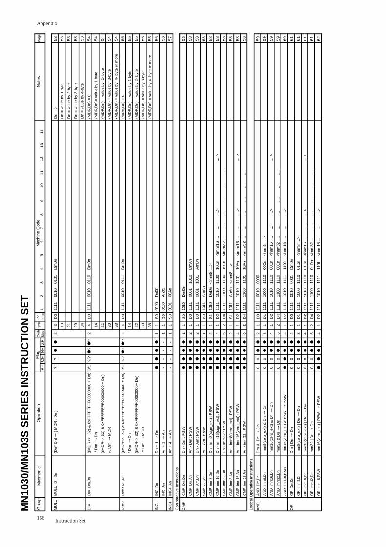
Appendix
166 Instruction Set
MU
LU D
m,D
n�
� � � � DIV
Dm
,Dn�
� � � � DIV
U D
m,D
n�
� � � � INC
Dn�
INC
An�
INC
4 A
n�
� CM
P D
m,D
n�
CM
P D
m,A
n�
CM
P A
m,D
n�
CM
P A
m,A
n�
CM
P i
mm
8,D
n�
CM
P i
mm
16,D
n�
CM
P i
mm
32,D
n�
CM
P i
mm
8,A
n�
CM
P i
mm
16,A
n�
CM
P i
mm
32,A
n�
� AN
D D
m,D
n�
AN
D i
mm
8,D
n�
AN
D i
mm
16,D
n�
AN
D i
mm
32,D
n�
AN
D i
mm
16,P
SW
�
OR
Dm
,Dn�
OR
im
m8,
Dn�
OR
im
m16
,Dn�
OR
im
m32
,Dn�
OR
im
m16
,PS
W�
�
(Dn*
Dn)
→ {
MD
R ,
Dn
}�
� � � � ((M
DR
<<
�32
) &
0xF
FF
FF
FF
F00
0000
00 +
Dn)
�
/ D
m →
Dn�
((M
DR
<<
32)
& 0
xFF
FF
FF
FF
0000
0000
+ D
n) �
% D
m →
MD
R�
� ((M
DR
<<
�32
) &
0xF
FF
FF
FF
F00
0000
00 +
Dn)
�
/ Dm
→ D
n�
((M
DR
<<
32)
& 0
xFF
FF
FF
FF
0000
0000
+ D
n) �
% D
m →
MD
R�
� Dn
+ 1
→ D
n�
An
+ 1
→ A
n�
An
+ 4
→ A
n�
� Dn
- D
m :
PS
W�
An
- D
m :
PS
W�
Dn
- A
m :
PS
W�
An
- A
m :
PS
W�
Dn
- im
m8(
sign
_ext
) : P
SW
�
Dn
- im
m16
(sig
n_ex
t) :
PS
W�
Dn
- im
m32
: P
SW
�
An
- im
m8(
zero
_ext
) : P
SW
�
An
- im
m16
(zer
o_ex
t) :
PS
W�
An
- im
m32
: P
SW
�
� Dm
& D
n →
Dn�
imm
8(ze
ro_e
xt)
& D
n →
Dn�
imm
16(z
ero_
ext)
& D
n →
Dn�
imm
32 &
Dn
→ D
n�
imm
16(z
ero_
ext)
& P
SW
→ P
SW
�
Dm
| D
n →
Dn�
imm
8(ze
ro_e
xt)
| Dn
→ D
n�
imm
16(z
ero_
ext)
| D
n →
Dn�
imm
32 |
Dn
→ D
n�
imm
16(z
ero_
ext)
| P
SW
→ P
SW
�
�
?� � � � �
0/1� � � � �
0/1� � � � � ●� -� -� � ● ● ● ● ● ● ● ● ● ●� � 0� 0� 0� 0� ●�
0� 0� 0� 0� ●
?� � � � �
?/?� � � � �
?/?� � � � � ●� -� -� � ● ● ● ● ● ● ● ● ● ● � 0� 0� 0� 0� ●�
0� 0� 0� 0� ●
●� � � � �
●/?
�
� � � �
●/?
�
� � � � ●� -� -� � ● ● ● ● ● ● ● ● ● ● ● ● ● ● ● ● ● ● ● ●
●� � � � �
●/?
�
� � � �
●/?
�
� � � � ●� -� -� � ● ● ● ● ● ● ● ● ● ● ● ● ● ● ● ● ● ● ● ●
2� � � � � 2� � � � � 2� � � � � 1� 1� 1� � 1� 2� 2� 1� 2� 4� 6� 2� 4� 6� � 2� 3� 4� 6� 4� 2� 3� 4� 6� 4
3� 13�
21�
29�
34�
4� 14�
22�
30�
38�
4� 14�
22�
30�
38�
1� 1� 1� � 1� 1� 1� 1� 1� 1� 2� 1� 1� 2� � 1� 1� 1� 2� 1� 1� 1� 1� 2� 1
D0� � � � �
D0� � � � �
D0� � � � �
S0�
S0�
S0� �
S0�
D0�
D0�
S0�
S1�
D2�
D4�
S1�
D2�
D4� �
D0�
D1�
D2�
D4�
D2�
D0�
D1�
D2�
D4�
D2� �
1� � 1111
�
� � � � 1111
�
� � � � 1111
�
� � � � 0100
�
0100
�
0101
�
� 1010
�
1111
�
1111
�
1011
�
1010
�
1111
�
1111
�
1011
�
1111
�
1111
�
� 1111
�
1111
�
1111
�
1111
�
1111
�
1111
�
1111
�
1111
�
1111
�
1111
�
�
2� � 0010
�
� � � � 0010
�
� � � � 0010
�
� � � � Dn0
0�
An0
1�
00A
n�
� Dm
Dn�
0001
�
0001
�
Am
An�
DnD
n�
1010
�
1100
�
AnA
n�
1010
�
1100
�
� 0010
�
1000
�
1010
�
1100
�
1010
�
0010
�
1000
�
1010
�
1100
�
1010
3� � 0101
�
� � � � 0110
�
� � � � 0111
�
� � � � � � � � � 1010
�
1001
�
� <im
m8�
1100
�
1100
�
<im
m8�
1101
�
1101
�
� 0000
�
1110
�
1110
�
1110
�
1111
�
0001
�
1110
�
1110
�
1110
�
1111
�
4� � Dm
Dn�
� � � � Dm
Dn�
� � � � Dm
Dn�
� � � � � � � � � Dm
An�
Am
Dn�
� ....>
�
10D
n�
10D
n�
....>
�
10A
n�
10A
n�
� � 00D
n�
00D
n�
00D
n�
1100
�
Dm
Dn�
01D
n�
01D
n�
0�D
n�
1101
�
�
5� � � � � � � � � � � � � � � � � � � � � � � � � � <im
m16
�
<im
m32
�
� <im
m16
�
<im
m32
�
� � <im
m8�
<im
m16
�
<im
m32
�
<im
m16
�
� <im
m8�
<im
m16
�
<im
m32
�
<im
m16
6� � � � � � � � � � � � � � � � � � � � � � � � � � ....
�
....
�
� ....
�
....
�
� � ....>
�
....
�
....
�
....
�
� ....>
�
....�
....�
....�
�
� �
Gro
up�
�
Mne
mon
icO
pera
tion
Mac
hine
Cod
eN
otes
Pag
eF
lag
Cod
e�
Siz
eC
ycle
For
�
-m
at
MN
1030
/MN
103S
SE
RIE
S IN
ST
RU
CT
ION
SE
T7� � � � � � � � � � � � � � � � � � � � � � � � � � ...
.�
....�
� ....�
....�
� � � ....�
....�
....�
� � ....�
....�
....�
�
8� � � � � � � � � � � � � � � � � � � � � � � � � � ....>
�
....�
� ....>
�
....�
� � � ....>
�
....�
....>
�
� � ....>
�
....�
....>
�
�
9� � � � � � � � � � � � � � � � � � � � � � � � � � � ....�
� � ....�
� � � � ....�
� � � � ....�
�
10�
� � � � � � � � � � � � � � � � � � � � � � � � � � ....�
� � ....�
� � � � ....�
� � � � ....�
�
11�
� � � � � � � � � � � � � � � � � � � � � � � � � � ....�
� � ....�
� � � � ....�
� � � � ....�
�
12�
� � � � � � � � � � � � � � � � � � � � � � � � � ....>
�
� � ....>
�
� � � � ....>
�
� � � � ....>
�
�
1314
�
VF
CF
NF
ZF
MU
LU�
� � � � DIV
�
� � � � DIV
U�
� � � � INC
�
� INC
4�
Com
para
tive
Inst
ruct
ions
�
CM
P�
� � � � � � � � � Logi
cal O
pera
tion
Inst
ruct
ions
�
AN
D�
� � � � OR
�D
n =
0�
Dn
= v
alue
by
1 by
te�
Dn
= v
alue
by
2-by
te�
Dn
= v
alue
by
3-by
te�
Dn
= v
alue
by
4-by
te�
{MD
R,D
n} =
0�
{MD
R,D
n}=
val
ue b
y 1
byte
�
{MD
R,D
n} =
val
ue b
y 2
- by
te�
{MD
R,D
n} =
val
ue b
y 3
-byt
e�
{MD
R,D
n} =
val
ue b
y 4
- by
te o
r m
ore�
{MD
R,D
n} =
0�
{MD
R,D
n} =
val
ue b
y 1
byte
�
{MD
R,D
n} =
val
ue b
y 2-
byt
e�
{MD
R,D
n} =
val
ue b
y 3-
byte
�
{MD
R,D
n} =
val
ue b
y 4-
byt
e or
mor
e�
� � � � � � � � � � � � � � � � � � � � �
53�
53�
53�
53�
53�
54�
54�
54�
54�
54�
55�
55�
55�
55�
55�
56�
56�
57� �
58�
58�
58�
58�
58�
58�
58�
58�
58�
58� �
59�
59�
59�
59�
60�
61�
61�
61�
61�
62
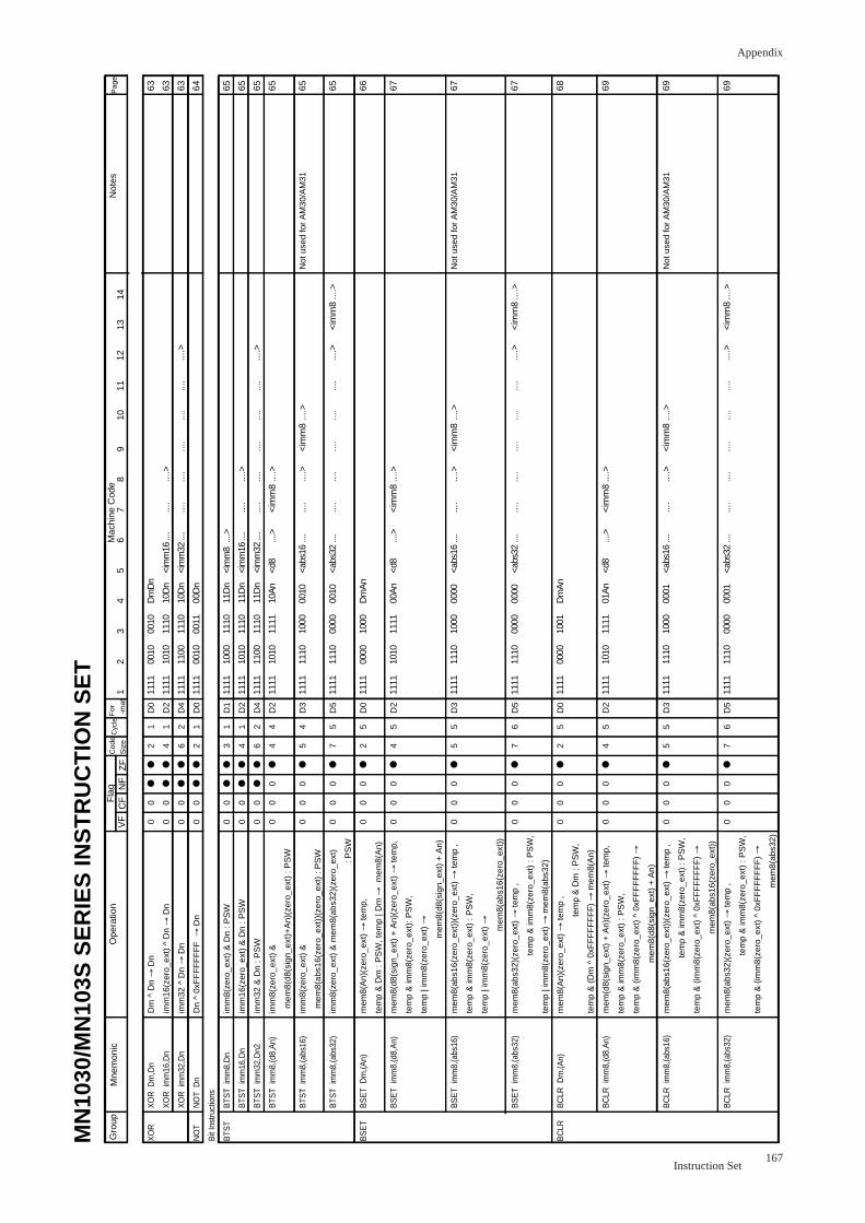
Appendix
167Instruction Set
XO
R D
m,D
n�
XO
R i
mm
16,D
n�
XO
R i
mm
32,D
n�
NO
T D
n�
� BTS
T im
m8,
Dn�
BTS
T im
m16
,Dn�
BTS
T im
m32
,Dn2
�
BTS
T im
m8,
(d8,
An)
�
� BTS
T im
m8,
(abs
16)�
� BTS
T im
m8,
(abs
32)�
� BS
ET
Dm
,(An)
�
� BS
ET
imm
8,(d
8,A
n)�
� � � BS
ET
imm
8,(a
bs16
)�
� � � BS
ET
imm
8,(a
bs32
)�
� � BC
LR D
m,(A
n)�
� � BC
LR i
mm
8,(d
8,A
n)�
� � � BC
LR i
mm
8,(a
bs16
)�
� � � BC
LR i
mm
8,(a
bs32
)
Dm
^ D
n →
Dn�
imm
16(z
ero_
ext)
^ D
n →
Dn�
imm
32 ^
Dn →
Dn�
Dn
^ 0x
FF
FF
FF
FF
→ D
n�
� imm
8(ze
ro_e
xt)
& D
n : P
SW
�
imm
16(z
ero_
ext)
& D
n : P
SW
�
imm
32 &
Dn
: PS
W�
imm
8(ze
ro_e
xt)
& �
mem
8(d8
(sig
n_ex
t)+
An)
(zer
o_ex
t) :
PS
W�
imm
8(ze
ro_e
xt)
&�
mem
8(ab
s16(
zero
_ext
))(z
ero_
ext)
: P
SW
�
imm
8(ze
ro_e
xt)
& m
em8(
abs3
2)(z
ero_
ext)
�
: P
SW
�
mem
8(A
n)(z
ero_
ext)
→ te
mp,
�
tem
p &
Dm
: P
SW
, tem
p | D
m →
mem
8(A
n)�
mem
8(d8
(sig
n_ex
t) +
An)
(zer
o_ex
t) →
tem
p,�
tem
p &
imm
8(ze
ro_e
xt):
PS
W, �
tem
p | i
mm
8(ze
ro_e
xt) →
�
mem
8(d8
(sig
n_ex
t) +
An)
�
mem
8(ab
s16(
zero
_ext
))(z
ero_
ext)
→ te
mp
, �
tem
p &
imm
8(ze
ro_e
xt)
: PS
W, �
tem
p | i
mm
8(ze
ro_e
xt) →
�
�
m
em8(
abs1
6(ze
ro_e
xt))
�
mem
8(ab
s32)
(zer
o_ex
t) →
tem
p , �
�
tem
p &
imm
8(ze
ro_e
xt)
: PS
W, �
tem
p | i
mm
8(ze
ro_e
xt) →
mem
8(ab
s32)
�
mem
8(A
n)(z
ero_
ext)
→ te
mp
, �
�
t
emp
& D
m :
PS
W,�
tem
p &
(D
m ^
0xF
FF
FF
FF
F) →
mem
8(A
n)�
mem
(d8(
sign
_ext
) +
An)
(zer
o_ex
t) →
tem
p, �
tem
p &
imm
8(ze
ro_e
xt)
: PS
W,�
tem
p &
(im
m8(
zero
_ext
) ^
0xF
FF
FF
FF
F) →
�
� m
em8(
d8(s
ign_
ext)
+ A
n)�
mem
8(ab
s16(
zero
_ext
))(z
ero_
ext)
→ te
mp
, �
�
tem
p &
imm
8(ze
ro_e
xt)
: PS
W,�
tem
p &
(im
m8(
zero
_ext
) ^
0xF
FF
FF
FF
F) →
�
�
m
em8(
abs1
6(ze
ro_e
xt))
�
mem
8(ab
s32)
(zer
o_ex
t) →
tem
p , �
�
tem
p &
imm
8(ze
ro_e
xt)
: PS
W,�
tem
p &
(im
m8(
zero
_ext
) ^
0xF
FF
FF
FF
F) →
�
��
mem
8(ab
s32)
Gro
up�
�
Mne
mon
icO
pera
tion
Pag
e
MN
1030
/MN
103S
SE
RIE
S IN
ST
RU
CT
ION
SE
T
XO
R�
� � NO
T�
Bit
Inst
ruct
ions
�
BTS
T�
� � � � � � � � BS
ET�
� � � � � � � � � � � � BC
LR
0� 0� 0� 0� � 0� 0� 0� 0� � 0� � 0� � 0� � 0� � � � 0� � � � 0� � � 0� � � 0� � � � 0� � � � 0
0� 0� 0� 0� � 0� 0� 0� 0� � 0� � 0� � 0� � 0� � � � 0� � � � 0� � � 0� � � 0� � � � 0� � � � 0
●�
●�
●�
●� � ●�
●�
●�
0� � 0� � 0� � 0� � 0� � � � 0� � � � 0� � � 0� � � 0� � � � 0� � � � 0
● ● ● ● ● ● ● ● ● ● ● ● ● ● ● ● ● ●
2� 4� 6� 2� � 3� 4� 6� 4� � 5� � 7� � 2� � 4� � � � 5� � � � 7� � � 2� � � 4� � � � 5� � � � 7
1� 1� 2� 1� � 1� 1� 2� 4� � 4� � 5� � 5� � 5� � � � 5� � � � 6� � � 5� � � 5� � � � 5� � � � 6
D0�
D2�
D4�
D0� �
D1�
D2�
D4�
D2� �
D3� �
D5� �
D0� �
D2� � � �
D3� � � �
D5� � �
D0� � �
D2� � � �
D3� � � �
D5
1� � 1111
�
1111
�
1111
�
1111
�
� 1111
�
1111
�
1111
�
1111
�
� 1111
�
� 1111
�
� 1111
�
� 1111
�
� � � 1111
�
� � � 1111
�
� � 1111
�
� � 1111
�
� � � 1111
�
� � � 1111
2� � 0010
�
1010
�
1100
�
0010
�
� 1000
�
1010
�
1100
�
1010
�
� 1110
�
� 1110
�
� 0000
�
� 1010
�
� � � 1110
�
� � � 1110
�
� � 0000
�
� � 1010
�
� � � 1110
�
� � � 1110
3� � 0010
�
1110
�
1110
�
0011
�
� 1110
�
1110
�
1110
�
1111
�
� 1000
�
� 0000
�
� 1000
�
� 1111
�
� � � 1000
�
� � � 0000
�
� � 1001
�
� � 1111
�
� � � 1000
�
� � � 0000
4� � Dm
Dn�
10D
n�
10D
n�
00D
n�
� 11D
n�
11D
n�
11D
n�
10A
n�
� 0010
�
� 0010
�
� Dm
An�
� 00A
n�
� � � 0000
�
� � � 0000
�
� � Dm
An�
� � 01A
n�
� � � 0001
�
� � � 0001
5� � � <im
m16
�
<im
m32
�
� � <im
m8�
<im
m16
�
<im
m32
�
<d8�
� <abs
16�
� <abs
32�
� � � <d8�
� � � <abs
16�
� � � <abs
32�
� � � � � <d8�
� � � <abs
16�
� � � <abs
32�
�
6� � � ....�
....�
� � ....>
�
....�
....�
....>
�
� ....�
� ....�
� � � ....>
�
� � � ....�
� � � ....�
� � � � � ....>
�
� � � ....�
� � � ....�
�
� �
Mac
hine
Cod
eF
lag
Cod
e�
Siz
eC
ycle
For
�
-m
at7� � � ...
.�
....�
� � � ....�
....�
<im
m8�
� ....�
� ....�
� � � <im
m8�
� � � ....�
� � � ....�
� � � � � <im
m8�
� � � ....�
� � � ....
8� � � ....>
�
....�
� � � ....>
�
....�
....>
�
� ....>
�
� ....�
� � � ....>
�
� � � ....>
�
� � � ....�
� � � � � ....>
�
� � � ....>
�
� � � ....
9� � � � ....�
� � � � ....�
� � <im
m8�
� ....�
� � � � � � � <im
m8�
� � � ....�
� � � � � � � � � <im
m8�
� � � ....
10�
� � � ....�
� � � � ....�
� � ....>
�
� ....�
� � � � � � � ....>
�
� � � ....�
� � � � � � � � � ....>
�
� � � ....�
�
11�
� � � ....�
� � � � ....�
� � � � ....�
� � � � � � � � � � � ....�
� � � � � � � � � � � � � ....
12�
� � � ....>
�
� � � � ....>
�
� � � � ....>
�
� � � � � � � � � � � ....>
�
� � � � � � � � � � � � � ....>
13�
� � � � � � � � � � � � � <im
m8�
� � � � � � � � � � � <im
m8�
� � � � � � � � � � � � � <im
m8
14�
� � � � � � � � � � � � � ....>
�
� � � � � � � � � � � ....>
�
� � � � � � � � � � � � � ....>
VF
CF
NF
ZF
�63
�
63�
63�
64� �
65�
65�
65�
65� �
65� �
65� �
66� �
67� � � �
67� � � �
67� � �
68� � �
69� � � �
69� � � �
69
Not
es
� � � � � � � � � � Not
use
d fo
r A
M30
/AM
31�
� � � � � � � � � Not
use
d fo
r A
M30
/AM
31�
� � � � � � � � � � � � � Not
use
d fo
r A
M30
/AM
31�
� � � �
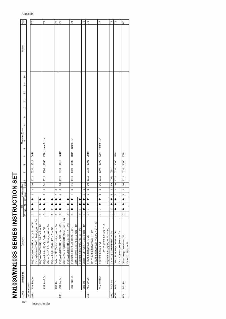
Appendix
168 Instruction Set
AS
R D
m,D
n�
� � AS
R i
mm
8,D
n�
� � AS
R D
n�
LSR
Dm
,Dn�
� � LSR
im
m8,
Dn�
� � LSR
Dn�
AS
L D
m,D
n�
� � AS
L im
m8,
Dn�
� � AS
L2 D
n�
RO
R D
n�
� RO
L D
n�
�
IF (
(Dm
&0x
0000
001F
) ≠
0) ,
Dn.
lsb →
CF
, �
(Dn
>>
(D
m &
0x0
0000
01F
))(s
ign_
ext)
→ D
n�
IF (
(Dm
&0x
0000
001F
)=0)
,PC
+ 2
→ P
C�
IF (
(imm
8 &
0x1
F) ≠0
) , D
n.ls
b →
CF
,�
(D
n >
> (
imm
8 &
0x1
F))
(sig
n_ex
t) →
Dn�
IF (
(imm
8 &
0x1
F)=
0) ,
PC
+ 3
→ P
C�
Dn.
lsb →
CF
, (D
n >
> 1
)(si
gn_e
xt) →
Dn�
IF (
(Dm
&0x
0000
001F
) ≠
0),D
n.ls
b →
CF
,�
(D
n >
> (
Dm
& 0
x000
0001
F))
(zer
o_ex
t) →
Dn�
IF (
(Dm
&0x
0000
001F
)=0)
, PC
+ 2
→ P
C�
IF (
(imm
8 &
0x1
F) ≠
0),D
n.ls
b →
CF
,�
(D
n >
> (
imm
8 &
0x1
F))
(zer
o_ex
t) →
Dn�
IF (
(imm
8 &
0x1
F)=
0), P
C +
3 →
PC
�
Dn.
lsb →
CF
, (D
n >
> 1
)(ze
ro_e
xt) →
Dn�
IF (
(Dm
& 0
x000
0001
F) ≠
0),�
Dn
<<
(D
m &
0x0
0000
01F
) →
Dn�
IF (
(Dm
& 0
x000
0001
F)=
0), P
C +
2 →
PC
�
IF (
(imm
8 &
0x1
F) ≠0
), �
�D
n <
< (
imm
8 &
0x1
F) →
Dn�
IF (
(imm
8 &
0x1
F)=
0), P
C +
3 →
PC
�
(Dn
<<
2 )
& 0
xFF
FF
FF
FC
→ D
n�
CF
<<
31 →
tem
p, D
n.ls
b →
CF
, �
(Dn
>>
1)(
zero
_ext
) | t
emp →
Dn�
CF
→
tem
p, D
n.m
sb →
CF
, �
(Dn
<<
1)
| tem
p →
Dn�
�
Gro
up�
�
Mne
mon
icO
pera
tion
Pag
e
MN
1030
/MN
103S
SE
RIE
S IN
ST
RU
CT
ION
SE
T
Shi
ft In
stru
ctio
ns�
AS
R�
� � � � � � LSR
�
� � � � � � AS
L�
� � � � � AS
L2�
RO
R�
� RO
L�
�
?� � ?� ?� � ?� ?� ?� � ?� ?� � ?� ?� ?� � � ?� � � ?� 0� � 0� �
● ?� ●� � ?� ●�
●� � ?� ●� � ?� ●�
?� � � ?� � � ?� ●� � ●� � �
●� � ●�
●� � ●�
● ● ● ● ● ● ● ● ● ● ●
● ● ● ● ● ● ● ● ● ● ● ● ● ● ●
2� � � 3� � � 3� 2� � � 3� � � 3� 2� � � 3� � � 1� 2� � 2� �
1� � � 1� � � 1� 1� � � 1� � � 1� 1� � � 1� � � 1� 1� � 1� �
D0� � �
D1� � � �
D0� � �
D1� � � �
D0� � �
D1� � �
S0�
D0� �
D0� �
1� � 1111
�
� � 1111
�
� � � 1111
�
� � 1111
�
� � � 1111
�
� � 1111
�
� � 0101
�
1111
�
� 1111
�
� � �
2� � 0010
�
� � 1000
�
� � � 0010
�
� � 1000
�
� � � 0010
�
� � 1000
�
� � 01D
n�
0010
�
� 0010
3� � 1011
�
� � 1100
�
� � � 1010
�
� � 1100
�
� � � 1001
�
� � 1100
�
� � � 1000
�
� 1000
4� � Dm
Dn�
� � 10D
n�
� � � Dm
Dn�
� � 01D
n�
� � � Dm
Dn�
� � 00D
n�
� � � 01D
n�
� 00D
n
5� � � � � <im
m8�
� � � � � � <im
m8�
� � � � � � <im
m8�
�
6� � � � � ....>
�
� � � � � � ....>
�
� � � � � � ....>
� �
Mac
hine
Cod
eF
lag
Cod
e�
Siz
eC
ycle
For
�
-m
at7� � �
8� � �
9� � �
10�
�
11�
� �
12�
� �
13�
� �
14�
� �
VF
CF
NF
ZF
70� � �
71� � �
72�
73� � �
74� � �
75�
76� � �
77� � �
78�
79� �
80
Not
es
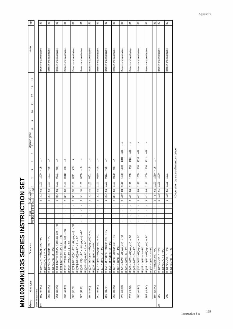
Appendix
169Instruction Set
BE
Q (
d8,P
C)�
� BN
E (
d8,P
C)�
� BG
T (d
8,P
C)�
� BG
E (
d8,P
C)�
� BLE
(d8
,PC
)�
� BLT
(d8
,PC
)�
� BH
I (d
8,P
C)�
� BC
C (
d8,P
C)�
� BLS
(d8
,PC
)�
� BC
S (
d8,P
C)�
� BV
C (
d8,P
C)�
� BV
S (
d8,P
C)�
� BN
C (
d8,P
C)�
� BN
S (
d8,P
C)�
� BR
A (
d8,P
C)�
LEQ
�
� LNE
�
� �
IF (
ZF
=1)
, PC
+ d
8(si
gn_e
xt)→
PC
�
IF (
ZF
=0)
,PC
+ 2
→ P
C�
IF (
ZF
=0)
, PC
+ d
8(si
gn_e
xt) →
PC
�
IF (
ZF
=1)
, PC
+ 2
→ P
C�
IF (
(ZF
| (N
F^V
F))
=0)
,PC
+ d
8(si
gn_e
xt) →
PC
�
IF (
(ZF
| (N
F^V
F))
=1)
,PC
+ 2
→ P
C�
IF (
(NF
^ V
F)=
0),P
C +
d8(
sign
_ext
) →
PC
�
IF (
(NF
^ V
F)=
1),P
C +
2 →
PC
�
IF (
(ZF
| (N
F^V
F))
=1)
,PC
+ d
8(si
gn_e
xt) →
PC
�
IF (
(ZF
| (N
F^V
F))
=0)
,PC
+ 2
→ P
C�
IF (
(NF
^ V
F)=
1),P
C +
d8(
sign
_ext
) →
PC
�
IF (
(NF
^ V
F)=
0),P
C +
2 →
PC
�
IF (
(CF
| Z
F)=
0),P
C +
d8(
sign
_ext
) →
PC
�
IF (
(CF
| Z
F)=
1),P
C +
2 →
PC
�
IF (
CF
= 0
),P
C +
d8(
sign
_ext
) →
PC
�
IF (
CF
= 1
),P
C +
2 →
PC
�
IF (
(CF
| Z
F)=
1),P
C +
d8(
sign
_ext
) →
PC
�
IF (
(CF
| Z
F)=
0),P
C +
2 →
PC
�
IF (
CF
= 1
),P
C +
d8(
sign
_ext
) →
PC
�
IF (
CF
= 0
),P
C +
2 →
PC
�
IF (
VF
= 0
),P
C +
d8(
sign
_ext
) →
PC
�
IF (
VF
= 1
),P
C +
3 →
PC
�
IF (
VF
= 1
),P
C +
d8(
sign
_ext
) →
PC
�
IF (
VF
= 0
),P
C +
3 →
PC
�
IF (
NF
= 0
),P
C +
d8(
sign
_ext
) →
PC
�
IF (
NF
= 1
),P
C +
3 →
PC
�
IF (
NF
= 1
),P
C +
d8(
sign
_ext
) →
PC
�
IF (
NF
= 0
),P
C +
3 →
PC
�
PC
+ d
8(si
gn_e
xt) →
PC
�
IF (
ZF
=1)
, LA
R -
4 →
PC
�
IF (
ZF
=0)
,PC
+ 1
→P
C�
IF (
ZF
=0)
, LA
R -
4 →
PC
�
IF (
ZF
=1)
, PC
+ 1
→P
C�
�
-� � -� � -� � -� � -� � -� � -� � -� � -� � -� � -� � -� � -� � -� � -� -� � -
-� � -� � -� � -� � -� � -� � -� � -� � -� � -� � -� � -� � -� � -� � -� -� � -
-� � -� � -� � -� � -� � -� � -� � -� � -� � -� � -� � -� � -� � -� � -� -� � -
-� � -� � -� � -� � -� � -� � -� � -� � -� � -� � -� � -� � -� � -� � -� -� � -
2� � 2� � 2� � 2� � 2� � 2� � 2� � 2� � 2� � 2� � 3� � 3� � 3� � 3� � 2� 1� � 1
3/1*
�
�
3/1*
�
�
3/1*
�
�
3/1*
�
�
3/1*
�
�
3/1*
�
�
3/1*
�
�
3/1*
�
�
3/1*
�
�
3/1*
�
�
4/2*
�
�
4/2*
�
�
4/2*
�
�
4/2*
�
� 3�
1/2*
�
�
1/2*
S1� �
S1� �
S1� �
S1� �
S1� �
S1� �
S1� �
S1� �
S1� �
S1� �
D1� �
D1� �
D1� �
D1� �
S1�
S0� �
S0� � �
1� � 1100
�
� 1100
�
� 1100
�
� 1100
�
� 1100
�
� 1100
�
� 1100
�
� 1100
�
� 1100
�
� 1100
�
� 1111
�
� 1111
�
� 1111
�
� 1111
�
� 1100
�
1101
�
� 1101
�
� �
2� � 1000
�
� 1001
�
� 0001
�
� 0010
�
� 0011
�
� 0000
�
� 0101
�
� 0110
�
� 0111
�
� 0100
�
� 1000
�
� 1000
�
� 1000
�
� 1000
�
� 1010
�
1000
�
� 1001
3� � <d8�
� <d8�
� <d8�
� <d8�
� <d8�
� <d8�
� <d8�
� <d8�
� <d8�
� <d8�
� 1110
�
� 1110
�
� 1110
�
� 1110
�
� <d8
4� � ....>
�
� ....>
�
� ....>
�
� ....>
�
� ....>
�
� ....>
�
� ....>
�
� ....>
�
� ....>
�
� ....>
�
� 1000
�
� 1001
�
� 1010
�
� 1011
�
� ....>
5� � � � � � � � � � � � � � � � � � � � � � <d8�
� <d8�
� <d8�
� <d8
6� � � � � � � � � � � � � � � � � � � � � � ....>
�
� ....>
�
� ....>
�
� ....>
Gro
up�
�
Mne
mon
icO
pera
tion
Mac
hine
Cod
eN
otes
Pag
eF
lag
Cod
e�
Siz
eC
ycle
For
�
-m
at
MN
1030
/MN
103S
SE
RIE
S IN
ST
RU
CT
ION
SE
T7� � �
8� � �
9� � �
1011
�
� �
12�
� �
1314
VF
CF
NF
ZF
Bra
nch
Inst
ruct
ions
�
Bcc
�
� � � � � � � � � � � � � � � � � � � � � � � � � � � � Lcc
�B
ranc
h en
able
/dis
able
�
� Bra
nch
enab
le/d
isab
le�
� Bra
nch
enab
le/d
isab
le�
� Bra
nch
enab
le/d
isab
le�
� Bra
nch
enab
le/d
isab
le�
� Bra
nch
enab
le/d
isab
le�
� Bra
nch
enab
le/d
isab
le�
� Bra
nch
enab
le/d
isab
le�
� Bra
nch
enab
le/d
isab
le�
� Bra
nch
enab
le/d
isab
le�
� Bra
nch
enab
le/d
isab
le�
� Bra
nch
enab
le/d
isab
le�
� Bra
nch
enab
le/d
isab
le�
� Bra
nch
enab
le/d
isab
le�
� � Bra
nch
enab
le/d
isab
le�
� Bra
nch
enab
le/d
isab
le�
� �*:
Dep
ends
on
the
stat
us o
f Ins
truc
tion
queu
e.
81� �
81� �
81� �
81� �
81� �
81� �
81� �
81� �
81� �
81� �
81� �
81� �
81� �
81� �
81�
82� �
82
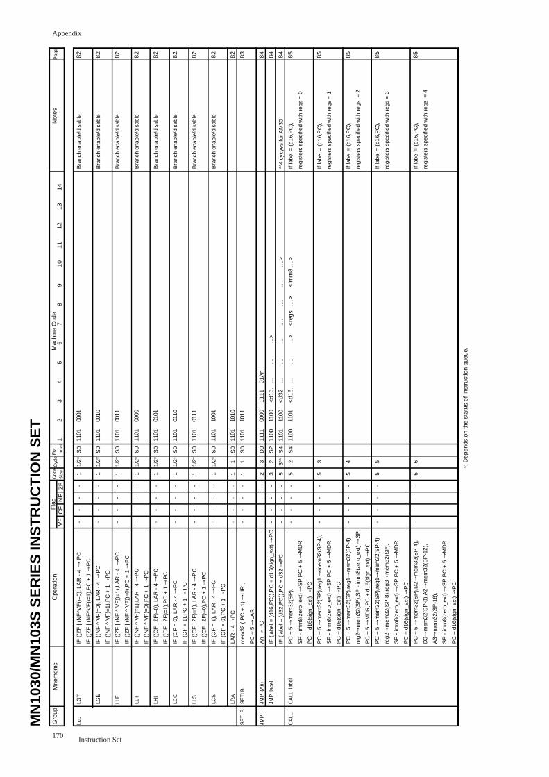
Appendix
170 Instruction Set
LGT�
� LGE
�
� LLE
�
� LLT�
� LHI�
� LCC
�
� LLS
�
� LCS
�
� LRA
�
SE
TLB
�
� JMP
(A
n)�
JMP
lab
el�
� CA
LL l
abel
IF (
(ZF
| (N
F^V
F))
=0)
, LA
R -
4 →
PC
�
IF (
(ZF
| (N
F^V
F))
=1)
,PC
+ 1
→P
C�
IF (
(NF
^ V
F)=
0), L
AR
- 4
→P
C�
IF (
(NF
^ V
F)=
1),P
C +
1 →
PC
�
IF (
(ZF
| (N
F ^
VF
))=
1),L
AR
- 4
→P
C�
IF (
(ZF
| (N
F ^
VF
))=
0),P
C +
1 →
PC
�
IF (
(NF
^ V
F)=
1),L
AR
- 4
→P
C�
IF (
(NF
^ V
F)=
0),P
C +
1 →
PC
�
IF (
(CF
| Z
F)=
0), L
AR
- 4
→P
C�
IF (
(CF
| Z
F)=
1),P
C +
1 →
PC
�
IF (
CF
= 0
), L
AR
- 4
→P
C�
IF (
CF
= 1
),P
C +
1 →
PC
�
IF (
(CF
| Z
F)=
1), L
AR
- 4
→P
C�
IF (
(CF
| Z
F)=
0),P
C +
1 →
PC
�
IF (
CF
= 1
), L
AR
- 4
→P
C�
IF (
CF
= 0
),P
C +
1 →
PC
�
LAR
- 4
→P
C�
�
mem
32 (
PC
+ 1
) →
LIR
, �
PC
+ 5
→LA
R�
An →
PC
�
IF (
labe
l = (
d16,
PC
)),P
C +
d16
(sig
n_ex
t) →
PC
�
IF (
labe
l = (
d32,
PC
)),P
C +
d32
→P
C�
PC
+ 5
→m
em32
(SP
),�
SP
- im
m8(
zero
_ext
) →
SP
,PC
+ 5
→M
DR
,�
PC
+ d
16(s
ign_
ext)
→P
C�
PC
+ 5
→m
em32
(SP
),re
g1 →
mem
32(S
P-4
),�
SP
- im
m8(
zero
_ext
) →
SP
,PC
+ 5
→M
DR
,�
PC
+ d
16(s
ign_
ext)
→P
C�
PC
+ 5
→m
em32
(SP
),re
g1→
mem
32(S
P-4
),�
reg2
→m
em32
(SP
),S
P -
imm
8(ze
ro_e
xt) →
SP
,�
PC
+ 5
→M
DR
,PC
+ d
16(s
ign_
ext)
→P
C�
PC
+ 5
→m
em32
(SP
),re
g1→
mem
32(S
P-4
),�
reg2
→m
em32
(SP
-8),
reg3
→m
em32
(SP
),�
SP
- im
m8(
zero
_ext
) →
SP
,PC
+ 5
→M
DR
,�
PC
+ d
16(s
ign_
ext)
→P
C�
PC
+ 5
→m
em32
(SP
),D
2→m
em32
(SP
-4),
�
D3→
mem
32(S
P-8
),A
2→m
em32
(SP
-12)
,�
A3→
mem
32(S
P-1
6),�
SP
- im
m8(
zero
_ext
) →
SP
,PC
+ 5
→M
DR
,�
PC
+ d
16(s
ign_
ext)
→P
C�
�
-� � -� � -� � -� � -� � -� � -� � -� � -� -� � -� -� -� -� � � -� � � -� � � -� � � � -
-� � -� � -� � -� � -� � -� � -� � -� � -� -� � -� -� -� -� � � -� � � -� � � -� � � � -
-� � -� � -� � -� � -� � -� � -� � -� � -� -� � -� -� -� -� � � -� � � -� � � -� � � � -
-� � -� � -� � -� � -� � -� � -� � -� � -� -� � -� -� -� -� � � -� � � -� � � -� � � � -
1� � 1� � 1� � 1� � 1� � 1� � 1� � 1� � 1� 1� � 2� 3� 5� 5� � � 5� � � 5� � � 5� � � � 5
1/2*
�
�
1/2*
�
�
1/2*
�
�
1/2*
�
�
1/2*
�
�
1/2*
�
�
1/2*
�
�
1/2*
�
� 1� 1� � 3� 2� 3**� 2� � � 3� � � 4� � � 5� � � � 6
S0� �
S0� �
S0� �
S0� �
S0� �
S0� �
S0� �
S0� �
S0�
S0� �
D0�
S2�
S4�
S4
1� � 1101
�
� 1101
�
� 1101
�
� 1101
�
� 1101
�
� 1101
�
� 1101
�
� 1101
�
� 1101
�
1101
�
� 1111
�
1100
�
1101
�
1100
�
�
2� � 0001
�
� 0010
�
� 0011
�
� 0000
�
� 0101
�
� 0110
�
� 0111
�
� 1001
�
� 1010
�
1011
�
� 0000
�
1100
�
1100
�
1101
3� � � � � � � � � � � � � � � � � � � � � 1111
�
<d1
6.�
<d3
2�
<d1
6.
4� � � � � � � � � � � � � � � � � � � � � 01A
n�
....�
....�
....
5� � � � � � � � � � � � � � � � � � � � � � ....�
....�
....�
�
6� � � � � � � � � � � � � � � � � � � � � � ....>
�
....�
....>
�
�
� �
Gro
up�
�
Mne
mon
icO
pera
tion
Mac
hine
Cod
eN
otes
Pag
eF
lag
Cod
e�
Siz
eC
ycle
For
�
-m
at
MN
1030
/MN
103S
SE
RIE
S IN
ST
RU
CT
ION
SE
T7� � � � � � � � � � � � � � � � � � � � � � � ...
.�
<re
gs
8� � � � � � � � � � � � � � � � � � � � � � � ....�
....>
9� � � � � � � � � � � � � � � � � � � � � � � ....�
<im
m8�
� �
10�
� � � � � � � � � � � � � � � � � � � � � � ....>
�
....>
11�
� �
12�
� �
1314
VF
CF
NF
ZF
� Lcc�
� � � � � � � � � � � � � � � � SE
TLB
�
� JMP
�
� � CA
LL�
�
�B
ranc
h en
able
/dis
able
�
� Bra
nch
enab
le/d
isab
le�
� Bra
nch
enab
le/d
isab
le�
� Bra
nch
enab
le/d
isab
le�
� Bra
nch
enab
le/d
isab
le�
� Bra
nch
enab
le/d
isab
le�
� Bra
nch
enab
le/d
isab
le�
� Bra
nch
enab
le/d
isab
le�
� � � � � � **4
cycy
es fo
r A
M30
�
If la
bel =
(d1
6,P
C),
�
regi
ster
s sp
ecifi
ed w
ith r
egs
= 0
�
� If la
bel =
(d1
6,P
C),
�
regi
ster
s sp
ecifi
ed w
ith r
egs
= 1
�
� If la
bel =
(d1
6,P
C),
�
regi
ster
s sp
ecifi
ed w
ith r
egs
= 2
�
� If la
bel =
(d1
6,P
C),
�
regi
ster
s sp
ecifi
ed w
ith r
egs
= 3
�
� � If la
bel =
(d1
6,P
C),
�
regi
ster
s sp
ecifi
ed w
ith r
egs
= 4
�
� � � � � �
*: D
epen
ds o
n th
e st
atus
of I
nstr
uctio
n qu
eue.
82� �
82� �
82� �
82� �
82� �
82� �
82� �
82� �
82�
83� �
84�
84�
84�
85� � �
85� � �
85� � �
85� � � �
85
�
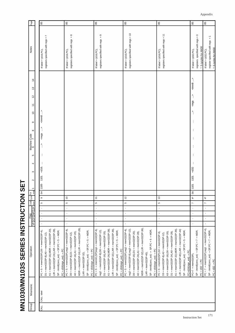
Appendix
171Instruction Set
CA
LL l
abel
PC
+ 5
→ m
em32
(SP
),D
0 →
mem
32(S
P-4
),�
D1→
mem
32(S
P-8
),A
0→ m
em32
(SP
-12)
,�
A1→
mem
32(S
P-1
6),M
DR→
mem
32(S
P-2
0),�
LIR→
mem
32(S
P-2
4),L
AR→
mem
32(S
P-2
8),�
SP
- im
m8(
zero
_ext
) →
SP
,PC
+ 5
→ M
DR
,�
PC
+ d
16(s
ign_
ext)
→ P
C�
PC
+ 5
→ m
em32
(SP
),re
g1→
mem
32(S
P-4
),�
D0→
mem
32(S
P-8
),D
1→ m
em32
(SP
-12)
,�
A0→
mem
32(S
P-1
6),A
1→ m
em32
(SP
-20)
,�
MD
R→
mem
32(S
P-2
4),L
IR→
mem
32(S
P-2
8),�
LAR→
mem
32(S
P-3
2),�
SP
- im
m8(
zero
_ext
) →
SP
,PC
+ 5
→ M
DR
,�
PC
+ d
16(s
ign_
ext)
→ P
C�
PC
+ 5
→ m
em32
,(S
P)r
eg1→
mem
32(S
P-4
),�
reg2
→ m
em32
(SP
-8),
D0→
mem
32(S
P-1
2),�
D1→
mem
32(S
P-1
6),A
0→ m
em32
(SP
-20)
,�
A1→
mem
32(S
P-2
4),M
DR→
mem
32(S
P-2
8),�
LIR→
mem
32(S
P-3
2),L
AR→
mem
32(S
P-3
6),�
SP
- im
m8(
zero
_ext
) →
SP
,PC
+ 5
→ M
DR
,�
PC
+ d
16(s
ign_
ext)
→ P
C�
PC
+ 5
→ m
em32
(SP
),re
g1→
mem
32(S
P-4
),�
reg2
→ m
em32
(SP
-8),
reg3
→ m
em32
(SP
-12)
,�
D0→
mem
32(S
P-1
6),D
1→ m
em32
(SP
-20)
,�
A0→
mem
32(S
P-2
4),A
1→ m
em32
(SP
-28)
,�
MD
R→
mem
32(S
P-3
2),L
IR→
mem
32(S
P-3
6),�
LAR→
mem
32(S
P-4
0),�
SP
- im
m8(
zero
_ext
) →
SP
,PC
+ 5
→ M
DR
,�
PC
+ d
16(s
ign_
ext)
→ P
C�
PC
+ 5
→m
em32
(SP
),D
2→ m
em32
(SP
-4),
�
D3→
mem
32(S
P-8
),A
2→ m
em32
(SP
-12)
,�
A3→
mem
32(S
P-1
6),D
0→ m
em32
(SP
-20)
,�
D1→
mem
32(S
P-2
4),A
0→ m
em32
(SP
-28)
,�
A1→
mem
32(S
P-3
2),M
DR→
mem
32(S
P-3
6),�
LIR→
mem
32(S
P-4
0),L
AR→
mem
32(S
P-4
4)�
SP
- im
m8(
zero
_ext
) →
SP
,PC
+ 5
→ M
DR
,�
PC
+d16
(sig
n_ex
t) →
PC
,�
PC
+7 →
mem
32(S
P),
�
SP
- im
m8(
zero
_ext
) →
SP
,PC
+ 7
→ M
DR
,�
PC
+ d
32 →
PC
�
PC
+ 7
→ m
em32
(SP
),re
g1 →
mem
32(S
P-4
),�
SP
- im
m8(
zero
_ext
) →
SP
,PC
+ 7
→ M
DR
,�
PC
+ d
32 →
PC
�
� �
Gro
up�
�
Mne
mon
icO
pera
tion
Not
esP
age
MN
1030
/MN
103S
SE
RIE
S IN
ST
RU
CT
ION
SE
T
CA
LL-� � � � � � -� � � � � � � -� � � � � � � -� � � � � � � � -� � � � � � � � -� � � -� �
-� � � � � � -� � � � � � � -� � � � � � � -� � � � � � � � -� � � � � � � � -� � � -� � �
-� � � � � � -� � � � � � � -� � � � � � � -� � � � � � � � -� � � � � � � � -� � � -� �
-� � � � � � -� � � � � � � -� � � � � � � -� � � � � � � � -� � � � � � � � -� � � -� � �
5� � � � � � 5� � � � � � � 5� � � � � � � 5� � � � � � � � 5� � � � � � � � 7� � � 7
9� � � � � � 10� � � � � � � 11� � � � � � � 12� � � � � � � � 13� � � � � � � � 4*� � � 4*
S4� � � � � � � � � � � � � � � � � � � � � � � � � � � � � � � � � � � �
S6
1� � 1100
�
� � � � � � � � � � � � � � � � � � � � � � � � � � � � � � � � � � � 1101
2� � 1101
�
� � � � � � � � � � � � � � � � � � � � � � � � � � � � � � � � � � � 1101
3� � <d16
. �
� � � � � � � � � � � � � � � � � � � � � � � � � � � � � � � � � � � <d32
�
�
4� � .... �
� � � � � � � � � � � � � � � � � � � � � � � � � � � � � � � � � � � ....
5� � .... �
� � � � � � � � � � � � � � � � � � � � � � � � � � � � � � � � � � � ....
6� � ....>
�
� � � � � � � � � � � � � � � � � � � � � � � � � � � � � � � � � � � ....�
�
� �
Mac
hine
Cod
eF
lag
Cod
e�
Siz
eC
ycle
For
�
-m
at7� � <r
egs
�
� � � � � � � � � � � � � � � � � � � � � � � � � � � � � � � � � � � ....
8� � ....>
�
� � � � � � � � � � � � � � � � � � � � � � � � � � � � � � � � � � � ....
9� � <im
m8
�
� � � � � � � � � � � � � � � � � � � � � � � � � � � � � � � � � � � ....�
�
10�
� ....>
�
� � � � � � � � � � � � � � � � � � � � � � � � � � � � � � � � � � � ....>
11�
�
� � � � � � � � � � � � � � � � � � � � � � � � � � � � � � � � � � � � <reg
s
12�
� � � � � � � � � � � � � � � � � � � � � � � � � � � � � � � � � � � � � ....>
13�
� � � � � � � � � � � � � � � � � � � � � � � � � � � � � � � � � � � � � <im
m8
14�
� � � � � � � � � � � � � � � � � � � � � � � � � � � � � � � � � � � � � ....>
VF
CF
NF
ZF
�If
labe
l = (
d16,
PC
),�
regi
ster
s sp
ecifi
ed w
ith r
egs
= 7�
� � � � If la
bel =
(d1
6,P
C),
�
regi
ster
s sp
ecifi
ed w
ith r
egs
= 8
�
� � � � � If la
bel =
(d1
6,P
C),
�
regi
ster
s sp
ecifi
ed w
ith r
egs
= 9
�
� � � � � If la
bel =
(d1
6,P
C),
�
regi
ster
s sp
ecifi
ied
with
reg
s =
10�
� � � � � � If la
bel =
(d1
6,P
C),
�
regi
ster
s sp
ecifi
ed w
ith r
egs
= 11
�
� � � � � � If la
bel =
(d3
2,P
C),
�
regi
ster
s s
peci
fied
with
reg
s =
0�
*: 5
cyc
yles
for
AM
30�
If la
bel =
(d3
2,P
C),
�
regi
ster
spe
cifie
d w
ith r
egs
= 1
�
*: 5
cyc
les
for
AM
30�
� � �
85� � � � � �
85� � � � � � �
85� � � � � � �
85� � � � � � � �
85� � � � � � � �
85� � �
85
�
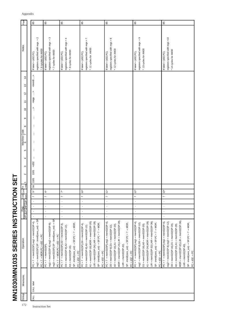
Appendix
172 Instruction Set
CA
LL l
abel
PC
+ 7
→ m
em32
(SP
),re
g1→
mem
32(S
P-4
),�
reg2
→ m
em32
(SP
),S
P -
imm
8(ze
ro_e
xt) →
SP
,�
PC
+ 7
→ M
DR
,PC
+ d
32 →
PC
�
PC
+ 7
→ m
em32
(SP
),�
reg1
→ m
em32
(SP
-4),
reg2
→ m
em32
(SP
-8),
�
reg3
→ m
em32
(SP
),S
P -
imm
8(ze
ro_e
xt) →
SP
,�
PC
+ 7
→ M
DR
,PC
+ d
32 →
PC
�
PC
+ 7
→ m
em32
(SP
),D
2→ m
em32
(SP
-4),
�
D3→
mem
32(S
P-8
),A
2→ m
em32
(SP
-12)
,�
A3→
mem
32(S
P-1
6),�
SP
- im
m8(
zero
_ext
) →
SP
,PC
+ 7
→ M
DR
,�
PC
+ d
32 →
PC
�
PC
+ 7
→ m
em32
(SP
),D
0→ m
em32
(SP
-4),
�
D1→
mem
32(S
P-8
),A
0→ m
em32
(SP
-12)
,�
A1→
mem
32(S
P-1
6),M
DR→
mem
32(S
P-2
0),�
LIR→
mem
32(S
P-2
4),L
AR→
mem
32(S
P-2
8),�
SP
- im
m8(
zero
_ext
) →
SP
,PC
+ 7
→ M
DR
,�
PC
+ d
32 →
PC
�
PC
+ 7
→ m
em32
(SP
),re
g1→
mem
32(S
P-4
),�
D0→
mem
32(S
P-8
),D
1→ m
em32
(SP
-12)
,�
A0→
mem
32(S
P-1
6),A
1→ m
em32
(SP
-20)
,�
MD
R→
mem
32(S
P-2
4),L
IR→
mem
32(S
P-2
8),�
LAR→
mem
32(S
P-3
2),�
SP
- im
m8(
zero
_ext
) →
SP
,PC
+ 7
→ M
DR
,�
PC
+ d
32 →
PC
�
PC
+ 7
→ m
em32
(SP
),re
g1→
mem
32(S
P-4
),�
reg2
→ m
em32
(SP
-8),
D0→
mem
32(S
P-1
2),�
D1→
mem
32(S
P-1
6),A
0→ m
em32
(SP
-20)
,�
A1→
mem
32(S
P-2
4),M
DR→
mem
32(S
P-2
8),�
LIR→
mem
32(S
P-3
2),L
AR→
mem
32(S
P-3
6),�
SP
- im
m8(
zero
_ext
) →
SP
,PC
+ 7
→ M
DR
,�
PC
+ d
32 →
PC
�
PC
+ 7
→ m
em32
(SP
),re
g1→
mem
32(S
P-4
),�
reg2
→ m
em32
(SP
-8),
reg3
→ m
em32
(SP
-12)
,�
D0→
mem
32(S
P-1
6),D
1→ m
em32
(SP
-20)
,�
A0→
mem
32(S
P-2
4),A
1→ m
em32
(SP
-28)
,�
MD
R→
mem
32(S
P-3
2),L
IR→
mem
32(S
P-3
6),�
LAR→
mem
32(S
P-4
0),�
SP
- im
m8(
zero
_ext
) →
SP
,PC
+ 7
→ M
DR
,�
PC
+ d
32 →
PC
�
�
-� � � -� � � � -� � � � � -� � � � � � -� � � � � � � -� � � � � � � -
-� � � -� � � � -� � � � � -� � � � � � -� � � � � � � -� � � � � � � -
-� � � -� � � � -� � � � � -� � � � � � -� � � � � � � -� � � � � � � -
-� � � -� � � � -� � � � � -� � � � � � -� � � � � � � -� � � � � � � -
7� � � 7� � � � 7� � � � � 7� � � � � � 7� � � � � � � 7� � � � � � � 7
5*� � � 6*� � � � 7*� � � � �
10*� � � � � �
11*� � � � � � �
12*� � � � � � �
13*
S6
1� � 1101
2� � 1101
3� � <d32
4� � ....
5� � ....
6� � ....
� �
Gro
up�
�
Mne
mon
icO
pera
tion
Mac
hine
Cod
eN
otes
Pag
eF
lag
Cod
e�
Siz
eC
ycle
For
�
-m
at
MN
1030
/MN
103S
SE
RIE
S IN
ST
RU
CT
ION
SE
T7� � ...
.
8� � ....
9� � ....
10�
� ....>
11�
� <reg
s
12�
� ....>
13�
� <im
m8
14�
� ....>
VF
CF
NF
ZF
CA
LL�
If la
bel =
(d3
2,P
C),
�
regi
ster
s sp
ecifi
ed w
ith r
egs
= 2
�
*: 6
cyc
yles
for
AM
30�
If la
bel =
(d3
2,P
C),
�
regi
ster
s sp
ecifi
ed w
tih r
egs
= 3
�
*: 7
cyc
les
for
AM
30 �
� If la
bel =
(d3
2,P
C),
�
regi
ster
s sp
ecifi
ed w
ith r
egs
= 4�
*: 8
cyc
les
for
AM
30�
� � If la
bel =
(d3
2,P
C),
�
regi
ster
s sp
ecifi
ed w
ith r
egs
= 7�
*: 1
1 cy
cles
for
AM
30�
� � � If la
bel =
(d3
2,P
C),
�
regi
ster
s sp
ecifi
ed w
ith r
egs
= 8�
*: 1
2 cy
cles
for
AM
30�
� � � � If la
bel =
(d3
2,P
C),
�
regi
ster
s sp
ecifi
ed w
ith r
egs
= 9
�
*: 1
3 cy
cles
for
AM
30�
� � � � If la
bel =
(d3
2,P
C),
�
regi
ster
s sp
ecifi
ed w
ith r
egs
=10�
* 14
cyc
les
for
AM
30�
� � � � � � �
85� � �
85� � � �
85� � � � �
85� � � � � �
85� � � � � � �
85� � � � � � �
85� � � � � � � �
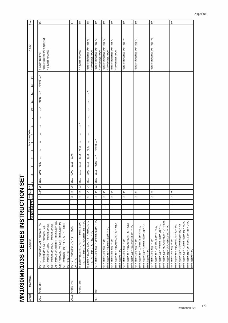
Appendix
173Instruction Set
CA
LL l
abel
�
� � � � � � � CA
LLS
(A
n)�
� CA
LLS
lab
el�
� � � RE
T
PC
+ 7
→ m
em32
(SP
),D
2→ m
em32
(SP
-4),
�
D3→
mem
32(S
P-8
),A
2→ m
em32
(SP
-12)
,�
A3→
mem
32(S
P-1
6),D
0→ m
em32
(SP
-20)
,�
D1→
mem
32(S
P-2
4),A
0→ m
em32
(SP
-28)
,�
A1→
mem
32(S
P-3
2),M
DR→
mem
32(S
P-3
6),�
LIR→
mem
32(S
P-4
0),L
AR→
mem
32(S
P-4
4)�
SP
- im
m8(
zero
_ext
) →
SP
,PC
+ 7
→ M
DR
,�
PC
+ d
32 →
PC
�
PC
+ 2
→ m
em32
(SP
),P
C +
2 →
MD
R,�
An →
PC
�
IF (
labe
l = (
d16,
PC
)), P
C +
4 →
mem
32(S
P),
�
P
C +
4 →
MD
R, P
C +
d16
(sig
n_ex
t) →
PC
�
IF (
(labe
l = (
d32,
PC
)), P
C +
6 →
mem
32(S
P),
�
P
C +
6 →
MD
R, P
C +
d32
→ P
C�
SP
+ im
m8(
zero
_ext
) →
SP
,mem
32(S
P) →
PC
�
� SP
+ im
m8(
zero
_ext
) →
SP
,�
mem
32(S
P-4
)→ r
eg, m
em32
(SP
) →
PC
�
SP
+ im
m8(
zero
_ext
) →
SP
,�
mem
32(S
P-4
)→ r
eg1,
mem
32(S
P-8
)→ r
eg2,
�
mem
32(S
P) →
PC
�
SP
+ im
m8(
zero
_ext
) →
SP
,�
mem
32(S
P-4
)→ r
eg1,
mem
32(S
P-8
)→ r
eg2,
�
mem
32(S
P-1
2)→
reg
3,m
em32
(SP
) →
PC
�
SP
+ im
m8(
zero
_ext
) →
SP
,�
mem
32(S
P-4
)→ D
2,m
em32
(SP
-8)→
D3,
�
mem
32(S
P-1
2)→
A2,
mem
32(S
P-1
6)→
A3,
�
mem
32(S
P) →
PC
�
SP
+ im
m8(
zero
_ext
) →
SP
,�
mem
32(S
P-4
)→ D
0,m
em32
(SP
-8)→
D1,
�
mem
32(S
P-1
2)→
A0,
mem
32(S
P-1
6)→
A1,
�
mem
32(S
P-2
0)→
MD
R,m
em32
(SP
-24)→
LIR
,�
mem
32(S
P-2
8)→
LA
R,m
em32
(SP
) →
PC
�
SP
+ im
m8(
zero
_ext
) →
SP
,�
mem
32(S
P-4
)→ r
eg1,
mem
32(S
P-8
)→ D
0,�
mem
32(S
P-1
2)→
D1,
mem
32(S
P-1
6)→
A0,
�
mem
32(S
P-2
0)→
A1,
mem
32(S
P-2
4)→
MD
R,�
mem
32(S
P-2
8)→
LIR
,mem
32(S
P-3
2)→
LA
R,�
mem
32(S
P) →
PC
�
�
-� � � � � � � � -� � -� � -� � -� � -� � -� � � -� � � -� � � � -� � � � � -
-� � � � � � � � -� � -� � -� � -� � -� � -� � � -� � � -� � � � -� � � � � -
-� � � � � � � � -� � -� � -� � -� � -� � -� � � -� � � -� � � � -� � � � � -
-� � � � � � � � -� � -� � -� � -� � -� � -� � � -� � � -� � � � -� � � � � -
7� � � � � � � � 2� � 4� � 6� � 3� � 3� � 3� � � 3� � � 3� � � � 3� � � � � 3
14*� � � � � � � � 3� � 3� � 3*� � 5*� � 5*� � 5*� � � 5*� � � 5� � � � 8� � � � � 9� � � � �
S6� � � � � � � �
D0� �
D2� �
D4� �
S2
1� � 1101
�
� � � � � � � 1111
�
� 1111
�
� 1111
�
� 1101
2� � 1101
�
� � � � � � � 0000
�
� 1010
�
� 1100
�
� 1111
3� � <d3
2�
� � � � � � � 1111
�
� 1111
�
� 1111
�
� <re
gs
4� � ....�
� � � � � � � 00A
n�
� 1111
�
� 1111
�
� ....>
5� � ....�
� � � � � � � � � <d1
6�
� <d3
2�
� <im
m8
6� � ....�
� � � � � � � � � ....�
� ....�
� ....>
� �
Gro
up�
�
Mne
mon
icO
pera
tion
Mac
hine
Cod
eN
otes
Pag
eF
lag
Cod
e�
Siz
eC
ycle
For
�
-m
at
MN
1030
/MN
103S
SE
RIE
S IN
ST
RU
CT
ION
SE
T7� � ...
.�
� � � � � � � � � ....�
� ....
8� � ....�
� � � � � � � � � ....>
�
� ....�
�
9� � ....�
� � � � � � � � � � � ....
10�
� ....>
�
� � � � � � � � � � � ....
11�
� <re
gs�
� � � � � � � � � � � ....
12�
� ....>
�
� � � � � � � � � � � ....>
13�
� <im
m8
14�
� ....>
VF
CF
NF
ZF
CA
LL�
� � � � � � � CA
LLS
�
� � � � � RE
T
��
If la
bel =
(d3
2,P
C),
�
regi
ster
sspe
cifie
d w
ith r
egs
=11
�
*: 5
cyc
les
for
AM
30�
� � � � � � � *: 4
cyc
les
for
AM
30�
� regi
ster
s sp
ecifi
ed w
ith r
egs
=0�
*:4
cycl
es fo
r A
M30
�
regi
ster
s sp
ecifi
ed w
ith r
egs
=1�
*:4
cycl
es fo
r A
M30
�
regi
ster
s sp
ecifi
ed w
ith r
egs
=2�
*:4
cycl
es fo
r A
M30
�
regi
ster
s sp
ecifi
ed w
ith r
egs
=3�
*:4
cycl
es fo
r A
M30
�
� regi
ster
s sp
ecifi
ed w
ith r
egs
=4�
� � regi
ster
s sp
ecifi
ed w
ith r
egs
=7�
� � � regi
ster
s sp
ecifi
ed w
ith r
egs
=8�
�
85� � � � � � � �
87� �
88� �
88� �
89� �
89� �
89� � �
89� � �
89� � � �
89� � � � �
89� � �
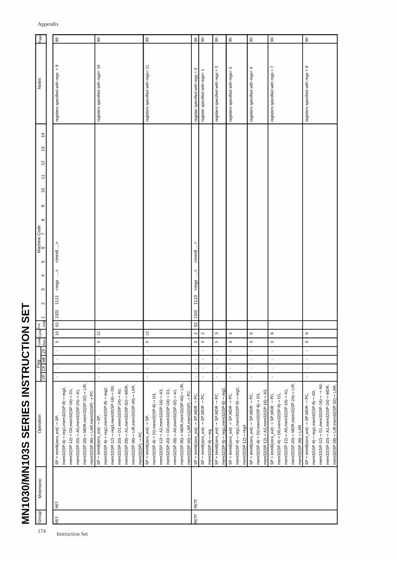
Appendix
174 Instruction Set
RE
T�
� � � � � � � � � � � � � � � � � � � RE
TF
SP
+ im
m8(
zero
_ext
) →
SP
,�
mem
32(S
P-4
)→ r
eg1,
mem
32(S
P-8
)→ r
eg2,
�
mem
32(S
P-1
2)→
D0,
mem
32(S
P-1
6)→
D1,
�
mem
32(S
P-2
0)→
A0,
mem
32(S
P-2
4)→
A1,
�
mem
32(S
P-2
8)→
MD
R,m
em32
(SP
-32)→
LIR
,�
mem
32(S
P-3
6)→
LA
R,m
em32
(SP
) →
PC
�
SP
+ im
m8(
zero
_ext
) →
SP
,�
mem
32(S
P-4
)→ r
eg1,
mem
32(S
P-8
)→ r
eg2,
�
mem
32(S
P-1
2)→
reg
3,m
em32
(SP
-16)→
D0,
�
mem
32(S
P-2
0)→
D1,
mem
32(S
P-2
4)→
A0,
�
mem
32(S
P-2
8)→
A1,
mem
32(S
P-3
2)→
MD
R,�
mem
32(S
P-3
6)→
LIR
,mem
32(S
P-4
0)→
LA
R,�
mem
32(S
P) →
PC
�
SP
+ im
m8(
zero
_ext
) →
SP
,�
mem
32(S
P-4
)→ D
2,m
em32
(SP
-8)→
D3,
�
mem
32(S
P-1
2)→
A2,
mem
32(S
P-1
6)→
A3,
�
mem
32(S
P-2
0)→
D0,
mem
32(S
P-2
4)→
D1,
�
mem
32(S
P-2
8)→
A0,
mem
32(S
P-3
2)→
A1,
�
mem
32(S
P-3
6)→
MD
R,m
em32
(SP
-40)→
LIR
,�
mem
32(S
P-4
4)→
LA
R,m
em32
(SP
) →
PC
�
SP
+ im
m8(
zero
_ext
) →
SP
,MD
R →
PC
,�
SP
+ im
m8(
zero
_ext
) →
SP
,MD
R →
PC
,�
mem
32(S
P-4
)→ r
eg�
SP
+ im
m8(
zero
_ext
) →
SP
,MD
R →
PC
,�
mem
32(S
P-4
)→ r
eg1,
mem
32(S
P-8
)→ r
eg2,
�
SP
+ im
m8(
zero
_ext
) →
SP
,MD
R →
PC
,�
mem
32(S
P-4
)→ r
eg1,
mem
32(S
P-8
)→ r
eg2,
�
mem
32(S
P-1
2)→
reg
3�
SP
+ im
m8(
zero
_ext
) →
SP
,MD
R →
PC
,�
mem
32(S
P-4
)→ D
2,m
em32
(SP
-8)→
D3,
�
mem
32(S
P-1
2)→
A2,
mem
32(S
P-1
6)→
A3,
�
SP
+ im
m8(
zero
_ext
) →
SP
,MD
R →
PC
,�
mem
32(S
P-4
)→ D
0,m
em32
(SP
-8)→
D1,
�
mem
32(S
P-1
2)→
A0,
mem
32(S
P-1
6)→
A1,
�
mem
32(S
P-2
0)→
MD
R,m
em32
(SP
-24)→
LIR
,�
mem
32(S
P-2
8)→
LA
R�
SP
+ im
m8(
zero
_ext
) →
SP
,MD
R →
PC
,�
mem
32(S
P-4
)→ r
eg1,
mem
32(S
P-8
)→ D
0,�
mem
32(S
P-1
2)→
D1,
mem
32(S
P-1
6)→
→ A
0,�
mem
32(S
P-2
0)→
A1,
mem
32(S
P-2
4)→
MD
R,�
mem
32(S
P-2
8)→
LIR
,mem
32(S
P-3
2)→
LA
R,�
�
-� � � � � � -� � � � � � � -� � � � � � � -� -� � -� � -� � � -� � � -� � � � � -
-� � � � � � -� � � � � � � -� � � � � � � -� -� � -� � -� � � -� � � -� � � � � -
-� � � � � � -� � � � � � � -� � � � � � � -� -� � -� � -� � � -� � � -� � � � � -
-� � � � � � -� � � � � � � -� � � � � � � -� -� � -� � -� � � -� � � -� � � � � -
3� � � � � � 3� � � � � � � 3� � � � � � � 3� 3� � 3� � 3� � � 3� � � 3� � � � � 3
10� � � � � � 11� � � � � � � 12� � � � � � � 2� 2� � 3� � 4� � � 5� � � 8� � � � � 9
S2� � � � � � � � � � � � � � � � � � � �
S2
1� � 1101
�
� � � � � � � � � � � � � � � � � � � 1101
2� � 1111
�
� � � � � � � � � � � � � � � � � � � 1110
3� � <re
gs�
� � � � � � � � � � � � � � � � � � � <re
gs
4� � ....>
�
� � � � � � � � � � � � � � � � � � � ....>
5� � <im
m8�
� � � � � � � � � � � � � � � � � � � <im
m8
6� � ....>
�
� � � � � � � � � � � � � � � � � � � ....>
� �
Gro
up�
�
Mne
mon
icO
pera
tion
Mac
hine
Cod
eN
otes
Pag
eF
lag
Cod
e�
Siz
eC
ycle
For
�
-m
at
MN
1030
/MN
103S
SE
RIE
S IN
ST
RU
CT
ION
SE
T7� � �
8� � �
9� � �
10�
� �
11�
� �
12�
�
1314
VF
CF
NF
ZF
RE
T�
� � � � � � � � � � � � � � � � � � � RE
TF
�re
gist
ers
spec
ified
with
reg
s =
9�
� � � � � regi
ster
s sp
ecifi
ed w
ith r
egs=
10�
� � � � � � regi
ster
s sp
ecifi
ed w
ith r
egs=
11�
� � � � � � regi
ster
spe
cifie
d w
ith r
egs
= 0
�
regi
ster
spe
cifie
d w
ith r
egs=
1�
� regi
ster
s sp
ecifi
ed w
ith r
egs
= 2
�
� regi
ster
s sp
ecifi
ed w
ith r
egs=
3�
� � regi
ster
s sp
ecifi
ed w
ith r
egs=
4�
� � regi
ster
s sp
ecifi
ed w
ith r
egs
= 7
�
� � � � regi
ster
s sp
ecifi
ed w
ith r
egs
= 8
�
89� � � � � �
89� � � � � � �
89� � � � � � �
90�
90� �
90� �
90� � �
90� � �
90� � � � �
90
Appendix
175Instruction Set
RE
TF�
� � � � � � � � � � � � � � � � � � RE
TS�
JSR
(A
n)�
� � � JSR
lab
el�
� � � � � � � � � RTS
�
RTI
�
� TRA
P�
NO
P�
�
SP
+ im
m8(
zero
_ext
) →
SP
,MD
R →
PC
,�
mem
32(S
P-4
)→ r
eg1,
mem
32(S
P-8
)→ r
eg2,
�
mem
32(S
P-1
2)→
D0,
mem
32(S
P-1
6)→
D1,
�
mem
32(S
P-2
0)→
A0,
mem
32(S
P-2
4)→
A1,
�
mem
32(S
P-2
8)→
MD
R,m
em32
(SP
-32)→
LIR
,�
mem
32(S
P-3
6)→
LA
R�
SP
+ im
m8(
zero
_ext
) →
SP
,MD
R →
PC
,�
mem
32(S
P-4
)→ r
eg1,
mem
32(S
P-8
)→ r
eg2,
�
mem
32(S
P-1
2)→
reg
3,m
em32
(SP
-16)→
D0,
�
mem
32(S
P-2
0)→
D1,
mem
32(S
P-2
4)→
A0,
�
mem
32(S
P-2
8)→
A1,
mem
32(S
P-3
2)→
MD
R,�
mem
32(S
P-3
6)→
LIR
,mem
32(S
P-4
0)→
LA
R,�
SP
+ im
m8(
zero
_ext
) →
SP
,MD
R →
PC
,�
mem
32(S
P-4
)→ D
2,m
em32
(SP
-8)→
D3,
�
mem
32(S
P-1
2)→
A2,
mem
32(S
P-1
6)→
A3,
�
mem
32(S
P-2
0)→
D0,
mem
32(S
P-2
4)→
D1,
�
mem
32(S
P-2
8)→
A0,
mem
32(S
P-3
2)→
A1,
�
mem
32(S
P-3
6)→
MD
R,m
em32
(SP
-40)→
LIR
,�
mem
32(S
P-4
4)→
LA
R�
mem
32(S
P) →
PC
�
SP
- 4
→ S
P,P
C +
2 →
mem
32(S
P)�
PC
+ 2
→ M
DR
,An →
PC
,�
(exe
cute
sub
rout
ine)
�
SP
+ 4
→ S
P�
IF (
labe
l = (
d16,
PC
)),�
SP
- 4
→ S
P,P
C +
4 →
mem
32(S
P),
�
PC
+ 4
→ M
DR
,PC
+ d
16 (
sign
_ext
) →
PC
�
(exe
cute
sub
rout
ine)
�
SP
+4 →
SP
�
IF (
labe
l = (
d32,
PC
)),�
SP
- 4
→ S
P,P
C +
6 →
(S
P+
3),�
PC
+ 6
→ M
DR
,PC
+ d
32 →
PC
�
(exe
cute
sub
rout
ine)
�
SP
+4 →
SP
�
mem
32(S
P) →
PC
�
mem
16(S
P)
→ P
SW
,mem
32(S
P+
4) →
PC
,�
SP
+ 8
→ S
P�
PC
+ 2
→ m
em32
(SP
),0x
4000
0010
→ P
C�
PC
+ 1
→ P
C�
� �
-� � � � � � -� � � � � � -� � � � � � � -� ● ● ● - ● � -� -
-� � � � � � -� � � � � � -� � � � � � � -� ● ● ● - ● � -� -
-� � � � � � -� � � � � � -� � � � � � � -� ● ● ● -� ● � -� -
-� � � � � � -� � � � � � -� � � � � � � -� ● ● ● - ● � -� -
3� � � � � � 3� � � � � � 3� � � � � � � 2� 8� � � � 10� � � � � 12� � � � � 2� 2� � 2� 1� � �
10� � � � � � 11� � � � � � 10� � � � � � � 5*�
5� � � � 5� � � � � 5*� � � � � 4� 4� � 4� 1
S2� � � � � � � � � � � � � � � � � � �
D0� � � � � � � � � � � � � � �
D0� � �
D0�
S0� � �
1� � 1101
�
� � � � � � � � � � � � � � � � � � 1111
�
� � � � � � � � � � � � � � 1111
�
� � 1111
�
1100
�
�
2� � 1110
�
� � � � � � � � � � � � � � � � � � 0000
�
� � � � � � � � � � � � � � 0000
�
� � 0000
�
1011
�
�
3� � <re
gs�
� � � � � � � � � � � � � � � � � � 1111
�
� � � � � � � � � � � � � � 1111
�
� � 1111
�
� �
4� � ....>
�
� � � � � � � � � � � � � � � � � � 1100
�
� � � � � � � � � � � � � � 1101
�
� � 1110
�
�
5� � <im
m8
6� � ....>
� �
Gro
up�
�
Mne
mon
icO
pera
tion
Mac
hine
Cod
eN
otes
Pag
eF
lag
Cod
e�
Siz
eC
ycle
For
�
-m
at
MN
1030
/MN
103S
SE
RIE
S IN
ST
RU
CT
ION
SE
T7� � �
8� � �
9� � �
10�
� �
11�
�
12�
�
1314
VF
CF
NF
ZF
RE
TF�
� � � � � � � � � � � � � � � � � � RE
TS�
JSR
�
� � � � � � � � � � � � � RTS
�
RTI
�
� TRA
P�
NO
P�
�
�re
gist
ers
spec
ified
with
reg
s =
9�
� � � � � regi
ster
s sp
ecifi
ed w
ith r
egs=
10�
� � � � � regi
ster
s sp
ecifi
ed w
ith r
egs=
11�
� � � � � � *: 4
cyc
les
for
AM
30�
� � � � � � � � � *: 6
cyc
les
for
AM
30
90� � � � � �
90� � � � � �
90� � � � � � �
91�
92� � � �
93� � � � �
93� � � � �
94�
95� �
96�
97
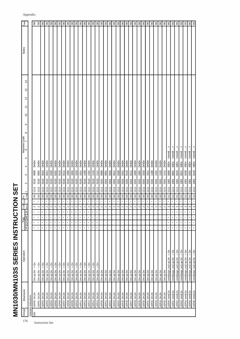
Appendix
176 Instruction Set
UD
F00
Dm
,Dn�
UD
F01
Dm
,Dn�
UD
F02
Dm
,Dn�
UD
F03
Dm
,Dn�
UD
F04
Dm
,Dn�
UD
F05
Dm
,Dn�
UD
F06
Dm
,Dn�
UD
F07
Dm
,Dn�
UD
F08
Dm
,Dn�
UD
F09
Dm
,Dn�
UD
F10
Dm
,Dn�
UD
F11
Dm
,Dn�
UD
F12
Dm
,Dn�
UD
F13
Dm
,Dn�
UD
F14
Dm
,Dn�
UD
F15
Dm
,Dn�
UD
F20
Dm
,Dn�
UD
F21
Dm
,Dn�
UD
F22
Dm
,Dn�
UD
F23
Dm
,Dn�
UD
F24
Dm
,Dn�
UD
F25
Dm
,Dn�
UD
F26
Dm
,Dn�
UD
F27
Dm
,Dn�
UD
F28
Dm
,Dn�
UD
F29
Dm
,Dn�
UD
F30
Dm
,Dn�
UD
F31
Dm
,Dn�
UD
F32
Dm
,Dn�
UD
F33
Dm
,Dn�
UD
F34
Dm
,Dn�
UD
F35
Dm
,Dn�
UD
F00
imm
8,D
n�
UD
F01
imm
8,D
n�
UD
F02
imm
8,D
n�
UD
F03
imm
8,D
n�
UD
F04
imm
8,D
n�
UD
F05
imm
8,D
n�
UD
F06
imm
8,D
n
Dm
op
Dn
→ D
n �
Dm
op
Dn
→ D
n �
Dm
op
Dn
→ D
n �
Dm
op
Dn
→ D
n �
Dm
op
Dn
→ D
n �
Dm
op
Dn
→ D
n �
Dm
op
Dn
→ D
n �
Dm
op
Dn
→ D
n �
Dm
op
Dn
→ D
n �
Dm
op
Dn
→ D
n �
Dm
op
Dn
→ D
n �
Dm
op
Dn
→ D
n �
Dm
op
Dn
→ D
n �
Dm
op
Dn
→ D
n �
Dm
op
Dn
→ D
n �
Dm
op
Dn
→ D
n �
Dm
op
Dn�
Dm
op
Dn�
Dm
op
Dn�
Dm
op
Dn�
Dm
op
Dn�
Dm
op
Dn�
Dm
op
Dn�
Dm
op
Dn�
Dm
op
Dn�
Dm
op
Dn�
Dm
op
Dn�
Dm
op
Dn�
Dm
op
Dn�
Dm
op
Dn�
Dm
op
Dn�
Dm
op
Dn�
imm
8(si
gn_e
xt)
op D
n →
Dn
�
imm
8(si
gn_e
xt)
op D
n →
Dn�
imm
8(si
gn_e
xt)
op D
n →
Dn�
imm
8(si
gn_e
xt)
op D
n →
Dn�
imm
8(si
gn_e
xt)
op D
n →
Dn�
imm
8(si
gn_e
xt)
op D
n →
Dn�
imm
8(si
gn_e
xt)
op D
n →
Dn
*� *� *� *� *� *� *� *� *� *� *� *� *� *� *� *� -� -� -� -� -� -� -� -� -� -� -� -� -� -� -� -� *� *� *� *� *� *� *
*� *� *� *� *� *� *� *� *� *� *� *� *� *� *� *� -� -� -� -� -� -� -� -� -� -� -� -� -� -� -� -� *� *� *� *� *� *� *
*� *� *� *� *� *� *� *� *� *� *� *� *� *� *� *� -� -� -� -� -� -� -� -� -� -� -� -� -� -� -� -� *� *� *� *� *� *� *
*� *� *� *� *� *� *� *� *� *� *� *� *� *� *� *� -� -� -� -� -� -� -� -� -� -� -� -� -� -� -� -� *� *� *� *� *� *� *
2� 2� 2� 2� 2� 2� 2� 2� 2� 2� 2� 2� 2� 2� 2� 2� 2� 2� 2� 2� 2� 2� 2� 2� 2� 2� 2� 2� 2� 2� 2� 2� 3� 3� 3� 3� 3� 3� 3
*� *� *� *� *� *� *� *� *� *� *� *� *� *� *� *� *� *� *� *� *� *� *� *� *� *� *� *� *� *� *� *� *� *� *� *� *� *� *
D0�
D0�
D0�
D0�
D0�
D0�
D0�
D0�
D0�
D0�
D0�
D0�
D0�
D0�
D0�
D0�
D0�
D0�
D0�
D0�
D0�
D0�
D0�
D0�
D0�
D0�
D0�
D0�
D0�
D0�
D0�
D0�
D1�
D1�
D1�
D1�
D1�
D1�
D1
1� � 1111
�
1111
�
1111
�
1111
�
1111
�
1111
�
1111
�
1111
�
1111
�
1111
�
1111
�
1111
�
1111
�
1111
�
1111
�
1111
�
1111
�
1111
�
1111
�
1111
�
1111
�
1111
�
1111
�
1111
�
1111
�
1111
�
1111
�
1111
�
1111
�
1111
�
1111
�
1111
�
1111
�
1111
�
1111
�
1111
�
1111
�
1111
�
1111
�
� �
2� � 0110
�
0110
�
0110
�
0110
�
0110
�
0110
�
0110
�
0110
�
0110
�
0110
�
0110
�
0110
�
0110
�
0110
�
0110
�
0110
�
0101
�
0101
�
0101
�
0101
�
0101
�
0101
�
0101
�
0101
�
0101
�
0101
�
0101
�
0101
�
0101
�
0101
�
0101
�
0101
�
1001
�
1001
�
1001
�
1001
�
1001
�
1001
�
1001
3� � 0000
�
0001
�
0010
�
0011
�
0100
�
0101
�
0110
�
0111
�
1000
�
1001
�
1010
�
1011
�
1100
�
1101
�
1110
�
1111
�
0000
�
0001
�
0010
�
0011
�
0100
�
0101
�
0110
�
0111
�
1000
�
1001
�
1010
�
1011
�
1100
�
1101
�
1110
�
1111
�
0000
�
0001
�
0010
�
0011
�
0100
�
0101
�
0110
4� � Dm
Dn�
Dm
Dn�
Dm
Dn�
Dm
Dn�
Dm
Dn�
Dm
Dn�
Dm
Dn�
Dm
Dn�
Dm
Dn�
Dm
Dn�
Dm
Dn�
Dm
Dn�
Dm
Dn�
Dm
Dn�
Dm
Dn�
Dm
Dn�
Dm
Dn�
Dm
Dn�
Dm
Dn�
Dm
Dn�
Dm
Dn�
Dm
Dn�
Dm
Dn�
Dm
Dn�
Dm
Dn�
Dm
Dn�
Dm
Dn�
Dm
Dn�
Dm
Dn�
Dm
Dn�
Dm
Dn�
Dm
Dn�
00D
n�
00D
n�
00D
n�
00D
n�
00D
n�
00D
n�
00D
n
5� � � � � � � � � � � � � � � � � � � � � � � � � � � � � � � � � � <im
m8�
<im
m8�
<im
m8�
<im
m8�
<im
m8�
<im
m8�
<im
m8
6� � � � � � � � � � � � � � � � � � � � � � � � � � � � � � � � � � ....>
�
....>
�
....>
�
....>
�
....>
�
....>
�
....>
�
�
� �
Gro
up�
�
Mne
mon
icO
pera
tion
Mac
hine
Cod
eN
otes
Pag
eF
lag
Cod
e�
Siz
eC
ycle
For
�
-m
at
MN
1030
/MN
103S
SE
RIE
S IN
ST
RU
CT
ION
SE
T7� � �
8� � �
9� � �
10�
� �
11�
�
12�
�
1314
VF
CF
NF
ZF
Ext
ensi
on In
stru
ctio
ns�
UD
F�
�
�
98�
98�
98�
98�
98�
98�
98�
98�
98�
98�
98�
98�
98�
98�
98�
98�
98�
98�
98�
98�
98�
98�
98�
98�
98�
98�
98�
98�
98�
98�
98�
98�
99�
99�
99�
99�
99�
99�
99
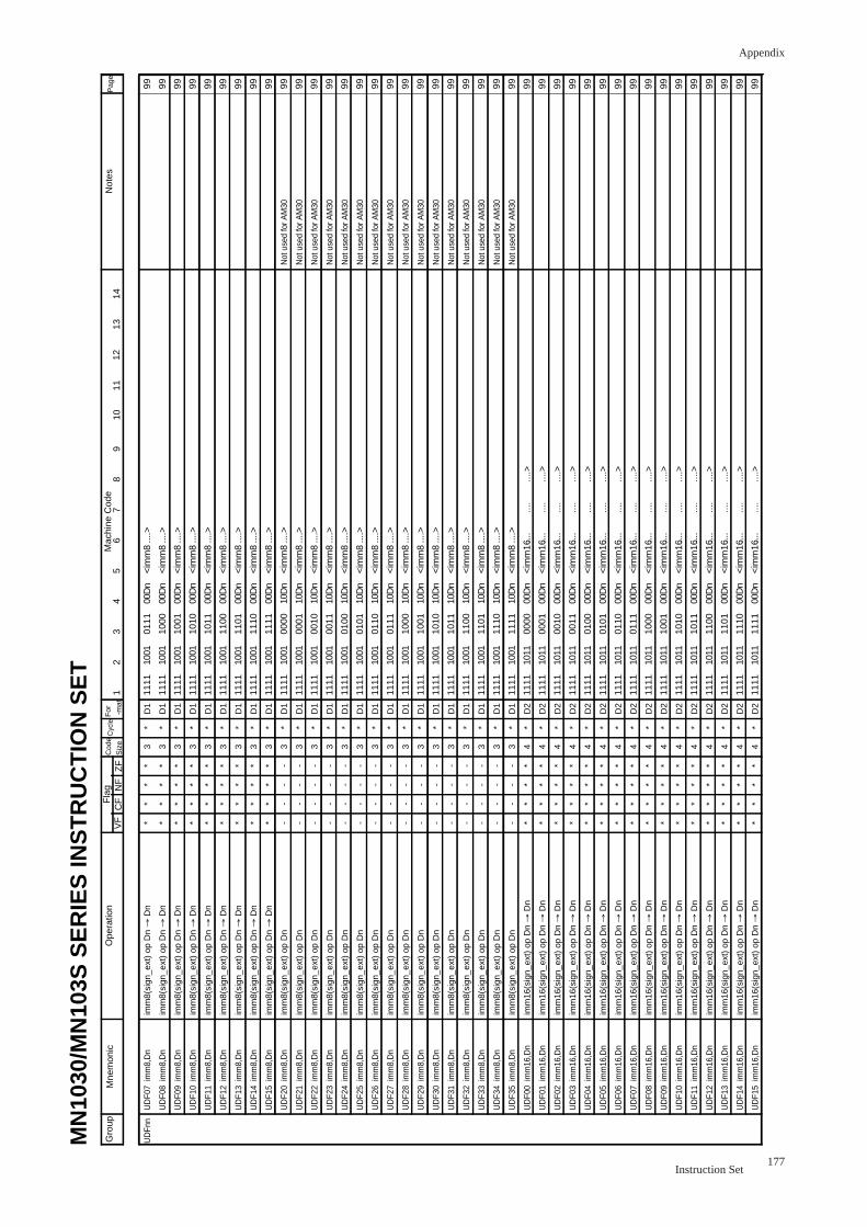
Appendix
177Instruction Set
UD
F07
imm
8,D
n�
UD
F08
imm
8,D
n�
UD
F09
imm
8,D
n�
UD
F10
imm
8,D
n�
UD
F11
imm
8,D
n�
UD
F12
imm
8,D
n�
UD
F13
imm
8,D
n�
UD
F14
imm
8,D
n�
UD
F15
imm
8,D
n�
UD
F20
imm
8,D
n�
UD
F21
imm
8,D
n�
UD
F22
imm
8,D
n�
UD
F23
imm
8,D
n�
UD
F24
imm
8,D
n�
UD
F25
imm
8,D
n�
UD
F26
imm
8,D
n�
UD
F27
imm
8,D
n�
UD
F28
imm
8,D
n�
UD
F29
imm
8,D
n�
UD
F30
imm
8,D
n�
UD
F31
imm
8,D
n�
UD
F32
imm
8,D
n�
UD
F33
imm
8,D
n�
UD
F34
imm
8,D
n�
UD
F35
imm
8,D
n�
UD
F00
imm
16,D
n�
UD
F01
imm
16,D
n�
UD
F02
imm
16,D
n�
UD
F03
imm
16,D
n�
UD
F04
imm
16,D
n�
UD
F05
imm
16,D
n�
UD
F06
imm
16,D
n�
UD
F07
imm
16,D
n�
UD
F08
imm
16,D
n�
UD
F09
imm
16,D
n�
UD
F10
imm
16,D
n�
UD
F11
imm
16,D
n�
UD
F12
imm
16,D
n�
UD
F13
imm
16,D
n�
UD
F14
imm
16,D
n�
UD
F15
imm
16,D
n�
�
imm
8(si
gn_e
xt)
op D
n →
Dn
�
imm
8(si
gn_e
xt)
op D
n →
Dn
�
imm
8(si
gn_e
xt)
op D
n →
Dn
�
imm
8(si
gn_e
xt)
op D
n →
Dn
�
imm
8(si
gn_e
xt)
op D
n →
Dn
�
imm
8(si
gn_e
xt)
op D
n →
Dn
�
imm
8(si
gn_e
xt)
op D
n →
Dn
�
imm
8(si
gn_e
xt)
op D
n →
Dn
�
imm
8(si
gn_e
xt)
op D
n →
Dn
�
imm
8(si
gn_e
xt)
op D
n �
imm
8(si
gn_e
xt)
op D
n �
imm
8(si
gn_e
xt)
op D
n �
imm
8(si
gn_e
xt)
op D
n�
imm
8(si
gn_e
xt)
op D
n�
imm
8(si
gn_e
xt)
op D
n�
imm
8(si
gn_e
xt)
op D
n�
imm
8(si
gn_e
xt)
op D
n�
imm
8(si
gn_e
xt)
op D
n�
imm
8(si
gn_e
xt)
op D
n�
imm
8(si
gn_e
xt)
op D
n�
imm
8(si
gn_e
xt)
op D
n�
imm
8(si
gn_e
xt)
op D
n�
imm
8(si
gn_e
xt)
op D
n�
imm
8(si
gn_e
xt)
op D
n�
imm
8(si
gn_e
xt)
op D
n�
imm
16(s
ign_
ext)
op
Dn →
Dn�
imm
16(s
ign_
ext)
op
Dn →
Dn�
imm
16(s
ign_
ext)
op
Dn →
Dn�
imm
16(s
ign_
ext)
op
Dn →
Dn�
imm
16(s
ign_
ext)
op
Dn →
Dn�
imm
16(s
ign_
ext)
op
Dn →
Dn�
imm
16(s
ign_
ext)
op
Dn →
Dn�
imm
16(s
ign_
ext)
op
Dn →
Dn�
imm
16(s
ign_
ext)
op
Dn →
Dn�
imm
16(s
ign_
ext)
op
Dn →
Dn�
imm
16(s
ign_
ext)
op
Dn →
Dn�
imm
16(s
ign_
ext)
op
Dn →
Dn�
imm
16(s
ign_
ext)
op
Dn →
Dn�
imm
16(s
ign_
ext)
op
Dn →
Dn�
imm
16(s
ign_
ext)
op
Dn →
Dn�
imm
16(s
ign_
ext)
op
Dn →
Dn�
�
*� *� *� *� *� *� *� *� *� -� -� -� -� -� -� -� -� -� -� -� -� -� -� -� -� *� *� *� *� *� *� *� *� *� *� *� *� *� *� *� *
*� *� *� *� *� *� *� *� *� -� -� -� -� -� -� -� -� -� -� -� -� -� -� -� -� *� *� *� *� *� *� *� *� *� *� *� *� *� *� *� *
*� *� *� *� *� *� *� *� *� -� -� -� -� -� -� -� -� -� -� -� -� -� -� -� -� *� *� *� *� *� *� *� *� *� *� *� *� *� *� *� *
*� *� *� *� *� *� *� *� *� -� -� -� -� -� -� -� -� -� -� -� -� -� -� -� -� *� *� *� *� *� *� *� *� *� *� *� *� *� *� *� *
3� 3� 3� 3� 3� 3� 3� 3� 3� 3� 3� 3� 3� 3� 3� 3� 3� 3� 3� 3� 3� 3� 3� 3� 3� 4� 4� 4� 4� 4� 4� 4� 4� 4� 4� 4� 4� 4� 4� 4� 4
*� *� *� *� *� *� *� *� *� *� *� *� *� *� *� *� *� *� *� *� *� *� *� *� *� *� *� *� *� *� *� *� *� *� *� *� *� *� *� *� *
D1�
D1�
D1�
D1�
D1�
D1�
D1�
D1�
D1�
D1�
D1�
D1�
D1�
D1�
D1�
D1�
D1�
D1�
D1�
D1�
D1�
D1�
D1�
D1�
D1�
D2�
D2�
D2�
D2�
D2�
D2�
D2�
D2�
D2�
D2�
D2�
D2�
D2�
D2�
D2�
D2
1� � 1111
�
1111
�
1111
�
1111
�
1111
�
1111
�
1111
�
1111
�
1111
�
1111
�
1111
�
1111
�
1111
�
1111
�
1111
�
1111
�
1111
�
1111
�
1111
�
1111
�
1111
�
1111
�
1111
�
1111
�
1111
�
1111
�
1111
�
1111
�
1111
�
1111
�
1111
�
1111
�
1111
�
1111
�
1111
�
1111
�
1111
�
1111
�
1111
�
1111
�
1111
�
�
2� � 1001
�
1001
�
1001
�
1001
�
1001
�
1001
�
1001
�
1001
�
1001
�
1001
�
1001
�
1001
�
1001
�
1001
�
1001
�
1001
�
1001
�
1001
�
1001
�
1001
�
1001
�
1001
�
1001
�
1001
�
1001
�
1011
�
1011
�
1011
�
1011
�
1011
�
1011
�
1011
�
1011
�
1011
�
1011
�
1011
�
1011
�
1011
�
1011
�
1011
�
1011
3� � 0111
�
1000
�
1001
�
1010
�
1011
�
1100
�
1101
�
1110
�
1111
�
0000
�
0001
�
0010
�
0011
�
0100
�
0101
�
0110
�
0111
�
1000
�
1001
�
1010
�
1011
�
1100
�
1101
�
1110
�
1111
�
0000
�
0001
�
0010
�
0011
�
0100
�
0101
�
0110
�
0111
�
1000
�
1001
�
1010
�
1011
�
1100
�
1101
�
1110
�
1111
4� � 00D
n�
00D
n�
00D
n�
00D
n�
00D
n�
00D
n�
00D
n�
00D
n�
00D
n�
10D
n�
10D
n�
10D
n�
10D
n�
10D
n�
10D
n�
10D
n�
10D
n�
10D
n�
10D
n�
10D
n�
10D
n�
10D
n�
10D
n�
10D
n�
10D
n�
00D
n�
00D
n�
00D
n�
00D
n�
00D
n�
00D
n�
00D
n�
00D
n�
00D
n�
00D
n�
00D
n�
00D
n�
00D
n�
00D
n�
00D
n�
00D
n
5� � <im
m8�
<im
m8�
<im
m8�
<im
m8�
<im
m8�
<im
m8�
<im
m8�
<im
m8�
<im
m8�
<im
m8�
<im
m8�
<im
m8�
<im
m8�
<im
m8�
<im
m8�
<im
m8�
<im
m8�
<im
m8�
<im
m8�
<im
m8�
<im
m8�
<im
m8�
<im
m8�
<im
m8�
<im
m8�
<im
m16
�
<im
m16
�
<im
m16
�
<im
m16
�
<im
m16
�
<im
m16
�
<im
m16
�
<im
m16
�
<im
m16
�
<im
m16
�
<im
m16
�
<im
m16
�
<im
m16
�
<im
m16
�
<im
m16
�
<im
m16
�
�
6� � ....>
�
....>
�
....>
�
....>
�
....>
�
....>
�
....>
�
....>
�
....>
�
....>
�
....>
�
....>
�
....>
�
....>
�
....>
�
....>
�
....>
�
....>
�
....>
�
....>
�
....>
�
....>
�
....>
�
....>
�
....>
�
....�
....�
....�
....�
....�
....�
....�
....�
....�
....�
....�
....�
....�
....�
....�
....
� �
Gro
up�
�
Mne
mon
icO
pera
tion
Mac
hine
Cod
eN
otes
Pag
eF
lag
Cod
e�
Siz
eC
ycle
For
�
-m
at
MN
1030
/MN
103S
SE
RIE
S IN
ST
RU
CT
ION
SE
T7� � � � � � � � � � � � � � � � � � � � � � � � � � � ...
.�
....�
....�
....�
....�
....�
....�
....�
....�
....�
....�
....�
....�
....�
....�
....
8� � � � � � � � � � � � � � � � � � � � � � � � � � � ....>
�
....>
�
....>
�
....>
�
....>
�
....>
�
....>
�
....>
�
....>
�
....>
�
....>
�
....>
�
....>
�
....>
�
....>
�
....>
9� � � � � � � � � � � � � � � � � � � � � � � � � � � �
10�
� � � � � � � � � � � � � � � � � � � � � � � � � � �
11�
� � � � � � � � � � � � � � � � � � � � � � � � � �
12�
� � � � � � � � � � � � � � � � � � � � � � � � � � �
13�
� � � � � � � � � � � � � � � � � � � � � � � � � � �
14V
FC
FN
FZ
F
UD
Fnn
�99
�
99�
99�
99�
99�
99�
99�
99�
99�
99�
99�
99�
99�
99�
99�
99�
99�
99�
99�
99�
99�
99�
99�
99�
99�
99�
99�
99�
99�
99�
99�
99�
99�
99�
99�
99�
99�
99�
99�
99�
99
� � � � � � � � � Not
use
d fo
r AM
30�
Not
use
d fo
r AM
30�
Not
use
d fo
r AM
30�
Not
use
d fo
r AM
30�
Not
use
d fo
r AM
30�
Not
use
d fo
r AM
30�
Not
use
d fo
r AM
30�
Not
use
d fo
r AM
30�
Not
use
d fo
r AM
30�
Not
use
d fo
r AM
30�
Not
use
d fo
r AM
30�
Not
use
d fo
r AM
30�
Not
use
d fo
r AM
30�
Not
use
d fo
r AM
30�
Not
use
d fo
r AM
30�
Not
use
d fo
r AM
30�
�
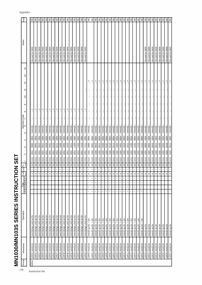
Appendix
178 Instruction Set
UD
F20
imm
16,D
n�
UD
F21
imm
16,D
n�
UD
F22
imm
16,D
n�
UD
F23
imm
16,D
n�
UD
F24
imm
16,D
n�
UD
F25
imm
16,D
n�
UD
F26
imm
16,D
n�
UD
F27
imm
16,D
n�
UD
F28
imm
16,D
n�
UD
F29
imm
16,D
n�
UD
F30
imm
16,D
n�
UD
F31
imm
16,D
n�
UD
F32
imm
16,D
n�
UD
F33
imm
16,D
n�
UD
F34
imm
16,D
n�
UD
F35
imm
16,D
n�
UD
F00
imm
32,D
n�
UD
F01
imm
32,D
n�
UD
F02
imm
32,D
n�
UD
F03
imm
32,D
n�
UD
F04
imm
32,D
n�
UD
F05
imm
32,D
n�
UD
F06
imm
32,D
n�
UD
F07
imm
32,D
n�
UD
F08
imm
32,D
n�
UD
F09
imm
32,D
n�
UD
F10
imm
32,D
n�
UD
F11
imm
32,D
n�
UD
F12
imm
32,D
n�
UD
F13
imm
32,D
n�
UD
F14
imm
32,D
n�
UD
F15
imm
32,D
n�
UD
F20
imm
32,D
n�
UD
F21
imm
32,D
n�
UD
F22
imm
32,D
n�
UD
F23
imm
32,D
n�
UD
F24
imm
32,D
n�
UD
F25
imm
32,D
n�
UD
F26
imm
32,D
n�
UD
F27
imm
32,D
n�
� �
imm
16(s
ign_
ext)
op
Dn�
imm
16(s
ign_
ext)
op
Dn�
imm
16(s
ign_
ext)
op
Dn�
imm
16(s
ign_
ext)
op
Dn�
imm
16(s
ign_
ext)
op
Dn�
imm
16(s
ign_
ext)
op
Dn�
imm
16(s
ign_
ext)
op
Dn�
imm
16(s
ign_
ext)
op
Dn�
imm
16(s
ign_
ext)
op
Dn�
imm
16(s
ign_
ext)
op
Dn�
imm
16(s
ign_
ext)
op
Dn�
imm
16(s
ign_
ext)
op
Dn�
imm
16(s
ign_
ext)
op
Dn�
imm
16(s
ign_
ext)
op
Dn�
imm
16(s
ign_
ext)
op
Dn�
imm
16(s
ign_
ext)
op
Dn�
imm
32 o
p D
n →
Dn�
imm
32 o
p D
n →
Dn�
imm
32 o
p D
n →
Dn�
imm
32 o
p D
n →
Dn�
imm
32 o
p D
n →
Dn�
imm
32 o
p D
n →
Dn�
imm
32 o
p D
n →
Dn�
imm
32 o
p D
n →
Dn�
imm
32 o
p D
n →
Dn�
imm
32 o
p D
n →
Dn�
imm
32 o
p D
n →
Dn�
imm
32 o
p D
n →
Dn�
imm
32 o
p D
n →
Dn�
imm
32 o
p D
n →
Dn�
imm
32 o
p D
n →
Dn�
imm
32 o
p D
n →
Dn�
imm
32 o
p D
n�
imm
32 o
p D
n�
imm
32 o
p D
n�
imm
32 o
p D
n�
imm
32 o
p D
n�
imm
32 o
p D
n�
imm
32 o
p D
n�
imm
32 o
p D
n�
�
-� -� -� -� -� -� -� -� -� -� -� -� -� -� -� -� *� *� *� *� *� *� *� *� *� *� *� *� *� *� *� *� -� -� -� -� -� -� -� -
-� -� -� -� -� -� -� -� -� -� -� -� -� -� -� -� *� *� *� *� *� *� *� *� *� *� *� *� *� *� *� *� -� -� -� -� -� -� -� -
-� -� -� -� -� -� -� -� -� -� -� -� -� -� -� -� *� *� *� *� *� *� *� *� *� *� *� *� *� *� *� *� -� -� -� -� -� -� -� -
-� -� -� -� -� -� -� -� -� -� -� -� -� -� -� -� *� *� *� *� *� *� *� *� *� *� *� *� *� *� *� *� -� -� -� -� -� -� -� -
4� 4� 4� 4� 4� 4� 4� 4� 4� 4� 4� 4� 4� 4� 4� 4� 6� 6� 6� 6� 6� 6� 6� 6� 6� 6� 6� 6� 6� 6� 6� 6� 6� 6� 6� 6� 6� 6� 6� 6
*� *� *� *� *� *� *� *� *� *� *� *� *� *� *� *� *� *� *� *� *� *� *� *� *� *� *� *� *� *� *� *� *� *� *� *� *� *� *� *� �
D2�
D2�
D2�
D2�
D2�
D2�
D2�
D2�
D2�
D2�
D2�
D2�
D2�
D2�
D2�
D2�
D4�
D4�
D4�
D4�
D4�
D4�
D4�
D4�
D4�
D4�
D4�
D4�
D4�
D4�
D4�
D4�
D4�
D4�
D4�
D4�
D4�
D4�
D4�
D4
1� � 1111
�
1111
�
1111
�
1111
�
1111
�
1111
�
1111
�
1111
�
1111
�
1111
�
1111
�
1111
�
1111
�
1111
�
1111
�
1111
�
1111
�
1111
�
1111
�
1111
�
1111
�
1111
�
1111
�
1111
�
1111
�
1111
�
1111
�
1111
�
1111
�
1111
�
1111
�
1111
�
1111
�
1111
�
1111
�
1111
�
1111
�
1111
�
1111
�
1111
2� � 1011
�
1011
�
1011
�
1011
�
1011
�
1011
�
1011
�
1011
�
1011
�
1011
�
1011
�
1011
�
1011
�
1011
�
1011
�
1011
�
1101
�
1101
�
1101
�
1101
�
1101
�
1101
�
1101
�
1101
�
1101
�
1101
�
1101
�
1101
�
1101
�
1101
�
1101
�
1101
�
1101
�
1101
�
1101
�
1101
�
1101
�
1101
�
1101
�
1101
3� � 0000
�
0001
�
0010
�
0011
�
0100
�
0101
�
0110
�
0111
�
1000
�
1001
�
1010
�
1011
�
1100
�
1101
�
1110
�
1111
�
0000
�
0001
�
0010
�
0011
�
0100
�
0101
�
0110
�
0111
�
1000
�
1001
�
1010
�
1011
�
1100
�
1101
�
1110
�
1111
�
0000
�
0001
�
0010
�
0011
�
0100
�
0101
�
0110
�
0111
4� � 10D
n�
10D
n�
10D
n�
10D
n�
10D
n�
10D
n�
10D
n�
10D
n�
10D
n�
10D
n�
10D
n�
10D
n�
10D
n�
10D
n�
10D
n�
10D
n�
00D
n�
00D
n�
00D
n�
00D
n�
00D
n�
00D
n�
00D
n�
00D
n�
00D
n�
00D
n�
00D
n�
00D
n�
00D
n�
00D
n�
00D
n�
00D
n�
10D
n�
10D
n�
10D
n�
10D
n�
10D
n�
10D
n�
10D
n�
10D
n
5� � <im
m16
�
<im
m16
�
<im
m16
�
<im
m16
�
<im
m16
�
<im
m16
�
<im
m16
�
<im
m16
�
<im
m16
�
<im
m16
�
<im
m16
�
<im
m16
�
<im
m16
�
<im
m16
�
<im
m16
�
<im
m16
�
<im
m32
�
<im
m32
�
<im
m32
�
<im
m32
�
<im
m32
�
<im
m32
�
<im
m32
�
<im
m32
�
<im
m32
�
<im
m32
�
<im
m32
�
<im
m32
�
<im
m32
�
<im
m32
�
<im
m32
�
<im
m32
�
<im
m32
�
<im
m32
�
<im
m32
�
<im
m32
�
<im
m32
�
<im
m32
�
<im
m32
�
<im
m32
6� � ....�
....�
....�
....�
....�
....�
....�
....�
....�
....�
....�
....�
....�
....�
....�
....�
....�
....�
....�
....�
....�
....�
....�
....�
....�
....�
....�
....�
....�
....�
....�
....�
....�
....�
....�
....�
....�
....�
....�
....�
�
Gro
up�
�
Mne
mon
icO
pera
tion
Mac
hine
Cod
eN
otes
Pag
eF
lag
Cod
e�
Siz
eC
ycle
For
�
-m
at
MN
1030
/MN
103S
SE
RIE
S IN
ST
RU
CT
ION
SE
T7� � ...
.�
....�
....�
....�
....�
....�
....�
....�
....�
....�
....�
....�
....�
....�
....�
....�
....�
....�
....�
....�
....�
....�
....�
....�
....�
....�
....�
....�
....�
....�
....�
....�
....�
....�
....�
....�
....�
....�
....�
....
8� � ....>
�
....>
�
....>
�
....>
�
....>
�
....>
�
....>
�
....>
�
....>
�
....>
�
....>
�
....>
�
....>
�
....>
�
....>
�
....>
�
....�
....�
....�
....�
....�
....�
....�
....�
....�
....�
....�
....�
....�
....�
....�
....�
....�
....�
....�
....�
....�
....�
....�
....
9� � � � � � � � � � � � � � � � � � ....�
....�
....�
....�
....�
....�
....�
....�
....�
....�
....�
....�
....�
....�
....�
....�
....�
....�
....�
....�
....�
....�
....�
....
10�
� � � � � � � � � � � � � � � � � ....�
....�
....�
....�
....�
....�
....�
....�
....�
....�
....�
....�
....�
....�
....�
....�
....�
....�
....�
....�
....�
....�
....�
....�
�
11�
� � � � � � � � � � � � � � � � ....�
....�
....�
....�
....�
....�
....�
....�
....�
....�
....�
....�
....�
....�
....�
...�
....�
....�
....�
....�
....�
....�
....�
.....�
�
12�
� � � � � � � � � � � � � � � � � ....>
�
....>
�
....>
�
....>
�
....>
�
....>
�
....>
�
....>
�
....>
�
....>
�
....>
�
....>
�
....>
�
....>
�
....>
�
....>
�
....>
�
....>
�
....>
�
....>
�
....>
�
....>
�
....>
�
....>
�
�
13�
� � � � � � � � � � � � � � � � � � � � � � � � � � �
14V
FC
FN
FZ
F
UD
Fnn
�99
�
99�
99�
99�
99�
99�
99�
99�
99�
99�
99�
99�
99�
99�
99�
99�
99�
99�
99�
99�
99�
99�
99�
99�
99�
99�
99�
99�
99�
99�
99�
99�
99�
99�
99�
99�
99�
99�
99�
99
Not
use
d fo
r AM
30�
Not
use
d fo
r AM
30�
Not
use
d fo
r AM
30�
Not
use
d fo
r AM
30�
Not
use
d fo
r AM
30�
Not
use
d fo
r AM
30�
Not
use
d fo
r AM
30�
Not
use
d fo
r AM
30�
Not
use
d fo
r AM
30�
Not
use
d fo
r AM
30�
Not
use
d fo
r AM
30�
Not
use
d fo
r AM
30�
Not
use
d fo
r AM
30�
Not
use
d fo
r AM
30�
Not
use
d fo
r AM
30�
Not
use
d fo
r AM
30�
� � � � � � � � � � � � � � � � Not
use
d fo
r AM
30�
Not
use
d fo
r AM
30�
Not
use
d fo
r AM
30�
Not
use
d fo
r AM
30�
Not
use
d fo
r AM
30�
Not
use
d fo
r AM
30�
Not
use
d fo
r AM
30�
Not
use
d fo
r AM
30�
��
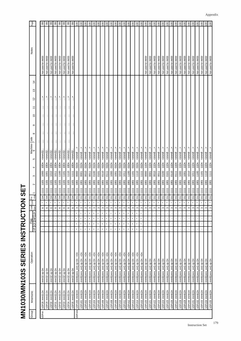
Appendix
179Instruction Set
UD
F28
imm
32,D
n�
UD
F29
imm
32,D
n�
UD
F30
imm
32,D
n�
UD
F31
imm
32,D
n�
UD
F32
imm
32,D
n�
UD
F33
imm
32,D
n�
UD
F34
imm
32,D
n�
UD
F35
imm
32,D
n�
UD
FU00
im
m8,
Dn�
UD
FU01
im
m8,
Dn�
UD
FU02
im
m8,
Dn�
UD
FU03
im
m8,
Dn�
UD
FU04
im
m8,
Dn�
UD
FU05
im
m8,
Dn�
UD
FU06
im
m8,
Dn�
UD
FU07
im
m8,
Dn�
UD
FU08
im
m8,
Dn�
UD
FU09
im
m8,
Dn�
UD
FU10
im
m8,
Dn�
UD
FU11
im
m8,
Dn�
UD
FU12
im
m8,
Dn�
UD
FU13
im
m8,
Dn�
UD
FU14
im
m8,
Dn�
UD
FU15
im
m8,
Dn�
UD
FU20
im
m8,
Dn�
UD
FU21
im
m8,
Dn�
UD
FU22
im
m8,
Dn�
UD
FU23
im
m8,
Dn�
UD
FU24
im
m8,
Dn�
UD
FU25
im
m8,
Dn�
UD
FU26
im
m8,
Dn�
UD
FU27
im
m8,
Dn�
UD
FU28
im
m8,
Dn�
UD
FU29
im
m8,
Dn�
UD
FU30
im
m8,
Dn�
UD
FU31
im
m8,
Dn�
UD
FU32
im
m8,
Dn�
UD
FU33
im
m8,
Dn�
UD
FU34
im
m8,
Dn�
UD
FU35
im
m8,
Dn�
�
imm
32 o
p D
n�
imm
32 o
p D
n�
imm
32 o
p D
n�
imm
32 o
p D
n�
imm
32 o
p D
n�
imm
32 o
p D
n�
imm
32 o
p D
n�
imm
32 o
p D
n�
imm
8(ze
ro_e
xt)
op D
n →
Dn�
imm
8(ze
ro_e
xt)
op D
n →
Dn�
imm
8(ze
ro_e
xt)
op D
n →
Dn�
imm
8(ze
ro_e
xt)
op D
n →
Dn�
imm
8(ze
ro_e
xt)
op D
n →
Dn�
imm
8(ze
ro_e
xt)
op D
n →
Dn�
imm
8(ze
ro_e
xt)
op D
n →
Dn�
imm
8(ze
ro_e
xt)
op D
n →
Dn�
imm
8(ze
ro_e
xt)
op D
n →
Dn�
imm
8(ze
ro_e
xt)
op D
n →
Dn�
imm
8(ze
ro_e
xt)
op D
n →
Dn�
imm
8(ze
ro_e
xt)
op D
n →
Dn�
imm
8(ze
ro_e
xt)
op D
n →
Dn�
imm
8(ze
ro_e
xt)
op D
n →
Dn�
imm
8(ze
ro_e
xt)
op D
n →
Dn�
imm
8(ze
ro_e
xt)
op D
n →
Dn�
imm
8(ze
ro_e
xt)
op D
n�
imm
8(ze
ro_e
xt)
op D
n�
imm
8(ze
ro_e
xt)
op D
n�
imm
8(ze
ro_e
xt)
op D
n�
imm
8(ze
ro_e
xt)
op D
n�
imm
8(ze
ro_e
xt)
op D
n�
imm
8(ze
ro_e
xt)
op D
n�
imm
8(ze
ro_e
xt)
op D
n�
imm
8(ze
ro_e
xt)
op D
n�
imm
8(ze
ro_e
xt)
op D
n�
imm
8(ze
ro_e
xt)
op D
n�
imm
8(ze
ro_e
xt)
op D
n�
imm
8(ze
ro_e
xt)
op D
n�
imm
8(ze
ro_e
xt)
op D
n�
imm
8(ze
ro_e
xt)
op D
n�
imm
8(ze
ro_e
xt)
op D
n
-� -� -� -� -� -� -� -� *� *� *� *� *� *� *� *� *� *� *� *� *� *� *� *� -� -� -� -� -� -� -� -� -� -� -� -� -� -� -� -� �
-� -� -� -� -� -� -� -� *� *� *� *� *� *� *� *� *� *� *� *� *� *� *� *� -� -� -� -� -� -� -� -� -� -� -� -� -� -� -� -� �
-� -� -� -� -� -� -� -� *� *� *� *� *� *� *� *� *� *� *� *� *� *� *� *� -� -� -� -� -� -� -� -� -� -� -� -� -� -� -� -� �
-� -� -� -� -� -� -� -� *� *� *� *� *� *� *� *� *� *� *� *� *� *� *� *� -� -� -� -� -� -� -� -� -� -� -� -� -� -� -� -� �
6� 6� 6� 6� 6� 6� 6� 6� 3� 3� 3� 3� 3� 3� 3� 3� 3� 3� 3� 3� 3� 3� 3� 3� 3� 3� 3� 3� 3� 3� 3� 3� 3� 3� 3� 3� 3� 3� 3� 3
*� *� *� *� *� *� *� *� *� *� *� *� *� *� *� *� *� *� *� *� *� *� *� *� *� *� *� *� *� *� *� *� *� *� *� *� *� *� *� *� �
D4�
D4�
D4�
D4�
D4�
D4�
D4�
D4�
D1�
D1�
D1�
D1�
D1�
D1�
D1�
D1�
D1�
D1�
D1�
D1�
D1�
D1�
D1�
D1�
D1�
D1�
D1�
D1�
D1�
D1�
D1�
D1�
D1�
D1�
D1�
D1�
D1�
D1�
D1�
D1� �
1� � 1111
�
1111
�
1111
�
1111
�
1111
�
1111
�
1111
�
1111
�
1111
�
1111
�
1111
�
1111
�
1111
�
1111
�
1111
�
1111
�
1111
�
1111
�
1111
�
1111
�
1111
�
1111
�
1111
�
1111
�
1111
�
1111
�
1111
�
1111
�
1111
�
1111
�
1111
�
1111
�
1111
�
1111
�
1111
�
1111
�
1111
�
1111
�
1111
�
1111
2� � 1101
�
1101
�
1101
�
1101
�
1101
�
1101
�
1101
�
1101
�
1001
�
1001
�
1001
�
1001
�
1001
�
1001
�
1001
�
1001
�
1001
�
1001
�
1001
�
1001
�
1001
�
1001
�
1001
�
1001
�
1001
�
1001
�
1001
�
1001
�
1001
�
1001
�
1001
�
1001
�
1001
�
1001
�
1001
�
1001
�
1001
�
1001
�
1001
�
1001
�
�
3� � 1000
�
1001
�
1010
�
1011
�
1100
�
1101
�
1110
�
1111
�
0000
�
0001
�
0010
�
0011
�
0100
�
0101
�
0110
�
0111
�
1000
�
1001
�
1010
�
1011
�
1100
�
1101
�
1110
�
1111
�
0000
�
0001
�
0010
�
0011
�
0100
�
0101
�
0110
�
0111
�
1000
�
1001
�
1010
�
1011
�
1100
�
1101
�
1110
�
1111
4� � 10D
n�
10D
n�
10D
n�
10D
n�
10D
n�
10D
n�
10D
n�
10D
n�
01D
n�
01D
n�
01D
n�
01D
n�
01D
n�
01D
n�
01D
n�
01D
n�
01D
n�
01D
n�
01D
n�
01D
n�
01D
n�
01D
n�
01D
n�
01D
n�
11D
n�
11D
n�
11D
n�
11D
n�
11D
n�
11D
n�
11D
n�
11D
n�
11D
n�
11D
n�
11D
n�
11D
n�
11D
n�
11D
n�
11D
n�
11D
n
5� � <im
m32
�
<im
m32
�
<im
m32
�
<im
m32
�
<im
m32
�
<im
m32
�
<im
m32
�
<im
m32
�
<im
m8�
<im
m8�
<im
m8�
<im
m8�
<im
m8�
<im
m8�
<im
m8�
<im
m8�
<im
m8�
<im
m8�
<im
m8�
<im
m8�
<im
m8�
<im
m8�
<im
m8�
<im
m8�
<im
m8�
<im
m8�
<im
m8�
<im
m8�
<im
m8�
<im
m8�
<im
m8�
<im
m8�
<im
m8�
<im
m8�
<im
m8�
<im
m8�
<im
m8�
<im
m8�
<im
m8�
<im
m8�
�
6� � ....�
....�
....�
....�
....�
....�
....�
....�
....>
�
....>
�
....>
�
....>
�
....>
�
....>
�
....>
�
....>
�
....>
�
....>
�
....>
�
....>
�
....>
�
....>
�
....>
�
....>
�
....>
�
....>
�
....>
�
....>
�
....>
�
....>
�
....>
�
....>
�
....>
�
....>
�
....>
�
....>
�
....>
�
....>
�
....>
�
....>
�
�
� �
Gro
up�
�
Mne
mon
icO
pera
tion
Mac
hine
Cod
eN
otes
Pag
eF
lag
Cod
e�
Siz
eC
ycle
For
�
-m
at
MN
1030
/MN
103S
SE
RIE
S IN
ST
RU
CT
ION
SE
T7� ...
.�
....�
....�
....�
....�
....�
....�
....�
� � � � � � � � � � � � � � � �
8� � ....�
....�
....�
....�
....�
....�
....�
....�
� � � � � � � � � � � � � � �
9� � ....�
....�
....�
....�
....�
....�
....�
....�
� � � � � � � � � � � � � � � � � � �
10�
� ....�
....�
....�
....�
....�
....�
....�
....�
� � � � � � � � � � � � � � � � � � �
11�
� ....�
....�
....�
....�
....�
....�
....�
....�
� � � � � � � � � � � � � � � � � � �
12�
� ....>
�
....>
�
....>
�
....>
�
....>
�
....>
�
....>
�
....>
�
� � � � � � � � � � � � � � � � � � �
1314
VF
CF
NF
ZF
UD
Fnn�
� � � � � � � UD
FUnn
�99
�
99�
99�
99�
99�
99�
99�
99�
100�
100�
100�
100�
100�
100�
100�
100�
100�
100�
100�
100�
100�
100�
100�
100�
100�
100�
100�
100�
100�
100�
100�
100�
100�
100�
100�
100�
100�
100�
100�
100
Not
use
d fo
r AM
30�
Not
use
d fo
r AM
30�
Not
use
d fo
r AM
30�
Not
use
d fo
r AM
30�
Not
use
d fo
r AM
30�
Not
use
d fo
r AM
30�
Not
use
d fo
r AM
30�
Not
use
d fo
r AM
30�
� � � � � � � � � � � � � � � � Not
use
d fo
r AM
30�
Not
use
d fo
r AM
30�
Not
use
d fo
r AM
30�
Not
use
d fo
r AM
30�
Not
use
d fo
r AM
30�
Not
use
d fo
r AM
30�
Not
use
d fo
r AM
30�
Not
use
d fo
r AM
30�
Not
use
d fo
r AM
30�
Not
use
d fo
r AM
30�
Not
use
d fo
r AM
30�
Not
use
d fo
r AM
30�
Not
use
d fo
r AM
30�
Not
use
d fo
r AM
30�
Not
use
d fo
r AM
30�
Not
use
d fo
r AM
30�
�
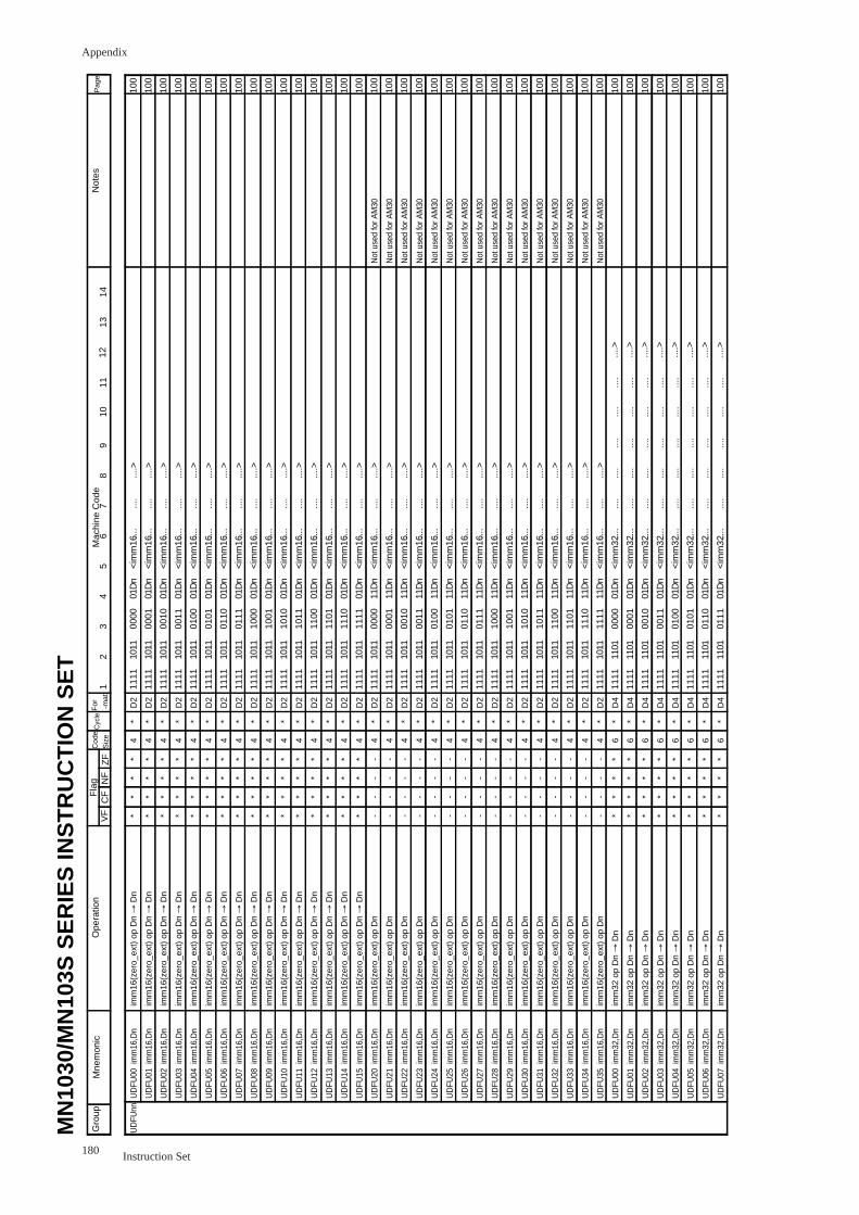
Appendix
180 Instruction Set
UD
FU00
im
m16
,Dn�
UD
FU01
im
m16
,Dn�
UD
FU02
im
m16
,Dn�
UD
FU03
im
m16
,Dn�
UD
FU04
im
m16
,Dn�
UD
FU05
im
m16
,Dn�
UD
FU06
im
m16
,Dn�
UD
FU07
im
m16
,Dn�
UD
FU08
im
m16
,Dn�
UD
FU09
im
m16
,Dn�
UD
FU10
im
m16
,Dn�
UD
FU11
im
m16
,Dn�
UD
FU12
im
m16
,Dn�
UD
FU13
im
m16
,Dn�
UD
FU14
im
m16
,Dn�
UD
FU15
im
m16
,Dn�
UD
FU20
im
m16
,Dn�
UD
FU21
im
m16
,Dn�
UD
FU22
im
m16
,Dn�
UD
FU23
im
m16
,Dn�
UD
FU24
im
m16
,Dn�
UD
FU25
im
m16
,Dn�
UD
FU26
im
m16
,Dn�
UD
FU27
im
m16
,Dn�
UD
FU28
im
m16
,Dn�
UD
FU29
im
m16
,Dn�
UD
FU30
im
m16
,Dn�
UD
FU31
im
m16
,Dn�
UD
FU32
im
m16
,Dn�
UD
FU33
im
m16
,Dn�
UD
FU34
im
m16
,Dn�
UD
FU35
im
m16
,Dn�
UD
FU00
im
m32
,Dn�
UD
FU01
im
m32
,Dn�
UD
FU02
im
m32
,Dn�
UD
FU03
im
m32
,Dn�
UD
FU04
im
m32
,Dn�
UD
FU05
im
m32
,Dn�
UD
FU06
im
m32
,Dn�
UD
FU07
im
m32
,Dn
imm
16(z
ero_
ext)
op
Dn →
Dn�
imm
16(z
ero_
ext)
op
Dn →
Dn�
imm
16(z
ero_
ext)
op
Dn →
Dn�
imm
16(z
ero_
ext)
op
Dn →
Dn�
imm
16(z
ero_
ext)
op
Dn →
Dn�
imm
16(z
ero_
ext)
op
Dn →
Dn�
imm
16(z
ero_
ext)
op
Dn →
Dn�
imm
16(z
ero_
ext)
op
Dn →
Dn�
imm
16(z
ero_
ext)
op
Dn →
Dn�
imm
16(z
ero_
ext)
op
Dn →
Dn�
imm
16(z
ero_
ext)
op
Dn →
Dn�
imm
16(z
ero_
ext)
op
Dn →
Dn�
imm
16(z
ero_
ext)
op
Dn →
Dn�
imm
16(z
ero_
ext)
op
Dn →
Dn�
imm
16(z
ero_
ext)
op
Dn →
Dn�
imm
16(z
ero_
ext)
op
Dn →
Dn�
imm
16(z
ero_
ext)
op
Dn�
imm
16(z
ero_
ext)
op
Dn�
imm
16(z
ero_
ext)
op
Dn�
imm
16(z
ero_
ext)
op
Dn�
imm
16(z
ero_
ext)
op
Dn�
imm
16(z
ero_
ext)
op
Dn�
imm
16(z
ero_
ext)
op
Dn�
imm
16(z
ero_
ext)
op
Dn�
imm
16(z
ero_
ext)
op
Dn�
imm
16(z
ero_
ext)
op
Dn�
imm
16(z
ero_
ext)
op
Dn�
imm
16(z
ero_
ext)
op
Dn�
imm
16(z
ero_
ext)
op
Dn�
imm
16(z
ero_
ext)
op
Dn�
imm
16(z
ero_
ext)
op
Dn�
imm
16(z
ero_
ext)
op
Dn�
imm
32 o
p D
n →
Dn�
imm
32 o
p D
n →
Dn�
imm
32 o
p D
n →
Dn�
imm
32 o
p D
n →
Dn�
imm
32 o
p D
n →
Dn�
imm
32 o
p D
n →
Dn�
imm
32 o
p D
n →
Dn�
imm
32 o
p D
n →
Dn
*� *� *� *� *� *� *� *� *� *� *� *� *� *� *� *� -� -� -� -� -� -� -� -� -� -� -� -� -� -� -� -� *� *� *� *� *� *� *� *
*� *� *� *� *� *� *� *� *� *� *� *� *� *� *� *� -� -� -� -� -� -� -� -� -� -� -� -� -� -� -� -� *� *� *� *� *� *� *� *
*� *� *� *� *� *� *� *� *� *� *� *� *� *� *� *� -� -� -� -� -� -� -� -� -� -� -� -� -� -� -� -� *� *� *� *� *� *� *� *
*� *� *� *� *� *� *� *� *� *� *� *� *� *� *� *� -� -� -� -� -� -� -� -� -� -� -� -� -� -� -� -� *� *� *� *� *� *� *� *
4� 4� 4� 4� 4� 4� 4� 4� 4� 4� 4� 4� 4� 4� 4� 4� 4� 4� 4� 4� 4� 4� 4� 4� 4� 4� 4� 4� 4� 4� 4� 4� 6� 6� 6� 6� 6� 6� 6� 6
*� *� *� *� *� *� *� *� *� *� *� *� *� *� *� *� *� *� *� *� *� *� *� *� *� *� *� *� *� *� *� *� *� *� *� *� *� *� *� *� �
D2�
D2�
D2�
D2�
D2�
D2�
D2�
D2�
D2�
D2�
D2�
D2�
D2�
D2�
D2�
D2�
D2�
D2�
D2�
D2�
D2�
D2�
D2�
D2�
D2�
D2�
D2�
D2�
D2�
D2�
D2�
D2�
D4�
D4�
D4�
D4�
D4�
D4�
D4�
D4
1� � 1111
�
1111
�
1111
�
1111
�
1111
�
1111
�
1111
�
1111
�
1111
�
1111
�
1111
�
1111
�
1111
�
1111
�
1111
�
1111
�
1111
�
1111
�
1111
�
1111
�
1111
�
1111
�
1111
�
1111
�
1111
�
1111
�
1111
�
1111
�
1111
�
1111
�
1111
�
1111
�
1111
�
1111
�
1111
�
1111
�
1111
�
1111
�
1111
�
1111
�
� �
2� � 1011
�
1011
�
1011
�
1011
�
1011
�
1011
�
1011
�
1011
�
1011
�
1011
�
1011
�
1011
�
1011
�
1011
�
1011
�
1011
�
1011
�
1011
�
1011
�
1011
�
1011
�
1011
�
1011
�
1011
�
1011
�
1011
�
1011
�
1011
�
1011
�
1011
�
1011
�
1011
�
1101
�
1101
�
1101
�
1101
�
1101
�
1101
�
1101
�
1101
3� � 0000
�
0001
�
0010
�
0011
�
0100
�
0101
�
0110
�
0111
�
1000
�
1001
�
1010
�
1011
�
1100
�
1101
�
1110
�
1111
�
0000
�
0001
�
0010
�
0011
�
0100
�
0101
�
0110
�
0111
�
1000
�
1001
�
1010
�
1011
�
1100
�
1101
�
1110
�
1111
�
0000
�
0001
�
0010
�
0011
�
0100
�
0101
�
0110
�
0111
4� � 01D
n�
01D
n�
01D
n�
01D
n�
01D
n�
01D
n�
01D
n�
01D
n�
01D
n�
01D
n�
01D
n�
01D
n�
01D
n�
01D
n�
01D
n�
01D
n�
11D
n�
11D
n�
11D
n�
11D
n�
11D
n�
11D
n�
11D
n�
11D
n�
11D
n�
11D
n�
11D
n�
11D
n�
11D
n�
11D
n�
11D
n�
11D
n�
01D
n�
01D
n�
01D
n�
01D
n�
01D
n�
01D
n�
01D
n�
01D
n�
�
5� � <im
m16
�
<im
m16
�
<im
m16
�
<im
m16
�
<im
m16
�
<im
m16
�
<im
m16
�
<im
m16
�
<im
m16
�
<im
m16
�
<im
m16
�
<im
m16
�
<im
m16
�
<im
m16
�
<im
m16
�
<im
m16
�
<im
m16
�
<im
m16
�
<im
m16
�
<im
m16
�
<im
m16
�
<im
m16
�
<im
m16
�
<im
m16
�
<im
m16
�
<im
m16
�
<im
m16
�
<im
m16
�
<im
m16
�
<im
m16
�
<im
m16
�
<im
m16
�
<im
m32
�
<im
m32
�
<im
m32
�
<im
m32
�
<im
m32
�
<im
m32
�
<im
m32
�
<im
m32
�
�
6� � ....�
....�
....�
....�
....�
....�
....�
....�
....�
....�
....�
....�
....�
....�
....�
....�
....�
....�
....�
....�
....�
....�
....�
....�
....�
....�
....�
....�
....�
....�
....�
....�
....�
....�
....�
....�
....�
....�
....�
....
� �
Gro
up�
�
Mne
mon
icO
pera
tion
Mac
hine
Cod
eN
otes
Pag
eF
lag
Cod
e�
Siz
eC
ycle
For
�
-m
at
MN
1030
/MN
103S
SE
RIE
S IN
ST
RU
CT
ION
SE
T7� � ...
.�
....�
....�
....�
....�
....�
....�
....�
....�
....�
....�
....�
....�
....�
....�
....�
....�
....�
....�
....�
....�
....�
....�
....�
....�
....�
....�
....�
....�
....�
....�
....�
....�
....�
....�
....�
....�
....�
....�
....
8� � ....>
�
....>
�
....>
�
....>
�
....>
�
....>
�
....>
�
....>
�
....>
�
....>
�
....>
�
....>
�
....>
�
....>
�
....>
�
....>
�
....>
�
....>
�
....>
�
....>
�
....>
�
....>
�
....>
�
....>
�
....>
�
....>
�
....>
�
....>
�
....>
�
....>
�
....>
�
....>
�
....�
....�
....�
....�
....�
....�
....�
....
9� � � � � � � � � � � � � � � � � � � � � � � � � � � � � � � � � � ....�
....�
....�
....�
....�
....�
....�
....
10�
� � � � � � � � � � � � � � � � � � � � � � � � � � � � � � � � � ....�
....�
....�
....�
....�
....�
....�
....
11�
� � � � � � � � � � � � � � � � � � � � � � � � � � � � � � � � � ....�
....�
....�
....�
....�
....�
....�
....
12�
� � � � � � � � � � � � � � � � � � � � � � � � � � � � � � � � � ....>
�
....>
�
....>
�
....>
�
....>
�
....>
�
....>
�
....>
1314
VF
CF
NF
ZF
UD
FUnn
�10
0�
100�
100�
100�
100�
100�
100�
100�
100�
100�
100�
100�
100�
100�
100�
100�
100�
100�
100�
100�
100�
100�
100�
100�
100�
100�
100�
100�
100�
100�
100�
100�
100�
100�
100�
100�
100�
100�
100�
100
� � � � � � � � � � � � � � � � Not
use
d fo
r AM
30�
Not
use
d fo
r AM
30�
Not
use
d fo
r AM
30�
Not
use
d fo
r AM
30�
Not
use
d fo
r AM
30�
Not
use
d fo
r AM
30�
Not
use
d fo
r AM
30�
Not
use
d fo
r AM
30�
Not
use
d fo
r AM
30�
Not
use
d fo
r AM
30�
Not
use
d fo
r AM
30�
Not
use
d fo
r AM
30�
Not
use
d fo
r AM
30�
Not
use
d fo
r AM
30�
Not
use
d fo
r AM
30�
Not
use
d fo
r AM
30�
�
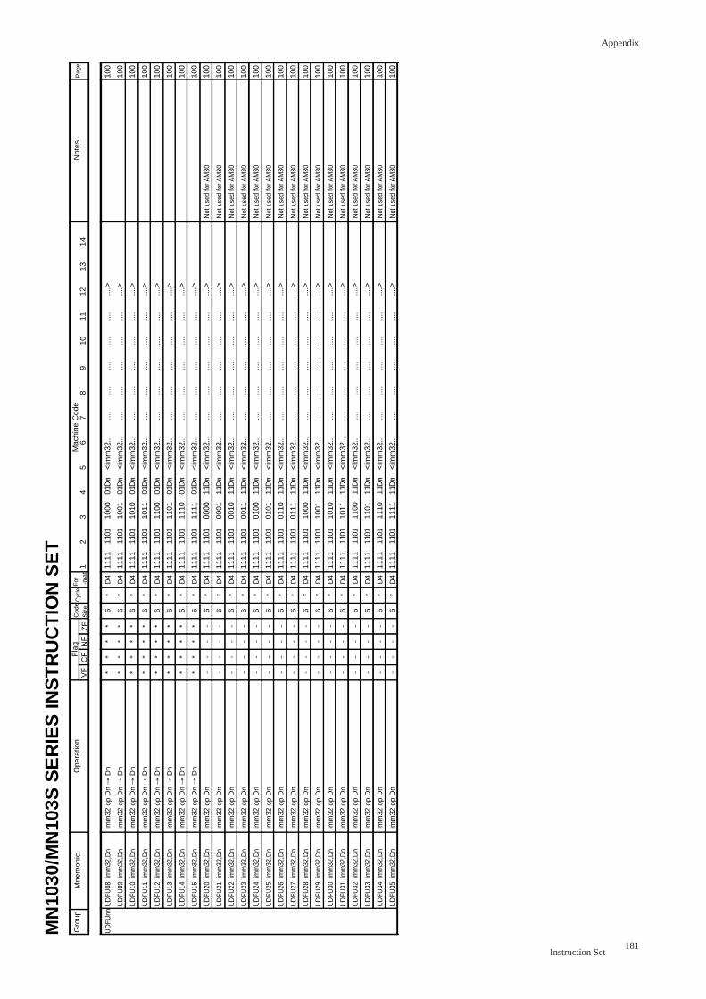
Appendix
181Instruction Set
UD
FU08
im
m32
,Dn�
UD
FU09
im
m32
,Dn�
UD
FU10
im
m32
,Dn�
UD
FU11
im
m32
,Dn�
UD
FU12
im
m32
,Dn�
UD
FU13
im
m32
,Dn�
UD
FU14
im
m32
,Dn�
UD
FU15
im
m32
,Dn�
UD
FU20
im
m32
,Dn�
UD
FU21
im
m32
,Dn�
UD
FU22
im
m32
,Dn�
UD
FU23
im
m32
,Dn�
UD
FU24
im
m32
,Dn�
UD
FU25
im
m32
,Dn�
UD
FU26
im
m32
,Dn�
UD
FU27
im
m32
,Dn�
UD
FU28
im
m32
,Dn�
UD
FU29
im
m32
,Dn�
UD
FU30
im
m32
,Dn�
UD
FU31
im
m32
,Dn�
UD
FU32
im
m32
,Dn�
UD
FU33
im
m32
,Dn�
UD
FU34
im
m32
,Dn�
UD
FU35
im
m32
,Dn
imm
32 o
p D
n →
Dn�
imm
32 o
p D
n →
Dn�
imm
32 o
p D
n →
Dn�
imm
32 o
p D
n →
Dn�
imm
32 o
p D
n →
Dn�
imm
32 o
p D
n →
Dn�
imm
32 o
p D
n →
Dn�
imm
32 o
p D
n →
Dn�
imm
32 o
p D
n�
imm
32 o
p D
n�
imm
32 o
p D
n�
imm
32 o
p D
n�
imm
32 o
p D
n�
imm
32 o
p D
n�
imm
32 o
p D
n�
imm
32 o
p D
n�
imm
32 o
p D
n�
imm
32 o
p D
n�
imm
32 o
p D
n�
imm
32 o
p D
n�
imm
32 o
p D
n�
imm
32 o
p D
n�
imm
32 o
p D
n�
imm
32 o
p D
n
*� *� *� *� *� *� *� *� -� -� -� -� -� -� -� -� -� -� -� -� -� -� -� -
*� *� *� *� *� *� *� *� -� -� -� -� -� -� -� -� -� -� -� -� -� -� -� -
*� *� *� *� *� *� *� *� -� -� -� -� -� -� -� -� -� -� -� -� -� -� -� -
*� *� *� *� *� *� *� *� -� -� -� -� -� -� -� -� -� -� -� -� -� -� -� -
6� 6� 6� 6� 6� 6� 6� 6� 6� 6� 6� 6� 6� 6� 6� 6� 6� 6� 6� 6� 6� 6� 6� 6
*� *� *� *� *� *� *� *� *� *� *� *� *� *� *� *� *� *� *� *� *� *� *� *� �
D4�
D4�
D4�
D4�
D4�
D4�
D4�
D4�
D4�
D4�
D4�
D4�
D4�
D4�
D4�
D4�
D4�
D4�
D4�
D4�
D4�
D4�
D4�
D4
1� � 1111
�
1111
�
1111
�
1111
�
1111
�
1111
�
1111
�
1111
�
1111
�
1111
�
1111
�
1111
�
1111
�
1111
�
1111
�
1111
�
1111
�
1111
�
1111
�
1111
�
1111
�
1111
�
1111
�
1111
�
� � �
2� � 1101
�
1101
�
1101
�
1101
�
1101
�
1101
�
1101
�
1101
�
1101
�
1101
�
1101
�
1101
�
1101
�
1101
�
1101
�
1101
�
1101
�
1101
�
1101
�
1101
�
1101
�
1101
�
1101
�
1101
�
� �
3� � 1000
�
1001
�
1010
�
1011
�
1100
�
1101
�
1110
�
1111
�
0000
�
0001
�
0010
�
0011
�
0100
�
0101
�
0110
�
0111
�
1000
�
1001
�
1010
�
1011
�
1100
�
1101
�
1110
�
1111
4� � 01D
n�
01D
n�
01D
n�
01D
n�
01D
n�
01D
n�
01D
n�
01D
n�
11D
n�
11D
n�
11D
n�
11D
n�
11D
n�
11D
n�
11D
n�
11D
n�
11D
n�
11D
n�
11D
n�
11D
n�
11D
n�
11D
n�
11D
n�
11D
n�
� �
5� � <im
m32
�
<im
m32
�
<im
m32
�
<im
m32
�
<im
m32
�
<im
m32
�
<im
m32
�
<im
m32
�
<im
m32
�
<im
m32
�
<im
m32
�
<im
m32
�
<im
m32
�
<im
m32
�
<im
m32
�
<im
m32
�
<im
m32
�
<im
m32
�
<im
m32
�
<im
m32
�
<im
m32
�
<im
m32
�
<im
m32
�
<im
m32
�
�
6� � ....�
....�
....�
....�
....�
....�
....�
....�
....�
....�
....�
....�
....�
....�
....�
....�
....�
....�
....�
....�
....�
....�
....�
....�
�
� �
Gro
up�
�
Mne
mon
icO
pera
tion
Mac
hine
Cod
eN
otes
Pag
eF
lag
Cod
e�
Siz
eC
ycle
For
�
-m
at
MN
1030
/MN
103S
SE
RIE
S IN
ST
RU
CT
ION
SE
T7� � ...
.�
....�
....�
....�
....�
....�
....�
....�
....�
....�
....�
....�
....�
....�
....�
....�
....�
....�
....�
....�
....�
....�
....�
....�
�
8� � ....�
....�
....�
....�
....�
....�
....�
....�
....�
....�
....�
....�
....�
....�
....�
....�
....�
....�
....�
....�
....�
....�
....�
....�
�
9� � ....�
....�
....�
....�
....�
....�
....�
....�
....�
....�
....�
....�
....�
....�
....�
....�
....�
....�
....�
....�
....�
....�
....�
....�
�
10�
� ....�
....�
....�
....�
....�
....�
....�
....�
....�
....�
....�
....�
....�
....�
....�
....�
....�
....�
....�
....�
....�
....�
....�
....�
�
11�
� ....�
....�
....�
....�
....�
....�
....�
....�
....�
....�
....�
....�
....�
....�
....�
....�
....�
....�
....�
....�
....�
....�
....�
....�
�
12�
� ....>
�
....>
�
....>
�
....>
�
....>
�
....>
�
....>
�
....>
�
....>
�
....>
�
....>
�
....>
�
....>
�
....>
�
....>
�
....>
�
....>
�
....>
�
....>
�
....>
�
....>
�
....>
�
....>
�
....>
�
�
1314
VF
CF
NF
ZF
UD
FUnn
�
�
100�
100�
100�
100�
100�
100�
100�
100�
100�
100�
100�
100�
100�
100�
100�
100�
100�
100�
100�
100�
100�
100�
100�
100
� � � � � � � � Not
use
d fo
r AM
30�
Not
use
d fo
r AM
30�
Not
use
d fo
r AM
30�
Not
use
d fo
r AM
30�
Not
use
d fo
r AM
30�
Not
use
d fo
r AM
30�
Not
use
d fo
r AM
30�
Not
use
d fo
r AM
30�
Not
use
d fo
r AM
30�
Not
use
d fo
r AM
30�
Not
use
d fo
r AM
30�
Not
use
d fo
r AM
30�
Not
use
d fo
r AM
30�
Not
use
d fo
r AM
30�
Not
use
d fo
r AM
30�
Not
use
d fo
r AM
30�
�
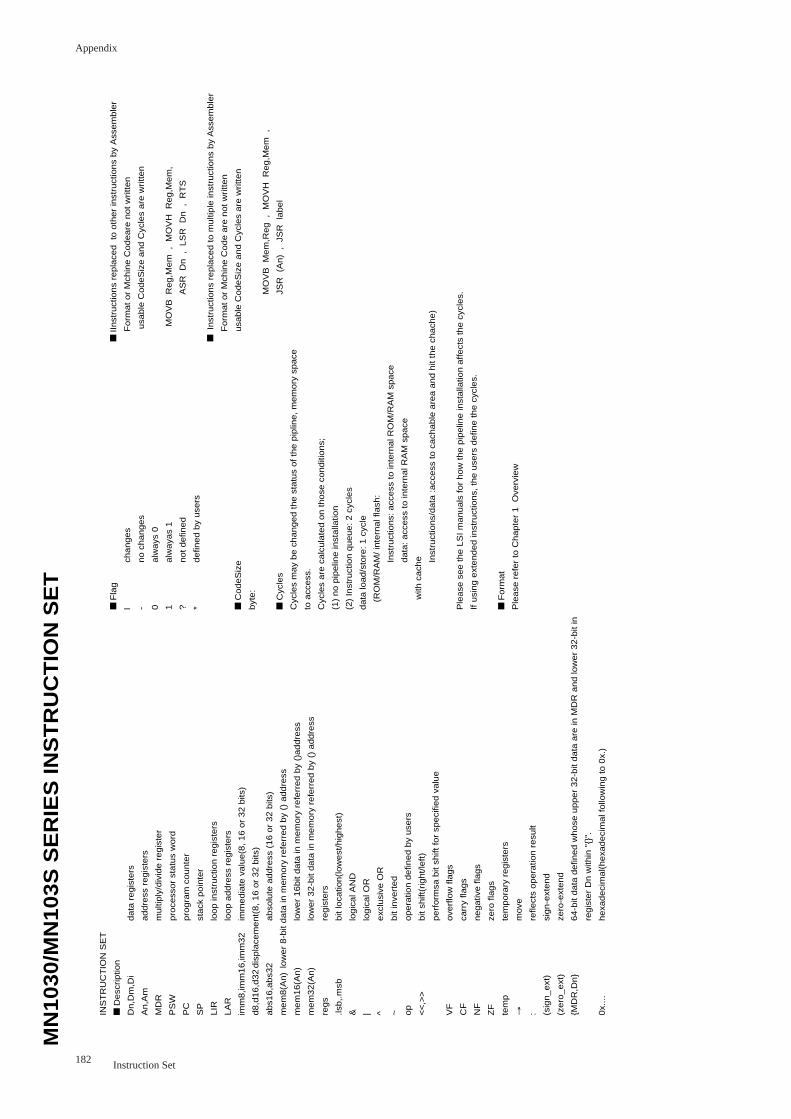
Appendix
182 Instruction Set
MN
1030/M
N103S
SE
RIE
S IN
ST
RU
CT
ION
SE
T
INS
TR
UC
TIO
N S
ET
�
■ D
esc
rip
tion
�
Dn
,Dm
,Di�
�d
ata
re
gis
ters
�
An
,Am
��
ad
dre
ss r
eg
iste
rs�
MD
R�
�m
ulti
ply
/div
ide
re
gis
ter�
PS
W�
�p
roce
sso
r st
atu
s w
ord
�
PC
��
pro
gra
m c
ou
nte
r�
SP
��
sta
ck p
oin
ter�
LIR
��
loo
p in
stru
ctio
n r
eg
iste
rs�
LA
R�
�lo
op
ad
dre
ss r
eg
iste
rs�
imm
8,im
m1
6,im
m3
2�
imm
ed
iate
va
lue
(8,
16
or
32
bits
)�
d8
,d1
6,d
32
�dis
pla
cem
en
t(8
, 1
6 o
r 3
2 b
its)�
ab
s16
,ab
s32
�a
bso
lute
ad
dre
ss (
16
or
32
bits
)�
me
m8
(An
)�lo
we
r 8
-bit
da
ta in
me
mo
ry r
efe
rre
d b
y ()
ad
dre
ss�
me
m1
6(A
n)�
low
er
16
bit
da
ta in
me
mo
ry r
efe
rre
d b
y ()
ad
dre
ss�
me
m3
2(A
n)�
low
er
32
-bit
da
ta in
me
mo
ry r
efe
rre
d b
y ()
ad
dre
ss�
reg
s��
reg
iste
rs�
.lsb
,.m
sb�
�b
it lo
catio
n(lo
we
st/h
igh
est
)�
&�
�lo
gic
al A
ND
�
|��
log
ica
l OR
�
^��
exc
lusi
ve O
R�
~�
�b
it in
vert
ed
�
op
��
op
era
tion
de
fine
d b
y u
sers
�
<<
,>>
��
bit
shift
(rig
ht/
left
)�
��
pe
rfo
rmsa
bit
shift
fo
r sp
eci
fied
va
lue
�
VF
��
ove
rflo
w f
lag
s�
CF
��
carr
y fla
gs�
NF
��
ne
ga
tive
fla
gs�
ZF
��
zero
fla
gs�
tem
p�
�te
mp
ora
ry r
eg
iste
rs�
→�
�m
ove
�
:��
refle
cts
op
era
tion
re
sult�
(sig
n_
ext
)��
sig
n-e
xte
nd
�
(ze
ro_
ext
)��
zero
-ext
en
d�
{MD
R,D
n}�
�6
4-b
it d
ata
de
fine
d w
ho
se u
pp
er
32
-bit
da
ta a
re in
MD
R a
nd
low
er
32
-bit
in �
��
reg
iste
r D
n w
ithin
"{}
".�
0x.
...�
�h
exa
de
cim
al(h
exa
de
cim
al f
ollo
win
g t
o 0
x.)
�
■ F
lag
�
l�ch
an
ge
s�
-�n
o c
ha
ng
es�
0�
alw
ays
0�
1�
alw
aya
s 1
�
?�
no
t d
efin
ed
�
*�d
efin
ed
by
use
rs�
� � ■ C
od
eS
ize
�
byt
e:�
� ■ C
ycle
s�
Cyc
les
ma
y b
e c
ha
ng
ed
th
e s
tatu
s o
f th
e p
iplin
e,
me
mo
ry s
pa
ce�
to a
cce
ss.�
Cyc
les
are
ca
lcu
late
d o
n t
ho
se c
on
diti
on
s;�
(1)
no
pip
elin
e in
sta
llatio
n�
(2)
Inst
ruct
ion
qu
eu
e:
2 c
ycle
s �
da
ta lo
ad
/sto
re:
1 c
ycle
�
(
RO
M/R
AM
/ in
tern
al f
lash
:�
�In
stru
ctio
ns:
acc
ess
to
inte
rna
l RO
M/R
AM
sp
ace
�
�d
ata
: a
cce
ss t
o in
tern
al R
AM
sp
ace
�
with
ca
che
�
�In
stru
ctio
ns/
da
ta :
acc
ess
to
ca
cha
ble
are
a a
nd
hit
the
ch
ach
e)�
� Ple
ase
se
e t
he
LS
I m
an
ua
ls f
or
ho
w t
he
pip
elin
e in
sta
llatio
n a
ffe
cts
the
cyc
les.
�
If u
sin
g e
xte
nd
ed
inst
ruct
ion
s, t
he
use
rs d
efin
e t
he
cyc
les.
�
� ■ F
orm
at�
Ple
ase
re
fer
to C
ha
pte
r 1
O
verv
iew
�
� �
■ I
Inst
ruct
ion
s re
pla
ced
to
oth
er
inst
ruct
ion
s b
y A
sse
mb
ler�
Fo
rma
t o
r M
chin
e C
od
ea
re n
ot
writt
en
�
usa
ble
Co
de
Siz
e a
nd
Cyc
les
are
writt
en
�
�
M
OV
B
Re
g,M
em
,
MO
VH
R
eg
,Me
m,�
�A
SR
D
n
, L
SR
D
n
, R
TS
�
� ■
Inst
ruct
ion
s re
pla
ced
to
mu
ltip
le in
stru
ctio
ns
by
Ass
em
ble
r
Fo
rma
t o
r M
chin
e C
od
e a
re n
ot
writt
en
�
usa
ble
Co
de
Siz
e a
nd
Cyc
les
are
writt
en
�
� �M
OV
B
Me
m,R
eg
,
MO
VH
R
eg
,Me
m
,�
�JS
R
(An
) ,
JS
R
lab
el
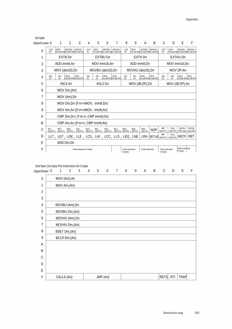
Appendix
183Instruction map
0 1 2 3 4 5 6 7 8 9 A B C D E F
0
1
2
3
4
5
6
7
8
9
A
B
C
D
E
F
0 1 2 3 4 5 6 7 8 9 A B C D E F
0
1
2
3
4
5
6
7
8
9
A
B
C
D
E
F
INC4 An
ADD imm8,An ADD imm8,Dn
CMP Am,An (If m=n, CMP imm8,An)
MOV Dm,(An)
MOV (Am),Dn
MOV (abs16),Dn
EXTH Dn
NOP
1st byte
Upper/Lower
2nd byte (1st byte:F0) Instruction for 2-byte
Upper/lower
MOV Am,(An)
MOV (Am),An
MOVBU (abs16),Dn
BSET Dm,(An)
BCLR Dm,(An)
ADD Dm,Dn
EXTB Dn
LHILGE LCCLLE LLSLLT LCS LEQ LNELGT
BHI(d8,PC)
BGE(d8,PC)
BCC(d8,PC)
BLE(d8,PC)
BLS(d8,PC)
BLT(d8,PC)
BCS(d8,PC)
BEQ(d8,PC)
BNE(d8,PC)
BGT(d8,PC)
BRA(d8,PC)
JMP(d16,PC)
Code extension (2-byte)
MOVBU (Am),Dn
MOV SP,An
MOV (d8,SP),Dn MOV (d8,SP),An
MOV Am,An (If m=nMOV, imm8,An)
CMP Dm,Dn ( If m=n, CMP imm8,Dn)
Code extension(3-byte)
Code extension
JMP (An)CALLS (An)
SETLB
MOV Dm,Dn (If m=nMOV, imm8,Dn)
ASL2 Dn
LRA
Code extension( 6-byte)
RET
CALL(d16,PC)
CALL(d32,PC)
MOVMregs,(SP)
MOVM(SP),regs
RETFJMP
(d32,PC)
MOV imm16,DnMOV imm16,An
MOVHU (abs16),Dn
EXTHU DnEXTBU Dn
Code extension(7-byte)
MOVHU Dm,(An)
MOVHU (Am),Dn
MOVBU Dm,(An)
RTI TRAPRETS
CLRD0
MOVD0,(abs16)
MOVBUD0,(abs16)
MOVHUD0,(abs16)
CLRD1
MOVD1,(abs16)
MOVBUD1,(abs16)
MOVHUD1,(abs16)
CLRD2
MOVD2,(abs16)
MOVBUD2,(abs16)
MOVHUD2,(abs16)
CLRD3
MOVD3,(abs16)
MOVBUD3,(abs16)
MOVHUD3,(abs16)
INCD0
INCA0
MOVD0,(d8,SP)
MOVA0,(d8,SP)
INCD1
INCA1
MOVD1,(d8,SP)
MOVA1,(d8,SP)
INCD2
INCA2
MOVD2,(d8,SP)
MOVA2,(d8,SP)
INCD3
INCA3
MOVD3,(d8,SP)
MOVA3,(d8,SP)
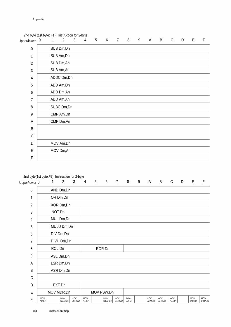
Appendix
Instruction map184
0 1 2 3 4 5 6 7 8 9 A B C D E F
0
1
2
3
4
5
6
7
8
9
A
B
C
D
E
F
0 1 2 3 4 5 6 7 8 9 A B C D E F
0
1
2
3
4
5
6
7
8
9
A
B
C
D
E
F
SUB Dm,Dn
SUB Am,Dn
CMP Dm,An
MOV Am,Dn
ADD Am,Dn
SUB Dm,An
MOV MDR,Dn MOV PSW,Dn
AND Dm,Dn
OR Dm,Dn
XOR Dm,Dn
ROL Dn ROR Dn
MUL Dm,Dn
MULU Dm,Dn
DIV Dm,Dn
ADDC Dm,Dn
SUBC Dm,Dn
NOT Dn
ADD Dm,An
SUB Am,An
CMP Am,Dn
ADD Am,An
MOV Dm,An
ASR Dm,Dn
LSR Dm,Dn
MOVD0,MDR
MOVD0,PSW
2nd byte (1st byte: F1)) Instruction for 2-byte
Upper/lower
2nd byte(1st byte:F2) Instruction for 2-byte
Upper/lower
EXT Dn
DIVU Dm,Dn
ASL Dm,Dn
MOVA0,SP
MOVD1,MDR
MOVD1,PSW
MOVA1,SP
MOVD2,MDR
MOVD2,PSW
MOVA2,SP
MOVD3,MDR
MOVD3,PSW
MOVA3,SP
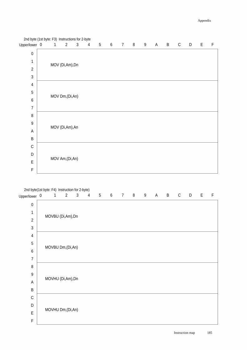
Appendix
185Instruction map
2nd byte(1st byte: F4) Instruction for 2-byte)
Upper/lower
MOVBU (Di,Am),Dn
MOVHU (Di,Am),Dn
MOV Dm,(Di,An)
MOV Am,(Di,An)
MOV (Di,Am),Dn
MOV (Di,Am),An
2nd byte (1st byte: F3) Instructions for 2-byte
Upper/lower
MOVBU Dm,(Di,An)
MOVHU Dm,(Di,An)
0
1
2
3
4
5
6
7
8
9
A
B
C
D
E
F
0
1
2
3
4
5
6
7
8
9
A
B
C
D
E
F
0 1 2 3 4 5 6 7 8 9 A B C D E F
0 1 2 3 4 5 6 7 8 9 A B C D E F
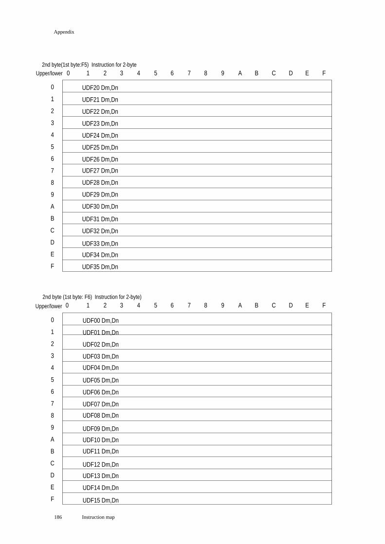
Appendix
Instruction map186
2nd byte(1st byte:F5) Instruction for 2-byteUpper/lower
2nd byte (1st byte: F6) Instruction for 2-byte)
Upper/lower
UDF00 Dm,Dn
UDF20 Dm,Dn
UDF21 Dm,Dn
UDF01 Dm,Dn
UDF02 Dm,Dn
UDF03 Dm,Dn
UDF04 Dm,Dn
UDF05 Dm,Dn
UDF06 Dm,Dn
UDF07 Dm,Dn
UDF08 Dm,Dn
UDF09 Dm,Dn
UDF10 Dm,Dn
UDF11 Dm,Dn
UDF12 Dm,Dn
UDF13 Dm,Dn
UDF14 Dm,Dn
UDF15 Dm,Dn
0
1
2
3
4
5
6
7
8
9
A
B
C
D
E
F
0
1
2
3
4
5
6
7
8
9
A
B
C
D
E
F
0 1 2 3 4 5 6 7 8 9 A B C D E F
0 1 2 3 4 5 6 7 8 9 A B C D E F
UDF22 Dm,Dn
UDF23 Dm,Dn
UDF24 Dm,Dn
UDF25 Dm,Dn
UDF26 Dm,Dn
UDF27 Dm,Dn
UDF28 Dm,Dn
UDF29 Dm,Dn
UDF30 Dm,Dn
UDF31 Dm,Dn
UDF32 Dm,Dn
UDF33 Dm,Dn
UDF34 Dm,Dn
UDF35 Dm,Dn
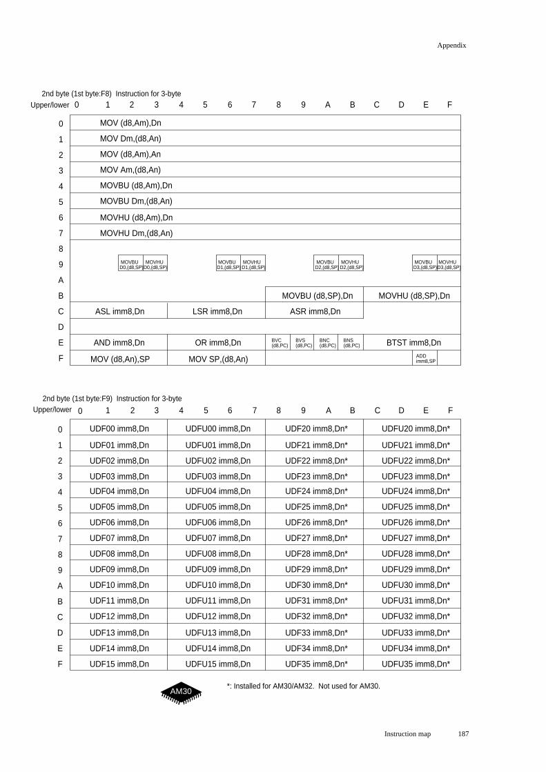
Appendix
187Instruction map
0 1 2 3 4 5 6 7 8 9 A B C D E F
0
1
2
3
4
5
6
7
8
9
A
B
C
D
E
F
0 1 2 3 4 5 6 7 8 9 A B C D E F
0
1
2
3
4
5
6
7
8
9
A
B
C
D
E
F
2nd byte (1st byte:F8) Instruction for 3-byteUpper/lower
2nd byte (1st byte:F9) Instruction for 3-byteUpper/lower
MOV Am,(d8,An)
MOVBU (d8,Am),Dn
MOVHU (d8,Am),Dn
BVC(d8,PC)
BVS(d8,PC)
BNC(d8,PC)
BNS(d8,PC)
MOV (d8,Am),An
MOV (d8,Am),Dn
MOV Dm,(d8,An)
UDF00 imm8,Dn
UDF01 imm8,Dn
UDF02 imm8,Dn
UDF03 imm8,Dn
UDF04 imm8,Dn
UDF05 imm8,Dn
UDF06 imm8,Dn
UDF07 imm8,Dn
UDF08 imm8,Dn
UDF09 imm8,Dn
UDF10 imm8,Dn
UDF11 imm8,Dn
UDF12 imm8,Dn
UDF13 imm8,Dn
UDF14 imm8,Dn
UDF15 imm8,Dn
MOVBU Dm,(d8,An)
MOVHU Dm,(d8,An)
AND imm8,Dn OR imm8,Dn BTST imm8,DnADDimm8,SP
ASL imm8,Dn LSR imm8,Dn ASR imm8,Dn
MOVBU (d8,SP),Dn MOVHU (d8,SP),Dn
MOVBUD0,(d8,SP)
MOVHUD0,(d8,SP)
MOVBUD1,(d8,SP)
MOVHUD1,(d8,SP)
MOVBUD2,(d8,SP)
MOVHUD2,(d8,SP)
MOVBUD3,(d8,SP)
MOVHUD3,(d8,SP)
UDFU00 imm8,Dn
UDFU01 imm8,Dn
UDFU02 imm8,Dn
UDFU03 imm8,Dn
UDFU04 imm8,Dn
UDFU05 imm8,Dn
UDFU06 imm8,Dn
UDFU07 imm8,Dn
UDFU08 imm8,Dn
UDFU09 imm8,Dn
UDFU10 imm8,Dn
UDFU11 imm8,Dn
UDFU12 imm8,Dn
UDFU13 imm8,Dn
UDFU14 imm8,Dn
UDFU15 imm8,Dn
MOV (d8,An),SP MOV SP,(d8,An)
UDF20 imm8,Dn*
UDF21 imm8,Dn*
UDF22 imm8,Dn*
UDF23 imm8,Dn*
UDF24 imm8,Dn*
UDF25 imm8,Dn*
UDF26 imm8,Dn*
UDF27 imm8,Dn*
UDF28 imm8,Dn*
UDF29 imm8,Dn*
UDF30 imm8,Dn*
UDF31 imm8,Dn*
UDF32 imm8,Dn*
UDF33 imm8,Dn*
UDF34 imm8,Dn*
UDF35 imm8,Dn*
UDFU20 imm8,Dn*
UDFU21 imm8,Dn*
UDFU22 imm8,Dn*
UDFU23 imm8,Dn*
UDFU24 imm8,Dn*
UDFU25 imm8,Dn*
UDFU26 imm8,Dn*
UDFU27 imm8,Dn*
UDFU28 imm8,Dn*
UDFU29 imm8,Dn*
UDFU30 imm8,Dn*
UDFU31 imm8,Dn*
UDFU32 imm8,Dn*
UDFU33 imm8,Dn*
UDFU34 imm8,Dn*
UDFU35 imm8,Dn*
*: Installed for AM30/AM32. Not used for AM30.AM30
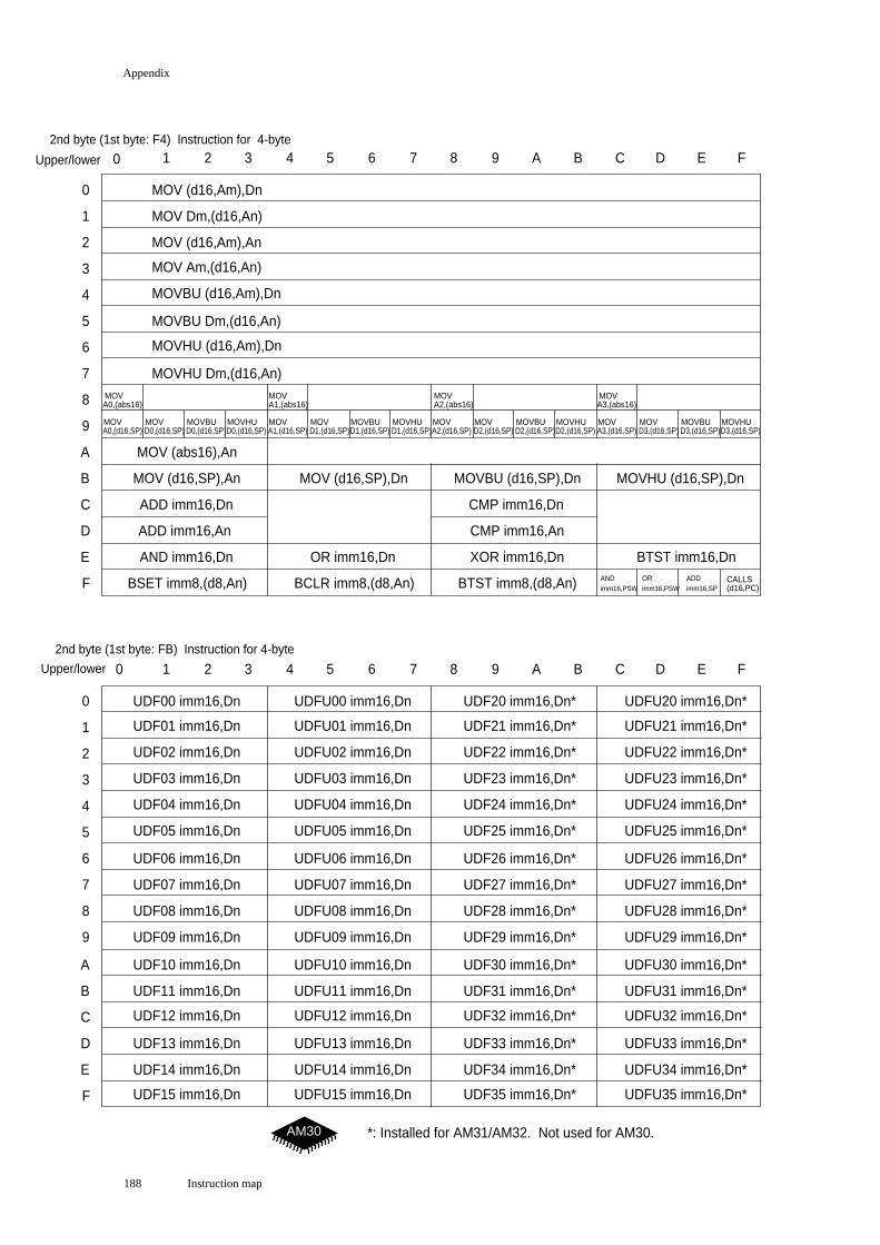
Appendix
Instruction map188
0 1 2 3 4 5 6 7 8 9 A B C D E F
0
1
2
3
4
5
6
7
8
9
A
B
C
D
E
F
0 1 2 3 4 5 6 7 8 9 A B C D E F
0
1
2
3
4
5
6
7
8
9
A
B
C
D
E
F
2nd byte (1st byte: FB) Instruction for 4-byte
Upper/lower
2nd byte (1st byte: F4) Instruction for 4-byte
Upper/lower
UDF00 imm16,Dn
MOV (d16,Am),Dn
MOV Dm,(d16,An)
MOV (d16,Am),An
MOV Am,(d16,An)
ANDimm16,PSW
ORimm16,PSW
UDF01 imm16,Dn
UDF02 imm16,Dn
UDF03 imm16,Dn
UDF04 imm16,Dn
UDF05 imm16,Dn
UDF06 imm16,Dn
UDF07 imm16,Dn
UDF08 imm16,Dn
UDF09 imm16,Dn
UDF10 imm16,Dn
UDF11 imm16,Dn
UDF12 imm16,Dn
UDF13 imm16,Dn
UDF14 imm16,Dn
UDF15 imm16,Dn
MOVBU (d16,Am),Dn
MOVHU (d16,Am),Dn
MOVBU Dm,(d16,An)
MOVHU Dm,(d16,An)
BSET imm8,(d8,An) BCLR imm8,(d8,An) CALLS(d16,PC)
ADDimm16,SPBTST imm8,(d8,An)
ADD imm16,An
ADD imm16,Dn CMP imm16,Dn
AND imm16,Dn OR imm16,Dn XOR imm16,Dn BTST imm16,Dn
MOVA0,(abs16)
MOV (abs16),An
MOV (d16,SP),Dn
MOVD0,(d16,SP)
MOV (d16,SP),An
MOVA0,(d16,SP)
MOVBU (d16,SP),Dn MOVHU (d16,SP),Dn
MOVBUD0,(d16,SP)
MOVHUD0,(d16,SP)
MOVA1,(abs16)
MOVD1,(d16,SP)
MOVA1,(d16,SP)
MOVBUD1,(d16,SP)
MOVHUD1,(d16,SP)
MOVA2,(abs16)
MOVD2,(d16,SP)
MOVA2,(d16,SP)
MOVBUD2,(d16,SP)
MOVHUD2,(d16,SP)
MOVA3,(abs16)
MOVD3,(d16,SP)
MOVA3,(d16,SP)
MOVBUD3,(d16,SP)
MOVHUD3,(d16,SP)
CMP imm16,An
UDFU00 imm16,Dn
UDFU01 imm16,Dn
UDFU02 imm16,Dn
UDFU03 imm16,Dn
UDFU04 imm16,Dn
UDFU05 imm16,Dn
UDFU06 imm16,Dn
UDFU07 imm16,Dn
UDFU08 imm16,Dn
UDFU09 imm16,Dn
UDFU10 imm16,Dn
UDFU11 imm16,Dn
UDFU12 imm16,Dn
UDFU13 imm16,Dn
UDFU14 imm16,Dn
UDFU15 imm16,Dn
UDF20 imm16,Dn*
UDF21 imm16,Dn*
UDF22 imm16,Dn*
UDF23 imm16,Dn*
UDF24 imm16,Dn*
UDF25 imm16,Dn*
UDF26 imm16,Dn*
UDF27 imm16,Dn*
UDF28 imm16,Dn*
UDF29 imm16,Dn*
UDF30 imm16,Dn*
UDF31 imm16,Dn*
UDF32 imm16,Dn*
UDF33 imm16,Dn*
UDF34 imm16,Dn*
UDF35 imm16,Dn*
UDFU20 imm16,Dn*
UDFU21 imm16,Dn*
UDFU22 imm16,Dn*
UDFU23 imm16,Dn*
UDFU24 imm16,Dn*
UDFU25 imm16,Dn*
UDFU26 imm16,Dn*
UDFU27 imm16,Dn*
UDFU28 imm16,Dn*
UDFU29 imm16,Dn*
UDFU30 imm16,Dn*
UDFU31 imm16,Dn*
UDFU32 imm16,Dn*
UDFU33 imm16,Dn*
UDFU34 imm16,Dn*
UDFU35 imm16,Dn*
*: Installed for AM31/AM32. Not used for AM30.AM30
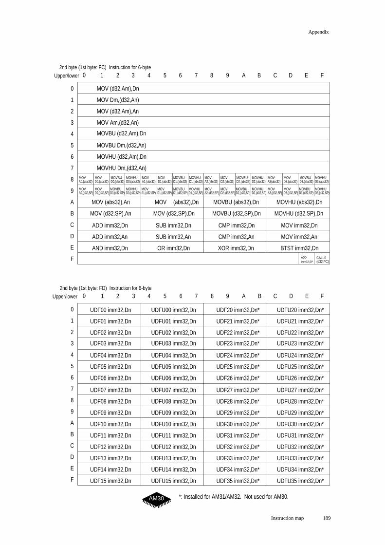
Appendix
189Instruction map
2nd byte (1st byte: FC) Instruction for 6-byte
Upper/lower
2nd byte (1st byte: FD) Instruction for 6-byte
Upper/lower
ADD imm32,An
ADD imm32,Dn
SUB imm32,An
SUB imm32,Dn
CMP imm32,An
CMP imm32,Dn
AND imm32,Dn OR imm32,Dn XOR imm32,Dn BTST imm32,Dn
MOVD0,(abs32)
MOV (abs32),Dn MOVHU (abs32),DnMOVBU (abs32),Dn
MOVA0,(abs32)
MOV (abs32),An
MOV (d32,Am),Dn
MOV Dm,(d32,An)
MOV (d32,Am),An
MOV Am,(d32,An)
MOV (d32,SP),Dn
MOVD0,(d32,SP)
MOV (d32,SP),An
MOVA0,(d32,SP)
UDF00 imm32,Dn
UDF01 imm32,Dn
UDF02 imm32,Dn
UDF03 imm32,Dn
UDF04 imm32,Dn
UDF05 imm32,Dn
UDF06 imm32,Dn
UDF07 imm32,Dn
UDF08 imm32,Dn
UDF09 imm32,Dn
UDF10 imm32,Dn
UDF11 imm32,Dn
UDF12 imm32,Dn
UDF13 imm32,Dn
UDF14 imm32,Dn
UDF15 imm32,Dn
MOVBU (d32,Am),Dn
MOVBU Dm,(d32,An)
MOVHU (d32,Am),Dn
MOVHU Dm,(d32,An)MOVHUD0,(abs32)
MOVBUD0,(abs32)
MOVBU (d32,SP),Dn MOVHU (d32,SP),Dn
MOVBUD0,(d32,SP)
MOVHUD0,(d32,SP)
ADDimm32,SP
MOV imm32,An
MOV imm32,Dn
CALLS(d32,PC)
0
1
2
3
4
5
6
7
8
9
A
B
C
D
E
F
0
1
2
3
4
5
6
7
8
9
A
B
C
D
E
F
0 1 2 3 4 5 6 7 8 9 A B C D E F
0 1 2 3 4 5 6 7 8 9 A B C D E F
MOVD1,(abs32)
MOVA1,(abs32)
MOVD1,(d32,SP)
MOVA1,(d32,SP)
MOVHUD1,(abs32)
MOVBUD1,(abs32)
MOVBUD1,(d32,SP)
MOVHUD1,(d32,SP)
MOVD2,(abs32)
MOVA2,(abs32)
MOVD2,(d32,SP)
MOVA2,(d32,SP)
MOVHUD2,(abs32)
MOVBUD2,(abs32)
MOVBUD2,(d32,SP)
MOVHUD2,(d32,SP)
MOVD3,(abs32)
MOVA3(abs32)
MOVD3,(d32,SP)
MOVA3,(d32,SP)
MOVHUD3,(abs32)
MOVBUD3,(abs32)
MOVBUD3,(d32,SP)
MOVHUD3,(d32,SP)
UDFU00 imm32,Dn
UDFU01 imm32,Dn
UDFU02 imm32,Dn
UDFU03 imm32,Dn
UDFU04 imm32,Dn
UDFU05 imm32,Dn
UDFU06 imm32,Dn
UDFU07 imm32,Dn
UDFU08 imm32,Dn
UDFU09 imm32,Dn
UDFU10 imm32,Dn
UDFU11 imm32,Dn
UDFU12 imm32,Dn
UDFU13 imm32,Dn
UDFU14 imm32,Dn
UDFU15 imm32,Dn
UDF20 imm32,Dn*
UDF21 imm32,Dn*
UDF22 imm32,Dn*
UDF23 imm32,Dn*
UDF24 imm32,Dn*
UDF25 imm32,Dn*
UDF26 imm32,Dn*
UDF27 imm32,Dn*
UDF28 imm32,Dn*
UDF29 imm32,Dn*
UDF30 imm32,Dn*
UDF31 imm32,Dn*
UDF32 imm32,Dn*
UDF33 imm32,Dn*
UDF34 imm32,Dn*
UDF35 imm32,Dn*
UDFU20 imm32,Dn*
UDFU21 imm32,Dn*
UDFU22 imm32,Dn*
UDFU23 imm32,Dn*
UDFU24 imm32,Dn*
UDFU25 imm32,Dn*
UDFU26 imm32,Dn*
UDFU27 imm32,Dn*
UDFU28 imm32,Dn*
UDFU29 imm32,Dn*
UDFU30 imm32,Dn*
UDFU31 imm32,Dn*
UDFU32 imm32,Dn*
UDFU33 imm32,Dn*
UDFU34 imm32,Dn*
UDFU35 imm32,Dn*
*: Installed for AM31/AM32. Not used for AM30.AM30
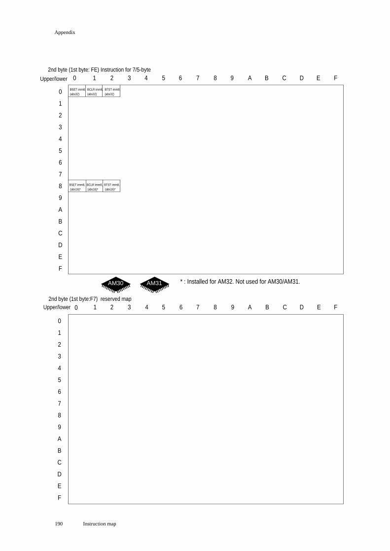
Appendix
Instruction map190
2nd byte (1st byte: FE) Instruction for 7/5-byte
Upper/lower
2nd byte (1st byte:F7) reserved mapUpper/lower
BSET imm8,(abs32)
BCLR imm8,(abs32)0
1
2
3
4
5
6
7
8
9
A
B
C
D
E
F
0
1
2
3
4
5
6
7
8
9
A
B
C
D
E
F
0 1 2 3 4 5 6 7 8 9 A B C D E F
0 1 2 3 4 5 6 7 8 9 A B C D E F
BTST imm8,(abs32)
BSET imm8,(abs16)*
BCLR imm8,(abs16)*
BTST imm8,(abs16)*
* : Installed for AM32. Not used for AM30/AM31.AM31AM30

5Index
192 Index
AADD Am,An ............................................. 46
Am,Dn ............................................. 46
Dm,Dn ............................................. 46
Dm,Dn ............................................. 46
imm16,An ....................................... 47
imm16,Dn ....................................... 47
imm16,SP ........................................ 47
imm32,An ....................................... 47
imm32,Dn ....................................... 47
imm32,SP ........................................ 47
imm8, An ......................................... 47
imm8,Dn ......................................... 47
imm8,SP .......................................... 47
ADDC Dm,Dn ............................................. 48
AND Dm,Dn ............................................. 59
imm16,Dn ....................................... 59
imm16,PSW .................................... 60
imm32,Dn ....................................... 59
imm8,Dn ......................................... 59
ASL Dm,Dn ............................................. 76
imm8,Dn ......................................... 77
ASL2 Dn .................................................... 78
ASR Dm,Dn ............................................. 70
Dn .................................................... 72
imm8,Dn ......................................... 71
BBCC label ................................................. 81
BCLR Dm,(An) .......................................... 68
imm8,(abs16) .................................. 69
imm8,(abs32) .................................. 69
imm8,(d8,An) .................................. 69
BCS label ................................................. 81
BEQ label ................................................. 81
BGE label ................................................. 81
BGT label ................................................. 81
BHI label ................................................. 81
BLE label ................................................. 81
BLS label ................................................. 81
BLT label ................................................. 81
BNC label ................................................. 81
BNE label ................................................. 81
BNS label ................................................. 81
BRA label ................................................. 81
BSET Dm,(An) .......................................... 66
imm8,(abs16) .................................. 67
imm8,(abs32) .................................. 67
imm8,(d8,An) ................................. 67
BTST imm16,Dn ....................................... 65
imm32,Dn ....................................... 65
imm8,(abs16) .................................. 65
imm8,(abs32) .................................. 65
imm8,(d8,An) ................................. 65
imm8,Dn ......................................... 65
BVC label ................................................ 81
BVS label ................................................ 81
CCALL label ................................................ 85
CALLS (An) ................................................. 87
label ................................................ 88
CLR Dn ................................................... 45
CMP Am,An ............................................ 58
Am,Dn ............................................ 58
Dm,An ............................................ 58
Dm,Dn ............................................ 58
imm16,An ....................................... 58
imm16,Dn ....................................... 58
imm32,An ....................................... 58
imm32,Dn ....................................... 58
imm8,An ......................................... 58
imm8,Dn ......................................... 58
DDIV Dm,Dn ............................................ 54
DIVU Dm,Dn ............................................ 55
EEXT Dn ................................................... 40
EXTB Dn ................................................... 41
EXTBU Dn ................................................... 42
EXTH Dn ................................................... 43
EXTHU Dn ................................................... 44
IINC Dn ................................................... 56
An ................................................... 56
INC4 An ................................................... 57
Index
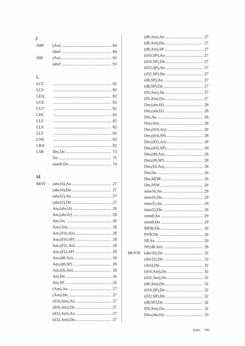
Index 193
JJMP (An) ................................................. 84
label ................................................ 84
JSR (An) ................................................. 92
label ................................................ 93
LLCC ........................................................ 82
LCS ........................................................ 82
LEQ ........................................................ 82
LGE ........................................................ 82
LGT ........................................................ 82
LHI ........................................................ 82
LLE ........................................................ 82
LLS ........................................................ 82
LLT ........................................................ 82
LNE ........................................................ 82
LRA ........................................................ 82
LSR Dm,Dn ............................................ 73
Dn ................................................... 75
imm8,Dn ......................................... 74
MMOV (abs16),An ...................................... 27
(abs16),Dn ...................................... 27
(abs32),An ...................................... 27
(abs32),Dn ...................................... 27
Am,(abs16) ..................................... 28
Am,(abs32) ..................................... 28
Am,An ............................................ 26
Am,(An) .......................................... 28
Am,(d16,An) ................................... 28
Am,(d16,SP) ................................... 28
Am,(d32,An) ................................... 28
Am,(d32,SP) ................................... 28
Am,(d8,An) ..................................... 28
Am,(d8,SP) ..................................... 28
Am,(Di,An) ..................................... 28
Am,Dn ............................................ 26
Am,SP ............................................. 26
(Am),An.......................................... 27
(Am),Dn.......................................... 27
(d16,Am),An................................... 27
(d16,Am),Dn................................... 27
(d32,Am),An................................... 27
(d32,Am),Dn................................... 27
(d8,Am),An..................................... 27
(d8,Am),Dn..................................... 27
(d8,Am),SP ..................................... 27
(d16,SP),An .................................... 27
(d16,SP),Dn .................................... 27
(d32,SP),An .................................... 27
(d32,SP),Dn .................................... 27
(d8,SP),An ...................................... 27
(d8,SP),Dn ...................................... 27
(Di,Am),An..................................... 27
(Di,Am),Dn..................................... 27
Dm,(abs16) ..................................... 28
Dm,(abs32) ..................................... 28
Dm,An ............................................ 26
Dm,(An) .......................................... 28
Dm,(d16,An) ................................... 28
Dm,(d16,SP) ................................... 28
Dm,(d32,An) ................................... 28
Dm,(d32,SP) ................................... 28
Dm,(d8,An) ..................................... 28
Dm,(d8,SP) ..................................... 28
Dm,(Di,An) ..................................... 28
Dm,Dn ............................................ 26
Dm,MDR ........................................ 26
Dm,PSW ......................................... 26
imm16,An ....................................... 29
imm16,Dn ....................................... 29
imm32,An ....................................... 29
imm32,Dn ....................................... 29
imm8,An ......................................... 29
imm8,Dn ......................................... 29
MDR,Dn ......................................... 26
PSW,Dn .......................................... 26
SP,An .............................................. 26
SP,(d8,An) ....................................... 28
MOVB (abs16),Dn ...................................... 32
(abs32),Dn ...................................... 32
(Am),Dn.......................................... 32
(d16,Am),Dn................................... 32
(d32,Am),Dn................................... 32
(d8,Am),Dn..................................... 32
(d16,SP),Dn .................................... 32
(d32,SP),Dn .................................... 32
(d8,SP),Dn ...................................... 32
(Di,Am),Dn..................................... 32
Dm,(abs16) ..................................... 33
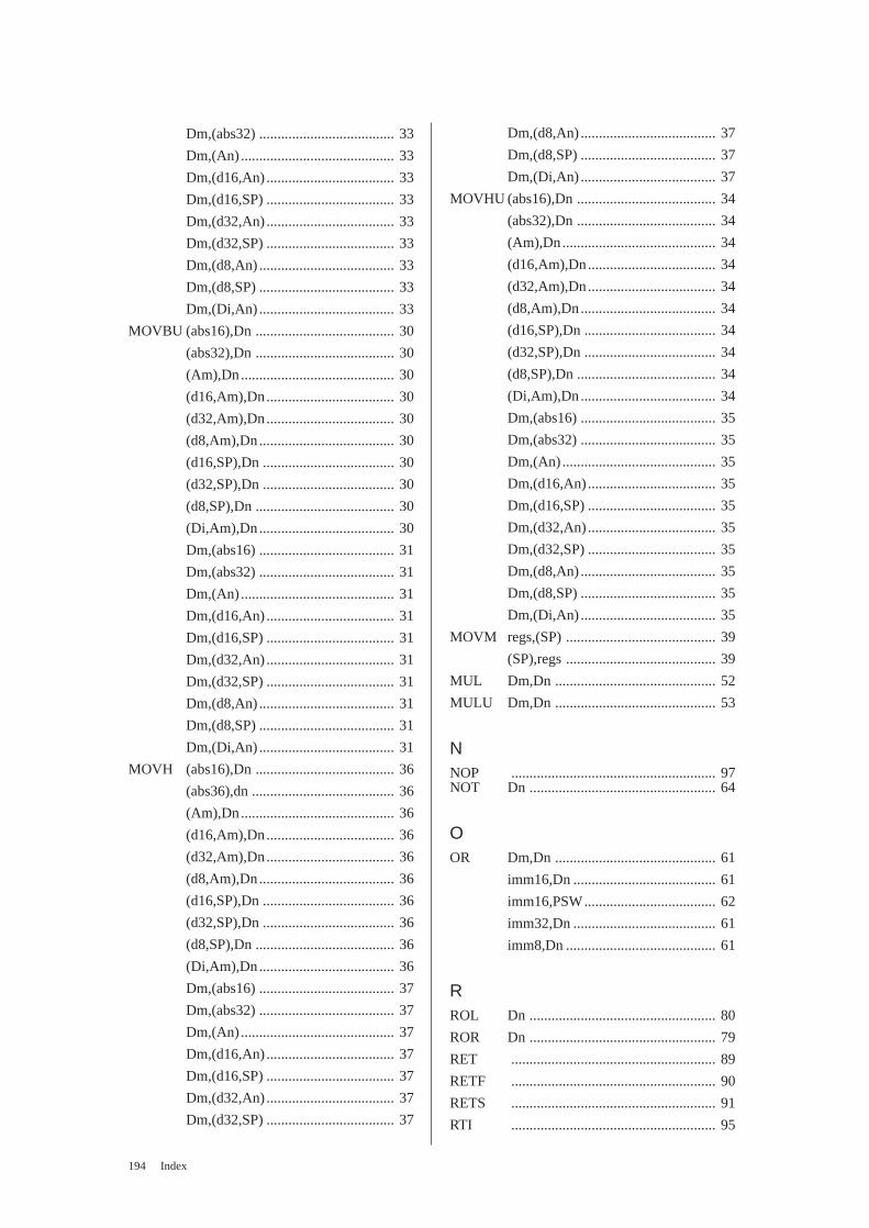
194 Index
Dm,(abs32) ..................................... 33
Dm,(An) .......................................... 33
Dm,(d16,An) ................................... 33
Dm,(d16,SP) ................................... 33
Dm,(d32,An) ................................... 33
Dm,(d32,SP) ................................... 33
Dm,(d8,An) ..................................... 33
Dm,(d8,SP) ..................................... 33
Dm,(Di,An) ..................................... 33
MOVBU (abs16),Dn ...................................... 30
(abs32),Dn ...................................... 30
(Am),Dn.......................................... 30
(d16,Am),Dn................................... 30
(d32,Am),Dn................................... 30
(d8,Am),Dn..................................... 30
(d16,SP),Dn .................................... 30
(d32,SP),Dn .................................... 30
(d8,SP),Dn ...................................... 30
(Di,Am),Dn..................................... 30
Dm,(abs16) ..................................... 31
Dm,(abs32) ..................................... 31
Dm,(An) .......................................... 31
Dm,(d16,An) ................................... 31
Dm,(d16,SP) ................................... 31
Dm,(d32,An) ................................... 31
Dm,(d32,SP) ................................... 31
Dm,(d8,An) ..................................... 31
Dm,(d8,SP) ..................................... 31
Dm,(Di,An) ..................................... 31
MOVH (abs16),Dn ...................................... 36
(abs36),dn ....................................... 36
(Am),Dn.......................................... 36
(d16,Am),Dn................................... 36
(d32,Am),Dn................................... 36
(d8,Am),Dn..................................... 36
(d16,SP),Dn .................................... 36
(d32,SP),Dn .................................... 36
(d8,SP),Dn ...................................... 36
(Di,Am),Dn..................................... 36
Dm,(abs16) ..................................... 37
Dm,(abs32) ..................................... 37
Dm,(An) .......................................... 37
Dm,(d16,An) ................................... 37
Dm,(d16,SP) ................................... 37
Dm,(d32,An) ................................... 37
Dm,(d32,SP) ................................... 37
Dm,(d8,An) ..................................... 37
Dm,(d8,SP) ..................................... 37
Dm,(Di,An) ..................................... 37
MOVHU (abs16),Dn ...................................... 34
(abs32),Dn ...................................... 34
(Am),Dn.......................................... 34
(d16,Am),Dn................................... 34
(d32,Am),Dn................................... 34
(d8,Am),Dn..................................... 34
(d16,SP),Dn .................................... 34
(d32,SP),Dn .................................... 34
(d8,SP),Dn ...................................... 34
(Di,Am),Dn..................................... 34
Dm,(abs16) ..................................... 35
Dm,(abs32) ..................................... 35
Dm,(An) .......................................... 35
Dm,(d16,An) ................................... 35
Dm,(d16,SP) ................................... 35
Dm,(d32,An) ................................... 35
Dm,(d32,SP) ................................... 35
Dm,(d8,An) ..................................... 35
Dm,(d8,SP) ..................................... 35
Dm,(Di,An) ..................................... 35
MOVM regs,(SP) ......................................... 39
(SP),regs ......................................... 39
MUL Dm,Dn ............................................ 52
MULU Dm,Dn ............................................ 53
NNOP ........................................................ 97NOT Dn ................................................... 64
OOR Dm,Dn ............................................ 61
imm16,Dn ....................................... 61
imm16,PSW.................................... 62
imm32,Dn ....................................... 61
imm8,Dn ......................................... 61
RROL Dn ................................................... 80
ROR Dn ................................................... 79
RET ........................................................ 89
RETF ........................................................ 90
RETS ........................................................ 91
RTI ........................................................ 95
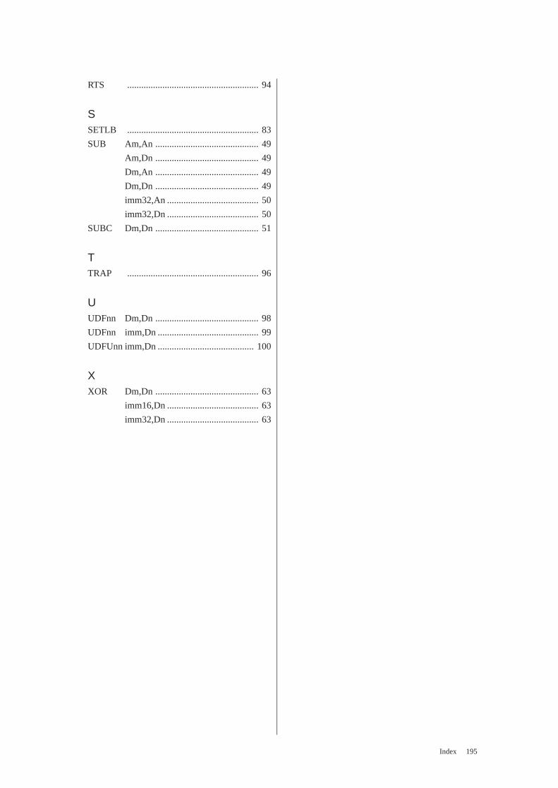
Index 195
RTS ........................................................ 94
SSETLB ........................................................ 83
SUB Am,An ............................................ 49
Am,Dn ............................................ 49
Dm,An ............................................ 49
Dm,Dn ............................................ 49
imm32,An ....................................... 50
imm32,Dn ....................................... 50
SUBC Dm,Dn ............................................ 51
TTRAP ........................................................ 96
UUDFnn Dm,Dn ............................................ 98
UDFnn imm,Dn ........................................... 99
UDFUnn imm,Dn ......................................... 100
XXOR Dm,Dn ............................................ 63
imm16,Dn ....................................... 63
imm32,Dn ....................................... 63

Issued by Matsushita Electric Industrial Co., Ltd.
Matsushita Electric Industrial Co., Ltd.
MN1030/MN103S SeriesInstruction Manual
January, 2003 4th Edition
Semiconductor Company, Matsushita Electric Industrial Co., Ltd.Nagaokakyo, Kyoto 617-8520, Japan
Tel: (075) 951-8151http://www.panasonic.co.jp/semicon/
SALES OFFICES■ NORTH AMERICA
● U.S.A. Sales Office:Panasonic Industrial Company [PIC]• New Jersey Office:Two Panasonic Way Secaucus, New Jersey 07094 U.S.A.
Tel: 1-201-348-5257 Fax:1-201-392-4652• Chicago Office:1707 N. Randall Road Elgin, Illinois 60123-7847 U.S.A.
Tel: 1-847-468-5720 Fax:1-847-468-5725• Milpitas Office:1600 McCandless Drive Milpitas, California 95035 U.S.A.
Tel: 1-408-942-2912 Fax:1-408-946-9063• Atlanta Office:1225 Northbrook Parkway Suite 1-151 Suwanee, GA30024 U.S.A.
Tel: 1-770-338-6953 Fax:1-770-338-6849• San Diego Office:9444 Balboa Avenue, Suite 185, San Diego, California92123 U.S.A.
Tel: 1-619-503-2903 Fax:1-858-715-5545● Canada Sales Office:
Panasonic Canada Inc. [PCI]5770 Ambler Drive 27 Mississauga, Ontario, L4W 2T3CANADA
Tel: 1-905-238-2315 Fax:1-905-238-2414■ LATIN AMERICA
● Mexico Sales Office:Panasonic de Mexico, S.A. de C.V. [PANAMEX]Amores 1120 Col. Del Valle Delegacion Benito JuarezC.P. 03100 Mexico, D.F. MEXICO
Tel: 52-5-488-1000 Fax:52-5-488-1073• Guadalajara Office:SUCURSAL GUADALAJARAAv. Lazaro Cardenas 2305 Local G-102 Plaza ComercialAbastos; Col. Las Torres Guadalajara, Jal. 44920MEXICO
Tel: 52-3-671-1205 Fax:52-3-671-1256● Brazil Sales Office:
Panasonic do Brasil Ltda. [PANABRAS]Caixa Postal 1641, Sao Jose dos Campos, Estado de SaoPaulo
Tel: 55-12-335-9000 Fax:55-12-331-3789■ EUROPE
● Europe Sales Office:Panasonic Industrial Europe GmbH [PIE]• U.K. Sales Office:Willoughby Road, Bracknell, Berks., RG12 8FP,THE UNITED KINGDOM
Tel: 44-1344-85-3671 Fax:44-1344-85-3853• Germany Sales Office:Hans-Pinsel-Strasse 2 85540 Haar, GERMANY
Tel: 49-89-46159-119 Fax:49-89-46159-195■ ASIA
● Singapore Sales Office:Panasonic Semiconductor of South Asia [PSSA]300 Beach Road, #16-01, The Concourse, Singapore199555 THE REPUBLIC OF SINGAPORE
Tel: 65-6390-3688 Fax:65-6390-3689● Malaysia Sales Office:
Panasonic Industrial Company (M) Sdn. Bhd. [PICM]• Head Office:Tingkat 16B, Menara PKNS Petaling Jaya, No.17, JalanYong Shook Lin 46050 Petaling Jaya, Selangor DarulEhsan, MALAYSIA
Tel: 60-3-7951-6601 Fax:60-3-7954-5968
• Penang Office:Suite 20-07,20th Floor, MWE Plaza, No.8, LebuhFarquhar,10200 Penang, MALAYSIA
Tel: 60-4-201-5113 Fax:60-4-261-9989• Johore Sales Office:Menara Pelangi, Suite8.3A, Level8, No.2, Jalan KuningTaman Pelangi, 80400 Johor Bahru, Johor, MALAYSIA
Tel: 60-7-331-3822 Fax:60-7-355-3996● Thailand Sales Office:
Panasonic Industrial (THAILAND) Ltd. [PICT]252-133 Muang Thai-Phatra Complex Building, 31st Fl.Rachadaphisek Rd., Huaykwang, Bangkok 10320,THAILAND
Tel: 66-2-693-3428 Fax:66-2-693-3422● Philippines Sales Office: [PISP]
Panasonic Indsutrial Sales Philippines Division ofMatsushita Electric Philippines Corporation102 Laguna Boulevard,Bo.Don Jose Laguna Technopark,Santa. Rosa, Laguna 4026 PHILIPPINES
Tel: 63-2-520-8615 Fax:63-2-520-8629● India Sales Office:
National Panasonic India Ltd. [NPI]E Block, 510, International Trade Tower Nehru Place, NewDelhi_110019 INDIA
Tel: 91-11-629-2870 Fax:91-11-629-2877● Indonesia Sales Office:
P.T.MET & Gobel [M&G]JL. Dewi Sartika (Cawang 2) Jakarta 13630, INDONESIA
Tel: 62-21-801-5666 Fax:62-21-801-5675● China Sales Office:
Panasonic Industrial (Shanghai) Co., Ltd. [PI(SH)]Floor 6, Zhong Bao Mansion, 166 East Road Lujian Zui,PU Dong New District, Shanghai, 200120 CHINA
Tel: 86-21-5866-6114 Fax:86-21-5866-8000Panasonic Industrial (Tianjin) Co., Ltd. [PI(TJ)]Room No.1001, Tianjin International Building 75, NanjinRoad, Tianjin 300050, CHINA
Tel: 86-22-2313-9771 Fax:86-22-2313-9770Panasonic SH Industrial Sales (Shenzhen) Co., Ltd.
[PSI(SZ)]7A-107, International Bussiness & Exhibition Centre,Futian Free Trade Zone, Shenzhen 518048, CHINA
Tel: 86-755-8359-8500 Fax:86-755-8359-8516Panasonic Shun Hing Industrial Sales (Hong Kong)Co., Ltd. [PSI(HK)]11th Floor, Great Eagle Center 23 Harbour Road,Wanchai, HONG KONG
Tel: 852-2529-7322 Fax:852-2865-3697● Taiwan Sales Office:
Panasonic Industrial Sales (Taiwan) Co.,Ltd. [PIST]• Head Office:6F, 550, Sec. 4, Chung Hsiao E. RD. Taipei, 110, TAIWAN
Tel: 886-2-2757-1900 Fax:886-2-2757-1906• Kaohsiung Office:6th Floor, Hsin Kong Bldg. No.251, Chi Hsien 1st RoadKaohsiung 800, TAIWAN
Tel: 886-7-346-3815 Fax:886-7-236-8362● Korea Sales Office:
Panasonic Industrial Korea Co., Ltd. [PIKL]Kukje Center Bldg. 11th Fl., 191 Hangangro 2ga,Youngsan-ku, Seoul 140-702, KOREA
Tel: 82-2-795-9600 Fax:82-2-795-1542
Printed in JAPAN Matsushita Electric Industrial Co., Ltd. 2003220103