Embed Size (px)
Citation preview

Outline
• Target applications for the Millimeter-wave frequency band
• Silicon technologies to address mmW complete solutions– Active devices on bulk and SOI technologies– Passive devices
• Silicon integrated solutions for mmW circuits– LNA mmW designs– Down-conversion mixers for mmW– Voltage controlled oscillators for mmW– Power amplifiers for mmW– mmW Assembly
•• ConclusionsConclusions
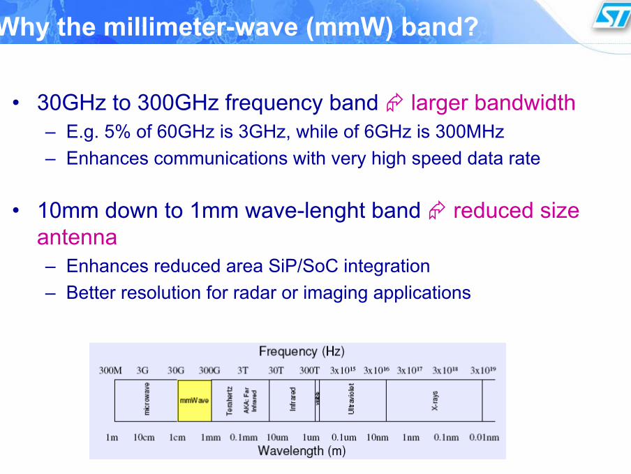
Why the millimeter-wave (mmW) band?
• 30GHz to 300GHz frequency band larger bandwidth– E.g. 5% of 60GHz is 3GHz, while of 6GHz is 300MHz– Enhances communications with very high speed data rate
• 10mm down to 1mm wave-lenght band reduced size antenna– Enhances reduced area SiP/SoC integration– Better resolution for radar or imaging applications
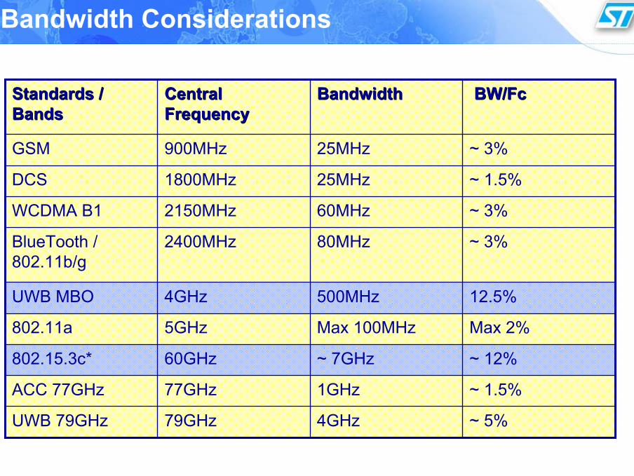
Bandwidth Considerations
~ 5%4GHz79GHzUWB 79GHz
~ 1.5%1GHz77GHzACC 77GHz
~ 12%~ 7GHz60GHz802.15.3c*
Max 2%Max 100MHz5GHz802.11a
12.5%500MHz4GHzUWB MBO
~ 3%80MHz2400MHzBlueTooth / 802.11b/g
~ 3%60MHz2150MHzWCDMA B1
~ 1.5%25MHz1800MHzDCS
~ 3%25MHz900MHzGSM
BW/BW/FcFcBandwidthBandwidthCentral Central FrequencyFrequency
Standards / Standards / BandsBands
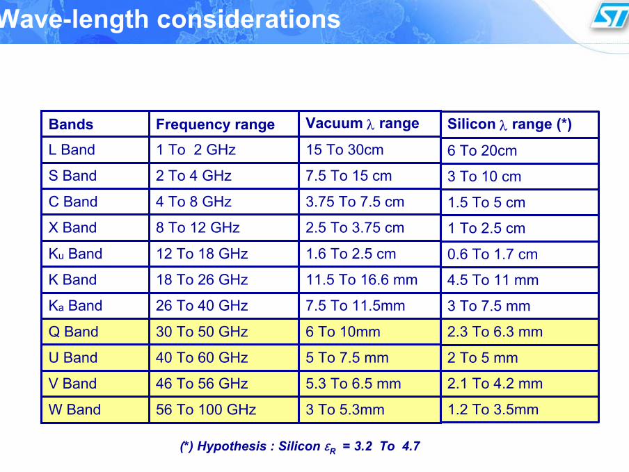
Wave-length considerations
3 To 5.3mm56 To 100 GHzW Band
5.3 To 6.5 mm46 To 56 GHzV Band
5 To 7.5 mm40 To 60 GHzU Band
6 To 10mm30 To 50 GHzQ Band
7.5 To 11.5mm26 To 40 GHzKa Band
11.5 To 16.6 mm18 To 26 GHzK Band
1.6 To 2.5 cm12 To 18 GHzKu Band
2.5 To 3.75 cm8 To 12 GHzX Band
3.75 To 7.5 cm4 To 8 GHzC Band
7.5 To 15 cm2 To 4 GHzS Band
15 To 30cm1 To 2 GHzL Band
Vacuum λ range Frequency rangeBands
1.2 To 3.5mm
2.1 To 4.2 mm
2 To 5 mm
2.3 To 6.3 mm
3 To 7.5 mm
4.5 To 11 mm
0.6 To 1.7 cm
1 To 2.5 cm
1.5 To 5 cm
3 To 10 cm
6 To 20cm
Silicon λ range (*)
(*) Hypothesis : Silicon εR = 3.2 To 4.7

mmW Communications Application Fields at a Glance
• High data-rate communications– Last Inch applications (57 to 66GHz bands)
• Wireless HDMI video streaming• Short Range Ultra fast file transfer
– Last Mile applications (71-76GHz, 81-86GHz licensed E-bands)• Telecom backhauls
• Low data-rate communications (94GHz, >100GHz bands)– Sensor network applications
• Automotive applications – Radar items:
• Long range radar (ACC) (76-77GHz bands)• Short range radar (Stop & Go) (77-81GHz bands)
– Ground to vehicle and vehicle to vehicle links (see HDR communications)
• Optical communications• Chip to chip wireless communications

Example 1: Indoor network scenario and interfacing to the outdoor network
IDU+MODEM
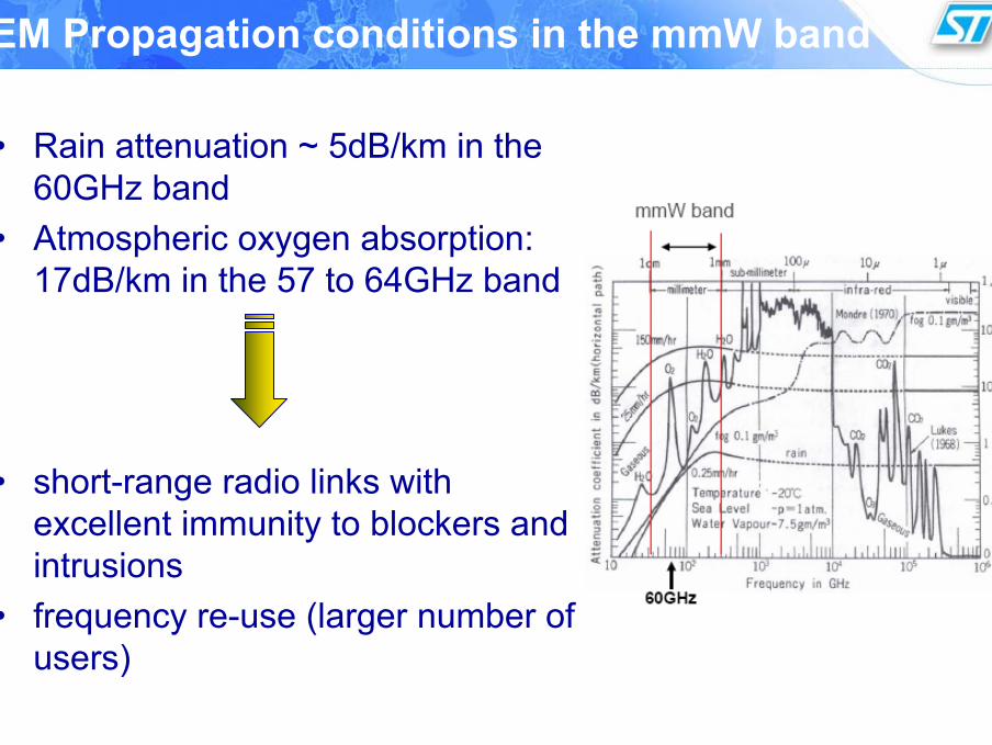
EM Propagation conditions in the mmW band
• Rain attenuation ~ 5dB/km in the 60GHz band
• Atmospheric oxygen absorption: 17dB/km in the 57 to 64GHz band
• short-range radio links with excellent immunity to blockers and intrusions
• frequency re-use (larger number of users)
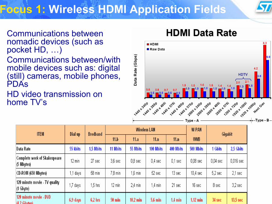
Focus 1: Wireless HDMI Application Fields
• Communications between nomadic devices (such as pocket HD, …)
• Communications between/with mobile devices such as: digital (still) cameras, mobile phones, PDAs
• HD video transmission on home TV’s
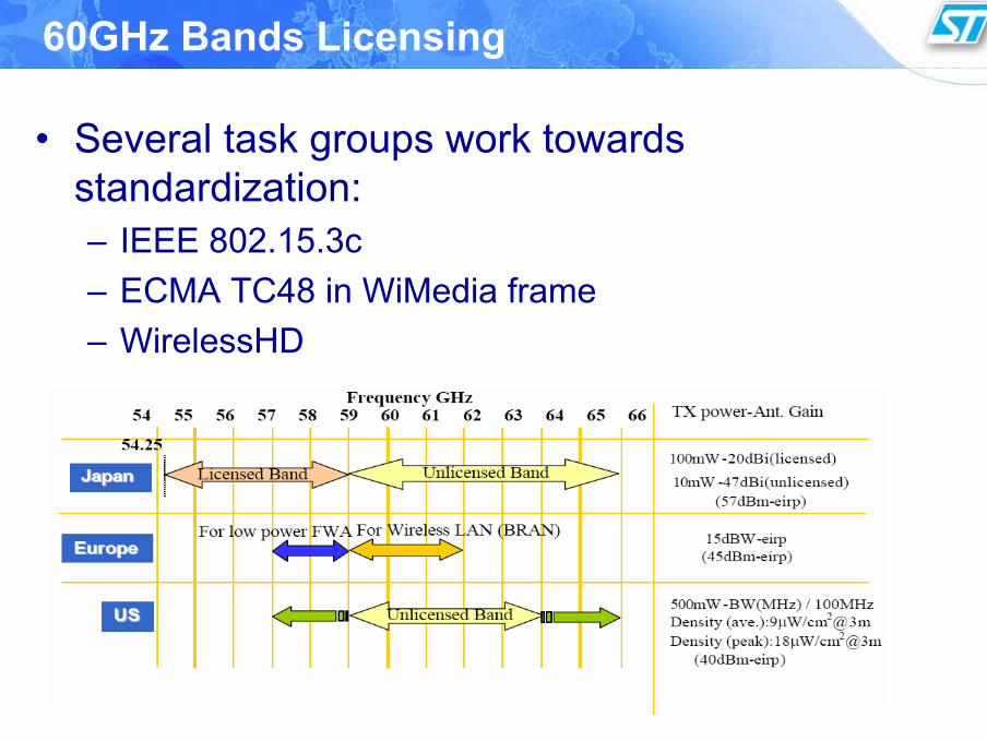
60GHz Bands Licensing
• Several task groups work towards standardization:– IEEE 802.15.3c– ECMA TC48 in WiMedia frame– WirelessHD
Group Forecasted by:
Characteristics Web link
IEEE 802.15.3c (TG3c)
May 2009 PHY layer Standard based on millimeter waves. Target band-pass is 1-2 Gbit/s
www.ieee802.org/15/pub/TG3c.html
ECMA –TC48 (ex TC32-TG20)
Mid 2009 PHY+MAC Standard, low power, data rate 2-10 Gbit/sretro-compatible with HDCP part of HDMI
www.ecma-international.org/memento/TC48-M.html
WiMedia Alliance which standardizes the UWB communications protocols. For the 60GHz band it is synchronized with TC48.
www.wimedia.org
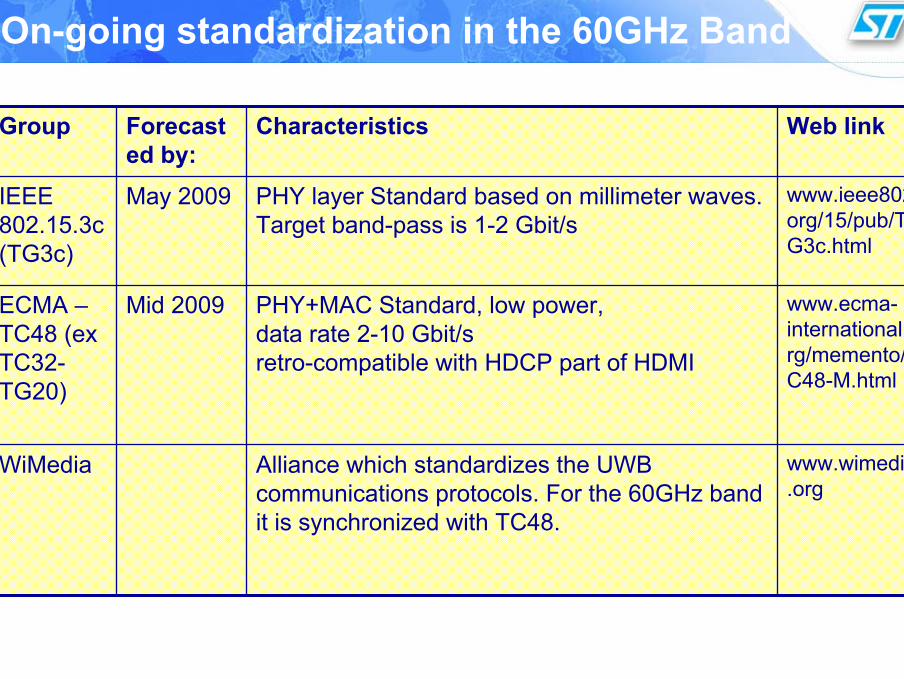
On-going standardization in the 60GHz Band
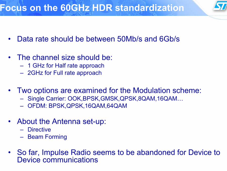
Focus on the 60GHz HDR standardization
• Data rate should be between 50Mb/s and 6Gb/s
• The channel size should be:– 1 GHz for Half rate approach– 2GHz for Full rate approach
• Two options are examined for the Modulation scheme:– Single Carrier: OOK,BPSK,GMSK,QPSK,8QAM,16QAM…– OFDM: BPSK,QPSK,16QAM,64QAM
• About the Antenna set-up:– Directive– Beam Forming
• So far, Impulse Radio seems to be abandoned for Device to Device communications
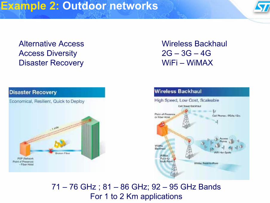
Example 2: Outdoor networks
Alternative AccessAccess DiversityDisaster Recovery
Wireless Backhaul2G – 3G – 4GWiFi – WiMAX
71 – 76 GHz ; 81 – 86 GHz; 92 – 95 GHz BandsFor 1 to 2 Km applications
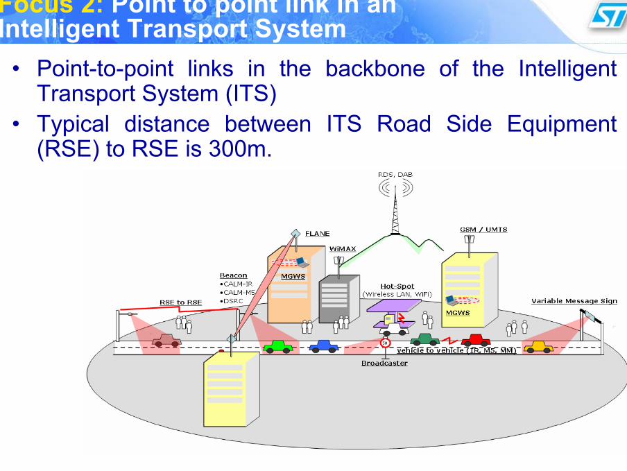
Focus 2: Point to point link in an Intelligent Transport System
• Point-to-point links in the backbone of the Intelligent Transport System (ITS)
• Typical distance between ITS Road Side Equipment (RSE) to RSE is 300m.
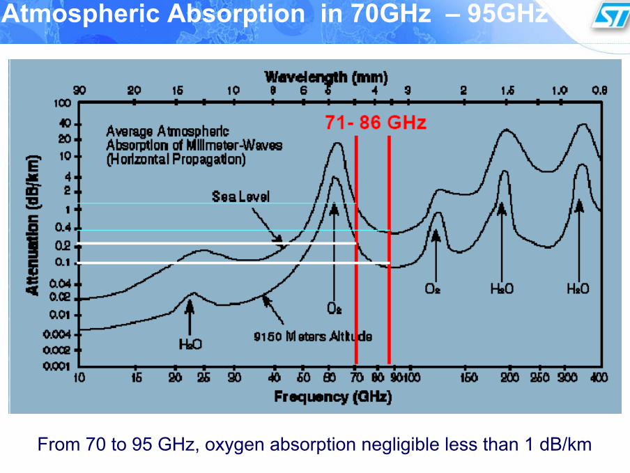
Atmospheric Absorption in 70GHz – 95GHz
From 70 to 95 GHz, oxygen absorption negligible less than 1 dB/km

Rain Losses in 70GHz – 95GHz
Light rain < 1 dB/kmHeavy rain = 10 dB/kmDownpour = 30 dB/km
Sand, dust, fog, snow, etc have no significant effect attenuation at mm-waves

Standardization for Outdoor Network
• US FCC Allowance:– 3 Allowed Bands:
• 71-76 GHz; 81-86 GHz ; 92-95 GHz– Emitted Isotropic Radiated Power:
• 55 dBW EIRP at 50 dB antenna gain • 41 dBW EIRP at 43 dB antenna gain
• European regulatory status:– 2 Bands approved by European regulators (EU and CEPT):
• 71-76 GHz; 81-86 GHz
• World Wide regulatory status:– Goal is worldwide common radio band Goal is worldwide common
radio band and spectrum rules.– Positive Feedback from Bahrain, Jordan, Australia, South Africa,
Ghana, Nigeria, India, China, Brazil, Mexico, Canada

Example 3: Automotive applications contributing to road safety
• For Safe speed & Safe following:– Communication technologies to improve
the detection, locating and evaluation of hazards
– New sensorial devices integrating obstacle detection and communication
• For Lateral Support & Driver Monitoring:
– Lane-keeping support system for situations with poor road and environmental conditions
• For Intersection Safety:– Concepts for sensors and
communication aimed to road markings and crossing traffic recognition
• For Vulnerable Road Users & Collision Mitigation:
– Active 3D sensor technology for pre-crash and blind spot surveillance
– Location and classification of obstacles (cars, pedestrians, bikes, etc.)
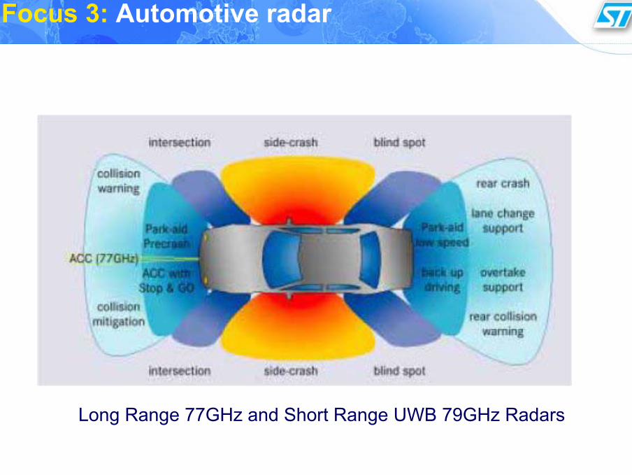
Focus 3: Automotive radar
Long Range 77GHz and Short Range UWB 79GHz Radars
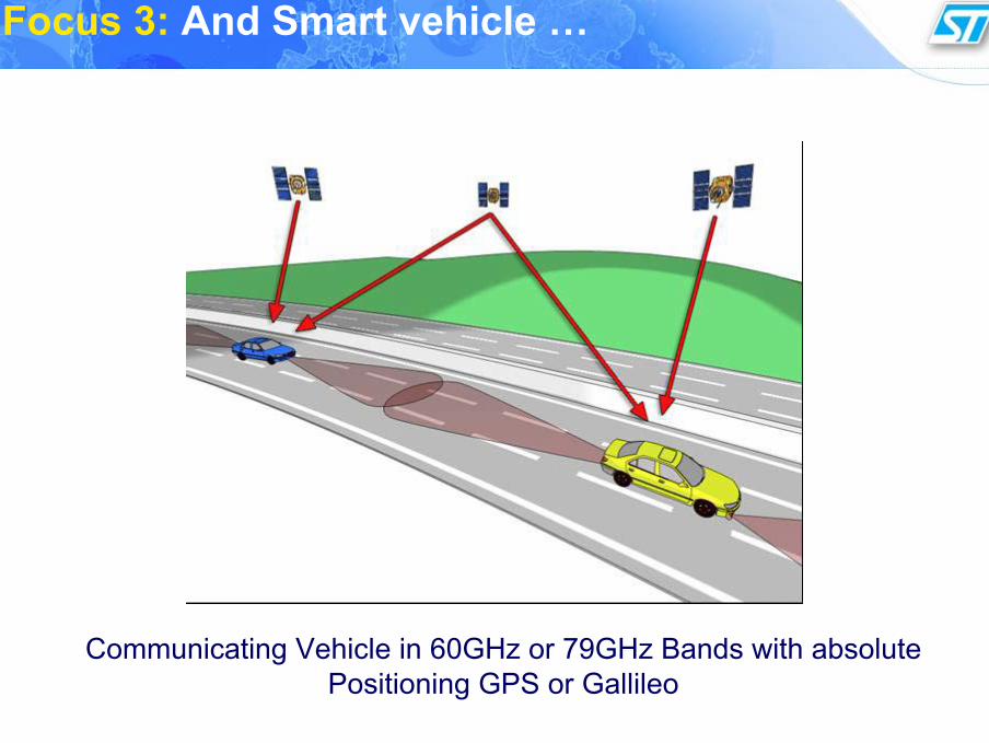
Focus 3: And Smart vehicle …
Communicating Vehicle in 60GHz or 79GHz Bands with absolute Positioning GPS or Gallileo
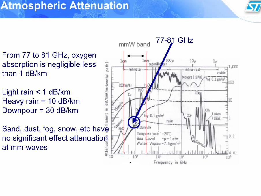
Atmospheric Attenuation
77-81 GHz
From 77 to 81 GHz, oxygen absorption is negligible less than 1 dB/km
Light rain < 1 dB/kmHeavy rain = 10 dB/kmDownpour = 30 dB/km
Sand, dust, fog, snow, etc have no significant effect attenuation at mm-waves
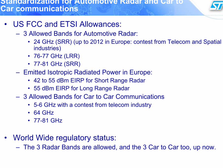
Standardization for Automotive Radar and Car to Car communications
• US FCC and ETSI Allowances:– 3 Allowed Bands for Automotive Radar:
• 24 GHz (SRR) (up to 2012 in Europe: contest from Telecom and Spatial industries)
• 76-77 GHz (LRR)• 77-81 GHz (SRR)
– Emitted Isotropic Radiated Power in Europe:• 42 to 55 dBm EIRP for Short Range Radar • 55 dBm EIRP for Long Range Radar
– 3 Allowed Bands for Car to Car Communications• 5-6 GHz with a contest from telecom industry• 64 GHz • 77-81 GHz
• World Wide regulatory status:– The 3 Radar Bands are allowed, and the 3 Car to Car too, up now.
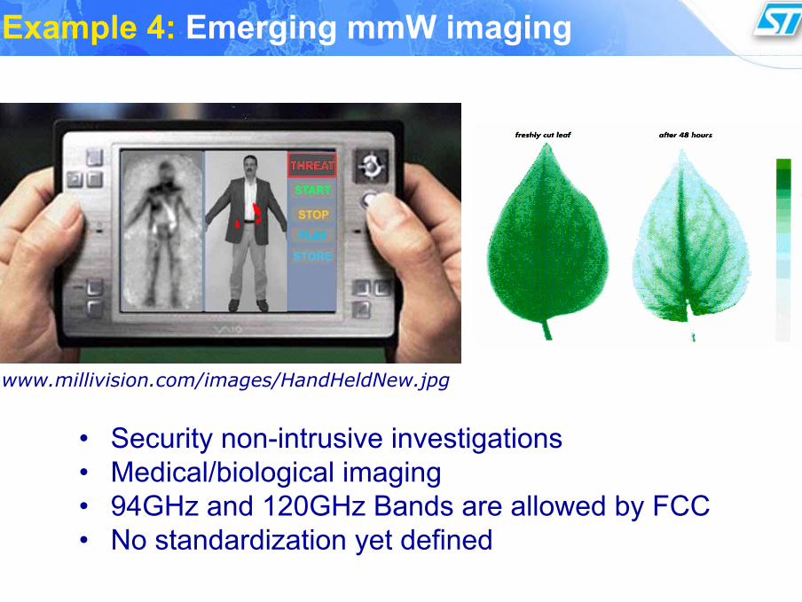
Example 4: Emerging mmW imaging
• Security non-intrusive investigations• Medical/biological imaging• 94GHz and 120GHz Bands are allowed by FCC• No standardization yet defined
www.millivision.com/images/HandHeldNew.jpg

Outline
• Target applications for the Millimeter-wave frequency band
• Silicon technologies to address mmW complete solutions– Active devices on bulk and SOI technologies– Passive devices
• Silicon integrated solutions for mmW circuits– LNA mmW designs– Down-conversion mixers for mmW– Voltage controlled oscillators for mmW– Power amplifiers for mmW– mmW Assembly
•• ConclusionsConclusions
How did we get to Silicon technologiesfor mmW designs?
• mmW market held since decades by the III-V semiconductors– Niche market w.r.t. the total market volume in all SC industry– III-V SC show high manufacturing cost and reduced integration
scale
• Since several years, full Silicon technologies become the technology integration platforms for mmW– Technical Enabler: the very high frequency performances of Si
active devices– Marketing Enabler: the need for low-cost consumer products in
the mmW frequency range

Silicon Technologies for mmW
• SiGe-C HBT:– 130nm HBT mmW technology.
• Nanometric CMOS Bulk:– 65 nm CMOS LP technology.
• SOI CMOS :– 65 nm CMOS LP HR SOI technology.
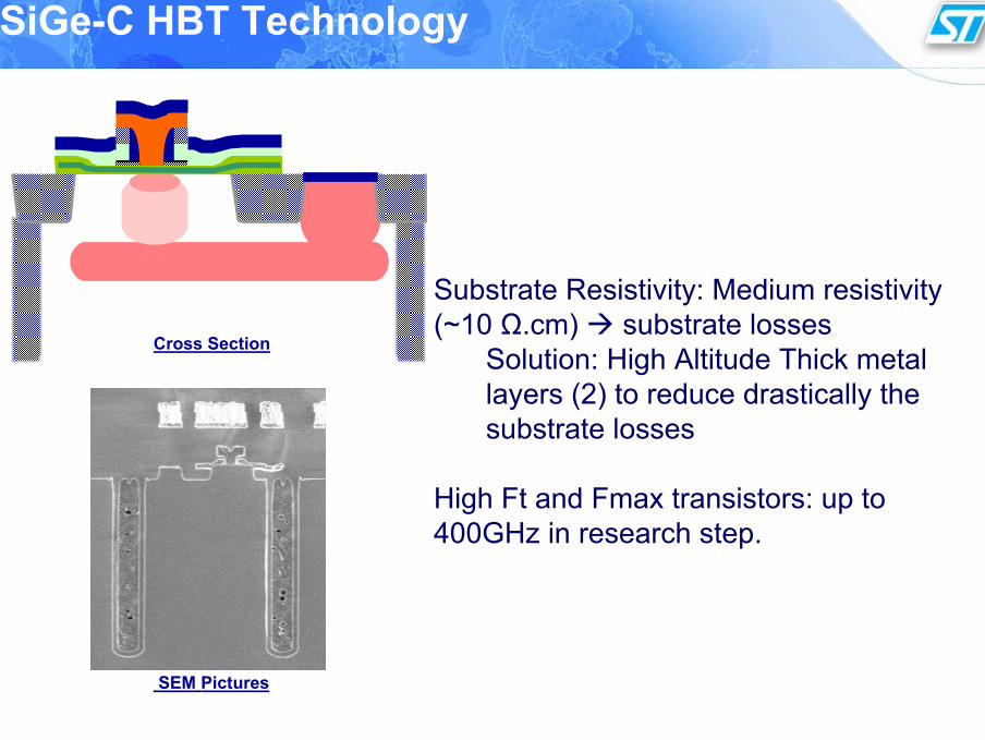
SiGe-C HBT Technology
Cross Section
SEM Pictures
Substrate Resistivity: Medium resistivity (~10 Ω.cm) substrate losses
Solution: High Altitude Thick metal layers (2) to reduce drastically the substrate losses
High Ft and Fmax transistors: up to 400GHz in research step.

130nm node SiGe:C HBT devices RF performances
• Devices developed on purpose for high frequency/high speed operation mode• High speed performance: fT>200GHz, fmax > 300GHz obtained with FSA E-B
architectures and HP collector• Advantages over CMOS 65nm node: lower 1/f noise, higher Zout, higher voltage
capability for a given speed• fmax has reduced sensitivity to layout parasitics
1 2 3 40
50
100
150
200
250
300
350
fT × BVCEO (GHz.V)
fT × BVCEO (GHz.V)
450
300
150
QSA-SP-LC / bulk (Prod) QSA-DP-HP / bulk (Prod) FSA-DP-HP / bulk (Devt) (Proto) FSA-DP-LC / bulk (Devt) FSA-DP-LC / SOI (Devt) (Proto)
f T (G
Hz)
BVCEO (V)4 5 6 7 8 9 10 11 12 13
0
50
100
150
200
250
300
350
fmax × BVCBO (GHz.V)
1800
14001000
QSA-SP-LC / bulk (Prod) QSA-DP-HP / bulk (Prod) FSA-DP-HP / bulk (Devt) (Proto) FSA-DP-LC / bulk (Devt) FSA-DP-LC / SOI (Devt) (Proto)
f max
(GH
z)
BVCBO (V)
P. Chevalier, et al., ESSCIRC 2006 workshop
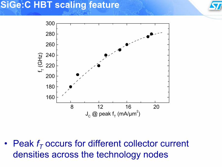
SiGe:C HBT scaling feature
• Peak fT occurs for different collector current densities across the technology nodes
8 12 16 20
160
180
200
220
240
260
280
300
f T (G
Hz)
JC @ peak fT (mA/µm2)

Thin CMOS SOI/bulk LP RF technologies
• Medium resistivity (~10 Ω.cm) in bulk technologies substrate losses • High resistivity (~1 KΩ.cm) cannot be used in case of bulk due to latch-up
issues– Solution: very good isolation and reduced losses thanks to High Resistivity substrates
possible only on SOI
Buried OxideSOI
> 1kOhm-cm Si
65nm LP SOI technology STMicroelectronics
STI
Bulk ~ 10 Ohm-cm
65nm LP Bulk technology STMicroelectronics
Courtesy to C. Raynaud, STMicroectronics & CEA
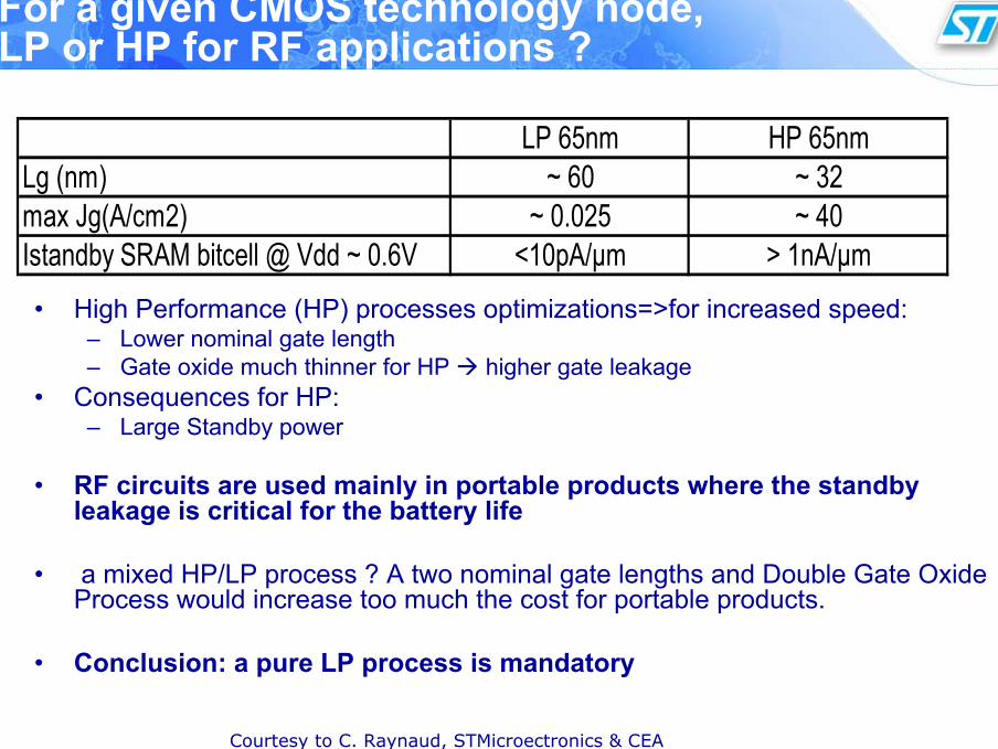
For a given CMOS technology node, LP or HP for RF applications ?
• High Performance (HP) processes optimizations=>for increased speed:– Lower nominal gate length – Gate oxide much thinner for HP higher gate leakage
• Consequences for HP:– Large Standby power
• RF circuits are used mainly in portable products where the standby leakage is critical for the battery life
• a mixed HP/LP process ? A two nominal gate lengths and Double Gate Oxide Process would increase too much the cost for portable products.
• Conclusion: a pure LP process is mandatory
LP 65nm HP 65nmLg (nm) ~ 60 ~ 32max Jg(A/cm2) ~ 0.025 ~ 40Istandby SRAM bitcell @ Vdd ~ 0.6V <10pA/µm > 1nA/µm
Courtesy to C. Raynaud, STMicroectronics & CEA
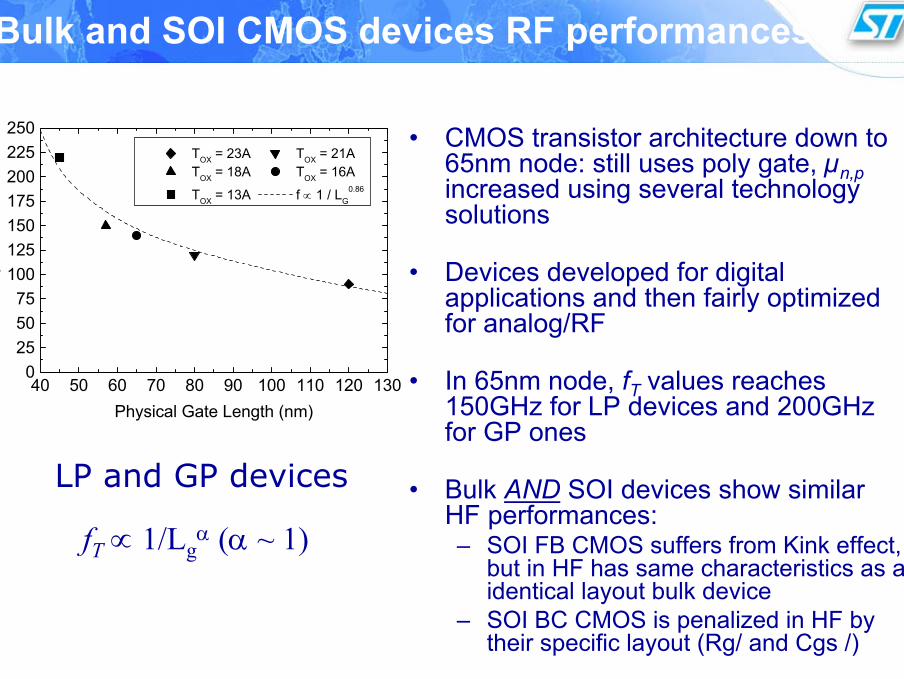
Bulk and SOI CMOS devices RF performances
• CMOS transistor architecture down to 65nm node: still uses poly gate, µn,pincreased using several technology solutions
• Devices developed for digital applications and then fairly optimized for analog/RF
• In 65nm node, fT values reaches 150GHz for LP devices and 200GHz for GP ones
• Bulk AND SOI devices show similar HF performances:– SOI FB CMOS suffers from Kink effect,
but in HF has same characteristics as a identical layout bulk device
– SOI BC CMOS is penalized in HF by their specific layout (Rg/ and Cgs /)
40 50 60 70 80 90 100 110 120 1300
255075
100125150175200225250
TOX = 23A TOX = 21A TOX = 18A TOX = 16A
TOX = 13A f ∝ 1 / LG0.86
f T (G
Hz)
Physical Gate Length (nm)
LP and GP devices
fT ∝ 1/Lgα (α ~ 1)

Evolution of fT through CMOS technology nodes several foundries
0
50
100
150
200
250
300
350
400
450
0 20 40 60 80 100
Physical Gate Length (nm)
f T [G
Hz]
ITRS roadmap 2006
CMOS SOI PD 130 IBM
CMOS SOI PD DTMOS 130 Fujitsu
CMOS SOI LP PD 130 ST
CMOS SOI HP 90 IBM
CMOS SOI HP 65 IBM
CMOS 65 Intel
CMOS SOI LP 65 ST
CMOS LP 65 ST
CMOS SOI HP 65 IBM
CMOS LP 45 ST
CMOS 45 IBM
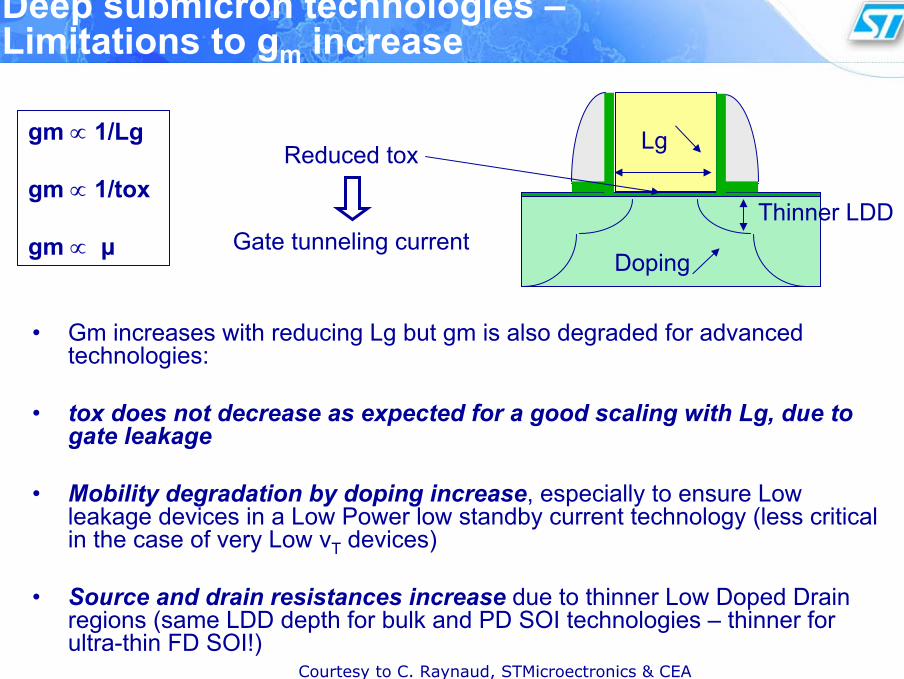
Deep submicron technologies –Limitations to gm increase
• Gm increases with reducing Lg but gm is also degraded for advanced technologies:
• tox does not decrease as expected for a good scaling with Lg, due to gate leakage
• Mobility degradation by doping increase, especially to ensure Low leakage devices in a Low Power low standby current technology (less critical in the case of very Low vT devices)
• Source and drain resistances increase due to thinner Low Doped Drain regions (same LDD depth for bulk and PD SOI technologies – thinner for ultra-thin FD SOI!)
gm ∝ 1/Lg
gm ∝ 1/tox
gm ∝ µ
Reduced tox
Gate tunneling currentDoping
Lg
Thinner LDD
Courtesy to C. Raynaud, STMicroectronics & CEA
Deep submicron technologies –Techniques to increase gm
• different “strain techniques” to increase mobility : Stress Memory Techniques (SMT), SiGe source-drain, stress liners, …
• use 45° rotated substrate (but valid only to increase mobility of PMOS)
• high K to limit gate leakage and decrease effective electrical gate oxide
• ultra thin SOI film to reduce doping level (vT definition by metal gate work-function) but gate material issue to get low vT and high vT at the same time and influence of ultra thin SOI film + high k on mobility and low frequency noise not yet well known
Courtesy to C. Raynaud, STMicroectronics & CEA

Bulk and SOI CMOS devices: fmax feature
0
100
200
300
400
500
600
700
0 20 40 60 80 100
Physical Gate Length (nm)
f max
[GH
z]
ITRS roadmap 2006
CMOS SOI PD 130 IBM
CMOS SOI PD DTMOS 130Fujitsu CMOS SOI LP PD 130 ST
CMOS SOI HP 90 IBM
CMOS SOI HP 65 IBM
CMOS 65 Intel
CMOS SOI LP 65 ST
CMOS LP 65 ST
CMOS 45 IBM

Influence of MOS transistor layout over fT and fmax parameters
• Optimal Wfinger ≤ 5µm• Double sided gate access
0
40
80
120
160
200
10 100Ids(m A)
f T (GHz)
0
40
80
120
160
200fmax(GHz)
Ft 8*(2*5*0.12) 2GA
Ft 8*(2*5*0.12)
Ft 2*(2*20*0.12)
Ft 8*(1*10*0.12)
Fmax 8*(2*5*0.12) 2GA
Fmax 8*(2*5*0.12)
Fmax 2*(2*20*0.12)
Fmax 8*(1*10*0.12)
fmax with 2 gate access, Wf = 5µm
fmax with different Wf
NMOS, Lpoly 90nm
130nm SOI process STMicroelectronics
Wf=20µm
Wf=5µm Wf=10µm
Transistor size: n*(Nf*Wf*Lg) in µm
n = number of transistor cells in parallel
Wf = finger width
Nf = number of transistor fingers per cell
Lg = gate length
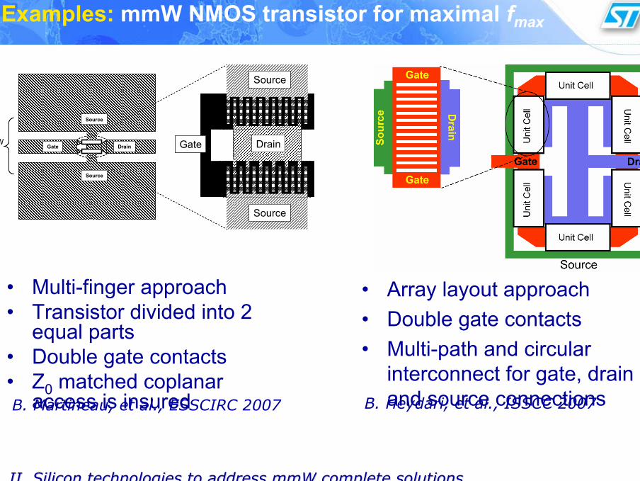
Examples: mmW NMOS transistor for maximal fmax
• Multi-finger approach• Transistor divided into 2
equal parts• Double gate contacts• Z0 matched coplanar
access is insured
CPW
Source
Source
DrainGate
Source
Source
DrainGate
Source
Source
DrainGate
Source
Source
DrainGate
• Array layout approach• Double gate contacts• Multi-path and circular
interconnect for gate, drain and source connectionsB. Martineau, et al., ESSCIRC 2007 B. Heydari, et al., ISSCC 2007
II. Silicon technologies to address mmW complete solutionsII. Silicon technologies to address mmW complete solutions

Bulk and SOI CMOS devices: NFmin feature
• NFmin is a linear function of frequency – it is a very difficult measurement in terms of accuracy (de – embedding is very complex in high frequency range)
• NFmin is degraded by high gate & source resistance => NFmin is dependent on layout
• No difference between bulk and SOI for same parasitic resistances and same gm
00,20,40,60,8
11,2
0 10 20 30f (GHz)
NFm
in(d
B) SOI PD, 65nm LP,
ST
bulk 45nm, IBM,VLSI07
ITRS L = 45nm@5GHz
ITRS L = 65nm@5GHz
Courtesy to C. Raynaud, STMicroectronics & CEA
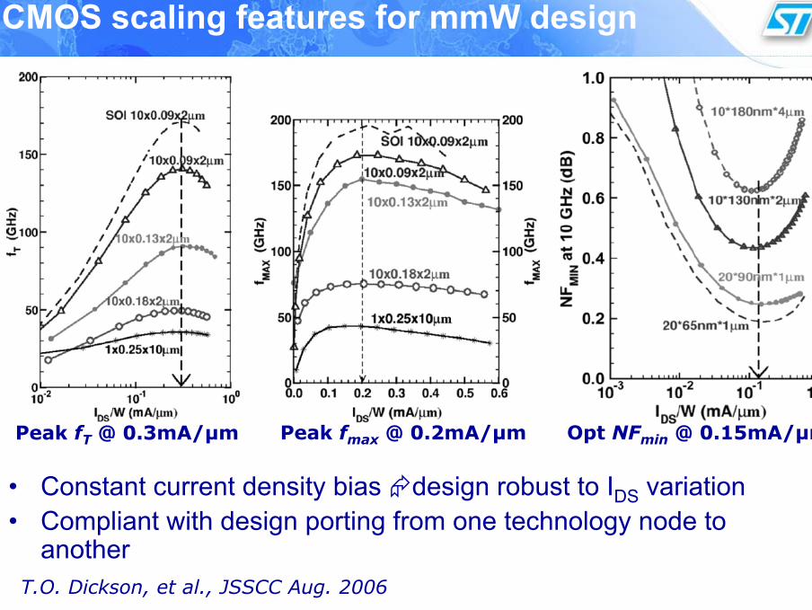
CMOS scaling features for mmW design
• Constant current density bias design robust to IDS variation• Compliant with design porting from one technology node to
another
Peak fT @ 0.3mA/µm Peak fmax @ 0.2mA/µm Opt NFmin @ 0.15mA/µm
T.O. Dickson, et al., JSSCC Aug. 2006
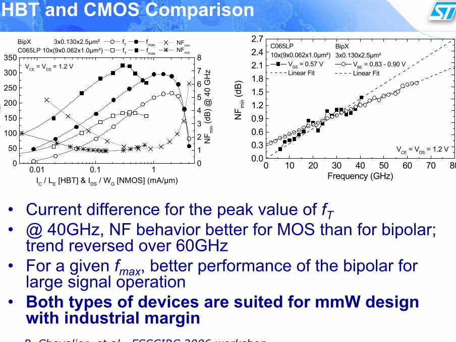
HBT and CMOS Comparison
• Current difference for the peak value of fT• @ 40GHz, NF behavior better for MOS than for bipolar;
trend reversed over 60GHz• For a given fmax, better performance of the bipolar for
large signal operation• Both types of devices are suited for mmW design
with industrial margin
0.01 0.1 10
50
100
150
200
250
300
350VCE = VDS = 1.2 V
BipX 3x0.130x2.5µm² fT fmax
C065LP 10x(9x0.062x1.0µm²) fT fmax
f T & f m
ax (G
Hz)
IC / LE [HBT] & IDS / WG [NMOS] (mA/µm)
0
1
2
3
4
5
6
7
8
NFmin NFmin
NF m
in (d
B) @
40
GH
z
0 10 20 30 40 50 60 70 800.00.30.60.91.21.51.82.12.42.7
VCE = VDS = 1.2 V
C065LP 10x(9x0.062x1.0µm²)
VGS = 0.57 V Linear Fit
NF m
in (d
B)
Frequency (GHz)
BipX3x0.130x2.5µm²
VBE = 0.83 - 0.90 V Linear Fit
P. Chevalier, et al., ESSCIRC 2006 workshop

BEOL evolution through technology nodes
• General trend: when moving from one technology node to another – vertical shrink of Me and dielectric thickness – reduction of the Me pitch
• Consequences:– Lumped elements (inductors): larger ohmic and substrate losses– Distributed elements (Tlines): attenuation constant degradation
• Possible solutions:– Use mmW dedicated BEOL (e.g. 3 thick Me layers + thick IMD)
drawback: application dedicated process– Use digital BEOL with max number of Me layers (e.g. 10 Me layers)
drawback: cost– Increase the substrate resistivity (e.g SOI HR)
drawback: cost & specific process

mmW Tlines in CMOS deep submicron BEOL
• Vertical shrink of BEOL imposes drastical layout design rules in terms of:
– Me density per given square area
– Electromigration rules (esp. High temperature)
• DRM not very friendly for mmW Tline designer!
• The use of EM simulators is mandatory
APM6M5M4M2M3M1
Gnd GndRF
N. Seller, et al., RFIC2007

Example of complex lumped/distributed elements simulation with EM tool
• Passive device modeling on nanometer technologies up to mmW range:– inductors – transformers – transmission lines
• Unique and accurate technology file compliant with foundries DRM
• Layout preprocessing for easier setup
• High computation speed thanks to parallel data processing
Courtesy to V. Poisson, Agilent Technolgies
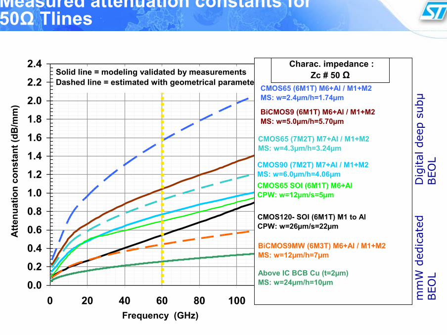
Measured attenuation constants for 50Ω Tlines
0.0
0.2
0.4
0.6
0.8
1.0
1.2
1.4
1.6
1.8
2.0
2.2
2.4
0 20 40 60 80 100 120 140 160 180
Solid line = modeling validated by measurementsDashed line = estimated with geometrical parameters
Above IC BCB Cu (t=2µm) MS: w=24µm/h=10µm
BiCMOS9 (6M1T) M6+Al / M1+M2MS: w=5.0µm/h=5.70µm
CMOS90 (7M2T) M7+Al / M1+M2MS: w=6.0µm/h=4.06µm
CMOS65 (7M2T) M7+Al / M1+M2MS: w=4.3µm/h=3.24µm
CMOS65 (6M1T) M6+Al / M1+M2MS: w=2.4µm/h=1.74µm
Frequency (GHz)
Atte
nuat
ion
cons
tant
(dB
/mm
)
CMOS120- SOI (6M1T) M1 to Al CPW: w=26µm/s=22µm
Charac. impedance : Zc # 50 Ω
BiCMOS9MW (6M3T) M6+Al / M1+M2 MS: w=12µm/h=7µm
CMOS65 SOI (6M1T) M6+Al CPW: w=12µm/s=5µm
mm
W d
edic
ated
BEO
LD
igital
dee
psu
bµ
BEO
L

HR SOI performances up to 100 GHz• Specific HR SOI CPW stacking all the metallizations
has been realized and characterised up to 110 GHz
• The obtained performances are: α ~ 0.5 dB/mm @ 50 GHz
InPSOI (stacked)SOI (top level)
Dimension of the stacked CPW line: w = 26 µm, s = 22 µm
CPW cross section Frequency (GHz) A
ttenu
atio
n (d
B)
40 80 100 20 0 60 0
0.2
0.4
0.6
1
0.8
Courtesy to F. Gianesello, STMicroelectronics

G band (140 – 200 GHz) CPW TL performances on SOI
attenuation in dB/mm and constant propagation
characteristic for a CPW transmission line realized on HR SOI with s = 10 µm and g = 5 µm
α ~ 1.5 dB/mm @ 200 GHz on HR SOI
Not feasible in bulk
Courtesy to F. Gianesello, STMicroelectronics

Outline
• Target applications for the Millimeter-wave frequency band
• Silicon technologies to address mmW complete solutions– Active devices on bulk and SOI technologies– Passive devices
• Silicon integrated solutions for mmW circuits– LNA mmW designs– Down-conversion mixers for mmW– Voltage controlled oscillators for mmW– Power amplifiers for mmW– mmW Assembly
•• ConclusionsConclusions
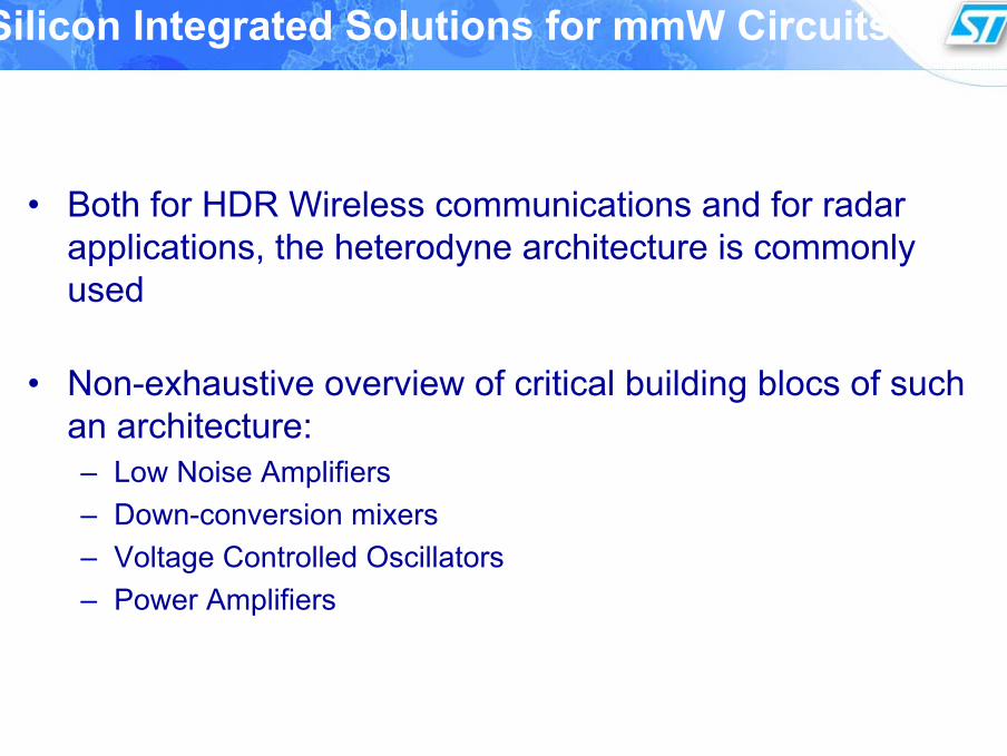
Silicon Integrated Solutions for mmW Circuits
• Both for HDR Wireless communications and for radar applications, the heterodyne architecture is commonly used
• Non-exhaustive overview of critical building blocs of such an architecture:– Low Noise Amplifiers– Down-conversion mixers– Voltage Controlled Oscillators– Power Amplifiers

Millimeter Wave Design Methodology
Generate a symbol for Agilent GoldenGate simulation
Results: S parametersADS dataset output formatPSF output format
Results: S parametersADS dataset output formatPSF output format
GUI
•Example: Agilent Momentum is used in the standard flow from virtuoso CADENCE environment
Courtesy to V. Poisson, Agilent Technolgiesand L. David, STMicroelectronics
mmW LNA Design Considerations
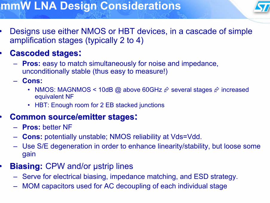
• Designs use either NMOS or HBT devices, in a cascade of simple amplification stages (typically 2 to 4)
•• CascodedCascoded stagesstages::– Pros: easy to match simultaneously for noise and impedance,
unconditionally stable (thus easy to measure!)– Cons:
• NMOS: MAGNMOS < 10dB @ above 60GHz several stages increased equivalent NF
• HBT: Enough room for 2 EB stacked junctions
•• Common source/emitter stagesCommon source/emitter stages::– Pros: better NF– Cons: potentially unstable; NMOS reliability at Vds=Vdd.– Use S/E degeneration in order to enhance linearity/stability, but loose some
gain
•• Biasing:Biasing: CPW and/or µstrip lines– Serve for electrical biasing, impedance matching, and ESD strategy.– MOM capacitors used for AC decoupling of each individual stage

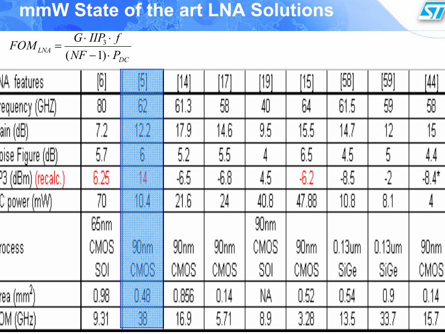
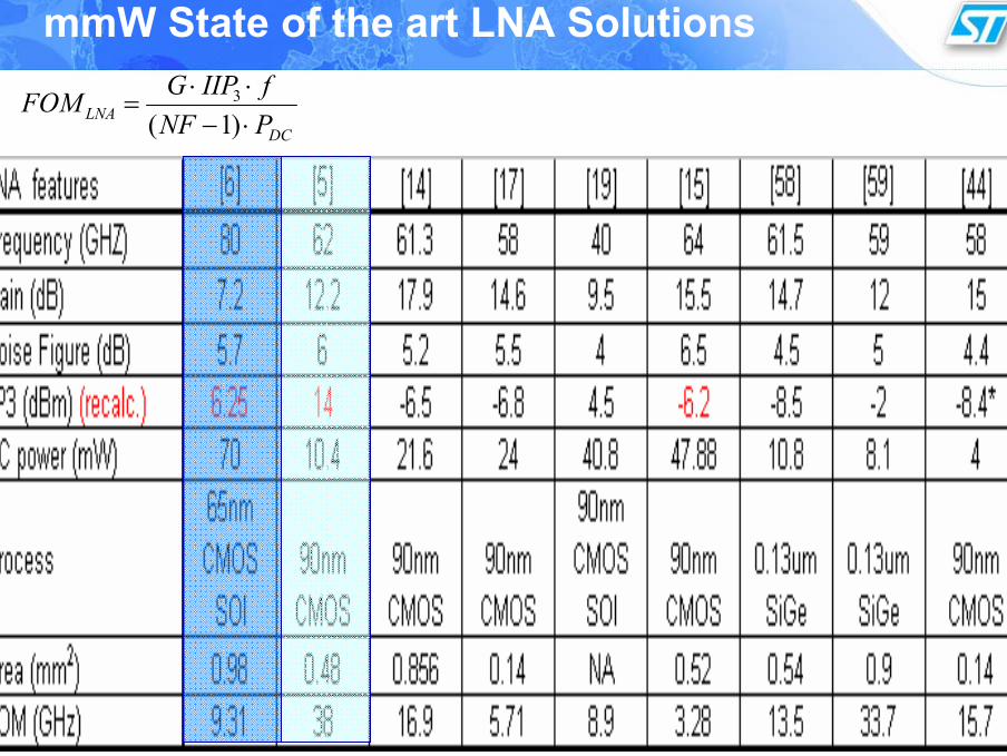
mmW State of the art LNA Solutions
DCLNA PNF
fIIPGFOM⋅−⋅⋅
=)1(3
mmW State of the art LNA Solutions
DCLNA PNF
fIIPGFOM⋅−⋅⋅
=)1(3
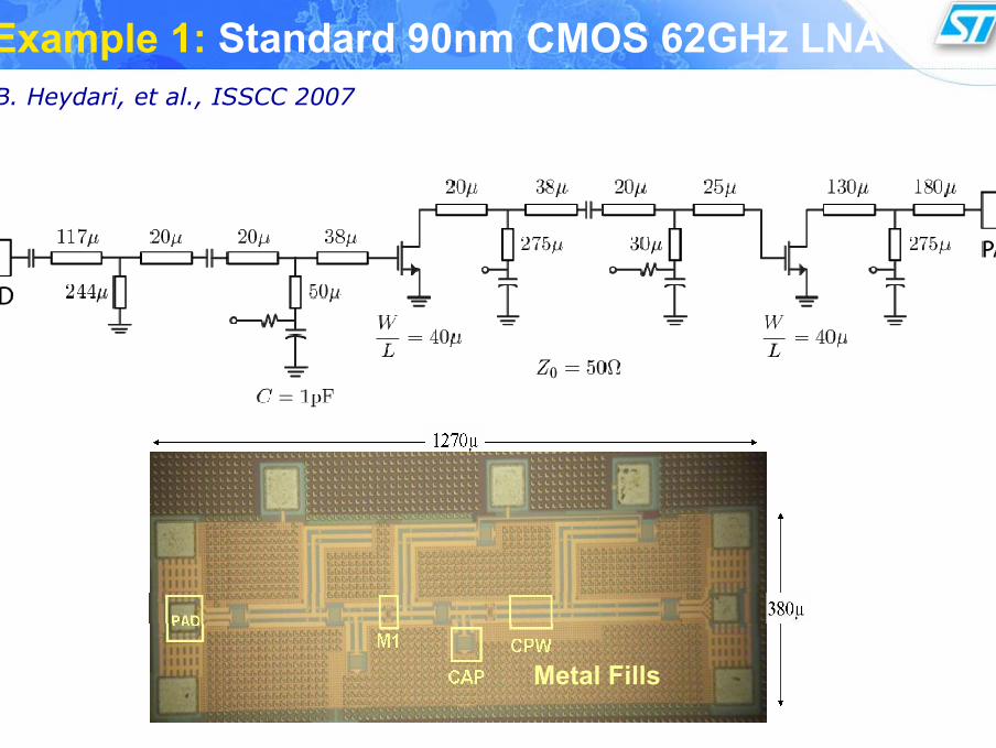
Example 1: Standard 90nm CMOS 62GHz LNA
Metal Fills
B. Heydari, et al., ISSCC 2007
mmW State of the art LNA Solutions
DCLNA PNF
fIIPGFOM⋅−⋅⋅
=)1(3

Example 2: 65nm LP SOI CMOS 80GHz LNAB. Martineau, et al., ESSCIRC 2007
Vg bias1Vdd=1V
RiRo
Ci
CPW LineZ0=70Ω
Co
mm-wavePAD OUT
mm-wavePAD IN
M1
1 pF
1 pF
1 pF1 pFM2 M3
RiRo
CiCo
RiRo
CiCo
Vg bias2 Vg bias3Vdd=1V Vdd=1V
CPW LineZ0=50Ω
IN OUT
Vg1 Vddgnd Vdd gndVg2 Vdd Vg3
Area = 0.98mm²(incl. pads)

mmW State of the art LNA Solutions
DCLNA PNF
fIIPGFOM⋅−⋅⋅
=)1(3
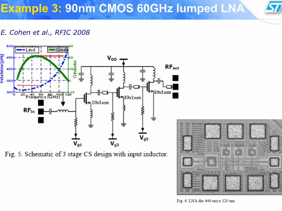
Example 3: 90nm CMOS 60GHz lumped LNA
E. Cohen et al., RFIC 2008

mmW State of the art LNA Solutions
DCLNA PNF
fIIPGFOM⋅−⋅⋅
=)1(3
FOM LNA
9.31
38
16.9
5.718.9
3.28
13.5
33.7
15.7
05
10152025303540
0 20 40 60 80 100
Frequency (GHz)
FOM
(GHz
)
FOM LNA
90nm CMOSSiGe HBT
SOI CMOS
The LNA design performances depends on the NFmin, (Ft) of the process and the Matching network:
mmW LNA is Designer dependent.CMOS and SiGe performances are similar.
mmW Down-conversion Mixers Design Considerations
•• Active mixers topologies:Active mixers topologies:– NMOS or HBT devices, Gilbert cells, Gm-cells, single or balanced inputs
for RF and LO– Pros: high conversion gain value, need for reduced LO power, good
noise figure– Cons: important power consumption, limited linearity, wide-band LO and
RF ports matching sometimes difficult to obtain
•• Passive (resistive) mixers topologies:Passive (resistive) mixers topologies:– NMOS transistor LO-pumped on the gate or on the source, RF applied
on the drain, the gate or combined with the LO on the gate– Pros: very linear large signal behavior, zero DC power consumption
(supports low supply voltage)– Cons: conversion losses, sometimes need for higher LO power w.r.t.
active mixers, LO to RF isolation sometimes low
•• For both categories:For both categories: sometimes sub-harmonic mixers (1/2, 1/3 LO signal)
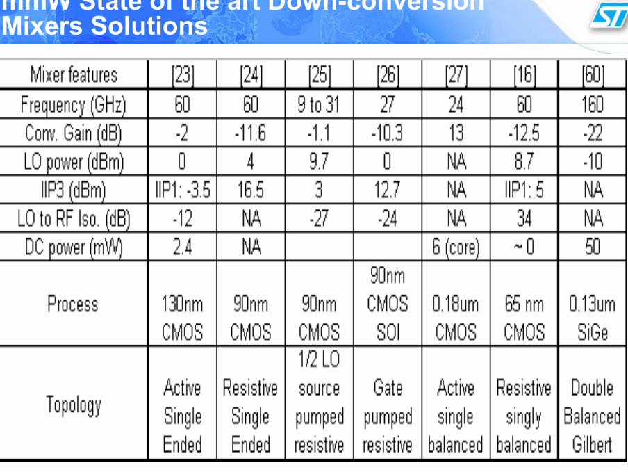
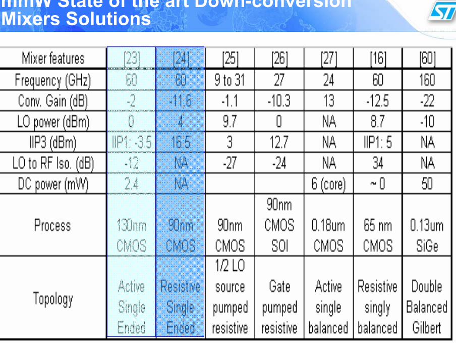
mmW State of the art Down-conversion Mixers Solutions
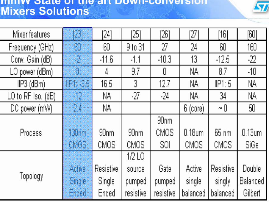
mmW State of the art Down-conversion Mixers Solutions
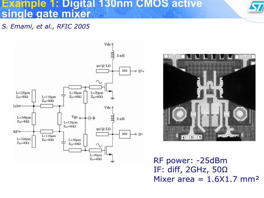
Example 1: Digital 130nm CMOS active single gate mixerS. Emami, et al., RFIC 2005
RF power: -25dBmIF: diff, 2GHz, 50ΩMixer area = 1.6X1.7 mm²
mmW State of the art Down-conversion Mixers Solutions

Example 2: Digital 90nm CMOS passive (resistive) gate-pumped mixerB.M. Motlagh, et al., IEEE M&W Comp. Letters, Jan. 2006
IIP3 + 3dB if Vds=150mV (power: 0.15mW)IF: 2GHz, 50ΩMixer area = 2X2 mm²

mmW State of the art Down-conversion Mixers Solutions
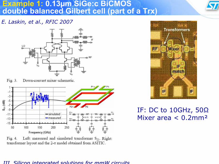
Example 1: 0.13µm SiGe:c BiCMOSdouble balanced Gilbert cell (part of a Trx)
III. Silicon integrated solutions for mmW circuitsIII. Silicon integrated solutions for mmW circuits
E. Laskin, et al., RFIC 2007
IF: DC to 10GHz, 50ΩMixer area < 0.2mm²
mmW State of the art Down-conversion Mixers Solutions
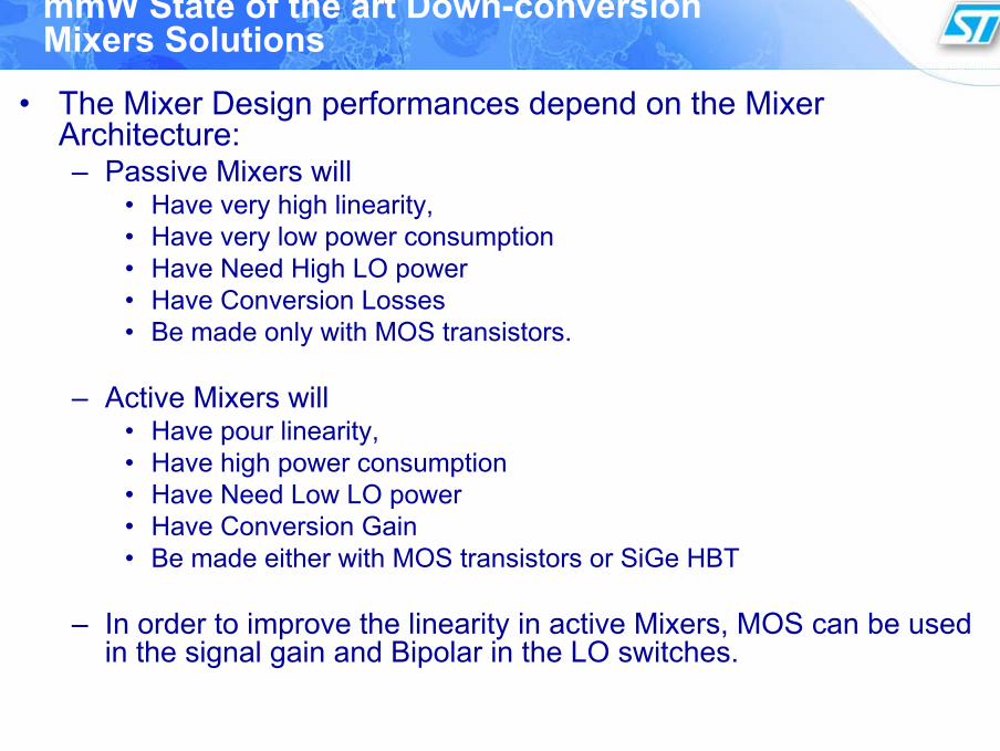
• The Mixer Design performances depend on the Mixer Architecture:– Passive Mixers will
• Have very high linearity, • Have very low power consumption • Have Need High LO power• Have Conversion Losses • Be made only with MOS transistors.
– Active Mixers will• Have pour linearity, • Have high power consumption • Have Need Low LO power• Have Conversion Gain• Be made either with MOS transistors or SiGe HBT
– In order to improve the linearity in active Mixers, MOS can be used in the signal gain and Bipolar in the LO switches.
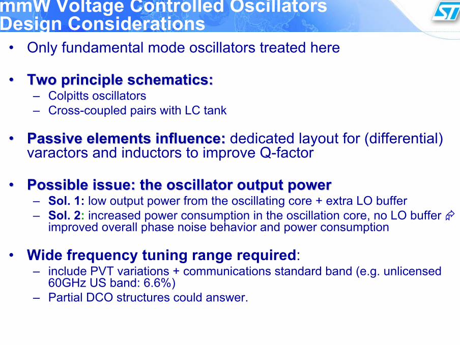
mmW Voltage Controlled Oscillators Design Considerations
• Only fundamental mode oscillators treated here
•• Two principle schematics:Two principle schematics:– Colpitts oscillators– Cross-coupled pairs with LC tank
•• Passive elements influence:Passive elements influence: dedicated layout for (differential) varactors and inductors to improve Q-factor
•• Possible issue: the oscillator output powerPossible issue: the oscillator output power– Sol. 1: low output power from the oscillating core + extra LO buffer– Sol. 2: increased power consumption in the oscillation core, no LO buffer
improved overall phase noise behavior and power consumption
• Wide frequency tuning range required: – include PVT variations + communications standard band (e.g. unlicensed
60GHz US band: 6.6%)– Partial DCO structures could answer.

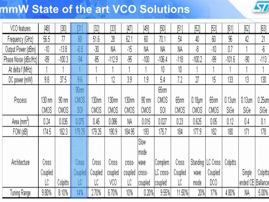
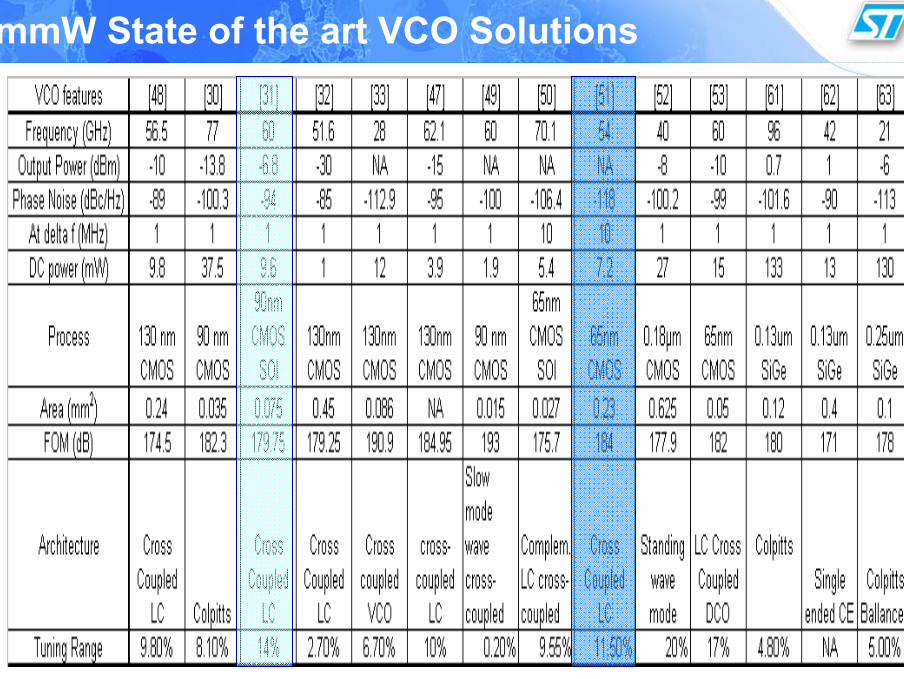
mmW State of the art VCO Solutions
PfLffFOMVCO ⋅
⋅
∆
=)(
12
0
mmW State of the art VCO Solutions

Example 1: 90nm SOI CMOS 60GHz cross-coupled LC VCOF. Ellinger, et al., IMS 2004
Area=0.3X0.25mm²Std resistivity substrate (15Ω.cm)Very large frequency tuning range by:-Large varactor size (thick oxyde MOS caps)-Small transistor size
mmW State of the art VCO Solutions
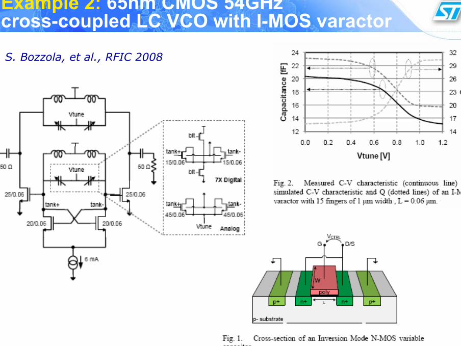
Example 2: 65nm CMOS 54GHz cross-coupled LC VCO with I-MOS varactor
S. Bozzola, et al., RFIC 2008
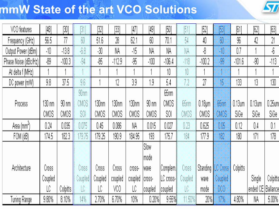
mmW State of the art VCO Solutions
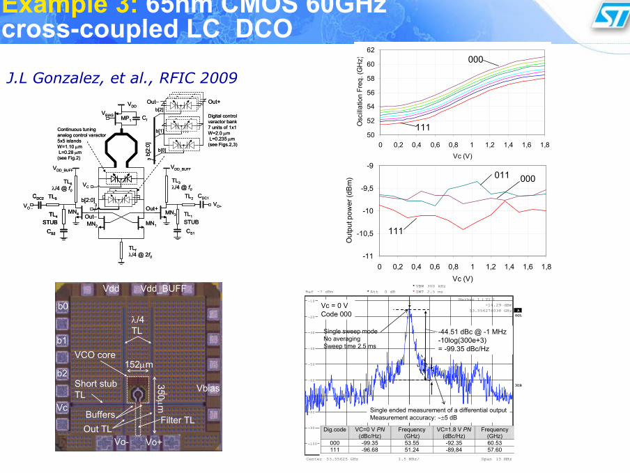
Example 3: 65nm CMOS 60GHz cross-coupled LC DCO
J.L Gonzalez, et al., RFIC 2009
VC
3b[2:0]
VBIAS
VO+VO − Out+Out−
CS1
TL1
STUB
TL2 CDC1
TL3λ/4 @ f0
VDD_BUFF
Cf
TLfλ/4 @ 2f0
VDD_BUFF
VDD
MN1MN2
MN3
CS2
TL4
STUB
TL5CDC2
TL6λ/4 @ f0
MN4
MP1
b[0]
Out+Out−b[2]
b[1]
3b[
2:0]
Digital controlvaractor bank7 units of 1x1W=2.0 µmL=0.235 µm(see Figs.2,3)
Continuous tuninganalog control varactor5x5 islandsW=1.10 µmL=0.28 µm
(see Fig.2)
VC
3b[2:0]
VBIAS
VO+VO − Out+Out−
CS1
TL1
STUB
TL2 CDC1
TL3λ/4 @ f0
VDD_BUFF
Cf
TLfλ/4 @ 2f0
VDD_BUFF
VDD
MN1MN2
MN3
CS2
TL4
STUB
TL5CDC2
CS2
TL4
STUB
TL5CDC2
TL6λ/4 @ f0
MN4
MP1
b[0]
Out+Out−b[2]
b[1]
33b[
2:0]
Digital controlvaractor bank7 units of 1x1W=2.0 µmL=0.235 µm(see Figs.2,3)
Continuous tuninganalog control varactor5x5 islandsW=1.10 µmL=0.28 µm
(see Fig.2)
VCO core
Vdd Vdd_BUFF
Vc
b2
b1
b0
Vbias
Vo- Vo+
Buffers
λ/4TL
Out TL
Short stubTL
Filter TL
152µm
350µm
VCO core
Vdd Vdd_BUFF
Vc
b2
b1
b0
Vbias
Vo- Vo+
Buffers
λ/4TL
Out TL
Short stubTL
Filter TL
152µm
350µm
Ref -7 dBm *
A
Att 0 dB *
1.5 MHz/Center 53.55625 GHz Span 15 MHz
**
3DB
RBW 300 kHz
VBW 300 kHz
SWT 2.5 ms*
SGL
-100
-90
-80
-70
-60
-50
-40
-30
-20
-10 1Marker 1 [T1 ]
-14.29 dBm
53.556274038 GHz
1
Delta 1 [T1 ]
-38.99 dB
1.009615385 MHz
Single ended measurement of a differential outputMeasurement accuracy: ∼±5 dB
Vc = 0 VCode 000
-44.51 dBc @ -1 MHz-10log(300e+3)= -99.35 dBc/Hz
Dig.code VC=0 V PN (dBc/Hz)
Frequency (GHz)
VC=1.8 V PN (dBc/Hz)
Frequency (GHz)
000 -99.35 53.55 -92.35 60.53 111 -96.68 51.24 -89,84 57.60
Single sweep modeNo averagingSweep time 2.5 ms
-11
-10,5
-10
-9,5
-9
0 0,2 0,4 0,6 0,8 1 1,2 1,4 1,6 1,8Vc (V)
Out
put p
ower
(dB
m)
50
52
54
56
58
60
62
0 0,2 0,4 0,6 0,8 1 1,2 1,4 1,6 1,8Vc (V)
Osc
illat
ion
Freq
. (G
Hz) 000
011
111
111
000
-11
-10,5
-10
-9,5
-9
0 0,2 0,4 0,6 0,8 1 1,2 1,4 1,6 1,8Vc (V)
Out
put p
ower
(dB
m)
50
52
54
56
58
60
62
0 0,2 0,4 0,6 0,8 1 1,2 1,4 1,6 1,8Vc (V)
Osc
illat
ion
Freq
. (G
Hz) 000
011
111
111
000
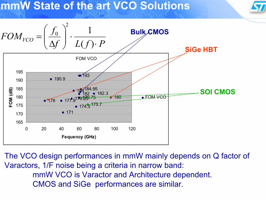
mmW State of the art VCO Solutions
PfLffFOMVCO ⋅
⋅
∆
=)(
12
0 Bulk CMOS
SOI CMOS
The VCO design performances in mmW mainly depends on Q factor ofVaractors, 1/F noise being a criteria in narrow band:
mmW VCO is Varactor and Architecture dependent.CMOS and SiGe performances are similar.
FOM VCO
174.5
182.3179.75179.25
190.9
184.95
193
175.7
184
177.9182
180
171
178
165
170
175
180
185
190
195
0 20 40 60 80 100 120
Fequency (GHz)
FOM
(dB
)
FOM VCO
SiGe HBT
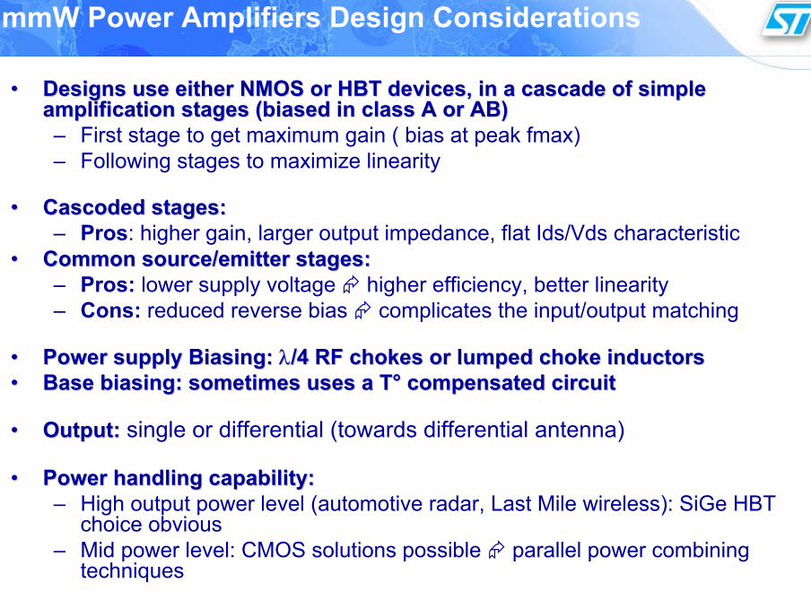
mmW Power Amplifiers Design Considerations
•• Designs use either NMOS or HBT devices, in a cascade of simple Designs use either NMOS or HBT devices, in a cascade of simple amplification stages (biased in class A or AB)amplification stages (biased in class A or AB)– First stage to get maximum gain ( bias at peak fmax)– Following stages to maximize linearity
•• CascodedCascoded stages:stages:– Pros: higher gain, larger output impedance, flat Ids/Vds characteristic
•• Common source/emitter stages:Common source/emitter stages:– Pros: lower supply voltage higher efficiency, better linearity– Cons: reduced reverse bias complicates the input/output matching
•• Power supply Biasing: Power supply Biasing: λλ/4 RF chokes or lumped choke inductors/4 RF chokes or lumped choke inductors•• Base biasing: sometimes uses a TBase biasing: sometimes uses a T°° compensated circuitcompensated circuit
•• Output:Output: single or differential (towards differential antenna)
•• Power handling capability:Power handling capability:– High output power level (automotive radar, Last Mile wireless): SiGe HBT
choice obvious– Mid power level: CMOS solutions possible parallel power combining
techniques
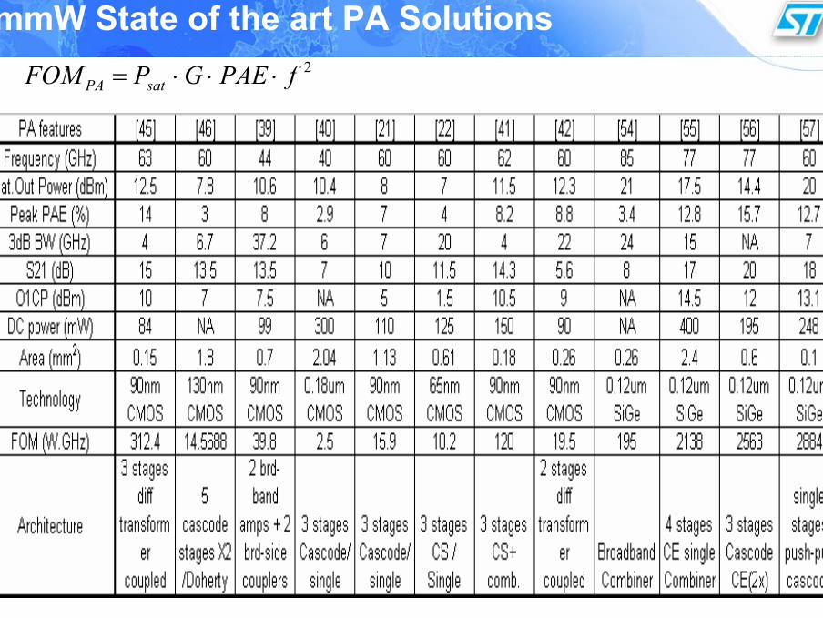
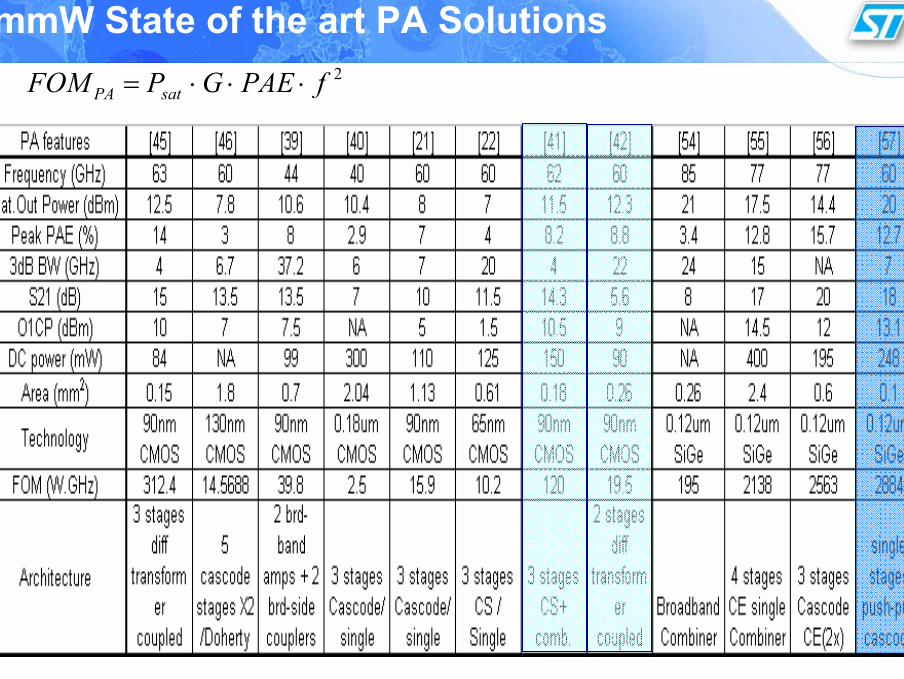
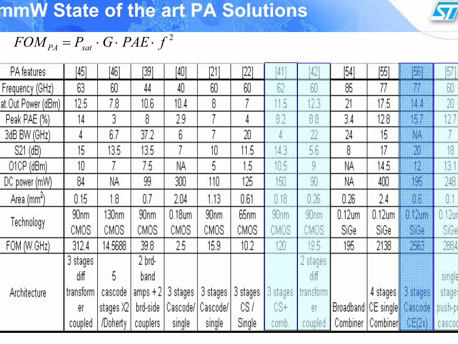
mmW State of the art PA Solutions 2fPAEGPFOM satPA ⋅⋅⋅=

mmW State of the art PA Solutions 2fPAEGPFOM satPA ⋅⋅⋅=
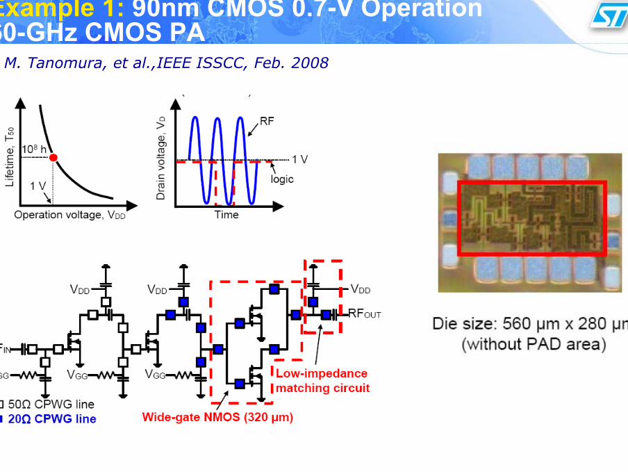
Example 1: 90nm CMOS 0.7-V Operation 60-GHz CMOS PA
M. Tanomura, et al.,IEEE ISSCC, Feb. 2008

mmW State of the art PA Solutions 2fPAEGPFOM satPA ⋅⋅⋅=
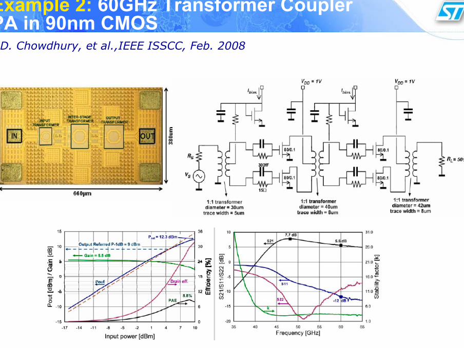
Example 2: 60GHz Transformer Coupler PA in 90nm CMOS
D. Chowdhury, et al.,IEEE ISSCC, Feb. 2008
mmW State of the art PA Solutions 2fPAEGPFOM satPA ⋅⋅⋅=
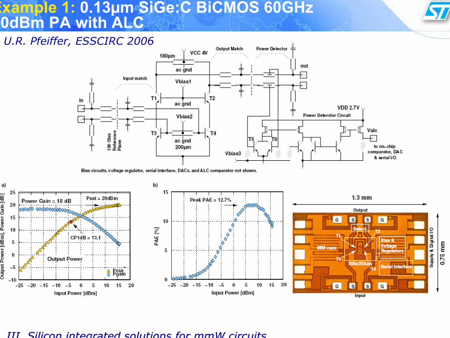
Example 1: 0.13µm SiGe:C BiCMOS 60GHz 20dBm PA with ALC
III. Silicon integrated solutions for mmW circuitsIII. Silicon integrated solutions for mmW circuits
U.R. Pfeiffer, ESSCIRC 2006
mmW State of the art PA Solutions 2fPAEGPFOM satPA ⋅⋅⋅=
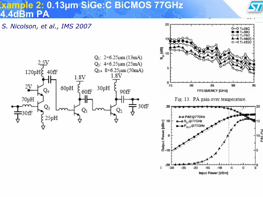
Example 2: 0.13µm SiGe:C BiCMOS 77GHz 14.4dBm PA
S. Nicolson, et al., IMS 2007
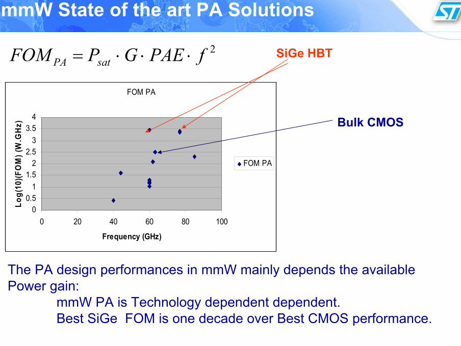
mmW State of the art PA Solutions
Bulk CMOS
The PA design performances in mmW mainly depends the available Power gain:
mmW PA is Technology dependent dependent.Best SiGe FOM is one decade over Best CMOS performance.
SiGe HBT 2fPAEGPFOM satPA ⋅⋅⋅=
FOM PA
00.5
11.5
22.5
33.5
4
0 20 40 60 80 100
Frequency (GHz)
Log(
10)(F
OM
) (W
.GH
z)
FOM PA

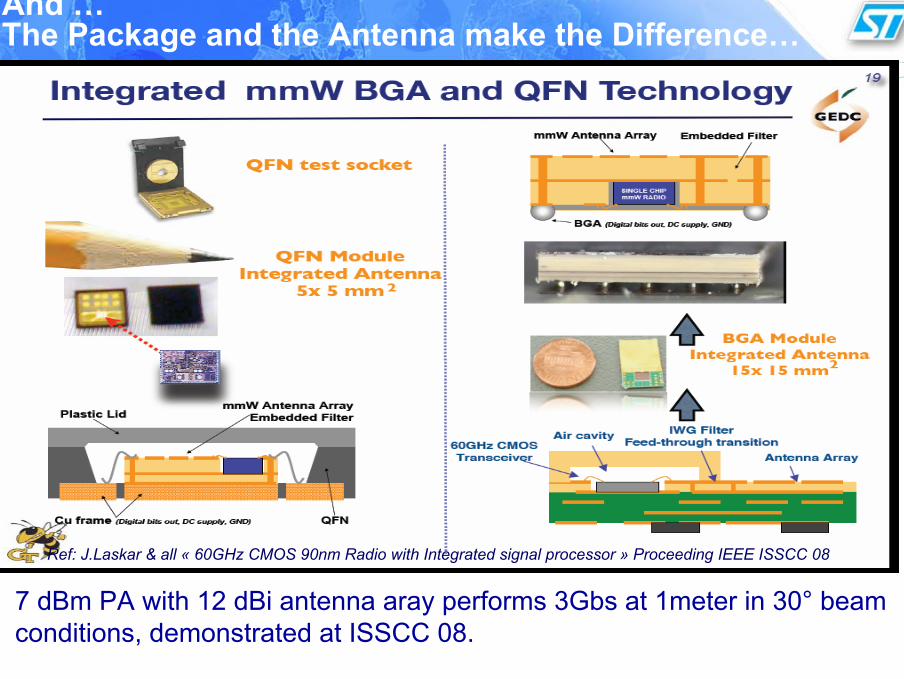
And …The Package and the Antenna make the Difference…
20 dBm PA with 7dBi antenna performs 700Mbs at 10meters in directiveconditions, demonstrated at ISSCC 06 by IBM.
And …The Package and the Antenna make the Difference…
7 dBm PA with 12 dBi antenna aray performs 3Gbs at 1meter in 30° beamconditions, demonstrated at ISSCC 08.
Ref: J.Laskar & all « 60GHz CMOS 90nm Radio with Integrated signal processor » Proceeding IEEE ISSCC 08
And …The Package and the Antenna make the Difference…
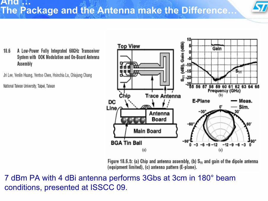
7 dBm PA with 4 dBi antenna performs 3Gbs at 3cm in 180° beamconditions, presented at ISSCC 09.
And …What About the coupling effects…
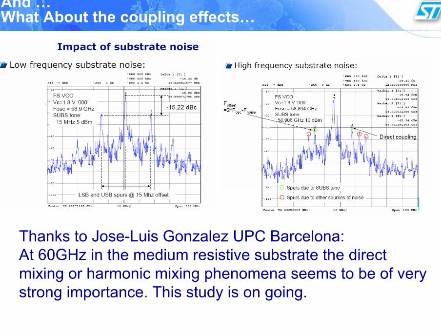
Thanks to Jose-Luis Gonzalez UPC Barcelona:At 60GHz in the medium resistive substrate the direct mixing or harmonic mixing phenomena seems to be of very strong importance. This study is on going.
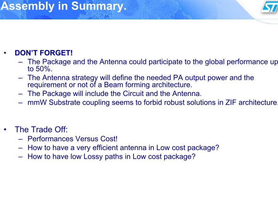
•• DONDON’’T FORGET!T FORGET!– The Package and the Antenna could participate to the global performance up
to 50%.– The Antenna strategy will define the needed PA output power and the
requirement or not of a Beam forming architecture.– The Package will include the Circuit and the Antenna.– mmW Substrate coupling seems to forbid robust solutions in ZIF architecture.
• The Trade Off:– Performances Versus Cost!– How to have a very efficient antenna in Low cost package?– How to have low Lossy paths in Low cost package?
Assembly in Summary.

Outline
• Target applications for the Millimeter-wave frequency band
• Silicon technologies to address mmW complete solutions– Active devices on bulk and SOI technologies– Passive devices
• Silicon integrated solutions for mmW circuits– LNA mmW designs– Down-conversion mixers for mmW– Voltage controlled oscillators for mmW– Power amplifiers for mmW– mmW Assembly
•• ConclusionsConclusions
Industrial Silicon mmW applications SWOT (I)
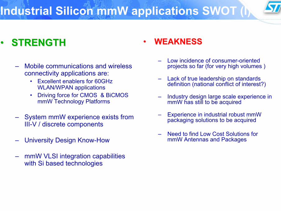
•• STRENGTHSTRENGTH
– Mobile communications and wireless connectivity applications are:
• Excellent enablers for 60GHz WLAN/WPAN applications
• Driving force for CMOS & BiCMOSmmW Technology Platforms
– System mmW experience exists from III-V / discrete components
– University Design Know-How
– mmW VLSI integration capabilities with Si based technologies
•• WEAKNESSWEAKNESS
– Low incidence of consumer-oriented projects so far (for very high volumes )
– Lack of true leadership on standards definition (national conflict of interest?)
– Industry design large scale experience in mmW has still to be acquired
– Experience in industrial robust mmW packaging solutions to be acquired
– Need to find Low Cost Solutions for mmW Antennas and Packages

•• OPPORTUNITIESOPPORTUNITIES
– Automotive applications, at mid-term, may become:
• Enablers for radar applications• Driving force for mmW BiCMOS
Technology Platforms
– Si technology mmW capability is a « More than Moore » feature which opens opportunities for leadership in specific areas
– mmW-oriented VLSI CAD Design Platforms availability to come
– Emerging applications for THz integrated devices:
• Imaging for Medical and Safety /Security Applications
• 100Gb/s Ethernet Fiber Optics communications
•• THREATSTHREATS
– Economic crisis may delay mmW consumer applications ramp-up
– Competition between geographical areas for standard supremacy
– Use of leading edge 300mm fabs requires several Billions € market in CMOS approach
– BiCMOS offer is limited to few foundries which limit second sources possibilities.
Industrial Silicon mmW applications SWOT (II)
Acknowledgements
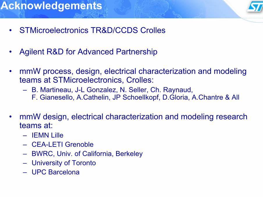
• STMicroelectronics TR&D/CCDS Crolles
• Agilent R&D for Advanced Partnership
• mmW process, design, electrical characterization and modeling teams at STMicroelectronics, Crolles:– B. Martineau, J-L Gonzalez, N. Seller, Ch. Raynaud,
F. Gianesello, A.Cathelin, JP Schoellkopf, D.Gloria, A.Chantre & All
• mmW design, electrical characterization and modeling research teams at:– IEMN Lille– CEA-LETI Grenoble– BWRC, Univ. of California, Berkeley– University of Toronto– UPC Barcelona
References (I)1. B. Floyd, et al., “Silicon Tehcnology, Circuits, Packages, and Systems for 60-100
GHz”, RFIC 2007 WSN Workshop: “Millimeter-wave/Quasi – Millimeter-Wave Highly-Integrated Circuits”, Honolulu, June 2007
2. C.S.Park, “ SoP Integration of 60GHz Radio”, RFIC 2007 WSN Workshop: “Millimeter-wave/Quasi – Millimeter-Wave Highly-Integrated Circuits”, Honolulu, June 2007
3. P. Chevalier, “STMicroelectronics Foundry Services for mmW Frequencies”, ESSCIRC2006 Wireless Communications Workshop: “1Gbit/s+ wireless communications at 60GHz and beyond”, Montreux, Sept. 2006
4. P. Chevalier, et al., “Advanced SiGe BiCMOS and CMOS platforms for Optical and Millimeter-Wave Integrated Circuits”, IEEE CSICS 2006
5. B. Heydari, et al., “Low Power mm-Wave Components up to 104 GHz in 90nm CMOS”, ISSCC2007, San Francisco, Feb. 2007
6. B. Martineau, et al., “80 GHz Low Noise Amplifiers in 65nm CMOS SOI”, ESSCIRC2007, Munich, Sept. 2007
7. C. Raynaud et al.,”Is SOI CMOS a promising Technology for SOCs in High Frequency range?“, in Proc. 207th ECS, 2005, pp. 331-344.
8. T.O. Dickson, et al., ”The Invariance of Characteristic Current Densities in Nanoscale MOSFETs and Its Impact on Algorithmic Design Methodologies and Design Porting of Si(Ge) (Bi)CMOS High-Speed Building Blocks“, IEEE JSSC, vol. 41, No. 8, Aug. 2006
9. P. Chevalier, et al., “High-Speed SiGe BiCMOS Technologies: 120-nm Status and End-of-Roadmap Challenges”, 7th Topical Meeting on Silicon Monolithic Integrated Circuits in RF Systems (SiRF07), Long Beach, Jan. 2007
10.F. Gianesello, et al., “65nm HR SOI CMOS Technology: emergence of Millimeter-Wave SoC”, RFIC2007, Honolulu, June 2007

References (II)
11. N. Seller, et al., “A 10GHz Distributed Voltage Controlled Oscillator for WLAN Application in a VLSI 65nm CMOS Process”, RFIC2007, Honolulu, June 2007
12. http://eesof.tm.agilent.com/products/momentum_main.html13. http://www.ansoft.com/products/hf/hfss/14. M.A.T. Sanduleanu, “60 GHz Integrated Circuits and Wireless Systems”,
ESSCIRC2006 Wireless Communications Workshop: “1Gbit/s+ wireless communications at 60GHz and beyond”, Montreux, Sept. 2006
15. S.Pellerano et al., “A 64GHz 6.5dB NF 15.5dB Gain LNA in 90nm CMOS”, IEEE ESSCIRC2007, Munich, September 2007
16. Mikko Varonen et al,“V-band Balanced Resistive Mixer in 65-nm CMOS”IEEE ESSCIRC2007, Munich, September 2007
17. T. Yao, et al., “Algorithmic Design of CMOS LNAs and Pas for 60-GHz Radio”, IEEE Journal of Solid-State Circuits, Vol. 42, No. 5, May 2007
18. Ch. Weyers, et al., “A 22.3dB Voltage Gain 6.1dB NF 60GHz LNA in 65nm CMOS with Differential Output ”, IEEE ISSCC, San Francisco, February2008
19. F. Ellinger, ”26-42 GHz SOI CMOS low noise amplifier,” JSSC, March 2004, Pages: 522- 528
20. E. Laskin, et al., ”80/160-GHz Transceiver and 140-GHz Amplifier in SiGe Technology ”, RFIC2007, Honolulu, June 2007

References (III)21. M.A.T. Sanduleanu et al., “A Millimeter-Wave Power Amplifier with 25dB
Power Gain and +8dBm Saturated Output Power”, IEEE ESSCIRC2007, Munich, September 2007
22. M.Varonen, et al., “Millimeter-Wave Amplifiers in 65-nm CMOS”, IEEE ESSCIRC2007, Munich, September 2007
23. S. Emami, et al., “A 60-Ghz Down-Converting CMOS Single-Gate Mixer”, RFIC2005, Long Beach, 2005
24. B.M. Motlagh, et al., “Fully Integrated 60-GHz Single-Ended Resistive Mixer in 90-nm CMOS Technology”, IEEE Microwave and Wireless Components Letters, Vol.16, No. 1, Jan. 2006
25. M. Bao, et al., “A 9-31 GHz Subharmonic Passive Mixer in 90-nm CMOS Technology”, IEEE Journal of Solid State Circuits, Vol. 41, No. 10, Oct. 2006
26. F. Ellinger, “26.5-30-GHz Resistive Mixer in 90-nm VLSI SOI CMOS Technology with High Linearity for WLAN”, IEEE Transactions on Microwave Theory and Tehcniques, Vol. 53, No. 8, Aug. 2005
27. X. Guan et al., “A 24-GHz CMOS Front-End”, IEEE Journal of Solid State Circuits, Vol. 39, No. 2, Feb. 2004
28. C. Cao, et al., “CMOS Millimeter-Wave Frequency Sources”, RFIC 2007 WSN Workshop: “Millimeter-wave/Quasi – Millimeter-Wave Highly-Integrated Circuits”, Honolulu, June 2007
29. S.T. Nicolson, et al, “ Design and Scaling of SiGe BiCMOS VCOs Above 100GHz”, IEEE BCTM 2006
30. K.W. Tang, et al, “ Frequency Scaling and Topology Comparison of Millimeter-wave CMOS VCOs”, IEEE CSICS 2006
References (IV)
31.F. Ellinger, et al, “60GHz VCO with Wideband Tuning Range Fabricated on VLSI SOI CMOS Technology”, 2004 IEEE MTT-S Digest, IMS 2004
32.M. Tiebout, et al., “ A 1V 51GHz Fully-Integrated VCO in 0.12µm CMOS”, IEEE ISSCC 2002, San Francisco, Feb. 2002
33.Y. Wachi, et al., “A 28GHz Low-Phase-Noise CMOS VCO Using an Amplitude-Redistribution Technique”, IEEE ISSCC 2008, San Francisco, Feb 2008
34.E. Afshari, et al, “Electrical funnel: A broadband signal combining method,”IEEE International Solid-State Circuits Conference, pp. 206–207, Feb. 2006.
35.A. Komijani, et al, “A Wideband 77-GHz, 17.5-dBm Fully Integrated Power Amplifier in Silicon”, IEEE Journal of Solid State Circuits, Vol. 41, No. 8, Aug. 2006
36.S.T. Nicolson, et al, “ A Low-Voltage 77-GHz Automotive Radar Chipset”, 2007 IEEE MTT-S Digest, IMS 2007
37.Ullrich R. Pfeiffer, “A 20dBm Fully-Integrated 60GHz SiGe Power Amplifier with Automatic Level Control”, IEEE 2006 ESSCIRC, Montreux, Sept. 2006
38.C.H. Doan, “Millimeter-Wave CMOS Design”, IEEE Journal of Solid State Circuits, Vol. 40, No. 1, Jan. 2005
39.J-H Tsai, et al., ” A 90-nm CMOS Broadband and Miniature Q-band Balanced Medium Power Amplifier”, RFIC2007, Honolulu, June 2007
40.H. Shigematsu, et al., “Millimeterwave CMOS circuit design,” IEEE Trans. Microw. Theory Tech., vol. 53, no. 2, pp.472-477, Feb. 2005.
References (V)
41. M. Tanomura, et al., “TX and RX Front-Ends for 60GHz Band in 90nm Standard Bulk CMOS”, IEEE ISSCC 2008, San Francisco, Feb 2008
42. D. Chowdhury, et al., “ A 60GHz 1V +12.3dBm Transformer-Coupled WidebandPA in 90nm CMOS ”, IEEE ISSCC 2008, San Francisco, Feb 2008
43. T. Suzuki, et al., “ 60 and 77GHz Power Amplifiers in Standard 90nm CMOS”, IEEE ISSCC 2008, San Francisco, Feb 2008
44. E. Cohen, et al., “An ultra low power LNA with 15dB gain and 4.4dB NF in 90nm CMOS process for 60GHz phase array radio ”, IEEE RFIC 2008, Atlanta, June2008
45. T. LaRocca, et al., “60GHz CMOS Differential and Transformer-Coupled Power Amplifier for Compact Design ”, IEEE RFIC 2008, Atlanta, June 2008
46. B. Wicks, et al., “A 60GHz Fully-Integrated Doherty Power Amplifier Based on 0.13µm CMOS Process”, IEEE RFIC 2008, Atlanta, June 2008
47. J. Borremans et al., “VCO design for 60Ghz applications using differentialshielded inductors in 0.13µm CMOS”, IEEE RFIC 2008, Atlanta, June 2008
48. C. Cao and K. K. O, “Millimeter-wave voltage-controlled oscillators in 0.13-mm technology,” IEEE J. Solid-State Circuits, vol. 41, no. 6, pp. 1297–1304, Jun. 2006.
49. D. Huang, W. Hant, N.-Y.Wang, T. W. Ku, Q. Gu, R.Wong, and M.-C. F. Chang, “A 60 GHz CMOS VCO using on-chip resonator with embedded artificialdielectric for size, loss and noise reduction,” in IEEE Int. Solid-State Circuits Conf. (ISSCC) Dig. Tech. Papers, 2006, pp. 314–315

References (VI)50. D. D. Kim, J. Kim, J. Plouchart, C. Cho, W. Li, D. Lim, R. Trzcinski, M. Kumar, C. Norris and D.
Ahlgren, “A 70GHz Manufacturable Complementary LC-VCO with 6.14GHz Tuning Range in 65nm SOI CMOS”, IEEE ISSCC Dig. Tech. Papers, pp. 540-541, February 2007.
51. S. Bozzola, D. Guermandi, A. Manzzanti, F. Svelto, “An 11.5% frequency tuning, -184 dBc/Hz noise FOM 54 GHz VCO, IEEE Radio Frequency Integrated Circuits Symposimum (RFIC), 2008, pp. 657-660.
52. J-C Chien and L-H Lu, “Design of Wide-Tuning-Range Millimeter Wave CMOS VCO With a Standing-Wave Architecture”, IEEE Journal of Solid-State Circuits, vol. 42, no 9, pp. 1942-1952, September 2007.
53. José Luis González Jiménez et al. “A 56GHz LC-Tank VCO with 17% Tuning Range in 65nm Bulk CMOS for Wireless HDMI Applications” RFIC2009, Boston, June 09
54. E. Afshari, et al, “Electrical funnel: A broadband signal combining method,” IEEE International Solid-State Circuits Conference, pp. 206–207, Feb. 2006
55. A. Komijani, et al, “A Wideband 77-GHz, 17.5-dBm Fully Integrated Power Amplifier in Silicon”, IEEE Journal of Solid State Circuits, Vol. 41, No. 8, Aug. 2006
56. S.T. Nicolson, et al, “ A Low-Voltage 77-GHz Automotive Radar Chipset”, 2007 IEEE MTT-S Digest, IMS 2007
57. Ullrich R. Pfeiffer, “A 20dBm Fully-Integrated 60GHz SiGe Power Amplifier with Automatic Level Control”, IEEE 2006 ESSCIRC, Montreux, Sept. 2006
58. B. Floyd et al., “SiGe Bipolar Transceiver Circuits Operating at 60GHz ,” IEEE Journal of Solid-State Circuits, pp. 156-167, Jan. 2005
59. J. Alvarado, et al., “60-GHz LNA using a Hybrid Transmission Line and Conductive Path to Ground Technique in Silicon”, RFIC2007, Honolulu, June 2007
60. E. Laskin, et al., ”80/160-GHz Transceiver and 140-GHz Amplifier in SiGe Technology ”, RFIC2007, Honolulu, June 2007
61. S.T. Nicolson, et al, “ Design and Scaling of SiGe BiCMOS VCOs Above 100GHz”, IEEE BCTM 2006
62. S. Pruvost, et al., “A 40GHz Superheterodyne Receiver Integrated in 0.13µm BiCMOS SiGe:C HBT Technology“, BCTM 2005
63. M. Bao, et al., “A 21.5/43 GHz Dual-Frequency Balanced Colpitts VCO in SiGe Technology”, IEEE Journal of Solid State Circuits, Vol. 39, No. 8, Aug. 2004