Embed Size (px)
Citation preview
1
Manual revision 1.5 C
M M S Electronics Ltd South View Business Park
Ghyll Royd – Guiseley - Leeds LS20 9LT England Tel UK (0)1943 877668 Email sales @ MMS-e.co.uk
MMS-C310 Series User’s Manual

2
Universal controller MMS-C310
Table of contents
Introduction ............................................................. 3 Input connection ...................................................... 4 Output connection ................................................... 5 Power supply selection ............................................. 6 Installation ............................................................... 7 Programming the MMS-C310 .................................. 11 Memory mapping ..................................................... 12 Description of the 80C552 I/O ports .........................13 Description of the control board connectors...............15 8051 ASM program examples .................................. 17 RS232 communications ............................................ 20 I2C communications ................................................ 20 Circuit drawing ........................................................ 21
This manual has been written for the reader who is familiar with digital logic and microprocessors. A specific knowledge of the 8051 processor family is not assumed, but it would be advisable for anyone not familiar with these microprocessors to obtain and read the ‘Single-chip 8 bit micro-controllers PCB83C552/562’ from Philips. or the handbook ‘Programming and interfacing the 8051 micro-controller’ from Addison-Wesley publishing company. M.M.S. Electronics technical and programming support is just one phone call away, we’re here to help you be more productive.

3
This universal mini controller is a compact, high performance true single board controller. It is perfectly suited for machine and process control. Low voltage valves, solenoids, motor drivers and input switches or sensors can be directly connected to the robust and removable I/O screw terminals. Features include:
- Fully opto isolated input outputs. - Heavy duty 2.5 mm circuit board with stand-offs. - Industrial removable input output connectors. - 16 inputs and 4 external interrupts. - Up to 7 relay outputs. - 39 transistor outputs. - Buffered keypad connector for up to 16 buttons. (4*4 matrix) - LCD connector for MMS-T105 terminal or other dot matrix LCD’s. - RS232 serial port without the need for ± 12 volt power supply. - I2C connectors for PC communication or expansion boards. - 3 digitally controlled potentiometer outputs (max. 1 mA) - 5 Analogue inputs to AD converter. - 2 Pulse modulated outputs ideal for motor control. - 2 on boards status LED’s - Real time calendar / clock. (optional) - Non-volatile memory with internal backup battery (+10 years). - Watch dog. - Fast instruction time 0.75 micro seconds with the 80C552 processor. - Program compilers widely for the 8051 processor available in ASM or C. - Full software support from M.M.S Electronics Ltd www.mms-e.com
Applications: Existing applications are in use all over the world for standard machine controls and machine controls with servo and stepper motor drives. Replacement for commercial PLC systems to allow for bespoke program control and easy operator interface. Examples are: Indexing systems with servo & stepper motor control. Automatic sewing machines, Pocket welt machine. Automatic stackers, production batch controller. Cut to length measuring device with encoder input.
Introduction to the MMS-C310

4
External Internal
All digital I/O on the input and output connectors are optically isolated. For maximum electrical noise immunity, power for the isolation must come from a power supply different then the one supplying the logic circuit. Inputs Input 50 to 69 : 20 standard inputs available on the control card. Input 66 to 69 : 4 Fast interrupts inputs Vmin 9V (default) Input ON voltage (1k) 6.5V (min) 30 Volt (max.) Input ON current 1.3 mA @ 6.5V 6.3 mA @ 12V 18.3mA @ 24V Input 66 to 69 : 4 fast interrupts inputs Input ON voltage (1k) 9.0V (min) 30 Volt (max.) Inputs are normally off when left open. Input sensors should be PNP type. Input 67 and 68 can also take the input from T1 and T2 for an incremental encoder. Internal diagram The following diagram shows the internal structure of a typical input on the input connector (pins 50 to pin 69).
CONNECTING Inputs
Input pin 50 - 69
1000 ohm
Zener 5.1V
P Gnd
OPTO

5
Outputs Output 1 to 3 . 3 relay outputs max. 5 Amp. (These outputs are available to use but relays fitted optional) Output 4 to 7 4 relay outputs max. 1A @ 24Vdc. (These relays are fitted as standard) Output 8 to 23, 25 to 32, 34 to 41. 32 transistor outputs drivers. Maximum output voltage 50V and max. output current per output is 500 mAmp (600 mAmp peak). The outputs are suitable for use with inductive loads like solenoids, relays and lamps. These outputs are fitted with transient protection diodes. The diodes are connected to pin 24 (out 8..23), 33 (out 25..32) and 42 (out 34..41). Internal diagram The following diagram shows the internal structure of a typical transistor output. Internal External
CONNECTING Outputs
+
Output pins 8 to 23 25 to 32 34 to 41
LOA
Diode protection Pin 24, 33, 42

6
For maximum electrical noise immunity, power to the controller needs to come from two power supply’s or a split voltage power supply or a filtered and isolated DC-DC converter. A good quality 5 Volt is needed to power the microprocessor and LCD circuit. The second voltage powers the transistors and the optical isolation to the board, this voltage is recommended 12, 15 or 24 Volt. (Max. 30 volt). If a switch mode power supply is chosen for the 5 volt supply then check that the minimum regulating current is below the small power consumption of the board ( Typical 150-200mAmp) . If this is not the case then a dummy load (resistor) may have to be put across the 5 Volt output terminals to increase the minimum current or alternatively select a linear power supply. Power supply connection Power 12 .. 24 Volt + - POWER P 24 V P GND P L Power supply 5 volt. GND 2 - + 5 V +
POWERSUPPLY SELECTION

7
When operating the MMS control card in a “noise polluted” industrial environment, special considerations should be given to eliminate possible electrical interference. Poor wiring standards may contribute to processor faults and sporadic operations. These problems tend not to show up until the system is installed and operating in its intended environment. For this reason extra care should be taken when wiring the equipment. Also it is the responsibility of the manufacturer if equipment is sold in the European market that these ‘be so constructed that they do not cause excessive electromagnetic interference and are not unduly affected by electromagnetic interference’. The MMS control card has been designed to give maximum protection against electrical interference by optically isolating the logic processor circuit from the potential noisy input/output circuit. This requires the need for two separate power supply’s or one power supply with a separated ground return for the 5 volt logic circuit and the higher voltage (12 or 24 volt) for the input output circuit. Other additional measures should be taken to reduce the effect of electrical interference.
a. Proper mounting of the controller within an enclosure. b. Proper routing of the wiring. c. Proper equipment grounding. d. Proper suppression added to noise generating devices.
a. Mounting of the controller within an enclosure. Position the control card in the enclosure so that the terminal connectors can be removed without having to remove the control card from the enclosure. Position the control card a minimum distance of 2 inches away from any AC source. Metal enclosures are very effective in preventing interference from external noisy sources such as motors and electrical brake ... b. Routing of the wiring. When connecting to the removable terminals leave enough slack in the wires so that the connectors can be removed when the control board is replaced without need to rewire. Every effort should be made to route signal leads away from ac sources of magnetic fields. Such sources include mains power, motors, transformers, relays coils or any leads wired to these devices. A relay coil being switched, a switch turning on a motor or switching on and off an electric typewriter can easily generate a transient potential difference (EMF) in excess of 1000 volts onto the AC powerlines. This voltage can easily couple into a nearby wire and cause severe problems.
INSTALLATION

8
M.M.S. CONTROL CARD Minimum distance that any AC source or motor Lcd harness cable should be routed away from controls. + 2 inch I/O Logic 5V power power supply. supply Filter AC mains filter may be needed Mains AC power lines to reduce incoming noise. If interference occurs and can not be avoided by moving the noisy equipment or rerouting the wires then shielded and/or twisted pair wire should be used. An effective method of reducing magnetic pick-up is using a pair of conductors with 30 to 50 twist per metre. The shield protects against capacitive coupled interference. When shielded cable is used never leave the shield unconnected or the shield may start acting as an aerial and introduce noise. If cables leaving the electrical enclosure have a very low amplitude or contain data above 10 kHz then shielding will be inevitable. Most of the times it should be sufficient to connect the shield end to ground on the cable side nearest to the control card. If the possible noise source is known then wire the shield end nearest to the noise source to ground. If unsure connect both shield ends to a common ground. (do read the ’ground loop’ information following. ) c. Equipment grounding.

9
By law all AC powered systems need to be earth-grounded. If a load circuit has a metal enclosure and one of the life wires develops a short to the enclosure then there will be a shock hazard to operating personnel, unless the enclosure itself is earth grounded. If the enclosure is earth grounded, a short results in a blown fuse rather than a “hot” enclosure. The idea is to run series connections for circuits that have similar noise properties, and connect then at a single reference point. Noisy signal ground connect to things like motors and relays. Hardware ground is the safety ground connection to the chassis, rack and cabinets. It’s a mistake to use hardware ground as a return path for signal currents because it’s fairly noisy and tends to have high resistance due to joints and seams. Screws and bolts don’t always make a good electrical connection because of galvanic action, corrosion, dirt and paint. These kinds of connections may work well at first, and then cause mysterious maladies as the system ages. In places where the machine hinges use a ground wire to link the two parts. quiet signal ground Noisy and high Hardware ground (encoder and terminal shield ) current signal ground (motor ground) Reference point. Incoming ground wire It is important to use one common ground point to connect the safety ground and the cable shielding to. The problem is that true earth ground is not really at the same potential in all locations. If two ends of a wire are earth grounded at different locations, the voltage difference between the two “ground” points can drive significant currents (several amperes) through the wire. This is the classic “ground loop” Consider this ground wire to be the shielding of the encoder harness and the protective shielding will often unexpectedly corrupt the data signals. d. Suppression added to noise generating devices. Potential noise generators include inductive loads, such as relays, solenoids, and motor starters when operated by push buttons or selector switches. Suppression may be necessary when such loads are connected as output devices or when connected to the same supply line that powers the controller. We recommend that the suppression device is located as close as possible to the load device The suppression will also add significant lifetime to the switch or relay contacts.

10
Common protection methods: Load Surge RC network across contacts suppresser. solenoid valve - + Diode 1N4004 is acceptable in most applications.
Programming the MMS-C310

11
MMS-e can fully develop the controller program for you, support your development engineers with advice or just supply you with the components. The following sheets document information to program the controller. Familiarity with the 8051 processor is recommended. To start programming you will need a standard IBM-PC with 8051 compiler software and an EPROM programmer. It is also possible with the Boot EPROM installed and serial port to download program code direct to the controller memory. No need for an EPROM programmer. Many 8051 assembler programs are available for download from the www. ( see www.atmel.com 8051 download section) or to program in ‘c’ use the Keil C-compiler. If you have any special requirements or questions on system implementation then do contact MMS-e.

12
The 80C552 processor internal data memory is divided in 3 sections: the lower 128 bytes of RAM, the upper 128 bytes of RAM and the special function registers. The lower 128 bytes of RAM are directly and indirectly addressable. The 80c552 contains six 8 bit I/O ports, three 16 bit timer / counters, a fifteen-source nested interrupt structure, an 8 bit input A to D converter, a dual pulse with modulated interface, two serial interfaces (UART and I2C bus), and a ‘watchdog’ timer. The external memory configuration is as follows: To allow correct timing of the serial port the board is fitted with a 14.74560 Mhz crystal. This will give exact baud rate timing. Otherwise the control board can be fitted with faster crystals. For very fast applications a 24Mhz processor version is available from Philips. When selecting different memory devices the access time has to be 150 nano seconds or less.
Memory mapping.
Description of the 80c552 i/o ports
Address 0000 - 3FFF 4000 - 5FFF 6000 - 6003 8000- FFFF
Description 16k-program memory Ic2 suitable for 27128 EPROM. (BOOT) 8k program or data memory. Socket Ic3 is supplied with 8k of non -volatile RAM (Dallas DS1225) or could also be fitted with DS1243 8k non-volatile RAM including a real-time clock and calendar. IO port 8255 responsible for controlling inputs 50 to 65 and outputs 25 to 41. Address 6000 is output byte for port 34 to 41. Address 6002 is output port 25 to 32. Address 6001 is the input matrix. Address 6003 is the port control register for the 8255. 32k program or non-volatile data memory. Socket Ic4 can be fitted with a 32k STK15C88. (Jedex approved pinout for byte wide memories)

13
Port Ic1 Pin no Description P0.0 57 AD0 Low order address and data bus (access external memory) P0.1 56 AD1 “ “ ” P0.2 55 AD2 “ “ “ P0.3 54 AD3 “ “ “ P0.4 53 AD4 “ “ “ P0.5 52 AD5 “ “ “ P0.6 51 AD6 “ “ “ P0.7 50 AD7 “ “ “ P2.0 39 A8 High order address bus. (access external memory) P2.1 40 A9 “ “ “ P2.2 41 A10 “ “ “ P2.3 42 A11 “ “ “ P2.4 43 A12 “ “ “ P2.5 44 A13 “ “ “ P2.6 45 A14 “ “ “ P2.7 46 A15 “ “ “ P1.0 16 CT0I Keypad interrupt P1.1 17 CT1I External interrupt or input. Screw terminal input pin 66. P1.2 18 CT2I External interrupt or input. Screw terminal input pin 69. P1.3 19 CT3I , OD5841 Data out to serial output driver Ic 14,15 & 16. P1.4 20 T2 , OC5841 Clock out to serial output driver Ic14,15 & 16. P1.5 21 RT2 , OS5841 Strobe out to serial output driver Ic 14,15 & 16. P1.6 22 SCL I2C clock line and serial interface RS232. Connector pl 9 pin 5 P1.7 23 SDA I2C data line and serial interface RS232. Connector pl 9 pin 4 P3.0 24 RXD serial interface RS232. Connector pl6 pin 3 P3.1 25 TXD serial interface. RS232 Connector pl6 pin 2 P3.2 26 INT0 External interrupt or input. Screw terminal input pin 67. P3.3 27 INT1 External interrupt or input. Screw terminal input pin 68. P3.4 28 T0 LED1 Green test led on pcb. P3.5 29 T1 LED2 Red test led on pcb. P3.6 30 WR Write stobe line to external memory. P3.7 31 RD Read strobe line to external memory.
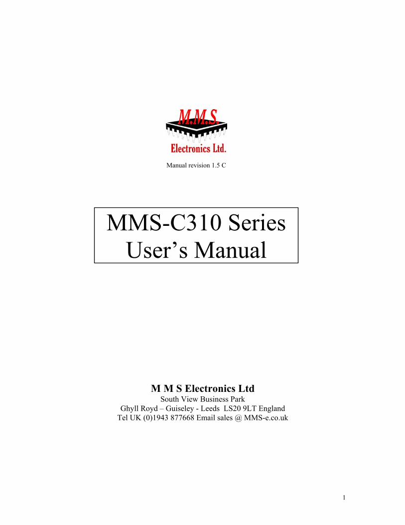
14
P4.0 7 CMSR0 LCD & keypad data line. pl9 pin 8 P4.1 8 CMSR1 LCD & keypad data line. pl9 pin 7 P4.2 9 CMSR2 LCD & keypad data line. pl9 pin 9 P4.3 10 CMSR3 LCD & keypad data line. pl9 pin 10 P4.4 11 CMSR4 , LCDE LCD enable. pl9 pin 6 P4.5 12 CMSR5 , LCDRW LCD read/write. pl9 pin 5 P4.6 13 CMT0 , LCDRS LCD data/instruction. pl9 pin 4 P4.7 14 CMT1 , KEYPOE Keypad output enable. P5.0 1 ADCO Analogue input. Connector AD.1 P5.1 68 ADC1 Analogue input. Connector AD.2 P5.2 67 ADC2 Analogue input. Connector AD.3 P5.3 66 ADC3 Analogue input. Connector AD.4 P5.4 65 ADC4 Analogue input. Connector AD.5 P5.5 64 ADC5 Analogue input. Not connected. P5.6 63 ADC6 Analogue input. Not connected. P5.7 62 ADC7 Analogue input. Not connected.

15
The Input, output and power supply terminals to the board are highly reliable and removable. This allows for a fast control board change without the need to rewire. All terminal pins are numbered and each of the connectors have a different pin out so no damage to the board could occur if a connector is wrongly inserted. Terminal Description OUTPUTS Pin 1 .. 3 : Relay outputs 5Amp max. (The relays are not fitted as standard) Pin 4 .. 7 : Relay outputs 1Amp max. Pin 8.. 23 : Transistor output 0.5 amp max. Pin 24 : Suppresser diode connection for output pins 8 .. 23. Pin 25..32 : Transistor output 0.5 amp max. Pin 33 : Suppresser diode connection for output pins 25..32. Pin 34..41 : Transistor output 0.5 amp max. Pin 42 : Suppresser diode connection for output pins 34..41 PL1 rel + : Coil supply voltage for the on board relays. PL1 com 1/3 : Common switch side of relay 1, 2 and 3. PL1 com 4/7 : Common switch of relay 4, 5, 6 and 7 PL3 pw0 : opto-isolated pulse width mode output, pwm0 PL3 pw1 : opto-isolated pulse width mode output, pwm1 INPUTS Pin 50..65 : 16 opto isolated inputs. Pin 66..69 : 4 opto isolated inputs or interrupts. SUPPLY PL2 P24 : + supply to opto-isolated I/O. Normally 12, 15 or 24 Volt. PL2 Pgnd : Gnd connection of supply to opto-isolated I/O. PL2 : Not connected. (From Iss7 this connection is Earth ) PL2 Gnd : Gnd logic supply (5 volt GND) PL2 +5V : + 5Volt logic supply.
Description of the control board connectors.
16
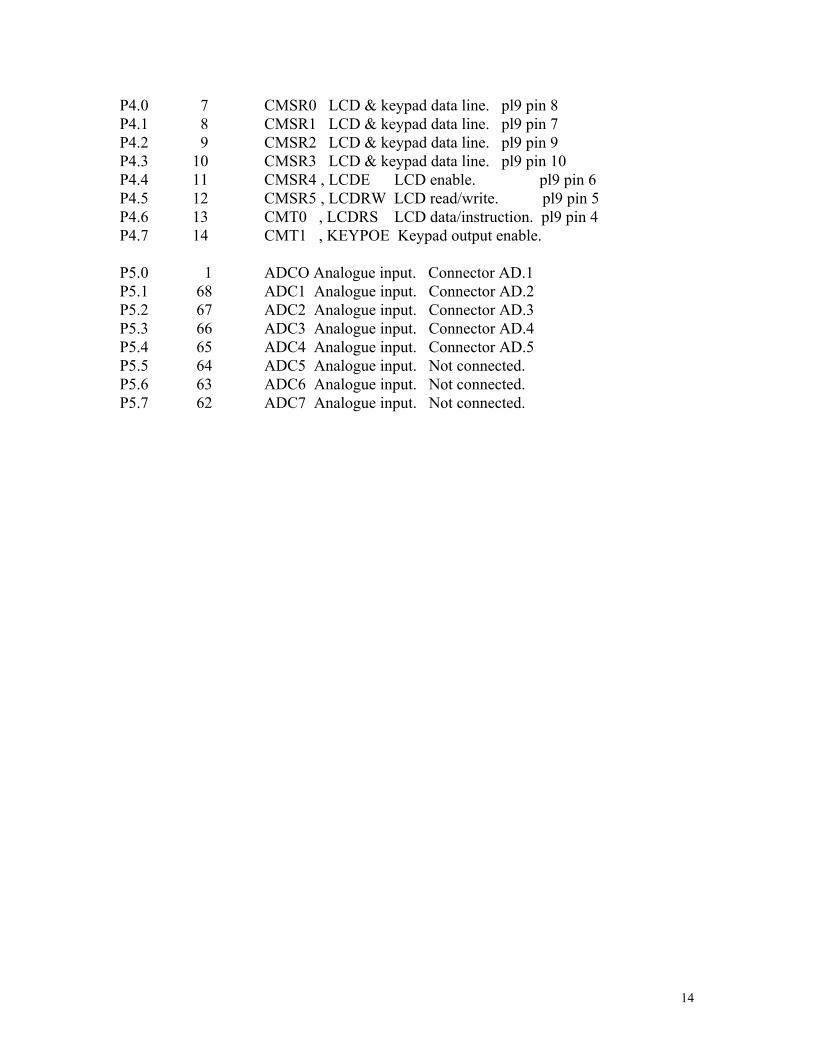
REG1 : This is the connection for a 3 pin regulator. 24, 15 or 12Volt to 5volt. LM340T or Switchmode PowerTrends PT78ST105V KEYPAD PL4 : Keypad 4*4 matrix, different pin connections then PL5 (Not on Iss 7) PL5 : Keypad 4*4 matrix, different pin connections then PL4 (default) SERIAL PORT The serial port allows program download or connection of a display with touch pad. For example: LCD panel 16 01607 (available from www.mms-e.co.uk) PL6 pin 1 : Connected to P GND PL6 pin 2 : RS232 serial out 1 , from RS232 converter to Ic1 pin 25 PL6 pin 3 : RS232 serial in 1 , from RS232 converter to Ic1 pin 24 PL6 pin 4 : RS232 serial out 2 , from RS232 converter to Ic1 pin 23 PL6 pin 5 : RS232 serial in 2 , from RS232 converter to Ic1 pin 22 PL6 pin 6 : PL6 pin 7 : Logic ground PL6 pin 8 : Not connected. PL6 pin 9 : Not connected. LCD port This port is TTL level and can also be used to connect other devices. For example: 7 digital Smartec temperature sensors SMT160-30 (available from MMS-e). PL9 pin 1 : Gnd. PL9 pin 2 : 5 Volt. PL9 pin 3 : LCD contrast setting. PL9 pin 4 : LCD instruction/data line connected to Ic1 P4.6 pin 13 PL9 pin 5 : LCD read/write line connected to Ic 1 P4.5 pin 12 PL9 pin 6 : LCD enable line connected to Ic 1 P4.4 pin 11 PL9 pin 7 : LCD data line connected to Ic1 P4.1 pin 8 PL9 pin 8 : LCD data line connected to Ic1 P4.0 pin 7 PL9 pin 9 : LCD data line connected to Ic1 P4.2 pin 9 PL9 pin 10 : LCD data line connected to Ic1 P4.3 pin 10 PL10 : Digital potentiometer, Ic 13

17
PL11 : Digital potentiometer, Ic 13 PL12 : Digital potentiometer, Ic 13 EXP : Expansion port I2C interface. WD : When linked watch dog timer circuit is enabled. AD1 : Analogue input signal 1 AD2 : Analogue input signal 2 AD3 : Analogue input signal 3 AD4 : Analogue input signal 4 AD5 : Analogue input signal 5 Adsupp : Connection for an external analogue voltage supply if required.

18
Once the input and output drivers are put into a call a program can easily be written. On the development disk is a simple interrupt driven program that looks after the timers, reading of the inputs and selecting the outputs. Example: SETB KNIFE ;set knife output. A1 JB KNIFESW,A1 ;wait until knife sw input is made. MOV A,#010D MOV R0,#TIM2VAL CALL CALCATIM ;setup timer 2 = 1 sec SETB T2F ;start timer 2 A2 JB T2F,A2 ;wait for 1 sec when timer 2 finished. .... The following examples show the code for the input and output drivers. The way the inputs or outputs are controlled is dictated by the hardware on the control board. Various tested routines for your applications are available from MMS. 1. Set-up the 8255 peripheral and reset output pins 25 to 41. ;Set-up the 8255 peripheral, only initiate once. MOV A,#088h ;port a, port b,1/2 portC outputs, 1/2 portC inputs MOV DPTR,#6003h ;8255 mode control address MOVX @DPTR,A ;set mode control register with 88 ;Reset output 25 to 32. MOV A,#000h ;reset output port MOV DPTR,#6002h ;8255 port b address MOVX @DPTR,A ;reset output 25 to 32 ;Reset output 34 to 41 MOV A,#000h ;reset output port MOV DPTR,#6000h ;8255 portA address MOVX @DPTR,A ;reset output 34 to 41 2. Use of output 1 to 23 with serial driver UCN5841. MOV A,#000h ;Reset outputs 16 to 23. CALL SETC ;Call routine that loads the shift register in the output driver. MOV A,#000h ;Reset outputs 8 to 15. CALL SETC ;Call routine that loads the shift register in the output driver. MOV A,#000h ;Reset output 1 to 7. CALL SETC ;Call routine that loads the shift register in the output driver. CALL SETDEL ;Call time delay between the clock & strobe pulse. CALL SETDEL CLR P1.5 ;Enable stobe pin to output driver. CALL SETDEL ;Call time delay for min stobe puls on time. SETB P1.5 ;Disable strobe pin to output driver. ; continue here with main program ...
8051 ASM program examples

19
SETC MOV B,#008D ;shift 8 bits into the output register. CPL A ;bits are reversed through the opto-coupler circuit. SETC2 RLC A ;rotate MOV P1.3,C ;Set or reset the data pin to the output driver. CALL SETDEL ;Call time delay, min data setup time. CLR P1.4 ;Make clock low (high after opto coupler circuit). CALL SETDEL ;Call time delay, min data setup time after clock high. SETB P1.3 ;reset the data pin to the output driver. CALL SETDEL ;Call time delay for clock width. SETB P1.4 ;make clock high (low after opto coupler circuit). DJNZ B,SETC2 ;check if all 8 bits are shifted in output driver. RET DELAY PUSH B ;Save B onto the stack. MOV B,#040H ;Time delay = 40H * 0.75 ySec * 2 SETD_1 DJNZ B,SETD_1 ;Decrement B until 0. POP B ;Restore value in B RET ;Return from call. 3. Reading the input ports. The following code will read all 16 inputs (pin 50 to 65) and store the result in internal RAM. With the Boolean instruction set of the 8051 it is easy to control the program actions. NAME: CALL RINP USE : Read all 16 inputs and store result in scan1 and scan2 ram memory. RINP MOV DPTR,#6001H ;set address of the 8255 for input scan portC. CLR A MOVX @DPTR,A ;make all input scan lines low. MOV A,#00001000B ;make first scan line high,portC c-3. CALL SCANINP ;read the values of the input matrix on portC. ANL A,#11110000B ;ignore bits 0-3. MOV SCAN1,A ;store this result in internal RAM address scan1 (bit 7 - 4) MOV A,#00000100B ;make 2nd scan line high, portC c-2. CALL SCANINP ;read the values of the input matrix on portc. SWAP A ;swap acc so we do not overwrite previous data. (bit 0 -3) ANL A,#00001111B ;ignore bits 4-7. ORL A,SCAN1 ;OR new scan from bits 0-3 and 4-7. MOV SCAN1,A ;store this result in internal RAM address scan1. (0-3) MOV A,#00000010B ;make 3rd scan line high, portc-3. CALL SCANINP ;read the values of the input matrix on portC. ANL A,#11110000B ;ignore bit 0-3. MOV SCAN2,A ;store this result in internal RAM address scan2. (7-4). MOV A,#00000001B ;make 3rd scan line high. CALL SCANINP ;read the values of the input matrix on portC. SWAP A ;swapp acc so we do not overwrite previous data. (bit 0-3) ANL A,#00001111B ;ignore bits 4-7. ORL A,SCAN2 ;OR new scan from bits 0-3 and 4-7. MOV SCAN2,A ;store this result in internal RAM address scan2. (0-3) CLR A MOVX @DPTR,A ;reset all input scan lines. RET ;return from call.
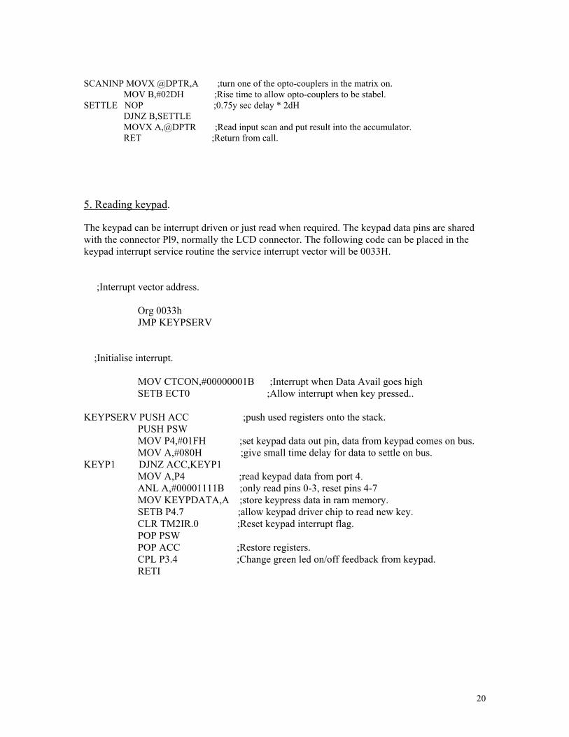
20
SCANINP MOVX @DPTR,A ;turn one of the opto-couplers in the matrix on. MOV B,#02DH ;Rise time to allow opto-couplers to be stabel. SETTLE NOP ;0.75y sec delay * 2dH DJNZ B,SETTLE MOVX A,@DPTR ;Read input scan and put result into the accumulator. RET ;Return from call. 5. Reading keypad. The keypad can be interrupt driven or just read when required. The keypad data pins are shared with the connector Pl9, normally the LCD connector. The following code can be placed in the keypad interrupt service routine the service interrupt vector will be 0033H. ;Interrupt vector address. Org 0033h JMP KEYPSERV ;Initialise interrupt. MOV CTCON,#00000001B ;Interrupt when Data Avail goes high SETB ECT0 ;Allow interrupt when key pressed.. KEYPSERV PUSH ACC ;push used registers onto the stack. PUSH PSW MOV P4,#01FH ;set keypad data out pin, data from keypad comes on bus. MOV A,#080H ;give small time delay for data to settle on bus. KEYP1 DJNZ ACC,KEYP1 MOV A,P4 ;read keypad data from port 4. ANL A,#00001111B ;only read pins 0-3, reset pins 4-7 MOV KEYPDATA,A ;store keypress data in ram memory. SETB P4.7 ;allow keypad driver chip to read new key. CLR TM2IR.0 ;Reset keypad interrupt flag. POP PSW POP ACC ;Restore registers. CPL P3.4 ;Change green led on/off feedback from keypad. RETI

21
Two serial outputs and two serial input ports are available on the control board and may be used to connect to computers, instruments, printers, modems and other MMS control boards. The serial line driver/receiver meets all RS232C and V28/V24 communication interfaces all from a single 5 Volt supply. The maximum usable baud rate is 19200 baud. The 80C552 two serial ports are full duplex and can transmit and receive simultaneously. This serial port is also received buffered. The serial port can also be set-up for multiprocessor communications. For more details read the 80c552 micro-controller user manual. If high and accurate baud rates need to be achieved then the processor crystal may need to be changed for your chosen baud rate. The EXP connector on the board is the output from the I2C bus and also SIO1 of the serial bus. SDA and SCL is used to transfer information between devices connected to this bus. The main uses are: Bi-directional data transfer between master & slave. This could be multiple MMS cards or other expansion boards with I2C bus. The I2C bus may be used for test and diagnostic purposes.
RS 232 Communication.
I2C Serial I/O

22
Please complete this form if you discover any software or hardware problems, documentation problems, or would like to suggest product enhancements. Hardware problem Software problem Documentation problem Product enhancement Date : Product : Serial # : Name : Company : Address : Phone : Fax : Please describe the problem, how to reproduce it and suggested correction. Or, describe enhancements that you would like to see added to this product. - - - - - - - - - - - - - Send or fax to MMS Electronics 01943 877 668. www.mms-e.co.uk
Problem report and comment form.