Embed Size (px)
Citation preview
MSP430F5338, MSP430F5336MSP430F5335, MSP430F5333
www.ti.com SLAS721C –AUGUST 2010–REVISED AUGUST 2013
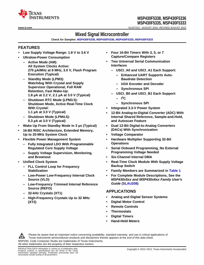
Mixed Signal MicrocontrollerCheck for Samples: MSP430F5338, MSP430F5336, MSP430F5335, MSP430F5333
1FEATURES23• Low Supply Voltage Range: 1.8 V to 3.6 V • Four 16-Bit Timers With 3, 5, or 7
Capture/Compare Registers• Ultralow-Power Consumption• Two Universal Serial Communication– Active Mode (AM):
InterfacesAll System Clocks Active:270 µA/MHz at 8 MHz, 3.0 V, Flash Program – USCI_A0 and USCI_A1 Each Support:Execution (Typical) – Enhanced UART Supports Auto-
– Standby Mode (LPM3): Baudrate DetectionWatchdog With Crystal and Supply – IrDA Encoder and DecoderSupervisor Operational, Full RAM – Synchronous SPIRetention, Fast Wake-Up:
– USCI_B0 and USCI_B1 Each Support:1.8 µA at 2.2 V, 2.1 µA at 3.0 V (Typical)– I2C– Shutdown RTC Mode (LPM3.5):– Synchronous SPIShutdown Mode, Active Real-Time Clock
With Crystal: • Integrated 3.3-V Power System1.1 µA at 3.0 V (Typical) • 12-Bit Analog-to-Digital Converter (ADC) With
– Shutdown Mode (LPM4.5): Internal Shared Reference, Sample-and-Hold,0.3 µA at 3.0 V (Typical) and Autoscan Feature
• Wake Up From Standby Mode in 3 µs (Typical) • Dual 12-Bit Digital-to-Analog Converters(DACs) With Synchronization• 16-Bit RISC Architecture, Extended Memory,
Up to 20-MHz System Clock • Voltage Comparator• Flexible Power Management System • Hardware Multiplier Supporting 32-Bit
Operations– Fully Integrated LDO With ProgrammableRegulated Core Supply Voltage • Serial Onboard Programming, No External
Programming Voltage Needed– Supply Voltage Supervision, Monitoring,and Brownout • Six-Channel Internal DMA
• Unified Clock System • Real-Time Clock Module With Supply VoltageBackup Switch– FLL Control Loop for Frequency
Stabilization • Family Members are Summarized in Table 1– Low-Power Low-Frequency Internal Clock • For Complete Module Descriptions, See the
Source (VLO) MSP430x5xx and MSP430x6xx Family User'sGuide (SLAU208)– Low-Frequency Trimmed Internal Reference
Source (REFO)APPLICATIONS– 32-kHz Crystals (XT1)• Analog and Digital Sensor Systems– High-Frequency Crystals Up to 32 MHz• Digital Motor Control(XT2)• Remote Controls• Thermostats• Digital Timers• Hand-Held Meters
1
Please be aware that an important notice concerning availability, standard warranty, and use in critical applications ofTexas Instruments semiconductor products and disclaimers thereto appears at the end of this data sheet.
2MSP430, Code Composer Studio are trademarks of Texas Instruments.3All other trademarks are the property of their respective owners.PRODUCTION DATA information is current as of publication date. Copyright © 2010–2013, Texas Instruments IncorporatedProducts conform to specifications per the terms of the TexasInstruments standard warranty. Production processing does notnecessarily include testing of all parameters.
MSP430F5338, MSP430F5336MSP430F5335, MSP430F5333SLAS721C –AUGUST 2010–REVISED AUGUST 2013 www.ti.com
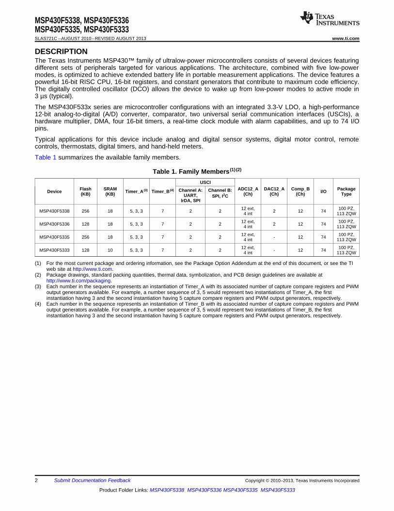
DESCRIPTIONThe Texas Instruments MSP430™ family of ultralow-power microcontrollers consists of several devices featuringdifferent sets of peripherals targeted for various applications. The architecture, combined with five low-powermodes, is optimized to achieve extended battery life in portable measurement applications. The device features apowerful 16-bit RISC CPU, 16-bit registers, and constant generators that contribute to maximum code efficiency.The digitally controlled oscillator (DCO) allows the device to wake up from low-power modes to active mode in3 µs (typical).
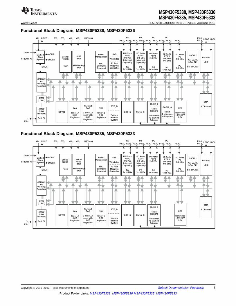
The MSP430F533x series are microcontroller configurations with an integrated 3.3-V LDO, a high-performance12-bit analog-to-digital (A/D) converter, comparator, two universal serial communication interfaces (USCIs), ahardware multiplier, DMA, four 16-bit timers, a real-time clock module with alarm capabilities, and up to 74 I/Opins.
Typical applications for this device include analog and digital sensor systems, digital motor control, remotecontrols, thermostats, digital timers, and hand-held meters.
Table 1 summarizes the available family members.
Table 1. Family Members (1) (2)
USCIFlash SRAM ADC12_A DAC12_A Comp_B PackageChannel A: Channel B:Device Timer_A (3) Timer_B (4) I/O(KB) (KB) (Ch) (Ch) (Ch) TypeUART, SPI, I2C
IrDA, SPI
12 ext, 100 PZ,MSP430F5338 256 18 5, 3, 3 7 2 2 2 12 744 int 113 ZQW
12 ext, 100 PZ,MSP430F5336 128 18 5, 3, 3 7 2 2 2 12 744 int 113 ZQW
12 ext, 100 PZ,MSP430F5335 256 18 5, 3, 3 7 2 2 - 12 744 int 113 ZQW
12 ext, 100 PZ,MSP430F5333 128 10 5, 3, 3 7 2 2 - 12 744 int 113 ZQW
(1) For the most current package and ordering information, see the Package Option Addendum at the end of this document, or see the TIweb site at http://www.ti.com.
(2) Package drawings, standard packing quantities, thermal data, symbolization, and PCB design guidelines are available athttp://www.ti.com/packaging.
(3) Each number in the sequence represents an instantiation of Timer_A with its associated number of capture compare registers and PWMoutput generators available. For example, a number sequence of 3, 5 would represent two instantiations of Timer_A, the firstinstantiation having 3 and the second instantiation having 5 capture compare registers and PWM output generators, respectively.
(4) Each number in the sequence represents an instantiation of Timer_B with its associated number of capture compare registers and PWMoutput generators available. For example, a number sequence of 3, 5 would represent two instantiations of Timer_B, the firstinstantiation having 3 and the second instantiation having 5 capture compare registers and PWM output generators, respectively.
2 Submit Documentation Feedback Copyright © 2010–2013, Texas Instruments Incorporated
Product Folder Links: MSP430F5338 MSP430F5336 MSP430F5335 MSP430F5333
UnifiedClock
System
256KB128KB
Flash
18KB/10KBRAM
+8B BackupRAMMCLK
ACLK
SMCLK
I/O PortsP1/P2
2×8 I/OsInterrupt
Capability
PA1×16 I/Os
CPUXV2and
WorkingRegisters
EEM(L: 8+2)
XIN XOUT
JTAG/SBW
Interface/
Port PJ
PA PB PC PD
DMA
6 Channel
XT2IN
XT2OUT
PowerManagement
LDOSVM/SVSBrownout
SYS
Watchdog
P2 PortMapping
Controller
I/O PortsP3/P4
2×8 I/OsInterrupt
Capability
PB1×16 I/Os
I/O PortsP5/P6
2×8 I/Os
PC1×16 I/Os
I/O PortsP7/P8
1×6 I/Os
PD1×14 I/Os
1×8 I/Os
I/O PortsP9
1×8 I/Os
PE1×8 I/Os
MPY32
TA0
Timer_A5 CC
Registers
TA1 andTA2
2 Timer_Aeach with
3 CCRegisters
TB0
Timer_B7 CC
Registers
CRC16
USCI0,1
Ax: UART,IrDA, SPI
Bx: SPI, I2C
ADC12_A
200 KSPS
16 Channels(12 ext/4 int)
Autoscan
12 Bit
DVCC DVSS AVCC AVSS
P1.x P2.x P3.x P4.x P5.x P6.x P7.x P8.x P9.xRST/NMI
REF
Reference1.5V, 2.0V,
2.5V
Comp_B
PJ.x
RTC_B
BatteryBackupSystem
PU Port
LDO
PU.0PU.1
LDOO LDOI
UnifiedClock
System
256KB128KB
FlashMCLK
ACLK
SMCLK
I/O PortsP1/P2
2×8 I/OsInterrupt
Capability
PA1×16 I/Os
CPUXV2and
WorkingRegisters
EEM(L: 8+2)
XIN XOUT
JTAG/SBW
Interface/
Port PJ
PA PB PC PD
DMA
6 Channel
XT2IN
XT2OUT
PowerManagement
LDOSVM/SVSBrownout
SYS
Watchdog
P2 PortMapping
Controller
I/O PortsP3/P4
2×8 I/OsInterrupt
Capability
PB1×16 I/Os
I/O PortsP5/P6
2×8 I/Os
PC1×16 I/Os
I/O PortsP7/P8
1×6 I/Os
PD1×14 I/Os
1×8 I/Os
I/O PortsP9
1×8 I/Os
PE1×8 I/Os
MPY32
TA0
Timer_A5 CC
Registers
TA1 andTA2
2 Timer_Aeach with
3 CCRegisters
TB0
Timer_B7 CC
Registers
RTC_B
BatteryBackupSystem
CRC16
USCI0,1
Ax: UART,IrDA, SPI
Bx: SPI, I2C
ADC12_A
200 KSPS
16 Channels(12 ext/4 int)
Autoscan
12 Bit
DVCC DVSS AVCC AVSS
P1.x P2.x P3.x P4.x P5.x P6.x P7.x P8.x P9.xRST/NMI
REF
Reference1.5V, 2.0V,
2.5V
DAC12_A
12 bit2 channelsvoltage out
Comp_B
PJ.x
18KBRAM
+8B BackupRAM
PU Port
LDO
PU.0PU.1
LDOO LDOI
MSP430F5338, MSP430F5336MSP430F5335, MSP430F5333
www.ti.com SLAS721C –AUGUST 2010–REVISED AUGUST 2013
Functional Block Diagram, MSP430F5338, MSP430F5336
Functional Block Diagram, MSP430F5335, MSP430F5333
Copyright © 2010–2013, Texas Instruments Incorporated Submit Documentation Feedback 3
Product Folder Links: MSP430F5338 MSP430F5336 MSP430F5335 MSP430F5333
1
2
3
4
5
6
7
8
9
10
11
12
13
14
15
16
17
18
19
20
21
22
23
24
25
76
77
78
79
80
81
82
83
84
85
86
87
88
89
90
91
92
93
94
95
96
97
98
99
100
75
74
73
72
71
70
69
68
67
66
65
64
63
62
61
60
59
58
57
56
55
54
53
52
51
50
49
48
47
46
45
44
43
42
41
40
39
38
37
36
35
34
33
32
31
30
29
28
27
26
P6.4/CB4/A4
P6.5/CB5/A5
P6.6/CB6/A6/DAC0
P6.7/CB7/A7/DAC1
P7.4/CB8/A12
P7.5/CB9/A13
P7.6/CB10/A14/DAC0
P7.7/CB11/A15/DAC1
P5.0/VREF+/VeREF+
P5.1/VREF−/VeREF−
AVCC1
AVSS1
XIN
XOUT
DVCC1
DV
SS
1
VC
OR
E
P5.2
DV
SS
DN
C
P5
.3
P9.7
P9.6
P9.5
P9.4
P9.3
P9.2
P9.1
P9.0
P8.7
P8.6/UCB1SOMI/UCB1SCL
P8.5/UCB1SIMO/UCB1SDA
DVCC2
DVSS2
P2.0/P2MAP0
MSP430F5338MSP430F5336
PZ PACKAGE(TOP VIEW)
P6.3
/CB
3/A
3
P6.2
/CB
2/A
2
P6.1
/CB
1/A
1
P6.0
/CB
0/A
0
RS
T/N
MI/S
BW
TD
IO
PJ.3
/TC
K
PJ.2
/TM
S
PJ.1
/TD
I/T
CLK
PJ.0
/TD
O
TE
ST
/SB
WT
CK
P7.3
/XT
2O
UT
P7.2
/XT
2IN
LD
OI
LD
OO
PU
.1
NC
PU
.0
VS
SU
NC
AV
SS
3
P1.3
/TA
0.2
P1.4
/TA
0.3
AVSS2
P5.6/ADC12CLK/DMAE0
P5
.4
P5
.5
P1
.0/T
A0
CL
K/A
CL
K
P3
.0/T
A1
CL
K/C
BO
UT
P3
.1/T
A1
.0
P3
.2/T
A1
.1
P1
.6/T
A0
.1
P1
.7/T
A0
.2
P1
.1/T
A0
.0
P1
.2/T
A0
.1
P1
.5/T
A0
.4
P3
.3/T
A1
.2
P3
.4/T
A2
CL
K/S
MC
LK
P3
.5/T
A2
.0
P3
.6/T
A2
.1
P3
.7/T
A2
.2
P4
.0/T
B0
.0
P4.2/TB0.2
P4.1/TB0.1
P4.4/TB0.4
P4.3/TB0.3
P4.6/TB0.6
P4.5/TB0.5
P8.0/TB0CLK
P4.7/TB0OUTH/SVMOUT
P8.4/UCB1CLK/UCA1STE
VB
AK
P2.1/P2MAP1
P2.2/P2MAP2
P2.3/P2MAP3
P2.4/P2MAP4
P2.5/P2MAP5
P2.6/P2MAP6
P2.7/P2MAP7
DV
CC
3
DV
SS
3
VB
AT
P5.7
/RT
CC
LK
P8.1/UCB1STE/UCA1CLK
P8.2/UCA1TXD/UCA1SIMO
P8.3/UCA1RXD/UCA1SOMI
MSP430F5338, MSP430F5336MSP430F5335, MSP430F5333SLAS721C –AUGUST 2010–REVISED AUGUST 2013 www.ti.com
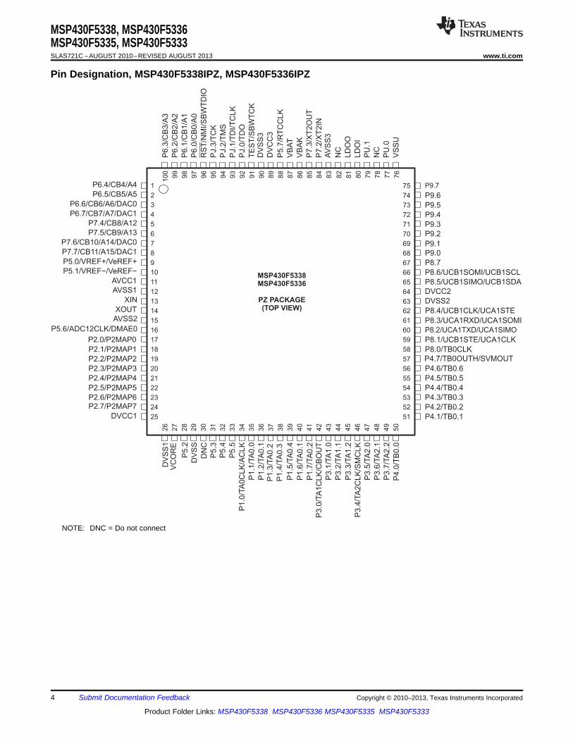
Pin Designation, MSP430F5338IPZ, MSP430F5336IPZ
NOTE: DNC = Do not connect
4 Submit Documentation Feedback Copyright © 2010–2013, Texas Instruments Incorporated
Product Folder Links: MSP430F5338 MSP430F5336 MSP430F5335 MSP430F5333
1
2
3
4
5
6
7
8
9
10
11
12
13
14
15
16
17
18
19
20
21
22
23
24
25
76
77
78
79
80
81
82
83
84
85
86
87
88
89
90
91
92
93
94
95
96
97
98
99
100
75
74
73
72
71
70
69
68
67
66
65
64
63
62
61
60
59
58
57
56
55
54
53
52
51
50
49
48
47
46
45
44
43
42
41
40
39
38
37
36
35
34
33
32
31
30
29
28
27
26
P6.4/CB4/A4
P6.5/CB5/A5
P6.6/CB6/A6
P6.7/CB7/A7
P7.4/CB8/A12
P7.5/CB9/A13
P7.6/CB10/A14
P7.7/CB11/A15
P5.0/VREF+/VeREF+
P5.1/VREF−/VeREF−
AVCC1
AVSS1
XIN
XOUT
DVCC1
DV
SS
1
VC
OR
E
P5.2
DV
SS
DN
C
P5
.3
P9.7
P9.6
P9.5
P9.4
P9.3
P9.2
P9.1
P9.0
P8.7
P8.6/UCB1SOMI/UCB1SCL
P8.5/UCB1SIMO/UCB1SDA
DVCC2
DVSS2
P2.0/P2MAP0
MSP430F5335MSP430F5333
PZ PACKAGE(TOP VIEW)
P6.3
/CB
3/A
3
P6.2
/CB
2/A
2
P6.1
/CB
1/A
1
P6.0
/CB
0/A
0
RS
T/N
MI/S
BW
TD
IO
PJ.3
/TC
K
PJ.2
/TM
S
PJ.1
/TD
I/T
CLK
PJ.0
/TD
O
TE
ST
/SB
WT
CK
P7.3
/XT
2O
UT
P7.2
/XT
2IN
LD
OI
LD
OO
PU
.1
NC
PU
.0
VS
SU
NC
AV
SS
3
P1.3
/TA
0.2
P1.4
/TA
0.3
AVSS2
P5.6/ADC12CLK/DMAE0
P5
.4
P5
.5
P1
.0/T
A0
CL
K/A
CL
K
P3
.0/T
A1
CL
K/C
BO
UT
P3
.1/T
A1
.0
P3
.2/T
A1
.1
P1
.6/T
A0
.1
P1
.7/T
A0
.2
P1
.1/T
A0
.0
P1
.2/T
A0
.1
P1
.5/T
A0
.4
P3
.3/T
A1
.2
P3
.4/T
A2
CL
K/S
MC
LK
P3
.5/T
A2
.0
P3
.6/T
A2
.1
P3
.7/T
A2
.2
P4
.0/T
B0
.0
P4.2/TB0.2
P4.1/TB0.1
P4.4/TB0.4
P4.3/TB0.3
P4.6/TB0.6
P4.5/TB0.5
P8.0/TB0CLK
P4.7/TB0OUTH/SVMOUT
P8.4/UCB1CLK/UCA1STE
VB
AK
P2.1/P2MAP1
P2.2/P2MAP2
P2.3/P2MAP3
P2.4/P2MAP4
P2.5/P2MAP5
P2.6/P2MAP6
P2.7/P2MAP7
DV
CC
3
DV
SS
3
VB
AT
P5.7
/RT
CC
LK
P8.1/UCB1STE/UCA1CLK
P8.2/UCA1TXD/UCA1SIMO
P8.3/UCA1RXD/UCA1SOMI
MSP430F5338, MSP430F5336MSP430F5335, MSP430F5333
www.ti.com SLAS721C –AUGUST 2010–REVISED AUGUST 2013
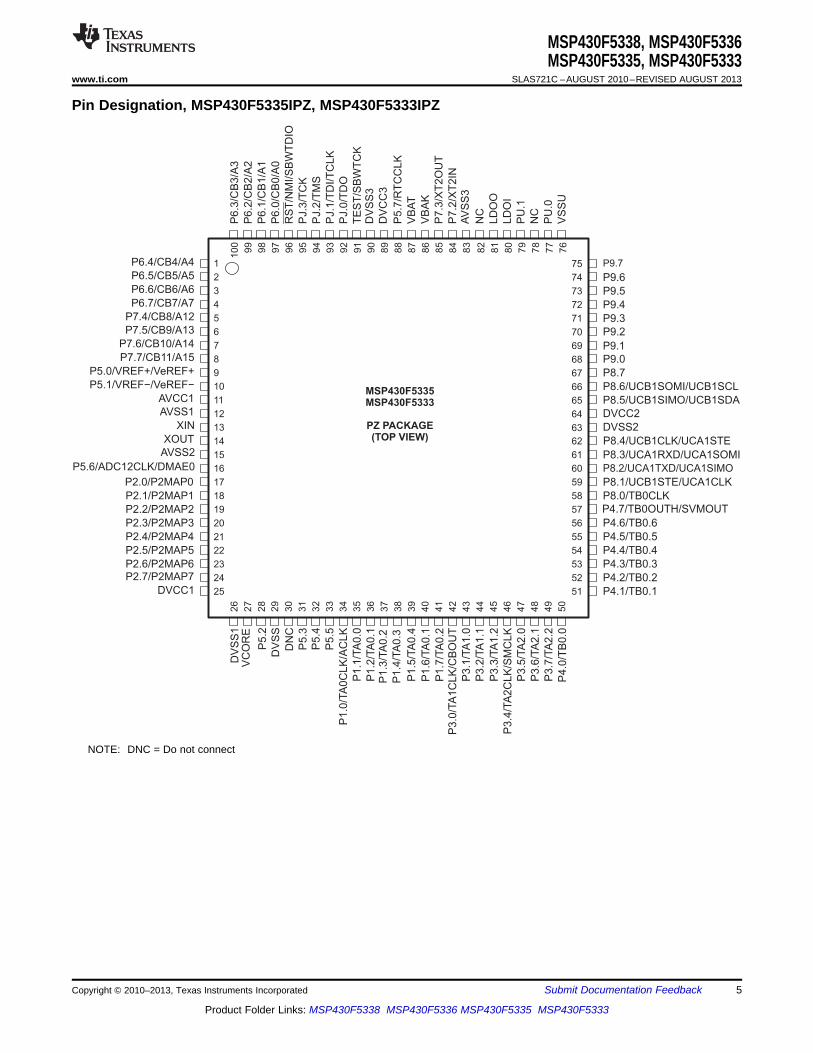
Pin Designation, MSP430F5335IPZ, MSP430F5333IPZ
NOTE: DNC = Do not connect
Copyright © 2010–2013, Texas Instruments Incorporated Submit Documentation Feedback 5
Product Folder Links: MSP430F5338 MSP430F5336 MSP430F5335 MSP430F5333
A1 A2 A3 A4 A5 A6 A7 A8 A9 A10 A11 A12
B1 B2 B3 B4 B5 B6 B7 B8 B9 B10 B11 B12
C1 C2 C3 C11 C12
D1 D2 D4 D5 D6 D7 D8 D9 D11 D12
E1 E2 E4 E5 E6 E7 E8 E9 E11 E12
F1 F2 F4 F5 F8 F9 F11 F12
G1 G2 G4 G5 G8 G9 G11 G12
J1 J2 J4 J5 J6 J7 J8 J9 J11 J12
H1 H2 H4 H5 H6 H7 H8 H9 H11 H12
K1 K2 K11 K12
L1 L2 L3 L4 L5 L6 L7 L8 L9 L10 L11 L12
M1 M2 M3 M5 M6 M7 M8 M9 M10 M11 M12M4
ZQW PACKAGE(TOP VIEW)
MSP430F5338, MSP430F5336MSP430F5335, MSP430F5333SLAS721C –AUGUST 2010–REVISED AUGUST 2013 www.ti.com
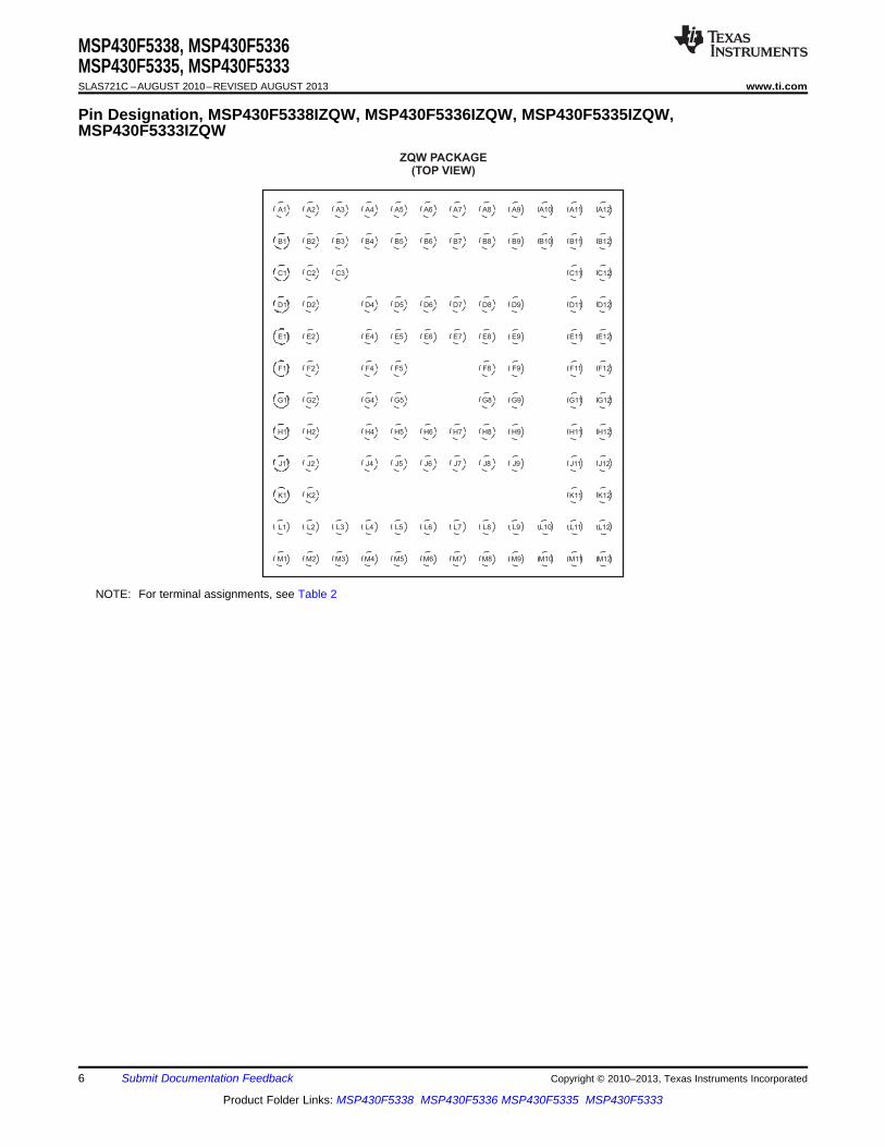
Pin Designation, MSP430F5338IZQW, MSP430F5336IZQW, MSP430F5335IZQW,MSP430F5333IZQW
NOTE: For terminal assignments, see Table 2
6 Submit Documentation Feedback Copyright © 2010–2013, Texas Instruments Incorporated
Product Folder Links: MSP430F5338 MSP430F5336 MSP430F5335 MSP430F5333
MSP430F5338, MSP430F5336MSP430F5335, MSP430F5333
www.ti.com SLAS721C –AUGUST 2010–REVISED AUGUST 2013
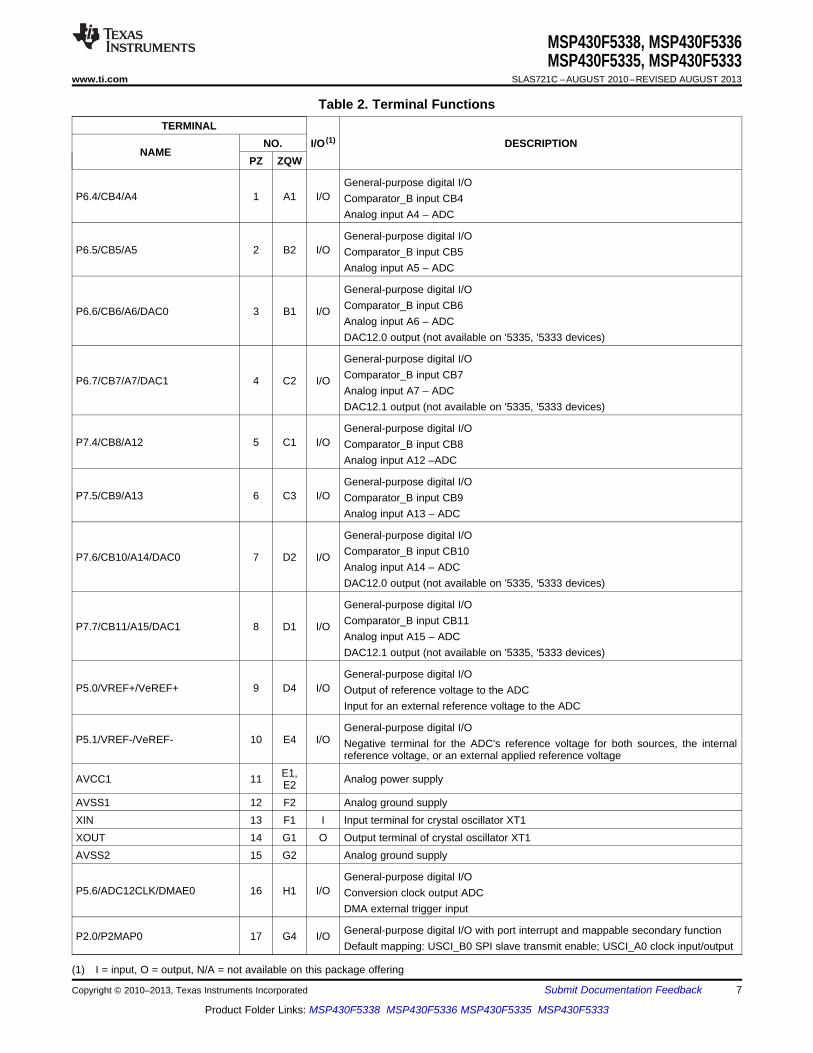
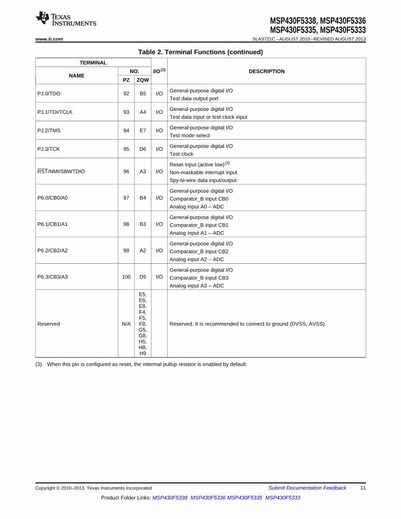
Table 2. Terminal FunctionsTERMINAL
NO. I/O (1) DESCRIPTIONNAME
PZ ZQW
General-purpose digital I/OP6.4/CB4/A4 1 A1 I/O Comparator_B input CB4
Analog input A4 – ADC
General-purpose digital I/OP6.5/CB5/A5 2 B2 I/O Comparator_B input CB5
Analog input A5 – ADC
General-purpose digital I/OComparator_B input CB6P6.6/CB6/A6/DAC0 3 B1 I/OAnalog input A6 – ADCDAC12.0 output (not available on '5335, '5333 devices)
General-purpose digital I/OComparator_B input CB7P6.7/CB7/A7/DAC1 4 C2 I/OAnalog input A7 – ADCDAC12.1 output (not available on '5335, '5333 devices)
General-purpose digital I/OP7.4/CB8/A12 5 C1 I/O Comparator_B input CB8
Analog input A12 –ADC
General-purpose digital I/OP7.5/CB9/A13 6 C3 I/O Comparator_B input CB9
Analog input A13 – ADC
General-purpose digital I/OComparator_B input CB10P7.6/CB10/A14/DAC0 7 D2 I/OAnalog input A14 – ADCDAC12.0 output (not available on '5335, '5333 devices)
General-purpose digital I/OComparator_B input CB11P7.7/CB11/A15/DAC1 8 D1 I/OAnalog input A15 – ADCDAC12.1 output (not available on '5335, '5333 devices)
General-purpose digital I/OP5.0/VREF+/VeREF+ 9 D4 I/O Output of reference voltage to the ADC
Input for an external reference voltage to the ADC
General-purpose digital I/OP5.1/VREF-/VeREF- 10 E4 I/O Negative terminal for the ADC's reference voltage for both sources, the internal
reference voltage, or an external applied reference voltageE1,AVCC1 11 Analog power supplyE2
AVSS1 12 F2 Analog ground supplyXIN 13 F1 I Input terminal for crystal oscillator XT1XOUT 14 G1 O Output terminal of crystal oscillator XT1AVSS2 15 G2 Analog ground supply
General-purpose digital I/OP5.6/ADC12CLK/DMAE0 16 H1 I/O Conversion clock output ADC
DMA external trigger input
General-purpose digital I/O with port interrupt and mappable secondary functionP2.0/P2MAP0 17 G4 I/ODefault mapping: USCI_B0 SPI slave transmit enable; USCI_A0 clock input/output
(1) I = input, O = output, N/A = not available on this package offering
Copyright © 2010–2013, Texas Instruments Incorporated Submit Documentation Feedback 7
Product Folder Links: MSP430F5338 MSP430F5336 MSP430F5335 MSP430F5333
MSP430F5338, MSP430F5336MSP430F5335, MSP430F5333SLAS721C –AUGUST 2010–REVISED AUGUST 2013 www.ti.com
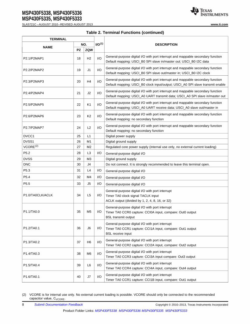
Table 2. Terminal Functions (continued)TERMINAL
NO. I/O (1) DESCRIPTIONNAME
PZ ZQW
General-purpose digital I/O with port interrupt and mappable secondary functionP2.1/P2MAP1 18 H2 I/ODefault mapping: USCI_B0 SPI slave in/master out; USCI_B0 I2C data
General-purpose digital I/O with port interrupt and mappable secondary functionP2.2/P2MAP2 19 J1 I/ODefault mapping: USCI_B0 SPI slave out/master in; USCI_B0 I2C clock
General-purpose digital I/O with port interrupt and mappable secondary functionP2.3/P2MAP3 20 H4 I/ODefault mapping: USCI_B0 clock input/output; USCI_A0 SPI slave transmit enable
General-purpose digital I/O with port interrupt and mappable secondary functionP2.4/P2MAP4 21 J2 I/ODefault mapping: USCI_A0 UART transmit data; USCI_A0 SPI slave in/master out
General-purpose digital I/O with port interrupt and mappable secondary functionP2.5/P2MAP5 22 K1 I/ODefault mapping: USCI_A0 UART receive data; USCI_A0 slave out/master in
General-purpose digital I/O with port interrupt and mappable secondary functionP2.6/P2MAP6 23 K2 I/ODefault mapping: no secondary function
General-purpose digital I/O with port interrupt and mappable secondary functionP2.7/P2MAP7 24 L2 I/ODefault mapping: no secondary function
DVCC1 25 L1 Digital power supplyDVSS1 26 M1 Digital ground supplyVCORE (2) 27 M2 Regulated core power supply (internal use only, no external current loading)
P5.2 28 L3 I/O General-purpose digital I/ODVSS 29 M3 Digital ground supplyDNC 30 J4 Do not connect. It is strongly recommended to leave this terminal open.
P5.3 31 L4 I/O General-purpose digital I/O
P5.4 32 M4 I/O General-purpose digital I/O
P5.5 33 J5 I/O General-purpose digital I/O
General-purpose digital I/O with port interruptP1.0/TA0CLK/ACLK 34 L5 I/O Timer TA0 clock signal TACLK input
ACLK output (divided by 1, 2, 4, 8, 16, or 32)
General-purpose digital I/O with port interruptP1.1/TA0.0 35 M5 I/O Timer TA0 CCR0 capture: CCI0A input, compare: Out0 output
BSL transmit output
General-purpose digital I/O with port interruptP1.2/TA0.1 36 J6 I/O Timer TA0 CCR1 capture: CCI1A input, compare: Out1 output
BSL receive input
General-purpose digital I/O with port interruptP1.3/TA0.2 37 H6 I/OTimer TA0 CCR2 capture: CCI2A input, compare: Out2 output
General-purpose digital I/O with port interruptP1.4/TA0.3 38 M6 I/OTimer TA0 CCR3 capture: CCI3A input compare: Out3 output
General-purpose digital I/O with port interruptP1.5/TA0.4 39 L6 I/OTimer TA0 CCR4 capture: CCI4A input, compare: Out4 output
General-purpose digital I/O with port interruptP1.6/TA0.1 40 J7 I/OTimer TA0 CCR1 capture: CCI1B input, compare: Out1 output
(2) VCORE is for internal use only. No external current loading is possible. VCORE should only be connected to the recommendedcapacitor value, CVCORE.
8 Submit Documentation Feedback Copyright © 2010–2013, Texas Instruments Incorporated
Product Folder Links: MSP430F5338 MSP430F5336 MSP430F5335 MSP430F5333
MSP430F5338, MSP430F5336MSP430F5335, MSP430F5333
www.ti.com SLAS721C –AUGUST 2010–REVISED AUGUST 2013
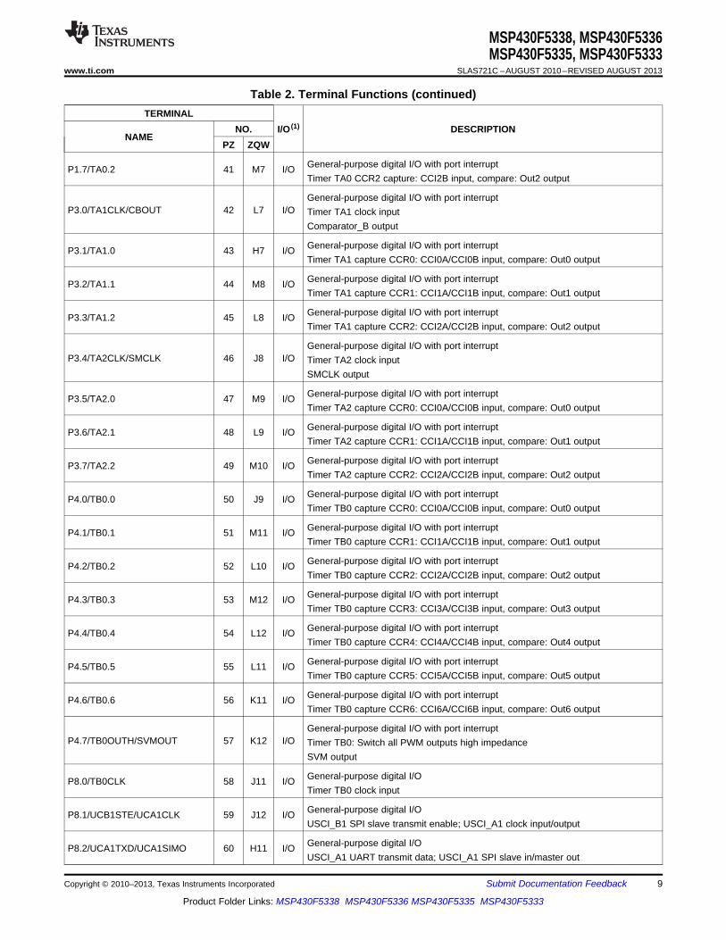
Table 2. Terminal Functions (continued)TERMINAL
NO. I/O (1) DESCRIPTIONNAME
PZ ZQW
General-purpose digital I/O with port interruptP1.7/TA0.2 41 M7 I/OTimer TA0 CCR2 capture: CCI2B input, compare: Out2 output
General-purpose digital I/O with port interruptP3.0/TA1CLK/CBOUT 42 L7 I/O Timer TA1 clock input
Comparator_B output
General-purpose digital I/O with port interruptP3.1/TA1.0 43 H7 I/OTimer TA1 capture CCR0: CCI0A/CCI0B input, compare: Out0 output
General-purpose digital I/O with port interruptP3.2/TA1.1 44 M8 I/OTimer TA1 capture CCR1: CCI1A/CCI1B input, compare: Out1 output
General-purpose digital I/O with port interruptP3.3/TA1.2 45 L8 I/OTimer TA1 capture CCR2: CCI2A/CCI2B input, compare: Out2 output
General-purpose digital I/O with port interruptP3.4/TA2CLK/SMCLK 46 J8 I/O Timer TA2 clock input
SMCLK output
General-purpose digital I/O with port interruptP3.5/TA2.0 47 M9 I/OTimer TA2 capture CCR0: CCI0A/CCI0B input, compare: Out0 output
General-purpose digital I/O with port interruptP3.6/TA2.1 48 L9 I/OTimer TA2 capture CCR1: CCI1A/CCI1B input, compare: Out1 output
General-purpose digital I/O with port interruptP3.7/TA2.2 49 M10 I/OTimer TA2 capture CCR2: CCI2A/CCI2B input, compare: Out2 output
General-purpose digital I/O with port interruptP4.0/TB0.0 50 J9 I/OTimer TB0 capture CCR0: CCI0A/CCI0B input, compare: Out0 output
General-purpose digital I/O with port interruptP4.1/TB0.1 51 M11 I/OTimer TB0 capture CCR1: CCI1A/CCI1B input, compare: Out1 output
General-purpose digital I/O with port interruptP4.2/TB0.2 52 L10 I/OTimer TB0 capture CCR2: CCI2A/CCI2B input, compare: Out2 output
General-purpose digital I/O with port interruptP4.3/TB0.3 53 M12 I/OTimer TB0 capture CCR3: CCI3A/CCI3B input, compare: Out3 output
General-purpose digital I/O with port interruptP4.4/TB0.4 54 L12 I/OTimer TB0 capture CCR4: CCI4A/CCI4B input, compare: Out4 output
General-purpose digital I/O with port interruptP4.5/TB0.5 55 L11 I/OTimer TB0 capture CCR5: CCI5A/CCI5B input, compare: Out5 output
General-purpose digital I/O with port interruptP4.6/TB0.6 56 K11 I/OTimer TB0 capture CCR6: CCI6A/CCI6B input, compare: Out6 output
General-purpose digital I/O with port interruptP4.7/TB0OUTH/SVMOUT 57 K12 I/O Timer TB0: Switch all PWM outputs high impedance
SVM output
General-purpose digital I/OP8.0/TB0CLK 58 J11 I/OTimer TB0 clock input
General-purpose digital I/OP8.1/UCB1STE/UCA1CLK 59 J12 I/OUSCI_B1 SPI slave transmit enable; USCI_A1 clock input/output
General-purpose digital I/OP8.2/UCA1TXD/UCA1SIMO 60 H11 I/OUSCI_A1 UART transmit data; USCI_A1 SPI slave in/master out
Copyright © 2010–2013, Texas Instruments Incorporated Submit Documentation Feedback 9
Product Folder Links: MSP430F5338 MSP430F5336 MSP430F5335 MSP430F5333
MSP430F5338, MSP430F5336MSP430F5335, MSP430F5333SLAS721C –AUGUST 2010–REVISED AUGUST 2013 www.ti.com
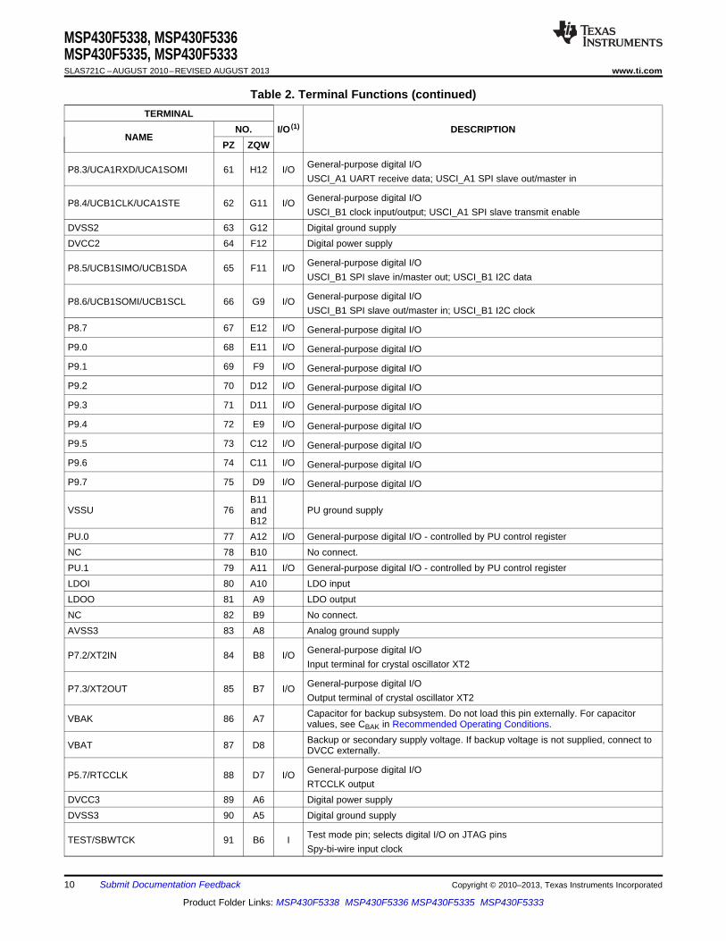
Table 2. Terminal Functions (continued)TERMINAL
NO. I/O (1) DESCRIPTIONNAME
PZ ZQW
General-purpose digital I/OP8.3/UCA1RXD/UCA1SOMI 61 H12 I/OUSCI_A1 UART receive data; USCI_A1 SPI slave out/master in
General-purpose digital I/OP8.4/UCB1CLK/UCA1STE 62 G11 I/OUSCI_B1 clock input/output; USCI_A1 SPI slave transmit enable
DVSS2 63 G12 Digital ground supplyDVCC2 64 F12 Digital power supply
General-purpose digital I/OP8.5/UCB1SIMO/UCB1SDA 65 F11 I/OUSCI_B1 SPI slave in/master out; USCI_B1 I2C data
General-purpose digital I/OP8.6/UCB1SOMI/UCB1SCL 66 G9 I/OUSCI_B1 SPI slave out/master in; USCI_B1 I2C clock
P8.7 67 E12 I/O General-purpose digital I/O
P9.0 68 E11 I/O General-purpose digital I/O
P9.1 69 F9 I/O General-purpose digital I/O
P9.2 70 D12 I/O General-purpose digital I/O
P9.3 71 D11 I/O General-purpose digital I/O
P9.4 72 E9 I/O General-purpose digital I/O
P9.5 73 C12 I/O General-purpose digital I/O
P9.6 74 C11 I/O General-purpose digital I/O
P9.7 75 D9 I/O General-purpose digital I/OB11
VSSU 76 and PU ground supplyB12
PU.0 77 A12 I/O General-purpose digital I/O - controlled by PU control registerNC 78 B10 No connect.PU.1 79 A11 I/O General-purpose digital I/O - controlled by PU control registerLDOI 80 A10 LDO inputLDOO 81 A9 LDO outputNC 82 B9 No connect.AVSS3 83 A8 Analog ground supply
General-purpose digital I/OP7.2/XT2IN 84 B8 I/OInput terminal for crystal oscillator XT2
General-purpose digital I/OP7.3/XT2OUT 85 B7 I/OOutput terminal of crystal oscillator XT2Capacitor for backup subsystem. Do not load this pin externally. For capacitorVBAK 86 A7 values, see CBAK in Recommended Operating Conditions.Backup or secondary supply voltage. If backup voltage is not supplied, connect toVBAT 87 D8 DVCC externally.
General-purpose digital I/OP5.7/RTCCLK 88 D7 I/ORTCCLK output
DVCC3 89 A6 Digital power supplyDVSS3 90 A5 Digital ground supply
Test mode pin; selects digital I/O on JTAG pinsTEST/SBWTCK 91 B6 ISpy-bi-wire input clock
10 Submit Documentation Feedback Copyright © 2010–2013, Texas Instruments Incorporated
Product Folder Links: MSP430F5338 MSP430F5336 MSP430F5335 MSP430F5333
MSP430F5338, MSP430F5336MSP430F5335, MSP430F5333
www.ti.com SLAS721C –AUGUST 2010–REVISED AUGUST 2013
Table 2. Terminal Functions (continued)TERMINAL
NO. I/O (1) DESCRIPTIONNAME
PZ ZQW
General-purpose digital I/OPJ.0/TDO 92 B5 I/OTest data output port
General-purpose digital I/OPJ.1/TDI/TCLK 93 A4 I/OTest data input or test clock input
General-purpose digital I/OPJ.2/TMS 94 E7 I/OTest mode select
General-purpose digital I/OPJ.3/TCK 95 D6 I/OTest clock
Reset input (active low) (3)
RST/NMI/SBWTDIO 96 A3 I/O Non-maskable interrupt inputSpy-bi-wire data input/output
General-purpose digital I/OP6.0/CB0/A0 97 B4 I/O Comparator_B input CB0
Analog input A0 – ADC
General-purpose digital I/OP6.1/CB1/A1 98 B3 I/O Comparator_B input CB1
Analog input A1 – ADC
General-purpose digital I/OP6.2/CB2/A2 99 A2 I/O Comparator_B input CB2
Analog input A2 – ADC
General-purpose digital I/OP6.3/CB3/A3 100 D5 I/O Comparator_B input CB3
Analog input A3 – ADCE5,E6,E8,F4,F5,
Reserved N/A F8, Reserved. It is recommended to connect to ground (DVSS, AVSS).G5,G8,H5,H8,H9
(3) When this pin is configured as reset, the intermal pullup resistor is enabled by default.
Copyright © 2010–2013, Texas Instruments Incorporated Submit Documentation Feedback 11
Product Folder Links: MSP430F5338 MSP430F5336 MSP430F5335 MSP430F5333
MSP430F5338, MSP430F5336MSP430F5335, MSP430F5333SLAS721C –AUGUST 2010–REVISED AUGUST 2013 www.ti.com
Development Tools Support
All MSP430™ microcontrollers are supported by a wide variety of software and hardware development tools.Tools are available from TI and various third parties. See them all at www.ti.com/msp430tools.
Hardware FeaturesSee the Code Composer Studio for MSP430 User's Guide (SLAU157) for details on the available features.
Break- Range LPMx.5MSP430 4-Wire 2-Wire Clock State Tracepoints Break- DebuggingArchitecture JTAG JTAG Control Sequencer Buffer(N) points SupportMSP430Xv2 Yes Yes 8 Yes Yes Yes Yes No
Recommended Hardware Options
Target Socket BoardsThe target socket boards allow easy programming and debugging of the device using JTAG. They also featureheader pin outs for prototyping. Target socket boards are orderable individually or as a kit with the JTAGprogrammer and debugger included. The following table shows the compatible target boards and the supportedpackages.
Package Target Board and Programmer Bundle Target Board Only100-pin LQFP (PZ) MSP-FET430U100C MSP-TS430PZ100C
Experimenter BoardsExperimenter Boards and Evaluation kits are available for some MSP430 devices. These kits feature additionalhardware components and connectivity for full system evaluation and prototyping. See www.ti.com/msp430toolsfor details.
Debugging and Programming ToolsHardware programming and debugging tools are available from TI and from its third party suppliers. See the fulllist of available tools at www.ti.com/msp430tools.
Production ProgrammersThe production programmers expedite loading firmware to devices by programming several devicessimultaneously.
Part Number PC Port Features ProviderMSP-GANG Serial and USB Program up to eight devices at a time. Works with PC or standalone. Texas Instruments
Recommended Software Options
Integrated Development EnvironmentsSoftware development tools are available from TI or from third parties. Open source solutions are also available.
This device is supported by Code Composer Studio™ IDE (CCS).
MSP430WareMSP430Ware is a collection of code examples, data sheets, and other design resources for all MSP430 devicesdelivered in a convenient package. In addition to providing a complete collection of existing MSP430 designresources, MSP430Ware also includes a high-level API called MSP430 Driver Library. This library makes it easyto program MSP430 hardware. MSP430Ware is available as a component of CCS or as a standalone package.
12 Submit Documentation Feedback Copyright © 2010–2013, Texas Instruments Incorporated
Product Folder Links: MSP430F5338 MSP430F5336 MSP430F5335 MSP430F5333

MSP430F5338, MSP430F5336MSP430F5335, MSP430F5333
www.ti.com SLAS721C –AUGUST 2010–REVISED AUGUST 2013
TI-RTOSTI-RTOS is a complete real-time operating system for the MSP430 microcontrollers. It combines a real-timemultitasking kernel SYS/BIOS with additional middleware components. TI-RTOS is available free of charge andprovided with full source code.
Command-Line ProgrammerMSP430 Flasher is an open-source, shell-based interface for programming MSP430 microcontrollers through aFET programmer or eZ430 using JTAG or Spy-Bi-Wire (SBW) communication. MSP430 Flasher can be used todownload binary files (.txt or .hex) files directly to the MSP430 Flash without the need for an IDE.
Community ResourcesThe following links connect to TI community resources. Linked contents are provided "AS IS" by the respectivecontributors. They do not constitute TI specifications and do not necessarily reflect TI's views; see TI's Terms ofUse.
TI E2E CommunityTI's Engineer-to-Engineer (E2E) Community. Created to foster collaboration among engineers. At e2e.ti.com, youcan ask questions, share knowledge, explore ideas, and help solve problems with fellow engineers.
TI Embedded Processors WikiTexas Instruments Embedded Processors Wiki. Established to help developers get started with embeddedprocessors from Texas Instruments and to foster innovation and growth of general knowledge about thehardware and software surrounding these devices.
Device and Development Tool Nomenclature
To designate the stages in the product development cycle, TI assigns prefixes to the part numbers of allMSP430™ MCU devices and support tools. Each MSP430™ MCU commercial family member has one of twoprefixes: MSP or XMS (for example, MSP430F5259). Texas Instruments recommends two of three possibleprefix designators for its support tools: MSP and MSPX. These prefixes represent evolutionary stages of productdevelopment from engineering prototypes (with XMS for devices and MSPX for tools) through fully qualifiedproduction devices and tools (with MSP for devices and MSP for tools).
Device development evolutionary flow:
XMS – Experimental device that is not necessarily representative of the final device's electrical specifications
MSP – Fully qualified production device
Support tool development evolutionary flow:
MSPX – Development-support product that has not yet completed Texas Instruments internal qualificationtesting.
MSP – Fully-qualified development-support product
XMS devices and MSPX development-support tools are shipped against the following disclaimer:
"Developmental product is intended for internal evaluation purposes."
MSP devices and MSP development-support tools have been characterized fully, and the quality and reliability ofthe device have been demonstrated fully. TI's standard warranty applies.
Predictions show that prototype devices (XMS) have a greater failure rate than the standard production devices.Texas Instruments recommends that these devices not be used in any production system because theirexpected end-use failure rate still is undefined. Only qualified production devices are to be used.
TI device nomenclature also includes a suffix with the device family name. This suffix indicates the package type(for example, PZP) and temperature range (for example, T). Figure 1 provides a legend for reading the completedevice name for any family member.
Copyright © 2010–2013, Texas Instruments Incorporated Submit Documentation Feedback 13
Product Folder Links: MSP430F5338 MSP430F5336 MSP430F5335 MSP430F5333
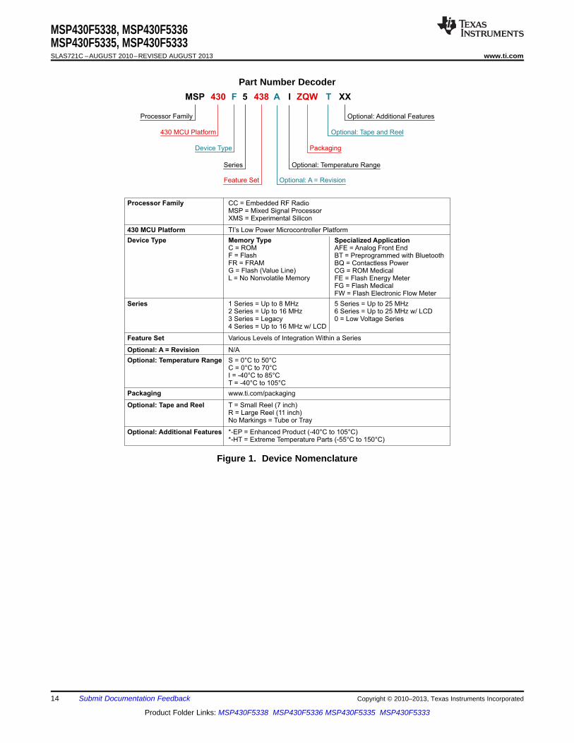
Processor Family CC = Embedded RF RadioMSP = Mixed Signal ProcessorXMS = Experimental Silicon
430 MCU Platform TI’s Low Power Microcontroller Platform
Device Type Memory TypeC = ROMF = FlashFR = FRAMG = Flash (Value Line)L = No Nonvolatile Memory
Specialized ApplicationAFE = Analog Front EndBT = Preprogrammed with BluetoothBQ = Contactless PowerCG = ROM MedicalFE = Flash Energy MeterFG = Flash MedicalFW = Flash Electronic Flow Meter
Series 1 Series = Up to 8 MHz2 Series = Up to 16 MHz3 Series = Legacy4 Series = Up to 16 MHz w/ LCD
5 Series = Up to 25 MHz6 Series = Up to 25 MHz w/ LCD0 = Low Voltage Series
Feature Set Various Levels of Integration Within a Series
Optional: A = Revision N/A
Optional: Temperature Range S = 0°C to 50 CC to 70 C
I = -40 C to 85 CT = -40 C to 105 C
°C = 0° °
° °° °
Packaging www.ti.com/packaging
Optional: Tape and Reel T = Small Reel (7 inch)R = Large Reel (11 inch)No Markings = Tube or Tray
Optional: Additional Features *-EP = Enhanced Product (-40°C to 105°C)*-HT = Extreme Temperature Parts (-55°C to 150°C)
MSP 430 F 5 438 A I ZQW T XX
Processor Family
Series Optional: Temperature Range
430 MCU Platform
PackagingDevice Type
Optional: A = Revision
Optional: Tape and Reel
Feature Set
Optional: Additional Features
MSP430F5338, MSP430F5336MSP430F5335, MSP430F5333SLAS721C –AUGUST 2010–REVISED AUGUST 2013 www.ti.com
Part Number Decoder
Figure 1. Device Nomenclature
14 Submit Documentation Feedback Copyright © 2010–2013, Texas Instruments Incorporated
Product Folder Links: MSP430F5338 MSP430F5336 MSP430F5335 MSP430F5333
Program Counter PC/R0
Stack Pointer SP/R1
Status Register SR/CG1/R2
Constant Generator CG2/R3
General-Purpose Register R4
General-Purpose Register R5
General-Purpose Register R6
General-Purpose Register R7
General-Purpose Register R8
General-Purpose Register R9
General-Purpose Register R10
General-Purpose Register R11
General-Purpose Register R12
General-Purpose Register R13
General-Purpose Register R15
General-Purpose Register R14
MSP430F5338, MSP430F5336MSP430F5335, MSP430F5333
www.ti.com SLAS721C –AUGUST 2010–REVISED AUGUST 2013
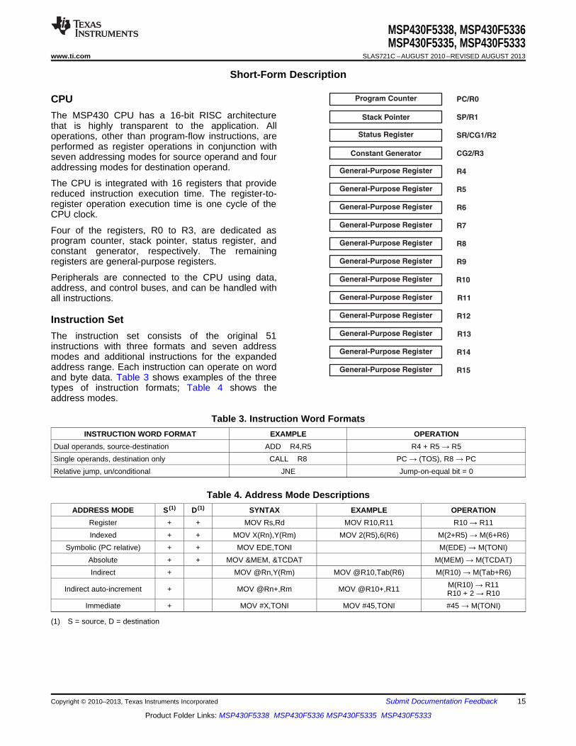
Short-Form Description
CPUThe MSP430 CPU has a 16-bit RISC architecturethat is highly transparent to the application. Alloperations, other than program-flow instructions, areperformed as register operations in conjunction withseven addressing modes for source operand and fouraddressing modes for destination operand.
The CPU is integrated with 16 registers that providereduced instruction execution time. The register-to-register operation execution time is one cycle of theCPU clock.
Four of the registers, R0 to R3, are dedicated asprogram counter, stack pointer, status register, andconstant generator, respectively. The remainingregisters are general-purpose registers.
Peripherals are connected to the CPU using data,address, and control buses, and can be handled withall instructions.
Instruction SetThe instruction set consists of the original 51instructions with three formats and seven addressmodes and additional instructions for the expandedaddress range. Each instruction can operate on wordand byte data. Table 3 shows examples of the threetypes of instruction formats; Table 4 shows theaddress modes.
Table 3. Instruction Word FormatsINSTRUCTION WORD FORMAT EXAMPLE OPERATION
Dual operands, source-destination ADD R4,R5 R4 + R5 → R5Single operands, destination only CALL R8 PC → (TOS), R8 → PCRelative jump, un/conditional JNE Jump-on-equal bit = 0
Table 4. Address Mode DescriptionsADDRESS MODE S (1) D (1) SYNTAX EXAMPLE OPERATION
Register + + MOV Rs,Rd MOV R10,R11 R10 → R11Indexed + + MOV X(Rn),Y(Rm) MOV 2(R5),6(R6) M(2+R5) → M(6+R6)
Symbolic (PC relative) + + MOV EDE,TONI M(EDE) → M(TONI)Absolute + + MOV &MEM, &TCDAT M(MEM) → M(TCDAT)Indirect + MOV @Rn,Y(Rm) MOV @R10,Tab(R6) M(R10) → M(Tab+R6)
M(R10) → R11Indirect auto-increment + MOV @Rn+,Rm MOV @R10+,R11 R10 + 2 → R10Immediate + MOV #X,TONI MOV #45,TONI #45 → M(TONI)
(1) S = source, D = destination
Copyright © 2010–2013, Texas Instruments Incorporated Submit Documentation Feedback 15
Product Folder Links: MSP430F5338 MSP430F5336 MSP430F5335 MSP430F5333
MSP430F5338, MSP430F5336MSP430F5335, MSP430F5333SLAS721C –AUGUST 2010–REVISED AUGUST 2013 www.ti.com
Operating ModesThe MSP430 has one active mode and seven software selectable low-power modes of operation. An interruptevent can wake up the device from any of the low-power modes, service the request, and restore back to thelow-power mode on return from the interrupt program.
The following seven operating modes can be configured by software:• Active mode (AM)
– All clocks are active• Low-power mode 0 (LPM0)
– CPU is disabled– ACLK and SMCLK remain active, MCLK is disabled– FLL loop control remains active
• Low-power mode 1 (LPM1)– CPU is disabled– FLL loop control is disabled– ACLK and SMCLK remain active, MCLK is disabled
• Low-power mode 2 (LPM2)– CPU is disabled– MCLK, FLL loop control, and DCOCLK are disabled– DCO's dc generator remains enabled– ACLK remains active
• Low-power mode 3 (LPM3)– CPU is disabled– MCLK, FLL loop control, and DCOCLK are disabled– DCO's dc generator is disabled– ACLK remains active
• Low-power mode 4 (LPM4)– CPU is disabled– ACLK is disabled– MCLK, FLL loop control, and DCOCLK are disabled– DCO's dc generator is disabled– Crystal oscillator is stopped– Complete data retention
• Low-power mode 3.5 (LPM3.5)– Internal regulator disabled– No data retention– RTC enabled and clocked by low-frequency oscillator– Wakeup from RST/NMI, RTC_B, P1, P2, P3, and P4
• Low-power mode 4.5 (LPM4.5)– Internal regulator disabled– No data retention– Wakeup from RST/NMI, RTC_B, P1, P2, P3, and P4
16 Submit Documentation Feedback Copyright © 2010–2013, Texas Instruments Incorporated
Product Folder Links: MSP430F5338 MSP430F5336 MSP430F5335 MSP430F5333
MSP430F5338, MSP430F5336MSP430F5335, MSP430F5333
www.ti.com SLAS721C –AUGUST 2010–REVISED AUGUST 2013
Interrupt Vector AddressesThe interrupt vectors and the power-up start address are located in the address range 0FFFFh to 0FF80h. Thevector contains the 16-bit address of the appropriate interrupt-handler instruction sequence.
Table 5. Interrupt Sources, Flags, and Vectors of MSP430F533x ConfigurationsSYSTEM WORDINTERRUPT SOURCE INTERRUPT FLAG PRIORITYINTERRUPT ADDRESS
System ResetPower-Up, External Reset WDTIFG, KEYV (SYSRSTIV) (1) (2) Reset 0FFFEh 63, highestWatchdog Timeout, Key Violation
Flash Memory Key ViolationSystem NMI SVMLIFG, SVMHIFG, DLYLIFG, DLYHIFG,PMM VLRLIFG, VLRHIFG, VMAIFG, JMBNIFG, (Non)maskable 0FFFCh 62Vacant Memory Access JMBOUTIFG (SYSSNIV) (1)
JTAG MailboxUser NMI
NMI NMIIFG, OFIFG, ACCVIFG, BUSIFG (Non)maskable 0FFFAh 61Oscillator Fault (SYSUNIV) (1) (2)
Flash Memory Access ViolationComp_B Comparator B interrupt flags (CBIV) (1) (3) Maskable 0FFF8h 60
Timer TB0 TB0CCR0 CCIFG0 (3) Maskable 0FFF6h 59TB0CCR1 CCIFG1 to TB0CCR6 CCIFG6,Timer TB0 Maskable 0FFF4h 58TB0IFG (TBIV) (1) (3)
Watchdog Interval Timer Mode WDTIFG Maskable 0FFF2h 57USCI_A0 Receive or Transmit UCA0RXIFG, UCA0TXIFG (UCA0IV) (1) (3) Maskable 0FFF0h 56USCI_B0 Receive or Transmit UCB0RXIFG, UCB0TXIFG (UCB0IV) (1) (3) Maskable 0FFEEh 55
ADC12_A ADC12IFG0 to ADC12IFG15 (ADC12IV) (1) (3) Maskable 0FFECh 54Timer TA0 TA0CCR0 CCIFG0 (3) Maskable 0FFEAh 53
TA0CCR1 CCIFG1 to TA0CCR4 CCIFG4,Timer TA0 Maskable 0FFE8h 52TA0IFG (TA0IV) (1) (3)
LDO-PWR LDOOFFIG, LDOONIFG, LDOOVLIFG Maskable 0FFE6h 51DMA0IFG, DMA1IFG, DMA2IFG, DMA3IFG,DMA Maskable 0FFE4h 50DMA4IFG, DMA5IFG (DMAIV) (1) (3)
Timer TA1 TA1CCR0 CCIFG0 (3) Maskable 0FFE2h 49TA1CCR1 CCIFG1 to TA1CCR2 CCIFG2,Timer TA1 Maskable 0FFE0h 48TA1IFG (TA1IV) (1) (3)
I/O Port P1 P1IFG.0 to P1IFG.7 (P1IV) (1) (3) Maskable 0FFDEh 47USCI_A1 Receive or Transmit UCA1RXIFG, UCA1TXIFG (UCA1IV) (1) (3) Maskable 0FFDCh 46USCI_B1 Receive or Transmit UCB1RXIFG, UCB1TXIFG (UCB1IV) (1) (3) Maskable 0FFDAh 45
I/O Port P2 P2IFG.0 to P2IFG.7 (P2IV) (1) (3) Maskable 0FFD8h 44Reserved Reserved Maskable 0FFD6h 43
RTCRDYIFG, RTCTEVIFG, RTCAIFG,RTC_B Maskable 0FFD4h 42RT0PSIFG, RT1PSIFG, RTCOFIFG (RTCIV) (1) (3)
DAC12_A (4) DAC12_0IFG, DAC12_1IFG (1) (3) Maskable 0FFD2h 41Timer TA2 TA2CCR0 CCIFG0 (3) Maskable 0FFD0h 40
TA2CCR1 CCIFG1 to TA2CCR2 CCIFG2,Timer TA2 Maskable 0FFCEh 39TA2IFG (TA2IV) (1) (3)
I/O Port P3 P3IFG.0 to P3IFG.7 (P3IV) (1) (3) Maskable 0FFCCh 38I/O Port P4 P4IFG.0 to P4IFG.7 (P4IV) (1) (3) Maskable 0FFCAh 37
(1) Multiple source flags(2) A reset is generated if the CPU tries to fetch instructions from within peripheral space or vacant memory space.
(Non)maskable: the individual interrupt-enable bit can disable an interrupt event, but the general-interrupt enable cannot disable it.(3) Interrupt flags are located in the module.(4) Only on devices with peripheral module DAC12_A, otherwise reserved.
Copyright © 2010–2013, Texas Instruments Incorporated Submit Documentation Feedback 17
Product Folder Links: MSP430F5338 MSP430F5336 MSP430F5335 MSP430F5333
MSP430F5338, MSP430F5336MSP430F5335, MSP430F5333SLAS721C –AUGUST 2010–REVISED AUGUST 2013 www.ti.com
Table 5. Interrupt Sources, Flags, and Vectors of MSP430F533x Configurations (continued)SYSTEM WORDINTERRUPT SOURCE INTERRUPT FLAG PRIORITYINTERRUPT ADDRESS
0FFC8h 36Reserved Reserved (5) ⋮ ⋮
0FF80h 0, lowest
(5) Reserved interrupt vectors at addresses are not used in this device and can be used for regular program code if necessary. To maintaincompatability with other devices, it is recommended to reserve these locations.
Memory Organization
Table 6. Memory Organization (1) (2)
MSP430F5338MSP430F5333 MSP430F5336 MSP430F5335Memory (flash) Total Size 128KB 128KB 256KBMain: interrupt vector 00FFFFh–00FF80h 00FFFFh–00FF80h 00FFFFh–00FF80h
Bank 3 N/A N/A 64 KB047FFF-038000h
Bank 2 N/A N/A 64 KB037FFF-028000h
Main: code memoryBank 1 64 KB 64 KB 64 KB
027FFF-018000h 027FFF-018000h 027FFF-018000hBank 0 64 KB 64 KB 64 KB
017FFF-008000h 017FFF-008000h 017FFF-008000hSector 3 N/A 4 KB 4 KB
0063FFh–005400h 0063FFh–005400hSector 2 N/A 4 KB 4 KB
0053FFh–004400h 0053FFh–004400hRAM
Sector 1 4 KB 4 KB 4 KB0043FFh–003400h 0043FFh–003400h 0043FFh–003400h
Sector 0 4 KB 4 KB 4 KB0033FFh–002400h 0033FFh–002400h 0033FFh–002400h
Sector 7 2KB 2KB 2KBRAM 0023FFh-001C00h 0023FFh-001C00h 0023FFh-001C00hInfo A 128 B 128 B 128 B
0019FFh–001980h 0019FFh–001980h 0019FFh–001980hInfo B 128 B 128 B 128 B
00197Fh–001900h 00197Fh–001900h 00197Fh–001900hInformation memory(flash) Info C 128 B 128 B 128 B
0018FFh–001880h 0018FFh–001880h 0018FFh–001880hInfo D 128 B 128 B 128 B
00187Fh–001800h 00187Fh–001800h 00187Fh–001800hBSL 3 512 B 512 B 512 B
0017FFh–001600h 0017FFh–001600h 0017FFh–001600hBSL 2 512 B 512 B 512 B
0015FFh–001400h 0015FFh–001400h 0015FFh–001400hBootstrap loader (BSL)memory (flash) BSL 1 512 B 512 B 512 B
0013FFh–001200h 0013FFh–001200h 0013FFh–001200hBSL 0 512 B 512 B 512 B
0011FFh–001000h 0011FFh–001000h 0011FFh–001000hSize 4KB 4KB 4KBPeripherals 000FFFh–000000h 000FFFh–000000h 000FFFh–000000h
(1) N/A = Not available.(2) Backup RAM is accessed via the control registers BAKMEM0, BAKMEM1, BAKMEM2, and BAKMEM3.
18 Submit Documentation Feedback Copyright © 2010–2013, Texas Instruments Incorporated
Product Folder Links: MSP430F5338 MSP430F5336 MSP430F5335 MSP430F5333
MSP430F5338, MSP430F5336MSP430F5335, MSP430F5333
www.ti.com SLAS721C –AUGUST 2010–REVISED AUGUST 2013
Bootstrap Loader (BSL)The BSL enables users to program the flash memory or RAM using a UART serial interfaces. Access to thedevice memory via the BSL is protected by an user-defined password. Use of the BSL requires external accessto the six pins shown in Table 7. BSL entry requires a specific entry sequence on the RST/NMI/SBWTDIO andTEST/SBWTCK pins. For complete description of the features of the BSL and its implementation, see MSP430Programming Via the Bootstrap Loader (BSL) (SLAU319).
Table 7. UART BSL Pin Requirements and FunctionsDEVICE SIGNAL BSL FUNCTION
RST/NMI/SBWTDIO Entry sequence signalTEST/SBWTCK Entry sequence signal
P1.1 Data transmitP1.2 Data receiveVCC Power supplyVSS Ground supply
JTAG Operation
JTAG Standard InterfaceThe MSP430 family supports the standard JTAG interface which requires four signals for sending and receivingdata. The JTAG signals are shared with general-purpose I/O. The TEST/SBWTCK pin is used to enable theJTAG signals. In addition to these signals, the RST/NMI/SBWTDIO is required to interface with MSP430development tools and device programmers. The JTAG pin requirements are shown in Table 8. For furtherdetails on interfacing to development tools and device programmers, see the MSP430(tm) Hardware ToolsUser's Guide (SLAU278). For a complete description of the features of the JTAG interface and itsimplementation, see MSP430 Programming Via the JTAG Interface (SLAU320).
Table 8. JTAG Pin Requirements and FunctionsDEVICE SIGNAL DIRECTION FUNCTION
PJ.3/TCK IN JTAG clock inputPJ.2/TMS IN JTAG state control
PJ.1/TDI/TCLK IN JTAG data input, TCLK inputPJ.0/TDO OUT JTAG data output
TEST/SBWTCK IN Enable JTAG pinsRST/NMI/SBWTDIO IN External reset
VCC Power supplyVSS Ground supply
Spy-Bi-Wire InterfaceIn addition to the standard JTAG interface, the MSP430 family supports the two wire Spy-Bi-Wire interface. Spy-Bi-Wire can be used to interface with MSP430 development tools and device programmers. The Spy-Bi-Wireinterface pin requirements are shown in Table 9. For further details on interfacing to development tools anddevice programmers, see the MSP430(tm) Hardware Tools User's Guide (SLAU278). For a complete descriptionof the features of the JTAG interface and its implementation, see MSP430 Programming Via the JTAG Interface(SLAU320).
Table 9. Spy-Bi-Wire Pin Requirements and FunctionsDEVICE SIGNAL DIRECTION FUNCTIONTEST/SBWTCK IN Spy-Bi-Wire clock input
RST/NMI/SBWTDIO IN, OUT Spy-Bi-Wire data input/outputVCC Power supply
Copyright © 2010–2013, Texas Instruments Incorporated Submit Documentation Feedback 19
Product Folder Links: MSP430F5338 MSP430F5336 MSP430F5335 MSP430F5333
MSP430F5338, MSP430F5336MSP430F5335, MSP430F5333SLAS721C –AUGUST 2010–REVISED AUGUST 2013 www.ti.com
Table 9. Spy-Bi-Wire Pin Requirements and Functions (continued)DEVICE SIGNAL DIRECTION FUNCTION
VSS Ground supply
Flash Memory (Link to User's Guide)The flash memory can be programmed via the JTAG port, Spy-Bi-Wire (SBW), the BSL, or in-system by theCPU. The CPU can perform single-byte, single-word, and long-word writes to the flash memory. Features of theflash memory include:• Flash memory has n segments of main memory and four segments of information memory (A to D) of
128 bytes each. Each segment in main memory is 512 bytes in size.• Segments 0 to n may be erased in one step, or each segment may be individually erased.• Segments A to D can be erased individually, or as a group with segments 0 to n. Segments A to D are also
called information memory.• Segment A can be locked separately.
RAM Memory (Link to User's Guide)The RAM memory is made up of n sectors. Each sector can be completely powered down to save leakage,however all data is lost. Features of the RAM memory include:• RAM memory has n sectors. The size of a sector can be found in Memory Organization.• Each sector 0 to n can be complete disabled, however data retention is lost.• Each sector 0 to n automatically enters low power retention mode when possible.
Backup RAM MemoryThe backup RAM provides a limited number of bytes of RAM that are retained during LPMx.5 and duringoperation from a backup supply if the Battery Backup System module is implemented.
There are 8 bytes of Backup RAM available on MSP430F533x. It can be wordwise accessed via the controlregisters BAKMEM0, BAKMEM1, BAKMEM2, and BAKMEM3.
PeripheralsPeripherals are connected to the CPU through data, address, and control buses and can be handled using allinstructions. For complete module descriptions, see the MSP430x5xx and MSP430x6xx Family User's Guide(SLAU208).
Digital I/O (Link to User's Guide)There are up to nine 8-bit I/O ports implemented: P1 through P6, P8, and P9 are complete, P7 contains sixindividual I/O ports, and PJ contains four individual I/O ports.• All individual I/O bits are independently programmable.• Any combination of input, output, and interrupt conditions is possible.• Programmable pullup or pulldown on all ports.• Programmable drive strength on all ports.• Edge-selectable interrupt input capability for all the eight bits of ports P1, P2, P3, and P4.• Read/write access to port-control registers is supported by all instructions.• Ports can be accessed byte-wise (P1 through P9) or word-wise in pairs (PA through PD).
Port Mapping Controller (Link to User's Guide)The port mapping controller allows the flexible and reconfigurable mapping of digital functions to port P2.
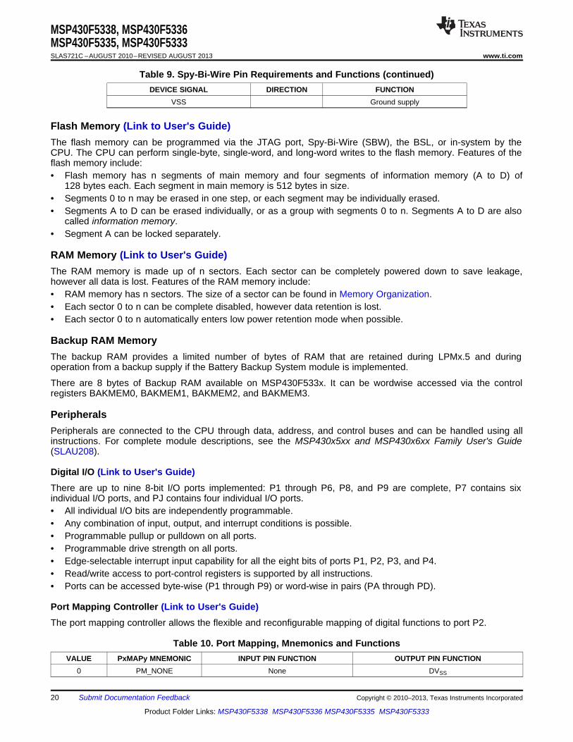
Table 10. Port Mapping, Mnemonics and FunctionsVALUE PxMAPy MNEMONIC INPUT PIN FUNCTION OUTPUT PIN FUNCTION
0 PM_NONE None DVSS
20 Submit Documentation Feedback Copyright © 2010–2013, Texas Instruments Incorporated
Product Folder Links: MSP430F5338 MSP430F5336 MSP430F5335 MSP430F5333
MSP430F5338, MSP430F5336MSP430F5335, MSP430F5333
www.ti.com SLAS721C –AUGUST 2010–REVISED AUGUST 2013
Table 10. Port Mapping, Mnemonics and Functions (continued)VALUE PxMAPy MNEMONIC INPUT PIN FUNCTION OUTPUT PIN FUNCTION
PM_CBOUT - Comparator_B output1
PM_TB0CLK Timer TB0 clock input -PM_ADC12CLK - ADC12CLK
2PM_DMAE0 DMAE0 Input -
PM_SVMOUT - SVM output3 Timer TB0 high impedance inputPM_TB0OUTH -TB0OUTH4 PM_TB0CCR0B Timer TB0 CCR0 capture input CCI0B Timer TB0: TB0.0 compare output Out05 PM_TB0CCR1B Timer TB0 CCR1 capture input CCI1B Timer TB0: TB0.1 compare output Out16 PM_TB0CCR2B Timer TB0 CCR2 capture input CCI2B Timer TB0: TB0.2 compare output Out27 PM_TB0CCR3B Timer TB0 CCR3 capture input CCI3B Timer TB0: TB0.3 compare output Out38 PM_TB0CCR4B Timer TB0 CCR4 capture input CCI4B Timer TB0: TB0.4 compare output Out49 PM_TB0CCR5B Timer TB0 CCR5 capture input CCI5B Timer TB0: TB0.5 compare output Out5
10 PM_TB0CCR6B Timer TB0 CCR6 capture input CCI6B Timer TB0: TB0.6 compare output Out6PM_UCA0RXD USCI_A0 UART RXD (Direction controlled by USCI - input)
11PM_UCA0SOMI USCI_A0 SPI slave out master in (direction controlled by USCI)PM_UCA0TXD USCI_A0 UART TXD (Direction controlled by USCI - output)
12PM_UCA0SIMO USCI_A0 SPI slave in master out (direction controlled by USCI)PM_UCA0CLK USCI_A0 clock input/output (direction controlled by USCI)
13PM_UCB0STE USCI_B0 SPI slave transmit enable (direction controlled by USCI - input)
PM_UCB0SOMI USCI_B0 SPI slave out master in (direction controlled by USCI)14
PM_UCB0SCL USCI_B0 I2C clock (open drain and direction controlled by USCI)PM_UCB0SIMO USCI_B0 SPI slave in master out (direction controlled by USCI)
15PM_UCB0SDA USCI_B0 I2C data (open drain and direction controlled by USCI)PM_UCB0CLK USCI_B0 clock input/output (direction controlled by USCI)
16PM_UCA0STE USCI_A0 SPI slave transmit enable (direction controlled by USCI - input)
17 PM_MCLK - MCLK18 Reserved Reserved for test purposes. Do not use this setting.19 Reserved Reserved for test purposes. Do not use this setting.
20-30 Reserved None DVSSDisables the output driver and the input Schmitt-trigger to prevent parasitic cross currents31 (0FFh) (1) PM_ANALOG when applying analog signals.
(1) The value of the PM_ANALOG mnemonic is set to 0FFh. The port mapping registers are only 5 bits wide and the upper bits are ignored,which results in a read out value of 31.
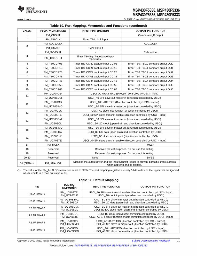
Table 11. Default MappingPxMAPyPIN INPUT PIN FUNCTION OUTPUT PIN FUNCTIONMNEMONIC
PM_UCB0STE, USCI_B0 SPI slave transmit enable (direction controlled by USCI - input),P2.0/P2MAP0 PM_UCA0CLK USCI_A0 clock input/output (direction controlled by USCI)PM_UCB0SIMO, USCI_B0 SPI slave in master out (direction controlled by USCI),P2.1/P2MAP1 PM_UCB0SDA USCI_B0 I2C data (open drain and direction controlled by USCI)PM_UCB0SOMI, USCI_B0 SPI slave out master in (direction controlled by USCI),P2.2/P2MAP2 PM_UCB0SCL USCI_B0 I2C clock (open drain and direction controlled by USCI)PM_UCB0CLK, USCI_B0 clock input/output (direction controlled by USCI),P2.3/P2MAP3 PM_UCA0STE USCI_A0 SPI slave transmit enable (direction controlled by USCI - input)PM_UCA0TXD, USCI_A0 UART TXD (direction controlled by USCI - output),P2.4/P2MAP4 PM_UCA0SIMO USCI_A0 SPI slave in master out (direction controlled by USCI)PM_UCA0RXD, USCI_A0 UART RXD (direction controlled by USCI - input),P2.5/P2MAP5 PM_UCA0SOMI USCI_A0 SPI slave out master in (direction controlled by USCI)
Copyright © 2010–2013, Texas Instruments Incorporated Submit Documentation Feedback 21
Product Folder Links: MSP430F5338 MSP430F5336 MSP430F5335 MSP430F5333
MSP430F5338, MSP430F5336MSP430F5335, MSP430F5333SLAS721C –AUGUST 2010–REVISED AUGUST 2013 www.ti.com
Table 11. Default Mapping (continued)PxMAPyPIN INPUT PIN FUNCTION OUTPUT PIN FUNCTIONMNEMONIC
P2.6/P2MAP6 PM_NONE - DVSSP2.7/P2MAP7 PM_NONE - DVSS
Oscillator and System Clock (Link to User's Guide)The clock system in the MSP430F533x family of devices is supported by the Unified Clock System (UCS)module that includes support for a 32-kHz watch crystal oscillator (in XT1 LF mode; XT1 HF mode is notsupported), an internal very-low-power low-frequency oscillator (VLO), an internal trimmed low-frequencyoscillator (REFO), an integrated internal digitally controlled oscillator (DCO), and a high-frequency crystaloscillator XT2. The UCS module is designed to meet the requirements of both low system cost and low powerconsumption. The UCS module features digital frequency locked loop (FLL) hardware that, in conjunction with adigital modulator, stabilizes the DCO frequency to a programmable multiple of the watch crystal frequency. Theinternal DCO provides a fast turn-on clock source and stabilizes in 3 µs (typical). The UCS module provides thefollowing clock signals:• Auxiliary clock (ACLK), sourced from a 32-kHz watch crystal (XT1), a high-frequency crystal (XT2), the
internal low-frequency oscillator (VLO), the trimmed low-frequency oscillator (REFO), or the internal digitally-controlled oscillator DCO.
• Main clock (MCLK), the system clock used by the CPU. MCLK can be sourced by same sources available toACLK.
• Sub-Main clock (SMCLK), the subsystem clock used by the peripheral modules. SMCLK can be sourced bysame sources available to ACLK.
• ACLK/n, the buffered output of ACLK, ACLK/2, ACLK/4, ACLK/8, ACLK/16, ACLK/32.
Power Management Module (PMM) (Link to User's Guide)The PMM includes an integrated voltage regulator that supplies the core voltage to the device and containsprogrammable output levels to provide for power optimization. The PMM also includes supply voltage supervisor(SVS) and supply voltage monitoring (SVM) circuitry, as well as brownout protection. The brownout circuit isimplemented to provide the proper internal reset signal to the device during power-on and power-off. The SVSand SVM circuitry detects if the supply voltage drops below a user-selectable level and supports both supplyvoltage supervision (the device is automatically reset) and supply voltage monitoring (the device is notautomatically reset). SVS and SVM circuitry is available on the primary supply and core supply.
Hardware Multiplier (MPY) (Link to User's Guide)The multiplication operation is supported by a dedicated peripheral module. The module performs operations with32-bit, 24-bit, 16-bit, and 8-bit operands. The module is capable of supporting signed and unsigned multiplicationas well as signed and unsigned multiply and accumulate operations.
Real-Time Clock (RTC_B) (Link to User's Guide)The RTC_B module can be configured for real-time clock (RTC) or calendar mode providing seconds, minutes,hours, day of week, day of month, month, and year. Calendar mode integrates an internal calendar whichcompensates for months with less than 31 days and includes leap year correction. The RTC_B also supportsflexible alarm functions and offset-calibration hardware. The implementation on this device supports operation inLPM3.5 mode and operation from a backup supply.
Watchdog Timer (WDT_A) (Link to User's Guide)The primary function of the watchdog timer (WDT_A) module is to perform a controlled system restart after asoftware problem occurs. If the selected time interval expires, a system reset is generated. If the watchdogfunction is not needed in an application, the module can be configured as an interval timer and can generateinterrupts at selected time intervals.
22 Submit Documentation Feedback Copyright © 2010–2013, Texas Instruments Incorporated
Product Folder Links: MSP430F5338 MSP430F5336 MSP430F5335 MSP430F5333
MSP430F5338, MSP430F5336MSP430F5335, MSP430F5333
www.ti.com SLAS721C –AUGUST 2010–REVISED AUGUST 2013
System Module (SYS) (Link to User's Guide)The SYS module handles many of the system functions within the device. These include power-on reset andpower-up clear handling, NMI source selection and management, reset interrupt vector generators, bootstraploader entry mechanisms, and configuration management (device descriptors). SYS also includes a dataexchange mechanism via JTAG called a JTAG mailbox that can be used in the application.
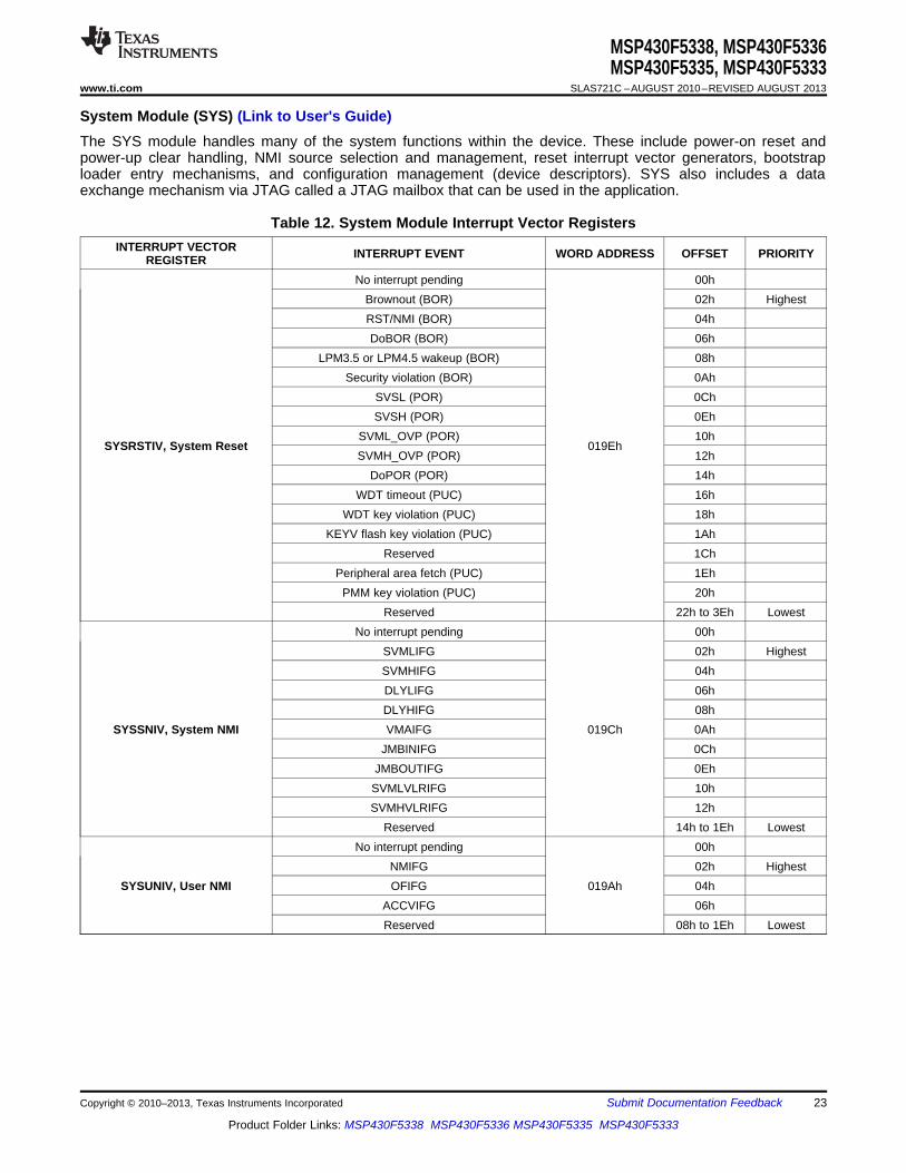
Table 12. System Module Interrupt Vector RegistersINTERRUPT VECTOR INTERRUPT EVENT WORD ADDRESS OFFSET PRIORITYREGISTER
No interrupt pending 00hBrownout (BOR) 02h HighestRST/NMI (BOR) 04hDoBOR (BOR) 06h
LPM3.5 or LPM4.5 wakeup (BOR) 08hSecurity violation (BOR) 0Ah
SVSL (POR) 0ChSVSH (POR) 0Eh
SVML_OVP (POR) 10hSYSRSTIV, System Reset 019Eh
SVMH_OVP (POR) 12hDoPOR (POR) 14h
WDT timeout (PUC) 16hWDT key violation (PUC) 18h
KEYV flash key violation (PUC) 1AhReserved 1Ch
Peripheral area fetch (PUC) 1EhPMM key violation (PUC) 20h
Reserved 22h to 3Eh LowestNo interrupt pending 00h
SVMLIFG 02h HighestSVMHIFG 04hDLYLIFG 06hDLYHIFG 08h
SYSSNIV, System NMI VMAIFG 019Ch 0AhJMBINIFG 0Ch
JMBOUTIFG 0EhSVMLVLRIFG 10hSVMHVLRIFG 12h
Reserved 14h to 1Eh LowestNo interrupt pending 00h
NMIFG 02h HighestSYSUNIV, User NMI OFIFG 019Ah 04h
ACCVIFG 06hReserved 08h to 1Eh Lowest
Copyright © 2010–2013, Texas Instruments Incorporated Submit Documentation Feedback 23
Product Folder Links: MSP430F5338 MSP430F5336 MSP430F5335 MSP430F5333
MSP430F5338, MSP430F5336MSP430F5335, MSP430F5333SLAS721C –AUGUST 2010–REVISED AUGUST 2013 www.ti.com
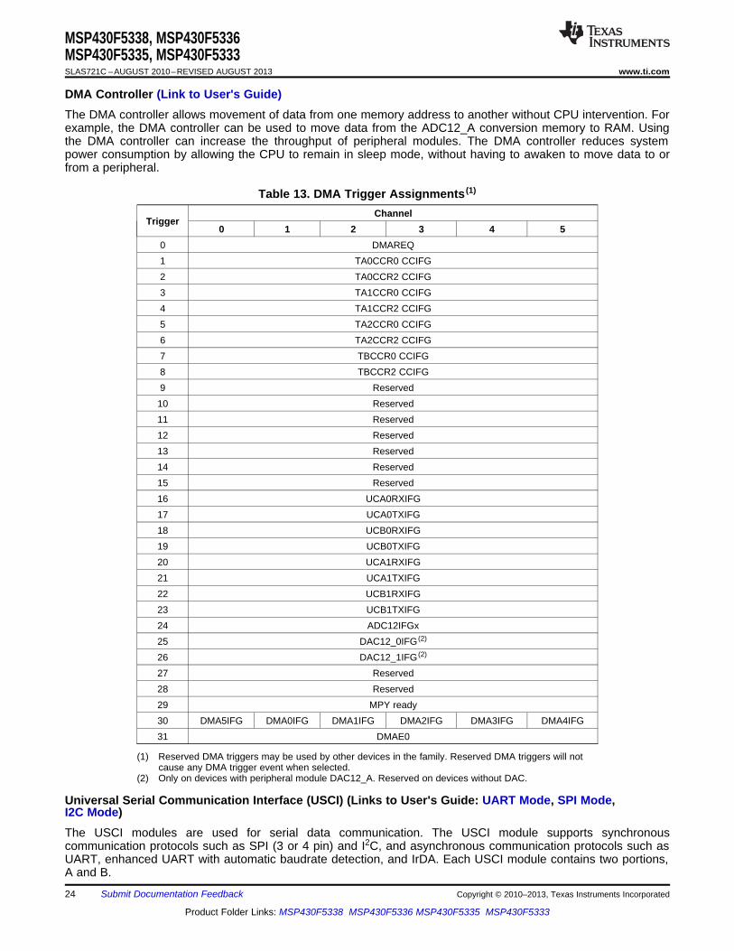
DMA Controller (Link to User's Guide)The DMA controller allows movement of data from one memory address to another without CPU intervention. Forexample, the DMA controller can be used to move data from the ADC12_A conversion memory to RAM. Usingthe DMA controller can increase the throughput of peripheral modules. The DMA controller reduces systempower consumption by allowing the CPU to remain in sleep mode, without having to awaken to move data to orfrom a peripheral.
Table 13. DMA Trigger Assignments (1)
ChannelTrigger
0 1 2 3 4 50 DMAREQ1 TA0CCR0 CCIFG2 TA0CCR2 CCIFG3 TA1CCR0 CCIFG4 TA1CCR2 CCIFG5 TA2CCR0 CCIFG6 TA2CCR2 CCIFG7 TBCCR0 CCIFG8 TBCCR2 CCIFG9 Reserved10 Reserved11 Reserved12 Reserved13 Reserved14 Reserved15 Reserved16 UCA0RXIFG17 UCA0TXIFG18 UCB0RXIFG19 UCB0TXIFG20 UCA1RXIFG21 UCA1TXIFG22 UCB1RXIFG23 UCB1TXIFG24 ADC12IFGx25 DAC12_0IFG (2)
26 DAC12_1IFG (2)
27 Reserved28 Reserved29 MPY ready30 DMA5IFG DMA0IFG DMA1IFG DMA2IFG DMA3IFG DMA4IFG31 DMAE0
(1) Reserved DMA triggers may be used by other devices in the family. Reserved DMA triggers will notcause any DMA trigger event when selected.
(2) Only on devices with peripheral module DAC12_A. Reserved on devices without DAC.
Universal Serial Communication Interface (USCI) (Links to User's Guide: UART Mode, SPI Mode,I2C Mode)The USCI modules are used for serial data communication. The USCI module supports synchronouscommunication protocols such as SPI (3 or 4 pin) and I2C, and asynchronous communication protocols such asUART, enhanced UART with automatic baudrate detection, and IrDA. Each USCI module contains two portions,A and B.
24 Submit Documentation Feedback Copyright © 2010–2013, Texas Instruments Incorporated
Product Folder Links: MSP430F5338 MSP430F5336 MSP430F5335 MSP430F5333
MSP430F5338, MSP430F5336MSP430F5335, MSP430F5333
www.ti.com SLAS721C –AUGUST 2010–REVISED AUGUST 2013
The USCI_An module provides support for SPI (3 or 4 pin), UART, enhanced UART, or IrDA.
The USCI_Bn module provides support for SPI (3 or 4 pin) or I2C.
The MSP430F533x series includes two complete USCI modules (n = 0 to 1).
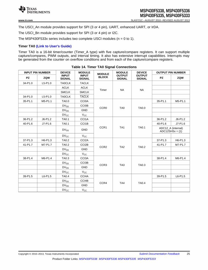
Timer TA0 (Link to User's Guide)Timer TA0 is a 16-bit timer/counter (Timer_A type) with five capture/compare registers. It can support multiplecapture/compares, PWM outputs, and interval timing. It also has extensive interrupt capabilities. Interrupts maybe generated from the counter on overflow conditions and from each of the capture/compare registers.
Table 14. Timer TA0 Signal ConnectionsINPUT PIN NUMBER DEVICE MODULE MODULE DEVICE OUTPUT PIN NUMBERMODULEINPUT INPUT OUTPUT OUTPUTBLOCKPZ ZQW PZ ZQWSIGNAL SIGNAL SIGNAL SIGNAL
34-P1.0 L5-P1.0 TA0CLK TACLKACLK ACLK
Timer NA NASMCLK SMCLK
34-P1.0 L5-P1.0 TA0CLK TACLK35-P1.1 M5-P1.1 TA0.0 CCI0A 35-P1.1 M5-P1.1
DVSS CCI0BCCR0 TA0 TA0.0
DVSS GNDDVCC VCC
36-P1.2 J6-P1.2 TA0.1 CCI1A 36-P1.2 J6-P1.240-P1.6 J7-P1.6 TA0.1 CCI1B 40-P1.6 J7-P1.6
CCR1 TA1 TA0.1 ADC12_A (internal)DVSS GND ADC12SHSx = 1DVCC VCC
37-P1.3 H6-P1.3 TA0.2 CCI2A 37-P1.3 H6-P1.341-P1.7 M7-P1.7 TA0.2 CCI2B 41-P1.7 M7-P1.7
CCR2 TA2 TA0.2DVSS GNDDVCC VCC
38-P1.4 M6-P1.4 TA0.3 CCI3A 38-P1.4 M6-P1.4DVSS CCI3B
CCR3 TA3 TA0.3DVSS GNDDVCC VCC
39-P1.5 L6-P1.5 TA0.4 CCI4A 39-P1.5 L6-P1.5DVSS CCI4B
CCR4 TA4 TA0.4DVSS GNDDVCC VCC
Copyright © 2010–2013, Texas Instruments Incorporated Submit Documentation Feedback 25
Product Folder Links: MSP430F5338 MSP430F5336 MSP430F5335 MSP430F5333
MSP430F5338, MSP430F5336MSP430F5335, MSP430F5333SLAS721C –AUGUST 2010–REVISED AUGUST 2013 www.ti.com
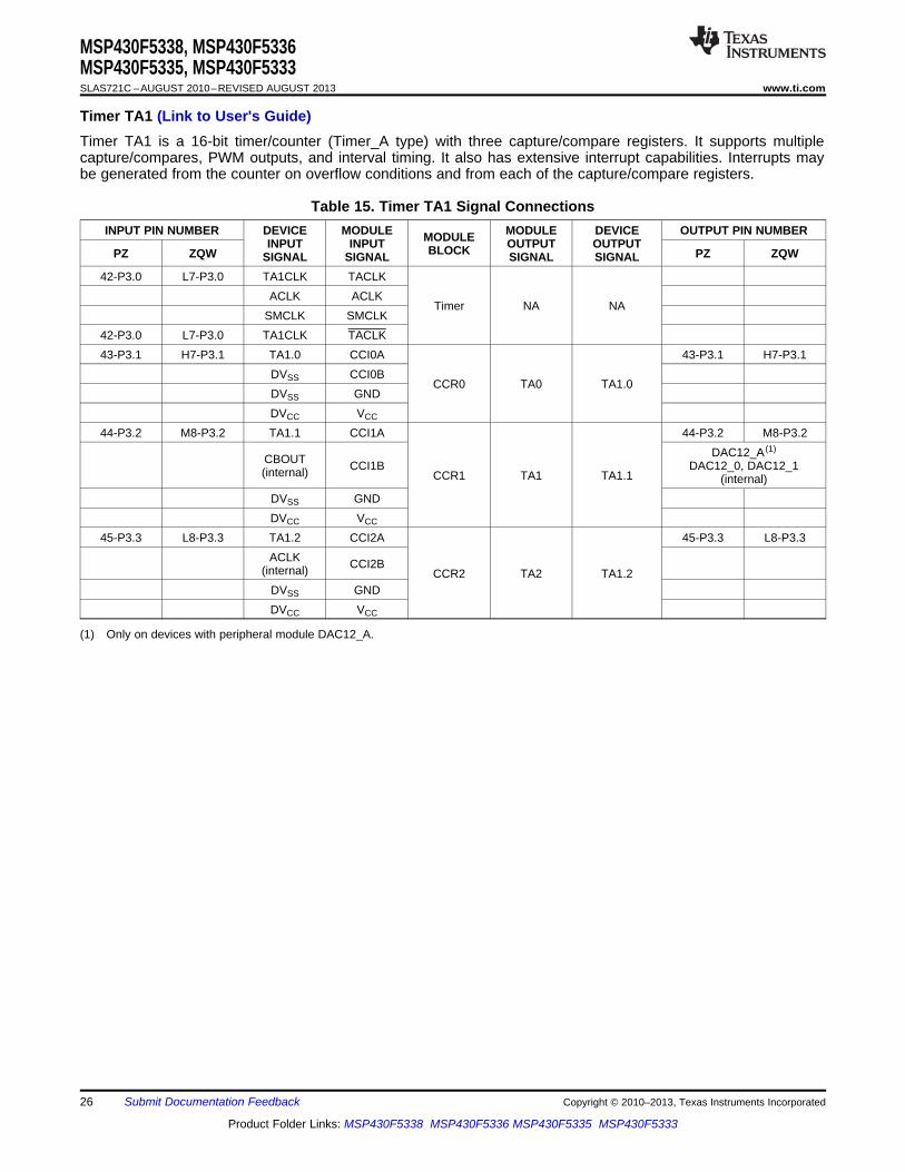
Timer TA1 (Link to User's Guide)Timer TA1 is a 16-bit timer/counter (Timer_A type) with three capture/compare registers. It supports multiplecapture/compares, PWM outputs, and interval timing. It also has extensive interrupt capabilities. Interrupts maybe generated from the counter on overflow conditions and from each of the capture/compare registers.
Table 15. Timer TA1 Signal ConnectionsINPUT PIN NUMBER DEVICE MODULE MODULE DEVICE OUTPUT PIN NUMBERMODULEINPUT INPUT OUTPUT OUTPUTBLOCKPZ ZQW PZ ZQWSIGNAL SIGNAL SIGNAL SIGNAL
42-P3.0 L7-P3.0 TA1CLK TACLKACLK ACLK
Timer NA NASMCLK SMCLK
42-P3.0 L7-P3.0 TA1CLK TACLK43-P3.1 H7-P3.1 TA1.0 CCI0A 43-P3.1 H7-P3.1
DVSS CCI0BCCR0 TA0 TA1.0
DVSS GNDDVCC VCC
44-P3.2 M8-P3.2 TA1.1 CCI1A 44-P3.2 M8-P3.2DAC12_A (1)
CBOUT CCI1B DAC12_0, DAC12_1(internal) CCR1 TA1 TA1.1 (internal)DVSS GNDDVCC VCC
45-P3.3 L8-P3.3 TA1.2 CCI2A 45-P3.3 L8-P3.3ACLK CCI2B(internal) CCR2 TA2 TA1.2DVSS GNDDVCC VCC
(1) Only on devices with peripheral module DAC12_A.
26 Submit Documentation Feedback Copyright © 2010–2013, Texas Instruments Incorporated
Product Folder Links: MSP430F5338 MSP430F5336 MSP430F5335 MSP430F5333
MSP430F5338, MSP430F5336MSP430F5335, MSP430F5333
www.ti.com SLAS721C –AUGUST 2010–REVISED AUGUST 2013
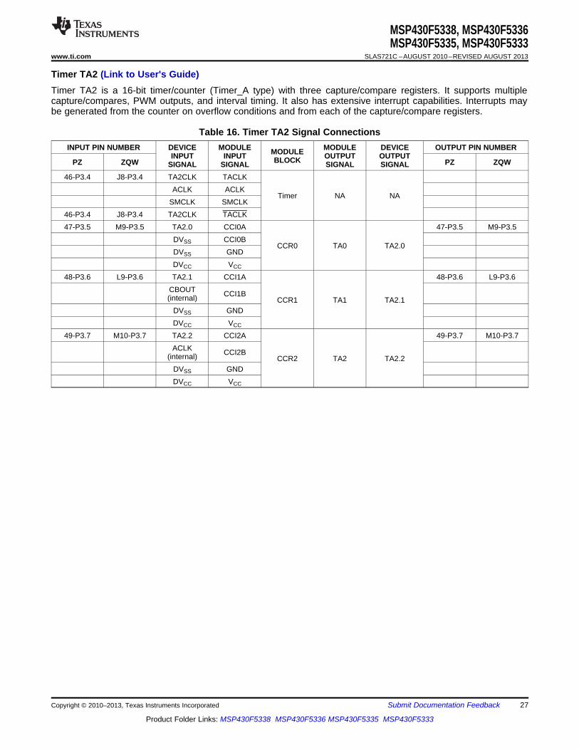
Timer TA2 (Link to User's Guide)Timer TA2 is a 16-bit timer/counter (Timer_A type) with three capture/compare registers. It supports multiplecapture/compares, PWM outputs, and interval timing. It also has extensive interrupt capabilities. Interrupts maybe generated from the counter on overflow conditions and from each of the capture/compare registers.
Table 16. Timer TA2 Signal ConnectionsINPUT PIN NUMBER DEVICE MODULE MODULE DEVICE OUTPUT PIN NUMBERMODULEINPUT INPUT OUTPUT OUTPUTBLOCKPZ ZQW PZ ZQWSIGNAL SIGNAL SIGNAL SIGNAL
46-P3.4 J8-P3.4 TA2CLK TACLKACLK ACLK
Timer NA NASMCLK SMCLK
46-P3.4 J8-P3.4 TA2CLK TACLK47-P3.5 M9-P3.5 TA2.0 CCI0A 47-P3.5 M9-P3.5
DVSS CCI0BCCR0 TA0 TA2.0
DVSS GNDDVCC VCC
48-P3.6 L9-P3.6 TA2.1 CCI1A 48-P3.6 L9-P3.6CBOUT CCI1B(internal) CCR1 TA1 TA2.1DVSS GNDDVCC VCC
49-P3.7 M10-P3.7 TA2.2 CCI2A 49-P3.7 M10-P3.7ACLK CCI2B(internal) CCR2 TA2 TA2.2DVSS GNDDVCC VCC
Copyright © 2010–2013, Texas Instruments Incorporated Submit Documentation Feedback 27
Product Folder Links: MSP430F5338 MSP430F5336 MSP430F5335 MSP430F5333
MSP430F5338, MSP430F5336MSP430F5335, MSP430F5333SLAS721C –AUGUST 2010–REVISED AUGUST 2013 www.ti.com
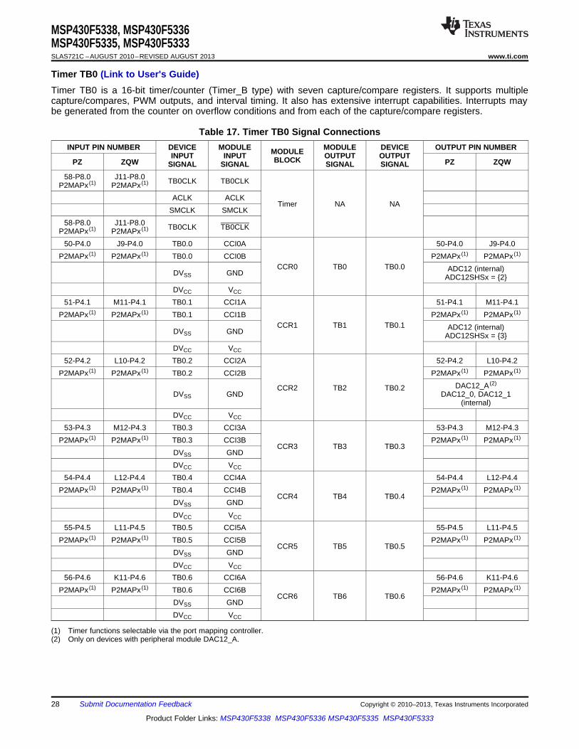
Timer TB0 (Link to User's Guide)Timer TB0 is a 16-bit timer/counter (Timer_B type) with seven capture/compare registers. It supports multiplecapture/compares, PWM outputs, and interval timing. It also has extensive interrupt capabilities. Interrupts maybe generated from the counter on overflow conditions and from each of the capture/compare registers.
Table 17. Timer TB0 Signal ConnectionsINPUT PIN NUMBER DEVICE MODULE MODULE DEVICE OUTPUT PIN NUMBERMODULEINPUT INPUT OUTPUT OUTPUTBLOCKPZ ZQW PZ ZQWSIGNAL SIGNAL SIGNAL SIGNAL
58-P8.0 J11-P8.0 TB0CLK TB0CLKP2MAPx (1) P2MAPx (1)
ACLK ACLKTimer NA NA
SMCLK SMCLK58-P8.0 J11-P8.0 TB0CLK TB0CLKP2MAPx (1) P2MAPx (1)
50-P4.0 J9-P4.0 TB0.0 CCI0A 50-P4.0 J9-P4.0P2MAPx (1) P2MAPx (1) TB0.0 CCI0B P2MAPx (1) P2MAPx (1)
CCR0 TB0 TB0.0 ADC12 (internal)DVSS GND ADC12SHSx = 2DVCC VCC
51-P4.1 M11-P4.1 TB0.1 CCI1A 51-P4.1 M11-P4.1P2MAPx (1) P2MAPx (1) TB0.1 CCI1B P2MAPx (1) P2MAPx (1)
CCR1 TB1 TB0.1 ADC12 (internal)DVSS GND ADC12SHSx = 3DVCC VCC
52-P4.2 L10-P4.2 TB0.2 CCI2A 52-P4.2 L10-P4.2P2MAPx (1) P2MAPx (1) TB0.2 CCI2B P2MAPx (1) P2MAPx (1)
DAC12_A (2)CCR2 TB2 TB0.2
DVSS GND DAC12_0, DAC12_1(internal)
DVCC VCC
53-P4.3 M12-P4.3 TB0.3 CCI3A 53-P4.3 M12-P4.3P2MAPx (1) P2MAPx (1) TB0.3 CCI3B P2MAPx (1) P2MAPx (1)
CCR3 TB3 TB0.3DVSS GNDDVCC VCC
54-P4.4 L12-P4.4 TB0.4 CCI4A 54-P4.4 L12-P4.4P2MAPx (1) P2MAPx (1) TB0.4 CCI4B P2MAPx (1) P2MAPx (1)
CCR4 TB4 TB0.4DVSS GNDDVCC VCC
55-P4.5 L11-P4.5 TB0.5 CCI5A 55-P4.5 L11-P4.5P2MAPx (1) P2MAPx (1) TB0.5 CCI5B P2MAPx (1) P2MAPx (1)
CCR5 TB5 TB0.5DVSS GNDDVCC VCC
56-P4.6 K11-P4.6 TB0.6 CCI6A 56-P4.6 K11-P4.6P2MAPx (1) P2MAPx (1) TB0.6 CCI6B P2MAPx (1) P2MAPx (1)
CCR6 TB6 TB0.6DVSS GNDDVCC VCC
(1) Timer functions selectable via the port mapping controller.(2) Only on devices with peripheral module DAC12_A.
28 Submit Documentation Feedback Copyright © 2010–2013, Texas Instruments Incorporated
Product Folder Links: MSP430F5338 MSP430F5336 MSP430F5335 MSP430F5333
MSP430F5338, MSP430F5336MSP430F5335, MSP430F5333
www.ti.com SLAS721C –AUGUST 2010–REVISED AUGUST 2013
Comparator_B (Link to User's Guide)The primary function of the Comparator_B module is to support precision slope analog-to-digital conversions,battery voltage supervision, and monitoring of external analog signals.
ADC12_A (Link to User's Guide)The ADC12_A module supports fast 12-bit analog-to-digital conversions. The module implements a 12-bit SARcore, sample select control, reference generator, and a 16-word conversion-and-control buffer. The conversion-and-control buffer allows up to 16 independent ADC samples to be converted and stored without any CPUintervention.
DAC12_A (Link to User's Guide)The DAC12_A module is a 12-bit R-ladder voltage-output DAC. The DAC12_A may be used in 8-bit or 12-bitmode, and may be used in conjunction with the DMA controller. When multiple DAC12_A modules are present,they may be grouped together for synchronous operation.
CRC16 (Link to User's Guide)The CRC16 module produces a signature based on a sequence of entered data values and can be used for datachecking purposes. The CRC16 module signature is based on the CRC-CCITT standard.
REF Voltage Reference (Link to User's Guide)The reference module (REF) is responsible for generation of all critical reference voltages that can be used bythe various analog peripherals in the device.
LDO and PU PortThe integrated 3.3-V power system incorporates an integrated 3.3-V LDO regulator that allows the entireMSP430 microcontroller to be powered from nominal 5-V LDOI when it is made available for the system.Alternatively, the power system can supply power only to other components within the system, or it can beunused altogether.
The Port U Pins (PU.0/PU.1) function as general-purpose high-current I/O pins. These pins can only beconfigured together as either both inputs or both outputs. Port U is supplied by the LDOO rail. If the 3.3-V LDO isnot being used in the system (disabled), the LDOO pin can be supplied externally.
Embedded Emulation Module (EEM) (Link to User's Guide)The Embedded Emulation Module (EEM) supports real-time in-system debugging. The L version of the EEMimplemented on these devices has the following features:• Eight hardware triggers or breakpoints on memory access• Two hardware triggers or breakpoints on CPU register write access• Up to ten hardware triggers can be combined to form complex triggers or breakpoints• Two cycle counters• Sequencer• State storage• Clock control on module level
Copyright © 2010–2013, Texas Instruments Incorporated Submit Documentation Feedback 29
Product Folder Links: MSP430F5338 MSP430F5336 MSP430F5335 MSP430F5333
MSP430F5338, MSP430F5336MSP430F5335, MSP430F5333SLAS721C –AUGUST 2010–REVISED AUGUST 2013 www.ti.com
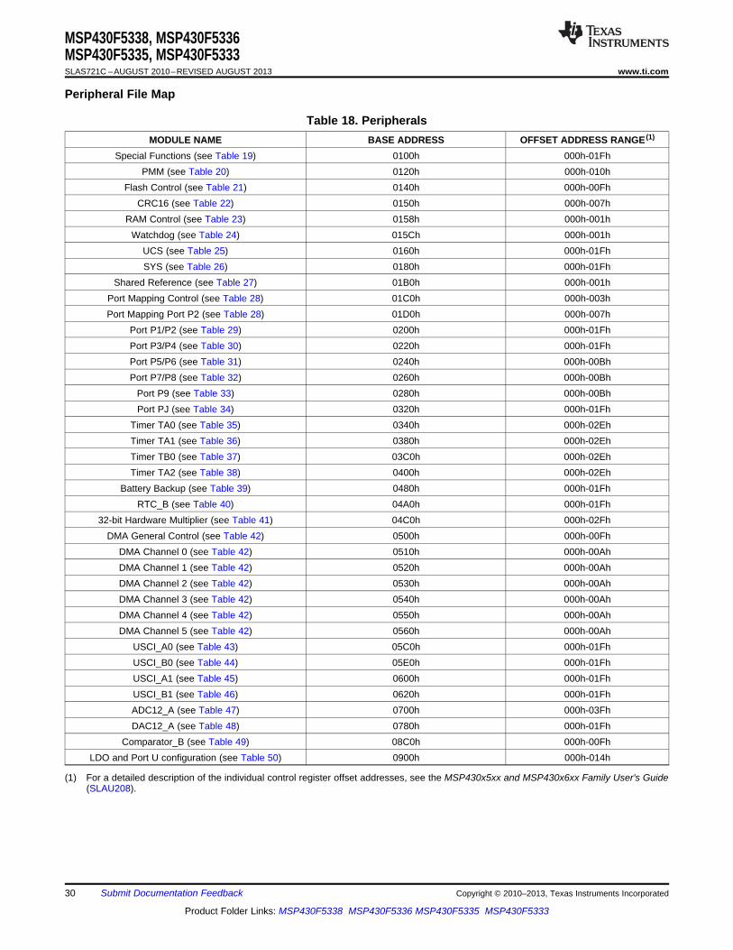
Peripheral File Map
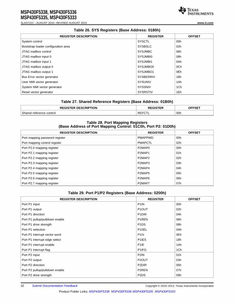
Table 18. PeripheralsMODULE NAME BASE ADDRESS OFFSET ADDRESS RANGE (1)
Special Functions (see Table 19) 0100h 000h-01FhPMM (see Table 20) 0120h 000h-010h
Flash Control (see Table 21) 0140h 000h-00FhCRC16 (see Table 22) 0150h 000h-007h
RAM Control (see Table 23) 0158h 000h-001hWatchdog (see Table 24) 015Ch 000h-001h
UCS (see Table 25) 0160h 000h-01FhSYS (see Table 26) 0180h 000h-01Fh
Shared Reference (see Table 27) 01B0h 000h-001hPort Mapping Control (see Table 28) 01C0h 000h-003hPort Mapping Port P2 (see Table 28) 01D0h 000h-007h
Port P1/P2 (see Table 29) 0200h 000h-01FhPort P3/P4 (see Table 30) 0220h 000h-01FhPort P5/P6 (see Table 31) 0240h 000h-00BhPort P7/P8 (see Table 32) 0260h 000h-00Bh
Port P9 (see Table 33) 0280h 000h-00BhPort PJ (see Table 34) 0320h 000h-01Fh
Timer TA0 (see Table 35) 0340h 000h-02EhTimer TA1 (see Table 36) 0380h 000h-02EhTimer TB0 (see Table 37) 03C0h 000h-02EhTimer TA2 (see Table 38) 0400h 000h-02Eh
Battery Backup (see Table 39) 0480h 000h-01FhRTC_B (see Table 40) 04A0h 000h-01Fh
32-bit Hardware Multiplier (see Table 41) 04C0h 000h-02FhDMA General Control (see Table 42) 0500h 000h-00Fh
DMA Channel 0 (see Table 42) 0510h 000h-00AhDMA Channel 1 (see Table 42) 0520h 000h-00AhDMA Channel 2 (see Table 42) 0530h 000h-00AhDMA Channel 3 (see Table 42) 0540h 000h-00AhDMA Channel 4 (see Table 42) 0550h 000h-00AhDMA Channel 5 (see Table 42) 0560h 000h-00Ah
USCI_A0 (see Table 43) 05C0h 000h-01FhUSCI_B0 (see Table 44) 05E0h 000h-01FhUSCI_A1 (see Table 45) 0600h 000h-01FhUSCI_B1 (see Table 46) 0620h 000h-01FhADC12_A (see Table 47) 0700h 000h-03FhDAC12_A (see Table 48) 0780h 000h-01Fh
Comparator_B (see Table 49) 08C0h 000h-00FhLDO and Port U configuration (see Table 50) 0900h 000h-014h
(1) For a detailed description of the individual control register offset addresses, see the MSP430x5xx and MSP430x6xx Family User's Guide(SLAU208).
30 Submit Documentation Feedback Copyright © 2010–2013, Texas Instruments Incorporated
Product Folder Links: MSP430F5338 MSP430F5336 MSP430F5335 MSP430F5333
MSP430F5338, MSP430F5336MSP430F5335, MSP430F5333
www.ti.com SLAS721C –AUGUST 2010–REVISED AUGUST 2013
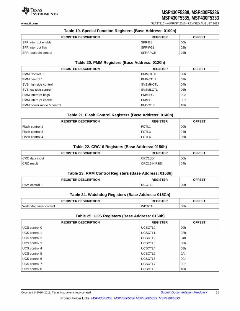
Table 19. Special Function Registers (Base Address: 0100h)REGISTER DESCRIPTION REGISTER OFFSET
SFR interrupt enable SFRIE1 00hSFR interrupt flag SFRIFG1 02hSFR reset pin control SFRRPCR 04h
Table 20. PMM Registers (Base Address: 0120h)REGISTER DESCRIPTION REGISTER OFFSET
PMM Control 0 PMMCTL0 00hPMM control 1 PMMCTL1 02hSVS high side control SVSMHCTL 04hSVS low side control SVSMLCTL 06hPMM interrupt flags PMMIFG 0ChPMM interrupt enable PMMIE 0EhPMM power mode 5 control PM5CTL0 10h
Table 21. Flash Control Registers (Base Address: 0140h)REGISTER DESCRIPTION REGISTER OFFSET
Flash control 1 FCTL1 00hFlash control 3 FCTL3 04hFlash control 4 FCTL4 06h
Table 22. CRC16 Registers (Base Address: 0150h)REGISTER DESCRIPTION REGISTER OFFSET
CRC data input CRC16DI 00hCRC result CRC16INIRES 04h
Table 23. RAM Control Registers (Base Address: 0158h)REGISTER DESCRIPTION REGISTER OFFSET
RAM control 0 RCCTL0 00h
Table 24. Watchdog Registers (Base Address: 015Ch)REGISTER DESCRIPTION REGISTER OFFSET
Watchdog timer control WDTCTL 00h
Table 25. UCS Registers (Base Address: 0160h)REGISTER DESCRIPTION REGISTER OFFSET
UCS control 0 UCSCTL0 00hUCS control 1 UCSCTL1 02hUCS control 2 UCSCTL2 04hUCS control 3 UCSCTL3 06hUCS control 4 UCSCTL4 08hUCS control 5 UCSCTL5 0AhUCS control 6 UCSCTL6 0ChUCS control 7 UCSCTL7 0EhUCS control 8 UCSCTL8 10h
Copyright © 2010–2013, Texas Instruments Incorporated Submit Documentation Feedback 31
Product Folder Links: MSP430F5338 MSP430F5336 MSP430F5335 MSP430F5333
MSP430F5338, MSP430F5336MSP430F5335, MSP430F5333SLAS721C –AUGUST 2010–REVISED AUGUST 2013 www.ti.com
Table 26. SYS Registers (Base Address: 0180h)REGISTER DESCRIPTION REGISTER OFFSET
System control SYSCTL 00hBootstrap loader configuration area SYSBSLC 02hJTAG mailbox control SYSJMBC 06hJTAG mailbox input 0 SYSJMBI0 08hJTAG mailbox input 1 SYSJMBI1 0AhJTAG mailbox output 0 SYSJMBO0 0ChJTAG mailbox output 1 SYSJMBO1 0EhBus Error vector generator SYSBERRIV 18hUser NMI vector generator SYSUNIV 1AhSystem NMI vector generator SYSSNIV 1ChReset vector generator SYSRSTIV 1Eh
Table 27. Shared Reference Registers (Base Address: 01B0h)REGISTER DESCRIPTION REGISTER OFFSET
Shared reference control REFCTL 00h
Table 28. Port Mapping Registers(Base Address of Port Mapping Control: 01C0h, Port P2: 01D0h)REGISTER DESCRIPTION REGISTER OFFSET
Port mapping password register PMAPPWD 00hPort mapping control register PMAPCTL 02hPort P2.0 mapping register P2MAP0 00hPort P2.1 mapping register P2MAP1 01hPort P2.2 mapping register P2MAP2 02hPort P2.3 mapping register P2MAP3 03hPort P2.4 mapping register P2MAP4 04hPort P2.5 mapping register P2MAP5 05hPort P2.6 mapping register P2MAP6 06hPort P2.7 mapping register P2MAP7 07h
Table 29. Port P1/P2 Registers (Base Address: 0200h)REGISTER DESCRIPTION REGISTER OFFSET
Port P1 input P1IN 00hPort P1 output P1OUT 02hPort P1 direction P1DIR 04hPort P1 pullup/pulldown enable P1REN 06hPort P1 drive strength P1DS 08hPort P1 selection P1SEL 0AhPort P1 interrupt vector word P1IV 0EhPort P1 interrupt edge select P1IES 18hPort P1 interrupt enable P1IE 1AhPort P1 interrupt flag P1IFG 1ChPort P2 input P2IN 01hPort P2 output P2OUT 03hPort P2 direction P2DIR 05hPort P2 pullup/pulldown enable P2REN 07hPort P2 drive strength P2DS 09h
32 Submit Documentation Feedback Copyright © 2010–2013, Texas Instruments Incorporated
Product Folder Links: MSP430F5338 MSP430F5336 MSP430F5335 MSP430F5333
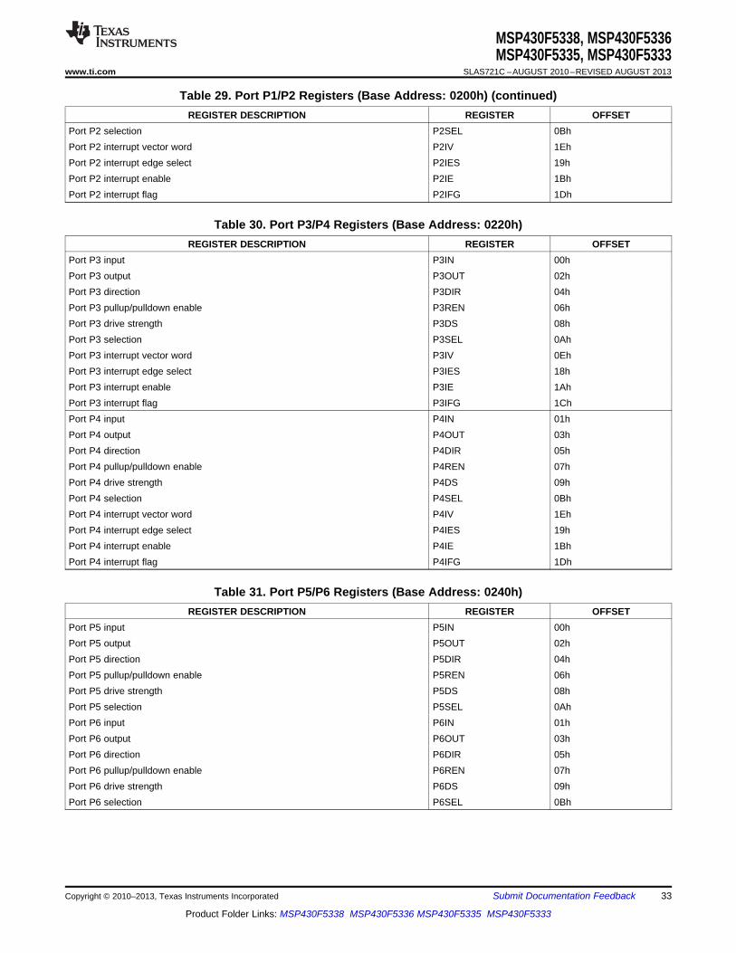
MSP430F5338, MSP430F5336MSP430F5335, MSP430F5333
www.ti.com SLAS721C –AUGUST 2010–REVISED AUGUST 2013
Table 29. Port P1/P2 Registers (Base Address: 0200h) (continued)REGISTER DESCRIPTION REGISTER OFFSET
Port P2 selection P2SEL 0BhPort P2 interrupt vector word P2IV 1EhPort P2 interrupt edge select P2IES 19hPort P2 interrupt enable P2IE 1BhPort P2 interrupt flag P2IFG 1Dh
Table 30. Port P3/P4 Registers (Base Address: 0220h)REGISTER DESCRIPTION REGISTER OFFSET
Port P3 input P3IN 00hPort P3 output P3OUT 02hPort P3 direction P3DIR 04hPort P3 pullup/pulldown enable P3REN 06hPort P3 drive strength P3DS 08hPort P3 selection P3SEL 0AhPort P3 interrupt vector word P3IV 0EhPort P3 interrupt edge select P3IES 18hPort P3 interrupt enable P3IE 1AhPort P3 interrupt flag P3IFG 1ChPort P4 input P4IN 01hPort P4 output P4OUT 03hPort P4 direction P4DIR 05hPort P4 pullup/pulldown enable P4REN 07hPort P4 drive strength P4DS 09hPort P4 selection P4SEL 0BhPort P4 interrupt vector word P4IV 1EhPort P4 interrupt edge select P4IES 19hPort P4 interrupt enable P4IE 1BhPort P4 interrupt flag P4IFG 1Dh
Table 31. Port P5/P6 Registers (Base Address: 0240h)REGISTER DESCRIPTION REGISTER OFFSET
Port P5 input P5IN 00hPort P5 output P5OUT 02hPort P5 direction P5DIR 04hPort P5 pullup/pulldown enable P5REN 06hPort P5 drive strength P5DS 08hPort P5 selection P5SEL 0AhPort P6 input P6IN 01hPort P6 output P6OUT 03hPort P6 direction P6DIR 05hPort P6 pullup/pulldown enable P6REN 07hPort P6 drive strength P6DS 09hPort P6 selection P6SEL 0Bh
Copyright © 2010–2013, Texas Instruments Incorporated Submit Documentation Feedback 33
Product Folder Links: MSP430F5338 MSP430F5336 MSP430F5335 MSP430F5333
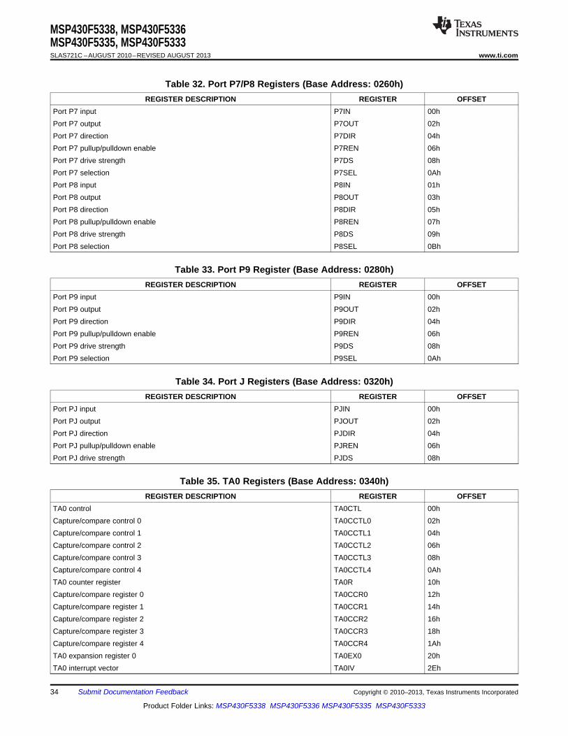
MSP430F5338, MSP430F5336MSP430F5335, MSP430F5333SLAS721C –AUGUST 2010–REVISED AUGUST 2013 www.ti.com
Table 32. Port P7/P8 Registers (Base Address: 0260h)REGISTER DESCRIPTION REGISTER OFFSET
Port P7 input P7IN 00hPort P7 output P7OUT 02hPort P7 direction P7DIR 04hPort P7 pullup/pulldown enable P7REN 06hPort P7 drive strength P7DS 08hPort P7 selection P7SEL 0AhPort P8 input P8IN 01hPort P8 output P8OUT 03hPort P8 direction P8DIR 05hPort P8 pullup/pulldown enable P8REN 07hPort P8 drive strength P8DS 09hPort P8 selection P8SEL 0Bh
Table 33. Port P9 Register (Base Address: 0280h)REGISTER DESCRIPTION REGISTER OFFSET
Port P9 input P9IN 00hPort P9 output P9OUT 02hPort P9 direction P9DIR 04hPort P9 pullup/pulldown enable P9REN 06hPort P9 drive strength P9DS 08hPort P9 selection P9SEL 0Ah
Table 34. Port J Registers (Base Address: 0320h)REGISTER DESCRIPTION REGISTER OFFSET
Port PJ input PJIN 00hPort PJ output PJOUT 02hPort PJ direction PJDIR 04hPort PJ pullup/pulldown enable PJREN 06hPort PJ drive strength PJDS 08h
Table 35. TA0 Registers (Base Address: 0340h)REGISTER DESCRIPTION REGISTER OFFSET
TA0 control TA0CTL 00hCapture/compare control 0 TA0CCTL0 02hCapture/compare control 1 TA0CCTL1 04hCapture/compare control 2 TA0CCTL2 06hCapture/compare control 3 TA0CCTL3 08hCapture/compare control 4 TA0CCTL4 0AhTA0 counter register TA0R 10hCapture/compare register 0 TA0CCR0 12hCapture/compare register 1 TA0CCR1 14hCapture/compare register 2 TA0CCR2 16hCapture/compare register 3 TA0CCR3 18hCapture/compare register 4 TA0CCR4 1AhTA0 expansion register 0 TA0EX0 20hTA0 interrupt vector TA0IV 2Eh
34 Submit Documentation Feedback Copyright © 2010–2013, Texas Instruments Incorporated
Product Folder Links: MSP430F5338 MSP430F5336 MSP430F5335 MSP430F5333
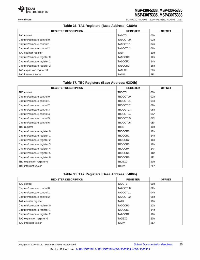
MSP430F5338, MSP430F5336MSP430F5335, MSP430F5333
www.ti.com SLAS721C –AUGUST 2010–REVISED AUGUST 2013
Table 36. TA1 Registers (Base Address: 0380h)REGISTER DESCRIPTION REGISTER OFFSET
TA1 control TA1CTL 00hCapture/compare control 0 TA1CCTL0 02hCapture/compare control 1 TA1CCTL1 04hCapture/compare control 2 TA1CCTL2 06hTA1 counter register TA1R 10hCapture/compare register 0 TA1CCR0 12hCapture/compare register 1 TA1CCR1 14hCapture/compare register 2 TA1CCR2 16hTA1 expansion register 0 TA1EX0 20hTA1 interrupt vector TA1IV 2Eh
Table 37. TB0 Registers (Base Address: 03C0h)REGISTER DESCRIPTION REGISTER OFFSET
TB0 control TB0CTL 00hCapture/compare control 0 TB0CCTL0 02hCapture/compare control 1 TB0CCTL1 04hCapture/compare control 2 TB0CCTL2 06hCapture/compare control 3 TB0CCTL3 08hCapture/compare control 4 TB0CCTL4 0AhCapture/compare control 5 TB0CCTL5 0ChCapture/compare control 6 TB0CCTL6 0EhTB0 register TB0R 10hCapture/compare register 0 TB0CCR0 12hCapture/compare register 1 TB0CCR1 14hCapture/compare register 2 TB0CCR2 16hCapture/compare register 3 TB0CCR3 18hCapture/compare register 4 TB0CCR4 1AhCapture/compare register 5 TB0CCR5 1ChCapture/compare register 6 TB0CCR6 1EhTB0 expansion register 0 TB0EX0 20hTB0 interrupt vector TB0IV 2Eh
Table 38. TA2 Registers (Base Address: 0400h)REGISTER DESCRIPTION REGISTER OFFSET
TA2 control TA2CTL 00hCapture/compare control 0 TA2CCTL0 02hCapture/compare control 1 TA2CCTL1 04hCapture/compare control 2 TA2CCTL2 06hTA2 counter register TA2R 10hCapture/compare register 0 TA2CCR0 12hCapture/compare register 1 TA2CCR1 14hCapture/compare register 2 TA2CCR2 16hTA2 expansion register 0 TA2EX0 20hTA2 interrupt vector TA2IV 2Eh
Copyright © 2010–2013, Texas Instruments Incorporated Submit Documentation Feedback 35
Product Folder Links: MSP430F5338 MSP430F5336 MSP430F5335 MSP430F5333
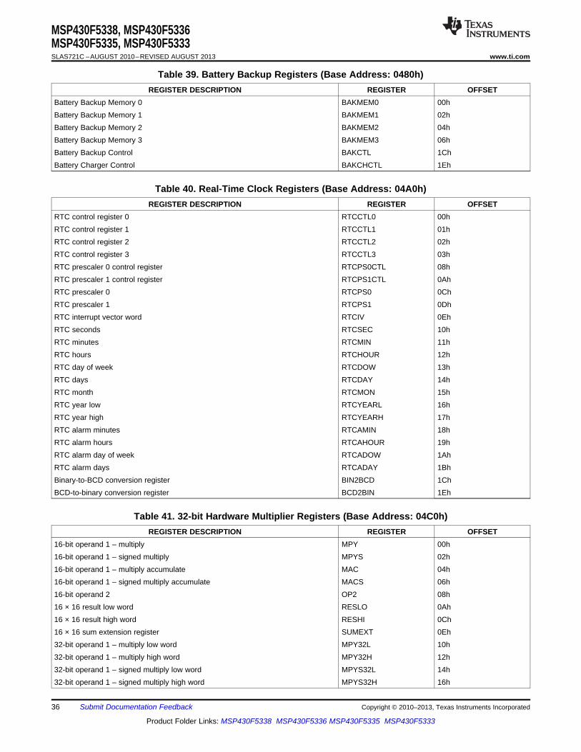
MSP430F5338, MSP430F5336MSP430F5335, MSP430F5333SLAS721C –AUGUST 2010–REVISED AUGUST 2013 www.ti.com
Table 39. Battery Backup Registers (Base Address: 0480h)REGISTER DESCRIPTION REGISTER OFFSET
Battery Backup Memory 0 BAKMEM0 00hBattery Backup Memory 1 BAKMEM1 02hBattery Backup Memory 2 BAKMEM2 04hBattery Backup Memory 3 BAKMEM3 06hBattery Backup Control BAKCTL 1ChBattery Charger Control BAKCHCTL 1Eh
Table 40. Real-Time Clock Registers (Base Address: 04A0h)REGISTER DESCRIPTION REGISTER OFFSET
RTC control register 0 RTCCTL0 00hRTC control register 1 RTCCTL1 01hRTC control register 2 RTCCTL2 02hRTC control register 3 RTCCTL3 03hRTC prescaler 0 control register RTCPS0CTL 08hRTC prescaler 1 control register RTCPS1CTL 0AhRTC prescaler 0 RTCPS0 0ChRTC prescaler 1 RTCPS1 0DhRTC interrupt vector word RTCIV 0EhRTC seconds RTCSEC 10hRTC minutes RTCMIN 11hRTC hours RTCHOUR 12hRTC day of week RTCDOW 13hRTC days RTCDAY 14hRTC month RTCMON 15hRTC year low RTCYEARL 16hRTC year high RTCYEARH 17hRTC alarm minutes RTCAMIN 18hRTC alarm hours RTCAHOUR 19hRTC alarm day of week RTCADOW 1AhRTC alarm days RTCADAY 1BhBinary-to-BCD conversion register BIN2BCD 1ChBCD-to-binary conversion register BCD2BIN 1Eh
Table 41. 32-bit Hardware Multiplier Registers (Base Address: 04C0h)REGISTER DESCRIPTION REGISTER OFFSET
16-bit operand 1 – multiply MPY 00h16-bit operand 1 – signed multiply MPYS 02h16-bit operand 1 – multiply accumulate MAC 04h16-bit operand 1 – signed multiply accumulate MACS 06h16-bit operand 2 OP2 08h16 × 16 result low word RESLO 0Ah16 × 16 result high word RESHI 0Ch16 × 16 sum extension register SUMEXT 0Eh32-bit operand 1 – multiply low word MPY32L 10h32-bit operand 1 – multiply high word MPY32H 12h32-bit operand 1 – signed multiply low word MPYS32L 14h32-bit operand 1 – signed multiply high word MPYS32H 16h
36 Submit Documentation Feedback Copyright © 2010–2013, Texas Instruments Incorporated
Product Folder Links: MSP430F5338 MSP430F5336 MSP430F5335 MSP430F5333
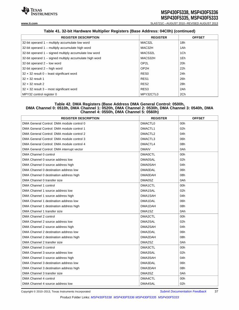
MSP430F5338, MSP430F5336MSP430F5335, MSP430F5333
www.ti.com SLAS721C –AUGUST 2010–REVISED AUGUST 2013
Table 41. 32-bit Hardware Multiplier Registers (Base Address: 04C0h) (continued)REGISTER DESCRIPTION REGISTER OFFSET
32-bit operand 1 – multiply accumulate low word MAC32L 18h32-bit operand 1 – multiply accumulate high word MAC32H 1Ah32-bit operand 1 – signed multiply accumulate low word MACS32L 1Ch32-bit operand 1 – signed multiply accumulate high word MACS32H 1Eh32-bit operand 2 – low word OP2L 20h32-bit operand 2 – high word OP2H 22h32 × 32 result 0 – least significant word RES0 24h32 × 32 result 1 RES1 26h32 × 32 result 2 RES2 28h32 × 32 result 3 – most significant word RES3 2AhMPY32 control register 0 MPY32CTL0 2Ch
Table 42. DMA Registers (Base Address DMA General Control: 0500h,DMA Channel 0: 0510h, DMA Channel 1: 0520h, DMA Channel 2: 0530h, DMA Channel 3: 0540h, DMA
Channel 4: 0550h, DMA Channel 5: 0560h)REGISTER DESCRIPTION REGISTER OFFSET
DMA General Control: DMA module control 0 DMACTL0 00hDMA General Control: DMA module control 1 DMACTL1 02hDMA General Control: DMA module control 2 DMACTL2 04hDMA General Control: DMA module control 3 DMACTL3 06hDMA General Control: DMA module control 4 DMACTL4 08hDMA General Control: DMA interrupt vector DMAIV 0AhDMA Channel 0 control DMA0CTL 00hDMA Channel 0 source address low DMA0SAL 02hDMA Channel 0 source address high DMA0SAH 04hDMA Channel 0 destination address low DMA0DAL 06hDMA Channel 0 destination address high DMA0DAH 08hDMA Channel 0 transfer size DMA0SZ 0AhDMA Channel 1 control DMA1CTL 00hDMA Channel 1 source address low DMA1SAL 02hDMA Channel 1 source address high DMA1SAH 04hDMA Channel 1 destination address low DMA1DAL 06hDMA Channel 1 destination address high DMA1DAH 08hDMA Channel 1 transfer size DMA1SZ 0AhDMA Channel 2 control DMA2CTL 00hDMA Channel 2 source address low DMA2SAL 02hDMA Channel 2 source address high DMA2SAH 04hDMA Channel 2 destination address low DMA2DAL 06hDMA Channel 2 destination address high DMA2DAH 08hDMA Channel 2 transfer size DMA2SZ 0AhDMA Channel 3 control DMA3CTL 00hDMA Channel 3 source address low DMA3SAL 02hDMA Channel 3 source address high DMA3SAH 04hDMA Channel 3 destination address low DMA3DAL 06hDMA Channel 3 destination address high DMA3DAH 08hDMA Channel 3 transfer size DMA3SZ 0AhDMA Channel 4 control DMA4CTL 00hDMA Channel 4 source address low DMA4SAL 02h
Copyright © 2010–2013, Texas Instruments Incorporated Submit Documentation Feedback 37
Product Folder Links: MSP430F5338 MSP430F5336 MSP430F5335 MSP430F5333
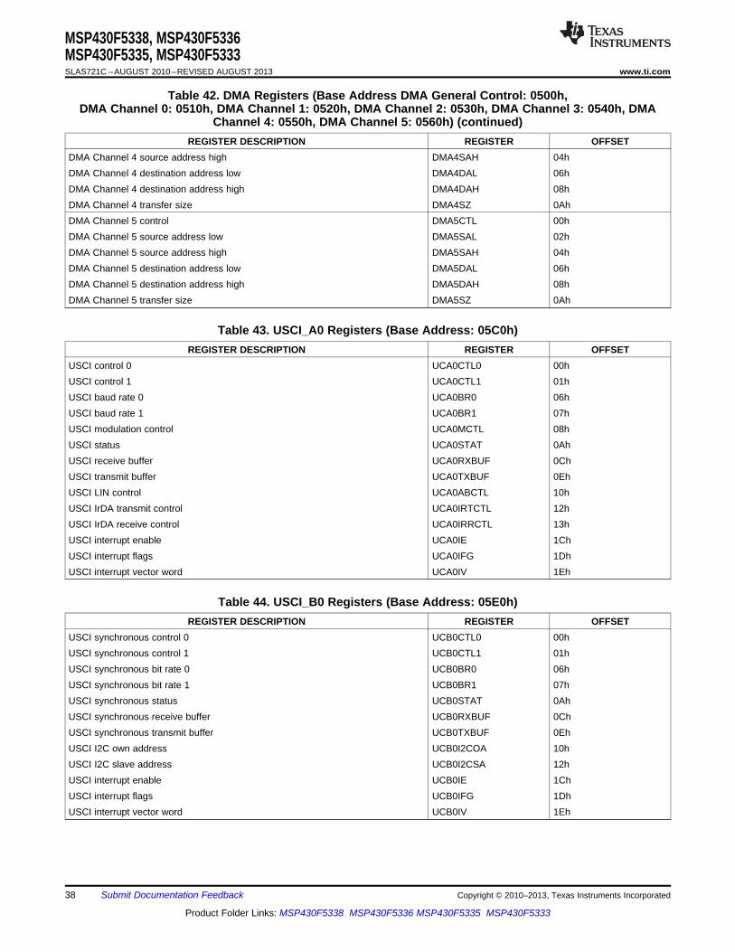
MSP430F5338, MSP430F5336MSP430F5335, MSP430F5333SLAS721C –AUGUST 2010–REVISED AUGUST 2013 www.ti.com
Table 42. DMA Registers (Base Address DMA General Control: 0500h,DMA Channel 0: 0510h, DMA Channel 1: 0520h, DMA Channel 2: 0530h, DMA Channel 3: 0540h, DMA
Channel 4: 0550h, DMA Channel 5: 0560h) (continued)REGISTER DESCRIPTION REGISTER OFFSET
DMA Channel 4 source address high DMA4SAH 04hDMA Channel 4 destination address low DMA4DAL 06hDMA Channel 4 destination address high DMA4DAH 08hDMA Channel 4 transfer size DMA4SZ 0AhDMA Channel 5 control DMA5CTL 00hDMA Channel 5 source address low DMA5SAL 02hDMA Channel 5 source address high DMA5SAH 04hDMA Channel 5 destination address low DMA5DAL 06hDMA Channel 5 destination address high DMA5DAH 08hDMA Channel 5 transfer size DMA5SZ 0Ah
Table 43. USCI_A0 Registers (Base Address: 05C0h)REGISTER DESCRIPTION REGISTER OFFSET
USCI control 0 UCA0CTL0 00hUSCI control 1 UCA0CTL1 01hUSCI baud rate 0 UCA0BR0 06hUSCI baud rate 1 UCA0BR1 07hUSCI modulation control UCA0MCTL 08hUSCI status UCA0STAT 0AhUSCI receive buffer UCA0RXBUF 0ChUSCI transmit buffer UCA0TXBUF 0EhUSCI LIN control UCA0ABCTL 10hUSCI IrDA transmit control UCA0IRTCTL 12hUSCI IrDA receive control UCA0IRRCTL 13hUSCI interrupt enable UCA0IE 1ChUSCI interrupt flags UCA0IFG 1DhUSCI interrupt vector word UCA0IV 1Eh
Table 44. USCI_B0 Registers (Base Address: 05E0h)REGISTER DESCRIPTION REGISTER OFFSET
USCI synchronous control 0 UCB0CTL0 00hUSCI synchronous control 1 UCB0CTL1 01hUSCI synchronous bit rate 0 UCB0BR0 06hUSCI synchronous bit rate 1 UCB0BR1 07hUSCI synchronous status UCB0STAT 0AhUSCI synchronous receive buffer UCB0RXBUF 0ChUSCI synchronous transmit buffer UCB0TXBUF 0EhUSCI I2C own address UCB0I2COA 10hUSCI I2C slave address UCB0I2CSA 12hUSCI interrupt enable UCB0IE 1ChUSCI interrupt flags UCB0IFG 1DhUSCI interrupt vector word UCB0IV 1Eh
38 Submit Documentation Feedback Copyright © 2010–2013, Texas Instruments Incorporated
Product Folder Links: MSP430F5338 MSP430F5336 MSP430F5335 MSP430F5333
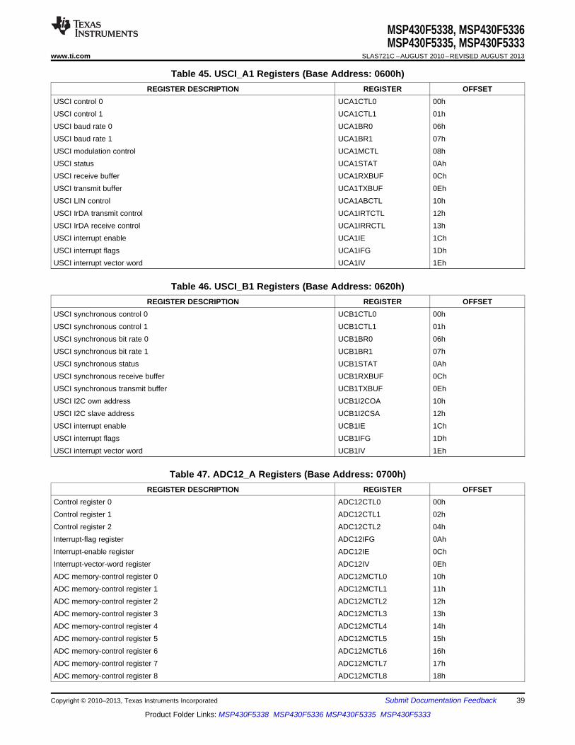
MSP430F5338, MSP430F5336MSP430F5335, MSP430F5333
www.ti.com SLAS721C –AUGUST 2010–REVISED AUGUST 2013
Table 45. USCI_A1 Registers (Base Address: 0600h)REGISTER DESCRIPTION REGISTER OFFSET
USCI control 0 UCA1CTL0 00hUSCI control 1 UCA1CTL1 01hUSCI baud rate 0 UCA1BR0 06hUSCI baud rate 1 UCA1BR1 07hUSCI modulation control UCA1MCTL 08hUSCI status UCA1STAT 0AhUSCI receive buffer UCA1RXBUF 0ChUSCI transmit buffer UCA1TXBUF 0EhUSCI LIN control UCA1ABCTL 10hUSCI IrDA transmit control UCA1IRTCTL 12hUSCI IrDA receive control UCA1IRRCTL 13hUSCI interrupt enable UCA1IE 1ChUSCI interrupt flags UCA1IFG 1DhUSCI interrupt vector word UCA1IV 1Eh
Table 46. USCI_B1 Registers (Base Address: 0620h)REGISTER DESCRIPTION REGISTER OFFSET
USCI synchronous control 0 UCB1CTL0 00hUSCI synchronous control 1 UCB1CTL1 01hUSCI synchronous bit rate 0 UCB1BR0 06hUSCI synchronous bit rate 1 UCB1BR1 07hUSCI synchronous status UCB1STAT 0AhUSCI synchronous receive buffer UCB1RXBUF 0ChUSCI synchronous transmit buffer UCB1TXBUF 0EhUSCI I2C own address UCB1I2COA 10hUSCI I2C slave address UCB1I2CSA 12hUSCI interrupt enable UCB1IE 1ChUSCI interrupt flags UCB1IFG 1DhUSCI interrupt vector word UCB1IV 1Eh
Table 47. ADC12_A Registers (Base Address: 0700h)REGISTER DESCRIPTION REGISTER OFFSET
Control register 0 ADC12CTL0 00hControl register 1 ADC12CTL1 02hControl register 2 ADC12CTL2 04hInterrupt-flag register ADC12IFG 0AhInterrupt-enable register ADC12IE 0ChInterrupt-vector-word register ADC12IV 0EhADC memory-control register 0 ADC12MCTL0 10hADC memory-control register 1 ADC12MCTL1 11hADC memory-control register 2 ADC12MCTL2 12hADC memory-control register 3 ADC12MCTL3 13hADC memory-control register 4 ADC12MCTL4 14hADC memory-control register 5 ADC12MCTL5 15hADC memory-control register 6 ADC12MCTL6 16hADC memory-control register 7 ADC12MCTL7 17hADC memory-control register 8 ADC12MCTL8 18h
Copyright © 2010–2013, Texas Instruments Incorporated Submit Documentation Feedback 39
Product Folder Links: MSP430F5338 MSP430F5336 MSP430F5335 MSP430F5333
MSP430F5338, MSP430F5336MSP430F5335, MSP430F5333SLAS721C –AUGUST 2010–REVISED AUGUST 2013 www.ti.com
Table 47. ADC12_A Registers (Base Address: 0700h) (continued)REGISTER DESCRIPTION REGISTER OFFSET
ADC memory-control register 9 ADC12MCTL9 19hADC memory-control register 10 ADC12MCTL10 1AhADC memory-control register 11 ADC12MCTL11 1BhADC memory-control register 12 ADC12MCTL12 1ChADC memory-control register 13 ADC12MCTL13 1DhADC memory-control register 14 ADC12MCTL14 1EhADC memory-control register 15 ADC12MCTL15 1FhConversion memory 0 ADC12MEM0 20hConversion memory 1 ADC12MEM1 22hConversion memory 2 ADC12MEM2 24hConversion memory 3 ADC12MEM3 26hConversion memory 4 ADC12MEM4 28hConversion memory 5 ADC12MEM5 2AhConversion memory 6 ADC12MEM6 2ChConversion memory 7 ADC12MEM7 2EhConversion memory 8 ADC12MEM8 30hConversion memory 9 ADC12MEM9 32hConversion memory 10 ADC12MEM10 34hConversion memory 11 ADC12MEM11 36hConversion memory 12 ADC12MEM12 38hConversion memory 13 ADC12MEM13 3AhConversion memory 14 ADC12MEM14 3ChConversion memory 15 ADC12MEM15 3Eh
Table 48. DAC12_A Registers (Base Address: 0780h)REGISTER DESCRIPTION REGISTER OFFSET
DAC12_A channel 0 control register 0 DAC12_0CTL0 00hDAC12_A channel 0 control register 1 DAC12_0CTL1 02hDAC12_A channel 0 data register DAC12_0DAT 04hDAC12_A channel 0 calibration control register DAC12_0CALCTL 06hDAC12_A channel 0 calibration data register DAC12_0CALDAT 08hDAC12_A channel 1 control register 0 DAC12_1CTL0 10hDAC12_A channel 1 control register 1 DAC12_1CTL1 12hDAC12_A channel 1 data register DAC12_1DAT 14hDAC12_A channel 1 calibration control register DAC12_1CALCTL 16hDAC12_A channel 1 calibration data register DAC12_1CALDAT 18hDAC12_A interrupt vector word DAC12IV 1Eh
Table 49. Comparator_B Registers (Base Address: 08C0h)REGISTER DESCRIPTION REGISTER OFFSET
Comp_B control register 0 CBCTL0 00hComp_B control register 1 CBCTL1 02hComp_B control register 2 CBCTL2 04hComp_B control register 3 CBCTL3 06hComp_B interrupt register CBINT 0ChComp_B interrupt vector word CBIV 0Eh
40 Submit Documentation Feedback Copyright © 2010–2013, Texas Instruments Incorporated
Product Folder Links: MSP430F5338 MSP430F5336 MSP430F5335 MSP430F5333
MSP430F5338, MSP430F5336MSP430F5335, MSP430F5333
www.ti.com SLAS721C –AUGUST 2010–REVISED AUGUST 2013
Table 50. LDO and Port U Configuration Registers (Base Address: 0900h)REGISTER DESCRIPTION REGISTER OFFSET
LDO key/ID register LDOKEYID 00hPU port control PUCTL 04hLDO power control LDOPWRCTL 08h
Copyright © 2010–2013, Texas Instruments Incorporated Submit Documentation Feedback 41
Product Folder Links: MSP430F5338 MSP430F5336 MSP430F5335 MSP430F5333

MSP430F5338, MSP430F5336MSP430F5335, MSP430F5333SLAS721C –AUGUST 2010–REVISED AUGUST 2013 www.ti.com
Absolute Maximum Ratings (1)
over operating free-air temperature range (unless otherwise noted)Voltage applied at VCC to VSS –0.3 V to 4.1 VVoltage applied to any pin (excluding VCORE, VBUS, V18) (2) –0.3 V to VCC + 0.3 VDiode current at any device pin ±2 mAStorage temperature range, Tstg
(3) –55°C to 150°CMaximum junction temperature, TJ 95°C
(1) Stresses beyond those listed under "absolute maximum ratings" may cause permanent damage to the device. These are stress ratingsonly, and functional operation of the device at these or any other conditions beyond those indicated under "recommended operatingconditions" is not implied. Exposure to absolute-maximum-rated conditions for extended periods may affect device reliability.
(2) All voltages referenced to VSS. VCORE is for internal device use only. No external dc loading or voltage should be applied.(3) Higher temperature may be applied during board soldering according to the current JEDEC J-STD-020 specification with peak reflow
temperatures not higher than classified on the device label on the shipping boxes or reels.
Recommended Operating ConditionsMIN NOM MAX UNIT
PMMCOREVx = 0 1.8 3.6Supply voltage during program execution and flash PMMCOREVx = 0, 1 2.0 3.6
VCC programming (AVCC1 = DVCC1 = DVCC2 = DVCC3 = VPMMCOREVx = 0, 1, 2 2.2 3.6DVCC = VCC) (1) (2)
PMMCOREVx = 0, 1, 2, 3 2.4 3.6Supply voltage (AVSS1 = AVSS2 = AVSS3 = DVSS1 =VSS 0 VDVSS2 = DVSS3 = VSS)
TA = 0°C to 85°C 1.55 3.6VBAT,RTC Backup-supply voltage with RTC operational V
TA = –40°C to 85°C 1.70 3.6VBAT,MEM Backup-supply voltage with backup memory retained. TA = –40°C to 85°C 1.20 3.6 VTA Operating free-air temperature I version –40 85 °CTJ Operating junction temperature I version –40 85 °CCBAK Capacitance at pin VBAK 1 4.7 10 nFCVCORE Capacitor at VCORE 470 nFCDVCC/ Capacitor ratio of DVCC to VCORE 10CVCORE
PMMCOREVx = 0,1.8 V ≤ VCC ≤ 3.6 V 0 8.0(default condition)PMMCOREVx = 1, 0 12.0Processor frequency (maximum MCLK frequency) (3) (4)2 V ≤ VCC ≤ 3.6 VfSYSTEM MHz(see Figure 2)PMMCOREVx = 2, 0 16.02.2 V ≤ VCC ≤ 3.6 VPMMCOREVx = 3, 0 20.02.4 V ≤ VCC ≤ 3.6 V
(1) It is recommended to power AVCC and DVCC from the same source. A maximum difference of 0.3 V between AVCC and DVCC can betolerated during power up and operation.
(2) The minimum supply voltage is defined by the supervisor SVS levels when it is enabled. See the PMM, SVS High Side thresholdparameters for the exact values and further details.
(3) The MSP430 CPU is clocked directly with MCLK. Both the high and low phase of MCLK must not exceed the pulse duration of thespecified maximum frequency.
(4) Modules may have a different maximum input clock specification. See the specification of the respective module in this data sheet.
42 Submit Documentation Feedback Copyright © 2010–2013, Texas Instruments Incorporated
Product Folder Links: MSP430F5338 MSP430F5336 MSP430F5335 MSP430F5333
2.01.8
8
0
12
20
25
Syste
m F
requency -
MH
z
Supply Voltage - V
The numbers within the fields denote the supported PMMCOREVx settings.
2.2 2.4 3.6
0, 1, 2, 30, 1, 20, 10
1, 2, 31, 21
2, 3
3
2
16
MSP430F5338, MSP430F5336MSP430F5335, MSP430F5333
www.ti.com SLAS721C –AUGUST 2010–REVISED AUGUST 2013
Figure 2. Frequency vs Supply Voltage
Copyright © 2010–2013, Texas Instruments Incorporated Submit Documentation Feedback 43
Product Folder Links: MSP430F5338 MSP430F5336 MSP430F5335 MSP430F5333
MSP430F5338, MSP430F5336MSP430F5335, MSP430F5333SLAS721C –AUGUST 2010–REVISED AUGUST 2013 www.ti.com
Electrical Characteristics
Active Mode Supply Current Into VCC Excluding External Currentover recommended operating free-air temperature (unless otherwise noted) (1) (2) (3)
FREQUENCY (fDCO = fMCLK = fSMCLK)EXECUTIONPARAMETER VCC PMMCOREVx 1 MHz 8 MHz 12 MHz 20 MHz UNITMEMORY
TYP MAX TYP MAX TYP MAX TYP MAX0 0.32 0.36 2.1 2.41 0.36 2.4 3.6 4.0
IAM, Flash Flash 3 V mA2 0.37 2.5 3.83 0.39 2.7 4.0 6.60 0.18 0.21 1.0 1.21 0.20 1.2 1.7 1.9
IAM, RAM RAM 3 V mA2 0.22 1.3 2.03 0.23 1.4 2.1 3.6
(1) All inputs are tied to 0 V or to VCC. Outputs do not source or sink any current.(2) The currents are characterized with a Micro Crystal MS1V-T1K crystal with a load capacitance of 12.5 pF. The internal and external load
capacitance are chosen to closely match the required 12.5 pF.(3) Characterized with program executing typical data processing. LDO disabled (LDOEN = 0).
fACLK = 32786 Hz, fDCO = fMCLK = fSMCLK at specified frequency.XTS = CPUOFF = SCG0 = SCG1 = OSCOFF = SMCLKOFF = 0.
44 Submit Documentation Feedback Copyright © 2010–2013, Texas Instruments Incorporated
Product Folder Links: MSP430F5338 MSP430F5336 MSP430F5335 MSP430F5333
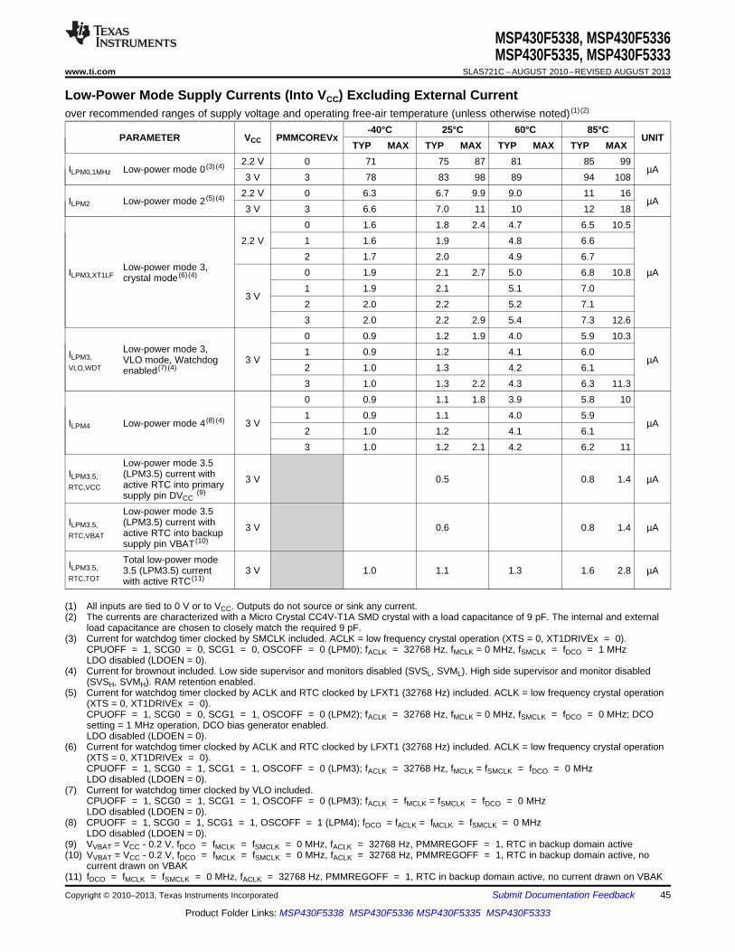
MSP430F5338, MSP430F5336MSP430F5335, MSP430F5333
www.ti.com SLAS721C –AUGUST 2010–REVISED AUGUST 2013
Low-Power Mode Supply Currents (Into VCC) Excluding External Currentover recommended ranges of supply voltage and operating free-air temperature (unless otherwise noted) (1) (2)
-40°C 25°C 60°C 85°CPARAMETER VCC PMMCOREVx UNIT
TYP MAX TYP MAX TYP MAX TYP MAX2.2 V 0 71 75 87 81 85 99
ILPM0,1MHz Low-power mode 0 (3) (4) µA3 V 3 78 83 98 89 94 108
2.2 V 0 6.3 6.7 9.9 9.0 11 16ILPM2 Low-power mode 2 (5) (4) µA
3 V 3 6.6 7.0 11 10 12 180 1.6 1.8 2.4 4.7 6.5 10.5
2.2 V 1 1.6 1.9 4.8 6.62 1.7 2.0 4.9 6.7
Low-power mode 3,ILPM3,XT1LF 0 1.9 2.1 2.7 5.0 6.8 10.8 µAcrystal mode (6) (4)
1 1.9 2.1 5.1 7.03 V
2 2.0 2.2 5.2 7.13 2.0 2.2 2.9 5.4 7.3 12.60 0.9 1.2 1.9 4.0 5.9 10.3
Low-power mode 3, 1 0.9 1.2 4.1 6.0ILPM3, VLO mode, Watchdog 3 V µAVLO,WDT 2 1.0 1.3 4.2 6.1enabled (7) (4)
3 1.0 1.3 2.2 4.3 6.3 11.30 0.9 1.1 1.8 3.9 5.8 101 0.9 1.1 4.0 5.9
ILPM4 Low-power mode 4 (8) (4) 3 V µA2 1.0 1.2 4.1 6.13 1.0 1.2 2.1 4.2 6.2 11
Low-power mode 3.5ILPM3.5, (LPM3.5) current with 3 V 0.5 0.8 1.4 µARTC,VCC active RTC into primary
supply pin DVCC(9)
Low-power mode 3.5ILPM3.5, (LPM3.5) current with 3 V 0.6 0.8 1.4 µARTC,VBAT active RTC into backup
supply pin VBAT (10)
Total low-power modeILPM3.5, 3.5 (LPM3.5) current 3 V 1.0 1.1 1.3 1.6 2.8 µARTC,TOT with active RTC (11)
(1) All inputs are tied to 0 V or to VCC. Outputs do not source or sink any current.(2) The currents are characterized with a Micro Crystal CC4V-T1A SMD crystal with a load capacitance of 9 pF. The internal and external
load capacitance are chosen to closely match the required 9 pF.(3) Current for watchdog timer clocked by SMCLK included. ACLK = low frequency crystal operation (XTS = 0, XT1DRIVEx = 0).
CPUOFF = 1, SCG0 = 0, SCG1 = 0, OSCOFF = 0 (LPM0); fACLK = 32768 Hz, fMCLK = 0 MHz, fSMCLK = fDCO = 1 MHzLDO disabled (LDOEN = 0).
(4) Current for brownout included. Low side supervisor and monitors disabled (SVSL, SVML). High side supervisor and monitor disabled(SVSH, SVMH). RAM retention enabled.
(5) Current for watchdog timer clocked by ACLK and RTC clocked by LFXT1 (32768 Hz) included. ACLK = low frequency crystal operation(XTS = 0, XT1DRIVEx = 0).CPUOFF = 1, SCG0 = 0, SCG1 = 1, OSCOFF = 0 (LPM2); fACLK = 32768 Hz, fMCLK = 0 MHz, fSMCLK = fDCO = 0 MHz; DCOsetting = 1 MHz operation, DCO bias generator enabled.LDO disabled (LDOEN = 0).
(6) Current for watchdog timer clocked by ACLK and RTC clocked by LFXT1 (32768 Hz) included. ACLK = low frequency crystal operation(XTS = 0, XT1DRIVEx = 0).CPUOFF = 1, SCG0 = 1, SCG1 = 1, OSCOFF = 0 (LPM3); fACLK = 32768 Hz, fMCLK = fSMCLK = fDCO = 0 MHzLDO disabled (LDOEN = 0).
(7) Current for watchdog timer clocked by VLO included.CPUOFF = 1, SCG0 = 1, SCG1 = 1, OSCOFF = 0 (LPM3); fACLK = fMCLK = fSMCLK = fDCO = 0 MHzLDO disabled (LDOEN = 0).
(8) CPUOFF = 1, SCG0 = 1, SCG1 = 1, OSCOFF = 1 (LPM4); fDCO = fACLK = fMCLK = fSMCLK = 0 MHzLDO disabled (LDOEN = 0).
(9) VVBAT = VCC - 0.2 V, fDCO = fMCLK = fSMCLK = 0 MHz, fACLK = 32768 Hz, PMMREGOFF = 1, RTC in backup domain active(10) VVBAT = VCC - 0.2 V, fDCO = fMCLK = fSMCLK = 0 MHz, fACLK = 32768 Hz, PMMREGOFF = 1, RTC in backup domain active, no
current drawn on VBAK(11) fDCO = fMCLK = fSMCLK = 0 MHz, fACLK = 32768 Hz, PMMREGOFF = 1, RTC in backup domain active, no current drawn on VBAK
Copyright © 2010–2013, Texas Instruments Incorporated Submit Documentation Feedback 45
Product Folder Links: MSP430F5338 MSP430F5336 MSP430F5335 MSP430F5333
MSP430F5338, MSP430F5336MSP430F5335, MSP430F5333SLAS721C –AUGUST 2010–REVISED AUGUST 2013 www.ti.com
Low-Power Mode Supply Currents (Into VCC) Excluding External Current (continued)over recommended ranges of supply voltage and operating free-air temperature (unless otherwise noted)(1)(2)
-40°C 25°C 60°C 85°CPARAMETER VCC PMMCOREVx UNIT
TYP MAX TYP MAX TYP MAX TYP MAXLow-power mode 4.5ILPM4.5 3 V 0.2 0.3 0.6 0.7 0.9 1.4 µA(LPM4.5) (12)
(12) Internal regulator disabled. No data retention.CPUOFF = 1, SCG0 = 1, SCG1 = 1, OSCOFF = 1, PMMREGOFF = 1 (LPM4.5); fDCO = fACLK = fMCLK = fSMCLK = 0 MHz
Schmitt-Trigger Inputs – General Purpose I/O (1)
over recommended ranges of supply voltage and operating free-air temperature (unless otherwise noted)PARAMETER TEST CONDITIONS VCC MIN TYP MAX UNIT
1.8 V 0.80 1.40VIT+ Positive-going input threshold voltage V
3 V 1.50 2.101.8 V 0.45 1.00
VIT– Negative-going input threshold voltage V3 V 0.75 1.65
1.8 V 0.3 0.8Vhys Input voltage hysteresis (VIT+ – VIT–) V
3 V 0.4 1.0For pullup: VIN = VSSRPull Pullup or pulldown resistor 20 35 50 kΩFor pulldown: VIN = VCC
CI Input capacitance VIN = VSS or VCC 5 pF
(1) Same parametrics apply to clock input pin when crystal bypass mode is used on XT1 (XIN) or XT2 (XT2IN).
Inputs – Ports P1, P2, P3, and P4 (1)
over recommended ranges of supply voltage and operating free-air temperature (unless otherwise noted)PARAMETER TEST CONDITIONS VCC MIN MAX UNIT
Port P1, P2, P3, P4: P1.x to P4.x,t(int) External interrupt timing (2) 2.2 V, 3 V 20 nsExternal trigger pulse duration to set interrupt flag
(1) Some devices may contain additional ports with interrupts. See the block diagram and terminal function descriptions.(2) An external signal sets the interrupt flag every time the minimum interrupt pulse duration t(int) is met. It may be set by trigger signals
shorter than t(int).
Leakage Current – General Purpose I/Oover recommended ranges of supply voltage and operating free-air temperature (unless otherwise noted)
PARAMETER TEST CONDITIONS VCC MIN MAX UNITIlkg(Px.x) High-impedance leakage current (1) (2) 1.8 V, 3 V ±50 nA
(1) The leakage current is measured with VSS or VCC applied to the corresponding pin(s), unless otherwise noted.(2) The leakage of the digital port pins is measured individually. The port pin is selected for input and the pullup or pulldown resistor is
disabled.
Outputs – General Purpose I/O (Full Drive Strength)over recommended ranges of supply voltage and operating free-air temperature (unless otherwise noted)
PARAMETER TEST CONDITIONS VCC MIN MAX UNITI(OHmax) = –3 mA (1) VCC – 0.25 VCC1.8 VI(OHmax) = –10 mA (2) VCC – 0.60 VCCVOH High-level output voltage VI(OHmax) = –5 mA (1) VCC – 0.25 VCC3 VI(OHmax) = –15 mA (2) VCC – 0.60 VCC
(1) The maximum total current, I(OHmax) and I(OLmax), for all outputs combined should not exceed ±48 mA to hold the maximum voltage dropspecified.
(2) The maximum total current, I(OHmax) and I(OLmax), for all outputs combined should not exceed ±100 mA to hold the maximum voltagedrop specified.
46 Submit Documentation Feedback Copyright © 2010–2013, Texas Instruments Incorporated
Product Folder Links: MSP430F5338 MSP430F5336 MSP430F5335 MSP430F5333
MSP430F5338, MSP430F5336MSP430F5335, MSP430F5333
www.ti.com SLAS721C –AUGUST 2010–REVISED AUGUST 2013
Outputs – General Purpose I/O (Full Drive Strength) (continued)over recommended ranges of supply voltage and operating free-air temperature (unless otherwise noted)
PARAMETER TEST CONDITIONS VCC MIN MAX UNITI(OLmax) = 3 mA (1) VSS VSS + 0.25
1.8 VI(OLmax) = 10 mA (2) VSS VSS + 0.60
VOL Low-level output voltage VI(OLmax) = 5 mA (1) VSS VSS + 0.25
3 VI(OLmax) = 15 mA (2) VSS VSS + 0.60
Outputs – General Purpose I/O (Reduced Drive Strength)over recommended ranges of supply voltage and operating free-air temperature (unless otherwise noted) (1)
PARAMETER TEST CONDITIONS VCC MIN MAX UNITI(OHmax) = –1 mA (2) VCC – 0.25 VCC1.8 VI(OHmax) = –3 mA (3) VCC – 0.60 VCCVOH High-level output voltage VI(OHmax) = –2 mA (2) VCC – 0.25 VCC3 VI(OHmax) = –6 mA (3) VCC – 0.60 VCC
I(OLmax) = 1 mA (2) VSS VSS + 0.251.8 V
I(OLmax) = 3 mA (3) VSS VSS + 0.60VOL Low-level output voltage V
I(OLmax) = 2 mA (2) VSS VSS + 0.253 V
I(OLmax) = 6 mA (3) VSS VSS + 0.60
(1) Selecting reduced drive strength may reduce EMI.(2) The maximum total current, I(OHmax) and I(OLmax), for all outputs combined, should not exceed ±48 mA to hold the maximum voltage drop
specified.(3) The maximum total current, I(OHmax) and I(OLmax), for all outputs combined, should not exceed ±100 mA to hold the maximum voltage
drop specified.
Output Frequency – Ports P1, P2, and P3over recommended ranges of supply voltage and operating free-air temperature (unless otherwise noted)
PARAMETER TEST CONDITIONS MIN MAX UNITVCC = 1.8 V 8PMMCOREVx = 0Port output frequency P3.4/TA2CLK/SMCLK/S27fPx.y MHz(with load) CL = 20 pF, RL = 1 kΩ (1) or 3.2 kΩ (2) (3) VCC = 3 V 20PMMCOREVx = 3VCC = 1.8 VP1.0/TA0CLK/ACLK/S39 8PMMCOREVx = 0P3.4/TA2CLK/SMCLK/S27fPort_CLK Clock output frequency MHzP2.0/P2MAP0 (P2MAP0 = PM_MCLK ) VCC = 3 V 20CL = 20 pF (3) PMMCOREVx = 3
(1) Full drive strength of port: A resistive divider with 2 × 0.5 kΩ between VCC and VSS is used as load. The output is connected to thecenter tap of the divider.
(2) Reduced drive strength of port: A resistive divider with 2 × 1.6 kΩ between VCC and VSS is used as load. The output is connected to thecenter tap of the divider.
(3) The output voltage reaches at least 10% and 90% VCC at the specified toggle frequency.
Copyright © 2010–2013, Texas Instruments Incorporated Submit Documentation Feedback 47
Product Folder Links: MSP430F5338 MSP430F5336 MSP430F5335 MSP430F5333
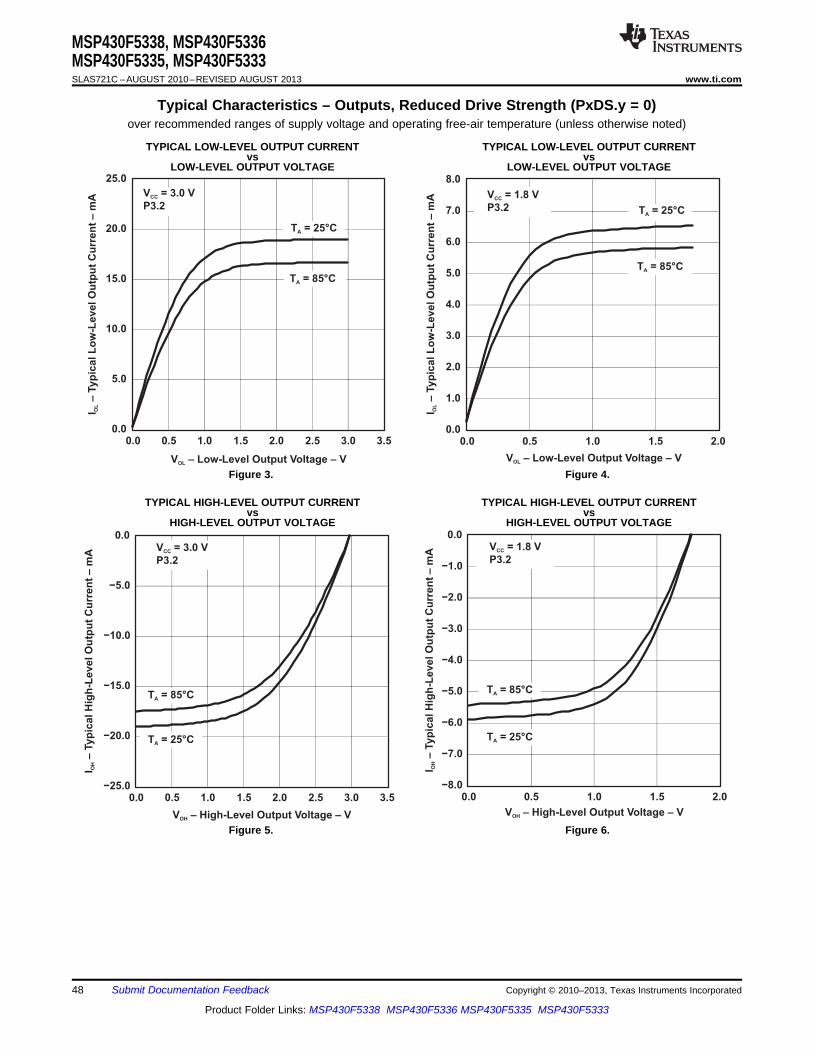
−25.0
−20.0
−15.0
−10.0
−5.0
0.0
0.0 0.5 1.0 1.5 2.0 2.5 3.0 3.5
T = 25°CA
T = 85°CA
V = 3.0 V
P3.2CC
V – High-Level Output Voltage – VOH
I–
Typ
ical H
igh
-Level O
utp
ut
Cu
rren
t–
mA
OH
−8.0
−7.0
−6.0
−5.0
−4.0
−3.0
−2.0
−1.0
0.0
0.0 0.5 1.0 1.5 2.0
T = 25°CA
T = 85°CA
V = 1.8 V
P3.2CC
V – High-Level Output Voltage – VOH
I–
Typ
ical H
igh
-Level O
utp
ut
Cu
rren
t–
mA
OH
0.0
5.0
10.0
15.0
20.0
25.0
0.0 0.5 1.0 1.5 2.0 2.5 3.0 3.5
T = 25°CA
T = 85°CA
V = 3.0 V
P3.2CC
V – Low-Level Output Voltage – VOL
I–
Typ
ical L
ow
-Level O
utp
ut
Cu
rren
t–
mA
OL
0.0
1.0
2.0
3.0
4.0
5.0
6.0
7.0
8.0
0.0 0.5 1.0 1.5 2.0
T = 25°CA
T = 85°CA
V = 1.8 V
P3.2CC
V – Low-Level Output Voltage – VOL
I–
Typ
ical L
ow
-Level O
utp
ut
Cu
rren
t–
mA
OL
MSP430F5338, MSP430F5336MSP430F5335, MSP430F5333SLAS721C –AUGUST 2010–REVISED AUGUST 2013 www.ti.com
Typical Characteristics – Outputs, Reduced Drive Strength (PxDS.y = 0)over recommended ranges of supply voltage and operating free-air temperature (unless otherwise noted)
TYPICAL LOW-LEVEL OUTPUT CURRENT TYPICAL LOW-LEVEL OUTPUT CURRENTvs vs
LOW-LEVEL OUTPUT VOLTAGE LOW-LEVEL OUTPUT VOLTAGE
Figure 3. Figure 4.
TYPICAL HIGH-LEVEL OUTPUT CURRENT TYPICAL HIGH-LEVEL OUTPUT CURRENTvs vs
HIGH-LEVEL OUTPUT VOLTAGE HIGH-LEVEL OUTPUT VOLTAGE
Figure 5. Figure 6.
48 Submit Documentation Feedback Copyright © 2010–2013, Texas Instruments Incorporated
Product Folder Links: MSP430F5338 MSP430F5336 MSP430F5335 MSP430F5333
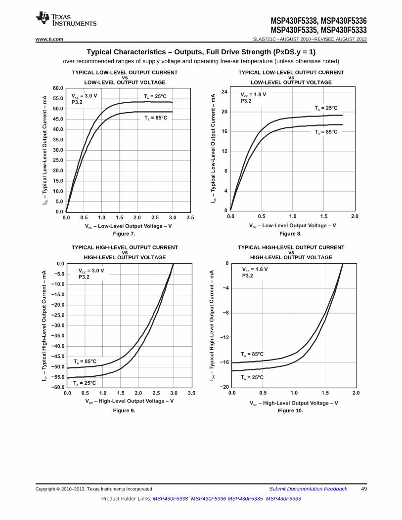
−20
−16
−12
−8
−4
0
0.0 0.5 1.0 1.5 2.0
T = 25°CA
T = 85°CA
V = 1.8 V
P3.2CC
V – High-Level Output Voltage – VOH
I–
Typ
ical H
igh
-Level O
utp
ut
Cu
rren
t–
mA
OH
−60.0
−55.0
−50.0
−45.0
−40.0
−35.0
−30.0
−25.0
−20.0
−15.0
−10.0
−5.0
0.0
0.0 0.5 1.0 1.5 2.0 2.5 3.0 3.5
T = 25°CA
T = 85°CA
V = 3.0 V
P3.2CC
V – High-Level Output Voltage – VOH
I–
Typ
ical H
igh
-Level O
utp
ut
Cu
rren
t–
mA
OH
0.0
5.0
10.0
15.0
20.0
25.0
30.0
35.0
40.0
45.0
50.0
55.0
60.0
0.0 0.5 1.0 1.5 2.0 2.5 3.0 3.5
T = 25°CA
T = 85°CA
V = 3.0 V
P3.2CC
V – Low-Level Output Voltage – VOL
I–
Typ
ical L
ow
-Level O
utp
ut
Cu
rren
t–
mA
OL
0
4
8
12
16
20
24
0.0 0.5 1.0 1.5 2.0
T = 25°CA
T = 85°CA
V = 1.8 V
P3.2CC
V – Low-Level Output Voltage – VOL
I–
Typ
ical L
ow
-Level O
utp
ut
Cu
rren
t–
mA
OL
MSP430F5338, MSP430F5336MSP430F5335, MSP430F5333
www.ti.com SLAS721C –AUGUST 2010–REVISED AUGUST 2013
Typical Characteristics – Outputs, Full Drive Strength (PxDS.y = 1)over recommended ranges of supply voltage and operating free-air temperature (unless otherwise noted)
TYPICAL LOW-LEVEL OUTPUT CURRENT TYPICAL LOW-LEVEL OUTPUT CURRENTvs vs
LOW-LEVEL OUTPUT VOLTAGE LOW-LEVEL OUTPUT VOLTAGE
Figure 7. Figure 8.
TYPICAL HIGH-LEVEL OUTPUT CURRENT TYPICAL HIGH-LEVEL OUTPUT CURRENTvs vs
HIGH-LEVEL OUTPUT VOLTAGE HIGH-LEVEL OUTPUT VOLTAGE
Figure 9. Figure 10.
Copyright © 2010–2013, Texas Instruments Incorporated Submit Documentation Feedback 49
Product Folder Links: MSP430F5338 MSP430F5336 MSP430F5335 MSP430F5333

MSP430F5338, MSP430F5336MSP430F5335, MSP430F5333SLAS721C –AUGUST 2010–REVISED AUGUST 2013 www.ti.com
Crystal Oscillator, XT1, Low-Frequency Mode (1)
over recommended ranges of supply voltage and operating free-air temperature (unless otherwise noted)PARAMETER TEST CONDITIONS VCC MIN TYP MAX UNIT
fOSC = 32768 Hz, XTS = 0,XT1BYPASS = 0, XT1DRIVEx = 1, 0.075TA = 25°C
Differential XT1 oscillator crystal fOSC = 32768 Hz, XTS = 0,ΔIDVCC,LF current consumption from lowest XT1BYPASS = 0, XT1DRIVEx = 2, 3 V 0.170 µA
drive setting, LF mode TA = 25°CfOSC = 32768 Hz, XTS = 0,XT1BYPASS = 0, XT1DRIVEx = 3, 0.290TA = 25°C
XT1 oscillator crystal frequency,fXT1,LF0 XTS = 0, XT1BYPASS = 0 32768 HzLF modeXT1 oscillator logic-level square-fXT1,LF,SW XTS = 0, XT1BYPASS = 1 (2) (3) 10 32.768 50 kHzwave input frequency, LF mode
XTS = 0,XT1BYPASS = 0, XT1DRIVEx = 0, 210fXT1,LF = 32768 Hz, CL,eff = 6 pFOscillation allowance forOALF kΩLF crystals (4) XTS = 0,XT1BYPASS = 0, XT1DRIVEx = 1, 300fXT1,LF = 32768 Hz, CL,eff = 12 pFXTS = 0, XCAPx = 0 (6) 2XTS = 0, XCAPx = 1 5.5Integrated effective loadCL,eff pFcapacitance, LF mode (5) XTS = 0, XCAPx = 2 8.5XTS = 0, XCAPx = 3 12.0XTS = 0, Measured at ACLK,Duty cycle, LF mode 30 70 %fXT1,LF = 32768 Hz
Oscillator fault frequency,fFault,LF XTS = 0 (8) 10 10000 HzLF mode (7)
fOSC = 32768 Hz, XTS = 0,XT1BYPASS = 0, XT1DRIVEx = 0, 1000TA = 25°C,CL,eff = 6 pF
tSTART,LF Startup time, LF mode 3 V msfOSC = 32768 Hz, XTS = 0,XT1BYPASS = 0, XT1DRIVEx = 3, 500TA = 25°C,CL,eff = 12 pF
(1) To improve EMI on the XT1 oscillator, the following guidelines should be observed.(a) Keep the trace between the device and the crystal as short as possible.(b) Design a good ground plane around the oscillator pins.(c) Prevent crosstalk from other clock or data lines into oscillator pins XIN and XOUT.(d) Avoid running PCB traces underneath or adjacent to the XIN and XOUT pins.(e) Use assembly materials and praxis to avoid any parasitic load on the oscillator XIN and XOUT pins.(f) If conformal coating is used, ensure that it does not induce capacitive/resistive leakage between the oscillator pins.
(2) When XT1BYPASS is set, XT1 circuit is automatically powered down. Input signal is a digital square wave with parametrics defined inthe Schmitt-trigger Inputs section of this datasheet.
(3) Maximum frequency of operation of the entire device cannot be exceeded.(4) Oscillation allowance is based on a safety factor of 5 for recommended crystals. The oscillation allowance is a function of the
XT1DRIVEx settings and the effective load. In general, comparable oscillator allowance can be achieved based on the followingguidelines, but should be evaluated based on the actual crystal selected for the application:(a) For XT1DRIVEx = 0, CL,eff ≤ 6 pF.(b) For XT1DRIVEx = 1, 6 pF ≤ CL,eff ≤ 9 pF.(c) For XT1DRIVEx = 2, 6 pF ≤ CL,eff ≤ 10 pF.(d) For XT1DRIVEx = 3, CL,ef f ≥ 6 pF.
(5) Includes parasitic bond and package capacitance (approximately 2 pF per pin).Since the PCB adds additional capacitance, it is recommended to verify the correct load by measuring the ACLK frequency. For acorrect setup, the effective load capacitance should always match the specification of the used crystal.
(6) Requires external capacitors at both terminals. Values are specified by crystal manufacturers.(7) Frequencies below the MIN specification set the fault flag. Frequencies above the MAX specification do not set the fault flag.
Frequencies in between might set the flag.(8) Measured with logic-level input frequency but also applies to operation with crystals.
50 Submit Documentation Feedback Copyright © 2010–2013, Texas Instruments Incorporated
Product Folder Links: MSP430F5338 MSP430F5336 MSP430F5335 MSP430F5333
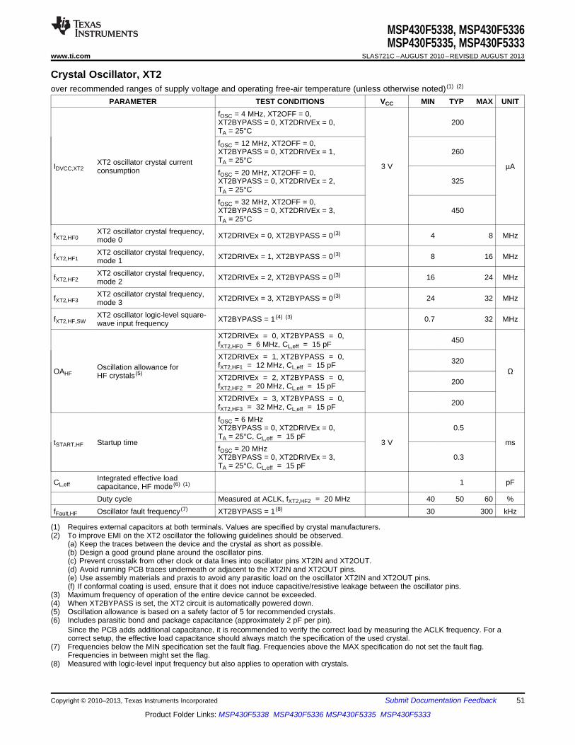
MSP430F5338, MSP430F5336MSP430F5335, MSP430F5333
www.ti.com SLAS721C –AUGUST 2010–REVISED AUGUST 2013
Crystal Oscillator, XT2over recommended ranges of supply voltage and operating free-air temperature (unless otherwise noted) (1) (2)
PARAMETER TEST CONDITIONS VCC MIN TYP MAX UNITfOSC = 4 MHz, XT2OFF = 0,XT2BYPASS = 0, XT2DRIVEx = 0, 200TA = 25°CfOSC = 12 MHz, XT2OFF = 0,XT2BYPASS = 0, XT2DRIVEx = 1, 260TA = 25°CXT2 oscillator crystal currentIDVCC,XT2 3 V µAconsumption fOSC = 20 MHz, XT2OFF = 0,XT2BYPASS = 0, XT2DRIVEx = 2, 325TA = 25°CfOSC = 32 MHz, XT2OFF = 0,XT2BYPASS = 0, XT2DRIVEx = 3, 450TA = 25°C
XT2 oscillator crystal frequency,fXT2,HF0 XT2DRIVEx = 0, XT2BYPASS = 0 (3) 4 8 MHzmode 0XT2 oscillator crystal frequency,fXT2,HF1 XT2DRIVEx = 1, XT2BYPASS = 0 (3) 8 16 MHzmode 1XT2 oscillator crystal frequency,fXT2,HF2 XT2DRIVEx = 2, XT2BYPASS = 0 (3) 16 24 MHzmode 2XT2 oscillator crystal frequency,fXT2,HF3 XT2DRIVEx = 3, XT2BYPASS = 0 (3) 24 32 MHzmode 3XT2 oscillator logic-level square-fXT2,HF,SW XT2BYPASS = 1 (4) (3) 0.7 32 MHzwave input frequency
XT2DRIVEx = 0, XT2BYPASS = 0, 450fXT2,HF0 = 6 MHz, CL,eff = 15 pFXT2DRIVEx = 1, XT2BYPASS = 0, 320fXT2,HF1 = 12 MHz, CL,eff = 15 pFOscillation allowance forOAHF ΩHF crystals (5) XT2DRIVEx = 2, XT2BYPASS = 0, 200fXT2,HF2 = 20 MHz, CL,eff = 15 pFXT2DRIVEx = 3, XT2BYPASS = 0, 200fXT2,HF3 = 32 MHz, CL,eff = 15 pFfOSC = 6 MHzXT2BYPASS = 0, XT2DRIVEx = 0, 0.5TA = 25°C, CL,eff = 15 pF
tSTART,HF Startup time 3 V msfOSC = 20 MHzXT2BYPASS = 0, XT2DRIVEx = 3, 0.3TA = 25°C, CL,eff = 15 pF
Integrated effective loadCL,eff 1 pFcapacitance, HF mode (6) (1)
Duty cycle Measured at ACLK, fXT2,HF2 = 20 MHz 40 50 60 %fFault,HF Oscillator fault frequency (7) XT2BYPASS = 1 (8) 30 300 kHz
(1) Requires external capacitors at both terminals. Values are specified by crystal manufacturers.(2) To improve EMI on the XT2 oscillator the following guidelines should be observed.
(a) Keep the traces between the device and the crystal as short as possible.(b) Design a good ground plane around the oscillator pins.(c) Prevent crosstalk from other clock or data lines into oscillator pins XT2IN and XT2OUT.(d) Avoid running PCB traces underneath or adjacent to the XT2IN and XT2OUT pins.(e) Use assembly materials and praxis to avoid any parasitic load on the oscillator XT2IN and XT2OUT pins.(f) If conformal coating is used, ensure that it does not induce capacitive/resistive leakage between the oscillator pins.
(3) Maximum frequency of operation of the entire device cannot be exceeded.(4) When XT2BYPASS is set, the XT2 circuit is automatically powered down.(5) Oscillation allowance is based on a safety factor of 5 for recommended crystals.(6) Includes parasitic bond and package capacitance (approximately 2 pF per pin).
Since the PCB adds additional capacitance, it is recommended to verify the correct load by measuring the ACLK frequency. For acorrect setup, the effective load capacitance should always match the specification of the used crystal.
(7) Frequencies below the MIN specification set the fault flag. Frequencies above the MAX specification do not set the fault flag.Frequencies in between might set the flag.
(8) Measured with logic-level input frequency but also applies to operation with crystals.
Copyright © 2010–2013, Texas Instruments Incorporated Submit Documentation Feedback 51
Product Folder Links: MSP430F5338 MSP430F5336 MSP430F5335 MSP430F5333
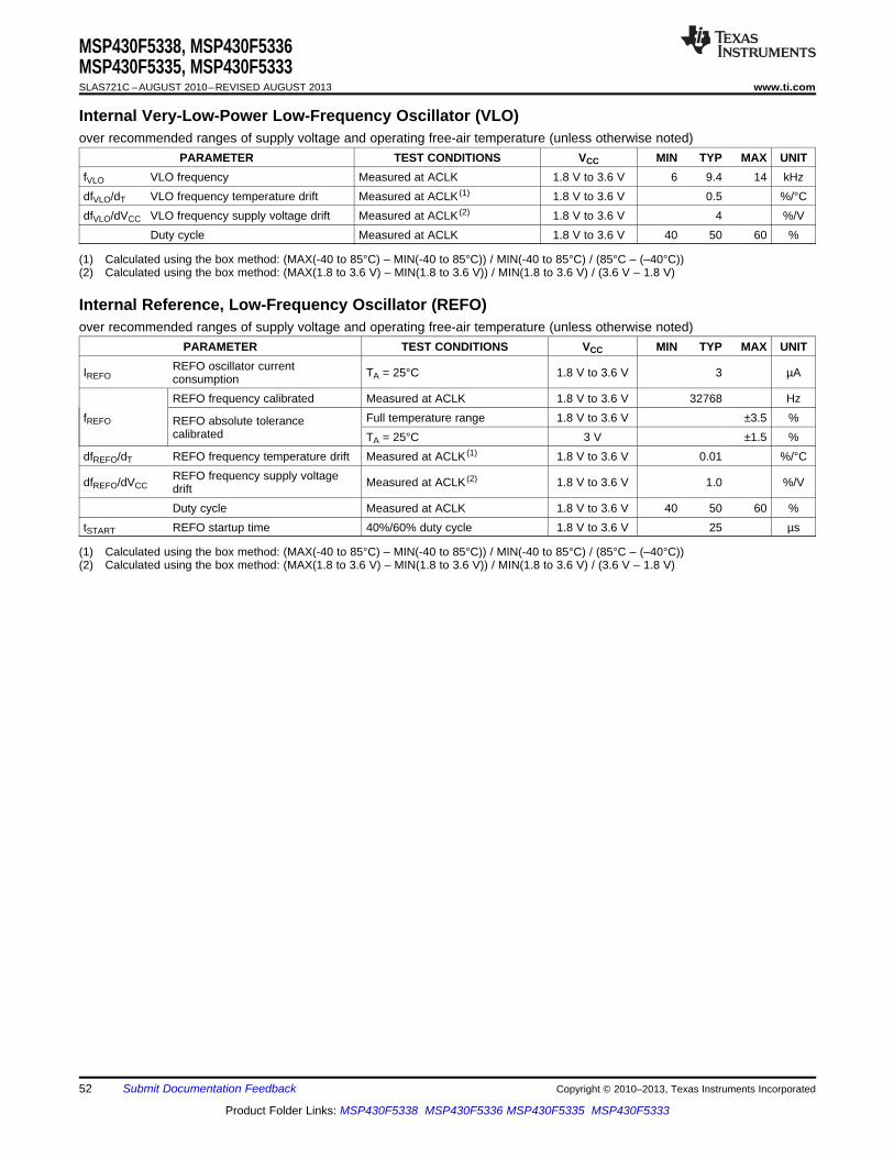
MSP430F5338, MSP430F5336MSP430F5335, MSP430F5333SLAS721C –AUGUST 2010–REVISED AUGUST 2013 www.ti.com
Internal Very-Low-Power Low-Frequency Oscillator (VLO)over recommended ranges of supply voltage and operating free-air temperature (unless otherwise noted)
PARAMETER TEST CONDITIONS VCC MIN TYP MAX UNITfVLO VLO frequency Measured at ACLK 1.8 V to 3.6 V 6 9.4 14 kHzdfVLO/dT VLO frequency temperature drift Measured at ACLK (1) 1.8 V to 3.6 V 0.5 %/°CdfVLO/dVCC VLO frequency supply voltage drift Measured at ACLK (2) 1.8 V to 3.6 V 4 %/V
Duty cycle Measured at ACLK 1.8 V to 3.6 V 40 50 60 %
(1) Calculated using the box method: (MAX(-40 to 85°C) – MIN(-40 to 85°C)) / MIN(-40 to 85°C) / (85°C – (–40°C))(2) Calculated using the box method: (MAX(1.8 to 3.6 V) – MIN(1.8 to 3.6 V)) / MIN(1.8 to 3.6 V) / (3.6 V – 1.8 V)
Internal Reference, Low-Frequency Oscillator (REFO)over recommended ranges of supply voltage and operating free-air temperature (unless otherwise noted)
PARAMETER TEST CONDITIONS VCC MIN TYP MAX UNITREFO oscillator currentIREFO TA = 25°C 1.8 V to 3.6 V 3 µAconsumptionREFO frequency calibrated Measured at ACLK 1.8 V to 3.6 V 32768 Hz
fREFO Full temperature range 1.8 V to 3.6 V ±3.5 %REFO absolute tolerancecalibrated TA = 25°C 3 V ±1.5 %
dfREFO/dT REFO frequency temperature drift Measured at ACLK (1) 1.8 V to 3.6 V 0.01 %/°CREFO frequency supply voltagedfREFO/dVCC Measured at ACLK (2) 1.8 V to 3.6 V 1.0 %/VdriftDuty cycle Measured at ACLK 1.8 V to 3.6 V 40 50 60 %
tSTART REFO startup time 40%/60% duty cycle 1.8 V to 3.6 V 25 µs
(1) Calculated using the box method: (MAX(-40 to 85°C) – MIN(-40 to 85°C)) / MIN(-40 to 85°C) / (85°C – (–40°C))(2) Calculated using the box method: (MAX(1.8 to 3.6 V) – MIN(1.8 to 3.6 V)) / MIN(1.8 to 3.6 V) / (3.6 V – 1.8 V)
52 Submit Documentation Feedback Copyright © 2010–2013, Texas Instruments Incorporated
Product Folder Links: MSP430F5338 MSP430F5336 MSP430F5335 MSP430F5333
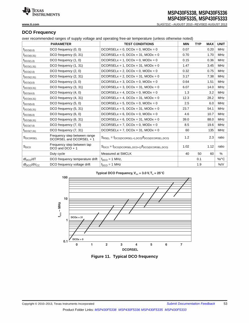
0 1 2 3 4 5 6 7
Typical DCO Frequency, V = 3.0 V,T = 25°CCC A
DCORSEL
100
10
1
0.1
f– M
Hz
DC
O
DCOx = 31
DCOx = 0
MSP430F5338, MSP430F5336MSP430F5335, MSP430F5333
www.ti.com SLAS721C –AUGUST 2010–REVISED AUGUST 2013
DCO Frequencyover recommended ranges of supply voltage and operating free-air temperature (unless otherwise noted)
PARAMETER TEST CONDITIONS MIN TYP MAX UNITfDCO(0,0) DCO frequency (0, 0) DCORSELx = 0, DCOx = 0, MODx = 0 0.07 0.20 MHzfDCO(0,31) DCO frequency (0, 31) DCORSELx = 0, DCOx = 31, MODx = 0 0.70 1.70 MHzfDCO(1,0) DCO frequency (1, 0) DCORSELx = 1, DCOx = 0, MODx = 0 0.15 0.36 MHzfDCO(1,31) DCO frequency (1, 31) DCORSELx = 1, DCOx = 31, MODx = 0 1.47 3.45 MHzfDCO(2,0) DCO frequency (2, 0) DCORSELx = 2, DCOx = 0, MODx = 0 0.32 0.75 MHzfDCO(2,31) DCO frequency (2, 31) DCORSELx = 2, DCOx = 31, MODx = 0 3.17 7.38 MHzfDCO(3,0) DCO frequency (3, 0) DCORSELx = 3, DCOx = 0, MODx = 0 0.64 1.51 MHzfDCO(3,31) DCO frequency (3, 31) DCORSELx = 3, DCOx = 31, MODx = 0 6.07 14.0 MHzfDCO(4,0) DCO frequency (4, 0) DCORSELx = 4, DCOx = 0, MODx = 0 1.3 3.2 MHzfDCO(4,31) DCO frequency (4, 31) DCORSELx = 4, DCOx = 31, MODx = 0 12.3 28.2 MHzfDCO(5,0) DCO frequency (5, 0) DCORSELx = 5, DCOx = 0, MODx = 0 2.5 6.0 MHzfDCO(5,31) DCO frequency (5, 31) DCORSELx = 5, DCOx = 31, MODx = 0 23.7 54.1 MHzfDCO(6,0) DCO frequency (6, 0) DCORSELx = 6, DCOx = 0, MODx = 0 4.6 10.7 MHzfDCO(6,31) DCO frequency (6, 31) DCORSELx = 6, DCOx = 31, MODx = 0 39.0 88.0 MHzfDCO(7,0) DCO frequency (7, 0) DCORSELx = 7, DCOx = 0, MODx = 0 8.5 19.6 MHzfDCO(7,31) DCO frequency (7, 31) DCORSELx = 7, DCOx = 31, MODx = 0 60 135 MHz
Frequency step between rangeSDCORSEL SRSEL = fDCO(DCORSEL+1,DCO)/fDCO(DCORSEL,DCO) 1.2 2.3 ratioDCORSEL and DCORSEL + 1Frequency step between tapSDCO SDCO = fDCO(DCORSEL,DCO+1)/fDCO(DCORSEL,DCO) 1.02 1.12 ratioDCO and DCO + 1Duty cycle Measured at SMCLK 40 50 60 %
dfDCO/dT DCO frequency temperature drift fDCO = 1 MHz, 0.1 %/°CdfDCO/dVCC DCO frequency voltage drift fDCO = 1 MHz 1.9 %/V
Figure 11. Typical DCO frequency
Copyright © 2010–2013, Texas Instruments Incorporated Submit Documentation Feedback 53
Product Folder Links: MSP430F5338 MSP430F5336 MSP430F5335 MSP430F5333
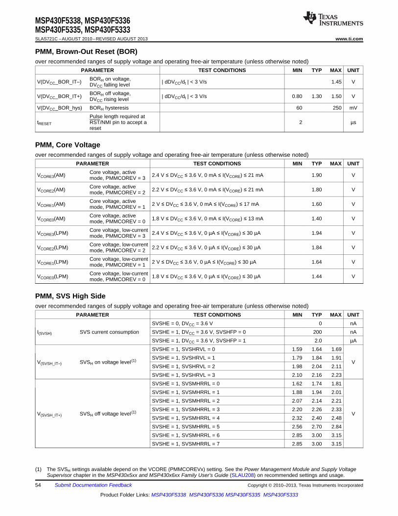
MSP430F5338, MSP430F5336MSP430F5335, MSP430F5333SLAS721C –AUGUST 2010–REVISED AUGUST 2013 www.ti.com
PMM, Brown-Out Reset (BOR)over recommended ranges of supply voltage and operating free-air temperature (unless otherwise noted)
PARAMETER TEST CONDITIONS MIN TYP MAX UNITBORH on voltage,V(DVCC_BOR_IT–) | dDVCC/dt | < 3 V/s 1.45 VDVCC falling levelBORH off voltage,V(DVCC_BOR_IT+) | dDVCC/dt | < 3 V/s 0.80 1.30 1.50 VDVCC rising level
V(DVCC_BOR_hys) BORH hysteresis 60 250 mVPulse length required at
tRESET RST/NMI pin to accept a 2 µsreset
PMM, Core Voltageover recommended ranges of supply voltage and operating free-air temperature (unless otherwise noted)
PARAMETER TEST CONDITIONS MIN TYP MAX UNITCore voltage, activeVCORE3(AM) 2.4 V ≤ DVCC ≤ 3.6 V, 0 mA ≤ I(VCORE) ≤ 21 mA 1.90 Vmode, PMMCOREV = 3Core voltage, activeVCORE2(AM) 2.2 V ≤ DVCC ≤ 3.6 V, 0 mA ≤ I(VCORE) ≤ 21 mA 1.80 Vmode, PMMCOREV = 2Core voltage, activeVCORE1(AM) 2 V ≤ DVCC ≤ 3.6 V, 0 mA ≤ I(VCORE) ≤ 17 mA 1.60 Vmode, PMMCOREV = 1Core voltage, activeVCORE0(AM) 1.8 V ≤ DVCC ≤ 3.6 V, 0 mA ≤ I(VCORE) ≤ 13 mA 1.40 Vmode, PMMCOREV = 0Core voltage, low-currentVCORE3(LPM) 2.4 V ≤ DVCC ≤ 3.6 V, 0 µA ≤ I(VCORE) ≤ 30 µA 1.94 Vmode, PMMCOREV = 3Core voltage, low-currentVCORE2(LPM) 2.2 V ≤ DVCC ≤ 3.6 V, 0 µA ≤ I(VCORE) ≤ 30 µA 1.84 Vmode, PMMCOREV = 2Core voltage, low-currentVCORE1(LPM) 2 V ≤ DVCC ≤ 3.6 V, 0 µA ≤ I(VCORE) ≤ 30 µA 1.64 Vmode, PMMCOREV = 1Core voltage, low-currentVCORE0(LPM) 1.8 V ≤ DVCC ≤ 3.6 V, 0 µA ≤ I(VCORE) ≤ 30 µA 1.44 Vmode, PMMCOREV = 0
PMM, SVS High Sideover recommended ranges of supply voltage and operating free-air temperature (unless otherwise noted)
PARAMETER TEST CONDITIONS MIN TYP MAX UNITSVSHE = 0, DVCC = 3.6 V 0 nA
I(SVSH) SVS current consumption SVSHE = 1, DVCC = 3.6 V, SVSHFP = 0 200 nASVSHE = 1, DVCC = 3.6 V, SVSHFP = 1 2.0 µASVSHE = 1, SVSHRVL = 0 1.59 1.64 1.69SVSHE = 1, SVSHRVL = 1 1.79 1.84 1.91
V(SVSH_IT–) SVSH on voltage level (1) VSVSHE = 1, SVSHRVL = 2 1.98 2.04 2.11SVSHE = 1, SVSHRVL = 3 2.10 2.16 2.23SVSHE = 1, SVSMHRRL = 0 1.62 1.74 1.81SVSHE = 1, SVSMHRRL = 1 1.88 1.94 2.01SVSHE = 1, SVSMHRRL = 2 2.07 2.14 2.21SVSHE = 1, SVSMHRRL = 3 2.20 2.26 2.33
V(SVSH_IT+) SVSH off voltage level (1) VSVSHE = 1, SVSMHRRL = 4 2.32 2.40 2.48SVSHE = 1, SVSMHRRL = 5 2.56 2.70 2.84SVSHE = 1, SVSMHRRL = 6 2.85 3.00 3.15SVSHE = 1, SVSMHRRL = 7 2.85 3.00 3.15
(1) The SVSH settings available depend on the VCORE (PMMCOREVx) setting. See the Power Management Module and Supply VoltageSupervisor chapter in the MSP430x5xx and MSP430x6xx Family User's Guide (SLAU208) on recommended settings and usage.
54 Submit Documentation Feedback Copyright © 2010–2013, Texas Instruments Incorporated
Product Folder Links: MSP430F5338 MSP430F5336 MSP430F5335 MSP430F5333

MSP430F5338, MSP430F5336MSP430F5335, MSP430F5333
www.ti.com SLAS721C –AUGUST 2010–REVISED AUGUST 2013
PMM, SVS High Side (continued)over recommended ranges of supply voltage and operating free-air temperature (unless otherwise noted)
PARAMETER TEST CONDITIONS MIN TYP MAX UNITSVSHE = 1, dVDVCC/dt = 10 mV/µs, SVSHFP = 1 2.5
tpd(SVSH) SVSH propagation delay µsSVSHE = 1, dVDVCC/dt = 1 mV/µs, SVSHFP = 0 20SVSHE = 0→1, SVSHFP = 1 12.5
t(SVSH) SVSH on/off delay time µsSVSHE = 0→1, SVSHFP = 0 100
dVDVCC/dt DVCC rise time 0 1000 V/s
PMM, SVM High Sideover recommended ranges of supply voltage and operating free-air temperature (unless otherwise noted)
PARAMETER TEST CONDITIONS MIN TYP MAX UNITSVMHE = 0, DVCC = 3.6 V 0 nA
I(SVMH) SVMH current consumption SVMHE = 1, DVCC = 3.6 V, SVMHFP = 0 200 nASVMHE = 1, DVCC = 3.6 V, SVMHFP = 1 2.0 µASVMHE = 1, SVSMHRRL = 0 1.65 1.74 1.86SVMHE = 1, SVSMHRRL = 1 1.85 1.94 2.02SVMHE = 1, SVSMHRRL = 2 2.02 2.14 2.22SVMHE = 1, SVSMHRRL = 3 2.18 2.26 2.35
V(SVMH) SVMH on or off voltage level (1) SVMHE = 1, SVSMHRRL = 4 2.32 2.40 2.48 VSVMHE = 1, SVSMHRRL = 5 2.56 2.70 2.84SVMHE = 1, SVSMHRRL = 6 2.85 3.00 3.15SVMHE = 1, SVSMHRRL = 7 2.85 3.00 3.15SVMHE = 1, SVMHOVPE = 1 3.75SVMHE = 1, dVDVCC/dt = 10 mV/µs, SVMHFP = 1 2.5 µs
tpd(SVMH) SVMH propagation delaySVMHE = 1, dVDVCC/dt = 1 mV/µs, SVMHFP = 0 20 µsSVMHE = 0→1, SVSMFP = 1 12.5 µs
t(SVMH) SVMH on or off delay timeSVMHE = 0→1, SVMHFP = 0 100 µs
(1) The SVMH settings available depend on the VCORE (PMMCOREVx) setting. See the Power Management Module and Supply VoltageSupervisor chapter in the MSP430x5xx and MSP430x6xx Family User's Guide (SLAU208) on recommended settings and usage.
PMM, SVS Low Sideover recommended ranges of supply voltage and operating free-air temperature (unless otherwise noted)
PARAMETER TEST CONDITIONS MIN TYP MAX UNITSVSLE = 0, PMMCOREV = 2 0 nA
I(SVSL) SVSL current consumption SVSLE = 1, PMMCOREV = 2, SVSLFP = 0 200 nASVSLE = 1, PMMCOREV = 2, SVSLFP = 1 2.0 µASVSLE = 1, dVCORE/dt = 10 mV/µs, SVSLFP = 1 2.5
tpd(SVSL) SVSL propagation delay µsSVSLE = 1, dVCORE/dt = 1 mV/µs, SVSLFP = 0 20SVSLE = 0→1, SVSLFP = 1 12.5
t(SVSL) SVSL on/off delay time µsSVSLE = 0→1, SVSLFP = 0 100
PMM, SVM Low Sideover recommended ranges of supply voltage and operating free-air temperature (unless otherwise noted)
PARAMETER TEST CONDITIONS MIN TYP MAX UNITSVMLE = 0, PMMCOREV = 2 0 nA
I(SVML) SVML current consumption SVMLE = 1, PMMCOREV = 2, SVMLFP = 0 200 nASVMLE = 1, PMMCOREV = 2, SVMLFP = 1 2.0 µA
Copyright © 2010–2013, Texas Instruments Incorporated Submit Documentation Feedback 55
Product Folder Links: MSP430F5338 MSP430F5336 MSP430F5335 MSP430F5333
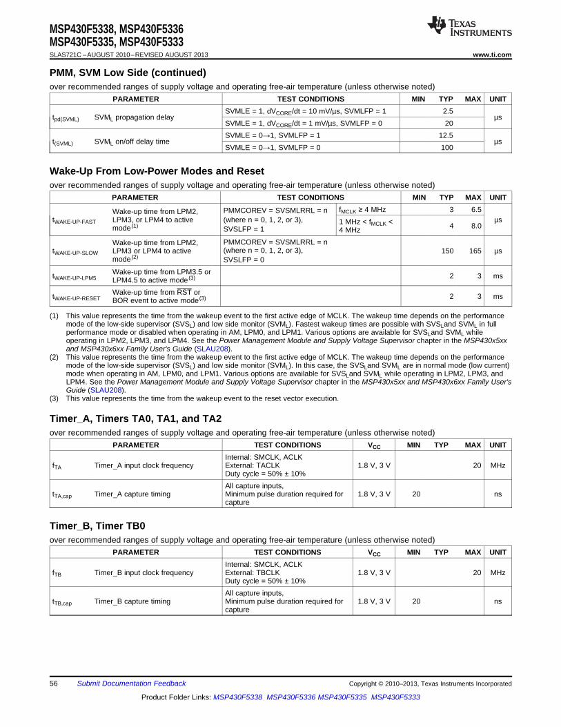
MSP430F5338, MSP430F5336MSP430F5335, MSP430F5333SLAS721C –AUGUST 2010–REVISED AUGUST 2013 www.ti.com
PMM, SVM Low Side (continued)over recommended ranges of supply voltage and operating free-air temperature (unless otherwise noted)
PARAMETER TEST CONDITIONS MIN TYP MAX UNITSVMLE = 1, dVCORE/dt = 10 mV/µs, SVMLFP = 1 2.5
tpd(SVML) SVML propagation delay µsSVMLE = 1, dVCORE/dt = 1 mV/µs, SVMLFP = 0 20SVMLE = 0→1, SVMLFP = 1 12.5
t(SVML) SVML on/off delay time µsSVMLE = 0→1, SVMLFP = 0 100
Wake-Up From Low-Power Modes and Resetover recommended ranges of supply voltage and operating free-air temperature (unless otherwise noted)
PARAMETER TEST CONDITIONS MIN TYP MAX UNITfMCLK ≥ 4 MHz 3 6.5PMMCOREV = SVSMLRRL = nWake-up time from LPM2,
tWAKE-UP-FAST LPM3, or LPM4 to active (where n = 0, 1, 2, or 3), µs1 MHz < fMCLK < 4 8.0mode (1) SVSLFP = 1 4 MHzPMMCOREV = SVSMLRRL = nWake-up time from LPM2,(where n = 0, 1, 2, or 3),tWAKE-UP-SLOW LPM3 or LPM4 to active 150 165 µs
mode (2) SVSLFP = 0Wake-up time from LPM3.5 ortWAKE-UP-LPM5 2 3 msLPM4.5 to active mode (3)
Wake-up time from RST ortWAKE-UP-RESET 2 3 msBOR event to active mode (3)
(1) This value represents the time from the wakeup event to the first active edge of MCLK. The wakeup time depends on the performancemode of the low-side supervisor (SVSL) and low side monitor (SVML). Fastest wakeup times are possible with SVSLand SVML in fullperformance mode or disabled when operating in AM, LPM0, and LPM1. Various options are available for SVSLand SVML whileoperating in LPM2, LPM3, and LPM4. See the Power Management Module and Supply Voltage Supervisor chapter in the MSP430x5xxand MSP430x6xx Family User's Guide (SLAU208).
(2) This value represents the time from the wakeup event to the first active edge of MCLK. The wakeup time depends on the performancemode of the low-side supervisor (SVSL) and low side monitor (SVML). In this case, the SVSLand SVML are in normal mode (low current)mode when operating in AM, LPM0, and LPM1. Various options are available for SVSLand SVML while operating in LPM2, LPM3, andLPM4. See the Power Management Module and Supply Voltage Supervisor chapter in the MSP430x5xx and MSP430x6xx Family User'sGuide (SLAU208).
(3) This value represents the time from the wakeup event to the reset vector execution.
Timer_A, Timers TA0, TA1, and TA2over recommended ranges of supply voltage and operating free-air temperature (unless otherwise noted)
PARAMETER TEST CONDITIONS VCC MIN TYP MAX UNITInternal: SMCLK, ACLK
fTA Timer_A input clock frequency External: TACLK 1.8 V, 3 V 20 MHzDuty cycle = 50% ± 10%All capture inputs,
tTA,cap Timer_A capture timing Minimum pulse duration required for 1.8 V, 3 V 20 nscapture
Timer_B, Timer TB0over recommended ranges of supply voltage and operating free-air temperature (unless otherwise noted)
PARAMETER TEST CONDITIONS VCC MIN TYP MAX UNITInternal: SMCLK, ACLK
fTB Timer_B input clock frequency External: TBCLK 1.8 V, 3 V 20 MHzDuty cycle = 50% ± 10%All capture inputs,
tTB,cap Timer_B capture timing Minimum pulse duration required for 1.8 V, 3 V 20 nscapture
56 Submit Documentation Feedback Copyright © 2010–2013, Texas Instruments Incorporated
Product Folder Links: MSP430F5338 MSP430F5336 MSP430F5335 MSP430F5333
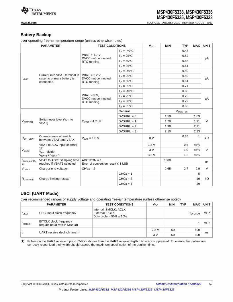
MSP430F5338, MSP430F5336MSP430F5335, MSP430F5333
www.ti.com SLAS721C –AUGUST 2010–REVISED AUGUST 2013
Battery Backupover operating free-air temperature range (unless otherwise noted)
PARAMETER TEST CONDITIONS VCC MIN TYP MAX UNITTA = -40°C 0.43
VBAT = 1.7 V, TA = 25°C 0.52DVCC not connected, µA
TA = 60°C 0.58RTC runningTA = 85°C 0.64TA = -40°C 0.50
Current into VBAT terminal in VBAT = 2.2 V, TA = 25°C 0.59IVBAT case no primary battery is DVCC not connected, µA
TA = 60°C 0.64connected. RTC runningTA = 85°C 0.71TA = -40°C 0.68
VBAT = 3 V, TA = 25°C 0.75DVCC not connected, µA
TA = 60°C 0.79RTC runningTA = 85°C 0.86General VSVSH_IT-
SVSHRL = 0 1.59 1.69Switch-over level (VCC toVSWITCH CVCC = 4.7 µF SVSHRL = 1 1.79 1.91 VVBAT)
SVSHRL = 2 1.98 2.11SVSHRL = 3 2.10 2.23
On-resistance of switch 0.35 1RON_VBAT VBAT = 1.8 V 0 V kΩbetween VBAT and VBAKVBAT to ADC input channel 1.8 V 0.6 ±5%12: 3 V 1.0 ±5%VBAT3 VVBAT divide,
1.2 ±5%3.6 VVBAT3 ≠ VBAT /3tSample,VBA VBAT to ADC: Sampling time ADC12ON = 1, 1000 nsT3 required if VBAT3 selected Error of conversion result ≤ 1 LSBVCHVx Charger end voltage CHVx = 2 2.65 2.7 2.9 V
CHCx = 1 5RCHARGE Charge limiting resistor CHCx = 2 10 kΩ
CHCx = 3 20
USCI (UART Mode)over recommended ranges of supply voltage and operating free-air temperature (unless otherwise noted)
PARAMETER TEST CONDITIONS VCC MIN TYP MAX UNITInternal: SMCLK, ACLK
fUSCI USCI input clock frequency External: UCLK fSYSTEM MHzDuty cycle = 50% ± 10%
BITCLK clock frequencyfBITCLK 1 MHz(equals baud rate in MBaud)2.2 V 50 600
tτ UART receive deglitch time (1) ns3 V 50 600
(1) Pulses on the UART receive input (UCxRX) shorter than the UART receive deglitch time are suppressed. To ensure that pulses arecorrectly recognized their width should exceed the maximum specification of the deglitch time.
Copyright © 2010–2013, Texas Instruments Incorporated Submit Documentation Feedback 57
Product Folder Links: MSP430F5338 MSP430F5336 MSP430F5335 MSP430F5333

tSU,MI
tHD,MI
UCLK
SOMI
SIMO
tVALID,MO
tHD,MO
CKPL = 0
CKPL = 1
tLO/HI tLO/HI
1/fUCxCLK
MSP430F5338, MSP430F5336MSP430F5335, MSP430F5333SLAS721C –AUGUST 2010–REVISED AUGUST 2013 www.ti.com
USCI (SPI Master Mode)over recommended ranges of supply voltage and operating free-air temperature (unless otherwise noted) (1)
(see Figure 12 and )PARAMETER TEST CONDITIONS VCC MIN TYP MAX UNIT
SMCLK, ACLK,fUSCI USCI input clock frequency fSYSTEM MHzDuty cycle = 50% ± 10%1.8 V 55
PMMCOREV = 0 ns3 V 38
tSU,MI SOMI input data setup time2.4 V 30
PMMCOREV = 3 ns3 V 25
1.8 V 0PMMCOREV = 0 ns
3 V 0tHD,MI SOMI input data hold time
2.4 V 0PMMCOREV = 3 ns
3 V 0UCLK edge to SIMO valid, 1.8 V 20CL = 20 pF, ns
3 V 18PMMCOREV = 0tVALID,MO SIMO output data valid time (2)
2.4 V 16UCLK edge to SIMO valid, nsCL = 20 pF, PMMCOREV = 3 3 V 151.8 V -10
CL = 20 pF, PMMCOREV = 0 ns3 V -8
tHD,MO SIMO output data hold time (3)2.4 V -10
CL = 20 pF, PMMCOREV = 3 ns3 V -8
(1) fUCxCLK = 1/2tLO/HI with tLO/HI ≥ max(tVALID,MO(USCI) + tSU,SI(Slave), tSU,MI(USCI) + tVALID,SO(Slave)).For the slave's parameters tSU,SI(Slave) and tVALID,SO(Slave), see the SPI parameters of the attached slave.
(2) Specifies the time to drive the next valid data to the SIMO output after the output changing UCLK clock edge. See the timing diagramsin Figure 12 and .
(3) Specifies how long data on the SIMO output is valid after the output changing UCLK clock edge. Negative values indicate that the dataon the SIMO output can become invalid before the output changing clock edge observed on UCLK. See the timing diagrams inFigure 12 and .
Figure 12. SPI Master Mode, CKPH = 0
58 Submit Documentation Feedback Copyright © 2010–2013, Texas Instruments Incorporated
Product Folder Links: MSP430F5338 MSP430F5336 MSP430F5335 MSP430F5333
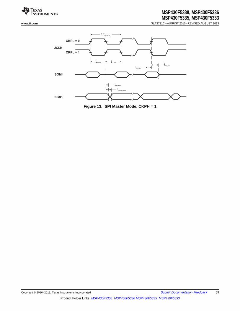
tSU,MI
tHD,MI
UCLK
SOMI
SIMO
tVALID,MO
CKPL = 0
CKPL = 1
1/fUCxCLK
tHD,MO
tLO/HI tLO/HI
MSP430F5338, MSP430F5336MSP430F5335, MSP430F5333
www.ti.com SLAS721C –AUGUST 2010–REVISED AUGUST 2013
Figure 13. SPI Master Mode, CKPH = 1
Copyright © 2010–2013, Texas Instruments Incorporated Submit Documentation Feedback 59
Product Folder Links: MSP430F5338 MSP430F5336 MSP430F5335 MSP430F5333

MSP430F5338, MSP430F5336MSP430F5335, MSP430F5333SLAS721C –AUGUST 2010–REVISED AUGUST 2013 www.ti.com
USCI (SPI Slave Mode)over recommended ranges of supply voltage and operating free-air temperature (unless otherwise noted) (1)
(see Figure 14 and Figure 15)PARAMETER TEST CONDITIONS VCC MIN TYP MAX UNIT
1.8 V 11PMMCOREV = 0 ns
3 V 8tSTE,LEAD STE lead time, STE low to clock
2.4 V 7PMMCOREV = 3 ns
3 V 61.8 V 3
PMMCOREV = 0 ns3 V 3
tSTE,LAG STE lag time, Last clock to STE high2.4 V 3
PMMCOREV = 3 ns3 V 3
1.8 V 66PMMCOREV = 0 ns
3 V 50tSTE,ACC STE access time, STE low to SOMI data out
2.4 V 36PMMCOREV = 3 ns
3 V 301.8 V 30
PMMCOREV = 0 ns3 V 23STE disable time, STE high to SOMI hightSTE,DIS impedance 2.4 V 16
PMMCOREV = 3 ns3 V 13
1.8 V 5PMMCOREV = 0 ns
3 V 5tSU,SI SIMO input data setup time
2.4 V 2PMMCOREV = 3 ns
3 V 21.8 V 5
PMMCOREV = 0 ns3 V 5
tHD,SI SIMO input data hold time2.4 V 5
PMMCOREV = 3 ns3 V 5
UCLK edge to SOMI valid, 1.8 V 76CL = 20 pF, ns
3 V 60PMMCOREV = 0tVALID,SO SOMI output data valid time (2)
UCLK edge to SOMI valid, 2.4 V 44CL = 20 pF, ns
3 V 40PMMCOREV = 31.8 V 18CL = 20 pF, nsPMMCOREV = 0 3 V 12
tHD,SO SOMI output data hold time (3)2.4 V 10CL = 20 pF, nsPMMCOREV = 3 3 V 8
(1) fUCxCLK = 1/2tLO/HI with tLO/HI ≥ max(tVALID,MO(Master) + tSU,SI(USCI), tSU,MI(Master) + tVALID,SO(USCI)).For the master's parameters tSU,MI(Master) and tVALID,MO(Master), see the SPI parameters of the attached slave.
(2) Specifies the time to drive the next valid data to the SOMI output after the output changing UCLK clock edge. See the timing diagramsin Figure 14 and Figure 15.
(3) Specifies how long data on the SOMI output is valid after the output changing UCLK clock edge. See the timing diagrams in Figure 14and Figure 15.
60 Submit Documentation Feedback Copyright © 2010–2013, Texas Instruments Incorporated
Product Folder Links: MSP430F5338 MSP430F5336 MSP430F5335 MSP430F5333
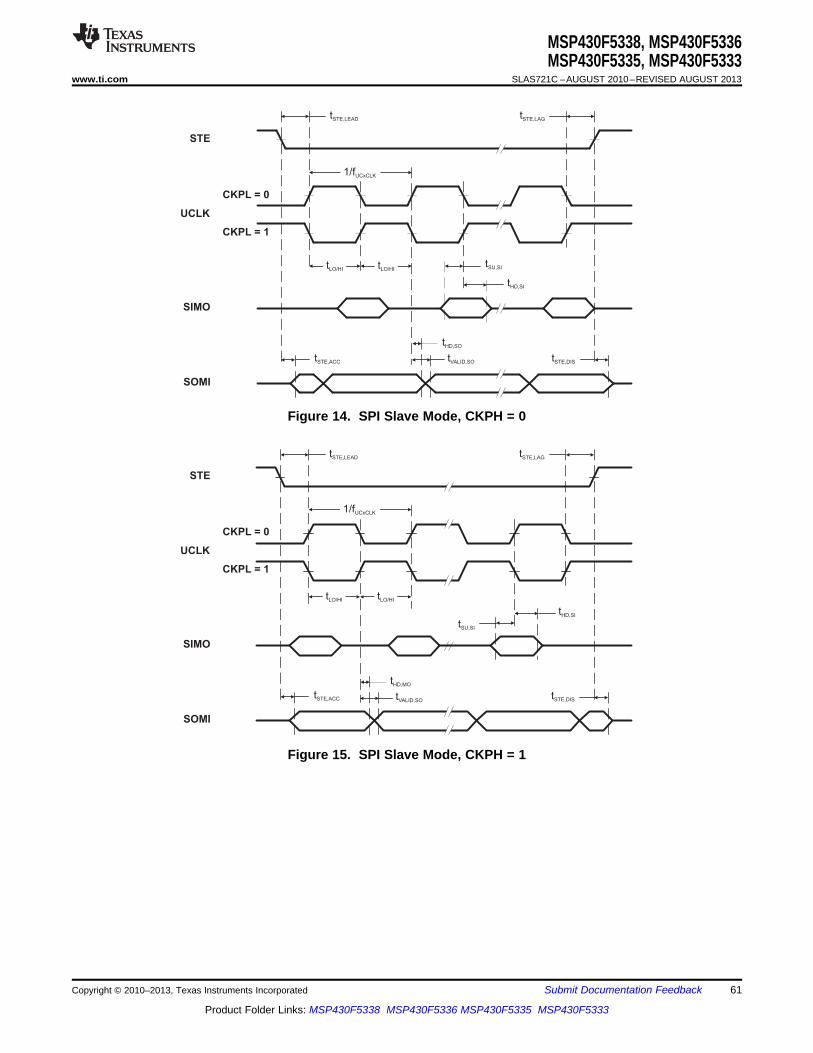
STE
UCLK
CKPL = 0
CKPL = 1
SOMI
SIMO
tSU,SI
tHD,SI
tVALID,SO
tSTE,LEAD
1/fUCxCLK
tSTE,LAG
tSTE,DIStSTE,ACC
tHD,MO
tLO/HI tLO/HI
STE
UCLK
CKPL = 0
CKPL = 1
SOMI
SIMO
tSU,SI
tHD,SI
tVALID,SO
tSTE,LEAD
1/fUCxCLK
tLO/HI tLO/HI
tSTE,LAG
tSTE,DIStSTE,ACC
tHD,SO
MSP430F5338, MSP430F5336MSP430F5335, MSP430F5333
www.ti.com SLAS721C –AUGUST 2010–REVISED AUGUST 2013
Figure 14. SPI Slave Mode, CKPH = 0
Figure 15. SPI Slave Mode, CKPH = 1
Copyright © 2010–2013, Texas Instruments Incorporated Submit Documentation Feedback 61
Product Folder Links: MSP430F5338 MSP430F5336 MSP430F5335 MSP430F5333
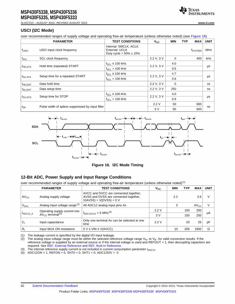
SDA
SCL
tHD,DAT
tSU,DAT
tHD,STA
tHIGHtLOW
tBUFtHD,STAtSU,STA
tSP
tSU,STO
MSP430F5338, MSP430F5336MSP430F5335, MSP430F5333SLAS721C –AUGUST 2010–REVISED AUGUST 2013 www.ti.com
USCI (I2C Mode)over recommended ranges of supply voltage and operating free-air temperature (unless otherwise noted) (see Figure 16)
PARAMETER TEST CONDITIONS VCC MIN TYP MAX UNITInternal: SMCLK, ACLK
fUSCI USCI input clock frequency External: UCLK fSYSTEM MHzDuty cycle = 50% ± 10%
fSCL SCL clock frequency 2.2 V, 3 V 0 400 kHzfSCL ≤ 100 kHz 4.0
tHD,STA Hold time (repeated) START 2.2 V, 3 V µsfSCL > 100 kHz 0.6fSCL ≤ 100 kHz 4.7
tSU,STA Setup time for a repeated START 2.2 V, 3 V µsfSCL > 100 kHz 0.6
tHD,DAT Data hold time 2.2 V, 3 V 0 nstSU,DAT Data setup time 2.2 V, 3 V 250 ns
fSCL ≤ 100 kHz 4.0tSU,STO Setup time for STOP 2.2 V, 3 V µs
fSCL > 100 kHz 0.62.2 V 50 600
tSP Pulse width of spikes suppressed by input filter ns3 V 50 600
Figure 16. I2C Mode Timing
12-Bit ADC, Power Supply and Input Range Conditionsover recommended ranges of supply voltage and operating free-air temperature (unless otherwise noted) (1)
PARAMETER TEST CONDITIONS VCC MIN TYP MAX UNITAVCC and DVCC are connected together,
AVCC Analog supply voltage AVSS and DVSS are connected together, 2.2 3.6 VV(AVSS) = V(DVSS) = 0 V
V(Ax) Analog input voltage range (2) All ADC12 analog input pins Ax 0 AVCC V2.2 V 150 200Operating supply current intoIADC12_A fADC12CLK = 5 MHz (4) µAAVCC terminal (3) 3 V 150 250
Only one terminal Ax can be selected at oneCI Input capacitance 2.2 V 20 25 pFtimeRI Input MUX ON resistance 0 V ≤ VIN ≤ V(AVCC) 10 200 1900 Ω
(1) The leakage current is specified by the digital I/O input leakage.(2) The analog input voltage range must be within the selected reference voltage range VR+ to VR– for valid conversion results. If the
reference voltage is supplied by an external source or if the internal voltage is used and REFOUT = 1, then decoupling capacitors arerequired. See REF, External Reference and REF, Built-In Reference.
(3) The internal reference supply current is not included in current consumption parameter IADC12.(4) ADC12ON = 1, REFON = 0, SHT0 = 0, SHT1 = 0, ADC12DIV = 0
62 Submit Documentation Feedback Copyright © 2010–2013, Texas Instruments Incorporated
Product Folder Links: MSP430F5338 MSP430F5336 MSP430F5335 MSP430F5333
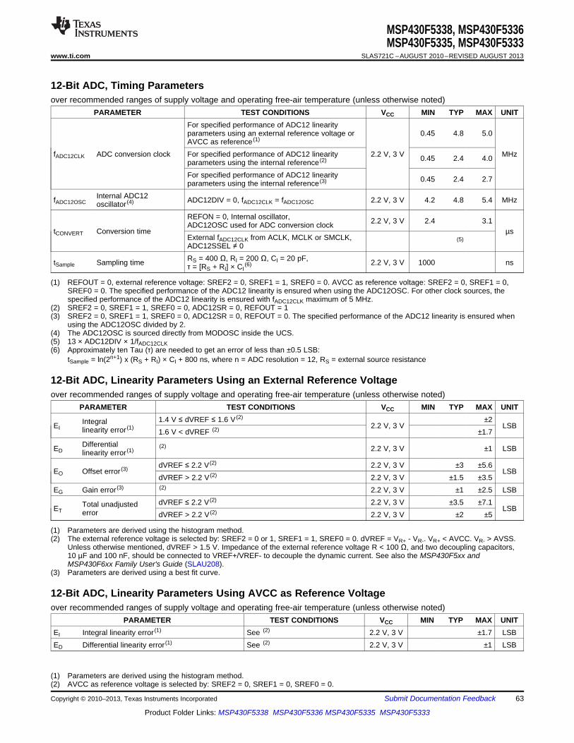
MSP430F5338, MSP430F5336MSP430F5335, MSP430F5333
www.ti.com SLAS721C –AUGUST 2010–REVISED AUGUST 2013
12-Bit ADC, Timing Parametersover recommended ranges of supply voltage and operating free-air temperature (unless otherwise noted)
PARAMETER TEST CONDITIONS VCC MIN TYP MAX UNITFor specified performance of ADC12 linearityparameters using an external reference voltage or 0.45 4.8 5.0AVCC as reference (1)
fADC12CLK ADC conversion clock For specified performance of ADC12 linearity 2.2 V, 3 V MHz0.45 2.4 4.0parameters using the internal reference (2)
For specified performance of ADC12 linearity 0.45 2.4 2.7parameters using the internal reference (3)
Internal ADC12fADC12OSC ADC12DIV = 0, fADC12CLK = fADC12OSC 2.2 V, 3 V 4.2 4.8 5.4 MHzoscillator (4)
REFON = 0, Internal oscillator, 2.2 V, 3 V 2.4 3.1ADC12OSC used for ADC conversion clocktCONVERT Conversion time µs
External fADC12CLK from ACLK, MCLK or SMCLK, (5)ADC12SSEL ≠ 0RS = 400 Ω, RI = 200 Ω, CI = 20 pF,tSample Sampling time 2.2 V, 3 V 1000 nsτ = [RS + RI] × CI
(6)
(1) REFOUT = 0, external reference voltage: SREF2 = 0, SREF1 = 1, SREF0 = 0. AVCC as reference voltage: SREF2 = 0, SREF1 = 0,SREF0 = 0. The specified performance of the ADC12 linearity is ensured when using the ADC12OSC. For other clock sources, thespecified performance of the ADC12 linearity is ensured with fADC12CLK maximum of 5 MHz.
(2) SREF2 = 0, SREF1 = 1, SREF0 = 0, ADC12SR = 0, REFOUT = 1(3) SREF2 = 0, SREF1 = 1, SREF0 = 0, ADC12SR = 0, REFOUT = 0. The specified performance of the ADC12 linearity is ensured when
using the ADC12OSC divided by 2.(4) The ADC12OSC is sourced directly from MODOSC inside the UCS.(5) 13 × ADC12DIV × 1/fADC12CLK(6) Approximately ten Tau (τ) are needed to get an error of less than ±0.5 LSB:
tSample = ln(2n+1) x (RS + RI) × CI + 800 ns, where n = ADC resolution = 12, RS = external source resistance
12-Bit ADC, Linearity Parameters Using an External Reference Voltageover recommended ranges of supply voltage and operating free-air temperature (unless otherwise noted)
PARAMETER TEST CONDITIONS VCC MIN TYP MAX UNIT1.4 V ≤ dVREF ≤ 1.6 V (2) ±2IntegralEI 2.2 V, 3 V LSBlinearity error (1) 1.6 V < dVREF (2) ±1.7
DifferentialED(2) 2.2 V, 3 V ±1 LSBlinearity error (1)
dVREF ≤ 2.2 V (2) 2.2 V, 3 V ±3 ±5.6EO Offset error (3) LSB
dVREF > 2.2 V (2) 2.2 V, 3 V ±1.5 ±3.5EG Gain error (3) (2) 2.2 V, 3 V ±1 ±2.5 LSB
dVREF ≤ 2.2 V (2) 2.2 V, 3 V ±3.5 ±7.1Total unadjustedET LSBerror dVREF > 2.2 V (2) 2.2 V, 3 V ±2 ±5
(1) Parameters are derived using the histogram method.(2) The external reference voltage is selected by: SREF2 = 0 or 1, SREF1 = 1, SREF0 = 0. dVREF = VR+ - VR-. VR+ < AVCC. VR- > AVSS.
Unless otherwise mentioned, dVREF > 1.5 V. Impedance of the external reference voltage R < 100 Ω, and two decoupling capacitors,10 µF and 100 nF, should be connected to VREF+/VREF- to decouple the dynamic current. See also the MSP430F5xx andMSP430F6xx Family User's Guide (SLAU208).
(3) Parameters are derived using a best fit curve.
12-Bit ADC, Linearity Parameters Using AVCC as Reference Voltageover recommended ranges of supply voltage and operating free-air temperature (unless otherwise noted)
PARAMETER TEST CONDITIONS VCC MIN TYP MAX UNITEI Integral linearity error (1) See (2) 2.2 V, 3 V ±1.7 LSBED Differential linearity error (1) See (2) 2.2 V, 3 V ±1 LSB
(1) Parameters are derived using the histogram method.(2) AVCC as reference voltage is selected by: SREF2 = 0, SREF1 = 0, SREF0 = 0.
Copyright © 2010–2013, Texas Instruments Incorporated Submit Documentation Feedback 63
Product Folder Links: MSP430F5338 MSP430F5336 MSP430F5335 MSP430F5333
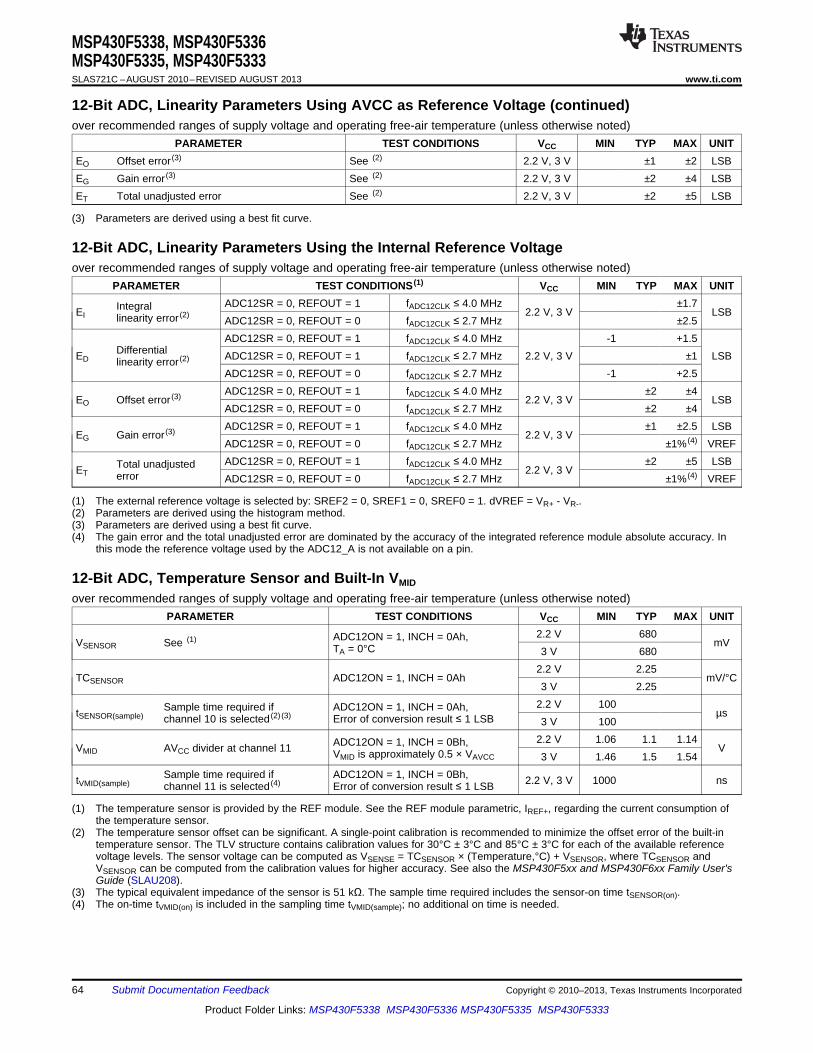
MSP430F5338, MSP430F5336MSP430F5335, MSP430F5333SLAS721C –AUGUST 2010–REVISED AUGUST 2013 www.ti.com
12-Bit ADC, Linearity Parameters Using AVCC as Reference Voltage (continued)over recommended ranges of supply voltage and operating free-air temperature (unless otherwise noted)
PARAMETER TEST CONDITIONS VCC MIN TYP MAX UNITEO Offset error (3) See (2) 2.2 V, 3 V ±1 ±2 LSBEG Gain error (3) See (2) 2.2 V, 3 V ±2 ±4 LSBET Total unadjusted error See (2) 2.2 V, 3 V ±2 ±5 LSB
(3) Parameters are derived using a best fit curve.
12-Bit ADC, Linearity Parameters Using the Internal Reference Voltageover recommended ranges of supply voltage and operating free-air temperature (unless otherwise noted)
PARAMETER TEST CONDITIONS (1) VCC MIN TYP MAX UNITADC12SR = 0, REFOUT = 1 fADC12CLK ≤ 4.0 MHz ±1.7IntegralEI 2.2 V, 3 V LSBlinearity error (2) ADC12SR = 0, REFOUT = 0 fADC12CLK ≤ 2.7 MHz ±2.5ADC12SR = 0, REFOUT = 1 fADC12CLK ≤ 4.0 MHz -1 +1.5
DifferentialED ADC12SR = 0, REFOUT = 1 fADC12CLK ≤ 2.7 MHz 2.2 V, 3 V ±1 LSBlinearity error (2)
ADC12SR = 0, REFOUT = 0 fADC12CLK ≤ 2.7 MHz -1 +2.5ADC12SR = 0, REFOUT = 1 fADC12CLK ≤ 4.0 MHz ±2 ±4
EO Offset error (3) 2.2 V, 3 V LSBADC12SR = 0, REFOUT = 0 fADC12CLK ≤ 2.7 MHz ±2 ±4ADC12SR = 0, REFOUT = 1 fADC12CLK ≤ 4.0 MHz ±1 ±2.5 LSB
EG Gain error (3) 2.2 V, 3 VADC12SR = 0, REFOUT = 0 fADC12CLK ≤ 2.7 MHz ±1% (4) VREFADC12SR = 0, REFOUT = 1 fADC12CLK ≤ 4.0 MHz ±2 ±5 LSBTotal unadjustedET 2.2 V, 3 Verror ADC12SR = 0, REFOUT = 0 fADC12CLK ≤ 2.7 MHz ±1% (4) VREF
(1) The external reference voltage is selected by: SREF2 = 0, SREF1 = 0, SREF0 = 1. dVREF = VR+ - VR-.(2) Parameters are derived using the histogram method.(3) Parameters are derived using a best fit curve.(4) The gain error and the total unadjusted error are dominated by the accuracy of the integrated reference module absolute accuracy. In
this mode the reference voltage used by the ADC12_A is not available on a pin.
12-Bit ADC, Temperature Sensor and Built-In VMID
over recommended ranges of supply voltage and operating free-air temperature (unless otherwise noted)PARAMETER TEST CONDITIONS VCC MIN TYP MAX UNIT
2.2 V 680ADC12ON = 1, INCH = 0Ah,VSENSOR See (1) mVTA = 0°C 3 V 6802.2 V 2.25
TCSENSOR ADC12ON = 1, INCH = 0Ah mV/°C3 V 2.25
2.2 V 100Sample time required if ADC12ON = 1, INCH = 0Ah,tSENSOR(sample) µschannel 10 is selected (2) (3) Error of conversion result ≤ 1 LSB 3 V 1002.2 V 1.06 1.1 1.14ADC12ON = 1, INCH = 0Bh,VMID AVCC divider at channel 11 VVMID is approximately 0.5 × VAVCC 3 V 1.46 1.5 1.54
Sample time required if ADC12ON = 1, INCH = 0Bh,tVMID(sample) 2.2 V, 3 V 1000 nschannel 11 is selected (4) Error of conversion result ≤ 1 LSB
(1) The temperature sensor is provided by the REF module. See the REF module parametric, IREF+, regarding the current consumption ofthe temperature sensor.
(2) The temperature sensor offset can be significant. A single-point calibration is recommended to minimize the offset error of the built-intemperature sensor. The TLV structure contains calibration values for 30°C ± 3°C and 85°C ± 3°C for each of the available referencevoltage levels. The sensor voltage can be computed as VSENSE = TCSENSOR × (Temperature,°C) + VSENSOR, where TCSENSOR andVSENSOR can be computed from the calibration values for higher accuracy. See also the MSP430F5xx and MSP430F6xx Family User'sGuide (SLAU208).
(3) The typical equivalent impedance of the sensor is 51 kΩ. The sample time required includes the sensor-on time tSENSOR(on).(4) The on-time tVMID(on) is included in the sampling time tVMID(sample); no additional on time is needed.
64 Submit Documentation Feedback Copyright © 2010–2013, Texas Instruments Incorporated
Product Folder Links: MSP430F5338 MSP430F5336 MSP430F5335 MSP430F5333
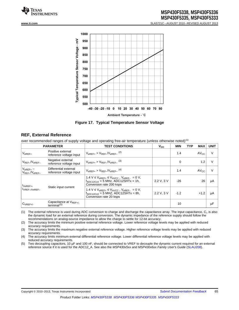
500
550
600
650
700
750
800
850
900
950
1000
-40 -30 -20 -10 0 10 20 30 40 50 60 70 80
Typ
icalT
em
pera
ture
Sen
so
rV
olt
ag
e-
mV
Ambient Temperature - ˚C
MSP430F5338, MSP430F5336MSP430F5335, MSP430F5333
www.ti.com SLAS721C –AUGUST 2010–REVISED AUGUST 2013
Figure 17. Typical Temperature Sensor Voltage
REF, External Referenceover recommended ranges of supply voltage and operating free-air temperature (unless otherwise noted) (1)
PARAMETER TEST CONDITIONS VCC MIN TYP MAX UNITPositive externalVeREF+ VeREF+ > VREF–/VeREF–
(2) 1.4 AVCC Vreference voltage inputNegative externalVREF–/VeREF– VeREF+ > VREF–/VeREF–
(3) 0 1.2 Vreference voltage inputVeREF+ – Differential external VeREF+ > VREF–/VeREF–
(4) 1.4 AVCC VVREF–/VeREF– reference voltage input1.4 V ≤ VeREF+ ≤ VAVCC , VeREF– = 0 V,fADC12CLK = 5 MHz, ADC12SHTx = 1h, 2.2 V, 3 V -26 26 µAConversion rate 200 kspsIVeREF+, Static input currentIVREF–/VeREF– 1.4 V ≤ VeREF+ ≤ VAVCC , VeREF– = 0 V,fADC12CLK = 5 MHZ, ADC12SHTx = 8h, 2.2 V, 3 V -1.2 +1.2 µAConversion rate 20 ksps
Capacitance at VREF+/-CVREF+/- 10 µFterminal (5)
(1) The external reference is used during ADC conversion to charge and discharge the capacitance array. The input capacitance, Ci, is alsothe dynamic load for an external reference during conversion. The dynamic impedance of the reference supply should follow therecommendations on analog-source impedance to allow the charge to settle for 12-bit accuracy.
(2) The accuracy limits the minimum positive external reference voltage. Lower reference voltage levels may be applied with reducedaccuracy requirements.
(3) The accuracy limits the maximum negative external reference voltage. Higher reference voltage levels may be applied with reducedaccuracy requirements.
(4) The accuracy limits minimum external differential reference voltage. Lower differential reference voltage levels may be applied withreduced accuracy requirements.
(5) Two decoupling capacitors, 10 µF and 100 nF, should be connected to VREF to decouple the dynamic current required for an externalreference source if it is used for the ADC12_A. See also the MSP430x5xx and MSP430x6xx Family User's Guide (SLAU208).
Copyright © 2010–2013, Texas Instruments Incorporated Submit Documentation Feedback 65
Product Folder Links: MSP430F5338 MSP430F5336 MSP430F5335 MSP430F5333

MSP430F5338, MSP430F5336MSP430F5335, MSP430F5333SLAS721C –AUGUST 2010–REVISED AUGUST 2013 www.ti.com
REF, Built-In Referenceover recommended ranges of supply voltage and operating free-air temperature (unless otherwise noted) (1)
PARAMETER TEST CONDITIONS VCC MIN TYP MAX UNITREFVSEL = 2 for 2.5 V,REFON = REFOUT = 1 , 3 V 2.5 ±1%IVREF+ = 0 AREFVSEL = 1 for 2 V,Positive built-in referenceVREF+ REFON = REFOUT = 1, 3 V 2.0 ±1% Vvoltage output IVREF+ = 0 AREFVSEL = 0 for 1.5 V,REFON = REFOUT = 1, 2.2 V, 3 V 1.5 ±1%IVREF+ = 0 AREFVSEL = 0 for 1.5 V 2.2AVCC minimum voltage,
AVCC(min) Positive built-in reference REFVSEL = 1 for 2 V 2.3 Vactive REFVSEL = 2 for 2.5 V 2.8
ADC12SR = 1 (4), REFON = 1, REFOUT = 0, 3 V 70 100 µAREFBURST = 0ADC12SR = 1 (4), REFON = 1, REFOUT = 1, 3 V 0.45 0.75 mAREFBURST = 0Operating supply currentIREF+ into AVCC terminal (2) (3) ADC12SR = 0 (4), REFON = 1, REFOUT = 0, 3 V 210 310 µAREFBURST = 0ADC12SR = 0 (4), REFON = 1, REFOUT = 1, 3 V 0.95 1.7 mAREFBURST = 0REFVSEL = 0, 1, 2
Load-current regulation, IVREF+ = +10 µA / -1000 µAIL(VREF+) 1500 2500 µV/mAVREF+ terminal (5) AVCC = AVCC(min) for each reference level,REFVSEL = 0, 1, 2, REFON = REFOUT = 1
Capacitance at VREF+ REFON = REFOUT = 1, (6)CVREF+ 2.2 V, 3 V 20 100 pFterminal 0 mA ≤ IVREF+ ≤ IVREF+(max)
Temperature coefficient IVREF+ is a constant in the range ppm/TCREF+ REFOUT = 0 2.2 V, 3 V 20of built-in reference (7) of 0 mA ≤ IVREF+ ≤ –1 mA °CTemperature coefficient IVREF+ is a constant in the range ppm/TCREF+ REFOUT = 1 2.2 V, 3 V 20 50of built-in reference (7) of 0 mA ≤ IVREF+ ≤ –1 mA °C
AVCC = AVCC(min) - AVCC(max),Power supply rejectionPSRR_DC TA = 25°C, REFVSEL = 0, 1, 2, REFON = 1, 120 300 µV/Vratio (dc) REFOUT = 0 or 1AVCC = AVCC(min) - AVCC(max),Power supply rejectionPSRR_AC TA = 25°C, REFVSEL = 0, 1, 2, REFON = 1, 1 mV/Vratio (ac) REFOUT = 0 or 1
(1) The reference is supplied to the ADC by the REF module and is buffered locally inside the ADC. The ADC uses two internal buffers, onesmaller and one larger for driving the VREF+ terminal. When REFOUT = 1, the reference is available at the VREF+ terminal, as well as,used as the reference for the conversion and utilizes the larger buffer. When REFOUT = 0, the reference is only used as the referencefor the conversion and utilizes the smaller buffer.
(2) The internal reference current is supplied via terminal AVCC. Consumption is independent of the ADC12ON control bit, unless aconversion is active. REFOUT = 0 represents the current contribution of the smaller buffer. REFOUT = 1 represents the currentcontribution of the larger buffer without external load.
(3) The temperature sensor is provided by the REF module. Its current is supplied via terminal AVCC and is equivalent to IREF+ withREFON = 1 and REFOUT = 0.
(4) For devices without the ADC12, the parametric with ADC12SR = 0 are applicable.(5) Contribution only due to the reference and buffer including package. This does not include resistance due to PCB traces or other
external factors.(6) Two decoupling capacitors, 10 µF and 100 nF, should be connected to VREF to decouple the dynamic current required for an external
reference source if it is used for the ADC12_A. See also the MSP430x5xx and MSP430x6xx Family User's Guide (SLAU208).(7) Calculated using the box method: (MAX(-40 to 85°C) – MIN(-40 to 85°C)) / MIN(-40 to 85°C)/(85°C – (–40°C)).
66 Submit Documentation Feedback Copyright © 2010–2013, Texas Instruments Incorporated
Product Folder Links: MSP430F5338 MSP430F5336 MSP430F5335 MSP430F5333
MSP430F5338, MSP430F5336MSP430F5335, MSP430F5333
www.ti.com SLAS721C –AUGUST 2010–REVISED AUGUST 2013
REF, Built-In Reference (continued)over recommended ranges of supply voltage and operating free-air temperature (unless otherwise noted)(1)
PARAMETER TEST CONDITIONS VCC MIN TYP MAX UNITAVCC = AVCC(min) - AVCC(max),REFVSEL = 0, 1, 2, REFOUT = 0, 75REFON = 0 → 1
Settling time of referencetSETTLE µsAVCC = AVCC(min) - AVCC(max),voltage (8)CVREF = CVREF(max), 75REFVSEL = 0, 1, 2, REFOUT = 1,REFON = 0 → 1
(8) The condition is that the error in a conversion started after tREFON is less than ±0.5 LSB. The settling time depends on the externalcapacitive load when REFOUT = 1.
12-Bit DAC, Supply Specificationsover recommended ranges of supply voltage and operating free-air temperature (unless otherwise noted)
PARAMETER TEST CONDITIONS VCC MIN TYP MAX UNITAVCC Analog supply voltage AVCC = DVCC, AVSS = DVSS = 0 V 2.20 3.60 V
DAC12AMPx = 2, DAC12IR = 0,DAC12OG = 1, 3 V 65 110DAC12_xDAT = 0800h,VeREF+ = VREF+ = 1.5 VDAC12AMPx = 2, DAC12IR = 1,DAC12_xDAT = 0800h, 125 165VeREF+ = VREF+ = AVCCIDD Supply current, single DAC channel (1) (2) µADAC12AMPx = 5, DAC12IR = 1,DAC12_xDAT = 0800h, 2.2 V, 3 V 250 350VeREF+ = VREF+ = AVCC
DAC12AMPx = 7, DAC12IR = 1,DAC12_xDAT = 0800h, 750 1100VeREF+ = VREF+ = AVCC
DAC12_xDAT = 800h, 2.2 V 70VeREF+ = 1.5 V, ΔAVCC = 100 mVPSRR Power supply rejection ratio (3) (4) dBDAC12_xDAT = 800h,
VeREF+ = 1.5 V or 2.5 V, 3 V 70ΔAVCC = 100 mV
(1) No load at the output pin, DAC12_0 or DAC12_1, assuming that the control bits for the shared pins are set properly.(2) Current into reference terminals not included. If DAC12IR = 1 current flows through the input divider; see Reference Input specifications.(3) PSRR = 20 log (ΔAVCC / ΔVDAC12_xOUT)(4) The internal reference is not used.
12-Bit DAC, Linearity Specificationsover recommended ranges of supply voltage and operating free-air temperature (unless otherwise noted) (see Figure 18)
PARAMETER TEST CONDITIONS VCC MIN TYP MAX UNITResolution 12-bit monotonic 12 bits
VeREF+ = 1.5 V, DAC12AMPx = 7, DAC12IR = 1 2.2 V ±2 ±4 (2)IntegralINL LSBnonlinearity (1) VeREF+ = 2.5 V, DAC12AMPx = 7, DAC12IR = 1 3 V ±2 ±4VeREF+ = 1.5 V, DAC12AMPx = 7, DAC12IR = 1 2.2 V ±0.4 ±1 (2)DifferentialDNL LSBnonlinearity (1) VeREF+ = 2.5 V, DAC12AMPx = 7, DAC12IR = 1 3 V ±0.4 ±1
(1) Parameters calculated from the best-fit curve from 0x0F to 0xFFF. The best-fit curve method is used to deliver coefficients "a" and "b" ofthe first-order equation: y = a + bx. VDAC12_xOUT = EO + (1 + EG) × (VeREF+/4095) × DAC12_xDAT, DAC12IR = 1.
(2) This parameter is not production tested.
Copyright © 2010–2013, Texas Instruments Incorporated Submit Documentation Feedback 67
Product Folder Links: MSP430F5338 MSP430F5336 MSP430F5335 MSP430F5333
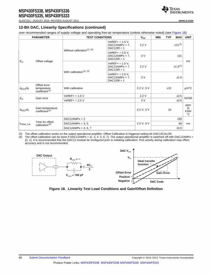
VR+
Gain ErrorOffset Error
DAC Code
DAC VOUT
Ideal transferfunction
R =Load ¥
AVCC
C = 100 pFLoad
2
DAC Output
Positive
Negative
MSP430F5338, MSP430F5336MSP430F5335, MSP430F5333SLAS721C –AUGUST 2010–REVISED AUGUST 2013 www.ti.com
12-Bit DAC, Linearity Specifications (continued)over recommended ranges of supply voltage and operating free-air temperature (unless otherwise noted) (see Figure 18)
PARAMETER TEST CONDITIONS VCC MIN TYP MAX UNITVeREF+ = 1.5 V,DAC12AMPx = 7, 2.2 V ±21 (2)
DAC12IR = 1Without calibration (1) (3)
VeREF+ = 2.5 V,DAC12AMPx = 7, 3 V ±21DAC12IR = 1
EO Offset voltage mVVeREF+ = 1.5 V,DAC12AMPx = 7, 2.2 V ±1.5 (2)
DAC12IR = 1With calibration (1) (3)
VeREF+ = 2.5 V,DAC12AMPx = 7, 3 V ±1.5DAC12IR = 1
Offset errordE(O)/dT temperature With calibration 2.2 V, 3 V ±10 µV/°C
coefficient (1)
VeREF+ = 1.5 V 2.2 V ±2.5EG Gain error %FSR
VeREF+ = 2.5 V 3 V ±2.5ppm
Gain temperature ofdE(G)/dT 2.2 V, 3 V 10coefficient (1) FSR/°C
DAC12AMPx = 2 165Time for offsettOffset_Cal DAC12AMPx = 3, 5 2.2 V, 3 V 66 mscalibration (4)
DAC12AMPx = 4, 6, 7 16.5
(3) The offset calibration works on the output operational amplifier. Offset Calibration is triggered setting bit DAC12CALON(4) The offset calibration can be done if DAC12AMPx = 2, 3, 4, 5, 6, 7. The output operational amplifier is switched off with DAC12AMPx =
0, 1. It is recommended that the DAC12 module be configured prior to initiating calibration. Port activity during calibration may effectaccuracy and is not recommended.
Figure 18. Linearity Test Load Conditions and Gain/Offset Definition
68 Submit Documentation Feedback Copyright © 2010–2013, Texas Instruments Incorporated
Product Folder Links: MSP430F5338 MSP430F5336 MSP430F5335 MSP430F5333

RO/P(DAC12_x)
Max
0.3
AVCC
AV – 0.3 VCC VOUT
Min
RLoad
AVCC
C = 100 pFLoad
2
ILoad
DAC12
O/P(DAC12_x)
MSP430F5338, MSP430F5336MSP430F5335, MSP430F5333
www.ti.com SLAS721C –AUGUST 2010–REVISED AUGUST 2013
12-Bit DAC, Output Specificationsover recommended ranges of supply voltage and operating free-air temperature (unless otherwise noted)
PARAMETER TEST CONDITIONS VCC MIN TYP MAX UNITNo load, VeREF+ = AVCC,DAC12_xDAT = 0h, DAC12IR = 1, 0 0.005DAC12AMPx = 7No load, VeREF+ = AVCC, AVCC –DAC12_xDAT = 0FFFh, DAC12IR = 1, AVCC0.05Output voltage DAC12AMPx = 7
VO range (1) (see 2.2 V, 3 V VRLoad = 3 kΩ, VeREF+ = AVCC,Figure 19)DAC12_xDAT = 0h, DAC12IR = 1, 0 0.1DAC12AMPx = 7RLoad = 3 kΩ, VeREF+ = AVCC, AVCC –DAC12_xDAT = 0FFFh, DAC12IR = 1, AVCC0.13DAC12AMPx = 7
Maximum DAC12CL(DAC12) 2.2 V, 3 V 100 pFload capacitanceDAC12AMPx = 2, DAC12xDAT = 0FFFh, –1VO/P(DAC12) > AVCC – 0.3Maximum DAC12IL(DAC12) 2.2 V, 3 V mAload current DAC12AMPx = 2, DAC12xDAT = 0h, 1VO/P(DAC12) < 0.3 VRLoad = 3 kΩ, VO/P(DAC12) < 0.3 V, 150 250DAC12AMPx = 2, DAC12_xDAT = 0h
Output resistance RLoad = 3 kΩ, VO/P(DAC12) > AVCC – 0.3 V,RO/P(DAC12) 2.2 V, 3 V 150 250 Ω(see Figure 19) DAC12_xDAT = 0FFFhRLoad = 3 kΩ, 60.3 V ≤ VO/P(DAC12) ≤ AVCC – 0.3 V
(1) Data is valid after the offset calibration of the output amplifier.
Figure 19. DAC12_x Output Resistance Tests
Copyright © 2010–2013, Texas Instruments Incorporated Submit Documentation Feedback 69
Product Folder Links: MSP430F5338 MSP430F5336 MSP430F5335 MSP430F5333
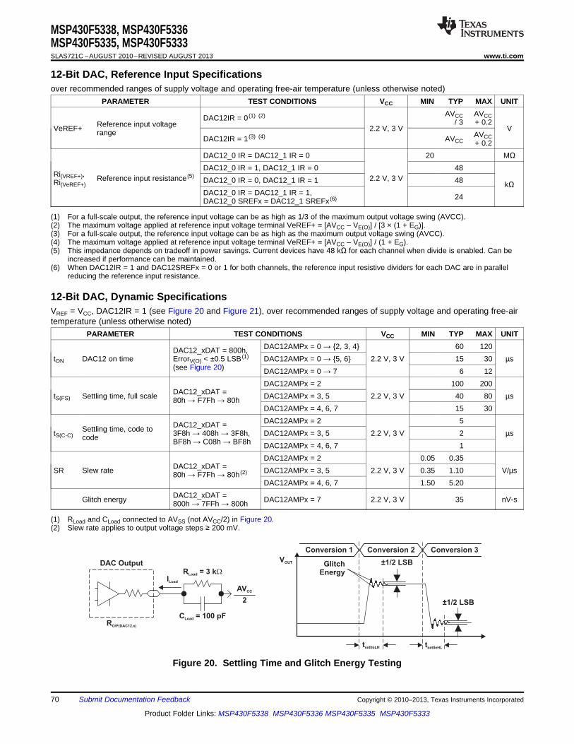
R = 3 kLoad W
AVCC
C = 100 pFLoad
2
DAC Output
RO/P(DAC12.x)
ILoad
Conversion 1 Conversion 2
VOUT
Conversion 3
GlitchEnergy
±1/2 LSB
±1/2 LSB
tsettleLH tsettleHL
MSP430F5338, MSP430F5336MSP430F5335, MSP430F5333SLAS721C –AUGUST 2010–REVISED AUGUST 2013 www.ti.com
12-Bit DAC, Reference Input Specificationsover recommended ranges of supply voltage and operating free-air temperature (unless otherwise noted)
PARAMETER TEST CONDITIONS VCC MIN TYP MAX UNITAVCC AVCCDAC12IR = 0 (1) (2)
/ 3 + 0.2Reference input voltageVeREF+ 2.2 V, 3 V Vrange AVCCDAC12IR = 1 (3) (4) AVCC + 0.2DAC12_0 IR = DAC12_1 IR = 0 20 MΩDAC12_0 IR = 1, DAC12_1 IR = 0 48
Ri(VREF+), Reference input resistance (5) 2.2 V, 3 VDAC12_0 IR = 0, DAC12_1 IR = 1 48Ri(VeREF+) kΩDAC12_0 IR = DAC12_1 IR = 1, 24DAC12_0 SREFx = DAC12_1 SREFx (6)
(1) For a full-scale output, the reference input voltage can be as high as 1/3 of the maximum output voltage swing (AVCC).(2) The maximum voltage applied at reference input voltage terminal VeREF+ = [AVCC – VE(O)] / [3 × (1 + EG)].(3) For a full-scale output, the reference input voltage can be as high as the maximum output voltage swing (AVCC).(4) The maximum voltage applied at reference input voltage terminal VeREF+ = [AVCC – VE(O)] / (1 + EG).(5) This impedance depends on tradeoff in power savings. Current devices have 48 kΩ for each channel when divide is enabled. Can be
increased if performance can be maintained.(6) When DAC12IR = 1 and DAC12SREFx = 0 or 1 for both channels, the reference input resistive dividers for each DAC are in parallel
reducing the reference input resistance.
12-Bit DAC, Dynamic SpecificationsVREF = VCC, DAC12IR = 1 (see Figure 20 and Figure 21), over recommended ranges of supply voltage and operating free-airtemperature (unless otherwise noted)
PARAMETER TEST CONDITIONS VCC MIN TYP MAX UNITDAC12AMPx = 0 → 2, 3, 4 60 120DAC12_xDAT = 800h,
tON DAC12 on time ErrorV(O) < ±0.5 LSB (1) DAC12AMPx = 0 → 5, 6 2.2 V, 3 V 15 30 µs(see Figure 20) DAC12AMPx = 0 → 7 6 12
DAC12AMPx = 2 100 200DAC12_xDAT =tS(FS) Settling time, full scale DAC12AMPx = 3, 5 2.2 V, 3 V 40 80 µs80h → F7Fh → 80h
DAC12AMPx = 4, 6, 7 15 30DAC12AMPx = 2 5DAC12_xDAT =Settling time, code totS(C-C) 3F8h → 408h → 3F8h, DAC12AMPx = 3, 5 2.2 V, 3 V 2 µscode BF8h → C08h → BF8h DAC12AMPx = 4, 6, 7 1DAC12AMPx = 2 0.05 0.35
DAC12_xDAT =SR Slew rate DAC12AMPx = 3, 5 2.2 V, 3 V 0.35 1.10 V/µs80h → F7Fh → 80h (2)
DAC12AMPx = 4, 6, 7 1.50 5.20DAC12_xDAT =Glitch energy DAC12AMPx = 7 2.2 V, 3 V 35 nV-s800h → 7FFh → 800h
(1) RLoad and CLoad connected to AVSS (not AVCC/2) in Figure 20.(2) Slew rate applies to output voltage steps ≥ 200 mV.
Figure 20. Settling Time and Glitch Energy Testing
70 Submit Documentation Feedback Copyright © 2010–2013, Texas Instruments Incorporated
Product Folder Links: MSP430F5338 MSP430F5336 MSP430F5335 MSP430F5333
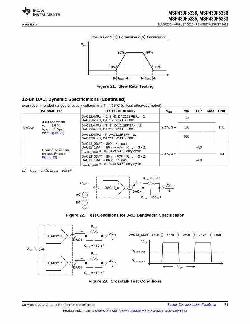
DAC12_xDAT 080h
VOUT
f oggleT
7F7h
VDAC12_yOUT
080h 7F7h 080h
VDAC12_xOUT
RLoad
AVCC
CLoad = 100 pF
2
ILoad
DAC12_1
RLoad
AVCC
C = 100 pFLoad
2
ILoad
DAC12_0DAC0
DAC1
VREF+
VeREF+
AC
DC
R = 3 kLoad W
AVCC
C = 100 pFLoad
2
ILoad
DAC12_xDACx
Conversion 1 Conversion 2
VOUT
Conversion 3
10%
tSRLH
tSRHL
90%
10%
90%
MSP430F5338, MSP430F5336MSP430F5335, MSP430F5333
www.ti.com SLAS721C –AUGUST 2010–REVISED AUGUST 2013
Figure 21. Slew Rate Testing
12-Bit DAC, Dynamic Specifications (Continued)over recommended ranges of supply voltage and TA = 25°C (unless otherwise noted)
PARAMETER TEST CONDITIONS VCC MIN TYP MAX UNITDAC12AMPx = 2, 3, 4, DAC12SREFx = 2, 40DAC12IR = 1, DAC12_xDAT = 800h3-dB bandwidth,
VDC = 1.5 V, DAC12AMPx = 5, 6, DAC12SREFx = 2,BW–3dB 2.2 V, 3 V 180 kHzVAC = 0.1 VPP DAC12IR = 1, DAC12_xDAT = 800h(see Figure 22) DAC12AMPx = 7, DAC12SREFx = 2, 550DAC12IR = 1, DAC12_xDAT = 800h
DAC12_0DAT = 800h, No load,DAC12_1DAT = 80h ↔ F7Fh, RLoad = 3 kΩ, –80
Channel-to-channel fDAC12_0OUT = 10 kHz at 50/50 duty cyclecrosstalk (1) (see 2.2 V, 3 V dB
DAC12_0DAT = 80h ↔ F7Fh, RLoad = 3 kΩ,Figure 23)DAC12_1DAT = 800h, No load, –80fDAC12_0OUT = 10 kHz at 50/50 duty cycle
(1) RLoad = 3 kΩ, CLoad = 100 pF
Figure 22. Test Conditions for 3-dB Bandwidth Specification
Figure 23. Crosstalk Test Conditions
Copyright © 2010–2013, Texas Instruments Incorporated Submit Documentation Feedback 71
Product Folder Links: MSP430F5338 MSP430F5336 MSP430F5335 MSP430F5333
MSP430F5338, MSP430F5336MSP430F5335, MSP430F5333SLAS721C –AUGUST 2010–REVISED AUGUST 2013 www.ti.com
Comparator_Bover recommended ranges of supply voltage and operating free-air temperature (unless otherwise noted)
PARAMETER TEST CONDITIONS VCC MIN TYP MAX UNITVCC Supply voltage 1.8 3.6 V
1.8 V 40Comparator operating supply CBPWRMD = 00 2.2 V 30 50current into AVCC terminal,IAVCC_COMP 3 V 40 65 µAExcludes reference resistor
CBPWRMD = 01 2.2 V, 3 V 10 30ladderCBPWRMD = 10 2.2 V, 3 V 0.1 0.5
Quiescent current of localIAVCC_REF reference voltage amplifier CBREFACC = 1, CBREFLx = 01 22 µA
into AVCC terminalVIC Common mode input range 0 VCC - 1 V
CBPWRMD = 00 ±20VOFFSET Input offset voltage mV
CBPWRMD = 01, 10 ±10CIN Input capacitance 5 pF
ON - switch closed 3 4 kΩRSIN Series input resistance
OFF - switch opened 50 MΩCBPWRMD = 00, CBF = 0 450 ns
Propagation delay, responsetPD CBPWRMD = 01, CBF = 0 600 nstimeCBPWRMD = 10, CBF = 0 50 µsCBPWRMD = 00, CBON = 1, CBF = 1, 0.35 0.6 1.0 µsCBFDLY = 00CBPWRMD = 00, CBON = 1, CBF = 1, 0.6 1.0 1.8 µsCBFDLY = 01Propagation delay with filtertPD,filter active CBPWRMD = 00, CBON = 1, CBF = 1, 1.0 1.8 3.4 µsCBFDLY = 10CBPWRMD = 00, CBON = 1, CBF = 1, 1.8 3.4 6.5 µsCBFDLY = 11
Comparator enable time, CBON = 0 to CBON = 1tEN_CMP 1 2 µssettling time CBPWRMD = 00, 01, 10Resistor reference enabletEN_REF CBON = 0 to CBON = 1 0.3 1.5 µstime
VIN × VIN × VIN ×Reference voltage for a given VIN = reference into resistor ladder,VCB_REF (n+0.5) (n+1) (n+1.5) Vtap n = 0 to 31 / 32 / 32 / 32
72 Submit Documentation Feedback Copyright © 2010–2013, Texas Instruments Incorporated
Product Folder Links: MSP430F5338 MSP430F5336 MSP430F5335 MSP430F5333
MSP430F5338, MSP430F5336MSP430F5335, MSP430F5333
www.ti.com SLAS721C –AUGUST 2010–REVISED AUGUST 2013
Ports PU.0 and PU.1over recommended ranges of supply voltage and operating free-air temperature (unless otherwise noted)
PARAMETER TEST CONDITIONS VCC MIN TYP MAX UNITVLDOO = 3.3 V ± 10%, IOH = -25 mA,VOH High-level output voltage 2.4 VSee Figure 25 for typical characteristicsVLDOO = 3.3 V ± 10%, IOL = 25 mA,VOL Low-level output voltage 0.4 VSee Figure 24 for typical characteristicsVLDOO = 3.3 V ± 10%,VIH High-level input voltage 2.0 VSee Figure 26 for typical characteristicsVLDOO = 3.3 V ± 10%,VIL Low-level input voltage 0.8 VSee Figure 26 for typical characteristics
Copyright © 2010–2013, Texas Instruments Incorporated Submit Documentation Feedback 73
Product Folder Links: MSP430F5338 MSP430F5336 MSP430F5335 MSP430F5333

TYPICAL PU.0, PU.1 INPUT THRESHOLD
0.0
0.2
0.4
0.6
0.8
1.0
1.2
1.4
1.6
1.8
2.0
1.8 2.2 2.6 3 3.4
LDOO Supply Voltage, VLDOO - V
Inp
ut
Th
resh
old
-V
VIT+, postive-going input threshold
VIT- , negative-going input threshold
TA = 25 °C, 85 °C
TYPICAL HIGH-LEVEL OUTPUT CURRENT
vs
HIGH-LEVEL OUTPUT VOLTAGE
-90
-80
-70
-60
-50
-40
-30
-20
-10
0
0.5 1 1.5 2 2.5 3
VOH - High-Level Output Voltage - V
I OH
- Ty
pic
al
Hig
h-L
ev
el
Ou
tpu
t C
urr
en
t -
mA
V = 1.8 V
T = 85 ºC
CC
A
V = 1.8 V
T = 25 ºC
CC
A
V = 3.0 V
T = 85 ºC
CC
A
V = 3.0 V
T = 25 ºC
CC
A
TYPICAL LOW-LEVEL OUTPUT CURRENT
vs
LOW-LEVEL OUTPUT VOLTAGE
0
10
20
30
40
50
60
70
80
90
0 0.1 0.2 0.3 0.4 0.5 0.6 0.7 0.8 0.9 1 1.1 1.2
VOL - Low-Level Output Voltage - V
I OL
- Typ
ical L
ow
-Level O
utp
ut
Cu
rren
t -
mA
V = 3.0 V
T = 85 ºC
CC
A
V = 1.8 V
T = 85 ºC
CC
A
V = 1.8 V
T = 25 ºC
CC
A
V = 3.0 V
T = 25 ºC
CC
A
MSP430F5338, MSP430F5336MSP430F5335, MSP430F5333SLAS721C –AUGUST 2010–REVISED AUGUST 2013 www.ti.com
Figure 24. Ports PU.0, PU.1 Typical Low-Level Output Characteristics
Figure 25. Ports PU.0, PU.1 Typical High-Level Output Characteristics
Figure 26. Ports PU.0, PU.1 Typical Input Threshold Characteristics
74 Submit Documentation Feedback Copyright © 2010–2013, Texas Instruments Incorporated
Product Folder Links: MSP430F5338 MSP430F5336 MSP430F5335 MSP430F5333

MSP430F5338, MSP430F5336MSP430F5335, MSP430F5333
www.ti.com SLAS721C –AUGUST 2010–REVISED AUGUST 2013
LDO-PWR (LDO Power System)over recommended ranges of supply voltage and operating free-air temperature (unless otherwise noted)
PARAMETER TEST CONDITIONS VCC MIN TYP MAX UNITVLAUNCH LDO input detection threshold 3.75 VVLDOI LDO input voltage Normal operation 3.76 5.5 VVLDO LDO output voltage 3.3 ±9% V
LDOO terminal input voltage with LDOVLDO_EXT LDO disabled 1.8 3.6 VdisabledILDOO Maximum external current from LDOO terminal LDO is on 20 mAIDET LDO current overload detection (1) 60 100 mACLDOI LDOI terminal recommended capacitance 4.7 µFCLDOO LDOO terminal recommended capacitance 220 nF
Within 2%,tENABLE Settling time VLDO 2 msrecommended capacitances
(1) A current overload is detected when the total current supplied from the LDO exceeds this value.
Flash Memoryover recommended ranges of supply voltage and operating free-air temperature (unless otherwise noted)
TESTPARAMETER MIN TYP MAX UNITCONDITIONSDVCC(PGM/ERASE) Program and erase supply voltage 1.8 3.6 VIPGM Average supply current from DVCC during program 3 5 mAIERASE Average supply current from DVCC during erase 6 11 mA
Average supply current from DVCC during mass erase or bankIMERASE, IBANK 6 11 mAerasetCPT Cumulative program time See (1) 16 ms
Program and erase endurance 104 105 cyclestRetention Data retention duration TJ = 25°C 100 yearstWord Word or byte program time See (2) 64 85 µstBlock, 0 Block program time for first byte or word See (2) 49 65 µs
Block program time for each additional byte or word, except for lasttBlock, 1–(N–1) See (2) 37 49 µsbyte or wordtBlock, N Block program time for last byte or word See (2) 55 73 µs
Erase time for segment, mass erase, and bank erase whentSeg Erase See (2) 23 32 msavailableMCLK frequency in marginal read modefMCLK,MGR 0 1 MHz(FCTL4.MGR0 = 1 or FCTL4.MGR1 = 1)
(1) The cumulative program time must not be exceeded when writing to a 128-byte flash block. This parameter applies to all programmingmethods: individual word or byte write and block write modes.
(2) These values are hardwired into the flash controller's state machine.
JTAG and Spy-Bi-Wire Interfaceover recommended ranges of supply voltage and operating free-air temperature (unless otherwise noted)
TESTPARAMETER MIN TYP MAX UNITCONDITIONSfSBW Spy-Bi-Wire input frequency 2.2 V, 3 V 0 20 MHztSBW,Low Spy-Bi-Wire low clock pulse duration 2.2 V, 3 V 0.025 15 µs
Spy-Bi-Wire enable time (TEST high to acceptance of first clocktSBW, En 2.2 V, 3 V 1 µsedge) (1)
tSBW,Rst Spy-Bi-Wire return to normal operation time 15 100 µs
(1) Tools that access the Spy-Bi-Wire interface must wait for the tSBW,En time after pulling the TEST/SBWTCK pin high before applying thefirst SBWTCK clock edge.
Copyright © 2010–2013, Texas Instruments Incorporated Submit Documentation Feedback 75
Product Folder Links: MSP430F5338 MSP430F5336 MSP430F5335 MSP430F5333
MSP430F5338, MSP430F5336MSP430F5335, MSP430F5333SLAS721C –AUGUST 2010–REVISED AUGUST 2013 www.ti.com
JTAG and Spy-Bi-Wire Interface (continued)over recommended ranges of supply voltage and operating free-air temperature (unless otherwise noted)
TESTPARAMETER MIN TYP MAX UNITCONDITIONS2.2 V 0 5 MHz
fTCK TCK input frequency (4-wire JTAG) (2)3 V 0 10 MHz
Rinternal Internal pulldown resistance on TEST 2.2 V, 3 V 45 60 80 kΩ
(2) fTCK may be restricted to meet the timing requirements of the module selected.
76 Submit Documentation Feedback Copyright © 2010–2013, Texas Instruments Incorporated
Product Folder Links: MSP430F5338 MSP430F5336 MSP430F5335 MSP430F5333
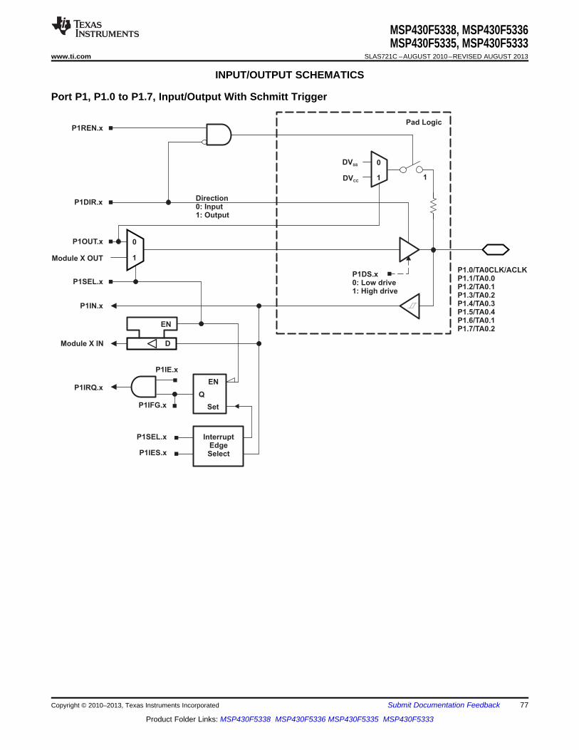
P1.0/TA0CLK/ACLKP1.1/TA0.0P1.2/TA0.1P1.3/TA0.2P1.4/TA0.3P1.5/TA0.4P1.6/TA0.1P1.7/TA0.2
Direction0: Input1: Output
P1SEL.x
P1DIR.x
P1IN.x
P1IRQ.x
EN
Module X IN
1
0
Module X OUT
P1OUT.x
InterruptEdgeSelect
Q
EN
Set
P1SEL.x
P1IES.x
P1IFG.x
P1IE.x
1
0DVSS
DVCC
P1REN.xPad Logic
1
P1DS.x0: Low drive1: High drive
D
MSP430F5338, MSP430F5336MSP430F5335, MSP430F5333
www.ti.com SLAS721C –AUGUST 2010–REVISED AUGUST 2013
INPUT/OUTPUT SCHEMATICS
Port P1, P1.0 to P1.7, Input/Output With Schmitt Trigger
Copyright © 2010–2013, Texas Instruments Incorporated Submit Documentation Feedback 77
Product Folder Links: MSP430F5338 MSP430F5336 MSP430F5335 MSP430F5333
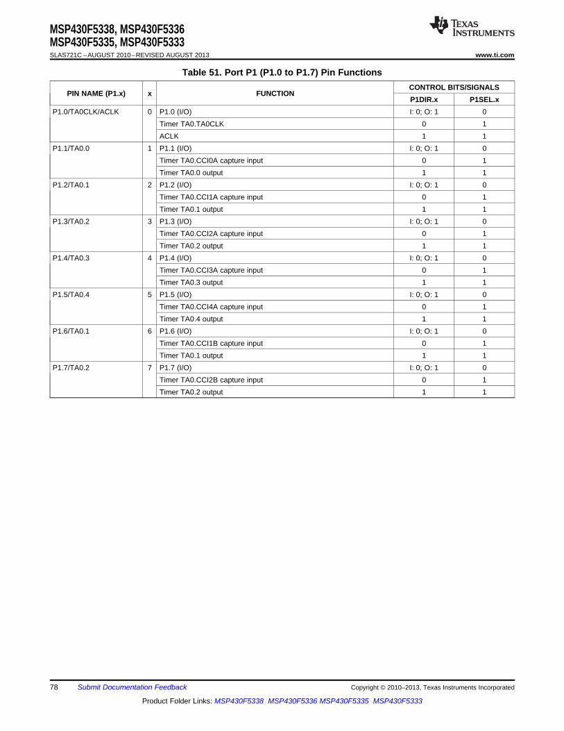
MSP430F5338, MSP430F5336MSP430F5335, MSP430F5333SLAS721C –AUGUST 2010–REVISED AUGUST 2013 www.ti.com
Table 51. Port P1 (P1.0 to P1.7) Pin FunctionsCONTROL BITS/SIGNALS
PIN NAME (P1.x) x FUNCTIONP1DIR.x P1SEL.x
P1.0/TA0CLK/ACLK 0 P1.0 (I/O) I: 0; O: 1 0Timer TA0.TA0CLK 0 1ACLK 1 1
P1.1/TA0.0 1 P1.1 (I/O) I: 0; O: 1 0Timer TA0.CCI0A capture input 0 1Timer TA0.0 output 1 1
P1.2/TA0.1 2 P1.2 (I/O) I: 0; O: 1 0Timer TA0.CCI1A capture input 0 1Timer TA0.1 output 1 1
P1.3/TA0.2 3 P1.3 (I/O) I: 0; O: 1 0Timer TA0.CCI2A capture input 0 1Timer TA0.2 output 1 1
P1.4/TA0.3 4 P1.4 (I/O) I: 0; O: 1 0Timer TA0.CCI3A capture input 0 1Timer TA0.3 output 1 1
P1.5/TA0.4 5 P1.5 (I/O) I: 0; O: 1 0Timer TA0.CCI4A capture input 0 1Timer TA0.4 output 1 1
P1.6/TA0.1 6 P1.6 (I/O) I: 0; O: 1 0Timer TA0.CCI1B capture input 0 1Timer TA0.1 output 1 1
P1.7/TA0.2 7 P1.7 (I/O) I: 0; O: 1 0Timer TA0.CCI2B capture input 0 1Timer TA0.2 output 1 1
78 Submit Documentation Feedback Copyright © 2010–2013, Texas Instruments Incorporated
Product Folder Links: MSP430F5338 MSP430F5336 MSP430F5335 MSP430F5333

P2.0/P2MAP0P2.1/P2MAP1P2.2/P2MAP2P2.3/P2MAP3P2.4/P2MAP4P2.5/P2MAP5P2.6/P2MAP6P2.7/P2MAP7
Direction0: Input1: Output
P2SEL.x
1
0P2DIR.x
P2IN.x
P2IRQ.x
EN
To Port Mapping
1
0
From Port Mapping
P2OUT.x
InterruptEdgeSelect
Q
EN
Set
P2SEL.x
P2IES.x
P2IFG.x
P2IE.x
1
0DVSS
DVCC
P2REN.xPad Logic
1
P2DS.x0: Low drive1: High drive
D
From Port Mapping
MSP430F5338, MSP430F5336MSP430F5335, MSP430F5333
www.ti.com SLAS721C –AUGUST 2010–REVISED AUGUST 2013
Port P2, P2.0 to P2.7, Input/Output With Schmitt Trigger
Copyright © 2010–2013, Texas Instruments Incorporated Submit Documentation Feedback 79
Product Folder Links: MSP430F5338 MSP430F5336 MSP430F5335 MSP430F5333
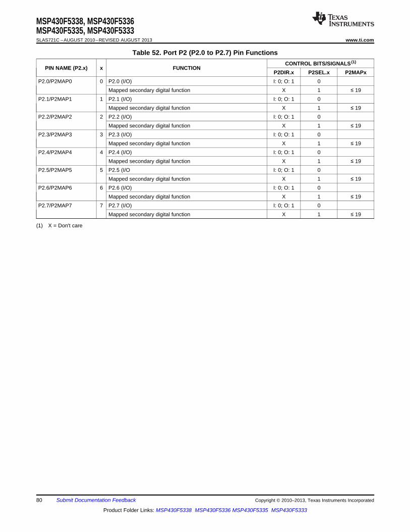
MSP430F5338, MSP430F5336MSP430F5335, MSP430F5333SLAS721C –AUGUST 2010–REVISED AUGUST 2013 www.ti.com
Table 52. Port P2 (P2.0 to P2.7) Pin FunctionsCONTROL BITS/SIGNALS (1)
PIN NAME (P2.x) x FUNCTIONP2DIR.x P2SEL.x P2MAPx
P2.0/P2MAP0 0 P2.0 (I/O) I: 0; O: 1 0Mapped secondary digital function X 1 ≤ 19
P2.1/P2MAP1 1 P2.1 (I/O) I: 0; O: 1 0Mapped secondary digital function X 1 ≤ 19
P2.2/P2MAP2 2 P2.2 (I/O) I: 0; O: 1 0Mapped secondary digital function X 1 ≤ 19
P2.3/P2MAP3 3 P2.3 (I/O) I: 0; O: 1 0Mapped secondary digital function X 1 ≤ 19
P2.4/P2MAP4 4 P2.4 (I/O) I: 0; O: 1 0Mapped secondary digital function X 1 ≤ 19
P2.5/P2MAP5 5 P2.5 (I/O I: 0; O: 1 0Mapped secondary digital function X 1 ≤ 19
P2.6/P2MAP6 6 P2.6 (I/O) I: 0; O: 1 0Mapped secondary digital function X 1 ≤ 19
P2.7/P2MAP7 7 P2.7 (I/O) I: 0; O: 1 0Mapped secondary digital function X 1 ≤ 19
(1) X = Don't care
80 Submit Documentation Feedback Copyright © 2010–2013, Texas Instruments Incorporated
Product Folder Links: MSP430F5338 MSP430F5336 MSP430F5335 MSP430F5333

P3.0/TA1CLK/CBOUTP3.1/TA1.0P3.2/TA1.1P3.3/TA1.2P3.4/TA2CLK/SMCLKP3.5/TA2.0P3.6/TA2.1P3.7/TA2.2
Direction0: Input1: Output
P3SEL.x
P3DIR.x
P3IN.x
EN
Module X IN
1
0
Module X OUT
P3OUT.x
1
0DVSS
DVCC
P3REN.xPad Logic
1
P3DS.x0: Low drive1: High drive
D
P3IRQ.x
InterruptEdgeSelect
Q
EN
Set
P3SEL.x
P3IES.x
P3IFG.x
P3IE.x
MSP430F5338, MSP430F5336MSP430F5335, MSP430F5333
www.ti.com SLAS721C –AUGUST 2010–REVISED AUGUST 2013
Port P3, P3.0 to P3.7, Input/Output With Schmitt Trigger
Copyright © 2010–2013, Texas Instruments Incorporated Submit Documentation Feedback 81
Product Folder Links: MSP430F5338 MSP430F5336 MSP430F5335 MSP430F5333

MSP430F5338, MSP430F5336MSP430F5335, MSP430F5333SLAS721C –AUGUST 2010–REVISED AUGUST 2013 www.ti.com
Table 53. Port P3 (P3.0 to P3.7) Pin FunctionsCONTROL BITS/SIGNALS
PIN NAME (P3.x) x FUNCTIONP3DIR.x P3SEL.x
P3.0/TA1CLK/CBOUT 0 P3.0 (I/O) I: 0; O: 1 0Timer TA1.TA1CLK 0 1CBOUT 1 1
P3.1/TA1.0 1 P3.1 (I/O) I: 0; O: 1 0Timer TA1.CCI0A capture input 0 1Timer TA1.0 output 1 1
P3.2/TA1.1 2 P3.2 (I/O) I: 0; O: 1 0Timer TA1.CCI1A capture input 0 1Timer TA1.1 output 1 1
P3.3/TA1.2 3 P3.3 (I/O) I: 0; O: 1 0Timer TA1.CCI2A capture input 0 1Timer TA1.2 output 1 1
P3.4/TA2CLK/SMCLK 4 P3.4 (I/O) I: 0; O: 1 0Timer TA2.TA2CLK 0 1SMCLK 1 1
P3.5/TA2.0 5 P3.5 (I/O) I: 0; O: 1 0Timer TA2.CCI0A capture input 0 1Timer TA2.0 output 1 1
P3.6/TA2.1 6 P3.6 (I/O) I: 0; O: 1 0Timer TA2.CCI1A capture input 0 1Timer TA2.1 output 1 1
P3.7/TA2.2 7 P3.7 (I/O) I: 0; O: 1 0Timer TA2.CCI2A capture input 0 1Timer TA2.2 output 1 1
82 Submit Documentation Feedback Copyright © 2010–2013, Texas Instruments Incorporated
Product Folder Links: MSP430F5338 MSP430F5336 MSP430F5335 MSP430F5333
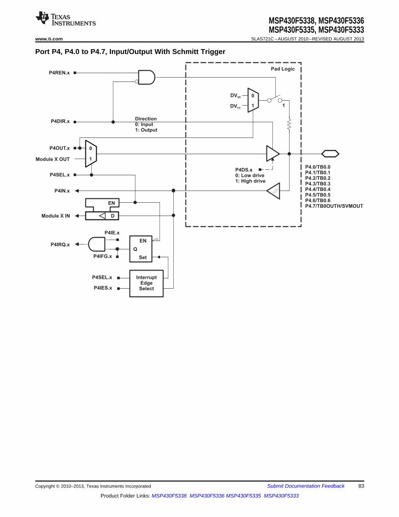
P4.0/TB0.0P4.1/TB0.1P4.2/TB0.2P4.3/TB0.3P4.4/TB0.4P4.5/TB0.5P4.6/TB0.6P4.7/TB0OUTH/SVMOUT
Direction0: Input1: Output
P4SEL.x
P4DIR.x
P4IN.x
EN
Module X IN
1
0
Module X OUT
P4OUT.x
1
0DVSS
DVCC
P4REN.xPad Logic
1
P4DS.x0: Low drive1: High drive
D
P4IRQ.x
InterruptEdgeSelect
Q
EN
Set
P4SEL.x
P4IES.x
P4IFG.x
P4IE.x
MSP430F5338, MSP430F5336MSP430F5335, MSP430F5333
www.ti.com SLAS721C –AUGUST 2010–REVISED AUGUST 2013
Port P4, P4.0 to P4.7, Input/Output With Schmitt Trigger
Copyright © 2010–2013, Texas Instruments Incorporated Submit Documentation Feedback 83
Product Folder Links: MSP430F5338 MSP430F5336 MSP430F5335 MSP430F5333
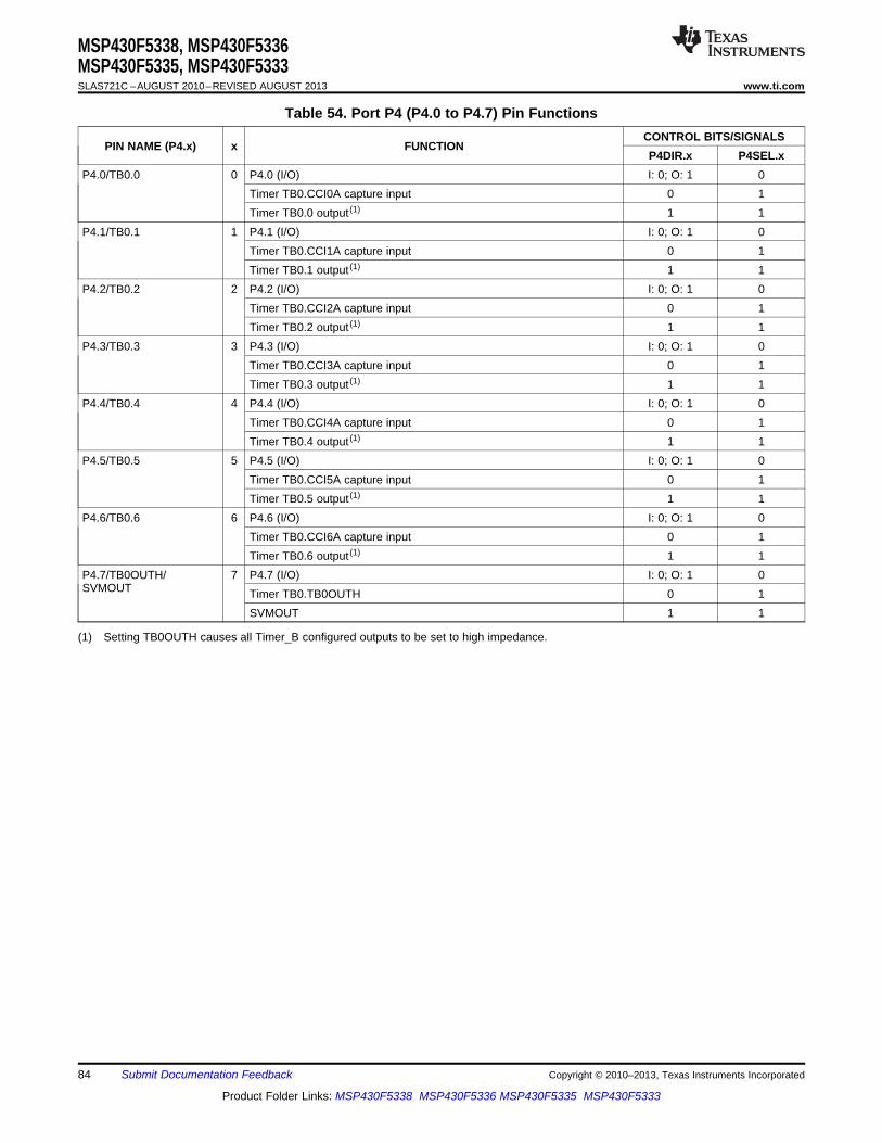
MSP430F5338, MSP430F5336MSP430F5335, MSP430F5333SLAS721C –AUGUST 2010–REVISED AUGUST 2013 www.ti.com
Table 54. Port P4 (P4.0 to P4.7) Pin FunctionsCONTROL BITS/SIGNALS
PIN NAME (P4.x) x FUNCTIONP4DIR.x P4SEL.x
P4.0/TB0.0 0 P4.0 (I/O) I: 0; O: 1 0Timer TB0.CCI0A capture input 0 1Timer TB0.0 output (1) 1 1
P4.1/TB0.1 1 P4.1 (I/O) I: 0; O: 1 0Timer TB0.CCI1A capture input 0 1Timer TB0.1 output (1) 1 1
P4.2/TB0.2 2 P4.2 (I/O) I: 0; O: 1 0Timer TB0.CCI2A capture input 0 1Timer TB0.2 output (1) 1 1
P4.3/TB0.3 3 P4.3 (I/O) I: 0; O: 1 0Timer TB0.CCI3A capture input 0 1Timer TB0.3 output (1) 1 1
P4.4/TB0.4 4 P4.4 (I/O) I: 0; O: 1 0Timer TB0.CCI4A capture input 0 1Timer TB0.4 output (1) 1 1
P4.5/TB0.5 5 P4.5 (I/O) I: 0; O: 1 0Timer TB0.CCI5A capture input 0 1Timer TB0.5 output (1) 1 1
P4.6/TB0.6 6 P4.6 (I/O) I: 0; O: 1 0Timer TB0.CCI6A capture input 0 1Timer TB0.6 output (1) 1 1
P4.7/TB0OUTH/ 7 P4.7 (I/O) I: 0; O: 1 0SVMOUT Timer TB0.TB0OUTH 0 1
SVMOUT 1 1
(1) Setting TB0OUTH causes all Timer_B configured outputs to be set to high impedance.
84 Submit Documentation Feedback Copyright © 2010–2013, Texas Instruments Incorporated
Product Folder Links: MSP430F5338 MSP430F5336 MSP430F5335 MSP430F5333
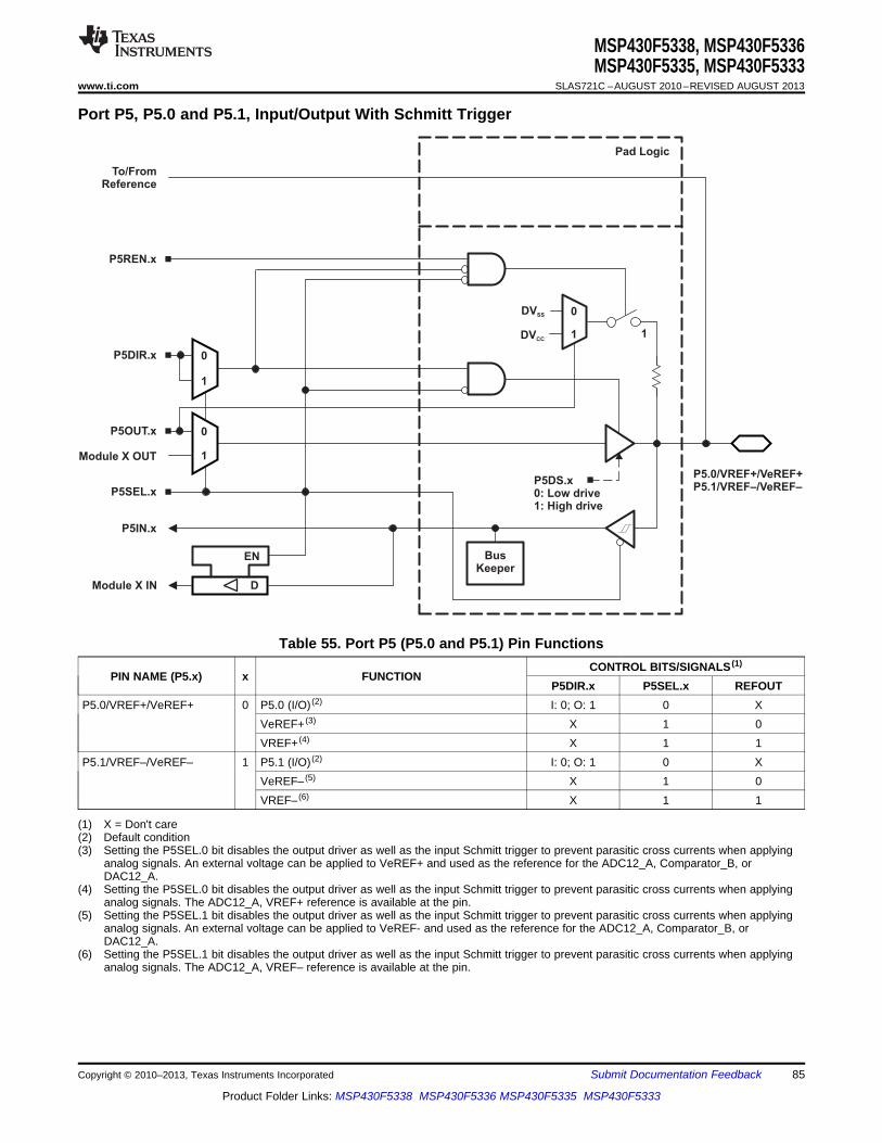
P5.0/VREF+/VeREF+P5.1/VREF–/VeREF–P5SEL.x
1
0P5DIR.x
P5IN.x
EN
Module X IN
1
0
Module X OUT
P5OUT.x
1
0DVSS
DVCC
P5REN.x
Pad Logic
1
P5DS.x0: Low drive1: High drive
D
BusKeeper
To/FromReference
MSP430F5338, MSP430F5336MSP430F5335, MSP430F5333
www.ti.com SLAS721C –AUGUST 2010–REVISED AUGUST 2013
Port P5, P5.0 and P5.1, Input/Output With Schmitt Trigger
Table 55. Port P5 (P5.0 and P5.1) Pin FunctionsCONTROL BITS/SIGNALS (1)
PIN NAME (P5.x) x FUNCTIONP5DIR.x P5SEL.x REFOUT
P5.0/VREF+/VeREF+ 0 P5.0 (I/O) (2) I: 0; O: 1 0 XVeREF+ (3) X 1 0VREF+ (4) X 1 1
P5.1/VREF–/VeREF– 1 P5.1 (I/O) (2) I: 0; O: 1 0 XVeREF– (5) X 1 0VREF– (6) X 1 1
(1) X = Don't care(2) Default condition(3) Setting the P5SEL.0 bit disables the output driver as well as the input Schmitt trigger to prevent parasitic cross currents when applying
analog signals. An external voltage can be applied to VeREF+ and used as the reference for the ADC12_A, Comparator_B, orDAC12_A.
(4) Setting the P5SEL.0 bit disables the output driver as well as the input Schmitt trigger to prevent parasitic cross currents when applyinganalog signals. The ADC12_A, VREF+ reference is available at the pin.
(5) Setting the P5SEL.1 bit disables the output driver as well as the input Schmitt trigger to prevent parasitic cross currents when applyinganalog signals. An external voltage can be applied to VeREF- and used as the reference for the ADC12_A, Comparator_B, orDAC12_A.
(6) Setting the P5SEL.1 bit disables the output driver as well as the input Schmitt trigger to prevent parasitic cross currents when applyinganalog signals. The ADC12_A, VREF– reference is available at the pin.
Copyright © 2010–2013, Texas Instruments Incorporated Submit Documentation Feedback 85
Product Folder Links: MSP430F5338 MSP430F5336 MSP430F5335 MSP430F5333
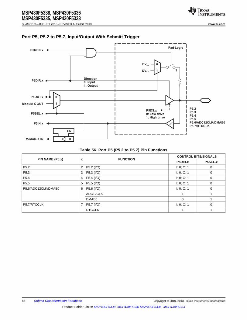
P5.2P5.3P5.4P5.5P5.6/ADC12CLK/DMAE0P5.7/RTCCLK
Direction0: Input1: Output
P5SEL.x
P5DIR.x
P5IN.x
EN
Module X IN
1
0
Module X OUT
P5OUT.x
1
0DVSS
DVCC
P5REN.xPad Logic
1
P5DS.x0: Low drive1: High drive
D
MSP430F5338, MSP430F5336MSP430F5335, MSP430F5333SLAS721C –AUGUST 2010–REVISED AUGUST 2013 www.ti.com
Port P5, P5.2 to P5.7, Input/Output With Schmitt Trigger
Table 56. Port P5 (P5.2 to P5.7) Pin FunctionsCONTROL BITS/SIGNALS
PIN NAME (P5.x) x FUNCTIONP5DIR.x P5SEL.x
P5.2 2 P5.2 (I/O) I: 0; O: 1 0P5.3 3 P5.3 (I/O) I: 0; O: 1 0P5.4 4 P5.4 (I/O) I: 0; O: 1 0P5.5 5 P5.5 (I/O) I: 0; O: 1 0P5.6/ADC12CLK/DMAE0 6 P5.6 (I/O) I: 0; O: 1 0
ADC12CLK 1 1DMAE0 0 1
P5.7/RTCCLK 7 P5.7 (I/O) I: 0; O: 1 0RTCCLK 1 1
86 Submit Documentation Feedback Copyright © 2010–2013, Texas Instruments Incorporated
Product Folder Links: MSP430F5338 MSP430F5336 MSP430F5335 MSP430F5333
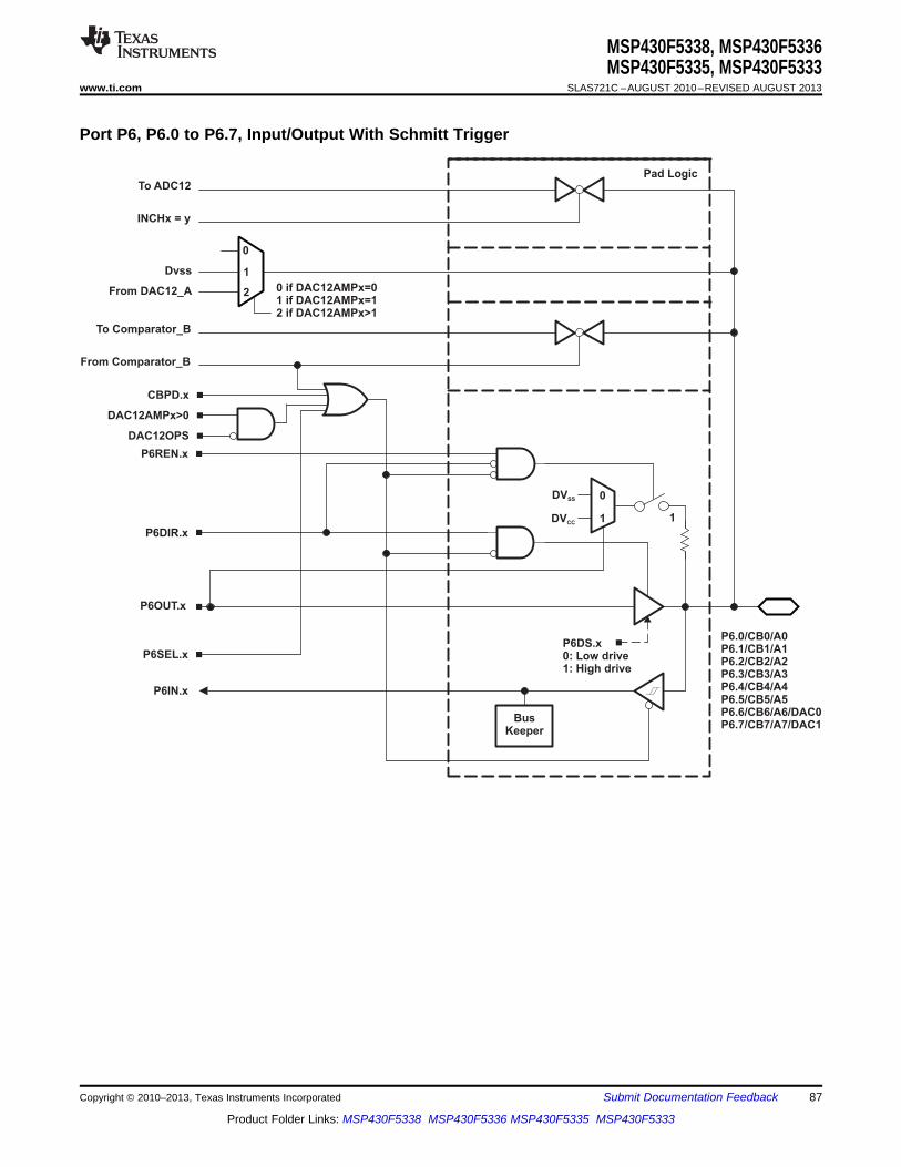
P6SEL.x
P6DIR.x
P6IN.x
P6OUT.x
1
0DVSS
DVCC
P6REN.x
Pad Logic
1
P6DS.x0: Low drive1: High drive
BusKeeper
To ADC12
P6.0/CB0/A0P6.1/CB1/A1P6.2/CB2/A2P6.3/CB3/A3P6.4/CB4/A4P6.5/CB5/A5P6.6/CB6/A6/DAC0P6.7/CB7/A7/DAC1
INCHx = y
From DAC12_A
To Comparator_B
From Comparator_B
CBPD.x
0
1
2
Dvss
0 if DAC12AMPx=01 if DAC12AMPx=12 if DAC12AMPx>1
DAC12AMPx>0
DAC12OPS
MSP430F5338, MSP430F5336MSP430F5335, MSP430F5333
www.ti.com SLAS721C –AUGUST 2010–REVISED AUGUST 2013
Port P6, P6.0 to P6.7, Input/Output With Schmitt Trigger
Copyright © 2010–2013, Texas Instruments Incorporated Submit Documentation Feedback 87
Product Folder Links: MSP430F5338 MSP430F5336 MSP430F5335 MSP430F5333

MSP430F5338, MSP430F5336MSP430F5335, MSP430F5333SLAS721C –AUGUST 2010–REVISED AUGUST 2013 www.ti.com
Table 57. Port P6 (P6.0 to P6.7) Pin FunctionsCONTROL BITS/SIGNALS (1)
PIN NAME (P6.x) x FUNCTIONP6DIR.x P6SEL.x CBPD.x DAC12OPS DAC12AMPx
P6.0/CB0/A0 0 P6.0 (I/O) I: 0; O: 1 0 0 n/a n/aCB0 X X 1 n/a n/aA0 (2) (3) X 1 X n/a n/a
P6.1/CB1/A1 1 P6.1 (I/O) I: 0; O: 1 0 0 n/a n/aCB1 X X 1 n/a n/aA1 (2) (3) X 1 X n/a n/a
P6.2/CB2/A2 2 P6.2 (I/O) I: 0; O: 1 0 0 n/a n/aCB2 X X 1 n/a n/aA2 (2) (3) X 1 X n/a n/a
P6.3/CB3/A3 3 P6.3 (I/O) I: 0; O: 1 0 0 n/a n/aCB3 X X 1 n/a n/aA3 (2) (3) X 1 X n/a n/a
P6.4/CB4/A4 4 P6.4 (I/O) I: 0; O: 1 0 0 n/a n/aCB4 X X 1 n/a n/aA4 (2) (3) X 1 X n/a n/a
P6.5/CB5/A5 5 P6.5 (I/O) I: 0; O: 1 0 0 n/a n/aCB5 X X 1 n/a n/aA5 (4) (2) (3) X 1 X n/a n/a
P6.6/CB6/A6/DAC0 6 P6.6 (I/O) I: 0; O: 1 0 0 X 0CB6 X X 1 X 0A6 (2) (3) X 1 X X 0DAC0 X X X 0 >1
P6.7/CB7/A7/DAC1 7 P6.7 (I/O) I: 0; O: 1 0 0 X 0CB7 X X 1 X 0A7 (2) (3) X 1 X X 0DAC1 X X X 0 >1
(1) X = Don't care(2) Setting the P6SEL.x bit disables the output driver as well as the input Schmitt trigger to prevent parasitic cross currents when applying
analog signals.(3) The ADC12_A channel Ax is connected internally to AVSS if not selected via the respective INCHx bits.(4) X = Don't care
88 Submit Documentation Feedback Copyright © 2010–2013, Texas Instruments Incorporated
Product Folder Links: MSP430F5338 MSP430F5336 MSP430F5335 MSP430F5333

P7.2/XT2IN
P7SEL.2
1
0P7DIR.2
P7IN.2
P7OUT.2
1
0DVSS
DVCC
P7REN.2
Pad Logic
1
P7DS.20: Low drive1: High drive
BusKeeper
To XT2
MSP430F5338, MSP430F5336MSP430F5335, MSP430F5333
www.ti.com SLAS721C –AUGUST 2010–REVISED AUGUST 2013
Port P7, P7.2, Input/Output With Schmitt Trigger
Copyright © 2010–2013, Texas Instruments Incorporated Submit Documentation Feedback 89
Product Folder Links: MSP430F5338 MSP430F5336 MSP430F5335 MSP430F5333
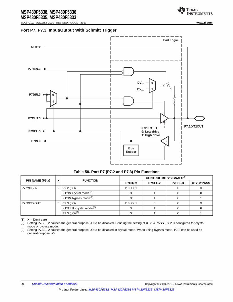
P7.3/XT2OUT
P7SEL.3
1
0P7DIR.3
P7IN.3
P7OUT.3
1
0DVSS
DVCC
P7REN.3
Pad Logic
1
P7DS.30: Low drive1: High drive
BusKeeper
To XT2
MSP430F5338, MSP430F5336MSP430F5335, MSP430F5333SLAS721C –AUGUST 2010–REVISED AUGUST 2013 www.ti.com
Port P7, P7.3, Input/Output With Schmitt Trigger
Table 58. Port P7 (P7.2 and P7.3) Pin FunctionsCONTROL BITS/SIGNALS (1)
PIN NAME (P5.x) x FUNCTIONP7DIR.x P7SEL.2 P7SEL.3 XT2BYPASS
P7.2/XT2IN 2 P7.2 (I/O) I: 0; O: 1 0 X XXT2IN crystal mode (2) X 1 X 0XT2IN bypass mode (2) X 1 X 1
P7.3/XT2OUT 3 P7.3 (I/O) I: 0; O: 1 0 X XXT2OUT crystal mode (3) X 1 X 0P7.3 (I/O) (3) X 1 X 1
(1) X = Don't care(2) Setting P7SEL.2 causes the general-purpose I/O to be disabled. Pending the setting of XT2BYPASS, P7.2 is configured for crystal
mode or bypass mode.(3) Setting P7SEL.2 causes the general-purpose I/O to be disabled in crystal mode. When using bypass mode, P7.3 can be used as
general-purpose I/O.
90 Submit Documentation Feedback Copyright © 2010–2013, Texas Instruments Incorporated
Product Folder Links: MSP430F5338 MSP430F5336 MSP430F5335 MSP430F5333
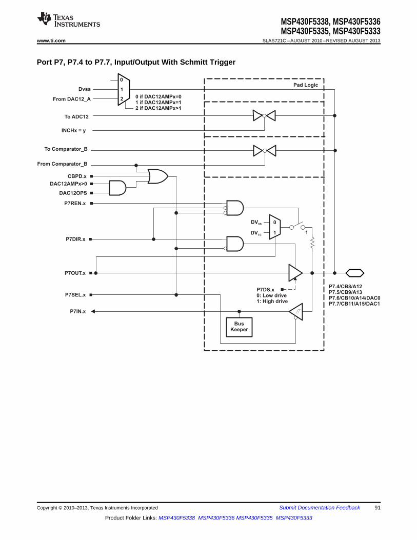
P7SEL.x
P7DIR.x
P7IN.x
P7OUT.x
1
0DVSS
DVCC
P7REN.x
Pad Logic
1
P7DS.x0: Low drive1: High drive
BusKeeper
From DAC12_A
P7.4/CB8/A12P7.5/CB9/A13P7.6/CB10/A14/DAC0P7.7/CB11/A15/DAC1
INCHx = y
To ADC12
To Comparator_B
From Comparator_B
CBPD.x
0
1
2
Dvss
0 if DAC12AMPx=01 if DAC12AMPx=12 if DAC12AMPx>1
DAC12AMPx>0
DAC12OPS
MSP430F5338, MSP430F5336MSP430F5335, MSP430F5333
www.ti.com SLAS721C –AUGUST 2010–REVISED AUGUST 2013
Port P7, P7.4 to P7.7, Input/Output With Schmitt Trigger
Copyright © 2010–2013, Texas Instruments Incorporated Submit Documentation Feedback 91
Product Folder Links: MSP430F5338 MSP430F5336 MSP430F5335 MSP430F5333
MSP430F5338, MSP430F5336MSP430F5335, MSP430F5333SLAS721C –AUGUST 2010–REVISED AUGUST 2013 www.ti.com
Table 59. Port P7 (P7.4 to P7.7) Pin FunctionsCONTROL BITS/SIGNALS (1)
PIN NAME (P7.x) x FUNCTIONP7DIR.x P7SEL.x CBPD.x DAC12OPS DAC12AMPx
P7.4/CB8/A12 4 P7.4 (I/O) I: 0; O: 1 0 0 n/a n/aComparator_B input CB8 X X 1 n/a n/aA12 (2) (3) X 1 X n/a n/a
P7.5/CB9/A13 5 P7.5 (I/O) I: 0; O: 1 0 0 n/a n/aComparator_B input CB9 X X 1 n/a n/aA13 (2) (3) X 1 X n/a n/a
P7.6/CB10/A14/DAC0 6 P7.6 (I/O) I: 0; O: 1 0 0 X 0Comparator_B input CB10 X X 1 X 0A14 (2) (3) X 1 X X 0DAC12_A output DAC0 X X X 1 >1
P7.7/CB11/A15/DAC1 7 P7.7 (I/O) I: 0; O: 1 0 0 X 0Comparator_B input CB11 X X 1 X 0A15 (2) (3) X 1 X X 0DAC12_A output DAC1 X X X 1 >1
(1) X = Don't care(2) Setting the P7SEL.x bit disables the output driver as well as the input Schmitt trigger to prevent parasitic cross currents when applying
analog signals.(3) The ADC12_A channel Ax is connected internally to AVSS if not selected via the respective INCHx bits.
92 Submit Documentation Feedback Copyright © 2010–2013, Texas Instruments Incorporated
Product Folder Links: MSP430F5338 MSP430F5336 MSP430F5335 MSP430F5333

P8.0/TB0CLKP8.1/UCB1STE/UCA1CLKP8.2/UCA1TXD/UCA1SIMOP8.3/UCA1RXD/UCA1SOMIP8.4/UCB1CLK/UCA1STEP8.5/UCB1SIMO//UCB1SDAP8.6/UCB1SOMI/UCB1SCLP8.7
Direction0: Input1: Output
P8SEL.x
1
0P8DIR.x
P8IN.x
EN
Module X IN
1
0
Module X OUT
P8OUT.x
1
0DVSS
DVCC
P8REN.xPad Logic
1
P8DS.x0: Low drive1: High drive
D
From module
MSP430F5338, MSP430F5336MSP430F5335, MSP430F5333
www.ti.com SLAS721C –AUGUST 2010–REVISED AUGUST 2013
Port P8, P8.0 to P8.7, Input/Output With Schmitt Trigger
Table 60. Port P8 (P8.0 to P8.7) Pin FunctionsCONTROL BITS/SIGNALS (1)
PIN NAME (P9.x) x FUNCTIONP8DIR.x P8SEL.x
P8.0/TB0CLK 0 P8.0 (I/O) I: 0; O: 1 0Timer TB0.TB0CLK clock input 0 1
P8.1/UCB1STE/UCA1CLK 1 P8.1 (I/O) I: 0; O: 1 0UCB1STE/UCA1CLK X 1
P8.2/UCA1TXD/UCA1SIMO 2 P8.2 (I/O) I: 0; O: 1 0UCA1TXD/UCA1SIMO X 1
P8.3/UCA1RXD/UCA1SOMI 3 P8.3 (I/O) I: 0; O: 1 0UCA1RXD/UCA1SOMI X 1
P8.4/UCB1CLK/UCA1STE 4 P8.4 (I/O) I: 0; O: 1 0UCB1CLK/UCA1STE X 1
P8.5/UCB1SIMO/UCB1SDA 5 P8.5 (I/O) I: 0; O: 1 0UCB1SIMO/UCB1SDA X 1
P8.6/UCB1SOMI/UCB1SCL 6 P8.6 (I/O) I: 0; O: 1 0UCB1SOMI/UCB1SCL X 1
P8.7 7 P8.7 (I/O) I: 0; O: 1 0
(1) X = Don't care
Copyright © 2010–2013, Texas Instruments Incorporated Submit Documentation Feedback 93
Product Folder Links: MSP430F5338 MSP430F5336 MSP430F5335 MSP430F5333
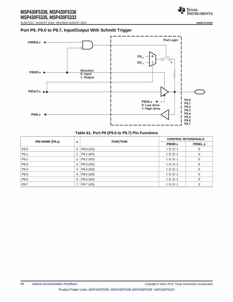
P9.0P9.1P9.2P9.3P9.4P9.5P9.6P9.7
Direction0: Input1: Output
P9DIR.x
P9IN.x
P9OUT.x
1
0DVSS
DVCC
P9REN.xPad Logic
1
P9DS.x0: Low drive1: High drive
MSP430F5338, MSP430F5336MSP430F5335, MSP430F5333SLAS721C –AUGUST 2010–REVISED AUGUST 2013 www.ti.com
Port P9, P9.0 to P9.7, Input/Output With Schmitt Trigger
Table 61. Port P9 (P9.0 to P9.7) Pin FunctionsCONTROL BITS/SIGNALS
PIN NAME (P9.x) x FUNCTIONP9DIR.x P9SEL.x
P9.0 0 P9.0 (I/O) I: 0; O: 1 0P9.1 1 P9.1 (I/O) I: 0; O: 1 0P9.2 2 P9.2 (I/O) I: 0; O: 1 0P9.3 3 P9.3 (I/O) I: 0; O: 1 0P9.4 4 P9.4 (I/O) I: 0; O: 1 0P9.5 5 P9.5 (I/O) I: 0; O: 1 0P9.6 6 P9.6 (I/O) I: 0; O: 1 0P9.7 7 P9.7 (I/O) I: 0; O: 1 0
94 Submit Documentation Feedback Copyright © 2010–2013, Texas Instruments Incorporated
Product Folder Links: MSP430F5338 MSP430F5336 MSP430F5335 MSP430F5333

PUOPE
PUOUT0
Pad Logic
PU.0
LDOO VSSU
PU.1PUOUT1
PUIN1
PUIN0
PUIPE
MSP430F5338, MSP430F5336MSP430F5335, MSP430F5333
www.ti.com SLAS721C –AUGUST 2010–REVISED AUGUST 2013
Port PU.0, PU.1 Ports
Table 62. Port PU.0, PU.1 Output FunctionsCONTROL BITS PIN NAME
FUNCTIONPUSEL PUDIR PUOUT1 PUOUT0 PU.1 PU.0
0 0 X X Hi-Z Hi-Z Outputs off0 1 0 0 0 0 Outputs enabled0 1 0 1 0 1 Outputs enabled0 1 1 0 1 0 Outputs enabled0 1 1 1 1 1 Outputs enabled
Copyright © 2010–2013, Texas Instruments Incorporated Submit Documentation Feedback 95
Product Folder Links: MSP430F5338 MSP430F5336 MSP430F5335 MSP430F5333
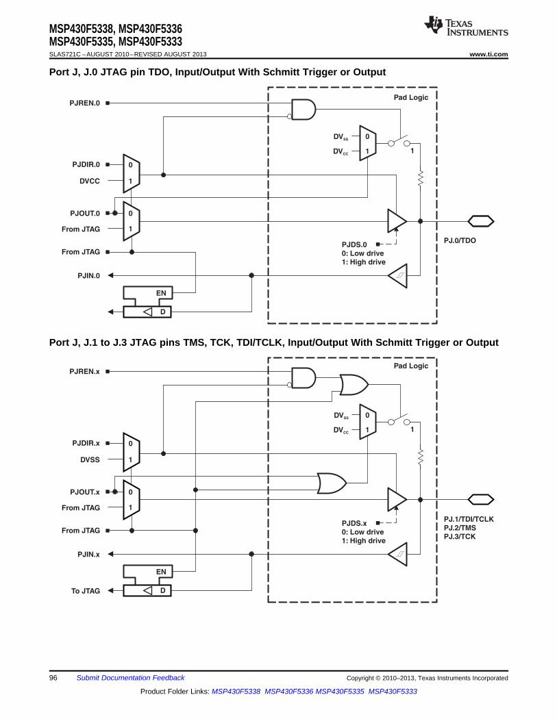
PJ.1/TDI/TCLKPJ.2/TMSPJ.3/TCK
From JTAG
1
0PJDIR.x
PJIN.x
EN
1
0
From JTAG
PJOUT.x
1
0DVSS
DVCC
PJREN.xPad Logic
1
PJDS.x0: Low drive1: High drive
D
DVSS
To JTAG
PJ.0/TDO
From JTAG
1
0PJDIR.0
PJIN.0
EN
1
0
From JTAG
PJOUT.0
1
0DVSS
DVCC
PJREN.0Pad Logic
1
PJDS.00: Low drive1: High drive
D
DVCC
MSP430F5338, MSP430F5336MSP430F5335, MSP430F5333SLAS721C –AUGUST 2010–REVISED AUGUST 2013 www.ti.com
Port J, J.0 JTAG pin TDO, Input/Output With Schmitt Trigger or Output
Port J, J.1 to J.3 JTAG pins TMS, TCK, TDI/TCLK, Input/Output With Schmitt Trigger or Output
96 Submit Documentation Feedback Copyright © 2010–2013, Texas Instruments Incorporated
Product Folder Links: MSP430F5338 MSP430F5336 MSP430F5335 MSP430F5333
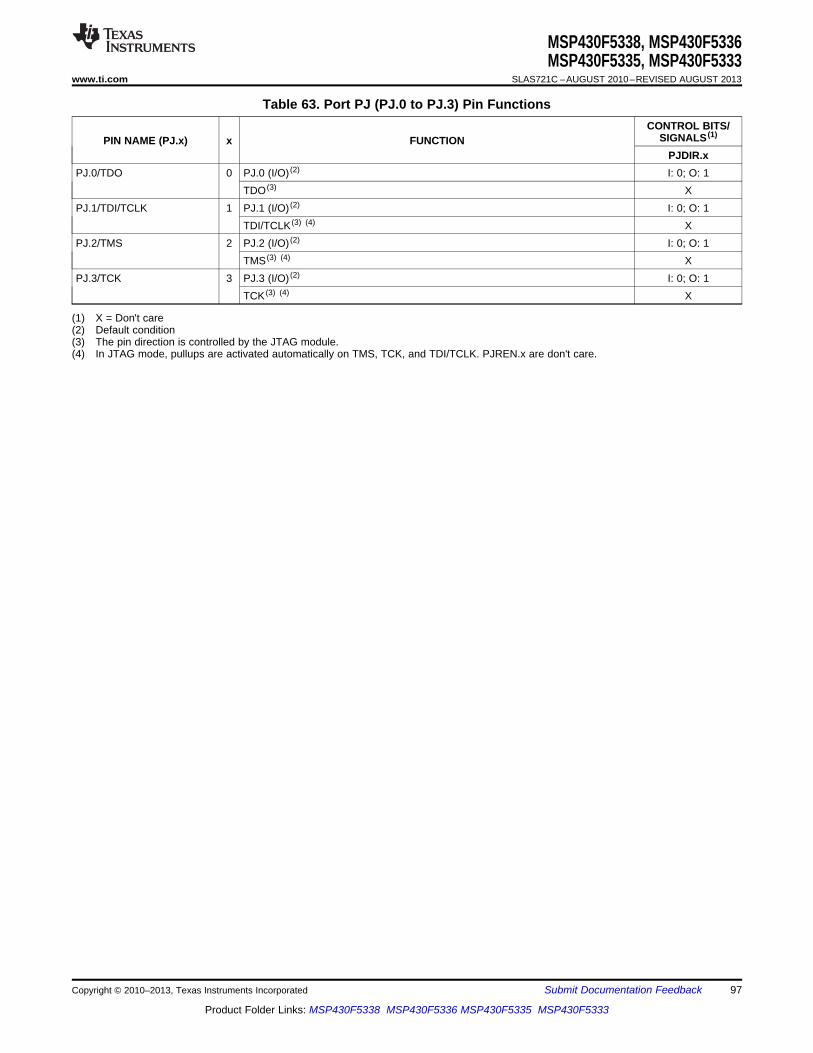
MSP430F5338, MSP430F5336MSP430F5335, MSP430F5333
www.ti.com SLAS721C –AUGUST 2010–REVISED AUGUST 2013
Table 63. Port PJ (PJ.0 to PJ.3) Pin FunctionsCONTROL BITS/
SIGNALS (1)PIN NAME (PJ.x) x FUNCTIONPJDIR.x
PJ.0/TDO 0 PJ.0 (I/O) (2) I: 0; O: 1TDO (3) X
PJ.1/TDI/TCLK 1 PJ.1 (I/O) (2) I: 0; O: 1TDI/TCLK (3) (4) X
PJ.2/TMS 2 PJ.2 (I/O) (2) I: 0; O: 1TMS (3) (4) X
PJ.3/TCK 3 PJ.3 (I/O) (2) I: 0; O: 1TCK (3) (4) X
(1) X = Don't care(2) Default condition(3) The pin direction is controlled by the JTAG module.(4) In JTAG mode, pullups are activated automatically on TMS, TCK, and TDI/TCLK. PJREN.x are don't care.
Copyright © 2010–2013, Texas Instruments Incorporated Submit Documentation Feedback 97
Product Folder Links: MSP430F5338 MSP430F5336 MSP430F5335 MSP430F5333
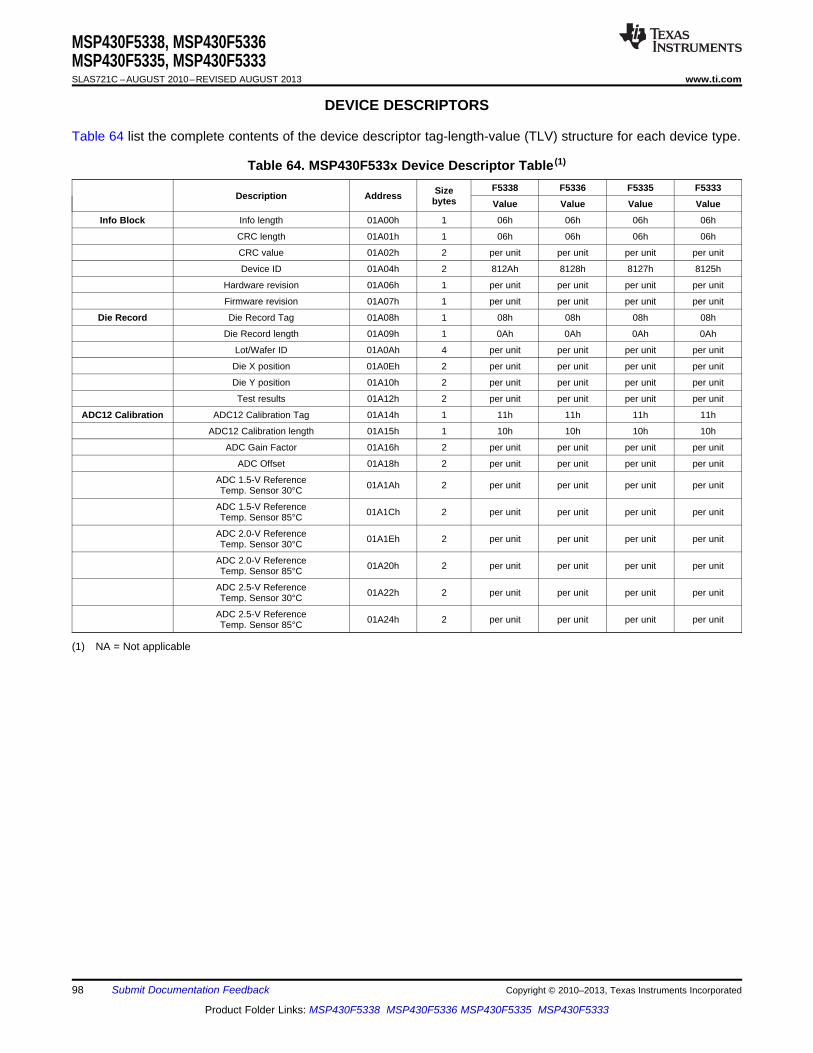
MSP430F5338, MSP430F5336MSP430F5335, MSP430F5333SLAS721C –AUGUST 2010–REVISED AUGUST 2013 www.ti.com
DEVICE DESCRIPTORS
Table 64 list the complete contents of the device descriptor tag-length-value (TLV) structure for each device type.
Table 64. MSP430F533x Device Descriptor Table (1)
F5338 F5336 F5335 F5333SizeDescription Address bytes Value Value Value Value
Info Block Info length 01A00h 1 06h 06h 06h 06h
CRC length 01A01h 1 06h 06h 06h 06h
CRC value 01A02h 2 per unit per unit per unit per unit
Device ID 01A04h 2 812Ah 8128h 8127h 8125h
Hardware revision 01A06h 1 per unit per unit per unit per unit
Firmware revision 01A07h 1 per unit per unit per unit per unit
Die Record Die Record Tag 01A08h 1 08h 08h 08h 08h
Die Record length 01A09h 1 0Ah 0Ah 0Ah 0Ah
Lot/Wafer ID 01A0Ah 4 per unit per unit per unit per unit
Die X position 01A0Eh 2 per unit per unit per unit per unit
Die Y position 01A10h 2 per unit per unit per unit per unit
Test results 01A12h 2 per unit per unit per unit per unit
ADC12 Calibration ADC12 Calibration Tag 01A14h 1 11h 11h 11h 11h
ADC12 Calibration length 01A15h 1 10h 10h 10h 10h
ADC Gain Factor 01A16h 2 per unit per unit per unit per unit
ADC Offset 01A18h 2 per unit per unit per unit per unit
ADC 1.5-V Reference 01A1Ah 2 per unit per unit per unit per unitTemp. Sensor 30°C
ADC 1.5-V Reference 01A1Ch 2 per unit per unit per unit per unitTemp. Sensor 85°C
ADC 2.0-V Reference 01A1Eh 2 per unit per unit per unit per unitTemp. Sensor 30°C
ADC 2.0-V Reference 01A20h 2 per unit per unit per unit per unitTemp. Sensor 85°C
ADC 2.5-V Reference 01A22h 2 per unit per unit per unit per unitTemp. Sensor 30°C
ADC 2.5-V Reference 01A24h 2 per unit per unit per unit per unitTemp. Sensor 85°C
(1) NA = Not applicable
98 Submit Documentation Feedback Copyright © 2010–2013, Texas Instruments Incorporated
Product Folder Links: MSP430F5338 MSP430F5336 MSP430F5335 MSP430F5333
MSP430F5338, MSP430F5336MSP430F5335, MSP430F5333
www.ti.com SLAS721C –AUGUST 2010–REVISED AUGUST 2013
REVISION HISTORY
REVISION COMMENTSSLAS721 Product Preview release
SLAS721A Production Data release
Changed description of ACLK in Terminal Functions.Added missing rows for DVSS and DNC (PW pins 29 and 30) in Terminal Functions.Changed typos to Interrupt Flag names on Timer TA2 rows in Table 5.Changed SYSRSTIV, System Reset offset 1Ch to Reserved in Table 12.
SLAS721B Corrected names of SVMLVLRIFG and SVMHVLRIFG bits in Table 12.Changed notes on REF, Built-In Reference.Changed tSENSOR(sample) MIN to 100 µs in 12-Bit ADC, Temperature Sensor and Built-In VMID.Changed note (2) in 12-Bit ADC, Temperature Sensor and Built-In VMID.Editorial changes throughout.
Table 2, Added note regarding pullup resistor to RST/NMI/SBWTDIO pin.Added Applications, Development Tools Support, and Device and Development Tool Nomenclature.Digital I/O (Link to User's Guide), Changed the description of the number of I/Os in each port.SLAS721CTable 20, Added PM5CTL0 register.12-Bit DAC, Supply Specifications, Fixed typo in IDD Test Conditions (changed from DAC12IOG to DAC12OG).Flash Memory, Changed IERASE and IMERASE, IBANK limits.
Copyright © 2010–2013, Texas Instruments Incorporated Submit Documentation Feedback 99
Product Folder Links: MSP430F5338 MSP430F5336 MSP430F5335 MSP430F5333
PACKAGE OPTION ADDENDUM
www.ti.com 2-Dec-2014
Addendum-Page 1
PACKAGING INFORMATION
Orderable Device Status(1)
Package Type PackageDrawing
Pins PackageQty
Eco Plan(2)
Lead/Ball Finish(6)
MSL Peak Temp(3)
Op Temp (°C) Device Marking(4/5)
Samples
MSP430F5333IPZ ACTIVE LQFP PZ 100 90 Green (RoHS& no Sb/Br)
CU NIPDAU Level-3-260C-168 HR -40 to 85 M430F5333
MSP430F5333IPZR ACTIVE LQFP PZ 100 1000 Green (RoHS& no Sb/Br)
CU NIPDAU Level-3-260C-168 HR -40 to 85 M430F5333
MSP430F5333IZQWR ACTIVE BGAMICROSTAR
JUNIOR
ZQW 113 2500 Green (RoHS& no Sb/Br)
SNAGCU Level-3-260C-168 HR -40 to 85 M430F5333
MSP430F5333IZQWT NRND BGAMICROSTAR
JUNIOR
ZQW 113 250 Green (RoHS& no Sb/Br)
SNAGCU Level-3-260C-168 HR -40 to 85 M430F5333
MSP430F5335IPZ ACTIVE LQFP PZ 100 90 Green (RoHS& no Sb/Br)
CU NIPDAU Level-3-260C-168 HR -40 to 85 M430F5335
MSP430F5335IPZR ACTIVE LQFP PZ 100 1000 Green (RoHS& no Sb/Br)
CU NIPDAU Level-3-260C-168 HR -40 to 85 M430F5335
MSP430F5335IZQWR ACTIVE BGAMICROSTAR
JUNIOR
ZQW 113 2500 Green (RoHS& no Sb/Br)
SNAGCU Level-3-260C-168 HR -40 to 85 M430F5335
MSP430F5335IZQWT ACTIVE BGAMICROSTAR
JUNIOR
ZQW 113 250 Green (RoHS& no Sb/Br)
SNAGCU Level-3-260C-168 HR -40 to 85 M430F5335
MSP430F5336IPZ ACTIVE LQFP PZ 100 90 Green (RoHS& no Sb/Br)
CU NIPDAU Level-3-260C-168 HR -40 to 85 M430F5336
MSP430F5336IPZR ACTIVE LQFP PZ 100 1000 Green (RoHS& no Sb/Br)
CU NIPDAU Level-3-260C-168 HR -40 to 85 M430F5336
MSP430F5336IZQWR ACTIVE BGAMICROSTAR
JUNIOR
ZQW 113 2500 Green (RoHS& no Sb/Br)
SNAGCU Level-3-260C-168 HR -40 to 85 M430F5336
MSP430F5336IZQWT NRND BGAMICROSTAR
JUNIOR
ZQW 113 250 Green (RoHS& no Sb/Br)
SNAGCU Level-3-260C-168 HR -40 to 85 M430F5336
MSP430F5338IPZ ACTIVE LQFP PZ 100 90 Green (RoHS& no Sb/Br)
CU NIPDAU Level-3-260C-168 HR M430F5338
MSP430F5338IPZR ACTIVE LQFP PZ 100 1000 Green (RoHS& no Sb/Br)
CU NIPDAU Level-3-260C-168 HR M430F5338
PACKAGE OPTION ADDENDUM
www.ti.com 2-Dec-2014
Addendum-Page 2
Orderable Device Status(1)
Package Type PackageDrawing
Pins PackageQty
Eco Plan(2)
Lead/Ball Finish(6)
MSL Peak Temp(3)
Op Temp (°C) Device Marking(4/5)
Samples
MSP430F5338IZQWR ACTIVE BGAMICROSTAR
JUNIOR
ZQW 113 2500 Green (RoHS& no Sb/Br)
SNAGCU Level-3-260C-168 HR M430F5338
MSP430F5338IZQWT ACTIVE BGAMICROSTAR
JUNIOR
ZQW 113 250 Green (RoHS& no Sb/Br)
SNAGCU Level-3-260C-168 HR M430F5338
(1) The marketing status values are defined as follows:ACTIVE: Product device recommended for new designs.LIFEBUY: TI has announced that the device will be discontinued, and a lifetime-buy period is in effect.NRND: Not recommended for new designs. Device is in production to support existing customers, but TI does not recommend using this part in a new design.PREVIEW: Device has been announced but is not in production. Samples may or may not be available.OBSOLETE: TI has discontinued the production of the device.
(2) Eco Plan - The planned eco-friendly classification: Pb-Free (RoHS), Pb-Free (RoHS Exempt), or Green (RoHS & no Sb/Br) - please check http://www.ti.com/productcontent for the latest availabilityinformation and additional product content details.TBD: The Pb-Free/Green conversion plan has not been defined.Pb-Free (RoHS): TI's terms "Lead-Free" or "Pb-Free" mean semiconductor products that are compatible with the current RoHS requirements for all 6 substances, including the requirement thatlead not exceed 0.1% by weight in homogeneous materials. Where designed to be soldered at high temperatures, TI Pb-Free products are suitable for use in specified lead-free processes.Pb-Free (RoHS Exempt): This component has a RoHS exemption for either 1) lead-based flip-chip solder bumps used between the die and package, or 2) lead-based die adhesive used betweenthe die and leadframe. The component is otherwise considered Pb-Free (RoHS compatible) as defined above.Green (RoHS & no Sb/Br): TI defines "Green" to mean Pb-Free (RoHS compatible), and free of Bromine (Br) and Antimony (Sb) based flame retardants (Br or Sb do not exceed 0.1% by weightin homogeneous material)
(3) MSL, Peak Temp. - The Moisture Sensitivity Level rating according to the JEDEC industry standard classifications, and peak solder temperature.
(4) There may be additional marking, which relates to the logo, the lot trace code information, or the environmental category on the device.
(5) Multiple Device Markings will be inside parentheses. Only one Device Marking contained in parentheses and separated by a "~" will appear on a device. If a line is indented then it is a continuationof the previous line and the two combined represent the entire Device Marking for that device.
(6) Lead/Ball Finish - Orderable Devices may have multiple material finish options. Finish options are separated by a vertical ruled line. Lead/Ball Finish values may wrap to two lines if the finishvalue exceeds the maximum column width.
Important Information and Disclaimer:The information provided on this page represents TI's knowledge and belief as of the date that it is provided. TI bases its knowledge and belief on informationprovided by third parties, and makes no representation or warranty as to the accuracy of such information. Efforts are underway to better integrate information from third parties. TI has taken andcontinues to take reasonable steps to provide representative and accurate information but may not have conducted destructive testing or chemical analysis on incoming materials and chemicals.TI and TI suppliers consider certain information to be proprietary, and thus CAS numbers and other limited information may not be available for release.
PACKAGE OPTION ADDENDUM
www.ti.com 2-Dec-2014
Addendum-Page 3
In no event shall TI's liability arising out of such information exceed the total purchase price of the TI part(s) at issue in this document sold by TI to Customer on an annual basis.
TAPE AND REEL INFORMATION
*All dimensions are nominal
Device PackageType
PackageDrawing
Pins SPQ ReelDiameter
(mm)
ReelWidth
W1 (mm)
A0(mm)
B0(mm)
K0(mm)
P1(mm)
W(mm)
Pin1Quadrant
MSP430F5333IZQWR BGA MI CROSTA
R JUNI OR
ZQW 113 2500 330.0 16.4 7.3 7.3 1.5 12.0 16.0 Q1
MSP430F5333IZQWT BGA MI CROSTA
R JUNI OR
ZQW 113 250 330.0 16.4 7.3 7.3 1.5 12.0 16.0 Q1
MSP430F5335IZQWR BGA MI CROSTA
R JUNI OR
ZQW 113 2500 330.0 16.4 7.3 7.3 1.5 12.0 16.0 Q1
MSP430F5335IZQWT BGA MI CROSTA
R JUNI OR
ZQW 113 250 330.0 16.4 7.3 7.3 1.5 12.0 16.0 Q1
MSP430F5336IZQWR BGA MI CROSTA
R JUNI OR
ZQW 113 2500 330.0 16.4 7.3 7.3 1.5 12.0 16.0 Q1
MSP430F5336IZQWT BGA MI CROSTA
R JUNI
ZQW 113 250 330.0 16.4 7.3 7.3 1.5 12.0 16.0 Q1
PACKAGE MATERIALS INFORMATION
www.ti.com 1-Apr-2014
Pack Materials-Page 1
Device PackageType
PackageDrawing
Pins SPQ ReelDiameter
(mm)
ReelWidth
W1 (mm)
A0(mm)
B0(mm)
K0(mm)
P1(mm)
W(mm)
Pin1Quadrant
OR
MSP430F5338IZQWR BGA MI CROSTA
R JUNI OR
ZQW 113 2500 330.0 16.4 7.3 7.3 1.5 12.0 16.0 Q1
MSP430F5338IZQWT BGA MI CROSTA
R JUNI OR
ZQW 113 250 330.0 16.4 7.3 7.3 1.5 12.0 16.0 Q1
*All dimensions are nominal
Device Package Type Package Drawing Pins SPQ Length (mm) Width (mm) Height (mm)
MSP430F5333IZQWR BGA MICROSTARJUNIOR
ZQW 113 2500 336.6 336.6 28.6
MSP430F5333IZQWT BGA MICROSTARJUNIOR
ZQW 113 250 336.6 336.6 28.6
MSP430F5335IZQWR BGA MICROSTARJUNIOR
ZQW 113 2500 336.6 336.6 28.6
MSP430F5335IZQWT BGA MICROSTARJUNIOR
ZQW 113 250 336.6 336.6 28.6
MSP430F5336IZQWR BGA MICROSTARJUNIOR
ZQW 113 2500 336.6 336.6 28.6
MSP430F5336IZQWT BGA MICROSTAR ZQW 113 250 336.6 336.6 28.6
PACKAGE MATERIALS INFORMATION
www.ti.com 1-Apr-2014
Pack Materials-Page 2
Device Package Type Package Drawing Pins SPQ Length (mm) Width (mm) Height (mm)
JUNIOR
MSP430F5338IZQWR BGA MICROSTARJUNIOR
ZQW 113 2500 336.6 336.6 28.6
MSP430F5338IZQWT BGA MICROSTARJUNIOR
ZQW 113 250 336.6 336.6 28.6
PACKAGE MATERIALS INFORMATION
www.ti.com 1-Apr-2014
Pack Materials-Page 3


MECHANICAL DATA
MTQF013A – OCTOBER 1994 – REVISED DECEMBER 1996
1POST OFFICE BOX 655303 • DALLAS, TEXAS 75265
PZ (S-PQFP-G100) PLASTIC QUAD FLATPACK
4040149/B 11/96
50
26 0,13 NOM
Gage Plane
0,25
0,450,75
0,05 MIN
0,27
51
25
75
1
12,00 TYP
0,17
76
100
SQ
SQ15,8016,20
13,80
1,351,45
1,60 MAX
14,20
0°–7°
Seating Plane
0,08
0,50 M0,08
NOTES: A. All linear dimensions are in millimeters.B. This drawing is subject to change without notice.C. Falls within JEDEC MS-026
IMPORTANT NOTICETexas Instruments Incorporated and its subsidiaries (TI) reserve the right to make corrections, enhancements, improvements and otherchanges to its semiconductor products and services per JESD46, latest issue, and to discontinue any product or service per JESD48, latestissue. Buyers should obtain the latest relevant information before placing orders and should verify that such information is current andcomplete. All semiconductor products (also referred to herein as “components”) are sold subject to TI’s terms and conditions of salesupplied at the time of order acknowledgment.TI warrants performance of its components to the specifications applicable at the time of sale, in accordance with the warranty in TI’s termsand conditions of sale of semiconductor products. Testing and other quality control techniques are used to the extent TI deems necessaryto support this warranty. Except where mandated by applicable law, testing of all parameters of each component is not necessarilyperformed.TI assumes no liability for applications assistance or the design of Buyers’ products. Buyers are responsible for their products andapplications using TI components. To minimize the risks associated with Buyers’ products and applications, Buyers should provideadequate design and operating safeguards.TI does not warrant or represent that any license, either express or implied, is granted under any patent right, copyright, mask work right, orother intellectual property right relating to any combination, machine, or process in which TI components or services are used. Informationpublished by TI regarding third-party products or services does not constitute a license to use such products or services or a warranty orendorsement thereof. Use of such information may require a license from a third party under the patents or other intellectual property of thethird party, or a license from TI under the patents or other intellectual property of TI.Reproduction of significant portions of TI information in TI data books or data sheets is permissible only if reproduction is without alterationand is accompanied by all associated warranties, conditions, limitations, and notices. TI is not responsible or liable for such altereddocumentation. Information of third parties may be subject to additional restrictions.Resale of TI components or services with statements different from or beyond the parameters stated by TI for that component or servicevoids all express and any implied warranties for the associated TI component or service and is an unfair and deceptive business practice.TI is not responsible or liable for any such statements.Buyer acknowledges and agrees that it is solely responsible for compliance with all legal, regulatory and safety-related requirementsconcerning its products, and any use of TI components in its applications, notwithstanding any applications-related information or supportthat may be provided by TI. Buyer represents and agrees that it has all the necessary expertise to create and implement safeguards whichanticipate dangerous consequences of failures, monitor failures and their consequences, lessen the likelihood of failures that might causeharm and take appropriate remedial actions. Buyer will fully indemnify TI and its representatives against any damages arising out of the useof any TI components in safety-critical applications.In some cases, TI components may be promoted specifically to facilitate safety-related applications. With such components, TI’s goal is tohelp enable customers to design and create their own end-product solutions that meet applicable functional safety standards andrequirements. Nonetheless, such components are subject to these terms.No TI components are authorized for use in FDA Class III (or similar life-critical medical equipment) unless authorized officers of the partieshave executed a special agreement specifically governing such use.Only those TI components which TI has specifically designated as military grade or “enhanced plastic” are designed and intended for use inmilitary/aerospace applications or environments. Buyer acknowledges and agrees that any military or aerospace use of TI componentswhich have not been so designated is solely at the Buyer's risk, and that Buyer is solely responsible for compliance with all legal andregulatory requirements in connection with such use.TI has specifically designated certain components as meeting ISO/TS16949 requirements, mainly for automotive use. In any case of use ofnon-designated products, TI will not be responsible for any failure to meet ISO/TS16949.Products ApplicationsAudio www.ti.com/audio Automotive and Transportation www.ti.com/automotiveAmplifiers amplifier.ti.com Communications and Telecom www.ti.com/communicationsData Converters dataconverter.ti.com Computers and Peripherals www.ti.com/computersDLP® Products www.dlp.com Consumer Electronics www.ti.com/consumer-appsDSP dsp.ti.com Energy and Lighting www.ti.com/energyClocks and Timers www.ti.com/clocks Industrial www.ti.com/industrialInterface interface.ti.com Medical www.ti.com/medicalLogic logic.ti.com Security www.ti.com/securityPower Mgmt power.ti.com Space, Avionics and Defense www.ti.com/space-avionics-defenseMicrocontrollers microcontroller.ti.com Video and Imaging www.ti.com/videoRFID www.ti-rfid.comOMAP Applications Processors www.ti.com/omap TI E2E Community e2e.ti.comWireless Connectivity www.ti.com/wirelessconnectivity
Mailing Address: Texas Instruments, Post Office Box 655303, Dallas, Texas 75265Copyright © 2014, Texas Instruments Incorporated