Embed Size (px)
Citation preview
MITSOBISBI
5 l/4- FLEXIBLE DISK DRIVE
MODEL M4853
OEM MANUAL
TJ2-G30213 A 9/83

_ _ •.•.•. _ ........ __ ._ ............. - •.• _~ .. _IW'_""" .... ,, ____ ''''\\''''\\\\\\\\\\\\\\\,,\\\\\\\\\\\\Mf I »UIII5HI ELLC'TRtC
" ."'., l.....-"
M4853·1 flu."ble Disk Driye

.' " .. A~""~~"""'~"~"~~"\~\~-~~~~""\~""~~"~""\\~~~\\\\\\~MrrsuBlSHl ELECTRIC
1.1 1.2 1.2.1 1.2.2 1.2.3 1.2." 1.2.5
2.
2. , 2.2 2.3 2.11 2.5
3.
3.1 3.2 3.3 3.11 3.5 3.6 3.7 3.8
II.
11.1 ".1.1 ".1.2 ".1.3 ".1." ".2 ... 2.1
""85"-1S OEM MANUAL
TABLE Of CONTENIS
INTRODUCTION •••.••••••••••••••••••••••••• 1_1
General Descr1ption •••••••••••••••••••••• 1-2 Specit1cations ••••••••••••••••••••••••••• 1-3
Pertormance Specs •••••••••••••••••••••• 1-3 Functional Specs ••••••••••••••••••••••• 1-.. Pbyslcal Specs ••••••••••••••••••••••••• 1-5 Environment.l Specs •••••••••••••••••••• 1-6 Reliability Specs •••••••••••••••••••••• 1-7
GE.EIAL OPEIATIO ••••••••••••••••••••••••• 2-1
Srstem Operat1on ••••••••••••••••••••••••• 2-1 Electronlcs •••••••••••••••••••••••••••••• 2-1 Rotation Hecbanlsm ••••••••••••••••••••••• 2-3 Positioning Hechanlsm •••••••••••••••••••• 2-3 le.d/Wrlte Heads ••••••••••••••••••••••••• 2-3
FUNCTIONAL OPERATION ••••••••••••••••••••• 3-1
Pover-On Sequenc1ng •••••••••••••••••••••• 3-1 Drive Selectlon •••••••••••••••••••••••••• 3-1 Positioning Operatlon •••••••••••••••••••• 3-1 Side Selectlon ••••••••••••••••••••••••••• 3-2 lead Operatlons •••••••••••••••••••••••••• 3-2 Write Operatlons ••••••••••••••••••••••••• 3-2 Dlsk Insertion ••••••••••••••••••••••••••• 3-3 Disk Removal ••••••••••••••••••••••••••••• 3-3
ELECTRICAL INTERFACE ••••••••••••••••••••• "-l Signal Intert.ce ........................... -3
C.bling Method .nd Input Termlnations .... -3 Llne Drives and Recelvers ................ -3 Input Slgnal L1nes ....................... -5 Output Slgnal L1nes ..................... -11
Power Intert.ce •••••••••• ~ •••••••••••• ~ ... -1 .. DC Power •••••••••••••••.••••••••••••••• --,,,
111

5.
5.1 5.2 5.3 5.&1
6.
6.1 6.2
7.
8.
8.1 S.1.1 8.1.2 8.1.3 8.2 8.3 8.3.1 8.3.2
9.
9.1 9.2
PHYSICAL INTERFACE ••••••••••••••••••••••• 5-1
S1gnal Connector ••••••••••••••••••••••••• 5-1 DC Power Connector •••••••••• ~ •••••••••••• 5-3 Frame Ground Connector ••••••.•••••••••••• 5-~ Interface Connector Locat1on ••••••• ~ ••••• 5-5
PHYSICAL SPECIFICATIONS ••••••••.••••••••• 6-1
Installat10n Or1entat1on ••••••••••••••••• 6-1 Dr1ve D1mensions ••••••••••••••••••••••••• 6-1
USER OPT10IS ••••••••••••••••••••••••••••• 7-1
.Drive Select Options ••••••••••••••••••••• 7-1 Motor Control Options ••••••••••••.•••••••• 7-2 Ready Output Opt1ons ••••••••••••••••••••• T-5 Head Load Opt1ons •••••••••••••••••••••••• 7-8 LED Opt1ons ••••••••••••••••••••••••••••• 7~'O Term1nat1ons •••••••••••••••••••••••••••• 7-12 Frame Ground ••••••••••••••••••• ~ •••••••• 7-12 Opt1ons Summary ••••••• ~ ••••••••••••••••• 7-13
RECORDING FORHAT ••••••••••••.••••••••••••• 8-1
Record1ng Encod1ng ••••••••••••••••••••••• 8-1 FH ••••••••••••••••••••••••••••••••••••• 8-2 MFH •••••••••••••••••••••••••••••••••••• 8-3 HHFH ••••••••••••••••••••••••••••••••••• 8-'1
Recommended Formatt1ng ••••••••••••••••••• 8-5 Error Detection and Correct1on •••••••••• 8.;.12
Write Errors •••••••••••••••••••••••••• 8-12 Read Er~ors ••••••••••••••••••••••••••• 8-12
SHIPPING •••••••••••••••••••••.•.••••••••. 9-1
Shipping Damage •••••••••••••••••••••••••• 9-1 Re-Sh 1pp1nl •••••••••••••.•••••••••..•... • ·9-1
tv

, . \ \\ \\ \ \
Li$t pf figyrc$
2-1 H~85q-1S Functional Diagram
3-1 Comparison of FH and HFH Encoding 3-2 Read/Write Drive Compatibility
q-1 Cab11nt Hethod q-2 Recommended L1ne Driver and Receiver C1rcuit 4-3 Dr1ve Select Timing q-~ Side Select Timing q-5 Step T1ming 4-7 Index T1ming 4-B Track 00 T1m1ng q-9 Bas1c Ready T1ming
5-1 Connector J1 Dimensions and P1n Numbers 5-2 Connector J2 5-3 Connector Locat1on D1agram
6-1 Disk Dr1ve Installation Directions 6~2 Dimensions of MQB5Q-1S
7-1 In-Use Latch Tim1ng 7-2 Current Ready (I) Timing 7-3 Held Ready (II) T1m1ng 7-q D1sk Change (Drive Select Reset) Timing 7-5 Disk Change (Step Pulse Reset) Timing 7-6 Head Load Opt1ons Schemat1c 7-7 Fr~me Croud Circu1t 7-B PCB Option Locat1ons
8-1 FH Wr1te T1m1ng B-2 FH Read T1m1ng 8-3 MFH Wr1te T1m1ng B-q MYH Read Timing B-5 HKFH Write T1ming 8-6 HHFH Read T1ming 8-7 ISO-7Q87/2 style, Track DO, Side 0 (FH) 8-8 ISO-7Q87/2 style, All other tracks (MFH) 8-9 512 Bytes/Sector, Standard Format 8-10 1,02Q Bytes/Sector, Standard Format 8-11 256 Bytes/Sector, S1mplif1ed For~at 8-12 512 Bytes/Sector, ~illp11f1ed Forn'at 8-13 256 Bytes/Sector, IEC 765A Format 8-1q 512 Bytes/Sector, IEC 765A Format 8-15 1,02- Bytes/Sector, IEC 765A Format
9-1 Head Protection sheet Installation 9-2 Bag and Board Assembly 9-3 Ten-Pack Carton Assellbly 9-~ S1ngle-Pack Carton Asse~bly
1v

List pf Tables
1-1 Performance Specifications 1-2 Funct10nal Specifications 1-3 Physical Specifications 1-4 Environmental Specifications 1-5 Reliability Specifications
4-1 DC Power Connector Pin Arrangement _-2 Signal Connector Pin Arrangement --3 DC Power Specifications
5-1 Connector for TWisted-Pair Cable (P1) 5-2 Connector for Flat Cable (P1) 5-3 DC Power Connectors
'1-1 Option Summary
y

1. INTRODUCTION
The K1tsub1sh1 K~85~-1S 1s a high-performance, double-sided, double bit and double track ~ens~ty flexible disk drive using a high-density 5.25-inch d1skette, that provides maximum customer ~~t~~raction with hlgh reliability and long service life.
- Main Features -
o Has an unformatted capacity of 1.6 mega-byte, and a transfer rate of 500 kbit/sec.
o Spindle speed can be selected from interface (360 RPM to 300 RPK). Changes disk capacity to 1.0 Kegabyte.
o Is compatible with the new IBH PC-AT (trademark of International Business Machines Corporation) Whigh capacity" floppy disk dr1ve, either w1th a 300 or 250 Kblt/second transfer rate.
o Is electrically compatible with 8" floppy disk drive controllers.
o LSI ICs have been used to reduce the size of the drive and 1~~rp~~p rpJiability.
o Easily removed front panel allows packaging flexibility.
o Includes'a diskette ejector for easy diskette removal.
o A circular gimbal spring 1n the read/write head suspension aechanism greatly improves med1um tracking performance.
o The steel band, flat stepping motor drive system for posit1on1ng achieves the best 1ntertrack access til;e in ~ts class: just 3 ms.
o The maintenance-free, DC, brushless, direct-drive motor obviates ttte bel t replacement necessary (or conventional counterparts.
o Excellent med1a interchangeab1lity, wide off-track window time Ita rgin, and hi tit ,.er (orl.ance are ma 1nta ined ove r wide ambient temperature and relative humid1ty ranges.
o The hlgh-torque sp1ndle Inotor permits control by s~itcbing on and off either the motor (starting t1me 500 illS) or the head load solenoid (loadine tll\e less than 50 liS).
o Dynam!c clamping insures correct disk seating w~th easy disk insertion.
1-1

.~
;...~~~'\~~~~~,,~'\~~~\~~~~\~--~,,\~~~~~~,,~,,~~~~~~""~,,~\~~~,,\~",\MITSU8tSHl ELECTRIC
, J
,., GENERAL DESCRIPTION
o The MQB5Q-1S Flexible Disk Drive 1s a t~in-head, double-~i ded. magnet! c disk dri ve with an unformated memory capa~lt) of 1.6 megabyte (360 RPM), or 1.0 megabyte (300 RPM), for doubledensity recordings.
o For 1.6 Megabye operation the K4B54-1S reads and wr1tes 5.25-1nch, double-s1ded high density dIskettes in double-density for~at.
o The fo;q 85Q- 1 S employs the unique Mi tsubi st,1 circular gimbal spring for holding and loading the magnetic heads to assure soft, steady contact with the aed1um. This lDeans elcellent read/write operation and a long service life for the medium. One of the outstanding features of this .echanism is reduction of the effects of jacket deforlhation and thickness variations, thereby &tabilizing read/write performance.
o By changing the data transfer rate and/or the spindle speed, and translating track numbers given to the controller, three different types of dl~~~ ma~ b~ acco~odat.€d:
A) 96 TPI, high density disks may be read and written without restriction.
B) 96 TPI, . standard density dlS~S "lay be read and written after changing either the transfer rate or the spindle speed.
C) .8 TPI, standard density disks may be read and written on, after changing the transfer rate or the spindle speed. Once written upon by the H4854-1S, the disk cannot be reliably used in a .8 TP1 disk drive again.
o The H4854-1S allows two methods of dOk~~6rd COli pit t 1 bil1 ty :
A) 360 RPM operation, with either 500 or 300 [bit/second transfer rates. A -low write current- input must be used to write on standard density .,dia.
The spindle speed IDay be lowered to 300 by use of an input to the drive. The transfer rate would be changed to 250 Kbit/second.
1-2

"
. J.... ~~,,~""~.""""\'\~~,,~_\'\~\~~~~~,,~~,,~\~""""""""~""\~~~"""~MrTSUBrSHt ELECTRIC
1.2 SPECIFICATIONS
, .2. , Performance specifications (Table 1-1)
Hemory capad ty
Unformatted
Disk, kilobytes
Per surface, kilobytes
Per track, ki.lobytes
Formatted
Disk, kilobytes
Per surface, kilobytes
Per track, bytes
(bytes/sector)
(sectors/track)
Transfer rate. Kbits/sec
Ave'rage la tency tilDe
Hot6r starting ti~e.nSec.max
Access time
Track to track
Iverage
Settling time
Head loading time
Speed change time
360 RPM 1.6 HB 1.0 HB
1664
832
10.11
1228.8
6'''.11
7680
(512)
(15)
500
83
500
1000
500
6.25
655.4
327.7
_096
(256)
(16)
300
83
500
3 mS maximum (unsettled)
300 RPM 1.0 HB
1000
500
6.25
655.11
327.7
" 096
(256 )
(16)
250
100
" 00
9" mS (including settling time)
15 mS maximum
50 mS maximum (including settling> .
400 nSec lIaxillum
Table 1-1 Performance Specifications
1-3

1.2.2 functional specifications (Table 1-2)
Magnetic flux inversion density
Encodin£. II'lethod
Track density
Number of cylinders
Humber of tracks
Number of heads
Rot.at.ion period
Index
Media
360 RPM 300 RPM 1.6 MB 1.0 MB 1.0MB
9870 5922 5922
9B70 FeI 5922 5922
MFM MFM Mn~
96 96 96
80 BO BO
160 160 160
2 2 2
166.7 £ 3.3 mSec
1
Double-sided 96 TPI, double densit.y, h1ghdensity 5.25 inches diskette, soft ~ect.ored
ExAmples:
Brown Disk Mfgr. Maxell Memorex BASF Dysan
UHR-2 MD2-HD 20-BO-HD HDFD UHR-2
Table 1-2 Funct.ional Specificat.ions
1-"
· ., ."

Physical specifications (Table 1-3)
.12 V
Heat dissipation
Physical dimensions
Height
Width
Depth
Front panel d1l1'1ensions
Height
Width
Weight
.. 5 V 51, 0 • 5 A t y pic a 1 ( seek i n g )
.12 V 51, 0.5 A typical (seeking)
8.5 watts typical, seeking
5.0 watts typical, reading in E-taf\dby DIode
t.O watts typical motor off
(Ex cept for front panel)
1.62 in (li 1 mm)
5.75 in (1"6 D!D'. )
7.68 in (195 Irm)
1.65 1n (lI2.0 mm)
5.83 in ( 146.0 mm)
2.9 lbs (1. 3 kg)
Table 1-3 Physical Specif1catjons
1-5

1.2.4 Environmental Specif1cat~ons (Table 1-~)
OperatinL ~nviron~enta' conditior.~ .
Ambient temperature
Relative humidity
Shock
Vibration
Altitude
Non-operating environmental conditions
Ambient temperature
Relative humidity
Shock
Vibration
Altitude
Transportation environment conditions (max 72 hours)
AmbiepL temperature
Relative Humidity
5 to 46 Deg. C (_1 F tc 115 F)
20S to 80S (Maximum wet bulb temperature: 29 C (85 F)
2.5 G Max (20 mSec)
0.25 G Max (5-200 Hz.)
-300 to 3000 meters
-20 to 51 Deg. C (-~ F to 125 F)
51 to 95S, non-condensir.&
30 G Max (20 mSec)
3.0 G Hax (5-200 Hz.)
-300 to 3000 meters
-40 to 62 Deg. C (-40 to 144 Deg. F)
11 to 951, non-condensing
Table 1-4 Environmental Specifications
1-6

"
1.2.5 Re11ab~11ty spec1ficetions (Table 1-5)
HTBF 10,000 POH (Power On Hours) minimum
~TTR 30 minutes
Unit life
Media life
Insertion
Rotational 11 fe
Tap-tap
Error rate
Soft read error
Hard read error
(Both hard and soft error rates assume a 100S open MF~ data and clock window, and 8 correctly operating phase-lock loop data separator)
Seek error
5 years or 20,000 energized hours, whichever comes first
~ 3 1 10 or more
6 3.5 x 10 pass/track or more
4 5 I 10 on the same spot of a track
-9 10 bit (2 retries)
-12 10 bit (10 retries)
-6 10 seek
Table 1-5 Reliability Specifications
1-7

· A~"""~""~~~"~"""~~~~",,,,~~~,,,,,,~,,~~~,,~~,,~,,\~~~~,,~~,,'\~,,~,,"~"~,\MrTSU81SHI ELECTRIC .'
1-8

.. 2. GENERAL OPER~TION
2.1 SYSTEM OPERATION
The H~85~-1S flexible Disk Drive consists of a mediun. rotatine mechanism, two read/write hea~s, an actuator to positio~ L~e read/write heads on tracks, a solenoid to load the read/write ~ead~ on the medium, electronic circuits to read and write data, and to drive these componel"ts.
The rotation ~echanism clamps the medium Inserted il"Lo the drive to the spindle, which j~ direetly coupled to the DC brushless motor. and rotates it at 360 or 300 RPM. n.e rosltloning actuator moves the read/write to be head over the desired track of the medium. Then, the head loading solel"ojd loads the read/write head on the medium to read or write data.
2.2 ELECTRONIC CIRCUITS
The electronic cIrcuits driving the individual mechanism.s of the "1&851&-15 are located on a single rrinted-circuit board, which consists of the following c1 rcul ts:
o Line driver and receiver that elchanees sitn.l~ with the host syste~ .
o Drive selection circuit
o Index detection circuit
. 0 Head positioning actuator drive circuit
o Head loadlne solenoid drive circuit
o Spindle motor control speed clrcu~t
o Read/write circuit
o Write protect circuit
o Hormal/low write current selection circuit
o Track 00 detection circuit
o Drive ready detection circuit
o Head selection circuit·
o In use indicator LED driye circuit 2-1

. ;... ~~\).~~"'\).~""\~\).\~~~~~~~\).\)'\)'\)'\)'\)'~\)'\~~"~""""\)'''\).\).\)'''~\).~~''''\~~MrTSUBlSHr EL.ECTRI~
READ DAn
WRITE CATE
WRITE DATA
'~RI TE PROTECT
SIDE SELtCT
IN USE
STEP
D I REC'I' I Ol~ SEU::.
OJUV£ SEL.i:CT
HIOEX
I1OJ'OR ON
READ CIRCUIT
WRITE CIRCUIT
CONTROL LOGIC
. READ/WRITE HEAD 0
READ/WRITE HEAD 1
""""--'-----'- '''RITE PROTECT DETECTOR ,------
INDEX LED
ACTIVITY LEO
DISK ...- -PRESENT
SWITCH
" INDEX DETECTOR .... -----------I I I I
CONTROL CIRCUIT
SPINDLE MOTOR ASSY --------~--------DC MOTOR I
I I I I I I I
I I L _____________ ~ ______________ ~
.
Figure 2-1 "qB5~-'S Functional Diagram 2-2

2.3 ROTATION MECHANISM
2.!l .
The di~~ette rotation ~echanism uses a DC brushless direct-drive motor to directly rotate the spi~o)e at 300 or 360 RPM.
POSITIONING t'.ECHA~ISH
The positioning mechanism is a high-performance ~t~~) band tYfr.
The head carriage assembly is fastened to the steel band which in turn is secured around the capstan of a two-phase hybrid s~epping motor; e 1.8 turn of the steppine ~otor moves the read/write ~ead one track in the designated direction, thus positioning the read/write head.
This drive syst.em is temperature cOIr;,lensat.ed t.o mibimize read/write head deviations from the disk t.racks caused by ambient temperature change.
2.5 READ/WRITE HEADS
The read/write heads use HnZn magnetic ferrite.
Eac~ read/writ.e heaG has three ferrite cores, co~~isting of a read/write core and erase cores on both sides of the read/write core to erase the space between tracks (tunnel erase).
The two read/write heads, which are located face-toface with the disk between them, are mounted er. compliant, circular gimb&l springs so that t.he heads track tt.e disk with good contact to enable Dlaxi mUD;
reproduction of the signals from the disk. The high surface tracking ability of the circular gimbal keeps the disk free of stress, and thus improves diskett~ I j fp..
2-3

.. . .

.'
3. FUNCTIONAL OPE~~!IO~
3.1 POWER ON SEQUENCING
No operation ~ay be performed for a period of 100 msec after the application of DC power to th~ drive.
The read/write head ~ay be positioned on an incorrect track after switching the DC power on, so before starting a read/write operation, perform a step out operation until a track 00 s1gnal is detected, thus correctl y posi t10nS ne. the t.ead at a known posi ti c 1'1.
3.2 DRIVE SELECTION
The M~B5~-'S daisy chain cabling system per~its conl'lection of multiple drives with a single cable.
These drives are selected when the drive select ljl'le~ from the control Ie r beCOD·e acti ve. Onl y . the dri ve who~e driVE ~elect line is active sends and receives signals to and from the ho~t system. The sele~t lines on the drives must have different numbers if two or more drive~ &re connected. If the same number is assigned, an operation error occurs due to interferenc£ alflone the output signals of tile drive~.
3.3 POSITIONING OPERATION
The seek operation .. hich 1J,0ve~ tite read/write head to t~e desired track selects a direction first, inward or outwa rd. wi th the pola ri ty . of Ule di rec tion s el ect signal; and ~oves the head with the step Signal. If access to a track two or more tracks away is required, step pulses are continuously sent until the head moves to the desired track.
Head movement occurs with the trailSne. ede.~ of t~e ~ter pulse.
sometimes write) a ~B TPI But U.e ~oftwa re DlJS t two -96 TPI- tracks for
It is allowable to read (and disk 1n a 96 TPI disk drive. command the controller to move one .B TPI track.
3-1

3.4 SIDE ONE SELECT10N
The read/write heads located on both sides of the diskette are selected by the side one select signal. When the side one select ljne is high, the side 0 head 1~ select~d. When ,t is low the side 1 head 1s selected. .
3.5 READ OPERATION
Three ~odes of encoding, FH, KFH, or HHFH are used for the data stored on ~~d1a. FH is used for singledensity recording, and HFH or KKFH for double-density recordir"e,.
The required timing of operations for reading is described in Chapters _ and 8.
A comparison of the FH and HFH encoding modes is shc~n in Fig. 3-1. See chapter B for a complete description of encoding ~ethods.
3.6 WRITE OPERATIONS
~rite data can be encoded by either FH, KFH, or HMFH. The Hq85~-'S has eood contact stability of the read/write heads on the medium and employs highperfor~ance read/write heads, so no precompensation is necessary for correcting the bit shift effect when writing data in the HFH ~ode (double density). However, if it is desired preco~pensation of 150 nSec or smaller should be used on tracks -3 and above, and none ~hould be used on lower numbered tracks.
When using the drive 1n a 300 or 250 K bit/second transfer rate mode no precompensation can be used. Doing so will only reduce the read data ~1ndow ~are1n~.
The requ1redt1m1ng of operations for reading is described 1n Chapters _ and 8. See chapter 8 for a complete description of encoding methods. See Fie,ure 3-2 for allowable read/write combinations between different types of drives.
3-2

.' 3.7 DISK INSE~')O~
"~e sequence of events that occur with disk 1n~E'rti(lrl e r t' :
l' Tre user insert~ the disk into the drive ~nt!l audible "click" 1s heard. Tids indicates thilt tt,t' drive ejection mechanism has received the dis~.
2) When the disk js fully 1~serted 1nto the drive, a mechanical sw1tct. is actuated, and the spindle ~otor start~ to rotate.
3) The user clamps the disk on to the rotatinE spindle using the bridge handle. Tt"le t'CI~dle is moved until an audible click is heard.
4) The disk starts to rotate, and the index sensor beg1ns to detect pulses 'of light from Ute index LED.
5) The index pulses are deteced 1n a E1nimum period of t1me, which switches the -held ready" 10g1c to a true state. (If the disk 1s ~ properly seated, this will not. occur because the index hole in the disk w111 never aJlo~ light to ~trjke the presise location requ1red to activate the photo-transistor that is the index pulse sensor.) The spl~dle ~tor is turned off.
6) Option JUII·per He may be used to load the head on to the disk at this time. This 1s desirable if the user wishes to el1minate the head load and settling th';es associated with D:>tor start/stop operation.
3.~ DISK REMOVAL
To remove the disk from the dr1ve the user depresses tt'E: front panel door flap, vh ich releases the br 1d ge handle. The ejector mechanism then transports U.e disk out of the drive into the users fingers.
This action a1,so resets the "held ready" status to a false condit10n, or the -disk change" status to a true condition, which can be detected by having the system control Ie r poll the dd ve for Its st.atus.
3-3

.. J A*,""""~~"~,,~~~~~,,~~~~~~~,,~~\~~~~~~~~~~\~~~~\~\~~~~~~~,,"~""~~~~~~~~~~'MrTS~lEaSHI ELEcTRIC
FM
J2rL I , I , I , I
1 o
DATA i 1 11 I 1 I 0 I 1 I 0 I 0 I 0 I 1 I I I
JoCF11'
1
,/ ,/
,/ /
o
/ ,/
/ ,/
,/ ,/
/
o
/ /
/
,/ /
1
/ ,/
,/
Figure 3-1 Comparison of FH and MFH Encodif'l£ 3-11

'" '" -.... .. I
P\ ... i
~ :: S ... ;1 ... ~ .. ... ! i' - " w i .. E .. ~ D
a c u
~ ::: • " i
DISCL'TTt WI! IT1T.I/ It "IIS D"'tl'OOt
M8~1
~:.';: :no nl5ec JOO Or .... l.
C.~fIB [X 41 ~I
250 h!Sec JOOOr .......
o.~
41 "I lIou (l) YES 250 .MSec JOOOr ....
1.0 fIB t6 "I
10 %50 l~/s.c: JOOCIt ....
O.S Ie 41 TPI rES IIot. (I) lIOO n/Sec lIOOOr ....
1.0 Ie t6 TPI II)
JOO n/s.c: JOOOr ....
1.6..e 96 "I
II)
500 1~15ec 6OO·Or ....
O.S Ie 611 TPI lIou <'I rES 250 n/s.c: JOO Or twr.
1.0 Ie
" TPI II) IIot~ (5) %s.> I ~/s.c: JOOOr IWY
1.6 .. 96 TPI 110
500 1~15ec 600 Or ....
MIS] MI!IoIo-IIJ1
~:~- l;O"te g.) N 1:0 fIB 1.6 fIB 4' "'I t6 "I " "'I t6 "I t6 "I lIou (I) IIol~ (2) lIou U) :no n/s.c 250 hfMc JOO h!Wc JOO l~~ 500 1~15ec JOO 0.. fIodaa JOOO" .... )00 Or fIodaa JOO Or 600 0.. ....
II) II) 110 II) II)
[>( II) m 10 II)
110 t>< 110 n:s II)
m
110
110
YES
10
110
10 [>( 10 10
YES II) [X II)
II) II) 110 [>( 10 YES 110 II)
ns 110 IES 10
II) 10 10 m
MiltS
I. n.e" TPJ he" _t .... "~1e at.,.,..., c_uoller
2. n.e" TPI ..... _t ... ·"~I . .u~., c_troll.r. IIIrlu c.r .. t _I ...
""IOCH. S. ""ite urr.a, _t ... rMc". ,. n.e" "'1 ~ _t ... • ... ~l. K."....
., c_tron.r. S.-4 rw4«M ta lIOO ..... S. Speo4 rHOOCH ta XIO .....
M8!101o-lIlS
o.~ Ie 1.0 fIB 61 TPI t6 "'I lIou (4) lIou U)
250 l~~ JOO Or
250 l~'~ JOO 0..
II) II)
YES . II)
II) rES
ns 10
II) YES
10 II)
[>( 110
II) [X II) II)
Figure 3-2 Read/Write Drive Compatibility 3-5
1.6 tQ!
96 "'I
500 I~'s:.. 6OOOr..b..
110
II)
II)
II)
II)
rES
II)
II)
[>(

'.
3-6

~. ELECTRICAL INTERFACE
There are two kinds of electrical interfaces: and DC power interface.
Signal interface
The signal interface ~e~ds and receives control signals and read/write data between the M485~-1S and the host syste~ via the J1/P1 connector.
The DC power interface drives the spindle drive Ir.otor of tile M4854-1S, and supplies power to the electronic circuits a~ci tt'E: stepping motor which drives the read/~rite head positionine mechanislr. via the J2/P2 connector.
The signals and pin arrangement of these two types of 1nterfac~~ are shown in Tables 3-1 and 3-2.
Source voltaee Pin number
.12 V DC 1
.12 V DC return 2
.5 V DC return 3
+5 V DC
Table ~-1 DC Power Connector Pin Assign~ents (J2/P2)
~-,
Signal
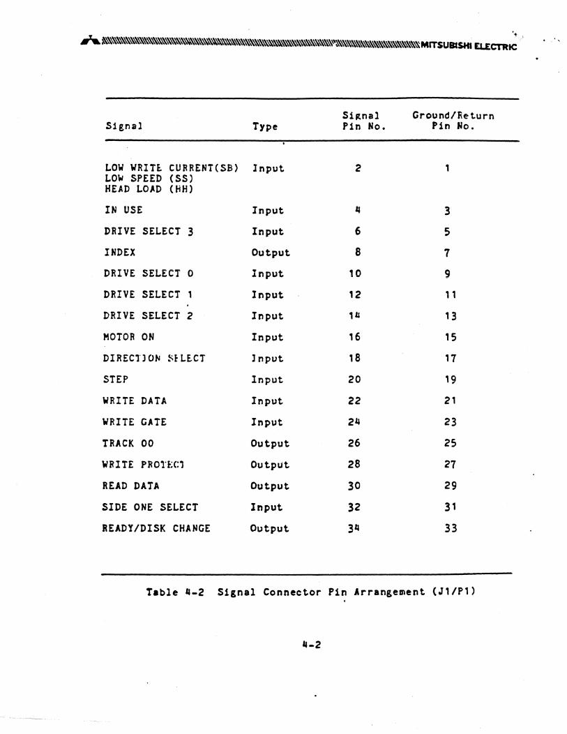
LOW WRITE. CURRENT(SB) LO~ SPEED (SS) HEAD LO'(D (HH)
IN USE
DRIVE SELECT 3
INDEX
DRIVE SELECT 0
DRIVE SELECT 1
DRIVE SELECT 2
MOTOR ON
DIRECnOt.l M LE.CT
STEP
WRITE DATA
WRITE GATE
TRACK 00
WRITE PROl"U:1
READ DATA
SIDE ONE SELECT
READY/DISK CHANGE
Type
Input
Input
Input
Output
Input
Input
Input
Input
Input
Input
Input
Input
Output
Output
Output
Input
Output
S1~nal Pin No.
2
14
6
8
10
12
1tl
16
18
20
22
214
26
28
30
32
3"
Ground/Return Pin No.
1
3
5
7
9
11
13
15
17
19
21
23
25
27
29
31
33
Table "-2 Signal Connector Pin Arrangement (J1/P1)

~., SIGNAL INTE~FAC[
~ . , . ,
". '.2
1he signal interface is classified into control signals 8~d d~La signal~. These interface signal lines are all at TTL levels. The meanings and characteristics of the ~1er.al levels are as follow~:
0 True = logic21 "0" = Vl 0 V to +0.1& V lin 110 mA Ir.aximum
0 False = loeical "1" = VH +2.5 V to 5.25 V lin 0 mA
0 Input impedance = 150 ohms
Cabling method and input line terminatio~
The ~~8511-1S uses a daisy chain cabling systelli. A single ribbon cable or twisted-pair cable may be fitted with multiple connectors to permit connection of up to fou.r dri ves.
The connected drive! are multiplex-controlled by drive select lines, and anyone of the drives can be accessed.
T~e cabling ~ethod and input line termination are shown in Fig. ~-,. A Daxi~uD'l of eight input signal lines, plus the drive ~elect line~. D8Y be terminated ~t the H~8511-'S. Proper operation of the drives requires termination at or near the drive connected to the end of the interface cable farthest from the host system.
The H~85~-'S has a resistor pack in a socket pr inted-ci rcui t boa rd to terlr,ina te these input li.nes.
on the si gnal
Wben a drive is shipped from the factory, its terD.jnators are installed on the printed-circuit board.
Keer the terminators connected in the drive that is at the end of tt.e ir.t.er·fElce cable. and disconnect the terminators in all ti,,, ot.her drives.
Line Drivers and Receivers
It is suggested that a Schmitt trigger circuit with a hysteresi~ characteristic at the switching level be used for the line rece1~er to improve the noise ~e~j~t&nce of the interface lines.
t· -.. -~

., ~
;..*'~~~~~~~~~~~~~~~"""~~~~~~~~~~"~~~,,,~~~~~~~~~~~~~~~~~~"~~~~~MITSUBfSHI ELECTRtC •
RIBBON OR 'JWlS"l'Er>-PAIR CABLE
~-----------------------3 m KU ------------------------~
SICfl:AL I . /7 Y r 1 ~~
•
-.l
BOST SYSTD1 'l'ERMlNA TO FDD fa 1 FDD fa2 FDD ~3
FDD IiQ 4
I L,...J L.,J L.,J l,.J
DC POWER
Figure ~-, Cacline Method
Host/Controller Disk Drive
---------, r-------I I +SV
7438 or I I } equivalent, I 150 Ohm
Dri I 1 ~ "'. d
(f 0 l I 74LS14 I or equivalent
"T I I I I I I I d~
:;hm g ~:
74LS14 ~ I ~7438 f
__ 2:" equiv.!~e!:tJ L __ 0oo!' ..,!t<i.u!v,!l!.ent
Figure 4-2 Recommended Line Driver and Recejver Circuit

, .-•
•• 1.3.1
Input S1,na1 Lines'
The "~B54-1S has 12 Input signal lines. Input sienaIs can be classified into two types: One is .ultipleJed 1n a .u1ti-drlve system; and the other performs a multlplel operat1o~.
The
0
0
0
0
multlplelln, signals are: ,
Drive select 0
Drive select 1
Drive .elect 2
Drive select 3
Drive select 0 to drive .elect 3
Wben one o.f tbese drive .elect lines are at lOllcal ·0· l.vel. the aultlpl.ezed 1/0 lines becoae act1ve to enable reid/write operation. Thes~ tour aeparate input a11nal lines, drive aelect 0 to drive select 3. are provided for oonnecting tour drives to' one system and aultlplezing them. Ju.per pins DSO, OS1, DS2, and DS3 on the prif\ted-c1rcult ~ard are used to aelect the drives to be .ade actlve,correspondlng to dri ve select lines •.
OSO is shorted before shipmef\t from the factory, 80 this setting must be changed when establishing other drive identifications are desired.
See figure 4-3 tor timing details.
1-5

...st_ OM Sahet Iapat
-¥rite Cat. laput
"""-d Data o-tput
- Drlve Seleet Input
- Inputl Output 51;na1
t j
1 .sec Max - .... -t "'1--- 1 uSee Max
Figure ~-3 Drive Select Timing
• • ICICD .s.c: f. lCO 1ft( ~u_
\ ~.s.c all lao .s.c Ida
J...- 100.s.c: .... 100.s.c ....
~ ,alt( .... Dar.. 7 ~ Yd"
Figure _-~ Side Select Timing 4-6
•

-
A~'&.~""~~-~~"~"~~~~"~"""""""""\~~~""\~~\~~~'MrTSU8ISHI ELECTRIC
Side one select
This int.erface line is used t.o select. which of t.toe two ~1d£o~ of tbe disket.t.e should be rea~ or written. When this line is at logical "1 ft , the Side 0 t;","cl is select.t'd; or when it is at logical "C", the Side 1 head is selected. If the polarity of tt;e side or-e select signal isreyersed t dela)' read/~rite operat~on by ~ore thlln 100 us before execution.
Upon completion of a write operation, reverse the polarity of the side or'E- select signal after a delay. The heads are tunnel erase type, ~ith a phys·1cal gal- ctev:i ation between the read/write head and the erase heads so with no delay non-erased areas would be generated on the diskette due to a timing dirrerence between the write data area and the erase 8r~a during write operation. This 1s prevented by delaying the erase current cutoff t11Jle or a few hundred l'Iicrosecond s with in the ~4854-'S. Thererore, the head select ~ust not be reversed durin! this delay til'le. Also, track access action 1s not permitted i~l'Iediately after 8 write operation. See Figure 4-4 for details.
Direction select
This interfaCE- 1 jne controls tt,e (H rect.jCln Cin .. ard or outward) in which the read/write head should be ~oved w~en a step signal pulse is applied.
If the signal 1~ at logical "'", the read/write t!ead a·o\'es frot: the cent.er of the diskette c~t~ard; if it is at logical ·0", the head ~oves inward. See Figure 4-5 for timing details.
4-7

-Direction Input
-Dri", Select Input
I,.. ,If
Step
This interface l'ne is a pulsed signal for ~ovjng the read/write head in the direction defined by the directiQn select line. Tl'1e read/write head moves by one track each ti~e a aignal pulse js applied to the step line. The atep line is normally logical·'·, and the step operation starts with the trailing edge of a negative-going pulse (reversal from logical ·0· to logical .1.).
The direction select line must be reversed more than , us before the trailing edge of the step pulse.
Write gate
When this Interrace line goes to logical ·0., the write drl ver becoD:t-$ acti ve and the data gi Yen to the write data line 1s written on the selected aide of the diskette. When the interface line goes to lor.ical .'., the write driver becolJ'es inactive to enable the read data logic. The veriried read data 1s obtained sometime after the write driver becomes inactive. See figure ~-6 for timing details.
1 IlSeC .fll
.... 1--- II aSec af" -_ ...
Figure --5 Step T1ming _-8
J IlSeC ai"
1
Select
Write data
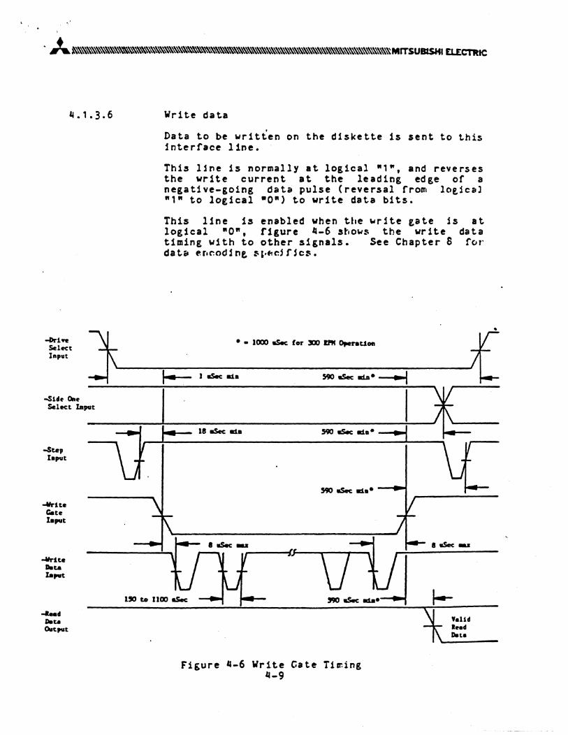
Data to be written on the diskette is sent to this interface line.
This line is normally at logical ft,_, and reverses the write current at the leading edge of a negative-going data pulse (reversal from lOticaJ .'ft to logical ·0·) to write data bits.
This line is enabled when the write gate 1s at logical ·0·, figure ~-6 shows the write data timing with to other signals. See Chapter S for date. er,C':odine. sl,(o!c:.1fjcs.
• • 1000 .sec for 300 UtI OperaU ... -Dri" J
Input ______ ~----------------------------------------~---------I... J.sec ilia 590 .sec IliA· ., I
-Step Iaput
-write c:.te Iaput
-write Data x.put
--~------~----------------~--------------~~
L liS IISec lit.
590 IISec me a ---"'" ,.. _____ ....;. ____ _
, ,
Figure 4-6 Write Cate Ti~ing 4-9
~ •• U' lead Dou

In use
An LED indicator on the front panel lights when this interrace line goes to logical ·0·. The LED can also be lit by drive select. See Section 7.0 for related options.
Motor on
This interrace lS~e starts the spindle motor when it goes to 10&ical ·0·. See Chapter 7 for related options.
The motor-on line loes ~ogical .,. to stop the motor and keep it off while the drive is out of operation, thus reducing system he~t generation.
Low Write Current, Low Speed, Head Load
This input has three possible uses. depending on whict. option"s are se.1ected on the main PCB. See Chapter 7 for the specific option settings.
Low Write Current:
This interface l~put i~ 8 l~tSc~) ·1· for high density disk operations. It is changed to 8 logical ·0· ADlx when wrJtio& on a low capacity dIsk. This. is necessary to i~~urf! reliable read/write operation. The state of this input ~~t be ~eld constant for 8 minimum of 590 uSec arter the Write Gate input goes to 8 logical·'·, (high) level.
Low Speed:
Bringing this i~~ut to a -low· state causes the spindle motor to slow to 300 RPM. A transrer rate of 250 (bit/sec must be used in this mode, along with narmal density media. The write current is also lowered by this selection.
Head Load:
It 1s possible t~ u~e p1~ 2 as a head load control input, but only if it is used exclusively in the 1.6 .egabyte .od~. See Chapter 7 for complete details.
11-10
'. ,

. ' "
~.'.ll
4.1.".1
\: " \ '" ,\ , '" \\,\ .. ,'\ \\\ \
Output sl,nal lines
The "_8S~-'S has rive standard output slEn~j lines. All pr them are multiplexed by the drive select lines. U~t1l the un1t 1s enabled by Its dr1ve select 1nput, all of the outputs are In the ·orr· state.
Index
Th1s sends t111e
interrace l'ne 1s normally lo,ical ., ft but • los1cal ·0· output pulse 3 liS wide each
the diskette .akes one revolut10n.
Th1s s1&nal &1,n,r1es the start or a track on the rotatins diskette. The index s1&nal t1mlne 1s shown 1n Fl1ure '-7.
3.0.s.e ~ ~~ _____________________ 1'7.s.e· ____________________ ~~
~
Fl,ure 4-7 Index Output Timin,
,-''

&1.1.".3
- Q~ret:tl0n· Input
- sup Input.
- Track 00 .,)U t. put.
Track 00
When this interface lS~e is at logical ·Oft, 1t indicates t~8t a r~ad/write heed of the selected drive is positioned on track 00. It the output of the selected drive is at logical ·1·, 1t indicates that the read/write head is positioned on a track other than track 00. See F1gure 11-8 tor tim1ng details.
lead data
This interrace l1ne transmits the data that 1s detected by the read/write head on the diskette.
The read data line is nor .. ll, logical ·1" but 1t . sends a logical ·0· (netat1ve-eoint) output pulse during a read operation. Refer to Chapters 7 and 8 tor timing detalls.
Stepp1n; Outward ""s .... , .. 1 .....
1.0 ..sec .... - ........ 1 uSee Ma& - __ lit
F1gure 11-8 Track 00 T1ming 11-12
... ,:,"

Ready/Disk Change
This interface Une 1s lo£icil) "'" when the dClor is open or no dis~ette is in the drive. The line goes logical "0" (ready) if an index pulse is detected twice or more, DC power (+5 V and +12 V) 1s within limits, and a diskette i~ inserted into the drive and the door is closed. See Chapter 7 for related options, and figure ~-9 for timing dptails.
A "disk chan£e" feature 1s also available on this output. This is used when knowled£e of a disk ChCtf't,e i~ the dr i ve is necessa ry fCit M.ft.\oo& rp rE-Ct~C:f1f;.
~.1.~.5 Write protect·
~tor On (Pf1) -Driwr ~l (ItS)
Input. (option)
-Jndu Output
~.d,.
Output
This 1nterface s1tnal notifies the host system of the insertion of 8 diskette without a write enable notch into the drive. The Signal eoe~ t.o logical ·0" when a write-protected d1s~ette if; in~erted into the drive. When the siena1 1s at logical "0", writing on the diskette" 1~ int,ibited even if the write eate line becomes actJV~.
.... J---- 600 .sec ....
Fieure ~-9 Basic Ready Timing "-13
l¥SecKu-....

~.2 POWER INTERFACE
Zl.2.1
DC Yoltaee
.5 V DC
.'2 V DC
The M~B5~-1S requires two types of DC power supplie~.
One 15 .12 V DC, which drives the spindle motor to rotate the diskette. It is also supplied to the stepping ~otor and the read/write circuit. The other 15 +5 V DC, which is used for the lo&ic circuits and the read/write circuit.
DC Power
DC power is supplied via connector J2/P2 on the bac~ of the printe~-clrcuit board. The spec1ficatior:s of thE' two DC voltages are shown in Table q-3. The pin arrangeme~t of co~~ector J2/P2 is shown 1n Table q-1.
Voltage Current Maximum ripple voltate varlation (peak-to-peak)
%0.25 V 0.7 A maximum 50 mV
(:.51) 0.5 A typical (seeking)
%0.6 V 1. 00 A max i mUir, 100 mV
(:51) 0.5 A typical (seeking>
Table 4-3 DC Power Specifications

5. PHYSJCAl INTERFACE
Electronic interfaces bet~een the ~~e5~-'S and the host syste~ are accolq,11shed with thrf'e connector~. Connector J1·is for U:e ~ignal j~terface~~ co~nector J2 for the DC power supplies, and connector .is fCJt fr·ar.ie trOundir.(;.. ;II~ co~nectors used for the H!le5~-'S and r ecoDinlended matin£ cc.nnectors are descr lbed below.
5.1 SIGNAL CONNECTOR
.400 :.0 (10.16 :0.
10
J1 1s a card-edge type, 3~-pln (for both pins for a single side) connector with pins (2,~. to 34) on the parts side and pins (1,3, to 33) on the soldered side.
sides, or 17 even-nulI"lbered
odd-nulI"lbered
A key slot 115 provided between pins" and 6 for the polarity reversal prevention.
The dimensions of J, are shown in Fig. 5-1.
Recommended P1 CD~nectors that ~ate with J1 are shown 1n Tables 5-1 and 5-2.
--!t-- . -'
I (0.91 :0.010) 2 -- T 34 . .
o 36 • 004
450 :.010 25) (11.43 :0.25) I I
• , --{ t-- .050 NOH ~
~ I' U.27) t--.OSO NOM .100 NOM
(1.27) (2.54)
8OAlU> '1'81 CCNESS 0.62 :0.007 <1.6 :0.1)
1.075 :0.10 (S.OB :0.25)
•
--1 L-. .063 NOM (2X) I (1.60)
·1
Fig. 5-1 Connector J1 Di~ens10ns (mm) and Pin Nu~her~ S-'
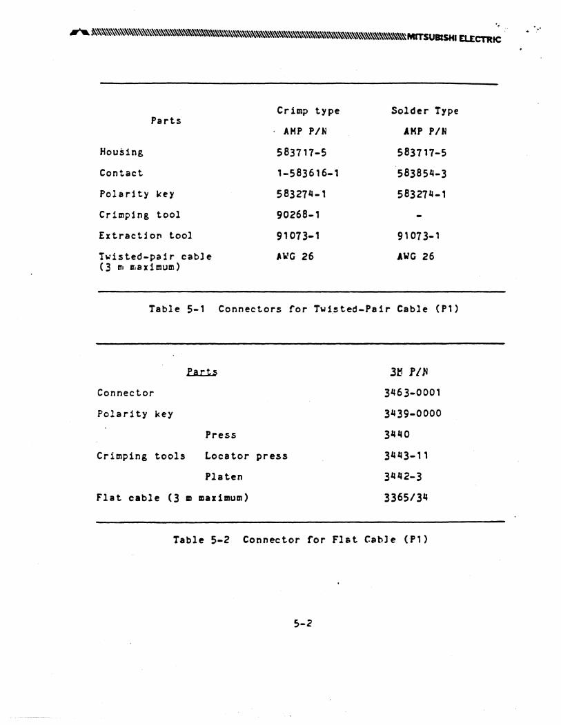
Parts
Housing
Contact
Polarity key
Crimping tool
Extract1oT' tool
Twisted-pair cable (:3 ITI Ir.S X 1 mum)
Crimp type
AMP PIN
583717-5
1-583616-1
583274- 1
90268-1
91073-1
A.'G 26
Solder Type
AMP PIN
583717-5
583854-3
583274-'
91073 .. ,
AWG 26
Table 5-1 Connectors for Twlsted-Pa1r Cable (P1)
Parts 3H p,~
Connector 3463-0001
Polarity key 3439-0000
Press 34lfO
Crimping tools Locator press 3443-'1
Platen 34!12-3
Flat cable (3 III lIIaximum) 3365/3!1
Table 5-2 Connector for Flat Cable (P1)
5-2

5.2 DC POWER CON~ECTOF (J2/P2)
J2 1s a four-pin DC power connector ~ade by 1 DCc-ted on the back of the pr inted-c~ rcuS t boa rd. ~ on connector J2 1~ located closest to Jl/P1; arran£ement of the pins ~~ viewed from the side :.hc:"'r, in F1E;\,;re 5-2. Pin numbers are shown on the ::.jc\f>.
M~Pt Pin the is
parts
Ttaf> C"cl'lnector~ on the drive side and cable side are shown in Table 5-3.
P2 (Cable Side) J2 (Drive Side) Parts
AMP PIN AMP PIN
Housing 1-1180424-0 172349-1
Contact (ti pins) 60619-1
Crimp tool 90124-2
Ext rae t:l Cl r, lool 1-305183-2
Cable (3 It max.) AWG 18
Table 5-3 DC Power Connectors
Figure 5-2 Connector J2
5-3

5.3 fRAME GROUND CONNECTO~ (J5/P5)
FA SlOtt 1 erllljCl~l
AMP P/I~ 6C920-1
~rJ,"p :r~rJljnlll
AMP PIN 60972-1
';r I, ~ . . "

"
5.~ INTERFACE CONNECTO~ P~YSlCAl lOC~TIO~
Figure 5-3 shows the physical locatlons of the interfac~ COPH·ctor~ used for the ~qe51j-'~.
P2 AMP PIN 172349-1
J2 ~ PIN 1-480424-0
AMP PIN 60920-1 AMP P/ri 6097f~~
~/ DRIVE PCB
31 CONNECTOR SCOTCH FLEX . PIN 3365/34, OR AMP PIN 583717-5
Figure 5-3 Connector Locet1on Diagram (Rear View) 5-5

5-6

· .. '"
6. PHYSICAL SPECIFICATIONS
6.1 !~STALLATIO~ tlRECTIO~ . The H~8S~-1S disk drive shown in Fig. 6-1.
Slant mounting perpendiculer.
should be within 10 detree~
(PCA UPPER)
LED -(Door open to left) (Door open to ri9ht ) (Door open to upward)
Fig. 6-' Disk Drive Installation Directions
6.2 DIHENSIO~S OF H~S5~-1S
See Fig. 6-2
6-1

- - ......•.........•.•.•.•.•.•. - •••.•••• ,,--.... ""--,,~""'''~'''''''\~\\\\\\\\\\\\\\\\\\\\\\\\\\\\\\\\\\\\\\\\\\\\\\\\\\\\\\\\\\\\'\ MlTSUBlSHI EL£CTlfI~
MOUHTINC Dc:Connec:tor aolderin9 .side
-f§ /'~'." ?:~: !'" .... '" ~ ~ ,+ • ~ - .... 4-1-#--. - -. 1 __ -1_ 1+ .+ ,. ? ~ • c tl
'"" • 0 0 "" lor' "" - .
14HAX
Note: All dimensions are in am diMensions in ( ) are in inches
• ON 80TT0H ,6-32.2SDP 2 ON EACH SIDE '6-32.2SDP
Figure 6-2
6
195 :t 1
Dimensions or M48SQ-1S 6-2
n o :3 :3 It n &
PCB .,

, .'
7. USER OPTIONS
Hon-standard modes of operation are available to the customer by using option plugs, and some PCB cut and/or Jumpers. When using a plug, installing the opt10n plug on a pair of aqulre pins is a ·short" condition, and re~oving it is an ·open·. 'trac~ or a soldered w!re jumper between two pads 1s a ·short·, and none 1s 8
·open".
If necessary, these plug-on Jumpers may be purchased fro~ ELCO, with a part number of 00-8261-0282-00-878.
Th~ sp~cific optIons are explained below.
7.1
7.1.1
DRIVE SELECT OPTIO~S
OSO TO OS3
When two or more rODs are connected·to the system, Jumper one of the four choices to allow the drive to be enabled when the particular select line is taken to a logical 80· condItion.
Only one drive per s1ste~ may be dea1gnated for each dr1ve number. In other words, there can only be one dr1ve ·0", etc. in a syste~.
7. , .2 HI
If only one roo 1s in a system, thIs option may be used to constantly select the drive. It causes the drive to ignore the status of the 80S" lines.
This Jumper must be removed 1n mult1-dr1ve systems.
7.1.3 TO
This option allows the user to have the ~ OS line (OSO, DS1, DS2, DS3) used on .ore than one drive. Specifically, it discoDnects the discrete terminating vesistor that is connected to the DS I~ruts. This would Anlx be used for special test situatIons.
7-1

7.2 KOTOR COJTaOL OPTIONS
7.2. ,
7.2.2
7.2.-
Various vays or turning on the spindle motor are avallable to the user. The controller deslgn and the tlming requirements or the total .,stem must be considered for'this.
teotor On Input
HH = Short KS = Open
This combination viII cause the spindle aotor to rotate 1f a 10g1cal ·Oft is present at the ~tor on 1nput, and a disk 1s 1nstalled 1n the drive.
Drive Select Input
MH = Open MS = Short
This combiaat10n viII cause the .piadle aotor to rotate If ODe of the drive select lnputs loes to a logical ·0·, and a disk Is Installed In the drive.
Motor On or Drlve Select Inputs
MH = Open HS = Open
Thls combination wjll cause the spindle motor to rotate 1f either the motor on or a drive select input Boes to a logical ·0· level, and a disk ls installed 1n the dr1Ye.
In-Use Latcbed Input
KH = Short MS = Short IU = Short
This combination viII cause It the In-use lnput and the that the la-use condition lnstalled In the drive. details.
7-2
the spindle motor to rotate. drive select Input are such 1s latched, and a disk 1s See Fl1ure 7-1 for t1~ine

" ',""" '" '
7.2.5
7.2.6
Dual Speed Operation
SS = Short sa : Open
This combination allows the drive to be used in a dual speed ~ode. Normally, the drive will be 1n 360 RPM, 50C Kbit/sec, ~ode. If pin 2 of P1/J1 is a.de -low", the drive changes to 300 RPM, 250 [bit/second operation.
Single Speed Operation
SS = Open sa = Short
This combination will cause the tloppy disk to always rotate at 360 RPM. The transfer rate is 500 [bit/sec tor 1.6 Mbrte and 300 [bit/sec tor 1.0 and 0.5 Mbyte capacity. The -Low Write Current- input .ust be taken wlow· to correctly record on a normal density floppy diskette.
7-3

-In \ / U.e
Input ~ _________ ~
- Drive 5elec::t Input
I-In U.e LEO)
I-Motor On)
---J/
Fleure 7-1 In-Us. Latcb Tlalnl
(/~--------------------~r~
S
1 s ,
f ~ ________ ~ ________ ~·~r __ ~~ __
{
.... Nrtte -~-------------\ Openu_
I
Fi1ure 1-2 Current leadJ (I) Tlaln, 1--

"
7.3 READY/DISK CHARCE OUTPUT OPTIONS
7.3.1
Depending on the controller design and the system timing require~ents different ready output options may be selected.
Current Ready (I) Option
25 = Open PC = Open
This combination will have the drive ready. output follow the rotation of the disk. If the disk is not rotating the output will be a logical -,-. If the disk is rotating and two index pulses have been sensed 1n the correct .~ount of t1ae the output w1ll be a logical -0". See Figure 7-2 for timing details.
Held Ready (II) Option
2S = Short DC = Open
This cOlDbination a logical -0" sequence and from the drive.
will have the drive ready output go to state during the dynamic clamping
stay at -0· until the disk 1s ejected See F1gure 7-3 for timing detail~.
Disk Change Option (Drive Select Reset)
2S = Short DC = Short
This cOlDblnation will cause the drive ready output to be a logical -,- whenever a disk is properly 1nstalled in the drive. (Hote that the polarity of this 1s reversed from the previous options) 1s seen in Figure 7--, this option is best used with. system controller that -polls- the disk drives 'for their status. Tnls iEo bec~use 1t is not the insertion of the disk that resets the -disk change- flip-flop, but the -low· to Whigh· transition of the drive select input. This means that .fter • disk is installed 1n the dr1ve the correct status vill be outputted on the second pulse.
7-5

(Di_ la) (launal)
~------------~{f~----------------------~r~
T> XIO .s.c t 1'----~--~ S~--------
(Pi.1t In)
(PUk' Chan.;el
- Drive Select. Input.
- a •• ely Out.put
~ ______________________ ~~r __ ~ ____ _
f
Fi,ure 7-3 Held lead1 (II) Tilling
1 Dtak Out
'4
/ Disk In
1 USee MA. ..._ 1 USee MAx
Fl,ure 7-- Di'ak Chance CDrlye Select leset) Tilling 7-6

(-Disk Chenge)
-Step Illput
.aead, Output
Disk Change Option (Step Pulse Reset)
2S = Open PC = Short
This option 1s the same as the preceedlng one, except that the -high· to -low· transition of the stepping input resets the drive status.
Radial Ready
RR = Open
This option viII cause the ready output to always be enables; the" drive sel ect1nput viII bave no effect on the ready output. The logic of the ready output (2S, DC options) is ~ .ffected by IR.
Disk O"t Disk III
F1&ure 7-5 Disk Chan&e (Step Reset> Tl.lng 7-7

HE~D LO~D OPTIONS .
Hany alternatives are available to the user on how to cause the read/write head to load onto the disk. To prolong disk life, the head should be unloaded as ~uch 8S possible. Also, increased throughput can be reali%ed by keeping the spindle ~otor tur~ing,and then loading the head whenever disk access is required, because head loading is much Quicker thin starting the motor. But, this may not be a factor if sin£le, lont accesses are preformed.
7.11.1 Head Loading with Drive Select
HS = Short
- Motor On
- In Use
Instal11ng this plug w11l cause the head to load when tbe drive is &elected by DSO through DS3. This occurs only if a disk 1s installed 1n the drive w1th the door closed. See rigure 7-5 ror a schematic of this and other head load options.
~ote: As seen 1n Figure 7-6, used at the same time, but HH same ti~e as the option 1t is option DH.
---0 MSo----,
---0 HMo------. ----OMlc--1----~~--~
-0 14M c----.::::~
HS, 8M, and HL can be DJst no·t be used at the
connected to through
• Head lOld Drher
• ~ld Reidy
(Pull-up Reststors n.ttted For Cllrtty)
Figure 7-6 Head Load and Spare Input Options Sche~at1c 7-8

· , ,
7."."
7 • .11.5
7.".6
Constant Head Loading
He : Short
This option will cause the head to always be loaded after the door ~s closed on a disk.
Head Loading with Motor On
HM = Short
This option will cause the head to load if the motor on input goes -lowR, and the door is closed on a disk.
Head Loading with In Use
HL = Short
This option will cause the head to load if the in-use 1nput goes -low R, and the door 1s closed on a disk.
Head Loading with Spare
HH = Short SP = Short
This option will cause the bead to load if the spare input goes -low R, and the door is closed on a disk. DH ~ay be used to qualify this action with the Drive Select inputs. The HH option cannot be used if pin 2 on P1/J1 (Low Speed, Low Write Current is being utilized.
Head Unload Delay
UD = Open
In order to eliminate unwanted oscillation of the head load solenoid, a delay may be introduced after whatever head load aignal being used 15 .ade -raIseR. This delay 15 ~ lndez pulses, which equals a ti~e delay' of 600 to 800 .Sec.
7-9

7.5 LEO OPTIONS
7.5.1
7.5.2
7 .• 5.4
A front panel LED (also called the ·In-Use" LEO) 1s provided in the "4854-1S. Its purpose in most cases is to alert the u~er that the drive is being used, and that the disk should not be removed. It can also act as an indicator of progra~ execution status. Many different modes of operation are available, which are detailed below.
In-Use Input or Drive Select
IU = Short
This combination will cause the LED to be on if either the In-Use or drive select inputs are made active.
Drive Select
IU, = Open
This combination will cause the LED to light only if the drive is selected.
In-Use
IU = Short IS = Short
This combination will li£~t the LED when the In-Use input 1s input is active.
In-Use Latched By Drive Select
IU = Short IS = Short IL = Short
This combination latches the state of the In-Use input on the -high· to -low· transition of the drive select input. See figure 7-1 for timing details.
7-10

..
7.5.5
7.5.6
Head Load
IS = Cut PCB Trace = Short Open Pads .
This co~binationcauses the LED to light whenever the read/write head is loaded. It totally ignores all InUse circuitry and other jumpers.
Ready Qualifier
IF = Short
Shorting IR the ready used). If of lighting the door 1s
causes the In-Use LED to be qualified by atatus (D1sk Change options cannot be used with -held read,· th1s has the effect
the LED only if a disk 1s 1n the drive and closed.
1-11

7.6 INPUT TERMINATIONS
7.7 .
All Input lines to the drive are terminated (see section -.1.1). The resistor pack should be removed on drives 1n multi-drive systems, wjth the exception of the drl ve the farthest electrical distance from the system controll~r.
FRAME GROOND
Normally the frame of the drive Is connected to the logic ground through a resistor-capacitor network. If this Is not desired it can be disconnected by cutting the FG trace. See Figure 7-7.
HOST SYSTEM DISK DRIVE
+S V .~
GND .. GND .~ ..
100 K Om"
+12 V ." FG
~.-~
FRAME GROUND .... _- -t]---- 1. __ ......
.
Figure 7-7 Frame Ground Circuit 7-12 •
~
~
1.h E _.01
- uF
4.

, , . ""
7.8 OPTIONS SUMMARY (Table 7-0
Name Description Type Factory Shipment
Open Stlor t
DSO Drive Select - 0 Plug X DS1 " " - 1 " X DSZ " " - 2 " X DS3 " " - 3 " X HX " " - Continuous " X TD " " - Termination " X
HS Head load - Drive Select Plug X HC " " - Constant " X HM " " - Motor On " X HL " It - In Use " X HH " " - Spare " X UD II, " Unload Delay " X
SP Spare Input - Enable Trace X DH (HM) " " - HM Route " X DH (HL) " " - HL Route " X
IU In Use - In Use Input Plug X IS " " - No Drive Select " X IL " " - latched " X IR " " - Ready Qualified " X IH-1 " " - Normal " X IR-Z " " - Head load " X
2S Ready - Held Ready Plug X DC " - Disk Change " X RR " - Radial Output " X
MH Motor On - Motor On Plug X MS " " - Drive Select " X SS Motor Speed - Dual Speed " X SB " " - Single Speed " X
FG Frame Grounding Trace X
Table 7-1 Option Summary
7-13

r--------------t , • ';".-:::V'. ~ , .... J : ~ ... .:. g': ,,-- --",.. - . '''' U I = 2 3
·s 0
... ~ .. :-
F ..
-Ie ••
r..
o
I ••
••
. . I • • r--·-- ..... ----; '''' t.. ___ •• .. _~ 110
JI: .. -· · ·
o ] 0
I i -. I 1111----- :
.. ~ ----, r. r'"l .. t -.::;- 0 ~ •
F
G o
H
l±IL - J I:
D.
figure 7-8 PCB Option Locations 7-14
,-.. .

_ . ." .
8. RECORDINC FORMAT
Data to be recorded on the floppy disk is grouped in various blocks.
There are bits, bytes, sectors, tracks, and sides. The bits are encoded onto the disk by three possible means: FM, MFM, or r.r.FH techniques. These bits are collected together in a certain number of bytes per sector to define the actual recording format used. All of this is defined by the host system; the disk drive just records and detects flul reversals on the disk.
-8.1 BIT ENCODING.
As stated before, there are three main encoding bits on a floppy disk. All advantages and disadvantages,. but the accepted standard is HFM (also called Double
lIethods of have SorliE!
generally Densi ty).

4/rit~ Detll Input
8. , . ,
-lead Data Output
FM £ncodine
F~ (Frequency Kodulatjon) encodIng is shown in Figure 8-1. It 1~ the simplest ror~ or encoding. and may be decoded by use of inexpensive one-shot mult1vlbrators. It can do this because each data pulse is between two clock pulses, thereby defining the wread window" very precisely. Values shown are for a 500 Kblt/second transrer rate. ~ultlply all values by 1.666 for 2 300 kblt/second transfer rate, and by 2 for a 250 Kbit/second transfer rate.
Clock
Clock
Dau (0)
ISO to 1100 ~e
Clock nau (1)
Figure 8-1 FH Write Tl~lng
nata (0)
200 aSec aso
nata 0)
nata (0)
2.00 uSee t 10 .see 4.00 uSee t 20 .see
Data (0)
2.00 uSee t 400 .sec
Iote: Spindle Spee4 Variationa Eaeluded 4.00 uSK t eoo .sec
Figure 8-2 FH Read Timing 8-2

. , ", ......
8.1.2
C D D
CE1.1. 0
111
u u 20Dnsec~~ ~ .. an
2.00uSec
I e f
C D D
CELL 0 CE1.1. 1
UI UI
u U
':'=1t ~ 2.00uSee -400,,5ee
HFH Encoding
HFM (Modified frequency Modulation) encoding records twice the numper of bits per inch (linear recording density) as FH encoding. but has the same number of flux changes per inch. It does this by removine the clock pulses, and shrinking the bit cell space by 50S. See Figure 8-3 and 8-4 for specific details. Clock bits are always written at the leading edge of the cell only if no data bits are written 1n either the present or preceedlng bit cells. Values shown are for a 500 Kbit/second transfer rate. Multiply all values by 1.666 for a 300 kbit/second transfer rate, and 2 for a 250 Kbit/second transfer rate.
l eD ,eD
CE1.1. 2 CELL 3
JeD leD
CELl. 4 CE1.1. S
III COl Cli (01
u u· u .
~ •• OO u5e&:--_" ~3'00 usec~
figure 8-3 MF~ Write T1~ing
I C D
.1 C D I c D I c D I C
CE1.1. , CELL 2 CELL ) CELL 4 CELL S
UI (01 (U (01 (01
U U U
h C.OO uSee 0.' uSee
, I, .3:00 us.e~ -0.' uSee
figure 8-4 KFK Read Timing
B-3
IC DIC DI CELL '7 CELL.
(01 III
u u
D
I C D I C
D
CE1.1. ., CE1.1. •
(01 III
U u-

8.'.3 HHFM Encoding
MHFH (Modified-Hodified Frequency Modulation) is al~o a wdouble densityft encoding method, but it further reduees the number of-eloek bits used to fill the empty spaces between dsta pul~es.
It is not a standard encoding technique, and should probably be avoided for that reason. See Figure 8-5 and 8-6 for a description of MHFM. The data bits are written in the middle of the data cells, but a clock pulse is encoded only if no clock or data pulses were written in the previous bit cell, and no data bit is to be written 1n the present one. Values shown are for a 500 kbit/second transfer rate. Multiply all values by 1.666 for a 300 kb1t/second transfer rate, and by 2 for 8 250 Kb5 to/second transfer rate.
o 0' I C 0
CC~L 4 C£~L 5
ole ole °fC eE1.L 0 CCLL 1 CELL 2 CELL J
c e , e
CE1.L ,
o I COl CE1.L '7
COl III (11 III COl Cl) (0 I COl
u u 200nsee~~ ~ _In ~2.00~see~
1 uSee
C I 0
CELL 1 III
u u *2sonsec1~ ~
Z.OOuSec &400,,$ec
----------~u U~------------I~ U
L ----;>~I .... .:-J.oo usec+ 5.00 uSee 14.00 uSee po
Figure 8-5 HHFM Write Timing
C I D
CELL 2
(II
C I D
CELL 1
(0)
C I D
CE1.L 4
III
. C I 0
CELL S
CO)
C I e I 0
CELL '7
COl
·1
c I 0
CE1.L • III
u -----------,u~-------~u~------------~~
I.. 4.00 usec: ___ -tl{~"'"":· l.OO usec:-+- 5.00 u$ec ___ --j~~ ~!O.' uSec: *0;6 uSec: *1.0 uSeC:
Figure 8-6 HHFM Read Timing 8-4

' .. ' .. l' ,,' "f
•
8.2 H4854-15 RECOMMENDED FORMATTING5
H4854-1S 51/4·1nch Flexible Disk Drives use standa r~ Tur.nel Erase type Read/Write Heads, accuracy direct-drive brushless ~otor for rotation; guaranteed ~1.6S index interval Instantaneous speed.
Industry and h 19t.
spindle and ~2S
The recommended formattings for data i"terchange between drives are shown in the following figures, including for~att1ng and data re-write modes.
The dr1ve~ allow for the following conditions o~ all tracks.
(1) The leading edge of. data block should be preceded by the erased area when re-wrltten.
(~) The trailing edge of a data block should be covered by the erased area when re-written.
(3) The erased area should not overlap with Sector Identifiers.
(4) Read/Write gap should ~e before the next 1D mark as the erase curre"t is falling off When re-written with a fast rotation spindle on a slow formatted ~ector.
8-5

IMea Output
Ftrst Sector
I~ I ~;: r- .... ,ft. "I Sector Il\Clu Ident 1f1er C,p
ID Mar k
1£-(rr) 6-COO) l-{F!) •
I Address IdentHier
J- 00
ID Ftrst D.t. "ock Data '.p ~DC
Ilock Dltl I Dati 'IP te ... k Fteld
11.(Fr) 5-(00) lZ1 lyles z·e) 27.(FF) I-(FI)·
' ....
L Sector --- 16th l ~ I ) ~
Track I '.p
101 "0-1".1 C,l. S'ele Sector
1.{DOI I .. 00 1-(00) Z-C )
eFr) u"tH Inde
• .tsstng clock tr.nsitio" bet.een bits C ."d 5
Figure B-7 1S0-7487/2 Style. Track 00. Side 0 (FM) 250 or 300 Ktjt/second Transfer Rate
U IMell Output
llIdu &ap
lZ-(CEl
F'rst Sector Count I St.rt r- ------I ae-Vrite .. I
Sector ~ 1--- 16th l ~-"'---I Track
Clp Sector 10 First D.t. Ilock Data \ Td,ntHhr c.p "oct
ID I Address O.t. I Dlt. I EDC 'IP \ Mark Identif'.r .... k F.eld
12-(00) Cyl I-C ) 22·(U) 12.(00) 256 .ytes Z·( ) 50-(4£) l-CAl ). S'de 1-(00) '.(Al)· to I-eft) or (01) I-(FI) 54-(eE) ~a--ended
Sector 1-1 ) 1- 01) EDC t-e ) • .'sst"g cloct tr."sltton bet ... " btts 4 .nd 5
Figure 8-8 1S0-7~87/2 Style. Al~ Other Tracks (HFM) 250 or 300 Kbit/second Transfer Rate
8-6
330 no-1n,l to
266 no-1nl1 (CE) unt 1\

· . ~. ,
Iftdea Output L First SKtor
~ 1--- tth l SKtor
~~I~ Trick '-p
111dea s.ctor 10 First Deu "otk Deta \ '-p Jd!lIt 1 ff.r '-p "ock ID )Addren Dlta J Detl JEDC c.p \ Mark Identff1er Mart Fte1d
32-(4E) 12-{OO) C,t. I-I I Zz-(eE} 3- Al)· Sfde I-I- Ft) S.ctor'l- .
1- OZ [DC Z-
IZ-foo) 51Z Iytes s- 11)· 1- n)
2-( } 17-(4[) to
1O-(4E) rec~ellded
4C' nalna' to
ZCZ no.lna' (CE) until JndeK
Jrldea CAp
Sector ldeilliner
Figure 8-9 512 Bytes/Sector, Standard Format 250 or 30C Y.bjt/second Transfer Rate
IMea Output
First Sector "r-- Sth l s.ctor
I Il - "-Write ~ I
Surt
ColI t
fD FIrst Dlta Ilock D.tl \ Cap ~ I Ilock 10 I Adc!re" DIu J DI~~ ~Dt c.p \ Mark '''.Ufter Mart FIeld
293 no.tnal to
Z43 ft~fnal
I :=/1 fZ-C 4E)
I. 03 z-
(CE) untl' Iftdel EDC • Miss.". clock traftsttloft bet-.-n .Its C .nd 5
Figure 8-10 1,024 Bytes/Sector, Standard format 250 or 300 Kbit/second Transfer Rate
8-7
Dltl ~.ctor
110ck Identtffer 'ap ID J Address
,.."t Id,"Ufter
Inde. OIIt",t
Ftrst Sector Coullt
Start r- -I Ie-Vrft. .. I
10 First Dati .'ock Cap
Det. I Data ~DC Kart ,t.ld
Sector ~I··-l't" l Dati \ .'oct Cap
\ ~ I TriCk Cap
..
L
I 54-(4E) 1'-{ J Cy1.
J- AI • Std. 1- Ft Sector
lSI Ittls 2.( ) 54-(eE)
EDC • Mflsf .. cloct trallsftfon .. t.ee •• tts e •• d ,
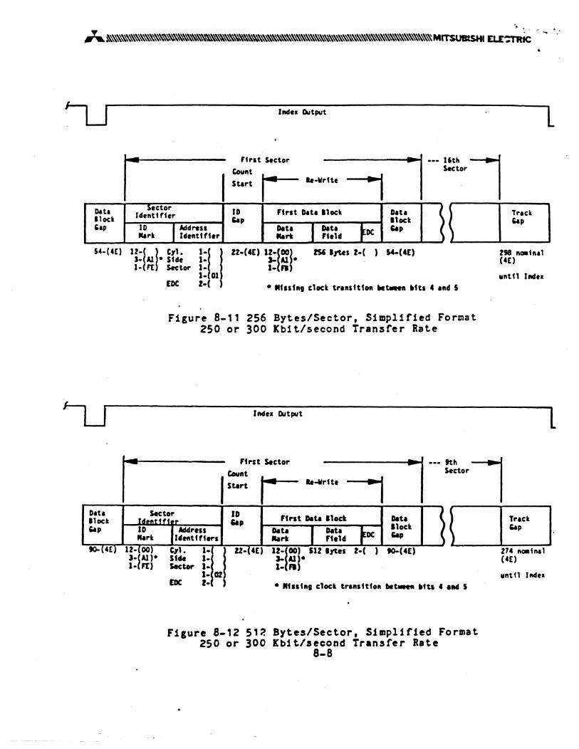
Figure 8-11 256 Bytes/Sector, Simplified Format 250 or 300 Kbit/second Transfer Rate
Indt. OIIt",t
unttl Ind ••
l
I ~ I S~lIrt':rst SectDr ~ 1--- ::tDr l .. r- le-41rtt. "I
~E-~-\-~--Sec-to-r-~-r-.-ss-+-~-P-~-De-:-~-t-Da-tl-·-'-~---DC~~t-'p:-:-t~~l I~ I. IdetlU tt.rs ) _ _
Cll. 1. I u- 4E) to-(4E) 27e noatnll Stde I· (eE) Sector I-
I- 02 untfl Ind •• EDt!- • MfIIC" c'oct trallsfttoft .. t.ten .fts c .Id 5
Figure 8-12 512 Bytes/Sector, Simplified Format 250 or 300 Kbit/second Transfer Rate
8-8

.... . ~'
Indu "P
U6-(4E)
IlMIea Output L rtr,t Sector
Count I Start r- .. -Wrtt. "I Sector "1--- 16th l ~-I"'--~:" I Sector SD Ftrst Dat. 110cl Dlta \ Id.ntt ft.r '-II 11oc ..
10 J Addreu Dat. 1 OIta I £DC '-P Mark Identtfter ICoar" neld )
12-~OO) C". 1.( 3- Al)· Std. 1.( 1- F[) Sector 1-(
S.L. EDC· 2-(
I Z2-(eE) 12-{OO) rs, lyle, 3- Al)· 1- FI)
2-( ) 50-(4£) to
54.(4£)
Figure 8-13 256 Bytes/Se~tor. NEC,765A Format 250 or 300 Kbit/second Transfer Rate
21' ~tn.l to
152 ~tn.' (eE) until lIMIt
u' IlMIu Output L Ffr,t Sector
I':~ r-IlIdu Sector ID Ffrlt Dlt. 110ck Dlt. \ ;'p IdenU,ter '-II Ilock
ID ICoark
146-( 4£) U-fOO) . 3- Al)·
I· F[)
'AIUreu IcSenU 'fer
C,1• Sf4e Sector S.L. EDC
Data 1 ~!~d Mlrk
r2-(C~) 12-fOO) 512 lyle, 3- Al)· 1- FI)
JEOC Z.( ) 5'-(4£)
to
\
7'-( eE) r.c_IMIed
Figure 8-1q 512 Bytes/Sectord NEe 765A Format 250 or 300 Kb1t/second Transfer Rate
8-9
Tr.ck "P
335 ~tn.l to
25e ~fnll
I (eE) unttl IIMI ••

htdea '-p
'ndea OIItpul L 'frst Sectbr
I!:":: r- .... ".. -I "1--· 5th l Sector
~ I ~:'. 'I Mctor 10 Dati
~ Identifier ;.p 11 oct 10 ,AddreSS Data 1 D.t. ,[oe ;'p \ ",,.It Id.ntt fter "'rt Ffeld
12·(00) Cyl. 1.( I 12-(eE) S.(Al)· Stde 1-(
Sector I-l S.L. I- 03 . tDC I-
1'-100) 1.024 lyles 1-( ) 10-(4£) ~Al)· to I. n) 101.(eE) rec_nded
• Mf,st., clock .tr.",ft(o" btt ... n btts e .ad 5
Figure 8-15 1,02Q Bytes/Sector, BEe 765 A Format . 250 or 300 Kb1 t/second Transfer Rat.e
Figure 8-16 512 Bytes/sector, 1S Sectors/track 500 (bit/second Transfer Rat.e
8-10
12e "c.f".l to
169 ftc.i".l (4[) u"til Index

.' /pI
"
lMu Ca,
lMea Ca,
.:H:4E) U-(OO) . Ha)-_-(PC)
»-(4£)
s.ctor f'L1"ft lata IIlDCk lata \ r"'t1u .. D IIlDCk
D f= Ga,
~ I~~ 1 IDe Ga,
\ tkrtt
Figure 8-17 1S0-7065/2 Style, Track 00 Side 0 (FH) 500 (bit/second Transfer Rate
I
L 26tb
lSe11 l kh s.ctor
~ I ~I letor Psnrt lata a.ct \ r ... uu .. lata D
1 J-: IIlDCk D I::=. c:., "ta lata Ga, ) ..... RaI'tI: 1'1.14 12~OO) 0,1. l~ ) H'l)- SUe I~OO) l~n) w (01)
SKtw I~ ) It. 1~01)
(02) (03)
IDe 2~ )
Z2~4E) lZ~OO) '-(iU-I-(n)
Z511re-512 Itue
1.024 arc-.
I~ )
5&-('E) e6-0{4E)
116-(4£)
• r.ctcw U • • •
1IM.e: Setor l-ctil SL .... " .. (Ol) ZS6 Ift- .ial, f. I:rId: GO ..... I.
tIItl_l .. cleek rz-ttl'--~ "ta 6 ... S
Figure 8-18 IS0-7065/2 Style, All Other Tracks (HFH) 500 rbl t/second Transfer Rate
8-11
F111 (4E)
,...(4£) 600-(4£) 6S4-(4£)

8.3
8.3. ,
~ ~" I ... '.
ERROR DETECTION AND CORRECTION
Write Errors
If an error occurs durins a write operation, It c.n be detected by perforll',lne a read operation on the diskette 1.medlately followlng the write operation. Thls 1s ,enerally called a write check, which ls an effect1ve means of preventing write err~rs. It is recommended. therefore, that a write check be ~ede w1thout fa11.
If a write error occurs, repeat the wrlte operatlon and conduct a wrlte check. If data cannot be correctl1 wrltten even after the write operatlon ls repe.ted about ten tlmes, pertorm a read operat10n on another track to determlne whether the data can be read correctly. If ao •• apeciflc track of the dlskette 1s defective. If data cannot be correctly read on the other track. the drlve ls .ssuaed to bave some trouble. If the dlskette ls defective. replace It.
Most data errors that occur are 80ft errors. If a read error occurs, repeat the read operatlon to recover the data.
The followinl are posslble maln causes of soft errors:
o Dust ls caueht between the read/write head and diskette causlng temporary fault 1n head contact. Such dust 1s ,enerally removed by the selfclean1nl wiper of the jacket, and the data is recovered by the next re-read operation. If read/write ls contlnued for a long time In a very dusty env1ronment, however. hard errors can result from a damaged diskette sur~ace.
o Random electrical nolse ran,ln, In time fro~ a rew .icroseconds to a fev milliseconds can also cause read errors. Splke nolse lener,ted by • switchins re&ulator. partlcularly one tbat ha. short swltch!n, Intervals, deterlorates the sttnal-toDolse ratio. and IDcreases the Dumber of re-read operatlons for data recover,. It 1s Decessary. therefore, to .ake an adequate check on the noise levels of the DC power supplies to the drive a~d fra"e ,roundlng.

, . p
· .. " A ~~~~~~~~~~~~~~~\~~~~~~~~~~~\~\~~\~~~\~~~~~~'\\'\\'\\'\\'\\'\\~'\\~'\\'\\'\\~~\~~'\\~~'\\\~~~MrTSU8tSHI £L.ECTRIC
c
o
Written data or diskette~ may have defect as cannot be detected by a during write operation.
so small a da tach ec I<
Fingerprints or other foreif~ ~atter on a written diskette can also cause 8 temporary error. If foreign matter is left on a written diskette for a long time, it can adhere to the diskette, possibly cau~1ng a hard error.
It is reco~mended that the following read operations be performed to correct these soft errors:
o St.er 1:
o Step 2:
~tep 3:
o Step l.I:
Repeat the read operation about ten times, or until the data is recovered.
If the data cannot be recovered by Step , move the head to another track, It·e o~posite direction of the previous track position before the desienated ~r~c~, and then return the head to the orlgln~) l,osjtlOfl.
Repeat an operatlon similar to Step 1.
If the data cannot be recovered, assume the error is a hard error.
8-13

8-111

t
J....*'''''''''''''''~~\~,,\~~''''\~,,~''''\~''''''\~,,~''''''''~\~''''~~\~''''''\~''''""\~"~MrTSUBlSHI ELEC'T1t1C
9.' RESHIPMENT PRECAUTIONS
When res~jpping the drive, proper step~ m~st be taken to prevent any damag~ to t~e drive.
9.1 SHIPPING DAMAGE
Ar.y damage to the drive that occured during shipping is the responsibility of the carrier. Contact the carrier for any damage claims.
9.2 RESHIPPING
If it is necessary to return 8 drive for any reason, proper steps must be taken to prevent damage to the drive.
o Use all the packing materials that were rec~ived with the drive, if possjbl~.
o Be sure to utilize the anti-static bae that came with the drive.
o The head protection sheet should be inserted into the drive (the door should ~ be closed).
Please refer to fj£ures 9-1, specific details of how to shipment.
9-1
9-2, pack
9-3, the
and 9-11 drives
for for

Bead protection sheet (Inserted)
Tape
Bead protection sheet (Before insertion)
StoPi>t!1"
NO'I'E: After inserting the head protection sheet, push the stopper in the arrow direction (a) until the sheet is securely in place.
Figure 9-1 Head Protection Sheet Installation 9-2

oJj -- " (",
,f
~ J... ~"""~"""~~~~~~~~,,~~~~,,~~~~~~~~~~,,\~~~\~~,,~\~~,,\~""~,,\~~\~""~~\~MrTSUBtSHI D..ECTRtC
Anti-st.atic bat;
'rape
Protective board
Place a ~esiccAnt in the bottom space.
Protective boar~
'rape from the front to the bott.om.
Figure 9-2 Bag and Board Assembly 9-3
FOO

,. ,
)..~\~"""~,,~,,_,,~\~~~,,~""~\'\~""""~~"""""""""""""""""""~\~"~MITSUBlSH1 ELE.··· '6 ".' .. ,
Thes. cushions ue t.M ...... 0 e1t.Mlr .f t.heta MY be ••• d at t.M top Olr bottca.
CUshion
Figure 9-3 Ten-Pack Carton Assembly 9-"

c.ah1011 (t.CIp)
!be C'WIh1on "a41.n9 -f'JIOHT OP-..t be at the top.
Qwlh1011 (IIot~)
'f'hII c:ualUOII r..c1a9 -rllOMT'-..t be 011 u.. IIott_.
Figure 9-~ Single-Pack Carton Assembly 9-5

•
.~
~.
A~"~~~~~~~~~~~-'~~~~'~"\~~"~~~~~"~~""\~'a~~M~SUBtsHa r:1;;~ ,,,~. "4 '
9-6