Embed Size (px)
Citation preview

1
SRI DHARMASTHALA MANJUNATHESHWARA COLLEGE
(AUTONOMOUS)UJIRE-574140
(Re-Accredited at ‘A’ Grade with CGPA 3.61 by NAAC)
Minor Research Project
On
DESIGN OF MICROSTRIP ANTENNA FOR
INTENSIVE INVESTIGATION OF HIGHER BANDWIDTH
Submitted to
University Grants Commission
South West Regional Office
Bangalore
By
S N KAKATHKAR
Principal Investigator
Department of Physics
SDM College Ujire-574240
May -2016

2
SRI DHARMASTHALA MANJUNATHESHWARA COLLEGE
(AUTONOMOUS)UJIRE-574140
(Re-Accredited at ‘A’ Grade with CGPA 3.61 by NAAC)
Minor Research Project
On
DESIGN OF MICROSTRIP ANTENNA FOR
INTENSIVE INVESTIGATION OF HIGHER BANDWIDTH
Submitted to
University Grants Commission
South West Regional Office
Bangalore
By
S N KAKATHKAR
Principal Investigator
Department of Physics
SDM College Ujire-574240
May -2016

3
CERTIFICATE
I hereby declare that the minor research project entitled “DESIGN OF
MICROSTRIP ANTENNA FOR INTENSIVE INVESTIGATION OF
HIGHER BANDWIDTH” has been carried out by me in the department of
Physics of our college granted by University Grants commission, New Delhi.
I further declare that the work contained in this report has not formed the
basis for the award of any degree of any university
Ujire S N Kakathkar
1-5-2016

4
ACKNOWLEDGEMENT
I am grateful to the management of our Institution SDME Society ,
particularly President of the Institution Dr D Veerendra Heggade,Vice
President ,Secretaries and Prof Mohannarayan K. S. Principal of the
Institution for all encouragement and timely support.
The University Grants Commission provided the crucial support that made
the project a reality. I acknowledge my indebtedness to the joint secretary and
Regional Head of UGC, Bangalore
I am grateful to Prof T N Keshav HOD of Physics and Dr Nandakumar Shetti
associate professor PG Physics SDMC Ujire for their guidance and support
I feel great pleasure in expressing my sincere thanks to all those who helped
directly and indirectly in completing this work.
S N Kakathkar

5
CONTENTS
Sl no Title Page no
1. Introduction 6
2. Objectives 8
3. Relevance of the study 9
4. Research design and methodology 11
5. Chapter - 1-antenna of circular shape 13
6. Chapter -2-Bandwidth enhancement-parasitic patches 16
7. Chapter 3-Bandwidth enhancement –additional lobes 21
8. Chapter- 4- Bandwidth enhancement –additional lobes 26
9. Observation s and Tabulations 29
10. Summary of findings 37
11. References 39

6
Introduction:
An antenna is a radiating element which is used to transmit and receive
electromagnetic waves.
Wireless communications has been developed widely and rapidly in the modern
world especially during the last two decades. The future development of the
personal communication devices will aim to provide image, speech and data
communications at any time, and anywhere around the world. This indicates that
the future communication terminal antennas must meet the requirements of multi-
band or wideband operations to sufficiently cover the possible operating bands.
However, the difficulty of antenna design increases when the number of operating
frequency bands increases within a single antenna.
The aim is to study and design various micro strip patch antennas of different
shapes for wireless communication systems and the investigation of higher
bandwidth
Microstrip Antenna
A microstrip antenna consists of conducting patch on a ground plane separated by
dielectric substrate. This concept was undeveloped until the revolution in
electronic circuit miniaturization and large-scale integration in 1970. After that
many authors have described the radiation from the ground plane by a dielectric
substrate for different configurations.
The first practical antenna was developed by Howe and Munson The early work
of Munson on micro strip antennas for use as a low profile flush mounted antennas
on rockets and missiles showed that this was a practical concept for use in many
antenna system problems. Various mathematical models were developed for this
antenna and its applications were extended to many other fields. A microstrip

7
antenna is characterized by its Length, Width, Input impedance, and Gain and
radiation patterns.
Various parameters of the microstrip antenna and its design considerations are to
be discussed.. The length of the antenna is nearly half wavelength in the dielectric;
it is a very critical parameter, which governs the resonant frequency of the antenna.
There are no hard and fast rules to find the width of the patch.
History
The rapid development of microstrip antenna technology began in the late 1970‟s.
The first aperture coupled microstrip antenna was fabricated and tested by a
graduate student, Allen Buck, on August 1, 1984, in the University of
Massachusetts Antenna Lab. This antenna used 0.062” Duroid substrates with a
circular coupling aperture, and operated at 2 GHz. As is the case with most original
antenna developments, the prototype element was designed without any rigorous
analysis or CAD - only an intuitive view of how the fields might possibly couple
through a small aperture. They were pleasantly surprised to find that this first
prototype worked almost perfectly – it was impedance matched, and the radiation
patterns were good. Most importantly, the required coupling aperture was small
enough so that the back radiation from the coupling aperture was much smaller
than the forward radiation level.
The geometry of the basic aperture coupled patch antenna is described. The
radiating microstrip patch element is etched on the top of the antenna substrate,
and the microstrip feed line is etched on the bottom of the feed substrate. The
thickness and dielectric constants of these two substrates may thus be chosen
independently to optimize the distinct electrical functions of radiation and
circuitry. Although the original prototype antenna used a circular coupling

8
aperture, it was quickly realized that the use of a rectangular slot would improve
the coupling, for a given aperture area, due to its increased magnetic polarizability.
Most aperture coupled microstrip antennas now use rectangular slots, or variations
thereof.
(iii.) Objectives:
. The aim of the project is to design and fabricate a Microstrip Antenna for the
intensive study of higher band width for various patterns.
(iv) Hypothesis:
Bandwidth is a fundamental antenna parameter. Bandwidth describes the range
of frequencies over which the antenna can properly radiate or receive energy., the
desired bandwidth is one of the determining parameters used to decide upon an
antenna. For instance, many antenna types have very narrow bandwidths and
cannot be used for wideband operation.
Bandwidth is typically quoted in terms of VSWR. For instance, an antenna may be
described as operating at 100-400 MHz with a VSWR<1.5. This statement implies
that the reflection coefficient is less than 0.2 across the quoted frequency range.
Hence, of the power delivered to the antenna, only 4% of the power is reflected
back to the transmitter. Alternatively, the return lossS11=20*log10(0.2)=-13.98
dB.
This does not imply that 96% of the power delivered to the antenna is transmitted
in the form of EM radiation; losses must still be taken into account.

9
Ways of optimizing the substrate properties for increased bandwidth
1. Printing the antenna on a thicker substrate
2. Decreasing dielectric constant of the substrate
3. Stacking two patches on the top of each other separated by a dielectric
substrate.
4. Design of antennas of different patterns other than geometrical patterns such as
flowers.
(v) Relevance of the Study:
Microstrip patch antennas are increasing in popularity for use in wireless
applications due to their low-profile structure. Therefore they are extremely
compatible for embedded antennas in handheld wireless devices such as cellular
phones, pagers etc. The telemetry and communication antennas on missiles need to
be thin and conformal and are often in the form of microstrip patch antennas.
Another area where they have been used successfully is in satellite communication.

10
Advantages
• Light weight and low volume.
• Low profile planar configuration which can be easily made conformal to host
surface.
• Low fabrication cost, hence can be manufactured in large quantities.
• Supports both, linear as well as circular polarization.
• Can be easily integrated with microwave integrated circuits (MICs).
• Capable of dual and triple frequency operations. •
Mechanically robust when mounted on rigid surfaces.
disadvantages
• Narrow bandwidth.
• Low efficiency.
• Low Gain.
• Extraneous radiation from feeds and junctions.
• Poor end fire radiator except tapered slot antennas.
• Low power handling capacity.
• Surface wave excitation.
Microstrip patch antennas have a very high antenna quality factor (Q). It represents
the losses associated with the antenna where a large Q leads to narrow bandwidth
and low efficiency. Q can be reduced by increasing the thickness of the dielectric
substrate. But as the thickness increases, an increasing fraction of the total power

11
delivered by the source goes into a surface wave. This surface wave contribution
can be counted as an unwanted power loss since it is ultimately scattered at the
dielectric bends and causes degradation of the antenna characteristics. Other
problems such as lower gain and lower power handling capacity can be overcome
by using an array configuration for the elements
(vi.) Research Design and Methodology:
In its most fundamental form, a microstrip patch antenna (MPA) consists of
a radiating patch on one side of a dielectric substrate which has a ground plane on
the other side as shown .The patch is generally made of conducting material such
as copper or gold and can take any possible shape. The radiating patch and the feed
lines are usually photo etched on the dielectric substrate.
In order to simplify analysis and performance prediction, the patch is generally
square, rectangular, circular, triangular, and elliptical or some other common shape
.
Microstrip patch antennas radiate primarily because of the fringing fields between
the patch edge and the ground plane. For good antenna performance, a thick
dielectric substrate having a low dielectric constant is desirable since this provides
better efficiency, larger bandwidth and better radiation .However; such a

12
configuration leads to a larger antenna size. In order to design a compact
microstrip patch antenna, substrates with higher dielectric constants must be used
which are less efficient and result in narrower bandwidth. Hence a trade-off must
be realized between the antenna dimensions and antenna performance

13
Chapter 1
Antenna of circular shape and the same between two rectangles
1. For the initial study a circular patches is designed.
2. Using IE3D software feed point is located for a best return loss
3. for the designed frequency of 10 GHz at the feed point of (2.5,-0.5).a return
loss of -33dB is obtained with band width 1.8 GHz
4. When two rectangles for frequencies 9 GHz and 11 GHz re placed on either
side of the circular patch at a gap of 2.5 mm, at the same feed point a return
loss of -46 is obtained with increased bandwidth by 16 percent.
Circular patch return loss curve
Parasitic patch return loss curve

14
DESIGN CALCULATIONS
Middle Circle:
Assumed frequency = 10 GHz
Radius, R = 1.8412× C
2×Π×fo×√ξ
= 1.8412×3×10^8
2×3.14×10×10^9×√4.2
= 4.5mm
Right Rectangle:
Assumed frequency =11GHz
Width =c/(2fo√(є+1)/2)
=3x10⁸/(2)(11x109(√(4.2+1)/2)
= (3x10⁸)/3.5464X1010
=8.45mm
Length = c/(2fo√є)
=3x10⁸/((2)(11x109(√4.2))
=3x10⁸)/4.5086x1010
=6.653mm
Left rectangle
assumed frequency = 9 GHz
Width =c/(2fo√(є+1)/2)
=3x10⁸/(2)(9x109(√(4.2+1)/2)
= (3x10⁸)/3.5464X1010

15
=10.33mm
Length = c/(2fo√є)
=3x10⁸/((2)(9x109(√4.2))
=3x10⁸)/4.5086x1010
=8.13 mm
Conclusion
The analysis reveals that Return loss increased to -46 dB for 2.5mm gap. For
circular patch it is only -33dB. And the bandwidth increased by 16% The gap-
coupling is the potential method to enhance the bandwidth of the conventional
microstrip antennas. For multi-band applications also, the gap-coupling is suitable
method. Various structures using different types and sizes of the patches, number
of patches, gap-coupled microstrip antennas can be designed for various
applications. Gap-coupling along with some other bandwidth enhancement
techniques can be used together to produce ultra large bandwidth, and the antennas
can be designed for various wideband applications.

16
CHAPTER 2
BANDWIDTH ENHANCEMENT IN PARASITIC MICROSTRIP ANTENNAS:
The bandwidth of the microstrip antennas can be improved by using the gap-
coupled structure. In this structure, two parasitic rectangular patches are placed
close to the feed patch which is circular as shown in Fig. 1, and gets excited
through the coupling between the patches. The feed patch is excited by a feeding
method and the parasitic patch is excited by gap-coupling. If the resonant
frequencies of these three patches are close to each other, then broad bandwidth is
obtained as shown in Fig. 2. The overall input return loss will be the superposition
of the responses of the two resonators resulting in a wide bandwidth . By adjusting
the feed location and gap between the patches, the bandwidth can be enhanced.
Figure 1
figure 2

17
RESEARCH REVIEW:
The basic configuration of two dipoles gap-coupled to a radiating patch was
reported in 1979 . When two patches were gap-coupled to the main patch along the
radiating edges, a maximum bandwidth up to 5.1 times that of a single rectangular
patch antenna was obtained This type of parasitic coupling along the non-radiating
edges in yielded 4 times the bandwidth.
A parametric study has been carried out using IE3D software. The configuration
with these patches yielded a bandwidth of 2.1 GHz with MAXIMUM RETURN
LOSS OF -46dB for a gap of 2.5 mm for resonance frequency 11.15GHz. The
assumed center frequency for the circular patch is 10 GHz, and other rectangular
patches 9 and 11 GHz, respectively. Only for the circular patch bandwidth
obtained is 1.8 GHz and the return loss is -33 dB. Thus 16% increase in BW is
observed. Theoretical interpretations is yet to be carried out
DESIGN CALCULATIONS:
For the central circular patch resonance frequency is 10 GHz, the radius is given by
Radius,
R = 1.8412× C/ 2×Π×fo×√ξ = 4.3mm
Right rectangle:Assumed frequency=11GHz,
Width= c/(2fo√(є+1)/2) = 6.65mm
Length = c/(2fo√є =8.45mm
Left rectangle: Assumed frequency=9GHz
width=c/(2fo√(є+1)/2) =10.33mm
Length= c/(2fo√є)= =8.13mm
Dielectric constant=4.2,Thickness of the medium=1.6mm Tangent loss=0.001

18
THEORY:
In this model the MSA can be represented by two slots of width (W) and height (h)
separated by transmission line of length (L). The width of the patch can be
calculated from the following equation.
The effective dielectric constant (εeff) is less than (εr) because the fringing field
around the periphery of the patch is not confined to the dielectric speared in the air
also.
For TM10 Mode the length of the patch must be less than (λ /2) .This difference in
the length (ΔL) which is given empirically by
Radius of the circular patch is given by R=1.8412× C/ 2×Π×fo×√ξ
. Where c=speed of light, Leff = effective length. Fr=resonance frequency, εeff =
effective dielectric constant
EXPERIMENTAL OBSERVATIONS:
Using IE3D Software simulation is carried out for feed position (2.5,-0.5) only for
the circular patch and a return loss of is -33 dB and band width is 1.8 GHz is
obtained for the resonance frequency of 10.9 GHz as shown below(fig 3). Similar
analysis is done for the parasitic patch and the results are compared. Return loss
against gap and bandwidth against gap are analyzed

19
Circular patch figure 3 return loss
Variation of return loss with gap variation of bandwidth with gap
TABULATIONS
Gap in
mm
Return
loss
IN -dB
BW
IN
GHz
Resonance
frequency
in GHz
1 36.5 2.6 10.9
1.5 35 2.4 11
2 42 2.3 11.1
2.5 46 2.1 11.15
3 41 2.1 11.15
3.5 35 1.95 11.2
4 32 1.9 11.15
4.5 28 1.5 11.2
5 27.5 1.8 11.1
5.5 26 1.7 11.1
0
10
20
30
40
50
0 2 4 6
RT
GAP
0
1
2
3
0 2 4 6
BW
GAP
20
CONCLUSION:
The analysis reveals that Return loss decreases with the gap between the patches
and reaches a maximum of -46 dB for 2.5mm gap. For circular patch it is only -
33dB.Band width decreases with the gap, Resonance frequency varies with the
gap. The gap-coupling is the potential method to enhance the bandwidth of the
conventional microstrip antennas. For multi-band applications also, the gap-
coupling is suitable method. Various structures using different types and sizes of
the patches, number of patches, gap-coupled microstrip antennas can be designed
for various applications. Gap-coupling along with some other bandwidth
enhancement techniques can be used together to produce ultra large bandwidth,
and the antennas can be designed for various wideband applications.

21
CHAPTER 3
BANDWIDTH ENHANCEMENT WITH ADDITIONAL LOBES
When two rectangular lobes of length 1.5 mm and width 4.5 mm are attached with
a separation of 1.5 mm(fig 4), the shape resembles PRAANA MUDRA WITH
LEFT HAND the patch gave a return loss of -45 dB (fig 5)for a resonance
frequency of 11.2 GHz at the same feed point with band width of 2.1 GHz. Thus
16% increase in BW is observed. Theoretical interpretations is yet to be carried out
Fig 4
Fig 5

22
this MSA can be represented by a circular patch with the addition of two direct
coupled rectangular patches width (W) and length Leff The width of the patch can
be calculated from the following equation.
The effective dielectric constant (εeff) is less than (εr) because the fringing field
around the periphery of the patch is not confined to the dielectric speared in the air
also.
For TM10 Mode the length of the patch must be less than (λ /2) .This difference in
the length (ΔL) which is given empirically by
For the circular patch resonance frequency is 10 GHz (f1), the radius is given by
R = 1.8412× C/ 2×Π×fo×√ξ = 4.5 mm
Length of the additional lobes is randomly selected as 1.5 mm and separation is
1.5 mm. Width is selected as 4.5 mm. using the above mentioned formula
resonance frequency corresponding to length 1.5 mm is 48 GHz(f3) Resonance
frequency corresponding to width 4.5 mm is 14 GHz.(f2)
The empirical formula for resultant resonance frequency is
f0=f1+{(f3/f2)-2}1/2
=10X109 +{(48X109/14X109)-2}1/2
=11.195X109
=11.195GHz
23
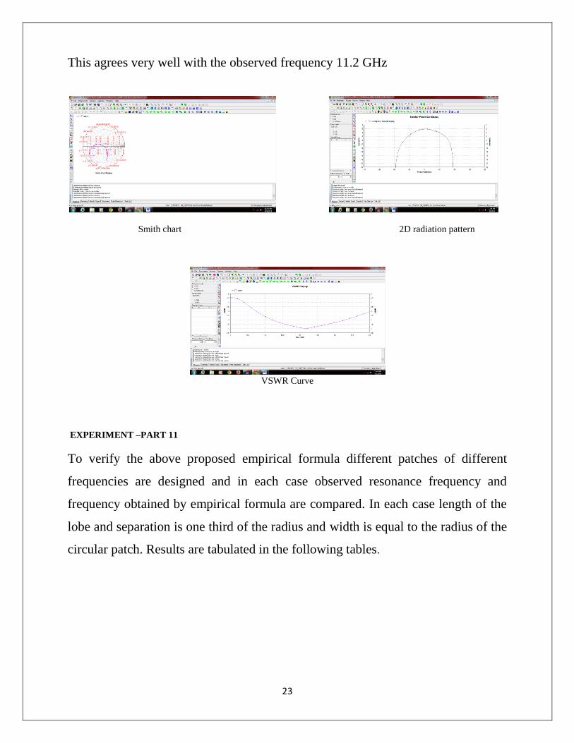
This agrees very well with the observed frequency 11.2 GHz
Smith chart 2D radiation pattern
VSWR Curve
EXPERIMENT –PART 11
To verify the above proposed empirical formula different patches of different
frequencies are designed and in each case observed resonance frequency and
frequency obtained by empirical formula are compared. In each case length of the
lobe and separation is one third of the radius and width is equal to the radius of the
circular patch. Results are tabulated in the following tables.

24
Table 1
Patch Radius R in mm
Length In mm
Width in mm
Separation In mm
Resonance frequency of circular patchIn HzF1
1 3.9 1.3 3.9 1.3 11
2 4.3 1.43 4.3 1.43 9.98
3 4.5 1.5 4.5 1.5 9.53
4 5.1 1.7 5.1 1.7 8.41
5 6 2 6 2 7.15
Table 2
Patch
Resonance frequency as per the width of the lobIn GHz F2
Resonance frequency as per the length of the lobIn GHzF3
Observed frequency for the patch In GHz F0
Frequency as per the empirical formula In GHz F0
Error in %
1 23.85 56.30 11.25 11.6 3
2 21.63 51.18 11.4 10.57 7
3 20.67 48.8 10.9 10.13 7
4 18.23 43.05 10 9.02 9
5 15.50 36.6 7.7 7.75 .6
Following (fig 7) is the graph comparing the observed and theoretical resonance frequencies.
Fig 7
0
2
4
6
8
10
12
14
0 2 4 6
reso
nan
ce f
req
ue
ncy
in G
Hz
trial no
observed
as per formula

25
FURTHER STUDY
Similar experiment can be performed for different patches of different frequencies,
resonance frequencies obtained by IE3D simulation can be compared with the
value obtained by empirical formula and a relevant theory can be developed
RESULT AND CONCLUSION
Analysis revealed that addition of patches enhanced the bandwidth by nearly 16
percent.. Addition of patches is the potential method to enhance the bandwidth of
the conventional microstrip antennas. For multi-band applications also, this is
suitable method. Various structures using different types and sizes of the patches,
number of patches, such microstrip antennas can be designed for various
applications. Gap-coupling along with some other bandwidth enhancement
techniques can be used together to produce ultra large bandwidth, and the antennas
can be designed for various wideband applications.
The empirical formula almost holds good for all trials within the experimental
errors. In coming days suitable theory can be developed which may agree very
well with the experimental results.

26
CHAPTER 4
BANDWIDTH ENHANCEMENT WITH ADDITIONAL LOBES
When two rectangular lobes of length 1.5 mm and width 4.5 mm are attached with
a separation of 6 mm(fig 4), the shape resembles APAANA MUDRA the patch
gave a return loss of -40 dB (fig 5)for a resonance frequency of 9.36 GHz at the
same feed point(-.89,-.5) with band width of 14.1%. Thus 69 % increase in BW is
observed. Theoretical interpretations is yet to be carried out
Fig 4
Fig 5

27
EXPERIMENT –PART 11
With the intension of enhancing the bandwidth the patch is kept between two
rectangles as shown above (fig 6)with a gap of 2mm between them.here resonance
frequency of the right rectangular patch is 11 GHz with length 8.13mm and width
10.33 mm.resonance frequency of the left rectangular patch is 9 GHz with length
6.65mm and width 8.45 mm.
When this parasitic patch is excited using IE3D software ,at the feedpoint of
(2.05,-.5) good band width is 19.24% is obtained (fig 7)with a return loss of -36
Db.Thus APAANA MUDRAA Shape between two rectangles gives a bandwidth
enhancement of 36 %. Or overall increase of 130%.
Fig 7

28
FURTHER STUDY
Similar experiment can be performed for different patches of different frequencies;
resonance frequencies obtained by IE3D simulation can be compared
RESULT AND CONCLUSION
Analysis revealed that addition of patches enhanced the bandwidth by nearly130
percent.. Addition of patches is the potential method to enhance the bandwidth of
the conventional microstrip antennas. For multi-band applications also, this is
suitable method. Various structures using different types and sizes of the patches,
number of patches, such microstrip antennas can be designed for various
applications. Gap-coupling along with some other bandwidth enhancement
techniques can be used together to produce ultra large bandwidth, and the antennas
can be designed for various wideband applications.

29
CHAPTER 5
Observations and tabulations
Antenna 1.
Radius =3.9mm.PRANA MUDRA SHAPE.
Antenna shape
Simulated return loss curve
Observations and experimental return loss curve
frequency input output RT dB
10 0.88 0.153 -15.1958
10.1 0.85 0.135 -15.9817
10.2 0.836 0.122 -16.7169
10.3 0.832 0.092 -19.1267
10.4 0.89 0.053 -24.5023
10.5 0.94 0.023 -32.228
10.6 1.011 0.038 -28.4994

30
10.7 1.043 0.072 -23.219
10.8 0.94 0.91 -0.28173
10.9 0.75 0.098 -17.6767
11 0.624 0.106 -15.3976
11.1 0.543 0.116 -13.4068
11.2 0.492 0.142 -10.7935
11.3 0.48 0.155 -9.81819
11.4 0.471 0.13 -11.1816
11.5 0.48 0.081 -15.4551
11.6 0.493 0.024 -26.2527
11.7 0.503 0.001 -54.0314
11.8 0.485 0.011 -32.887
11.9 0.4 0.032 -21.9382
12 0.253 0.038 -16.4667
12.1 0.222 0.036 -15.801
12.2 0.179 0.03 -15.5146
12.3 0.159 0.026 -15.7285
12.4 0.126 0.022 -15.159
12.5 0.133 0.011 -21.6492
12.6 0.114 0.002 -35.1175
12.7 0.094 0.009 -20.3777
12.8 0.075 0.009 -18.4164
12.9 0.048 0.006 -18.0618
13 0.032 0.004 -18.0618
Radiation pattern study
degrees current in µA
0 0
10 0.013
20 0.034
30 0.046
-60
-50
-40
-30
-20
-10
0
11.3 11.4 11.5 11.6 11.7 11.8 11.9 12 12.1 12.2
Series1

31
40 0.058
50 0.068
60 0.076
70 0.071
80 0.065
90 0.064
100 0.068
110 0.067
120 0.058
130 0.035
140 0.009
150 0.008
160 0.001
Experimental values
Antenna 2.
PRAANA MUDRA SHAPE RADIUS=4.5 mm
0
0.02
0.04
0.06
0.08
0 102030405060708090100110120130140150160170
Series1

32
Simulated return loss curve
Observations and experimental return loss curve
frequency output input Ret Loss in dB
8 0.039 0.754 -25.7261
8.1 0.045 0.739 -24.3086
8.2 0.045 0.63 -22.9226
8.3 0.047 0.53 -21.0436
8.4 0.049 0.441 -19.0849
8.5 0.055 0.389 -16.9917
8.6 0.055 0.357 -16.2461
8.7 0.048 0.343 -17.0811
8.8 0.03 0.353 -21.4131
8.9 0.016 0.364 -27.1396
9 0.01 0.386 -31.7317
9.1 0.016 0.455 -29.0778
9.2 0.046 0.522 -21.0983
9.3 0.1 0.606 -15.6495
9.4 0.143 0.698 -13.7704
9.5 0.193 0.804 -12.394
9.6 0.195 0.84 -12.6849
9.7 0.165 0.849 -14.2285
9.8 0.151 0.826 -14.7601
9.9 0.14 0.791 -15.041
10 0.141 0.762 -14.6547
10.1 0.14 0.769 -14.796
10.2 0.139 0.784 -15.026
10.3 0.129 0.862 -16.4984
10.4 0.098 0.929 -19.5358
10.5 0.06 1.016 -24.5748
10.6 0.037 1.077 -29.2803
10.7 0.043 1.065 -27.8776

33
10.8 0.06 0.94 -23.8995
10.9 0.079 0.799 -20.0984
11 0.101 0.726 -17.1323
11.1 0.137 0.663 -13.6959
11.2 0.185 0.639 -10.7666
11.3 0.209 0.592 -9.04351
11.4 0.2 0.591 -9.41115
11.5 0.141 0.581 -12.2991
11.6 0.062 0.575 -19.3455
11.7 0.016 0.588 -31.3051
11.8 0.003 0.6 -46.0206
11.9 0.017 0.583 -30.7044
12 0.06 0.443 -17.365
12.1 0.074 0.388 -14.392
12.2 0.061 0.311 -14.1486
12.3 0.047 0.272 -15.2494
12.4 0.033 0.257 -17.8284
12.5 0.015 0.262 -24.8442
12.6 0.009 0.264 -29.3472
12.7 0.028 0.236 -18.5151
12.8 0.027 0.181 -16.5263
12.9 0.018 0.14 -17.8171
13 0.011 0.094 -18.6347
Radiation pattern
degrees current in µA
0 0.003
10 0.016
-50
-45
-40
-35
-30
-25
-20
-15
-10
-5
0
11.2 11.4 11.6 11.8 12 12.2 12.4
Series1

34
20 0.045
30 0.072
40 0.084
50 0.093
60 0.094
70 0.088
80 0.083
90 0.079
100 0.086
110 0.1
120 0.085
130 0.059
140 0.036
150 0.009
160 0.002
RESULT AND CONCLUSION
In both the antennas there is a good agreement between experimental and
simulated values with respect to return loss,bandwidth etc.
.. Addition of patches is the potential method to enhance the bandwidth of the
conventional microstrip antennas. For multi-band applications also, this is suitable
method. Various structures using different types and sizes of the patches, number
0
0.02
0.04
0.06
0.08
0.1
0.12
0 10 20 30 40 50 60 70 80 90 100110120130140150160170
Series1

35
of patches, such microstrip antennas can be designed for various applications. Gap-
coupling along with some other bandwidth enhancement techniques can be used
together to produce ultra large bandwidth, and the antennas can be designed for
various wideband applications.
PART 2
With the intension of getting still higher band width different antennas of different
mudra shapes as given below are simulated and the results are tabulated. Further
experimental investigations are to be carried out
Table 1 showing different mudras
Sl no
Name Pattern
1. Prana mudra
2. Apana Mudra
3. Jnana Mudra
4. Akasha
Mudra
5. Aditi Mudra
6. Eka Mudra
7. Mrigi Mudra
36
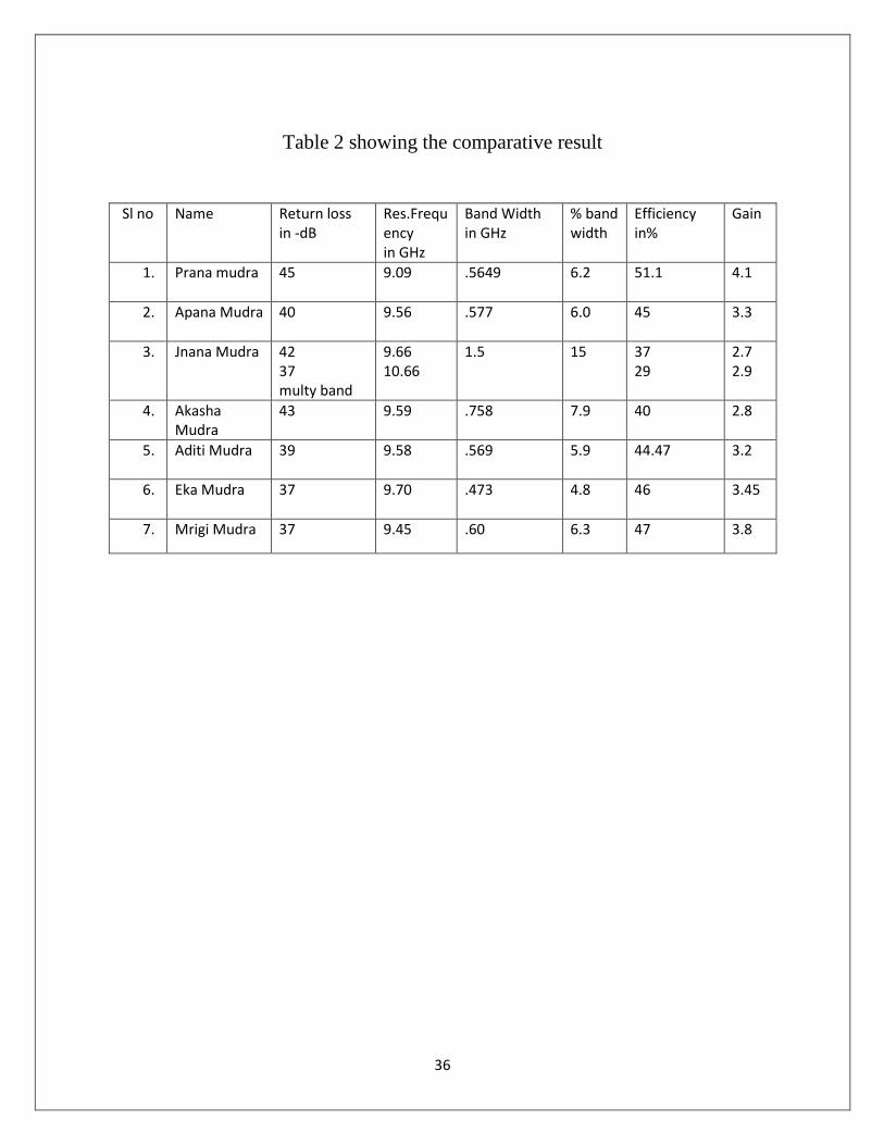
Table 2 showing the comparative result
Sl no Name Return loss in -dB
Res.Frequency in GHz
Band Width in GHz
% band width
Efficiency in%
Gain
1. Prana mudra 45 9.09 .5649 6.2 51.1 4.1
2. Apana Mudra 40 9.56 .577 6.0 45 3.3
3. Jnana Mudra 42 37 multy band
9.66 10.66
1.5 15 37 29
2.7 2.9
4. Akasha Mudra
43 9.59 .758 7.9 40 2.8
5. Aditi Mudra 39 9.58 .569 5.9 44.47 3.2
6. Eka Mudra 37 9.70 .473 4.8 46 3.45
7. Mrigi Mudra 37 9.45 .60 6.3 47 3.8

37
SUMMARY OF FINDINGS
1. The analysis reveals that in the gap coupling method Return loss increased to -
46 dB for 2.5mm gap. For circular patch it is only -33dB. And the bandwidth
increased by 16% The gap-coupling is the potential method to enhance the
bandwidth of the conventional microstrip antennas..
2. The systematic study of variation of return loss with the gap between the patches
reveals that Return loss decreases with the gap between the patches and reaches a
maximum of -46 dB for 2.5mm gap. For circular patch it is only -33dB.Band width
decreases with the gap, Resonance frequency varies with the gap.
3. Analysis revealed that addition of patches enhanced the bandwidth by nearly 16
percent.. Addition of patches is the potential method to enhance the bandwidth of
the conventional microstrip antennas.
The empirical formula almost holds good for all trials within the experimental
errors. In coming days suitable theory can be developed which may agree very
well with the experimental results.
4. Analysis revealed that addition of patches enhanced the bandwidth by nearly130
percent.There is a good agreement between experimental and simulated values
with respect to return loss, bandwidth etc.
Addition of patches is the potential method to enhance the bandwidth of the
conventional microstrip antennas. For multi-band applications also, this is suitable
method. Various structures using different types and sizes of the patches, number
of patches, such microstrip antennas can be designed for various applications. Gap-

38
coupling along with some other bandwidth enhancement techniques can be used
together to produce ultra large bandwidth, and the antennas can be designed for
various wideband applications.
Further study
Experiments will be carried out with the above mudrashapes and results are
compared and further investigation is done to have ultra high band antenna.

39
REFERENCES
[1].I J Bahal and B Bhatia”microstrip antenna”Artec House,1980
[2].Frank Zavosh”improving the performance of the microstrip patch antennas “IEEE Trans Antennas
propogation vol 38,no 4,pp 7-11,aug,1996
[3].Howel J Q “microstrip antennas and Microstrip phased arrays”IEE Transaction on antennas and
propogation vol-ap22,pp74-78,1974
[4].K R Carver,”microstrip antenna technology”IEEE Trans.antennas propogation vol 29,pp 2-24
aug,1981
[5] I.J Bahl and Bhartia, "Micro strip Antennas", Artech House, Dedham,MA, 1980
[6] J.R James, P.S Hall and C.Wood, "Microstrip antenna-theory anddesign", London, UK, Peter
Peregrinus Ltd., IEE, 1981.
[7] C.A Balanis, "Antenna Theory: Analysis and design", Harper and RowPublishers, New York, 1982.
[8] L.V.Blake, "Antennas, artech House Dedham, MA, 1984.63
[9) John D.Kraus, "Antenna", Me Graw -Hill International Editions, 2edition, 1988.
[10) K.C. Gupta and Abdelaziz BenalIa, "Microstrip antenna design", ArtechHouse, Inc.Norwood MA,
1988.
[11) J.RJames and P.S Hall, "Hand book of microstrip antennas", PeterPeregrinus Ltd., IEE Engieners IV
series, 1989.
[12) AlIen Taflove, "Computational electrodynamics, The finite - differencetime -domain method",
Artech House, Norwood MA 1995.
[13] Kai Fong Lee and Wei Chen, "Advances in microstrip and printed antennas', John Wiley & Sons, Inc.
New York 1997.
[14] IE3D User's manual, Release 7, Zeland Software, Inc.December 1999.
[15] Fidelity User's manual, Release 3, Zeland Software, April 2000.

40
[16] Rames Garg, Prakash Bhartia, Inder Bahl and Apisak Ittipiboon,"Microstrip antenna design
handbook", Artech House, London, 2001.
[17] E.V.Byron, "A new Flush Mounted Antenna Element for Phased Array application", Proc.Phased
Array Antenna Symp., pp. 187-192, 1970
[18] Y. Dakeya, T. Suesada, K. Asakura, N. Nakajima, and H. Mandai, Chip multilayer antenna for 2.45
GHz-Band Application using LTCC technology, IEEE MTT-S Int 3 (2000), 1693-1696.
[19] M. Chair, K.M. Luk, and K.F. Lee, Miniature multilayer shorted patch antenna, Electron Lett 36
(2000), pp 3 and 4.
[20] M. Ali, S.S. Stuchly, and K. Caputa, A wideband dual meander sleeve antenna, Antennas Propagat
Soc Int S ymp 3 (1996), 1598-1601.
[21] D. Liu, "A dual-band antenna for cellular applications," in Proc. IEEE Antennas Propagat. Soc. 1nt.
Symp. , vol. 2, June 21-26, 1998, pp. 786-789.
[22] R. Schlub, D. V. Thiel, lW. Lu, and S. G. O'Keefe, "Dual-band six-element switched parasitic array for
smart antenna cellular communications systems,"Electron. Lett., vol. 36, pp. 1342-1343,2000.
[23] D. Liu, "A multi branch monopole antenna for dual-band cellular applications," in Proc. IEEE
Antennas Propagation Soc. 1nt. Symp. , vol. 3, July 11-16,1999, pp. 1578-1581.64
[24] C. T. P. Song, P. S. Hall, H. Ghafouri-Shiraz, and D. Wake, "Multi-circular loop monopole antenna,"
Electron. Lett., vol. 36, pp. 391-393,2000.
[25] E. Lee, P. S. Hall, and P. Gardner, "Dual band folded monopole/loop antenna for terrestrial
communication system," Electron. Lett., vol. 36,pp. 1990-1991,2000.
[26] P. Eratuuli, P. Haapala, and P. Vainikainen, "Dual frequency wire antenna," Electron. Lett., vol. 32,
pp. 1051-1052,1996.
[27] H. Nakano, N. Ikeda, Y. Y.Wu, R. Suzuki, H. Mimaki, and J. Yamauchi, "Realization of dual-frequency
and wide-band VSWR perfonnances using nonnal-mode helical and inverted-F antennas," IEEE Trans.
Antennas Propagat., vol. 46, pp. 788-793, June 1998.

41
[28] H. M. Chen, "Micro strip-fed dual-frequency printed triangular monopole," Electron. Lett., vol. 38,
pp. 619-620, 2002.
[29] F. S. Chang, S. H. Yeh, and K. L. Wong, "Planar monopole in wrapped structure for low-profile
GSM/DCS mobile phone antenna," Electron. Lett., voL 38, pp. 499-500, 2002.
[30] A CPW-Fed Dual-Frequency Monopole Antenna Homg-Dean Chen, Member, IEEE, and Hong-Twu
Chen. Member. IEEE
[31] A Novel Printed Monopole Antenna with a Square Conductor-Backed Parasitic Plane for Dual-Band
WLAN Applications 'c. Y. Pan, C. H Huang and T. S. Homg Department of Electrical Engineering, National
Sun Yat-Sen University Kaohsiung 804, Taiwan.
[32] M. Ali and G. J. Hayes, "Analysis of integrated inverted-F antennas for Buletooth applications." 2000
IEEE AP-S Conf Antenna Propagation for Wireless Communication, Waltham, MA, pp. 21-24.
[33] Y. L. Kuo and K. L. Wong, "Coplanar waveguide-fed folded inverted-F antennas for UMTS
application." Microwave Opt. Technol. Lett. vol. 32 pp.
[34].antenna band width electronic communication systems-fifth edition-Wayne Tomasi p 621
[35].carver K R and Mink J W “microstrip antenna technology “ ibid.pp2-24
[36].microstrip patch antennas “a designer guide” by Rodney B water house ,1999
[37].Kanda, ”Iris fed millimeter wave rectangular antenna.” IEEE Electromagnetic
computability vol.27, no. 4,pp212-220,1985.