Embed Size (px)
Citation preview

MiniRISC™CW400x
Microprocessor CoreTechnical Manual
Order Number C14030.A

ii
This document contains data derived from functional simulations and perfor-mance estimates. LSI Logic has not verified either the functional descriptions, orthe electrical and mechanical specifications using production parts.
Document DB14-000009-01, Second Edition (October 1996)This document describes Revision B of LSI Logic Corporation’s MiniRISC™CW400x Microprocessor Cores and will remain the official reference source forall revisions/releases of this product until rescinded by an update.
To receive product literature, call us at 1-800-574-4286 (or 415-940-6877outside the U.S. and Canada) and ask for Department JDS; or visit us athttp://www.lsilogic.com.
LSI Logic Corporation reserves the right to make changes to any products hereinat any time without notice. LSI Logic does not assume any responsibility or lia-bility arising out of the application or use of any product described herein, exceptas expressly agreed to in writing by LSI Logic; nor does the purchase or use ofa product from LSI Logic convey a license under any patent rights, copyrights,trademark rights, or any other of the intellectual property rights of LSI Logic orthird parties.
Copyright © 1995, 1996 by LSI Logic Corporation. All rights reserved.
TRADEMARK ACKNOWLEDGMENTLSI Logic logo design, MDE, Modular Design Environment, and CoreWare areregistered trademarks and C-MDE, MiniRISC, MiniSIM, Right-First-Time, andSelf-Embedding are trademarks of LSI Logic Corporation. MIPS is a trademarkof MIPS Technologies, Inc. SPARC is a registered trademark of SPARC Interna-tional, Inc. UNIX is a registered trademark of X/Open Company Limited. Verilogis a registered trademark of Cadence Design Systems, Inc. All other brand andproduct names may be trademarks of their respective companies.
Preface iii
Preface
This book is the primary reference and Technical Manual for theMiniRISC CW400x Microprocessor Core. It contains a complete func-tional description for the core and includes complete physical and elec-trical specifications for the core.
Audience This document assumes that you have some familiarity with microproces-sors and related support devices. This book is written for:
♦ Engineers and managers who are evaluating the processor for pos-sible use in a system
♦ Engineers who are designing the processor into a system
Organization This document has the following chapters and appendixes:
♦ Chapter 1, Introduction
♦ Chapter 2, Function
♦ Chapter 3, Signals
♦ Chapter 4, Instructions
♦ Chapter 5, Exception Processing (CP0)
♦ Chapter 6, Required External Modules
♦ Chapter 7, Interfaces
♦ Chapter 8, Methodologies and Layout Guidelines
RelatedPublications
MiniRISC™ Building Blocks Technical Manual, Doc No. DB14-000022-00Order Number C14031

iv Preface
CW33300 Enhanced Self-Embedding™ Processor Core User’s Manual,Order No. C14014
LR33000 Family Instruction Set Guide, Doc No. MT72-000102-99 OrderNumber J14029
ConventionsUsed in ThisManual
The first time a word or phrase is defined in this manual, it is italicized.
The following signal naming conventions are used throughout thismanual:
♦ A level-significant signal that is true or valid when the signal is LOWalways has an overbar ( ) over its name and ends with an “N.”
♦ An edge-significant signal that initiates actions on a HIGH-to-LOWtransition always has an overbar ( ) over its name and ends withan “N.”
♦ A level-significant signal that is true or valid when the signal is HIGHalways ends with a “P.”
♦ An edge-significant signal that initiates actions on a LOW-to-HIGHtransition always ends with a “P.”
The word assert means to drive a signal true or active. The worddeassert means to drive a signal false or inactive.
Hexadecimal numbers are indicated by the prefix “0x” before thenumber—for example, 0x32CF. Binary numbers are indicated by a sub-scripted “2” following the number—for example, 0011.0010.1100.11112.

Contents v
Contents
Chapter 1 Introduction1.1 System Overview 1-11.2 Features Summary 1-21.3 MiniRISC Product Family 1-31.4 CoreWare Program 1-4
1.4.1 CoreWare Building Blocks 1-41.4.2 Design Environment 1-41.4.3 Expert Support 1-5
Chapter 2 Function2.1 Microprocessor Overview 2-12.2 Functional Differences from the R3000 and the R4000
CPUs 2-32.3 Pipeline Architecture 2-42.4 Load Delay Slot 2-52.5 Branch Delay Slot 2-52.6 Load Scheduling Support 2-72.7 WAITI Instruction: Power Saving Feature 2-9
Chapter 3 Signals
Chapter 4 Instructions4.1 Instruction Formats 4-14.2 CW400x Opcode Bit Encoding 4-34.3 Instruction Summary 4-74.4 Load and Store Instructions 4-94.5 Computational Instructions 4-124.6 Jump and Branch Instructions 4-14

vi Contents
4.7 Branch Likely Instructions 4-164.8 Special Control Instructions 4-184.9 Trap Instructions 4-194.10 Coprocessor Instructions 4-204.11 System Control Coprocessor (CP0) Instructions 4-21
Chapter 5 Exception Processing (CP0)5.1 Exception Handling Registers 5-1
5.1.1 Status Register (R12) 5-25.1.2 Cause Register (R13) 5-45.1.3 Exception Program Counter (EPC) Register (R14) 5-75.1.4 Processor Revision Identifier (PRId) Register (R15) 5-7
5.2 Exception Processing 5-95.2.1 Exception Vector Locations 5-115.2.2 Status Register Mode Bits and Exception
Processing 5-115.2.3 System Control Coprocessor (CP0) Function 5-125.2.4 Register Accesses 5-135.2.5 Exception Handling 5-13
5.3 Exception Description Details 5-235.3.1 Address Error Exception 5-235.3.2 Breakpoint Exception 5-245.3.3 Bus Error Exception 5-255.3.4 Coprocessor Unusable Exception 5-265.3.5 Interrupt Exception 5-285.3.6 Overflow Exception 5-285.3.7 Reserved Instruction Exception 5-295.3.8 Reset Exception 5-305.3.9 System Call Exception 5-315.3.10 Trap Exception 5-32
Chapter 6 Required External Modules6.1 Global Output Enable Module (GOE) 6-1
6.1.1 Function 6-16.1.2 Signals 6-76.1.3 Connecting to the CW400x and Building Blocks 6-13
6.2 MMU Stub 6-14

Contents vii
6.2.1 Function 6-146.2.2 Signals 6-156.2.3 Connecting to the CW400x 6-17
Chapter 7 Interfaces7.1 CBus Interface 7-1
7.1.1 Bus Stealing 7-17.1.2 Interface Signals 7-17.1.3 Operation and Functional Waveforms 7-2
7.2 FlexLink Interface 7-137.2.1 Interface Signals 7-147.2.2 Computational Unit Instructions 7-167.2.3 Operation and Functional Waveforms 7-18
Chapter 8 Methodologies and Layout Guidelines8.1 Clocking Methodology 8-1
8.1.1 Duty Cycle 8-28.1.2 Local Clock Buffers 8-28.1.3 Gated Clocks 8-38.1.4 Delayed Clocks 8-38.1.5 Hold Time Margin 8-4
8.2 Scan Methodology 8-48.2.1 Methodology 8-58.2.2 Regeneration (Recommended Methodology) 8-68.2.3 Core ATPG Shell 8-78.2.4 CW400x ATPG Guidelines 8-98.2.5 MMU ATPG Guidelines 8-108.2.6 MDU ATPG Guidelines 8-10
8.3 Layout Guidelines 8-118.3.1 Hardmac I/O Placement 8-118.3.2 Data Bus 8-148.3.3 CW400x Placement 8-148.3.4 BBCC Placement 8-168.3.5 Computational Unit Placement 8-178.3.6 MMU Placement 8-188.3.7 Coprocessor Placement 8-208.3.8 Global Output Enable (GOE) Placement 8-22

viii Contents
8.3.9 Cache RAMs Placement 8-238.3.10 Tagmatch Placement 8-248.3.11 Write Buffer Placement 8-258.3.12 B-Bus Device Placement 8-26
Appendix A Structural ALU Improper Unknown Value (X) Handling
Customer Feedback
Figures 1.1 CW400x in a Typical System 1-22.1 CW400x Internal Block Diagram 2-22.2 CW400x Pipeline 2-42.3 CW400x Pipeline with X2 Stall Cycle 2-42.4 Three Consecutive Non-Load/Store Instructions 2-42.5 Load/Store Instruction 2-42.6 Two Consecutive Load/Store Instructions 2-52.7 WB to X1 Stage Bypass (No Load Delay Slot Necessary) 2-52.8 Branch Taken 2-62.9 Branch Not Taken 2-62.10 Branch Likely Taken 2-72.11 Branch Likely Not Taken 2-72.12 Scheduled Load Instruction 2-82.13 Scheduled Load Followed by a Second Load 2-84.1 I-Type (Immediate) Instruction 4-24.2 J-Type (Jump) Instruction 4-24.3 R-Type (Register) Instruction 4-24.4 Byte Specifications for Loads/Stores 4-94.5 WAITI Instruction Waveforms 4-225.1 Status Register 5-35.2 Cause Register 5-55.3 EPC Register 5-75.4 PRId Register 5-85.5 Status Register Changes During Exception Recognition 5-125.6 Restoring Control from Exceptions (RFE Instruction) 5-125.7 Typical Pipeline Flow 5-145.8 Branch Likely, Branch Not Taken (X1 Stage) 5-155.9 X1 Stage Exception (System Call) 5-16

Contents ix
5.10 WB Stage Exception (Overflow) 5-165.11 IF Stage Exception (TLB Miss, Instruction) 5-175.12 Reset Exception (Special Case) 5-175.13 X2 Stage Exception (TLB Miss, Data Load) 5-185.14 External Interrupt Signalled During X2 Stage 5-195.15 Instruction Bus Error, (X1 Stage) 5-195.16 Data Bus Error, (WB Stage) 5-205.17 Multiple CKILLMEMP Assertion 5-205.18 External Coprocessor (FPU) Interrupt (Interrupt Not Taken) 5-215.19 External Coprocessor (FPU) Interrupt (Interrupt Taken) 5-225.20 Branch Likely Delay Slot Invalidation 5-235.21 Branch Target Address Calculation 5-306.1 Basic Functional GOE Design Logic 6-36.2 Improved Timing GOE Design Logic 6-56.3 Final GOE Design Logic 6-66.4 Creation of RUN_INN 6-76.5 Creation of CPIPE_RUNN 6-76.6 GOE Module Attachments 6-136.7 MMU Stub Hard Address Mapping (Hard Map) 6-156.8 MMU Stub Attachments 6-187.1 Instruction Fetch Examples 1 7-47.2 Instruction Fetch Example 2 7-57.3 Data Load Example 1 7-77.4 Data Load Example 2 7-87.5 Data Load Example 3 7-97.6 Data Load Example 4 7-107.7 Data Store Example 1 7-127.8 Data Store Examples 2 7-137.9 Opcodes 7-167.10 R-Type Arithmetic (Extended) Instruction 7-177.11 I-Type Arithmetic (Extended) Instruction 7-187.12 Computational Unit Write to CW400x CPU Register 7-207.13 Computational Unit Single-Cycle Killed by CKILLXP 7-217.14 Computational Unit Operation, Stalled and Killed 7-227.15 Two-Cycle Computational Unit Operation (Example 1) 7-237.16 Two-Cycle Computational Unit Operation (Example 2) 7-247.17 Three-Cycle Computational Unit Operation 7-257.18 Stalled Two-Cycle Computational Unit Operation 7-26

x Contents
7.19 Two-Cycle CU Operation with Writeback (Example 1) 7-277.20 Two-Cycle CU Operation with Writeback (Example 2) 7-288.1 Two-level Clock Distribution Network 8-28.2 Gated Clock Logic 8-38.3 Methodology Flowchart 8-58.4 Input Pin Schematic for ATPG Shell 8-88.5 Output Pin Schematic for ATPG Shell 8-88.6 Bidirectional Pin Schematic for ATPG Shell 8-98.7 CW400x Hardmac 8-128.8 BBCC Hardmac 8-138.9 MDU Hardmac 8-148.10 CW400x Placement Example 8-158.11 BBCC Suggested Placement 8-168.12 Computational Unit Suggested Placement 8-178.13 MMU (with no CU) Suggested Placement 8-188.14 MMU (with CU) Suggested Placement 8-198.15 Coprocessor Placement Example 1 8-208.16 Coprocessor Placement Example 2 8-208.17 Coprocessor Placement Example 3 8-218.18 Global Output Enable Suggested Placement 8-228.19 Cache RAMs Placement Example 8-238.20 Tagmatch Placement 8-248.21 Write Buffer Placement Example 8-258.22 B-Bus Device Placement Example 8-26
Tables 3.1 Signal Summary 3-14.1 Shading Key for Tables 4.2 through 4.6 4-34.2 Major Opcode (op) Bit Encoding 4-44.3 SPECIAL Minor Opcode funct Bit Encoding 4-44.4 REGIMM Minor Opcode rt Bit Encoding 4-54.5 COPz (z = 0, 1, 2, 3) rs Minor Opcode Bit Encoding 4-54.6 COPz (z = 0, 1, 2, 3) rt Minor Opcode Bit Encoding 4-54.7 COP0 Minor Opcode funct Bit Encoding
(Bits[25:24] = 1x2) 4-64.8 COPz (z = 1, 2, 3) Minor Opcode funct Bit Encoding
(Bits[25:24] = 1x2) 4-64.9 CW400x Instructions 4-84.10 Load and Store Instruction Summary 4-10
Contents xi
4.11 ALU Immediate Arithmetic Instruction Summary 4-124.12 Three-Operand, Register-Type Arithmetic Instruction
Summary 4-134.13 Shift Instruction Summary 4-144.14 Jump and Branch Instruction Summary 4-154.15 Branch Likely Instruction Summary 4-174.16 Special Control Instruction Summary 4-184.17 Trap Instruction Summary 4-194.18 Coprocessor Instruction Summary 4-204.19 CP0 Instruction Summary 4-215.1 Exception-Processing Register Addresses 5-25.2 CW400x Exceptions 5-95.3 Exception Vector Locations 5-115.4 CP0 Register Addresses 5-135.5 Exception Priority 5-146.1 Output Enable Decoding 6-47.1 CW400x CBus Interface Signals 7-27.2 CW400x FlexLink Interface Signals 7-147.3 System Logic FlexLink Interface Signals 7-158.1 Driver Type and Module Name 8-38.2 Hold Time Margin 8-4

xii Contents

1-1
Chapter 1Introduction
This chapter introduces the LSI Logic MiniRISC™ CW400x Microproces-sor Core.
This chapter contains the following sections:
♦ Section 1.1, “System Overview”
♦ Section 1.2, “Features Summary”
♦ Section 1.3, “MiniRISC Product Family”
♦ Section 1.4, “CoreWare Program”
1.1SystemOverview
The MiniRISC CW400x Microprocessor Core family, components of theLSI Logic CoreWare® Library, are exceptionally compact, high-perfor-mance microprocessors compatible with the MIPS R4000, including allof the MIPS-I and most of the MIPS-II Instruction Set (for details seeChapter 4). The CW400x can be easily designed into a wide range ofproducts. The CW400x can be combined with industry standard coresand proprietary functional building blocks to create a completely custom-ized embedded system on a chip. LSI Logic currently provides the fol-lowing optional building blocks:
♦ Multiply/Divide Unit (MDU)
♦ Memory Management Unit (MMU)
♦ Basic Bus Interface Unit and Cache Controller (BBCC)
♦ Timer
These building blocks are described in the MiniRISC Building BlocksTechnical Manual. System designers can use these building blocks(unmodified or modified) and/or add their own customized logic to theCW400x Core.

1-2 Introduction
LSI Logic also provides the following external modules (for more informa-tion, see Chapter 6):
♦ Global Output Enable Module (GOE)
♦ MMU Stub (to be used if there is no MMU present)
The CW400x has been optimized for low-power and cost-sensitive appli-cations such as portable telecommunications, games, and consumermultimedia systems.
The CW400x FlexLink Interface allows customer-specific microprocessorinstructions. The core implements a simple three-stage pipeline and pro-vides a single cache/memory interface for both instructions and data.With a system clock of 60 MHz, the performance of the CW400x is esti-mated at 45 MIPS sustained. The core implements full scan to achievegreater than 99% fault coverage.
Figure 1.1 shows the CW400x Microprocessor Core and how it interfaceswith system logic in a typical customer design.
Figure 1.1CW400x in a TypicalSystem
1.2FeaturesSummary
The CW400x has the following features:
♦ Fully compatible with the MIPS-I and most of the MIPS-II InstructionSet
♦ CW400x-specific Instructions
CW400x
MMU or
Coprocessor
CBus
RAM/ROM
CacheDRAM
DMA
Timer
BIU andCache
Controller(BBCC)
Write Buffer
MDU
BBusCBusInterface
Controller
Controller
FlexLinkInterface
GOE
MMU Stub

MiniRISC Product Family 1-3
♦ Configurable, compact, modular design and unified bus architecture
♦ Eliminates the need for a load delay slot
♦ Simple three-stage pipeline: Fetch, Execute, and Writeback
♦ Load/Store Instructions, MFCz, MTCz, CFCz, and CTCz execute intwo cycles
♦ All other instructions execute in one cycle
♦ WAITI (Wait for Interrupt) Instruction for power savings
♦ Powerful FlexLink Interface allows customer-specific microprocessorinstructions
♦ High-performance Coprocessor Interface for user-definable copro-cessors and high-performance hardware FPU
♦ 32-bit memory and cache interfaces
♦ Optional building blocks: Timer, MMU, MDU, BBCC
♦ 3.3-volt operation
♦ Implementation of full scan to achieve 99% fault coverage
♦ 60-MHz worst case commercial maximum clock rate using high-performance 0.5-micron process
♦ 60 MIPS peak, 45 MIPS sustained with standard compiled MIPScode at 60 MHz
♦ Models available: performance and software development, VHDL,Verilog, and gate-level, timing-accurate models
♦ Compatible with the full range of MIPS, third party software develop-ment, and System Verification Environment tools
♦ Fully testable in embedded ASIC designs
♦ MR4001 Lead Vehicle chip available with cache, MMU, and MDU
1.3MiniRISCProduct Family
The MiniRISC product family has all the necessary tools to develop asystem on a chip, including LSI Logic’s MiniSIM™ architectural simulator,Verilog and VHDL models, a System Verification Environment, a PROMmonitor, third party software support, and a core bond-out chip foremulation.
1-4 Introduction
1.4CoreWareProgram
The CoreWare program offers a new approach to system design.Through the CoreWare program, LSI Logic gives customers the ability tocombine the CW400x Microprocessor Core with other cores on a singlechip to create products uniquely suited to the customer’s applications.This approach – combining high-performance building blocks, sophisti-cated design software, and expert support – provides unparalleleddesign flexibility and allows designers to create high-quality, leading-edgeproducts for a wide range of markets.
The CoreWare program consists of three main elements: a library ofcores, a design development and simulation package, and expert appli-cations support. The CoreWare library contains a wide range of complexcores based on accepted and emerging industry standards from high-speed interconnect, digital video, DSP, and others. LSI Logic provides acomplete framework for device and system development and simulation.LSI Logic’s advanced ASIC technologies consistently produce Right-First-Time™ silicon. LSI Logic’s in-house experts provide design supportfrom system architecture definition through chip layout and test vectorgeneration.
1.4.1CoreWareBuilding Blocks
The CoreWare building blocks include elements based on the LSI Logichigh-performance standard products as well as other, industry-standardproducts. The CoreWare building blocks, which include embedded MIPSand SPARC processors, bus interface controllers, and a family of floating-point processors, are fully supported library elements for use in the LSILogic hardware development environment. Note that the building blocksinclude gate-level simulation models with timing information, so design-ers can accurately simulate device performance and trade off variousimplementation options. In addition to gate-level simulation models, thebuilding blocks also include behavioral simulation models.
1.4.2DesignEnvironment
LSI Logic’s C-MDE™ (Concurrent-Modular Design Environment®) designsystem and LSI ToolKit provides a complete framework for device andsystem development. The LSI ToolKit provides front-end support, whilethe C-MDE provides backend support.
The new ASIC families are supported by LSI Logic’s comprehensivesystem-on-a-chip design methodology. This design methodology usesboth internally developed and industry-standard tools integrated with the

CoreWare Program 1-5
LSI ToolKit. LSI ToolKit is a system of software and libraries that allowengineers to use third-party software to access LSI Logic's technology.Designers can select from a suite of industry-standard simulators,synthesizers, timing analyzers and test tools seamlessly integrated intoa common environment for verification and sign-off.
1.4.3Expert Support
LSI Logic’s in-house experts support the CoreWare program with high-level design and market experience in a wide variety of application areas.These experts provide design support from system architecture definitionthrough chip layout and test vector generation. They help determine howmany functions to integrate on a single chip, trading off functionality ver-sus cost to find the most cost-effective solution. When the trade-offs arecomplete, the designer and LSI Logic’s applications engineers implementand test the design using C-MDE and theCoreWare building blocks.

1-6 Introduction

2-1
Chapter 2Function
This chapter describes the function of the MiniRISC CW400x Micropro-cessor Core. It contains the following sections:
♦ Section 2.1, “Microprocessor Overview”
♦ Section 2.2, “Functional Differences from the R3000 and the R4000CPUs”
♦ Section 2.3, “Pipeline Architecture”
♦ Section 2.4, “Load Delay Slot”
♦ Section 2.5, “Branch Delay Slot”
♦ Section 2.6, “Load Scheduling Support”
♦ Section 2.7, “WAITI Instruction: Power Saving Feature”
For an introduction to Memory Space see Section 6.2, “MMU Stub”
2.1MicroprocessorOverview
The MiniRISC CW400x Microprocessor Core is an exceptionally com-pact, high-performance microprocessor compatible with the MIPS R4000(all of the MIPS-I and most of the MIPS-II Instruction Set). Figure 2.1 isan internal block diagram of the MiniRISC CW400x Microprocessor Core.Descriptions of the internal blocks follow the figure.

2-2 Function
Figure 2.1CW400x InternalBlock Diagram
The Register File contains the general-purpose registers. It suppliessource operands to the execution units and handles the storage ofresults to target registers. The System Control Coprocessor (CP0) pro-cesses exceptions (which includes interrupts). The Arithmetic LogicalUnit (ALU) performs arithmetic and logical operations, as well asaddress calculations. The Shifter performs shift operations.
The CBus Interface passes data to and from the core. It allows theattachment of up to three tightly coupled special-purpose coprocessorsthat enhance the microprocessor’s general purpose computationalpower. Using this approach, high-performance, application-specific hard-ware can be made directly accessible to a programmer at the instruction-set level. For example, a coprocessor might offer accelerated bit-mappedgraphics operations or real-time video decompression. The interface alsoallows the attachment of a Memory Management Unit (MMU) and a BusInterface Unit (BIU).
The FlexLink Interface allows the logic designer to insert specializedarithmetic instructions into the Microprocessor Core. Adding a Computa-tional Unit (for instance LSI Logic’s Multiply/Divide Unit) to the FlexLinkInterface, for instance, allows the logic designer to insert a DSP-typeinstruction. This interface can handle one-cycle operations or multicycleoperations.
Register File
CP0 ALU Shifter
FlexLink Interface
CBus Interface

Functional Differences from the R3000 and the R4000 CPUs 2-3
2.2FunctionalDifferencesfrom the R3000and the R4000CPUs
1. The CW400x is not a Harvard architecture. The R3000 and R4000Microprocessors are Harvard architectures. The CW400x provides asingle cache/memory interface instead of interfaces for both instruc-tion cache and data cache, cutting the I/O count almost in half. Over-head outside of the CW400x associated with address buses, databuses and RAMs is dramatically reduced.
2. The CW400x uses a three-stage pipeline (Fetch, Execute, and Write-back) instead of the R3000 five-stage pipeline or the R4000 seven-stage pipeline. The R3000 RD and ALU Stages are merged into asingle Execute Stage. Since it is not a Harvard architecture, theCW400x does not need a MEM Stage like the R3000 CPU. Instead,the CW400x stalls internally in the Execute Stage and does thememory access in a second Execute Cycle.
3. The CW400x is a 32-bit architecture like the R3000. The R4000 is a64-bit machine with 32-bit programmability.
4. The CW400x CP0 is similar to the R3000 CP0. In particular, thefields within the CP0 Registers that are related to exception handlingare like the R3000, and the CW400x implements only the kernel anduser operating modes (no supervisor mode).
5. The CW400x implements the MIPS-I and MIPS-II Branch Likely andTrap Instructions. Other MIPS-II Instructions (Load Linked, StoreConditional, Sync, Load and Store Double Coprocessor Instructions)cause Reserved Instruction Exceptions.
6. The CW400x contains no multiply or divide circuitry. Multiply anddivide circuitry would significantly increase the area of the CW400x.Since many applications do not require high performance multiplyand divide, the CW400x’s FlexLink Interface is designed to supportoptional multiply/divide units with differing performance. Refer toSection 7.2, “FlexLink Interface” for more details.

2-4 Function
2.3PipelineArchitecture
The CW400x implements a three-stage pipeline (Instruction Fetch, Exe-cute, and Writeback). Figures 2.2 and 2.3 show the two forms of theCW400x three-stage pipeline.
Figure 2.2CW400x Pipeline
Figure 2.3CW400x Pipelinewith X2 Stall Cycle
The execution of a single CW400x instruction consists of the followingpipeline stages:
1. Instruction Fetch – The core fetches the instruction (IF).
2. Execute – The core executes all ALU instructions, resolves condi-tional branches, and calculates Load and Store addresses (X1). Thecore transfers Load and Store data from external memory or cache(performs memory accesses) in a second Execute (Stall) Cycle (X2).
3. Writeback – The core writes the results into the Register File (WB).
Figures 2.4 through 2.6 show instruction pipeline examples.
Figure 2.4Three ConsecutiveNon-Load/StoreInstructions
Figure 2.5Load/StoreInstruction
X1 X2 WB
Execute WritebackInstruction Fetch
IF
IF X1 WB
IF X1 WB
IF X1 WB
1. Non-Load/Store Instruction
2. Non-Load/Store Instruction
3. Non-Load/Store Instruction
IF X1
IF X1 X2
IF X1 WB
WB
WB
1. Non-Load/Store Instruction
2. Load/Store Instruction
3. Non-Load/Store Instruction

Load Delay Slot 2-5
Figure 2.6Two ConsecutiveLoad/Store Instructions
2.4Load Delay Slot
The CW400x does not require a load delay slot.
In the five-stage R3000 architecture, the load delay slot refers to theinstruction following any load. The instruction following a load cannot usethe data from that load. Software must ensure that the instruction in theload delay slot does not depend on the data of the load.
Since the CW400x is a three-stage pipeline, its architecture does notrequire this restriction. All instructions, including load data dependentinstructions may follow a load.
Figure 2.7 shows an example of a load followed by an instruction depen-dent on the load data. A load delay slot is unnecessary because datafrom the load is valid in its WB Stage and can be bypassed to the fol-lowing instruction’s X1 Stage.
Figure 2.7WB to X1 StageBypass (No LoadDelay SlotNecessary)
2.5Branch DelaySlot
Because they are pipelined architectures, the CW400x, the R3000, andthe R4000 have a branch delay slot.
The branch delay slot refers to the instruction following any jump orbranch instruction. The branch delay slot prevents excess stalls and
1. Non-Load/Store Instruction
2. Load/Store Instruction
3. Load/Store Instruction
4. Non-Load/Store Instruction
IF X1
IF X1 X2
IF X1 WB
WB
WB
IF
X1
WB
X2
1.NOP
2. LOAD $10, ($0)
3. ADD $20, $10, $10
4. NOP
IF X1
IF X1 X2
IF X1 WB
WB
WB
IF X1 WB

2-6 Function
increases performance, by performing branch evaluation and addressgeneration at the same time as the instruction fetch of the instruction inthe branch delay slot. This causes a one instruction delay with the pos-sibilities shown in Figures 2.8 through 2.11.
All jumps and all branch instruction, when the branch is taken, executethe instruction in the branch delay slot before executing the jump/branchtarget instruction. Non-likely branch instructions, when the branch is nottaken, execute the instruction in the branch delay slot, like any otherinstruction, and continue the instruction flow. Likely branch instructions,when the branch is not taken, kill the instruction in the branch delay slotand continue the instruction flow.
Figure 2.8 shows the instruction flow for the following code:
J targetADD $0, $0OR $0, $0
target: AND $0, $0
Figure 2.8Branch Taken
Figure 2.9 shows the instruction flow for the following code:
BNE $0, $0, targetADD $0, $0OR $0, $0
target: AND $0, $0
Figure 2.9Branch Not Taken
1. Jump Instruction (J)
2. Add Instruction
3. And Instruction
IF X1
IF X1 WB
IF WB
WB
X1
Delay Slot
IF X1 WB
IF X1 WB
IF X1 WB
1. Branch Instruction (BNE)
2. Add Instruction
3. Or Instruction
Delay Slot

Load Scheduling Support 2-7
Figure 2.10 shows the instruction flow for the following code:
BGEZL $0, targetADD $0, $0OR $0, $0
target: AND $0, $0
Figure 2.10Branch LikelyTaken
Figure 2.11 shows the instruction flow for the following code (note thatthe branch is not taken):
BLTZL $0, targetADD $0, $0OR $0, $0
target: AND $0, $0
Figure 2.11Branch Likely NotTaken
2.6LoadSchedulingSupport
The CW400x supports load scheduling for data loads. The CW400xreleases the stall in the X2 Stage of a missed fetch and the pipeline con-tinues as if the data was fetched. When the data from the load requestis ready, the CW400x writes the data back to the Register File.
The CW400x stalls the pipeline to allow the scheduled load’s WB Stageto coexist with the current instruction’s WB Stage. Upon a data depen-dency condition, the CW400x stalls until the data is available.
IF X1 WB
IF X1 WB
IF X1 WB
1. Branch Instruction (BGEZL)
2. Add Instruction
3. And Instruction
Delay Slot
IF X1 WB
IF X1 WB
IF X1 WB
1. Branch Instruction (BLTZL)
2. Add Instruction (Cancelled or Killed)
3. Or Instruction
Delay Slot

2-8 Function
Figure 2.12 shows an example of the instruction flow for a scheduledload instruction.
Figure 2.12Scheduled LoadInstruction
Note that Instruction 1’s WB Stage and Instruction 3’s WB Stage coexistand that there will be at least one Stall Cycle during that pipeline stage.
The CW400x supports a single scheduled load. If a second load instruc-tion enters the X1 Stage, the CW400x stalls until the first load is fetched.The CW400x will not allow the second load to reach its X2 Stage untilthe outstanding scheduled load is resolved.
Figure 2.13 shows an example of the instruction flow for a scheduledload instruction followed by a second load.
Figure 2.13Scheduled LoadFollowed by aSecond Load
The CW400x supports scheduling for the LB, LH, LW, LWCz, LBU, andLHU Instructions, but not the LWL and LWR Instructions. The CW400xstalls in the X2 Stage of the LWL and LWR Instructions until the data isfetched.
The coprocessor may implement load scheduling support for the LWCXInstruction. The coprocessor must stall for data dependencies. To disableload scheduling support for the LWCX Instruction, the coprocessor muststall the CW400x until the data is ready.
If the Bus Interface Unit (BIU) does not implement load scheduling, itmust stall the CW400x for all loads in their X2 Stage until the data isavailable. The BIU must also handle write-after-read (WAR) and read-after-write (RAW) data hazards. Once scheduled (past the X2 Stage),loads cannot be cancelled, so the BIU must return the required data tothe CW400x or coprocessor.
IF WB
IF X1 X2 WB
IF X1 WB
IF X1 WB
X1
1. Scheduled Load Instruction
2. Non-Load/Store Instruction
3. Non-Load/Store Instruction
4. Non-Load/Store Instruction
1. Scheduled Load Instruction
2. Load Instruction
3. Non-Load/Store Instruction
IF X1 X2
IF X1 WB
WB
IF X1 WB
X2

WAITI Instruction: Power Saving Feature 2-9
2.7WAITIInstruction:Power SavingFeature
LSI Logic added the WAITI Instruction to the CW400x so that theCW400x can be put into an idle state to save power. The CW400x idleswhen the WAITI Instruction enters its WB Stage. When any interrupt isasserted, the CW400x exits the idle state and jumps to the ExceptionVector. The EPC Register contains the address of the instruction that fol-lows the WAITI Instruction (the target of the branch if WAITI is in thebranch delay slot).
For more information on the WAITI Instruction, see Section 4.11, “Sys-tem Control Coprocessor (CP0) Instructions.”

2-10 Function

3-1
Chapter 3Signals
This chapter describes the signals that comprise the bit-level interface ofthe CW400x. Table 3.1 summarizes the signals.
The signals are described in alphabetical order by mnemonic. Eachsignal definition contains the mnemonic and the full signal name. Themnemonics for signals that are active LOW end in an “N” and have anoverbar over their names, and the mnemonics for signals that are activeHIGH end in a “P.”
In the descriptions that follow, the verb assert means to drive TRUE oractive. The verb deassert means to drive FALSE or inactive.
Computational Unit refers to any arithmetic/computational unit that isattached to the FlexLink Interface (which could be LSI Logic’s MDU). BusInterface Unit (BIU) refers to either the BIU in LSI Logic’s BBCC BuildingBlock or a system designer-defined BIU if the BBCC is not present.
Table 3.1Signal Summary Signal Description I/O
ADDRP[31:0] Address Bus Output
ASELP Computational Unit Select Input
ASTALLP Computational Unit Stall Request Input
AXBUSP[31:0] Computational Unit Result Bus Input
BBEP Bus Interface Unit (BIU) Bus Error Input
BBIG_ENDIANP Big Endian Select Input
BBUS_STEALN BIU Bus Steal Input
BCPCONDP[3:0] Coprocessor Condition Input
BCPU_RESETN CW400x Reset Input
BDRDYP BIU Load Data Ready Input
BINTP[5:0] Interrupts Input
(Sheet 1 of 3)

3-2 Signals
BIRDYP BIU Instruction Data Ready Input
CADDR_ERRORP Memory Address Error Output
CBYTEP[3:0] Byte Enables Output
CINTGRP Interrupt Grant Output
CIP_DN CW400x Instruction/Data Indication Output
CIR_BOTP[5:0] Instruction Register Bottom Six Bits Output
CIR_TOPP[5:0] Instruction Register Top Six Bits Output
CKILLMEMP Kill Memory Transaction Output
CKILLWP Kill Instruction in Writeback Stage Output
CKILLXP Kill Instruction in Execute Stage Output
CLOIDP[3:0] Microprocessor Implementation Input
CLOPRP[3:0] Microprocessor Revision Input
CMEM_FETCHP CW400x Memory Fetch Request Output
COEN CW400x Output Enable Input
COP_DRIVEP Coprocessor Drives Data Bus Indicator Output
COPP[1:0] Coprocessor Number Output
CRSP[31:0] CW400x Source Register (rs ) Bus Output
CRTP[31:0] CW400x Source Register (rt ) Bus Output
CRUN_INN CW400x Run Enable Input
CRUN_OUTP CW400x Run Request Output
CRX_VALIDN Register Buses Valid Output
CSTOREP CW400x Store to Memory Request Output
CTEST_RFWEP Test Mode Register File Write Enable Input
CWAITIP Wait for Interrupt Output
DATAP[31:0] CW400x Data Bus Bidirectional
GSCAN_ENABLEP Scan Test Mode Enable Input
GSCAN_INP Scan Test Input Input
GSCAN_OUTP Scan Test Output Output
Table 3.1 (Cont.)Signal Summary Signal Description I/O
(Sheet 2 of 3)

3-3
GTEST_ENABLEP Test Enable Input
MTLBMISSEXCP TLB1 Miss Exception Input
MTLBMODEXCP TLB Modified Exception Input
MTLBSHUTP TLB Shutdown Input
MUTLBMISSEXCP User TLB Miss Exception Input
PCLKP System Clock Input
1. Translation Lookaside Buffer.
Table 3.1 (Cont.)Signal Summary Signal Description I/O
(Sheet 3 of 3)

3-4 Signals
ADDRP[31:0] Address Bus OutputThe core drives these signals with the memory address.
ASELP Computational Unit Select InputA computational unit asserts this signal HIGH to informthe core that the current instruction is a user-definedcomputational unit instruction.
ASTALLP Computational Unit Stall Request InputA computational unit asserts this signal HIGH to stall thepipeline.
AXBUSP[31:0] Computational Unit Result Bus InputA computational unit puts the result of the arithmeticoperation onto this bus.
BBEP BIU Bus Error InputAsserting this signal HIGH causes the core to take a BusError Exception.
BBIG_ENDIANPBig Endian Select InputDriving this signal HIGH causes the core to operate withbig-endian byte ordering. Driving this signal LOW causesthe core to operate with little-endian byte ordering.
BBUS_STEALNBIU Bus Steal InputThe BIU asserts this signal LOW to inform the CW400xthat the BIU will become the Data Bus Master starting atthe rising edge of the next clock cycle.
BCPCONDP[3:0]Coprocessor Condition InputThe core tests these signals during the Execute Stage ofBCzF, BCzFL, BCzT, and BCzTL instructions. These sig-nals indicate the corresponding Coprocessor Condition.BCPCONDP[3:0] correspond to Coprocessors 3, 2, 1, 0.
BCPU_RESETNCW400x Reset InputAsserting this signal LOW resets the core.
BDRDYP BIU Load Data Ready InputAsserting this signal HIGH informs the core thatDATAP[31:0] contains valid data for a data fetch.

3-5
BINTP[5:0] Interrupts InputAsserting any of these signals causes the core to take anInterrupt Exception when interrupts are enabled.BINTP[5:0] correspond to Interrupts 5, 4, 3, 2, 1, 0.
BIRDYP BIU Instruction Data Ready InputAsserting this signal HIGH informs the core thatDATAP[31:0] contains valid data for an instruction fetch.
CADDR_ERRORPMemory Address Error OutputThe core asserts this signal HIGH to indicate a memorytransaction address error has occurred.
CBYTEP[3:0] Byte Enables OutputThese signals indicate (when asserted HIGH) which cor-responding bytes are valid on DATAP[31:0].
The following table shows the correspondence betweenbyte enables and the data bus bytes.
CINTGRP Interrupt Grant OutputThe core asserts this signal HIGH to indicate an excep-tion was taken due to an interrupt.
CIP_DN CW400x Instruction/Data Indication OutputThis signal qualifies the type of memory fetch when amemory fetch is indicated by CMEM_FETCHP. The coredrives this signal HIGH to indicate that it is performing aninstruction fetch. The core drives this signal LOW to indi-cate that it is performing a data fetch.
CIR_BOTP[5:0]Bottom Six Bits of Instruction Register OutputThese signals contain the bottom six bits of the Instruc-tion Register. These signals allow a computational unit todecode its own instructions.
ByteEnable
CorrespondingDATAP[31:0] Byte
CBYTEP3 [31:24]CBYTEP2 [23:16]CBYTEP1 [15:8]CBYTEP0 [7:0]

3-6 Signals
CIR_TOPP[5:0]Top Six Bits of Instruction Register OutputThese signals contain the top six bits of the InstructionRegister. These signals allow a computational unit todecode its own instructions.
CKILLMEMP Memory Transfers Killed OutputThe core asserts this signal HIGH to indicate that the cur-rent memory access is cancelled due to an exception.
CKILLWP Instruction Killed in Writeback Stage OutputThe core asserts this signal HIGH to indicate that theinstruction in the Writeback Stage is killed.
CKILLXP Instruction Killed in Execute Stage OutputThe core asserts this signal HIGH to indicate that theinstruction in the Execute Stage is killed.
CLOIDP[3:0] Microprocessor Implementation Number InputThese signals contain Bits [11:8] of the PRId Register.
CLOPRP[3:0] Microprocessor Revision Number InputThese signals contain Bits [3:0] of the PRId Register.
CMEM_FETCHPCW400x Memory Fetch Request OutputThe core asserts this signal HIGH to indicate that it isperforming a memory fetch.
COEN CW400x Output Enable InputThe Global Output Enable Module (GOE) asserts thissignal to enable the core to drive data onto DATAP[31:0].
COP_DRIVEP Coprocessor Drives Data Bus Indicator OutputThe core asserts this signal HIGH to inform the GOE thata coprocessor should drive DATAP[31:0].
COPP[1:0] Coprocessor Number OutputThese signals indicate which coprocessor should driveDATAP[31:0].
CRSP[31:0] CW400x Source Register ( rs ) Bus OutputThese signals contain the rs Operand of the currentinstruction.

3-7
CRTP[31:0] CW400x Source Register ( rt ) Bus OutputThese signals contain the rt Operand of the currentinstruction.
CRUN_INN CW400x Run Enable InputAsserting this signal LOW causes the core to go on to thenext bus run cycle (a clock cycle in which the bus is run-ning). Deasserting this signal HIGH stalls the core.
CRUN_OUTP CW400x Run Request OutputThe core asserts this signal HIGH to request to externalcontrol logic that it go on to the next bus run cycle. Thecore deasserts this signal LOW to request stalling thepipeline.
CRX_VALIDN Register Buses Valid OutputThe core asserts this signal LOW to indicate to a compu-tational unit that the Source Register Buses are valid.
CSTOREP CW400x Store to Memory Request OutputThe core asserts this signal HIGH to request a write tomemory.
CTEST_RFWEPTest Mode Register File Write Enable InputAsserting this signal HIGH allows the core to write datato the Register File. Deasserting this signal LOW disal-lows writing to the Register File.
CWAITIP Wait for Interrupt OutputThe core asserts this signal HIGH to indicate that aWAITI Instruction has caused it to go into a low powermode. The core deasserts this signal when it receives aninterrupt on BINTP[5:0].
DATAP[31:0] CW400x Data Bus BidirectionalThese signals transfer data to and from the core.
GSCAN_ENABLEPScan Test Mode Enable InputAsserting this signal enables scan testing. (For moreinformation on scan testing see Section 8.2, “Scan Meth-odology”)
GSCAN_INP Scan Test Input InputThe tester drives this signal with the scan test input.

3-8 Signals
GSCAN_OUTPScan Test Output OutputThe core drives this signal with the scan test output.
GTEST_ENABLEPTest Enable InputAsserting this signal HIGH enables scan testing of thechip’s system logic. Note that this signal must always beasserted during a scan test. Note also that this signal isused raw (not latched at all). (For more information onscan testing see Section 8.2, “Scan Methodology”)
MTLBMISSEXCPTLB Miss Exception InputAsserting this signal HIGH causes the core to take aTranslation Lookaside Buffer (TLB) Load or a TLB StoreException.
MTLBMODEXCPTLB Modified Exception InputAsserting this signal HIGH causes the core to take a TLBModified Exception.
MTLBSHUTP TLB Shutdown InputDriving this signal HIGH sets Bit 21 of the CW400x Sta-tus Register (TLB Shutdown Bit). Driving this signal LOWclears Bit 21 of the CW400x Status Register.
MUTLBMISSEXCPUser TLB Miss Exception InputAsserting this signal HIGH causes the core to take a TLBLoad or a TLB Store Exception.
PCLKP System Clock InputThis signal is the global clock input. All peripheral logicshould gate this clock with only one gate.

4-1
Chapter 4Instructions
♦ This chapter describes the format and use of the CW400x Instruc-tions. This chapter contains the following sections:
♦ Section 4.1, “Instruction Formats”
♦ Section 4.2, “CW400x Opcode Bit Encoding”
♦ Section 4.3, “Instruction Summary”
♦ Section 4.4, “Load and Store Instructions”
♦ Section 4.5, “Computational Instructions”
♦ Section 4.6, “Jump and Branch Instructions”
♦ Section 4.7, “Branch Likely Instructions”
♦ Section 4.8, “Special Control Instructions”
♦ Section 4.9, “Trap Instructions”
♦ Section 4.10, “Coprocessor Instructions”
♦ Section 4.11, “System Control Coprocessor (CP0) Instructions”
4.1InstructionFormats
Every instruction consists of a single word (32 bits) aligned on a wordboundary. Figures 4.1 through 4.3 show the three instruction formats: I-type (immediate), J-type (jump), and R-type (register). This restricted for-mat approach simplifies instruction decoding. All variable subfields in aninstruction format (such as rs , rt , and immediate ) are shown in lowercase.
The two instruction subfields op and funct have constant six-bit valuesfor specific instructions. These values are given uppercase mnemonicnames. For example, op is LB in the Load Byte instruction and op isSPECIAL and funct is ADD in the Add instruction.

4-2 Instructions
Figure 4.1I-Type (Immediate)Instruction
Figure 4.2J-Type (Jump)Instruction
Figure 4.3R-Type (Register)Instruction
op Six-Bit Major Operation Code
rs Five-Bit Source Register Specifier
rt Five-Bit Target (Source/Destination Register)
immediate 16-Bit Immediate, Branch Displacement, or AddressDisplacement
target 26-Bit Jump Target Address
rd Five-Bit Destination Register Specifier
shamt Five-Bit Shift Amount
funct Six-Bit Function Field
A single field may have both fixed and variable subfields, such that thename contains both uppercase and lowercase characters. For example,MFCz (Move from Coprocessor) represents four different six-bit operationcodes (opcodes), which designate one of three coprocessor classes (1through 3), concatenated with the fixed five-bit subfield MF.
31 26 25 21 20 16 15 0
op rs rt immediate
31 26 25 0
op target
31 26 25 21 20 16 15 11 10 6 5 0
op rs rt rd shamt funct

CW400x Opcode Bit Encoding 4-3
For the sake of clarity, an alias is sometimes used for a variable subfieldfor specific instruction formats. For example, base is used in place of rs
in the format for load and store instructions. Such an alias is alwayslower case, since it refers to a variable subfield.
4.2CW400xOpcode BitEncoding
This section lists the major and minor opcodes with their respective bitencodings in tabular form. Table 4.2 lists the bit encoding for the CW400xmajor opcodes. Tables 4.3 through 4.7 list the bit encoding for the minoropcodes. Table 4.1 shows a shading key that defines the availability ofunused opcodes in Tables 4.2 through 4.7. Note that system designerscan assign their own opcodes from those available.
Table 4.1Shading Key for Tables4.2 through 4.6
Available for Computational Unit-supported instructions. (The CW400x causes an RIException which can be overridden by the Computational Unit).
Available for Coprocessor-supported instructions (CW400x treats as NOP).
Not available to Computational Unit or Coprocessor (CW400x causes RI Exception).

4-4 Instructions
Table 4.2Major Opcode (op) BitEncoding
[28:26][31:29] 000 2 0012 0102 0112 1002 1012 1102 1112
0002 SPECIAL1 REGIMM2 J JAL BEQ BNE BLEZ BGTZ
0012 ADDI ADDIU SLTI SLTIU ANDI ORI XORI LUI
0102 COP03 COP13 COP23 COP33 BEQL BNEL BLEZL BGTZL
0112
1002 LB LH LWL LW LBU LHU LWR
1012 SB SH SWL SW SWR
1102 LWC1 LWC2 LWC3
1112 SWC1 SWC2 SWC3
1. See Table 4.3 for the funct bit encodings of the SPECIAL minor opcodes.2. See Table 4.4 for the encoding requirements of REGIMM Instruction Bits.3. See Tables 4.5 through 4.7 for encoding requirements of Coprocessor Instruction Bits.
Table 4.3SPECIAL MinorOpcode funct BitEncoding
[2:0][5:3] 000 2 0012 0102 0112 1002 1012 1102 1112
0002 SLL SRL SRA SLLV SRLV SRAV
0012 JR JALR SYSCALL BREAK
0102
0112
1002 ADD ADDU SUB SUBU AND OR XOR NOR
1012 SLT SLTU
1102 TGE TGEU TLT TLTU TEQ TNE
1112

CW400x Opcode Bit Encoding 4-5
Table 4.4REGIMM MinorOpcode rt BitEncoding
[18:16][20:19] 000 2 0012 0102 0112 1002 1012 1102 1112
002 BLTZ BGEZ BLTZL BGEZL
012 TGEI TGEIU TLTI TLTIU TEQI TNEI
102 BLTZAL BGEZAL BLTZALL BGEZALL
112
Table 4.5COPz (z = 0, 1, 2, 3) rsMinor Opcode BitEncoding
[23:21][25:24] 000 2 0012 0102 0112 1002 1012 1102 1112
002 MFCz CFCz MTCz CTCz
012 BC1
102
112
1. Branch on Coprocessor. See Table 4.6 for further encoding requirements of BC Instruction Bits.
Table 4.6COPz (z = 0, 1, 2, 3) rtMinor Opcode BitEncoding
[18:16][20:19] 000 2 0012 0102 0112 1002 1012 1102 1112
002 BCzF BCzT BCzFL BCzTL
012
102
112

4-6 Instructions
Table 4.7COP0 Minor Opcodefunct Bit Encoding(Bits[25:24] = 1x2)
[2:0][5:3] 000 2 0012 0102 0112 1002 1012 1102 1112
0002
0012
0102 RFE
0112
1002 WAITI
1012
1102
1112
Table 4.8COPz (z = 1, 2, 3)Minor Opcode functBit Encoding(Bits[25:24] = 1x2)
[2:0][5:3] 000 2 0012 0102 0112 1002 1012 1102 1112
0002
0012
0102
0112
1002
1012
1102
1112

Instruction Summary 4-7
4.3InstructionSummary
Table 4.9 summarizes the CW400x Instruction Set. The CW400x sup-ports both MIPS-I and a subset of the MIPS-II Instruction Set (all theBranch Likely and Trap Instructions), and also implements some addi-tional CW400x-specific Instructions. The CW400x handles TLB-relatedinstructions as NOPs, letting the MMU handle them.
All instructions are 32 bits long. In Table 4.9, the MIPS-II and CW400x-specific Instructions are flagged to distinguish them from the MIPS-IInstructions.
Sections 4.4 through 4.11 provide more detail on the instructions. Foreven more detailed instruction descriptions see the LR33000 FamilyInstruction Set Guide.
Table 4.9CW400x Instructions
Op Description Op Description
Load/Store Instructions Jump and Branch InstructionsLB Load Byte BCzF Branch on Coprocessor z False
LBU Load Byte Unsigned BCzT Branch on Coprocessor z TrueLH Load Halfword BEQ Branch on EqualLHU Load Halfword Unsigned BGEZ Branch on Greater Than or Equal to ZeroLW Load Word BGEZAL Branch on Greater Than or Equal to Zero and LinkLWL Load Word Left BGTZ Branch on Greater Than ZeroLWR Load Word Right BLEZ Branch on Less Than or Equal to ZeroSB Store Byte BLTZ Branch on Less Than ZeroSH Store Halfword BLTZAL Branch on Less Than Zero and LinkSW Store Word BNE Branch on Not EqualSWL Store Word Left J JumpSWR Store Word Right JAL Jump and LinkImmediate Arithmetic Instructions JALR Jump and Link RegisterADDI Add Immediate JR Jump RegisterADDIU Add Immediate Unsigned Three-Operand, Register-Type Arithmetic InstructionsANDI AND Immediate ADD AddLUI Load Upper Immediate ADDU Add UnsignedORI OR Immediate AND Logical AndSLTI Set on Less Than Immediate NOR Logical NorSLTIU Set on Less Than Immediate Unsigned OR Logical OrXORI Exclusive OR Immediate SLT Set on Less ThanCoprocessor Instructions 1 SLTU Set on Less Than UnsignedBCzF Branch on Coprocessor z False SUB SubtractBCzT Branch on Coprocessor z True SUBU Subtract UnsignedCFCz Move Control from Coprocessor z XOR Exclusive Logical OrCOPz Coprocessor Operation Trap InstructionsCTCz Move Control to Coprocessor z TEQ2 Trap on EqualLWCz Load Word to Coprocessor z (z ≠ 0) TEQI2 Trap on Equal ImmediateMTCz Move to Coprocessor z TGE2 Trap on Greater Than or EqualMFCz Move from Coprocessor z TGEI2 Trap on Greater Than or Equal Immediate

4-8 Instructions
4.4Load and StoreInstructions
Load and Store Instructions move data between memory and generalregisters. They are all I-type Instructions. The only addressing modedirectly supported is base register plus 16-bit signed immediate offset.
The Load/Store Instruction operation code (opcode) determines theaccess type, which in turn indicates the size of the data item to be loadedor stored. Regardless of access type or byte-numbering order (endian-ness), the address specifies the byte that has the smallest byte addressof all the bytes in the addressed field. For a big-endian machine, this isthe most significant byte; for a little-endian machine, this is the least sig-nificant byte.
The bytes that are used within the addressed word can be determineddirectly from the access type and the two low-order bits of the address,as shown in Figure 4.4. Note that certain combinations of access typeand low-order address bits can never occur; only the combinationsshown in Figure 4.4 are permissible.
SWCz Store Word from Coprocessor z (z ≠ 0) TGEIU2 Trap on Greater Than or Equal Immediate UnsignedBranch Likely Instructions TGEU2 Trap on Greater Than or Equal UnsignedBCzFL2 Branch on Coprocessor z False Likely TLT2 Trap on Less ThanBCzTL2 Branch on Coprocessor z True Likely TLTI2 Trap on Less Than ImmediateBEQL2 Branch on Equal Likely TLTIU2 Trap on Less Than Immediate UnsignedBGEZALL2 Branch on Greater Than or Equal to Zero and Link Likely TLTU2 Trap on Less Than UnsignedBGEZL2 Branch on Greater Than or Equal to Zero Likely Shift InstructionsBGTZL2 Branch on Greater Than Zero Likely SLL Shift Left Logical
BLEZL2 Branch on Less Than or Equal to Zero Likely SLLV Shift Left Logical VariableBLTZALL2 Branch on Less Than Zero and Link Likely SRA Shift Right ArithmeticBLTZL2 Branch on Less Than Zero Likely SRAV Shift Right Arithmetic VariableBNEL2 Branch on Not Equal Likely SRL Shift Right LogicalSystem Control Coprocessor (CP0) Instructions SRLV Shift Right Logical VariableMFC0 Move from CP0 Special Control InstructionsMTC0 Move to CP0 BREAK BreakpointRFE Restore from Exception SYSCALL System CallWAITI3 Wait for Interrupt
1. Also see first two Branch Likely Instructions.2. MIPS-II instruction.3. MR4001-specific instruction.
Table 4.9 (Cont.)CW400x Instructions
Op Description Op Description

Load and Store Instructions 4-9
Figure 4.4Byte Specificationsfor Loads/Stores
Word
Access
0
Type
AddressBytes Accessed
Big-EndianA1 A0
0 1 2 3 3 2 1 0
0 1 2
1 2 3
0 1
2 3
0
1
2
3 3
2
1
0
3 2
1 0
123
2 1 0
Little-Endian
0
0 0
0 1
0 0
1 0
Byte
0 0
0 1
1 0
1 1
31 0 31 0
Low-Order
Bits:
Tribyte
Halfword

4-10 Instructions
Table 4.10 summarizes the CW400x Load and Store Instructions.
Table 4.10Load and StoreInstruction Summary
Instruction Format and Description
Load Byte LB rt, offset(base)Sign-extends the 16-bit offset and adds this value to the content of Registerbase to create an address. Sign-extends the content of the addressed byte andloads this value into Register rt .
Load Byte Unsigned LBU rt, offset(base)Sign-extends the 16-bit offset and adds this value to the content of Registerbase to create an address. Zero-extends the content of the addressed byte andloads this value into Register rt .
Load Halfword LH rt, offset(base)Sign-extends the 16-bit offset and adds this value to the content of Registerbase to create an address. Sign-extends the content of the addressed halfwordand loads this value into Register rt .
Load HalfwordUnsigned
LHU rt, offset(base)Sign-extends the 16-bit offset and adds this value to the content of Registerbase to create an address. Zero-extends the content of the addressed halfwordand loads this value into Register rt .
Load Word LW rt, offset(base)Sign-extends the 16-bit offset and adds this value to the content of Registerbase to create an address. Loads the addressed word into Register rt .
Load Word Left LWL rt, offset(base)Sign-extends the 16-bit offset and adds this value to the content of Registerbase to create a byte address. Loads the addressed word. Shifts this word leftso that the addressed byte is the leftmost byte of the word. Merges the bytesfrom this word with the contents of Register rt and loads the result into Registerrt .
Load Word Right LWR rt, offset(base)Sign-extends the 16-bit offset and adds this value to the content of Registerbase to create a byte address. Shifts the addressed word right so that theaddressed byte is the rightmost byte of a word. Merges the bytes from memorywith the contents of Register rt and loads the result into Register rt .
(Sheet 1 of 2)

Load and Store Instructions 4-11
Store Byte SB rt, offset(base)Sign-extends the 16-bit offset and adds this value to the content of Registerbase to create an address. Stores the least-significant byte of Register rt intothe addressed location.
Store Halfword SH rt, offset(base)Sign-extends the 16-bit offset and adds this value to the content of Registerbase to create an address. Stores the least-significant halfword of Register rtinto the addressed location.
Store Word SW rt, offset(base)Sign-extends the 16-bit offset and adds this value to the content of Registerbase to create an address. Stores the content of Register rt into the addressedlocation.
Store Word Left SWL rt, offset(base)Sign-extends the 16-bit offset and adds this value to the content of Registerbase to create a byte address. Shifts the contents of Register rt right so thatwhat was the leftmost byte of the register word is now aligned to the same offsetas the addressed byte. Stores the bytes in the register into the correspondingbytes at the addressed byte.
Store Word Right SWR rt, offset(base)Sign-extends the 16-bit offset and adds this value to the content of Registerbase to create a byte address. Shifts the contents of Register rt left so that whatwas the rightmost byte of the register word is now aligned to the same offset asthe addressed byte. Stores the bytes in the register into the corresponding bytesat the addressed byte
Table 4.10 (Cont.)Load and StoreInstruction Summary
Instruction Format and Description
(Sheet 2 of 2)

4-12 Instructions
4.5ComputationalInstructions
Computational Instructions perform arithmetic, logical, and shift opera-tions on values in registers. They occur in both R-type (both operandsare registers) and I-type (one operand is a 16-bit immediate) formats.There are four categories of Computational Instructions:
♦ Table 4.11 summarizes ALU Immediate Instructions.
♦ Table 4.12 summarizes Three-Operand, Register-Type Instructions.
♦ Table 4.13 summarizes Shift Instructions.
Table 4.11ALU ImmediateArithmetic InstructionSummary
Instruction Format and Description
Add Immediate ADDI rt, rs, immediateAdds the 16-bit, sign-extended immediate to the content of Register rs andstores the 32-bit result into Register rt . Traps on two’s complement overflow.
Add ImmediateUnsigned
ADDIU rt, rs, immediateAdds the 16-bit, sign-extended immediate to the content of Register rs andstores the 32-bit result into Register rt . Does not trap on overflow.
Set on Less ThanImmediate
SLTI rt, rs, immediateCompares the 16-bit, sign-extended immediate with the content of Register rsas signed 32-bit integers. If the content of Register rs is less than theimmediate , stores a one into Register rt ; otherwise stores a zero into Registerrt .
Set on Less ThanImmediate Unsigned
SLTIU rt, rs, immediateCompares the 16-bit, sign-extended immediate with the content of Register rsas unsigned 32-bit integers. If the content of Register rs is less than theimmediate , stores a one into Register rt ; otherwise stores a zero into Registerrt .
AND Immediate ANDI rt, rs, immediateZero-extends the 16-bit immediate , and ANDs this value with the content ofRegister rs . Stores the result into Register rt .
OR Immediate ORI rt, rs, immediateZero-extends the 16-bit immediate , and ORs this value with the content of Reg-ister rs . Stores the result into Register rt .
Exclusive ORImmediate
XORI rt, rs, immediateZero-extends the 16-bit immediate , and exclusive ORs this value with the con-tent of Register rs . Stores the result into Register rt .
Load UpperImmediate
LUI rt, immediateShifts the 16-bit immediate left 16 bits. Sets the least-significant 16 bits of theword to zeros. Stores the result into Register rt .
Computational Instructions 4-13
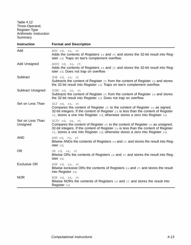
Table 4.12Three-Operand,Register-TypeArithmetic InstructionSummary
Instruction Format and Description
Add ADD rd, rs, rtAdds the contents of Registers rs and rt and stores the 32-bit result into Reg-ister rd . Traps on two’s complement overflow.
Add Unsigned ADDU rd, rs, rtAdds the contents of Registers rs and rt and stores the 32-bit result into Reg-ister rd . Does not trap on overflow.
Subtract SUB rd, rs, rtSubtracts the content of Register rt from the content of Register rs and storesthe 32-bit result into Register rd . Traps on two’s complement overflow.
Subtract Unsigned SUBU rd, rs, rtSubtracts the content of Register rt from the content of Register rs and storesthe 32-bit result into Register rd . Does not trap on overflow.
Set on Less Than SLT rd, rs, rtCompares the content of Register rt to the content of Register rs as signed,32-bit integers. If the content of Register rs is less than the content of Registerrt , stores a one into Register rd ; otherwise stores a zero into Register rd .
Set on Less ThanUnsigned
SLTU rd, rs, rtCompares the content of Register rt to the content of Register rs as unsigned,32-bit integers. If the content of Register rs is less than the content of Registerrt , stores a one into Register rd ; otherwise stores a zero into Register rd .
AND AND rd, rs, rtBitwise ANDs the contents of Registers rs and rt and stores the result into Reg-ister rd .
OR OR rd, rs, rtBitwise ORs the contents of Registers rs and rt and stores the result into Reg-ister rd .
Exclusive OR XOR rd, rs, rtBitwise exclusive ORs the contents of Registers rs and rt and stores the resultinto Register rd .
NOR NOR rd, rs, rtBitwise NORs the contents of Registers rs and rt and stores the result intoRegister rd .

4-14 Instructions
4.6Jump andBranchInstructions
Jump and Branch Instructions change the control flow of a program. AllJump and Branch Instructions occur with a one-instruction delay. That is,the instruction immediately following the jump or branch is always exe-cuted while the target instruction is being fetched from storage. Refer toSection 2.5, “Branch Delay Slot,” for a detailed discussion of the DelayedJump and Branch Instructions.
The J-type instruction format is used for both jump and jump-and-linkinstructions for subroutine calls. In this format, the 26-bit target addressis shifted left two bits and combined with the 4 high-order bits of thecurrent program counter to create a 32-bit absolute address.
The R-type instruction format, which takes a 32-bit byte addresscontained in a register, is used for returns, dispatches, and cross-pagejumps.
Table 4.13Shift InstructionSummary
Instruction Format and Description
Shift Left Logical SLL rd, rt, shamtShifts the bits of Register rt left by shamt bits, and inserts zeros into the low-order bits. Stores the 32-bit result into Register rd.
Shift Right Logical SRL rd, rt, shamtShifts the bits of Register rt right by shamt bits, and inserts zeros into the high-order bits. Stores the 32-bit result into Register rd .
Shift Right Arithmetic SRA, rd, rt, shamtShifts the bits of Register rt right by shamt bits, and sign-extends the high-orderbits. Stores the 32-bit result into Register rd .
Shift Left LogicalVariable
SLLV rd, rt, rsShifts the bits of Register rt left by the value contained in the low-order 5 bitsof Register rs . Inserts zeros into the low-order bits of Register rt and stores the32-bit result into Register rd .
Shift Right LogicalVariable
SRLV rd, rt, rsShifts the bits of Register rt right by the value contained in the low-order 5 bitsof Register rs . Inserts zeros into the high-order bits of Register rt and storesthe 32-bit result into Register rd .
Shift Right ArithmeticVariable
SRAV rd, rt, rsShifts the bits of Register rt right by the value contained in the low-order 5 bitsof Register rs . Sign-extends the high-order bits of Register rt and stores the32-bit result into Register rd.

Jump and Branch Instructions 4-15
Branches have 16-bit signed offsets relative to the program counter(I-type). Jump-and-link and Branch-and-link Instructions save a returnaddress in Register 31.
Table 4.14 summarizes the CW400x Jump and Branch Instructions.
Table 4.14Jump and BranchInstruction Summary
Instruction Format and Description
Jump J targetShifts the 26-bit target address left two bits, combines this value with the fourhigh-order bits of the program counter, and jumps to the address with a one-instruction delay.
Jump and Link JAL targetShifts the 26-bit target address left two bits, combines this value with the fourhigh-order bits of the program counter, and jumps to the address with a one-instruction delay. Stores the address of the instruction following the delay slotinto Register r31 (the Link Register).
Jump Register JR rsJumps to the address contained in Register rs with a one-instruction delay.
Jump and LinkRegister
JALR rs, rdJumps to the address contained in Register rs with a one-instruction delay.Stores the address of the instruction following the delay slot into Register rd .
Branch on Equal BEQ rs, rt, offsetBranches to the target address1 if the content of Register rs is equal to the con-tents of Register rt .
Branch on Not Equal BNE rs, rt, offsetBranches to the target address if the content of Register rs does not equal thecontents of Register rt .
Branch on Less Thanor Equal to Zero
BLEZ rs, offsetBranches to the target address if the content of Register rs is less than or equalto zero.
Branch on GreaterThan Zero
BGTZ rs, offsetBranches to the target address if the content of Register rs is greater than zero.
Branch on Less ThanZero
BLTZ rs, offsetBranches to the target address if the content of Register rs is less than zero.
Branch on Less Thanor Equal to Zero
BGEZ rs, offsetBranches to the target address if the content of Register rs is greater than orequal to zero.
(Sheet 1 of 2)

4-16 Instructions
4.7Branch LikelyInstructions
Branch Likely Instructions change the control flow of a program. AllBranch Likely Instructions occur with a one-instruction delay (the instruc-tion immediately following the branch is normally executed while thetarget instruction is being fetched from storage). However, if the condi-tional branch is not taken, the instruction in the branch delay slot isnullified.
Refer to Section 2.5, “Branch Delay Slot,” for a detailed discussion of thedelayed branch instructions.
Branches have 16-bit signed offsets relative to the program counter(I-type). Branch-and-link Instructions save a return address in Register31.
Branch on Less ThanZero and Link
BLTZAL rs, offsetStores the address of the instruction following the delay slot into Register r31(the Link Register). Branches to the target address if Register rs is less thanzero.
Branch on Less Thanor Equal to Zero andLink
BGEZAL rs, offsetStores the address of the instruction following the delay slot into Register r31(the Link Register). Branches to the target address if Register rs is greater thanor equal to zero.
Branch onCoprocessor z True
BCzT offsetComputes a branch target address by adding the address of the instruction tothe 16-bit offset (shifted left two bits and sign-extended to 32 bits). Branchesto the target address (with a delay of one instruction) if Coprocessor z’s condi-tion line (BCPCONDPz signal) is true.
Branch onCoprocessor z False
BCzF offsetComputes a branch target address by adding the address of the instruction tothe 16-bit offset (shifted left two bits and sign-extended to 32 bits). Branchesto the target address (with a delay of one instruction) if Coprocessor z’s condi-tion line (BCPCONDPz signal) is false.
1. All Branch Instruction target addresses are computed as follows: add the address of the instructionin the delay slot and the 16-bit offset (shifted left two bits and sign-extended to 32 bits). All branchesoccur with a delay of one instruction.
Table 4.14 (Cont.)Jump and BranchInstruction Summary
Instruction Format and Description
(Sheet 2 of 2)

Branch Likely Instructions 4-17
Table 4.15 summarizes the CW400x Branch Likely Instructions. Theseinstructions are MIPS-II Instructions.
Table 4.15Branch LikelyInstruction Summary
Instruction Format and Description
Branch on EqualLikely
BEQL rs, rt, offsetBranches to the target address1 if the contents of Register rs is equal to thecontents of Register rt . If the conditional branch is not taken, the instruction inthe branch delay slot is nullified.
Branch on Not EqualLikely
BNEL rs, rt, offsetBranches to the target address if the contents of Register rs does not equal thecontents of Register rt . If the conditional branch is not taken, the instruction inthe branch delay slot is nullified.
Branch on Less Thanor Equal to ZeroLikely
BLEZL rs, offsetBranches to the target address if the contents of Register rs is less than orequal to zero. If the conditional branch is not taken, the instruction in the branchdelay slot is nullified.
Branch on GreaterThan Zero Likely
BGTZL rs, offsetBranches to the target address if the contents of Register rs is greater than zero.If the conditional branch is not taken, the instruction in the branch delay slot isnullified.
Branch on Less ThanZero Likely
BLTZL rs, offsetBranches to the target address if the contents of Register rs is less than zero.If the conditional branch is not taken, the instruction in the branch delay slot isnullified.
Branch on Less Thanor Equal to ZeroLikely
BGEZL rs, offsetBranches to the target address if the contents of Register rs is greater than orequal to zero. If the conditional branch is not taken, the instruction in the branchdelay slot is nullified.
Branch on Less ThanZero and Link Likely
BLTZALL rs, offsetStores the address of the instruction following the delay slot into Register r31(the Link Register). Branches to the target address if the contents of Register rsis less than zero. If the conditional branch is not taken, the instruction in thebranch delay slot is nullified.
Branch on Less Thanor Equal to Zero andLink Likely
BGEZALL rs, offsetStores the address of the instruction following the delay slot into Register r31(the Link Register). Branches to the target address if the contents of Register rsis greater than or equal to zero. If the conditional branch is not taken, the instruc-tion in the branch delay slot is nullified.
(Sheet 1 of 2)

4-18 Instructions
4.8Special ControlInstructions
Special Control Instructions cause an unconditional branch to thegeneral exception-handling vector. Special Control Instructions arealways R-type. Table 4.16 summarizes these instructions. These instruc-tions are MIPS-II Instructions.
Branch onCoprocessor z TrueLikely
BCzTL offsetComputes a branch target address by adding the address of the instruction tothe 16-bit offset (shifted left two bits and sign-extended to 32 bits). Branchesto the target address (with a delay of one instruction) if Coprocessor z’s condi-tion line (BCPCONDPz signal) is true. If the conditional branch is not taken, theinstruction in the branch delay slot is nullified.
Branch onCoprocessor z FalseLikely
BCzFL offsetComputes a branch target address by adding the address of the instruction tothe 16-bit offset (shifted left two bits and sign-extended to 32 bits). Branchesto the target address (with a delay of one instruction) if Coprocessor z’s condi-tion line (BCPCONDPz signal) is false. If the conditional branch is not taken, theinstruction in the branch delay slot is nullified.
1. All branch instruction target addresses are computed as follows: add the address of the instructionin the delay slot and the 16-bit offset (shifted left two bits and sign-extended to 32 bits). All branchesoccur with a delay of one instruction.
Table 4.15 (Cont.)Branch LikelyInstruction Summary
Instruction Format and Description
(Sheet 2 of 2)
Table 4.16Special ControlInstruction Summary
Instruction Format and Description
System Call SYSCALLInitiates a system call trap and immediately transfers control to the ExceptionHandler.
Breakpoint BREAKInitiates a breakpoint trap and immediately transfers control to the ExceptionHandler.

Trap Instructions 4-19
4.9TrapInstructions
Trap Instructions cause the CW400x to trap to the Exception Handler, ifcertain test conditions are true. Table 4.17 summarizes the CW400x TrapInstructions.
Table 4.17Trap InstructionSummary
Instruction Format and Description
Trap on Equal TEQ rs, rtCompares content of Registers rs and rt . Traps if the content of Register rs isequal to the content of Register rt .
Trap on EqualImmediate
TEQI rs, immediateCompares the 16-bit, sign-extended immediate with the content of Register rsas signed 32-bit integers. Traps if the content of Register rs is equal to the sign-extended immediate .
Trap on Greater Thanor Equal
TGE rs, rtCompares the contents of Registers rs and rt as signed integers. Traps if thecontent of Register rs is greater than or equal to the content of Register rt .
Trap on Greater Thanor Equal Immediate
TGEI rs, immediateCompares the 16-bit, sign-extended immediate with the content of Register rsas signed 32-bit integers. Traps if the content of Register rs is greater than orequal to the sign-extended immediate .
Trap on Greater Thanor Equal ImmediateUnsigned
TGEIU rs, immediateCompares the 16-bit, sign-extended immediate with Register rs as unsigned32-bit integers. Traps if the content of Register rs is less than the sign-extendedimmediate .
Trap on Greater Thanor Equal Unsigned
TGEU rs, rtCompares the contents of Registers rs and rt as unsigned integers. Traps if thecontent of Register rs is greater than or equal to the content of Register rt .
Trap on Less Than TLT rs, rtCompares the contents of Registers rs and rt as signed integers. Traps if thecontent of Register rs is less than the content of Register rt .
Trap on Less ThanImmediate
TLTI rs, immediateCompares the 16-bit, sign-extended immediate with the content of Register rsas signed 32-bit integers. Traps if the content of Register rs is less than the sign-extended immediate .
Trap on Less ThanImmediate Unsigned
TLTIU rs, immediateCompares the 16-bit, sign-extended immediate with the content of Register rsas unsigned 32-bit integers. Traps if the content of Register rs is less than thesign-extended immediate .
Trap on Less ThanUnsigned
TLTU rs, rtCompares the content of Registers rs and rt as unsigned integers. Traps if thecontent of Register rs is less than the content of Register rt .

4-20 Instructions
4.10CoprocessorInstructions
For Coprocessor 3 to 1 Instructions, users need to make sure that thecorresponding Coprocessor Usable Bits, Cu[3:1], in the Status Registerare set. If the coprocessors are not enabled, the corresponding copro-cessor instructions will cause a Coprocessor Unusable (CpU) Exception.This also applies to Coprocessor 0, except if the processor is in KernelMode, the Cu0 Bit does not matter. Also note that the LWC0 and SWC0will cause an RI Exception.
Coprocessor Branch Instructions are J-type. Table 4.18 summarizes thedifferent Coprocessor Instructions.
Table 4.18Coprocessor InstructionSummary
Instruction Format and Description
Load Word toCoprocessor
LWCz rt, offset(base)Sign-extends the 16-bit offset and adds this value to the content of Registerbase to create an address. Loads the content of addressed word into Registerrt of Coprocessor z.
Store Word fromCoprocessor
SWCz rt, offset(base)Sign-extends the 16-bit offset and adds this value the to the content of Registerbase to create an address. Stores the content of Register rt from Coprocessorz to the addressed word.
Move to Coprocessor MTCz rt, rdMoves content of CW400x Register rt into Register rd of Coprocessor z.
Move fromCoprocessor
MFCz rt, rdMoves the content of Register rd of Coprocessor z into CW400x Register rt .
Move Control toCoprocessor
CTCz rt, rdMoves the content of CW400x Register rt into Control Register rd of Coproces-sor z.
Move Control fromCoprocessor
CFCz rt, rdMoves the content of Control Register rd of Coprocessor z into CW400x Reg-ister rt .
CoprocessorOperation
COPz cofunCoprocessor z performs the user defined coprocessor function cofun . TheCW400x’s state is not modified.
Branch onCoprocessor z True
BCzT offsetComputes a branch target address by adding the address of the instruction tothe 16-bit offset (shifted left two bits and sign-extended to 32 bits). Branchesto the target address (with a delay of one instruction) if coprocessor z’s conditionline (BCP_CONDPz signal) is true.
(Sheet 1 of 2)

System Control Coprocessor (CP0) Instructions 4-21
4.11System ControlCoprocessor(CP0)Instructions
Coprocessor 0 Instructions perform operations on the System ControlCoprocessor (CP0) Registers to manipulate the memory managementand exception-handling facilities of the processor. Table 4.19 summarizesthe CP0 Instructions.
The CW400x and the MR400x treat TLB Access Instructions as NOPs.
When in User Mode, if the Cu0 Bit in the Status Register is set to zero,the CW400x takes a Coprocessor Unusable Exception if it decodes aRFE, MTC0, or MFC0 Instruction.
Branch onCoprocessor z False
BCzF offsetComputes a branch target address by adding the address of the instruction tothe 16-bit offset (shifted left two bits and sign-extended to 32 bits). Branchesto the target address (with a delay of one instruction) if coprocessor z’s conditionline (BCPCONDPz signal) is false.
Branch onCoprocessor z TrueLikely
BCzTL offsetSee Table 4.15, “Branch Likely Instruction Summary.”
Branch onCoprocessor z FalseLikely
BCzFL offsetSee Table 4.15, “Branch Likely Instruction Summary.”
Table 4.18 (Cont.)Coprocessor InstructionSummary
Instruction Format and Description
(Sheet 2 of 2)
Table 4.19CP0 InstructionSummary
Instruction Format and Description
Move to CP0 MTC0 rt, rdLoads the content of the CW400x rt into the CP0 Register rd .
Move from CP0 MFC0 rt, rdLoads the content of the CP0 Register rd into the CW400x rt .
Restore fromException
RFERestores the previous interrupt mask and mode bits of the Status Register intothe current status bits. Restores the old status bits into the previous status bits.
Wait for Interrupt WAITIStops execution of instructions and places the processor into a power save con-dition until a hardware interrupt or reset is received.

4-22 Instructions
Figure 4.5 shows the waveforms for the WAITI Instruction.
Figure 4.5WAITI InstructionWaveforms
The opcode encoding for the WAITI Instruction is shown in Tables 4.2and 4.7.
BINTP0
CRUN_INN
CWAITIP
WAITI - X1
ADDRP[31:0]
WAITI - IF WAITI - WB
PCLK
CRUN_OUTP
Exception Vector

5-1
Chapter 5Exception Processing(CP0)
This chapter describes exception processing in the MiniRISC CW400xMicroprocessor Core. The System Control Coprocessor (CP0) processesexceptions.
This chapter contains the following sections:
♦ Section 5.1, “Exception Handling Registers”
♦ Section 5.2, “Exception Processing”
♦ Section 5.3, “Exception Description Details”
5.1ExceptionHandlingRegisters
Table 5.1 shows the registers that the CW400x uses to handle excep-tions. During exception processing, software can examine these registersto determine the cause of an exception and the state of the CW400x.
The Translation Lookaside Buffer (TLB) Registers (EntryHi, EntryLo,Index, Random, BadVA, and Context) are used only when an MMU isattached to the CW400x. These registers are not implemented as part ofthe basic CW400x Microprocessor Core. However, the CW400x CBusInterface does include hooks to attach a TLB as an external part ofCoprocessor 0. The user accesses the TLB Registers as if they were inthe CW400x. The CW400x maps these accesses to the registers in theMMU.
The CW400x registers are described in detail in the following subsec-tions. The TLB Registers are described in detail in the MiniRISC BuildingBlocks Technical Manual.

5-2 Exception Processing (CP0)
Table 5.1Exception-ProcessingRegisterAddresses
5.1.1Status Register(R12)
The format of the CW400x Status Register is similar to the R3000 StatusRegister, except the CW400x Status Register does not contain the PE(Parity Error), CM (Cache Miss), PZ (Parity Zero), SwC (Swap Caches),or the IsC (Isolate Cache) Bits (Bits 16-20). These fields are definedunusable (value: 0). However, the functionality of the register and theremaining fields is the same as the R3000.
The Status Register contains all major status bits for exception condi-tions. All defined bits in the Status Register, with the exception of the TS(TLB Shutdown) Bit, are readable and writable; the TS Bit is read-only.Additional details on the function of each Status Register bit are providedin the paragraphs that follow.
Figure 5.1 shows the format of the Status Register. Upon reset, BEV =1, and KUc = 0, and IEc = 0; all other bits of this register are undefined.
RegisterAddress Register Name
0 Index1
1. Used only when an MMU is attached, and isdescribed in the MiniRISC Building BlocksTechnical Manual.
1 Random1
2 EntryLo1
4 Context1
8 Bad Virtual Address1
10 EntryHi1
12 Status
13 Cause
14 Exception Program Counter
15 Processor Revision Identifier

Exception Handling Registers 5-3
Figure 5.1Status Register
Cu[3:0] Coprocessor Usability Bits [31:28]Software sets the corresponding bits of Cu[3:0] to one toindicate that the associated coprocessor is usable. Bit 31corresponds to Coprocessor 3 and Bit 28 corresponds toCoprocessor 0. When a coprocessor instruction refer-ences a disabled coprocessor, it causes a CoprocessorUnusable Exception (CpU). Note that the System ControlCoprocessor (CP0) is always considered usable whenthe CW400x is operating in kernel mode, regardless ofthe setting of the Cu0 Bit.
R Reserved [ 27:23], [20:16], [7:6]These bits are reserved and read as zero. The CW400xignores attempts to set these bits; however, softwareshould write these bits as zero to ensure compatibilitywith future versions of hardware.
BEV Bootstrap Exception Vector 22This bit selects between two destination addresses forexceptions.
The BEV Bit controls the location of Exception Vectorsduring bootstrap (immediately following reset). When thisbit is set to zero, the Normal Exception Vector locationsare used; when the bit is set to one, Bootstrap ExceptionVector locations are used.
BEV set to Zero – The UTLB Miss Exception Vector islocated at 0x80000000, and the General Exception Vec-tor is located at 0x80000080.
BEV set to One – The UTLB Miss Exception Vector isrelocated to an address of 0xBFC00100, and the GeneralException Vector is relocated to 0xBFC00180. This alter-nate set of vectors can be used when diagnostic testscause exceptions to occur prior to verification of properoperation of the cache and main memory system.
The CW400x sets this bit to one upon deassertion of theReset Signal.
31 28 27 23 22 21 20 16 15 10 9 8 7 6 5 4 3 2 1 0
Cu[3:0] R BEV TS R Intr[5:0] Sw[1:0] R KUo IEo KUp IEp KUc IEc

5-4 Exception Processing (CP0)
TS TLB Shutdown 21This bit indicates that the TLB has shut down due to anattempt to access several TLB entries at the same time.This bit is read-only.
Intr[5:0] Hardware Interrupt Enables Mask [15:10]Software sets these six bits to one to enable the corre-sponding hardware interrupts. Bit 15 corresponds toINT5, and Bit 10 corresponds to INT0. All interrupts canbe disabled by clearing the Interrupt Enable Bit (IEc)described below.
Sw[1:0] Software Interrupt Enables Mask [9:8]Software sets these two bits to one to enable the corre-sponding software interrupts. All interrupts can be dis-abled by clearing the Interrupt Enable Bit (IEc) describedbelow.
KUo, p, c Kernel/User Mode, Old/Previous/Current 5, 3, 1The KUo, KUp, and KUc bits comprise a three-level stackshowing the old/previous/current mode (zero means ker-nel; one means user). The occurrence of an exceptionautomatically puts the system in Kernel Mode. Manipula-tion and use of these bits during exception processing isdescribed in Section 5.2.2, “Status Register Mode Bitsand Exception Processing.”
IEo, p, c Interrupt Enable, Old/Previous/Current 4, 2, 0The IEo, IEp, and IEc Bits comprise a 3-level stack show-ing the old/previous/current interrupt enable settings(zero means disabled; one means enabled). Manipulationand use of these bits during exception processing isdescribed in Section 5.2.2, “Status Register Mode Bitsand Exception Processing.”
5.1.2Cause Register(R13)
The format of the Cause Register is the same in the CW400x as in theR3000. The only difference is the way the CW400x sets the BD (BranchDelay) Bit. The CW400x sets the BD Bit only when an exception occursduring the execution of the instruction in the branch delay slot and thebranch is taken. If the branch is not taken then the CW400x will not setthe BD Bit, even if an exception occurs during the delay slot.
The contents of the Cause Register describe the last occurring excep-tion. A four-bit exception code (ExcCode) indicates the cause of the

Exception Handling Registers 5-5
exception. The remaining bit fields contain detailed information specificto certain exceptions. With the exception of the SI[1:0] Bits, all bits in theregister are read-only. Writes to the SI[1:0] Bits set or reset softwareinterrupts. The description also lists and briefly describes all possibleexception causes. All bits in this register are undefined on reset.
Figure 5.2 shows the format of the Cause Register. Upon reset, the con-tent of this register is undefined.
Figure 5.2Cause Register
BD Branch Delay 31The CW400x sets this bit to one to indicate that the lastexception was taken while executing in a branch delayslot and the branch was taken. (Differs from the R3000and 4000)
R Reserved 30, [27:16], [7:6], [1:0]These bits are reserved and read as zero. The CW400xignores attempts to set these bits; however, softwareshould write these bits as zero to ensure compatibilitywith future versions of hardware.
CE Coprocessor Error [29:28]When taking a Coprocessor Unusable Exception, theCW400x writes the referenced coprocessor number inthis field. This field is otherwise undefined.
IP[5:0] Interrupt Pending [15:10]The CW400x sets these bits to indicate that an externalinterrupt is pending. Bit 15 corresponds to Interrupt 5 andBit 10 corresponds to Interrupt 0. For MIPS compatibility,the Interrupt Pending Bits should be attached to Copro-cessors as follows:
31 30 29 28 27 16 15 10 9 8 7 6 5 2 1 0
BD R CE Reserved IP[5:0] SI[1:0] R ExcCode R

5-6 Exception Processing (CP0)
The system designer can attach Interrupts 0 and 1 anyway he wants.
SI[1:0] Software Interrupts [9:8]By setting either of these bits to one, software causes theCW400x to transfer control to the general exceptionroutine. The exception routine can tell which softwareinterrupt bit is set (pending) by reading this field. Theexception routine must reset the SI[1:0] Bits to zerobefore returning control to the interrupting software.
ExcCode Exception Code [5:2]The CW400x sets this field to indicate the type of eventthat caused the last general exception. The four bits areencoded as described in the table below. For more detailsee Table 5.2.
15 1011121314
Coprocessor 0, Interrupt 2
Coprocessor 1, Interrupt 3, FPU
Coprocessor 2, Interrupt 4
Coprocessor 3, Interrupt 5
[5:2] Mnemonic Description
0x0 Int Interrupt
0x1 TLBMOD TLB Modification Exception
0x2 TLBL TLB Miss Exception, Load or Instruction
0x3 TLBS TLB Miss Exception, Store
0x4 AdEL Address Error Exception, Load or Instruction
0x5 AdES Address Error Exception, Store
0x6 IBE Bus Error Exception, Instruction Fetch
0x7 DBE Bus Error Exception, Data Load or Store
0x8 Sys System Call Exception (SYSCALL Instr.)
0x9 Bp Breakpoint Exception
0xA RI Reserved Instruction Exception
0xB CpU Coprocessor Unusable Exception
0xC Ovf Arithmetic Overflow Exception
0xD Tr Trap Exception
0xE Reserved
0xF Reserved

Exception Handling Registers 5-7
5.1.3ExceptionProgramCounter (EPC)Register (R14)
The 32-bit, read-only Exception Program Counter (EPC) Registercontains the address of the instruction that caused the exception.However, when the exception instruction resides in a branch delay slotand the branch is taken, the CW400x sets the Cause Register BD Bitand places the address of the immediately preceding branch or jumpinstruction into the EPC Register.
The EPC Register behaves like the R3000 EPC Register except whenan exception occurs in the branch delay slot and the branch is not taken.In this case, the EPC Register points to the instruction causing theexception, even if it is in the delay slot. The R3000 EPC Register alwaysreflects the branch instruction address when the delay slot contains theexception-causing instruction, no matter if the branch was taken or not.
Figure 5.3 shows the format of the EPC Register. Upon reset, the contentof this register is undefined.
Figure 5.3EPC Register
EPC Virtual Address [31:0]This register contains the Virtual Address of the excep-tion-causing instruction or the address of the immediatelypreceding branch or jump instruction.
5.1.4ProcessorRevisionIdentifier (PRId)Register (R15)
This register contains information that identifies the implementation andrevision level of the processor. The format is the same as the R3000. Itshould be noted that the user should not depend on this field to identifythe revision of any MiniRISC microprocessor.
The PRId Register is read-only. The lowest four bits of each field areinputs into the CW400x (CLOIDP[3:0] and CLOPRP[3:0]) and arehardwired to a defined value.
The Processor Revision Identifier (PRId) Register contains informationthat identifies the implementation and revision level of the processor andsystem control coprocessor.
31 0
EPC

5-8 Exception Processing (CP0)
The revision number distinguishes some chip revisions. However, LSILogic is free to change this register at any time and does not guaranteethat changes to its chips will necessarily change the revision number orthat changes to the revision number necessarily reflect real chipchanges. For this reason, software should not rely on the revisionnumber to characterize the chip.
Figure 5.4 shows the format of the PRId Register. Upon reset, thecontent of this register is 0x00001000.
Figure 5.4PRId Register
R Reserved [31:16]These bits are reserved and read as zero. The CW400xignores attempts to set these bits.
IMP Implementation [15:8]This eight-bit field contains the CW400x’s implementationnumber. Bits [15:12] are hardwired to 00012. TheCLOIDP[3:0] inputs drive Bits [11:8].
REV Revision [7:0]This eight-bit field contains the CW400x’s revisionnumber. Bits [7:4] are hardwired to 00002. TheCLOPRP[3:0] inputs drive Bits [3:0].
31 16 15 8 7 0
R IMP REV

Exception Processing 5-9
5.2ExceptionProcessing
Table 5.2 lists and describes CW400x supported exceptions.
Table 5.2CW400xExceptions
When an exception occurs, the CW400x aborts the current instructionand all instructions following in the pipeline that have already begunexecution. The exception puts the system in kernel mode. The CW400xsets the ExcCode in the Cause Register (see Section 5.1.2, “Cause Reg-ister (R13)”). The CW400x jumps directly into a designated exceptionhandler routine. The CW400x loads the Exception Program Counter(EPC) Register with an appropriate restart location where execution mayresume after the exception is serviced. The restart location in the EPCis the address of the instruction that caused the exception or, if theinstruction was executing in a branch delay slot and the branch is taken,
Exception Description
Reset Assertion of the Reset Signal causes an exception thattransfers control to the Special Vector at virtual address0xBFC00000.
User TLB Miss A reference is made to a page in kuseg that has nomatching TLB entry.
TLB Miss A referenced TLB entry’s Valid Bit is not set or a referenceis made to the kseg2 page that has no matching TLB Entry.
TLB Modified During a store, the valid bit is set but the Dirty Bit is not setin the referenced TLB Entry.
Bus Error Assertion of the Bus Error Signal.
Address Error Attempt to load, fetch, or store an unaligned word, or refer-ence to a virtual address with the most significant bit setwhile in User Mode.
Overflow Two’s complement overflow during add or subtract.
System Call Execution of the SYSCALL Instruction.
Breakpoint Execution of the BREAK Instruction.
ReservedInstruction
Execution of an instruction with undefined opcode fields.
CoprocessorUnusable
Execution of a coprocessor instruction when theappropriate Cu Bit is not set.
Interrupt Assertion of one of the six hardware interrupt inputs orsetting one of the two software interrupt bits in the CauseRegister.
Trap Execution of a Trap Instruction with a true condition.

5-10 Exception Processing (CP0)
the address of the branch instruction immediately preceding the delayslot. Even though the processor is pipelined, exceptions are reported inthe order they occur, so all exceptions for the current instruction arereported prior to exceptions for successive instructions. The characteris-tics of the machine’s pipeline staging, however, cannot guarantee that allprocessor and associated system states will remain completelyunchanged as a result of the (possibly incomplete) execution of theinstruction immediately following an instruction that causes an exception.Examples of these state changes include:
♦ Instructions may have been read from memory and loaded into theI-Cache.
♦ The cache may have been updated in response to a bus error on acacheable, memory write operation.
The above events can normally be ignored because enough of themachine’s state is restored so that execution always resumes properlyafter servicing the exception.
This subsection describes the CW400x’s exception handlingmechanisms, the System Control Coprocessor (CP0) Registers, and allevents that cause exceptions.
The CW400x is always in one of two operating modes: normal or excep-tion. In the normal operating mode, the CW400x executes the program-specified sequence of instructions. In the exception mode, the normalsequence of instruction execution is suspended to allow the CW400x torespond to abnormal or asynchronous events. The CW400x’s exception-handling system efficiently manages machine exceptions, including arith-metic overflows, I/O interrupts, and system calls.
Exception causes are the same for the CW400x and the R4000, but theCW400x implements the Exception Registers differently than the R4000.The CW400x has all the same registers as the R4000 but not all thesame register fields.
The only functional difference in exception handling is the implementationof the BD Bit in the Cause Register and the behavior of the EPC Regis-ter. The CW400x sets the BD Bit only if the branch is taken and anexception occurs in the delay slot. The EPC Register will then containthe address of the branch, not the exception-causing instruction’s

Exception Processing 5-11
address. Otherwise, the CW400x does not set the BD Bit and the EPCRegister contains the address of the exception-causing instruction.
Each MiniRISC exception - its cause, handling and servicing is identicalto the R4000, with the special case of an exception occurring in thebranch delay slot (see Section 2.5, “Branch Delay Slot”).
Each exception is classified into the stage where the exception isacknowledged. For all IF Exceptions, the Instruction Fetch is invalidatedand in the next run cycle (a clock cycle in which the CW400x is running)the exception is taken. For X1 and X2 Exceptions, the CW400x takes theexception in the same cycle the exception is signaled (the InternalException Taken Signal is asserted). For WB Exceptions, the CW400xtakes the exception in the next run cycle.
5.2.1ExceptionVectorLocations
Table 5.3 shows the three different addresses the CW400x uses forexception vectors.
If the BEV (Bootstrap Exception Vector) Bit in the Status Register is setto one, the UTLB Miss Exception Vector address is changed to0xBFC00100, and the General Exception Vector is changed to0xBFC00180 while the Reset Vector remains unchanged.
Table 5.3Exception VectorLocations
5.2.2Status RegisterMode Bits andExceptionProcessing
When the CW400x responds to an exception, it saves the current Ker-nel/User Mode (KUc) and current Interrupt Enable Mode (IEc) Bits of theStatus Register into the previous Mode Bits (KUp and IEp). It saves theprevious Mode Bits (KUp and IEp) into the old Mode Bits (KUo and IEo).It clears the current mode bits (KUc and IEc) to cause the processor toenter the kernel operating mode and to disable all interrupts.
This three-level set of mode bits lets the CW400x respond to two levelsof exceptions before software must save the contents of the StatusRegister. Figure 5.5 shows how the CW400x manipulates the StatusRegister during exception recognition.
Exception VectorNormalLocation
BootstrapLocation
Reset 0xBFC00000 0xBFC00000
UTLB Miss 0x80000000 0xBFC00100
General 0x80000080 0xBFC00180

5-12 Exception Processing (CP0)
Figure 5.5Status RegisterChanges DuringExceptionRecognition
After an exception handler has completed execution, the CW400x mustreturn to the system context that existed prior to the exception (if possi-ble). The Restore From Exception (RFE) Instruction provides the mech-anism for this return.
The RFE Instruction restores control to a process that was preempted byan exception. When the RFE instruction is executed, it restores the pre-vious Interrupt Mask (IEp) Bit and Kernel/User Mode (KUp) Bit in the Sta-tus Register into the corresponding current Status Bits (IEc and KUc). Italso restores the old Status Bits (IEo and KUo) into the correspondingprevious status bits (IEp and KUp). The old status bits (IEo and KUo)remain unchanged. Figure 5.6 illustrates the actions of the RFEInstruction.
Figure 5.6Restoring Controlfrom Exceptions(RFE Instruction)
5.2.3System ControlCoprocessor(CP0) Function
The CP0 generates the Kill Signals needed by the CW400x and periph-erals for instruction cancellation in the case of exceptions. The CP0 pro-cesses the exceptions detected by the CW400x and peripherals byupdating the Exception Handling Registers to reflect the state of theexception. The CP0 contains the four registers that are important inexception processing: the Status Register, the Cause Register, the EPCRegister, and the Processor Revision Identification Register. After reset,
6 5 4 3 2 1 0
IEo KUp IEp KUc IEcKUo
IEo KUp IEp KUc IEcKUo
0 0
StatusRegister
StatusRegister
ExceptionRecognition
6 5 4 3 2 1 0
IEo KUp IEp KUc IEcKUo
IEo KUp IEp KUc IEcKUo
Status
Return FromException
Register
StatusRegister

Exception Processing 5-13
in the Reset Exception Handler, the software should initialize these reg-isters since most of the fields come up undefined.
5.2.4RegisterAccesses
The only way to access the CP0 Registers is by using the Move Fromand To Coprocessor Zero Instructions, MFC0 and MTC0. Table 5.4shows the register numbers for the CP0 registers.
Table 5.4CP0 RegisterAddresses
The transaction protocols initiated by these commands do not resemblethe MFC/MTCs for external coprocessors, because the CP0 is not anexternal coprocessor. The CP0 is integrated into the CW400x, allowingdirect access to the internal data flow.
5.2.5ExceptionHandling
The conditions that cause the instruction flow to deviate from the normalflow of execution are called exceptions. If two exceptions occur simulta-neously, the one with the higher priority takes precedence and is ser-viced. The Cause and the EPC Registers will reflect the exception withthe higher priority. Table 5.5 lists the specific exception conditions in hier-archical order from highest to lowest priority.
Exceptions cause the CW400x to update the Status, Cause, and EPCRegisters and jump instruction flow to an Exception Vector. The CW400xalso generates the appropriate Kill (Instruction Invalidate) Signals,CKILLMEMP, CKILLXP, and CKILLWP. CKILLMEMP is used to kill exter-nal memory transactions, CKILLXP is used to kill the instruction in theExecute (X) Stage, and CKILLWP is used to kill the instruction in theWriteback Stage.
RegisterNumber Register Name
R12 Status
R13 Cause
R14 Exception Program Counter
R15 Processor Revision Identifier

5-14 Exception Processing (CP0)
Table 5.5Exception Priority
Some exceptions have priority over others when simultaneous excep-tions occur. For example, the instruction in the X Stage is the BREAKInstruction, and in the same run cycle an external interrupt is signalled.The BREAK Exception will be serviced before the interrupt, since it is ahigher priority exception.
Figure 5.7 shows typical pipeline flow.
Figure 5.7Typical PipelineFlow
5.2.5.1 Kill (Instruction Invalidate) Signals
Asserting the CKILLXP Signal invalidates the X Stage and Asserting theCKILLWP Signal invalidates the WB Stage. With the exception of inter-rupts and the Branch Likely Instructions, branch not taken, the CW400xasserts CKILLMEMP to kill the current memory transaction (invalidatethe current instruction). The CW400x does not assert CKILLMEMP dur-ing interrupts and Branch Likely Instructions, branch not taken, becauseof possible data dependencies caused by load scheduling. The Kill Sig-nals are only valid on the rising edge of the clock. In the following figures,the Run Signal is sometimes shown to be continuously LOW, which is
Priority ExceptionStageServiced
Reset –
Trap, Overflow, Data Bus Error WB
Data Address Error X2
Data TLB Miss/TLB Miss User X2
TLB Modify X2
Instruction Bus Error X1
SYSCALL/BREAK/TRAP/Reserved Instruction X1
Coprocessor Unusable X1
Interrupt X1
Instruction Address Error IF
Instruction TLB Miss/TLB Miss User IF
Low
est
Hig
hest
IF X1
IF WBX
X1 X2 WB
IF X WB

Exception Processing 5-15
seldom true. When the processor stalls, the CW400x signals areextended until the next run cycle (the Kill Signals are asserted for adefined number of run cycles). Depending on the stall mix, the total num-ber of cycles the signals are asserted will vary with the number of stallcycles.
Figure 5.8 shows the appropriate Kill Signals and their timing in respectto the detection of a Branch Likely Instruction which was not taken, whichoccurs in the X1 Stage.
Figure 5.8Branch Likely,Branch Not Taken(X1 Stage)
5.2.5.2 General Exceptions
Figures 5.9 through 5.11 show examples of the Kill Signals associatedwith exceptions occurring in different stages.
PCLKP
CRUN_INN
CKILLXP
CKILLWP
CKILLMEMP
X1 WBIF (BLTZL)X1 WBIF (Add Instruction Killed)

5-16 Exception Processing (CP0)
Figure 5.9, the waveform for the System Call Exception (SYSCALLInstruction), illustrates how the CW400x behaves in any X1 Stage Excep-tion (shows the instruction invalidate sequence for exceptions during theX1 Stage), except for an Instruction Bus Error (see Figure 5.15). (Seealso Section 5.3.9, “System Call Exception.”)
Figure 5.9X1 StageException (SystemCall)
Figure 5.10, the waveform for the Overflow Exception, is a general wave-form for all exceptions that are signalled in the WB Stage, except for aData Bus Error (see Figure 5.16). (See also Section 5.3.6, “OverflowException.”)
Figure 5.10WB StageException(Overflow)
Figure 5.11 shows the Kill Waveform for an exception signalled in the IFStage. Even though an exception is signalled in the IF Stage, theCW400x does not assert any Kill Signal or Exception Taken Signal until
PCLKP
CRUN_INN
CKILLXP
CKILLWP
X1 WB
CKILLMEMP
EXCEPT_DETECT1
(Internal)
1. EXCEPT_DETECT is an exception detected by the MMU, theALU, a decode, or another external device.
PCLKP
CRUN_INN
CKILLXP
CKILLWP
CKILLMEMP
EXCEPT_DETECT1
(Internal)
1. EXCEPT_DETECT is an exception detected by the MMU, theALU, a decode, or another external device.

Exception Processing 5-17
the following X Stage, except for CKILLMEMP, which is used to kill theInstruction Fetch that causes the exception.
Figure 5.11IF Stage Exception(TLB Miss,Instruction)
Figure 5.12 shows the Kill Waveform for a Reset Exception.The Reset isspecial in that the Kill Signal protocols do not fit into the other threecategories (IF, X, and WB).
Figure 5.12Reset Exception(Special Case)
PCLKP
CRUN_INN
CKILLXP
CKILLWP
IF X1
CKILLMEMP
WB
EXCEPT_DETECT1
(Internal)
1. EXCEPT_DETECT is an exception detected by the MMU, theALU, a decode, or another external device.
PCLKP
CRUN_INN
BCPU_RESETN
CKILLXP
CKILLWP
CKILLMEMP

5-18 Exception Processing (CP0)
Figure 5.13 shows the instruction validation protocol for an exception sig-nalled in the X2 Stage. The Kill Signals, CKILLMEMP and CKILLXP, arevalid on the rising edge at the end of the X2 Stage. These signals areintended to kill the X2 Stage of the exception-causing instruction.
Figure 5.13X2 StageException (TLBMiss, Data Load)
Figure 5.14 shows an interrupt exception signalled in the X2 Stage of aninstruction. The CW400x defers the handling of the interrupt exception tothe next instruction’s Execute Stage, and consequentially the EPC Reg-ister reflects the address of the instruction in the following Execute Stage.Interrupts are never serviced in the X2 Stage. Even when the interrupt isasserted, the exception is not serviced until the following X Stage (X1).
The Interrupt Exception is discussed further in Section 5.2.5.3, “InterruptProcessing.”
Figure 5.14External InterruptSignalled DuringX2 Stage
PCLKP
CRUN_INN
EXCEPT_DETECT1
CKILLXP
CKILLWP
(Internal)
IF X1
CKILLMEMP
X2 WB
1. EXCEPT_DETECT is an exception detected by the MMU, theALU, a decode, or another external device.
X1 X2 WBX2
PCLKP
CRUN_INN
BINTP[5:0]
CKILLXP
CKILLWP
CKILLMEMP

Exception Processing 5-19
There are two exceptions to the general waveforms mentioned in Figures5.13 and 5.14. Bus errors need not be held to the next run cycle in orderto be acknowledged, unlike the other exception signals. So, as long theBus Error Signal is held asserted during the rising edge of the clock, theCW400x will acknowledge it (assuming no higher priority simultaneousexception). Like the IF Exceptions, the CW400x forwards Bus ErrorExceptions into the next stage from when they were asserted (seeFigures 5.15 and 5.16).
Figure 5.15Instruction BusError, (X1 Stage)
Figure 5.16Data Bus Error,(WB Stage)
An interesting case occurs when an IF Exception is signaled and CKILL-MEMP has to be asserted twice. This situation happens when the previ-ous instruction is external memory transaction (LOAD, STORE, MTC,MFC). The CW400x deasserts CKILLMEMP during the memory transac-tions’s X2 Stage to allow the read or write to take place. In the next runcycle, the CW400x asserts the Kill Signals as usual (see Figure 5.17).
PCLKP
CRUN_INN
BBEP
CKILLXP
CKILLWP
IF IF
CKILLMEMP
X1 WB
X2 X2 WB
PCLKP
CRUN_INN
BBEP
CKILLXP
CKILLWP
CKILLMEMP

5-20 Exception Processing (CP0)
Figure 5.17MultipleCKILLMEMPAssertion
5.2.5.3 Interrupt Processing
The CW400x has eight interrupt inputs (six external hardware pins, andtwo software bits in the Cause Register). When the CW400x detects aninterrupt, the CW400x generates an exception and asserts the appropri-ate Kill (Instruction Invalidate) Signals. The CW400x always grants theinterrupt except when the specific interrupt is disabled or when a higherpriority exception occurs simultaneously.
In case of a simultaneous interrupt and a non-interrupt exception, theinterrupt has priority over Instruction Address Error and Instruction TLBMiss. The other exceptions have priority over the interrupt during simul-taneous exception signalling.
Even though an Address Error and an Interrupt can happen simulta-neously, the interrupt has precedence. For interrupts, the CW400xasserts the Kill Signals and asserts the Interrupt Grant Signal, CINTGRP.
FIgures 5.18 and 5.19 show two cases of an external coprocessor, in thiscase a Floating Point Unit, asserting an interrupt. In Figure 5.18 theCW400x does not grant the interrupt, because a simultaneous exception(overflow) occurred in the Writeback Stage of the previous instruction.Since the overflow occurs in a instruction further along in the pipeline, ittakes precedence over the external interrupt and is serviced accordingly.
IF X1 WBX2 WBX1
PCLKP
CRUN_INN
EXCEPT_DETECT1
CKILLXP
CKILLWP
CKILLMEMP
(Exception-Causing(Load or Store)
(Internal)
1. EXCEPT_DETECT is an exception detected by the MMU,the ALU, a decode, or another external device. In this casethe exception is an Instruction TLB Miss.
Instruction)

Exception Processing 5-21
Figure 5.18ExternalCoprocessor (FPU)Interrupt (InterruptNot Taken)
PCLKP
CRUN_INN
CKILLXP
CKILLWP
CKILLMEMP
X WBX WBIF
(Overflow)(Floating Point Interrupt)
CINTGRP
BINTP32
EXCEPT_DETECT1
(Internal)
1. EXCEPT_DETECT is an exception detected by the MMU, theALU, a decode, or another external device. In this case theexception is an Arithmetic Overflow.
2. FPU Interrupt

5-22 Exception Processing (CP0)
In Figure 5.19, two simultaneous exceptions occur: an Address Error inthe IF Stage of a following instruction and an interrupt which occurs inthe X Stage of the instruction. The interrupt takes precedence, since itoccurs in an instruction that is further in the pipeline. The CW400xasserts CINTGRP to acknowledge the interrupt, and the appropriate sig-nals are asserted and values written to the Exception Handling Registersto reflect the taken interrupt. Notice that CKILLMEMP is not asserted forinterrupts. This is the only exception that does not cause CKILLMEMPto be asserted.
Figure 5.19ExternalCoprocessor (FPU)Interrupt (InterruptTaken)
Since interrupts can occur at any time, memory transactions may beerroneously killed. In the case of load scheduling, the load data can beserviced in any stage and is not killed by an interrupt since the loadoccurred many instructions before the interrupt was generated. Interruptsare not acknowledged during an instruction’s X2 Stage to prevent erro-neous memory transaction invalidation (see Figure 5.14.)
Figure 5.20 shows an interrupt being signalled during the Branch LikelyDelay Slot Invalidation Cycle. The CW400x invalidates the instructionafter a Branch Likely, if the branch conditions were not met. The InterruptException will not be serviced until the X Stage of a valid instruction (thenext instruction following the invalidated one in the delay slot).
PCLKP
CRUN_INN
CKILLXP
CKILLWP
CKILLMEMP
CINTGRP
BINTP32
CADDR_ERRORP1
X WBX WBIF
(Floating Point Interrupt)(ADDR_ERR)
1. Address error during an Instruction Fetch.2. FPU Interrupt.
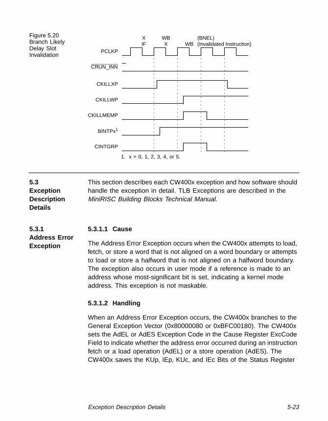
Exception Description Details 5-23
Figure 5.20Branch LikelyDelay SlotInvalidation
5.3ExceptionDescriptionDetails
This section describes each CW400x exception and how software shouldhandle the exception in detail. TLB Exceptions are described in theMiniRISC Building Blocks Technical Manual.
5.3.1Address ErrorException
5.3.1.1 Cause
The Address Error Exception occurs when the CW400x attempts to load,fetch, or store a word that is not aligned on a word boundary or attemptsto load or store a halfword that is not aligned on a halfword boundary.The exception also occurs in user mode if a reference is made to anaddress whose most-significant bit is set, indicating a kernel modeaddress. This exception is not maskable.
5.3.1.2 Handling
When an Address Error Exception occurs, the CW400x branches to theGeneral Exception Vector (0x80000080 or 0xBFC00180). The CW400xsets the AdEL or AdES Exception Code in the Cause Register ExcCodeField to indicate whether the address error occurred during an instructionfetch or a load operation (AdEL) or a store operation (AdES). TheCW400x saves the KUp, IEp, KUc, and IEc Bits of the Status Register
X WBX WBIF
PCLKP
CRUN_INN
CKILLXP
CKILLWP
CKILLMEMP
(BNEL)(Invalidated Instruction)
BINTPx1
CINTGRP
1. x = 0, 1, 2, 3, 4, or 5.

5-24 Exception Processing (CP0)
into the KUo, IEo, KUp, and IEp Bits, respectively, and clears the KUcand IEc Bits.
The EPC Register points to the instruction that caused the exception,unless the instruction is in a branch delay slot and the branch was taken.In that case, the EPC Register points to the branch instruction precedingthe exception-causing instruction and the CW400x sets the BD Bit of theCause Register.
If the system includes an MMU when this exception occurs, the BadVARegister contains the address that was either improperly aligned or thatimproperly addressed kernel data while in user mode.
5.3.1.3 Servicing
Kernel software should indicate a segmentation violation to the executingprocess. Such an error is usually fatal, although an alignment error mightbe handled by simulating the instruction that caused the error.
5.3.2BreakpointException
5.3.2.1 Cause
The Breakpoint Exception occurs when the CW400x executes theBREAK Instruction. This exception is not maskable.
5.3.2.2 Handling
When the Breakpoint Exception occurs, the CW400x branches to theGeneral Exception Vector (0x80000080 or 0xBFC00180) and sets the BPCode in the Cause Register ExcCode Field. The CW400x saves theKUp, IEp, KUc, and IEc Bits of the Status Register into the KUo, IEo,KUp, and IEp Bits, respectively, and clears the KUc and IEc Bits.
The EPC Register points to the BREAK Instruction that caused theexception, unless the instruction is in a branch delay slot and the branchis taken. In that case, the EPC Register points to the branch instructionpreceding the BREAK and the CW400x sets the BD Bit of the CauseRegister.
5.3.2.3 Servicing
Kernel software should transfer control to the applicable system routine.Unused bits of the BREAK Instruction (Bits [25:6]) can be used to pass

Exception Description Details 5-25
additional information. These bits can be examined by loading the con-tents of the instruction pointed at by the EPC Register. If the BD Bit isset, a value of four must be added to the contents of the EPC Registerto locate the instruction.
To resume execution, the EPC Register must be changed so that theCW400x does not execute the BREAK Instruction again. A value of fourmust be added to the contents of the EPC Register before returning. Ifthe BD Bit is set, the branch instruction must be interpreted in order toresume execution.
5.3.3Bus ErrorException
5.3.3.1 Cause
The Bus Error Exception occurs when the external logic asserts the BusError Input, BBEP, to end an external memory transaction such as aninstruction fetch or store operation. Events such as a bus time-out, back-plane bus parity errors, and invalid physical memory addresses oraccess types should cause external logic to signal this exception. Thisexeption is not maskable.
For store transactions, the delay caused by the write buffer prevents theexception from being synchronous with the instruction stream. When anerror occurs for a scheduled load, the bus error is an asynchronousevent.
The following information is BBCC specific.
The CW400x can handle bus errors precisely (immediate response), butthe write buffer in the BBCC and load-scheduling support prevent it.
Except for stores and scheduled loads, the Bus Error Exception is con-sidered synchronous. Stores are considered asynchronous because thestore does not occur in its instruction's X2 Stage (since the store datagoes through the write buffer). Scheduled loads are also consideredasynchronous since they do not occur in the instruction's appropriate(X2) pipeline stage.
Bus errors for unscheduled loads and instruction fetches are both con-sidered synchronous, so Data Bus Error (DBE) and Instruction Bus Error(IBE) Codes are assigned to the respective bus errors. For asynchronousbus errors, the CW400x may assign either the DBE Code or the IBECode, since the scheduled load or buffered write can occur in any pipe-

5-26 Exception Processing (CP0)
line stage. If the scheduled load or buffered write occur in anotherinstruction's X2 Stage, the CW400x writes the DBE Code into the CauseRegister, otherwise it writes the IBE Code.
5.3.3.2 Handling
When a Bus Error Exception occurs, the CW400x branches to theGeneral Exception Vector (0x80000080 or 0xBFC00180). The CW400xsets the IBE or DBE Code in the Cause Register ExcCode Field to indi-cate whether the error occurred during an instruction fetch reference(IBE) or during a data load or store reference (DBE). The CW400x savesthe KUp, IEp, KUc, and IEc Bits of the Status Register into the KUo, IEo,KUp, and IEp Bits, respectively, and clears the KUc and IEc Bits.
The EPC Register points to the instruction that was executing when theBus Error occurred, unless the instruction is in a branch delay slot andthe branch is taken. In that case, the EPC Register points to the branchinstruction preceding the exception-causing instruction and the CW400xsets the BD Bit of the Cause Register.
5.3.3.3 Servicing
The physical address where the fault occurred can be computed from theinformation in the CP0 Registers:
♦ If the Cause Register Exception Code is set to IBE (showing aninstruction fetch), the address is contained in the EPC Register.
♦ If the Cause Register Exception Code is set to DBE, a load or storeinstruction caused the exception. For load instructions, the addressof the instruction that caused the exception is contained in the EPCRegister (if the BD Bit of the Cause Register is set, add four to thecontents of the EPC Register). The address of the load referencecan then be obtained by interpreting the instruction.
5.3.4CoprocessorUnusableException
5.3.4.1 Cause
The Coprocessor Unusable Exception occurs when an attempt is madeto execute a coprocessor instruction in a corresponding coprocessor unitthat has not been marked usable (the appropriate Cu Bit in the StatusRegister has not been set). For CP0 Instructions, this exception occurswhen the unit has not been marked usable, and the process is executing

Exception Description Details 5-27
in user mode. CP0 is always usable from kernel mode regardless of thesetting of the Cu0 Bit in the Status Register. This exception is notmaskable.
5.3.4.2 Handling
When a Coprocessor Unusable Exception occurs, the CW400x branchesto the General Exception Vector (0x80000080 or 0xBFC00180) and setsthe CpU Code in the Cause Register ExcCode Field. The CW400x savesthe KUp, IEp, KUc, and IEc Bits of the Status Register into the KUo, IEo,KUp, and IEp Bits, respectively, and clears the KUc and IEc Bits.
Only one coprocessor can fail at a time. The contents of the CauseRegister CE (Coprocessor Error) Field show which of the four coproces-sors (0, 1, 2, or 3) the CW400x referenced when the exception occurred.
The EPC Register points to the coprocessor instruction that caused theexception unless the instruction is in a branch delay slot and the branchis taken. In that case, the EPC Register points to the branch instructionthat preceded the coprocessor instruction and the CW400x sets the BDBit of the Cause Register.
5.3.4.3 Servicing
Software can identify the coprocessor unit that was referenced by exam-ining the contents of the Cause Register CE Field. If the process is enti-tled access to the coprocessor, the coprocessor is marked usable, andthe corresponding user state is restored to the coprocessor.
If the process is entitled access to the coprocessor, but the coprocessoris known not to exist or to have failed, the system could interpret thecoprocessor instruction. If the BD Bit is set in the Cause Register, thebranch instruction must be interpreted; then the coprocessor instructioncould be emulated with the EPC Register advanced past the coprocessorinstruction.
If the process is not entitled access to the coprocessor, the processexecuting at the time should be handed as an illegal instruction/privilegedinstruction fault signal. Such an error is usually fatal.

5-28 Exception Processing (CP0)
5.3.5InterruptException
5.3.5.1 Cause
The Interrupt Exception occurs when one of eight interrupt conditions(software generates two, hardware generates six) is asserted. The sig-nificance of these interrupts is implementation dependent.
Each of the eight external interrupts can be individually masked by clear-ing the corresponding bit in the Intr[5:0] or Sw[1:0] Field of the StatusRegister. All eight of the interrupts can be masked at once by clearingthe IEc Bit in the Status Register.
5.3.5.2 Handling
When an Interrupt Exception occurs, the CW400x branches to the Gen-eral Exception Vector (0x80000080 or 0xBFC00180) and sets the IntCode in the Cause Register ExcCode Field. The CW400x saves theKUp, IEp, KUc, and IEc Bits of the Status Register into the KUo, IEo,KUp, and IEp Bits, respectively, and clears the KUc and IEc Bits.
The IP Field in the Cause Register shows which of six external interruptsare pending; the Sw[1:0] Field in the Cause Register shows which (oftwo) software interrupts are pending. More than one interrupt can bepending at a time.
5.3.5.3 Servicing
If software generated the interrupt, it can clear the interrupt condition bysetting the corresponding Cause Register Sw[1:0] Bit to zero.
If external hardware generated the interrupt, the interrupt condition iscleared by alleviating the condition that caused the assertion of the inter-rupt signal.
5.3.6OverflowException
5.3.6.1 Cause
The Overflow Exception occurs when an ADD, ADDI, SUB, or SUBIInstruction results in a two’s complement overflow. This exception is notmaskable.
5.3.6.2 Handling
When an overflow exception occurs, the CW400x branches to theGeneral Exception Vector (0x80000080 or 0xBFC00180) and sets the

Exception Description Details 5-29
ExcCode of the Cause Register to Ovf . The CW400x saves the KUp,IEp, KUc, and IEc Bits of the Status Register into the KUo, IEo, KUp, andIEp Bits, respectively, and clears the KUc and IEc Bits.
The EPC Register points to the instruction that caused the exception,unless the instruction is in a branch delay slot and the branch is taken.In that case, the EPC Register points to the branch instruction that pre-ceded the exception-causing instruction and the CW400x sets the BD Bitof the Cause Register.
5.3.6.3 Servicing
Kernel software should indicate a floating-point exception or integer over-flow error to the executing process. Such an error is usually fatal.
5.3.7ReservedInstructionException
5.3.7.1 Cause
The Reserved Instruction Exception occurs when the CW400x executesan instruction whose major opcode (Bits [31:26]) is undefined or a Spe-cial Instruction whose minor opcode (Bits [5:0]) is undefined.
This exception provides a way to interpret instructions that might beadded to or removed from the processor architecture. This exception isnot maskable.
5.3.7.2 Handling
When a reserved instruction exception occurs, the CW400x branches tothe General Exception Vector (0x80000080 or 0xBFC00180) and setsthe RI Code of the Cause Register ExcCode Field. The CW400x savesthe KUp, IEp, KUc, and IEc Bits of the Status Register into the KUo, IEo,KUp, and IEp Bits, respectively, and clears the KUc and IEc Bits.
The EPC Register points to the reserved instruction that caused theexception, unless the instruction is in a branch delay slot and the branchis taken. In that case, the EPC Register points to the branch instructionthat preceded the reserved instruction and the CW400x sets the BD Bitof the Cause Register.

5-30 Exception Processing (CP0)
5.3.7.3 Servicing
If instruction interpretation is not implemented, kernel software shouldindicate an illegal instruction/reserved operand fault to the executing pro-cess. Such an error is usually fatal.
An operating system can interpret the undefined instruction and passcontrol to a routine that implements the instruction in software. If theundefined instruction is in the branch delay slot, the routine that imple-ments the instruction is responsible for simulating the branch instructionafter the undefined instruction has been executed. Simulation of theBranch Instruction includes determining whether the conditions of thebranch were met (which is determined by checking the BD Bit in theCause Register) and then transferring control to the Branch TargetAddress (if required) or to the instruction following the delay slot if thebranch is not taken. If the branch is not taken, the next instruction’saddress is [EPC] + 4. If the branch is taken, the branch target addressis calculated as shown in Figure 5.21.
Figure 5.21Branch TargetAddressCalculation
Note that the target address is relative to the address of the instructionin the delay slot, not the address of the branch instruction. Refer to thebranch instruction descriptions for details on how branch targetaddresses are calculated.
5.3.8Reset Exception
5.3.8.1 Cause
The Reset Exception occurs upon deassertion of the CW400x ResetSignal, BCPU_RESETN. This exception is not maskable.
5.3.8.2 Handling
When a reset exception occurs, the CW400x provides a Reset ExceptionVector (0xBFC00000). The vector resides in the CW400x’s non-cache-able address space; therefore the hardware does not need to initializethe cache to handle this exception. The processor can fetch and executeinstructions while the caches are in an undefined state.
Next Instruction+8
Delay Slot
Branch Offset
+4
[EPC]
Target Address = ([EPC] + 4) + (offset * 4)

Exception Description Details 5-31
The contents of all registers in the CW400x are undefined when the resetexception occurs, except for when the Status Register KUc, IEc arecleared to zero and BEV is set to one.
5.3.8.3 Servicing
The Reset Exception is serviced by initializing all processor registers,coprocessor registers, and the memory system. Typically, diagnosticswould then be executed, and the operating system bootstrapped. TheReset Exception Vector is selected to appear within the non-cacheable,unmapped memory space of the machine so that instructions can befetched and executed while the cache and the memory system is still inan undefined state.
5.3.9System CallException
5.3.9.1 Cause
The System Call Exception occurs when the CW400x executes aSYSCALL Instruction. This exception is not maskable.
5.3.9.2 Handling
When the System Call Exception occurs, the CW400x branches to theGeneral Exception Vector (0x80000080 or 0xBFC00180) and sets theSys Code in the Cause Register ExcCode Field. The CW400x saves theKUp, IEp, KUc, and IEc bits of the Status Register into the KUo IEo,KUp, and IEp bits, respectively, and clears the KUc and IEc bits.
The EPC Register points to the SYSCALL Instruction that caused theexception, unless the SYSCALL Instruction is in a branch delay slot andthe branch is taken. In that case, the EPC Register points to the branchinstruction that preceded the SYSCALL Instruction and the CW400x setsthe BD Bit of the Cause Register.
5.3.9.3 Servicing
The operating system transfers control to the applicable system routine.To resume execution, the EPC Register must be altered so that theSYSCALL Instruction does not execute again. A value of four is addedto the EPC Register before returning to avoid re-execution of theSYSCALL Instruction. If the BD Bit in the Cause Register is set, thebranch must be interpreted.

5-32 Exception Processing (CP0)
5.3.10Trap Exception
5.3.10.1 Cause
The Trap Exception occurs when a TGE, TGEU, TLT, TLTU, TEQ, TNE,TGEI, TGEUI, TLTI, TLTUI, TEQI, or TNEI Instruction results in a truecondition. This exception is not maskable.
5.3.10.2 Handling
When a Trap Exception occurs, the CW400x branches to the GeneralException Vector (0x80000080 or 0xBFC00180) and sets the Tr Code inthe Cause Register ExcCode Field. The CW400x saves the KUp, IEp,KUc, and IEc bits of the Status Register into the KUo, IEo, KUp, and IEpbits, respectively, and clears the KUc and IEc Bits.
The EPC Register points to the address of the Trap Instruction thatcaused the exception, unless the Trap Instruction is in a branch delay slotand the branch is taken. In that case, the EPC Register points to thebranch instruction that preceded the Trap Instruction and the CW400xsets the BD Bit of the Cause Register.
5.3.10.3 Servicing
Kernel software should transfer control to the applicable system routine.To resume execution, the EPC Register must be altered so that the Trapdoes not execute again.

6-1
Chapter 6Required ExternalModules
This chapter describes required external modules for the CW400x Micro-processor. Note that the MMU Stub is only required if there is no MMUattached to the CW400x Microprocessor Core.
Note that LSI Logic’s BBCC contains a BIU. In this document, referencesto the BIU usually also refer to the BBCC. References to the BBCC areusually specific to LSI Logic’s implementation of the BIU in the BBCC.(See the MiniRISC Building Blocks Technical Manual for more informa-tion about the BBCC.)
This chapter contains the following sections:
♦ Section 6.1, “Global Output Enable Module (GOE)”
♦ Section 6.2, “MMU Stub”
6.1Global OutputEnable Module(GOE)
Note: This section discusses Data Bus Methodology.
The CW400x needs the GOE external module because it does not inter-nally arbitrate what module drives the DATAP[31:0] signals.
The GOE is an external module that customers should use to control theData Bus, DATAP[31:0]. LSI Logic has made this an external module sothat customers can easily customize the logic. Most customers shoulduse the GOE as it is defined. However, this section contains a completedescription of the module for those who choose to alter it.
6.1.1Function
The GOE has three main functions:
1. The GOE provides the Output Enable Signals for all drivers (mod-ules) on the Data Bus, DATAP[31:0]. A single Data Bus output enabledecoder module is necessary because multiple decoders cause bus
6-2 Required External Modules
contention during scan (ATPG). An external, configurable GOE, prop-erly designed, guarantees one Data Bus driver at all times.
2. The GOE provides the Run Enable Signals (CRUN_INN,BRUN_INN, MRUN_INN) for the CW400x and all other peripherals.The GOE combines all the Run Request Signals (BRUN_OUTP,CRUN_OUTP, MRUN_OUTP, GRUN_OUT1P, and GRUN_OUT2P) tocreate the Global Run Enable Signal, RUN_INN (see Figure 6.6).Since the RUN_INN Signal is so important to the system level criticalpath, it is important that extra logic is not implemented for non-exis-tent peripheral modules. As an external configurable module, theGOE can be optimized for this path.
3. The GOE provides the CW400x Pipeline Run Indicator Signal,CPIPE_RUNN. The GOE asserts CPIPE_RUNN during Pipeline RunCycles and deasserts CPIPE_RUNN during Pipeline Stalls. The dif-ference between CPIPE_RUNN and RUN_INN is that CPIPE_RUNNis deasserted during an X2 Cycle, since the pipeline is stalled.RUN_INN will be asserted during an X2 Cycle, since the X2 Stageis a bus cycle.
6.1.1.1 Output Enables
During scan (when GTEST_ENABLEP is asserted), the BIU deassertsthe Cache Signals, (BZ_IDDOEP, BZ_I1DOEP, BZ_IDT_OEN, andBZ_I1T_OEN) and the OCM Signal (BOCMOEN) so they do not causea 3-state contention problem.
The GOE latches its inputs and every cycle performs a one-and-only-onedecode to choose which module drives DATAP[31:0].
Figures 6.1 through 6.3 illustrate the development of the GOE.

Global Output Enable Module (GOE) 6-3
Figure 6.1 shows a block diagram of a basic functional GOE design. Allflip-flops are clocked by an ungated clock.
Figure 6.1Basic FunctionalGOE Design Logic
FD1
Class A Signal
Class B Signal
DecodeOutputEnables
0
1
RUN_INN
Scan In
GSCAN_ENABLEP
Scan Out
Class C Signal
0
1
Scan In
Scan Out0
1
GSCAN_ENABLEP
FD1
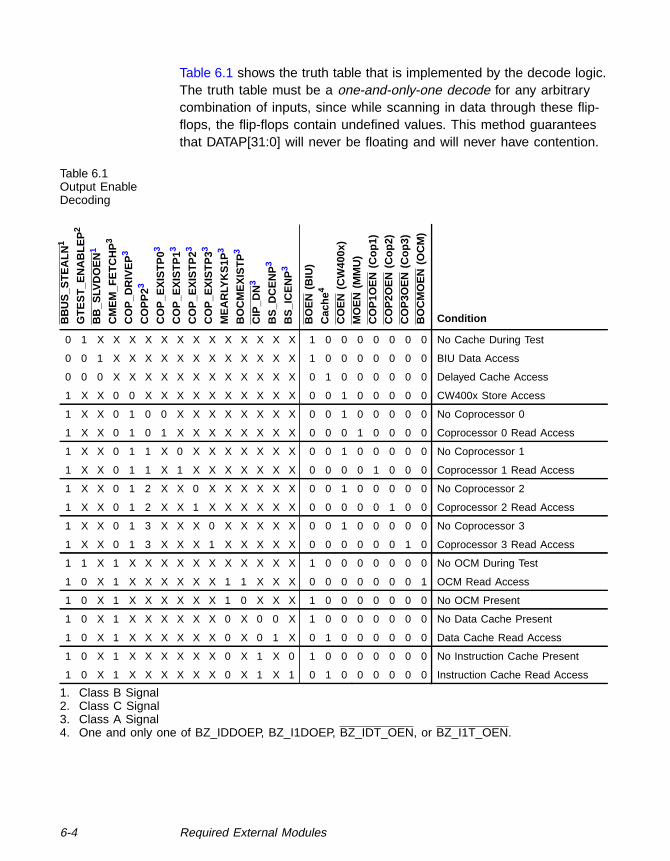
6-4 Required External Modules
Table 6.1 shows the truth table that is implemented by the decode logic.The truth table must be a one-and-only-one decode for any arbitrarycombination of inputs, since while scanning in data through these flip-flops, the flip-flops contain undefined values. This method guaranteesthat DATAP[31:0] will never be floating and will never have contention.
Table 6.1Output EnableDecoding
BB
US
_ST
EA
LN1
1. Class B Signal
GT
ES
T_E
NA
BLE
P2
2. Class C Signal
BB
_SL
VD
OE
N1
CM
EM
_FE
TC
HP
3
3. Class A Signal
CO
P_D
RIV
EP
3
CO
PP
23
CO
P_E
XIS
TP
03
CO
P_E
XIS
TP
13
CO
P_E
XIS
TP
23
CO
P_E
XIS
TP
33
ME
AR
LYK
S1P
3
BO
CM
EX
IST
P3
CIP
_DN
3
BS
_DC
EN
P3
BS
_IC
EN
P3
BO
EN
(BIU
)
Cac
he4
4. One and only one of BZ_IDDOEP, BZ_I1DOEP, BZ_IDT_OEN, or BZ_I1T_OEN.
CO
EN
(CW
400x
)
MO
EN
(MM
U)
CO
P1O
EN
(Cop
1)
CO
P2O
EN
(Cop
2)
CO
P3O
EN
(Cop
3)
BO
CM
OE
N(O
CM
)
Condition
0 1 X X X X X X X X X X X X X 1 0 0 0 0 0 0 0 No Cache During Test
0 0 1 X X X X X X X X X X X X 1 0 0 0 0 0 0 0 BIU Data Access
0 0 0 X X X X X X X X X X X X 0 1 0 0 0 0 0 0 Delayed Cache Access
1 X X 0 0 X X X X X X X X X X 0 0 1 0 0 0 0 0 CW400x Store Access
1 X X 0 1 0 0 X X X X X X X X 0 0 1 0 0 0 0 0 No Coprocessor 0
1 X X 0 1 0 1 X X X X X X X X 0 0 0 1 0 0 0 0 Coprocessor 0 Read Access
1 X X 0 1 1 X 0 X X X X X X X 0 0 1 0 0 0 0 0 No Coprocessor 1
1 X X 0 1 1 X 1 X X X X X X X 0 0 0 0 1 0 0 0 Coprocessor 1 Read Access
1 X X 0 1 2 X X 0 X X X X X X 0 0 1 0 0 0 0 0 No Coprocessor 2
1 X X 0 1 2 X X 1 X X X X X X 0 0 0 0 0 1 0 0 Coprocessor 2 Read Access
1 X X 0 1 3 X X X 0 X X X X X 0 0 1 0 0 0 0 0 No Coprocessor 3
1 X X 0 1 3 X X X 1 X X X X X 0 0 0 0 0 0 1 0 Coprocessor 3 Read Access
1 1 X 1 X X X X X X X X X X X 1 0 0 0 0 0 0 0 No OCM During Test
1 0 X 1 X X X X X X 1 1 X X X 0 0 0 0 0 0 0 1 OCM Read Access
1 0 X 1 X X X X X X 1 0 X X X 1 0 0 0 0 0 0 0 No OCM Present
1 0 X 1 X X X X X X 0 X 0 0 X 1 0 0 0 0 0 0 0 No Data Cache Present
1 0 X 1 X X X X X X 0 X 0 1 X 0 1 0 0 0 0 0 0 Data Cache Read Access
1 0 X 1 X X X X X X 0 X 1 X 0 1 0 0 0 0 0 0 0 No Instruction Cache Present
1 0 X 1 X X X X X X 0 X 1 X 1 0 1 0 0 0 0 0 0 Instruction Cache Read Access

Global Output Enable Module (GOE) 6-5
The only problem with the design in Figure 6.1 is that the output enablesmust have a very fast delay from the clock signals. Therefore, the logicalthing to do is to move the decode logic in front of the flip-flops. Thisdesign latches all of the output enables, but presents a problem. If wemove the logic in front of the scan chain muxes, the flip-flops will containrandom values and so one-and-only-one decode cannot be guaranteedduring scan.
To solve this problem, LSI Logic implemented the scheme in Figure 6.2.This design is functionally equivalent to Figure 6.1, but with improved tim-ing.
Figure 6.2Improved TimingGOE Design Logic
This design would solve all of these problems if not for RUN_INN.RUN_INN is a very late signal, so the design must be optimized to allowRUN_INN to be as late as possible. Therefore, Figure 6.3 shows the finaldesign solution.
FD1
Class A Signal
Class B Signal
Decode OutputEnables
0
1
RUN_INN
Scan In
GSCAN_ENABLEP
Scan Out
Class C Signal
0
1
Scan In
Scan Out0
1
GSCAN_ENABLEP
FD1
FD1

6-6 Required External Modules
Figure 6.3Final GOE DesignLogic
This final version of the GOE has duplicated the decode logic as well asthe scan mux. This allows us to pre-compute the output enables for bothcases of RUN_INN LOW (0) and RUN_INN HIGH (1). Then we selectthe correct output enable, using a mux, when RUN_INN becomes valid.This circuit is functionally equivalent in every way to the originalfunctional circuit (Figure 6.1).
To use ATPG software, the logic should be replaced with the originalcircuit (Figure 6.1), since the flip-flops are not strictly scannable (soATPG would treat them as non-scanned flip-flops and lower thecoverage).
Decode
Class A Signal
Class B Signal
Decode
OutputEnables
0
1
RUN_INN
FD1 Scan Out
Class C Signal
0
1
Scan In
Scan Out0
1
GSCAN_ENABLEP
0
1
0
1 0
1
RUN_INN
FD1
FD1
Scan In

Global Output Enable Module (GOE) 6-7
6.1.1.2 Run Enables
All of the module Run Request Signals (BRUN_OUTP, CRUN_OUTP,MRUN_OUTP, GRUN_OUT1P, and GRUN_OUT2P) must be combinedto form a Global Run Enable Signal (RUN_INN). The GOE generatesthree copies of this signal (BRUN_INN, CRUN_INN, and MRUN_INN) forthe CW400x and all other peripherals (see Figure 6.4).
Figure 6.4Creation ofRUN_INN
6.1.1.3 Pipeline Run Indicator
All of the module run request signals (BRUN_OUTP, CRUN_OUTP,MRUN_OUTP, GRUN_OUT1P, GRUN_OUT2P) and CIP_DN must becombined to form the Pipeline Run Indicator Signal, CPIPE_RUNN (seeFigure 6.5).
Figure 6.5Creation ofCPIPE_RUNN
6.1.2Signals
This section describes the signals that comprise the bit-level interface ofthe GOE.
The signals are described in alphabetical order by mnemonic. Eachsignal definition contains the mnemonic and the full signal name. Themnemonics for signals that are active LOW end in an “N” and have anoverbar, and the mnemonics for signals that are active HIGH end in a “P.”
In the descriptions that follow, the verb assert means to drive TRUE oractive. The verb deassert means to drive FALSE or inactive.
BRUN_OUTP
BRUN_INN
CRUN_INN
MRUN_INN
CRUN_OUTPMRUN_OUTP
RUN_INN
GRUN_OUT1PGRUN_OUT2P
CIP_DNBRUN_OUTPCRUN_OUTPMRUN_OUTP
GRUN_OUT1PGRUN_OUT2P
CPIPE_RUNN

6-8 Required External Modules
6.1.2.1 Class A Signals
These signals are valid only on Bus Run Cycles (for a definition of BusRun Cycles see Section 7.1.3, “Operation and Functional Waveforms”).
BOCMEXISTP On-Chip Memory (OCM) Memory Present InputAsserting this signal indicates that the OCM is present.This signal is also an input to the OCM. The systemdesigner ties this to power (HIGH) to indicate OCMpresent, and to ground (LOW) to indicate OCM notpresent.
BS_DCENP Data Cache Enabled InputThis signal is accessed through a bit in the BBCC Con-figuration Register, BS_CONFIGP0. Asserting this signalinforms the GOE that the data cache is enabled.
BS_ICENP Instruction Cache Enabled InputThis signal is accessed through a bit in the BBCC Con-figuration Register, BS_CONFIGP4. Asserting this signalinforms the GOE that the instruction cache is enabled.
CIP_DN CW400x Instruction/Data Indication InputThis signal qualifies the type of memory fetch when amemory fetch is indicated by CMEM_FETCHP. TheCW400x drives this signal HIGH to indicate that it is per-forming an instruction fetch. The CW400x drives this sig-nal LOW to indicate that it is performing a data fetch.
CMEM_FETCHPCW400x Memory Fetch Request InputThe CW400x asserts this signal HIGH to indicate that itis performing a memory fetch.
COP_DRIVEP Coprocessor Drives Data Bus Indicator InputThe CW400x asserts this signal HIGH to inform the GOEthat a coprocessor should drive DATAP[31:0].
COPEXISTP[3:0] Coprocessors exist InputThe coprocessors assert these signals to indicate to theGOE which coprocessors are present.
COPP[1:0] Coprocessor Number InputOutput from the CW400x. These signals from the coreindicate to the GOE which coprocessor should driveDATAP[31:0].

Global Output Enable Module (GOE) 6-9
MEARLYKS1P Stub Early kseg1 Signal InputThe MMU Stub asserts this signal HIGH to indicate thatthe virtual address is in kseg1. MEARLYKS1P is a com-binational feed-through path based on the ADDRP[31:0]inputs. This signal is for devices that may require an earlyindication of the virtual memory area for a pending mem-ory cycle. It provides access information before the risingedge of the clock beginning the bus cycle. This signal isan input to the Bus Interface Unit. (BIU)
6.1.2.2 Class B Signals
These signals are valid at every clock cycle. Note that LSI Logic’s BBCCcontains a BIU.
BB_SLVDOEN BIU Bus Slave Drive Request InputThe BIU asserts this signal LOW to inform the GOE thatthe BIU is a bus slave and that the external device isrequesting a read access to the caches. This signal indi-cates that one of the cache RAMs will drive the bus start-ing at the rising edge of the next clock cycle.
BBUS_STEALNBIU Bus Steal InputThe BIU asserts this signal LOW to inform the GOE thatthe BIU will become the Data Bus Master starting at therising edge of the next clock cycle.
6.1.2.3 Class C Signals
These signals do not need to be latched. They are static for the purposesof decode.
GTEST_ENABLEPTest Enable InputAsserting this signal HIGH enables scan testing of thechip’s system logic. Note that this signal must always beasserted during a scan test. Note also that this signal isused raw (not latched at all). (For more information onscan testing see Section 8.2, “Scan Methodology”.)
GSCAN_ENABLEPScan Test Mode Enable InputAsserting this signal enables loading of the scan chain.

6-10 Required External Modules
6.1.2.4 Run/Stall Signals
These signals control and indicate the run/stall state of the system.
CPIPE_RUNN CW400x Pipeline Run Indicator OutputThe GOE asserts this signal LOW to inform the FlexLinkComputational Unit that the core is in a pipeline runcycle. The GOE deasserts this signal HIGH to inform theComputational Unit that the core is in a pipeline stallcycle.
CRUN_INN CW400x Run Enable OutputThe GOE asserts this signal LOW to enable the core togo on to the next run cycle. The GOE deasserts this sig-nal HIGH to stall the core.
CRUN_OUTP CW400x Run Request InputThe core asserts this signal HIGH to request to the GOEthat it go on to the next run cycle. The core deasserts thissignal LOW to request stalling the pipeline.
BRUN_INN BIU Run Enable OutputThe GOE asserts this signal LOW to enable the BIU togo on to the next run cycle. The GOE deasserts this sig-nal HIGH to stall the BIU.
BRUN_OUTP BIU Run Request InputThe BIU asserts this signal HIGH to request to the GOEthat it go on to the next run cycle. The BIU deasserts thissignal LOW to request stalling the pipeline.
GRUN_OUT1P General Device Run Request 1 InputGeneral Device 1 asserts this signal HIGH to request tothe GOE that it go on to the next run cycle. GeneralDevice 1 deasserts this signal LOW to request stallingthe pipeline.
GRUN_OUT2P General Device Run Request 2 InputGeneral Device 2 asserts this signal HIGH to request tothe GOE that it go on to the next run cycle. GeneralDevice 2 deasserts this signal LOW to request stallingthe pipeline.

Global Output Enable Module (GOE) 6-11
MRUN_INN External Device Run Enable OutputThe GOE asserts this signal LOW to enable the MMU togo on to the next run cycle. The GOE deasserts this sig-nal HIGH to stall the MMU.
MRUN_OUTP MMU Run Request InputThe MMU asserts this signal HIGH to request to the GOEthat it go on to the next run cycle. The MMU deassertsthis signal LOW to request stalling the pipeline.
6.1.2.5 GOE Output Enables
These signals are all valid every cycle and are designed to be hookedstraight into the output enables (after a buffer) for various modules. Onlyone of these signals (including also the BBCC Output Enables) can beasserted (enabling the device) at a time.
COEN CW400x Output Enable OutputInput to the CW400x. The GOE asserts this signal toenable the core to drive data onto DATAP[31:0].
BIUOEN BIU Output Enable OutputInput to the BIU. The GOE asserts this signal to enablethe BIU to drive data onto DATAP[31:0].
MOEN MMU (COP0) Output Enable OutputInput to the MMU. The GOE asserts this signal to enablethe MMU to drive data onto DATAP[31:0].
COP1OEN Coprocessor 1 Output Enable OutputInput to Coprocessor 1 (FPU). The GOE asserts this sig-nal to enable Coprocessor 1 (FPU) to drive data ontoDATAP[31:0].
COP2OEN Coprocessor 2 Output Enable OutputInput to Coprocessor 2. The GOE asserts this signal toenable Coprocessor 2 to drive data onto DATAP[31:0].
COP3OEN Coprocessor 3 Output Enable OutputInput to Coprocessor 3. The GOE asserts this signal toenable Coprocessor 3 to drive data onto DATAP[31:0].

6-12 Required External Modules
6.1.2.6 BBCC Output Enables
These signals are outputs from the BBCC, not the GOE (see Figure 6.6).Their operation is described here anyway, since they are part of the GOEfunction. The user must remember that the decodes for these signals arefixed and cannot be altered. These signals are all valid every cycle andare designed to be hooked straight into the input enables (after a buffer)for various modules. Only one of these signals (including also the GOEOutput Enables) can be asserted (enabling the device) at a time. (Seethe MiniRISC Building Blocks Technical Manual for more informationabout the BBCC, the 3-state gates, and the Cache System.)
BZ_IDDOEP I-Cache Set 0/D-Cache Data RAM Output Enable Out-putInput to the I-Cache Set 0/D-Cache Data RAM from theBBCC. The BBCC asserts this signal to enable the datafrom the I-Cache Set 0/D-Cache Data RAM to drive dataonto DATAP[31:0].
BZ_I1DOEP I-Cache Set 1 Data RAM Output Enable OutputInput to the I-Cache Set 1 Data RAM from the BBCC.The BBCC asserts this signal to enable the I-Cache Set1 Data RAM to drive data onto DATAP[31:0].
BZ_IDT_OEN I-Cache Set 0/D-Cache Tag RAM Output Enable Out-putInput to a set of 3-state gates from the BBCC. The BBCCasserts this signal to enable a set of 3-state gates todrive data from the I-Cache Set 0/D-Cache Tag RAMonto DATAP[31:0].
BZ_I1T_OEN I-Cache Set 1 Tag RAM Output Enable OutputInput to a set of 3-state gates from the BBCC. The BBCCasserts this signal to enable a set of 3-state gates todrive data from the I-Cache Set 1 Tag RAM ontoDATAP[31:0].
BOCMOEN On-Chip Memory (OCM) Output Enable OutputInput to the OCM from the BBCC. The BBCC asserts thissignal to enable the OCM to drive data onto DATAP[31:0].

Global Output Enable Module (GOE) 6-13
6.1.3Connecting tothe CW400x andBuilding Blocks
Figure 6.6 shows how to attach the GOE to the CW400x and buildingblocks.
Figure 6.6GOE ModuleAttachments
BRUN_INN
BRUN_OUTP
COP2OEN
MRUN_INN
MOEN
MRUN_OUTP
MEARLYKS1P
GSCAN_ENABLEP
GTEST_ENABLEP
COEN
COP_DRIVEP
COPP[1:0]
CRUN_OUTP
CRUN_INN
CMEM_FETCHP
CIP_DN
CW400xGOE
Coprocessor 1
CPIPE_RUNN
COPEXISTP2
COPEXISTP3
COP3OEN
COP1OEN
COPEXISTP1
Coprocessor 2
Coprocessor 3
BIU
BIUOEN
BB_SLVDOEN
BBUS_STEALN
MMU
COPEXISTP0
BS_CONFIGP0
BOCMOENBOCMEXISTP OCM
GRUN_OUT1P
GRUN_OUT2P
(BBCC)
CacheSystem
BS_CONFIGP4
BZ_IDDOEP
BZ_I1DOEP
BZ_IDT_OEN
BZ_I1T_OEP
(BS_DCENP)
(BS_ICENP)
Tied to Ground or Power

6-14 Required External Modules
6.2MMU Stub
The MMU Stub is required as an external module if there is no MMUattached to the CW400x. Both the MMU and MMU Stub latch and holdthe address bus through stalls and also direct-map the kseg0 and kseg1(kernel segments 0 and 1) virtual address space onto the first 512Mbytes of physical address space.
The MiniRISC CW400x drives addresses onto the Address Bus,ADDRP[31:0]. Although CW400x-based systems do not require a fullMMU, in most cases, some of the functions of the MMU are required forthe system to maintain both MIPS compatibility and ease of design. LSILogic provides the MMU Stub to perform these tasks.
6.2.1Function
The MMU Stub takes addresses from the MiniRISC CW400x Core andregisters them. This address registration is useful because the CW400xdoes not hold the address valid for an entire bus cycle, but rather, holdsit only around the rising clock edge beginning the bus cycle. The MMUStub registers the address for the entire bus cycle. In addition, it trans-lates the addresses in kseg0 or kseg1 to the lower 512 MBytes of Phys-ical Memory, as in the MIPS standard memory map. This translation isthe only address translation performed by the MMU Stub, and as such,is referred to as a hard map. Figure 6.7 shows the MMU Stub hard map.

MMU Stub 6-15
Figure 6.7MMU Stub HardAddress Mapping (HardMap)
Since the output address is transformed when in kseg0 and kseg1, theMMU Stub generates signals indicating that the address from theCW400x was in kseg0/1/2 (KSEGCHECKP), and more precisely, if it wasin kseg1 (KSEG1_NOCACHEP).
6.2.2Signals
This section describes the signals that comprise the bit-level interface ofthe MMU Stub.
The signals are described in alphabetical order by mnemonic. Eachsignal definition contains the mnemonic and the full signal name. The
0xFFFF FFFFkseg2
kseg1
kseg0
kuseg
0x8000 0000
0xA000 0000
0xC000 0000
0xFFFF FFFF
0x0000 0000
Microprocessor Address Real Memory
UserCached
KernelCached
KernelUncached
KernelCached
32-Bit Address4 GB Memory
512 MBytes
0x2000 0000
0x0000 0000

6-16 Required External Modules
mnemonics for signals that are active LOW end in an “N” and have anoverbar, and the mnemonics for signals that are active HIGH end in a “P”(except LVIRADDR_31, LVIRADDR_30, and LVIRADDR_29).
In the descriptions that follow, the verb assert means to drive TRUE oractive. The verb deassert means to drive FALSE or inactive.
ADDRP[31:0] CW400x Address Bus InputThe core drives these signals with the memory address.
GSCAN_ENABLEPScan Test Mode Enable InputSystem logic asserts this signal HIGH to enable scantesting.
GSCAN_INP Scan Test Input InputThis signal is the input to the internal scan chain.
GSCAN_OUTP Scan Test Output OutputThis signal is the output from the internal scan chain.
KSEG1_NOCACHEPkseg1 Indicator OutputThe MMU Stub asserts this signal HIGH to indicate thatthe Stub has detected an address from the CW400x inkseg1 space, indicating that this data transaction shouldnot be cached.
KSEGCHECKP kseg0/1/2 Indicator OutputThe MMU Stub asserts this signal HIGH to indicate thatthe MMU Stub has detected an address from theCW400x in kernel space. This signal is an input to theBus Interface Unit.
LVIRADDR_29 CW400x Address Bit 29 OutputThis signal is the registered version of the CW400xAddress Bit 29, unmapped. This signal is an input to theBus Interface Unit.
LVIRADDR_30 CW400x Address Bit 30 OutputThis signal is the registered version of the CW400xAddress Bit 30, unmapped. This signal is an input to theBus Interface Unit.

MMU Stub 6-17
LVIRADDR_31 CW400x Address Bit 31 OutputThis signal is the registered version of the CW400xAddress Bit 31, unmapped. This signal is an input to theBus Interface Unit.
MEARLYKS1P Stub Early kseg1 Signal OutputThe MMU Stub asserts this signal HIGH to indicate thatthe virtual address is in kseg1. MEARLYKS1P is a com-binational feed-through path based on the ADDRP[31:0]inputs. This signal is for devices that may require an earlyindication of the virtual memory area for a pending mem-ory cycle. It provides access information before the risingedge of the clock beginning the bus cycle. This signal isan input to the Bus Interface Unit.
MRUN_INN External Device Run Signal InputDeasserting this signal HIGH indicates that some othermodule is stalling the CBus. The MMU Stub only clocksin new addresses during Bus Run Cycles.
PCLKP System Clock InputThis signal is the global clock input. It is used to clockelements in the MMU Stub.
REG_ADDRP[31:0]CW400x Address Bus OutputThese signals are the registered, translated CW400xAddress Bus. These signals are inputs to the Bus Inter-face Unit.
6.2.3Connecting tothe CW400x
In order to connect the MMU Stub to the CW400x correctly, simply con-nect the ADDRP[31:0] Inputs to the ADDRP[31:0] Outputs of theCW400x. Connect the MRUN_INN input to a gate that logically NANDsall Run Indication Signals in the system, so that the MRUN_INN signalis active only if all the Run Indication Signals are indicating run (this logicis found in the GOE Module). The MMU Scan Inputs(GSCAN_ENABLEP and GSCAN_INP) should be connected to the Glo-bal Scan Enable and the Scan Out of another module’s scan chain. Theother signals connect to a BIU.

6-18 Required External Modules
Figure 6.8 shows a block diagram of the logical I/O connections for theMMU Stub.
Figure 6.8MMU StubAttachments
CW400x
ADDRP[31:0]
KSEG1_NOCACHEP
KSEGCHECKP
MEARLYKS1P
LVIRADDR_29
LVIRADDR_30
LVIRADDR_31
REG_ADDRP[31:0]
MMU Stub
System MRUN_INN
BIU
PCLKP
ADDRP[31:0]
PCLKP
GSCAN_ENABLEP
GSCAN_INP
GSCAN_OUTP
Scan Chain Test Output
Global Scan Enable
NAND of allRun IndicationSignals From
from Another Module
GOE
Clock
Scan Chain TestInput to AnotherModule

7-1
Chapter 7Interfaces
This chapter describes the interfaces for the CW400x Microprocessor. Itcontains the following sections:
♦ Section 7.1, “CBus Interface”
♦ Section 7.2, “FlexLink Interface”
7.1CBus Interface
The CBus Interface is the main link between the CW400x Microproces-sor and logic, such as an MMU, BIU (Bus Interface Unit), Cache, andCoprocessors. The BIU is external to the core (see Figure 1.1). The usermust either create a BIU according to the information in this section, oruse LSI Logic’s BBCC.
7.1.1Bus Stealing
To allow the BIU to implement instruction streaming and load schedulingefficiently, the BIU can assert BBUS_STEALN to steal Data Bus(DATAP[31:0]) cycles away from the CW400x. When BBUS_STEALN isasserted, any module which is driving DATAP[31:0] must release it. TheBIU will then be guaranteed that it can drive DATAP[31:0] without con-tention. The BIU can then do an operation such as block refill, insert datafor a load, DMA transfers, or cache snooping.
If a cycle is stolen in a X2 Stage, the CW400x stalls to guarantee thatthe last X2 Cycle will not be stolen for Stores, MTCz, MFCz, CTCz, andCFCz Instructions. This simplifies the coprocessor’s interface design.
7.1.2InterfaceSignals
The CW400x CBus Interface consists of the signals shown in Table 7.1.Signal direction is relative to the CW400x. For more detail on thesesignals see Chapter 3.

7-2 Interfaces
Table 7.1CW400x CBusInterface Signals
7.1.3Operation andFunctionalWaveforms
CW400x Microprocessor transactions occur during Bus Run Cycles.Asserting CRUN_INN causes the following clock cycle to be a Bus RunCycle. The states of CIP_DN, CMEM_FETCHP, and CSTOREP in thecycle before the Bus Run Cycle specify what type of transaction willoccur during the Bus Run Cycle.
7.1.3.1 Instruction Fetches
Instruction Fetch Protocol Rules:
1. The CW400x asserts CMEM_FETCHP before the rising edge of theBus Run Cycle to initiate a fetch request from memory.CMEM_FETCHP is only valid during Bus Run Cycles.
2. The CW400x drives CIP_DN HIGH before the rising edge of the BusRun Cycle to initiate an instruction transfer. CIP_DN is only valid dur-ing Bus Run Cycles.
3. The CW400x drives the address of the instruction to be fetched onADDRP[31:0] before the rising edge of the Bus Run Cycle.ADDRP[31:0] is only valid during the Bus Run Cycle. It is not heldduring stall cycles. If the system designer needs to store the address
Signal Definition I/O
ADDRP[31:0] Address Bus Output
BBEP BIU Bus Error Input
BBIG_ENDIANP Big Endian Select Input
BDRDYP BIU Load Data Ready Input
BIRDYP BIU Instruction Data Ready Input
CADDR_ERRORP Memory Address Error Output
CBYTEP[3:0] Byte Enables Output
CIP_DN CW400x Instruction/Data Indication Output
CKILLMEMP Kill Memory Transaction Output
CMEM_FETCHP CW400x Memory Fetch Request Output
COEN CW400x Output Enable Input
CRUN_INN CW400x Run Enable Input
CRUN_OUTP CW400x Run Request Output
CSTOREP CW400x Store to Memory Request Output
DATAP[31:0] CW400x Data Bus Bidirectional

CBus Interface 7-3
externally during stalls, he/she must either use the MMU Stub, orattatch external flip-flops that are clocked during the beginning of theBus Run Cycle.
4. The BIU must drive DATAP[31:0] with the requested instruction andassert BIRDYP to tell the CW400x that valid data is on the data bus.If the instruction cannot be provided by the end of the Bus RunCycle, the CW400x deasserts CRUN_OUTP to stall the pipe. Oncethe data is valid on the bus, the BIU must assert BIRDYP.
5. The CW400x asserts CKILLMEMP if the outstanding instructionrequest must be killed (a TLB miss or an address error for example).The BIU may assert BIRDYP in the same cycle as CKILLMEMP butmust not assert BIRDYP in the following cycles of the instructionrequest. CKILLMEMP will only be asserted during the Bus RunCycles.
6. Upon a bus error, the BIU must assert BBEP and BIRDYP.

7-4 Interfaces
Figure 7.1 shows four instruction fetches.
Figure 7.1Instruction FetchExamples 1
1. Instruction fetch with an instruction cache hit.2. Instruction fetch with an instruction cache miss.3. Instruction fetch with an instruction cache miss and some other external stall.4. Instruction fetch with an instruction bus error.
2-IF 3-IF1-IF 4-IF
Bus Run Bus Stall Bus Run Bus Stall Bus Stall Bus Run Bus StallBus Run
MD95.177
PCLKP
CRUN_INN
CRUN_OUTP
CIP_DN
ADDRP[31:0]
CMEM_FETCHP
CSTOREP
DATAP[31:0]
BIRDYP
BBUS_STEALN
BBEP
1 2 3 4
1 2 3

CBus Interface 7-5
Figure 7.2 shows four more instruction fetches.
Figure 7.2Instruction FetchExample 2
7.1.3.2 Data Loads
Data Load Protocol Rules:
1. The CW400x asserts CMEM_FETCHP before the rising edge of theX2 Stage Bus Run Cycle to initiate a fetch request from memory.CMEM_FETCHP is only valid during Bus Run Cycles.
1. Instruction fetch with an instruction cache hit followed by a bus steal.2. Instruction fetch which is killed (TLB miss or address error).3. Instruction fetch with an instruction cache miss and a bus steal.4. Instruction fetch with an instruction cache miss, instruction on bus during steal cycle and exter-
nal stall. Note that the last cycle of 4-IF is a stall cycle even though CRUN_OUTP is HIGHbecause there is an external stall request present (CRUN_INN HIGH).
2-IF 3-IF1-IF 4-IF
Bus Run Bus Run Bus Stall Bus Stall Bus Run Bus Stall Bus StallBus Run
MD95.178
PCLKP
CRUN_INN
CRUN_OUTP
CIP_DN
ADDRP[31:0]
CMEM_FETCHP
CSTOREP
DATAP[31:0]
BIRDYP
BBUS_STEALN
CKILL_MEMP
21 3 4
1 BIU BIU 3 BIU-4

7-6 Interfaces
2. The CW400x drives CIP_DN LOW before the rising edge of the X2Stage Bus Run Cycle to indicate a data transfer. CIP_DN is onlyvalid during Bus Run Cycles.
3. During the first cycle of the X2 Stage, there is a Bus Run Cycle, butinternally, the CW400x stalls the pipe.
4. The CW400x drives the address of the data to be fetched onADDRP[31:0] before the rising edge of the Bus Run Cycle.ADDRP[31:0] is only valid during the Bus Run Cycle. It is not heldduring stall cycles.
5. The CW400x asserts CBYTEP[3:0] before the rising edge of the X2Stage Bus Run Cycle to distinguish which bytes are to be fetched.CBYTEP[3:0] remains asserted until the end of the X2 Stage. Notethat CBYTEP[3:0] is an X Stage signal, so it must not be used in theBIU instruction fetch logic.
6. The BIU drives DATAP[31:0] with the requested data and assertsBDRDYP.
Non-scheduleable Loads. If the BIU cannot provide the requesteddata by the end of the Bus Run Cycle and the load is not sched-uleable (LWL and LWR Instructions), the CW400x continues to stallthe pipe until BDRDYP is asserted. Note that the BIU is not requiredto use the BBUS_STEALN to provide the requested data.
Scheduleable Loads. If the BIU cannot provide the requested databy the end of the Bus Run Cycle and the load is scheduleable, theCW400x releases the stall and continues the pipe. Once the data isready, the BIU must assert BBUS_STEALN, drive the requested dataonto the DATAP[31:0], and assert BDRDYP. If the scheduled load hasa data dependency or another load enters the X1 Stage, theCW400x stalls the pipe in the X1 Stage and waits for the BIU to pro-vide the scheduled load data.
No Scheduling for Scheduleable Loads. If the BIU cannot providethe requested data by the end of the Bus Run Cycle and the load isscheduleable, the user may choose to not implement load schedulingby deasserting CRUN_INN (stalling the core) until BDRDYP isasserted. Not implementing load scheduling simplifies the BIUdesign.
7. The CW400x asserts CKILLMEMP if the outstanding data requestmust be killed (such as when a TLB miss or address error occurs).The BIU may assert BDRDYP in the same cycle as CKILLMEMP but
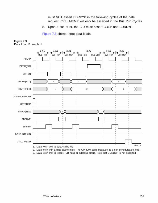
CBus Interface 7-7
must NOT assert BDRDYP in the following cycles of the datarequest. CKILLMEMP will only be asserted in the Bus Run Cycles.
8. Upon a bus error, the BIU must assert BBEP and BDRDYP.
Figure 7.3 shows three data loads.
Figure 7.3Data Load Example 1
1. Data fetch with a data cache hit.2. Data fetch with a data cache miss. The CW400x stalls because its a non-scheduleable load.3. Data fetch that is killed (TLB miss or address error). Note that BDRDYP is not asserted.
1-X2 2-X1 2-X2 3-X11-X1 3-X2
Bus Run Bus Run Bus Run Bus Stall Bus Run Bus RunBus Run
MD95.179
PCLKP
CRUN_INN
CIP_DN
ADDRP[31:0]
CBYTEP[3:0]
CMEM_FETCHP
CSTOREP
DATAP[31:0]
BDRDYP
BIRDYP
BBUS_STEALN
CKILL_MEMP
1 2 3
1 2 3
1 2

7-8 Interfaces
Figure 7.4 shows two more data loads.
Figure 7.4Data Load Example 2
1a.Data fetch with a data cache miss and scheduled load.1b. Scheduled load data fetched.2. Data fetch (non-scheduleable) with a bus error. Note that BDRDYP is asserted for bus error.
1-X2 2-X11-X1 2-X2
Bus Run Bus Run Bus Stall Bus Run Bus Run Bus StallBus Run
MD95.180
PCLKP
CRUN_INN
CIP_DN
ADDRP[31:0]
CBYTEP[3:0]
CMEM_FETCHP
CSTOREP
DATAP[31:0]
BDRDYP
BIRDYP
BBUS_STEALN
CKILL_MEMP
1a 2
1a 2
BIU-1b

CBus Interface 7-9
Figure 7.5 shows a non-scheduleable data load with a data cache missinterrupted by a bus steal. Note that BBUS_STEALN was not assertedfor a scheduled load or instruction refill.
Figure 7.5Data LoadExample 3
1-X21-X1
Bus Run Bus Stall Bus StallBus Run
MD95.181-1
PCLKP
CRUN_INN
CIP_DN
ADDRP[31:0]
CMEM_FETCHP
CSTOREP
DATAP[31:0]
BDRDYP
BIRDYP
BBUS_STEALN
CBYTEP[3:0]
1
1
BIU 1

7-10 Interfaces
Figure 7.6 shows a previously scheduled data load forcing a stall in theX1 Stage of another load that has a data cache hit.
Figure 7.6Data LoadExample 4
7.1.3.3 Data Stores
Data Store Protocol Rules:
1. The CW400x asserts CSTOREP before the rising edge of the X2Stage Bus Run Cycle to indicate a store request. CSTOREP is onlyvalid during Bus Run Cycles. The CW400x will never assertCMEM_FETCHP and CSTOREP in the same Bus Run Cycle.
2. The CW400x drives CIP_DN LOW before the rising edge of the X2Stage Bus Run Cycle to indicate a data transfer. CIP_DN is onlyvalid during Bus Run Cycles.
3. The CW400x asserts the address of the data to be stored onADDRP[31:0] before the rising edge of the X2 Stage Bus Run Cycle.The address is only valid during the Bus Run X2 Cycle. It is not heldduring stalls.
2-X1 2-X2
Bus Run Bus Stall Bus Stall Bus Run
MD95.181-2
PCLKP
CRUN_INN
CIP_DN
ADDRP[31:0]
CMEM_FETCHP
CSTOREP
DATAP[31:0]
BDRDYP
BIRDYP
BBUS_STEALN
CBYTEP[3:0]
2
2
BIU 2

CBus Interface 7-11
4. The CW400x asserts CBYTEP[3:0] before the rising edge of the X2Stage Bus Run Cycle to indicate which bytes are to be stored.CBYTEP[3:0] continues to be asserted until the end of the X2 Stage.
5. During the first cycle of the X2 Stage, there is a Bus Run Cycle, butinternally, the CW400x stalls the pipe.
6. The BIU must assert COEN during the X2 Stage. The CW400xdrives the requested data onto DATAP[31:0] in the X2 Stage Bus RunCycle and following stall cycles.
7. When the BIU asserts BBUS_STEALN, it must also deassert COENduring the following cycle to 3-state DATAP[31:0]. AfterBBUS_STEALN is deasserted, the CW400x stalls the pipe for onemore cycle to guarantee that the CW400x will drive the DATAP[31:0]with the store data in the last X2 Cycle. If BBUS_STEALN isasserted during the X1 Stage, the CW400x continues into the X2Stage but does not drive DATAP[31:0]. To help make the design pro-cess easier, designers may choose to use the existing external mod-ule, the GOE, which contains the logic for controlling COEN asdescribed above.
8. The BIU must deassert CRUN_INN to stall the pipe if one non-stolenX2 Cycle is not sufficient (such as a store miss) and register theaddress if needed (the MMU or MMU Stub may already do this).
9. The CW400x asserts CKILLMEMP if the outstanding data store mustbe killed (due to a TLB miss or address error for example). CKILL-MEMP will only be asserted in the Bus Run Cycles.
10. During stalls, the CW400x continues to drive DATAP[31:0] until theend of the X2 Stage.
11. An external stall in the X1 Stage prevents the CW400x from enteringthe X2 Stage.
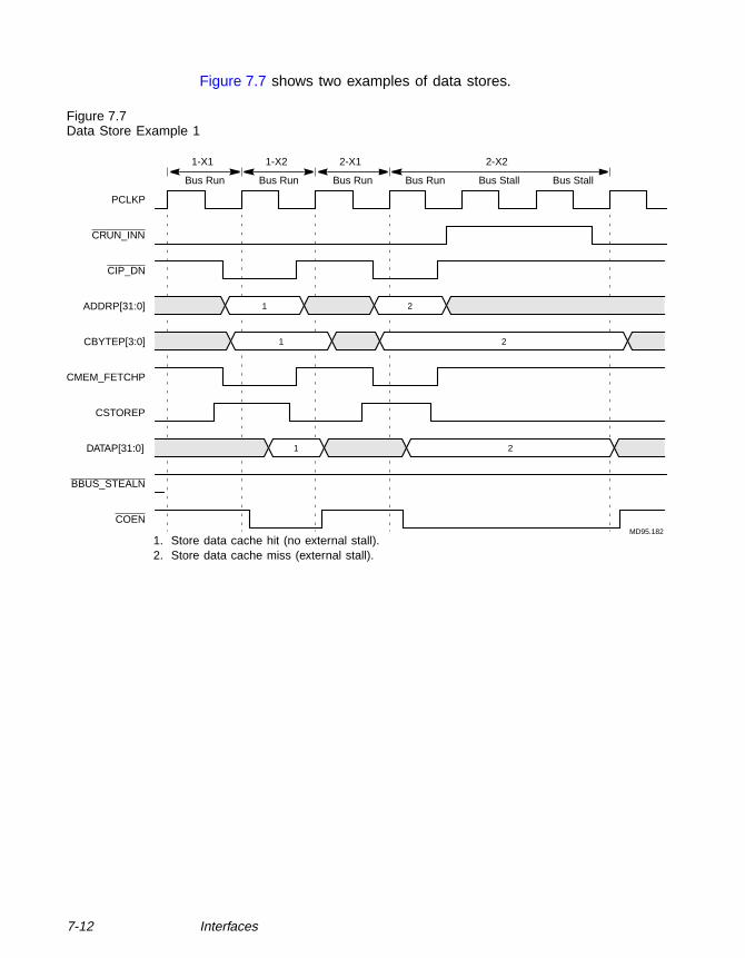
7-12 Interfaces
Figure 7.7 shows two examples of data stores.
Figure 7.7Data Store Example 1
1-X2 2-X11-X1 2-X2
Bus Run Bus Run Bus Run Bus Stall Bus StallBus Run
PCLKP
CRUN_INN
CIP_DN
ADDRP[31:0]
CMEM_FETCHP
CSTOREP
DATAP[31:0]
BBUS_STEALN
COEN
1. Store data cache hit (no external stall).2. Store data cache miss (external stall).
MD95.182
CBYTEP[3:0]
1 2
1 2
1 2

FlexLink Interface 7-13
Figure 7.8 shows two more examples of data stores.
Figure 7.8Data Store Examples 2
7.2FlexLinkInterface
The FlexLink Interface allows users to implement extended instructionsand insert extra hardware to speed up existing arithmetic functions. Thisflexibility enables system designers to optimize system performance andminimize silicon area. The hardware that is attached to the FlexLink Inter-face is referred to as a Computational Unit in the rest of this document.
Example applications: users can use the FlexLink Interface to connect ahigh-performance multiply-accumulate unit, such as LSI Logic’s MDU(see the MiniRISC Building Blocks Technical Manual), a Fast FourierTransform (FFT) engine, or a leading-one detector in order to acceleratecertain computational routines for DSP applications.
1-X2 2-X11-X1 2-X2
Bus Run Bus Stall Bus Run Bus Run Bus StallBus Run
MD95.183
Bus Stall
PCLKP
CRUN_INN
CIP_DN
ADDRP[31:0]
CMEM_FETCHP
CSTOREP
DATAP[31:0]
BBUS_STEALN
COEN
1. Store data cache hit interrupted by BBUS_STEALN (the CW400x stalls the pipe to guaranteelast X2 Cycle).
2. Store data cache miss interrupted by BBUS_STEALN.
CBYTEP[3:0]
1 2
1 2
BIU 1 2 BIU 2

7-14 Interfaces
A Computational Unit (CU) defines and decodes its own instructions. Itmay obtain its source operands from either its own register file, theCW400x Register File, or the instruction’s immediate field. At the end ofthe operation, it writes the result back to the CW400x Register File.Alternatively, it can write the result back to its own register file. This isparticularly useful in multicycle operations since the CW400x does notneed to be stalled to wait for the result.
7.2.1InterfaceSignals
The CW400x FlexLink Interface consists of the signals shown in Tables7.2 and 7.3. Table 7.2 shows the signals that interface with the CW400xCore (I/O direction relative to the CW400x Core). Table 7.3 shows addi-tional signals that interface with the CU (I/O direction relative to thesystem logic). For more detail on these signals see Chapter 3.
Table 7.2CW400x FlexLinkInterface Signals
Signal Definition I/O 1
1. Input to CW400x from CU. Output from CW400x to CU.
ASELP Computational Unit Select Input
ASTALLP Computational Unit Stall Request Input
AXBUSP[31:0] Computational Unit Result Bus Input
CIR_BOTP[5:0] Instruction Register Bottom Six Bits Output
CIR_TOPP[5:0] Instruction Register Top Six Bits Output
CKILLXP Kill Instruction in Execute Stage Output
CRSP[31:0] CW400x Source Register (rs ) Bus Output
CRTP[31:0] CW400x Source Register (rt ) Bus Output
CRX_VALIDN Register Buses Valid Output

FlexLink Interface 7-15
Table 7.3System LogicFlexLink InterfaceSignals
Signal Definition I/O 1
1. Input to system logic from CU. Output from system logic to CU.2. This signal is used by the FlexLink module to determine when the system is
stalling. If, for some reason, the FlexLink module needs to differentiatebetween pipeline stall cycles and bus stall cycles, the CPIPE_RUNN signalmay be substituted for this signal. For most systems these two signals couldbe used interchangeably.
BCPU_RESETN CW400x Reset Output
CRUN_INN2 CW400x Run Enable Output
GSCAN_ENABLEP Scan Test Mode Enable Output
GSCAN_INP Scan Test Input Output
GSCAN_OUTP Scan Test Output Input
PCLKP System Clock Output

7-16 Interfaces
7.2.2ComputationalUnitInstructions
The Computational Unit (CU) Instructions can use any of the availableopcodes shown in Figure 7.9. The CU can support up to a maximum of60 additional instructions: 22 I-type and 38 R-type.
Figure 7.9Opcodes
01234567
0 1 2 3 4 5 6 7CIRP[28:26]
CIRP[31:29]
I-Type
01234567
CIRP[5:3] 0 1 2 3 4 5 6 7
CIRP[2:0]R-Type
Required for R-Type instructionsReserved MIPS-II CW400x InstructionAvailable to be used by the Computational Unit (CU)
KEY
Unimplemented MIPS2 instruction (available to be used by CU; however, ifthe CU uses it to implement a user-defined instruction, users should make sure
MFHI/LO, MTHI/LO Instructions; same reason as above)(available to the CU, but recommended to be used for MULT, DIV,Unimplemented MIPS1 MULT, DIV, MFHI/LO, MTHI/LO Instructions
the CU will mishandle that MIPS2 Instruction as another user-defined instruction.that the unimplemented MIPS2 instruction is not in the instruction stream, otherwise
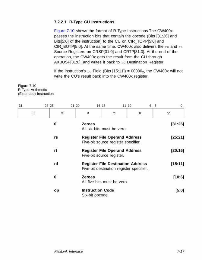
FlexLink Interface 7-17
7.2.2.1 R-Type CU Instructions
Figure 7.10 shows the format of R-Type Instructions.The CW400xpasses the instruction bits that contain the opcode (Bits [31:26] andBits[5:0] of the instruction) to the CU on CIR_TOPP[5:0] andCIR_BOTP[5:0]. At the same time, CW400x also delivers the rs and rt
Source Registers on CRSP[31:0] and CRTP[31:0]. At the end of theoperation, the CW400x gets the result from the CU throughAXBUSP[31:0], and writes it back to rd Destination Register.
If the instruction’s rd Field (Bits [15:11]) = 000002, the CW400x will notwrite the CU’s result back into the CW400x register.
Figure 7.10R-Type Arithmetic(Extended) Instruction
0 Zeroes [31:26]All six bits must be zero.
rs Register File Operand Address [25:21]Five-bit source register specifier.
rt Register File Operand Address [20:16]Five-bit source register.
rd Register File Destination Address [15:11]Five-bit destination register specifier.
0 Zeroes [10:6]All five bits must be zero.
op Instruction Code [5:0]Six-bit opcode.
31 26 25 21 20 16 15 11 10 6 5 0
0 rs rt rd 0 op

7-18 Interfaces
7.2.2.2 I-Type CU Instruction
Figure 7.11 shows the format I-Type Instructions. The CW400x passesthe instruction bits that contain the opcode (Bits [31:26] of the instruction)to the CU on CIR_TOPP[5:0]. At the same time, CW400x also deliversthe rs Source Register and the sign-extended immediate on CRSP[31:0]and CRTP[31:0] respectively. At the end of the operation, the CW400xgets the result from the CU through AXBUSP[31:0], and writes it back tothe rt Destination Register. If the CU wants to have the result writtenback to its own register instead of the CW400x’s, the instruction shouldhave Bits [20:16] = 0.
If the instruction’s rt Field (Bits [20:16]) = 000002, the CW400x will notwrite the CU’s result back into the CW400x Register.
Figure 7.11I-Type Arithmetic(Extended) Instruction
op Instruction Code [31:26]Six-bit opcode.
rs Register File Operand Address [25:21]Five-bit source register specifier.
rt Register File Destination Address [20:16]Five-bit destination register.
immediate 16-bit Immediate [15:0]The sign extends this value to 32 bits and passes it toCRTP[31:0].
7.2.3Operation andFunctionalWaveforms
A CU can implement single or multicycle instructions (instructions whichwrite results back to the CU Registers or the CW400x Registers). Thefollowing text describes a general mechanism for instruction handling.
As soon as the CU decodes a valid instruction, it must assert ASELP toprevent the CW400x from signaling a Reserved Instruction Exception.(The CU must continue to assert ASELP during stalls.) It can then start
31 26 25 21 20 16 15 0
op rs rt immediate

FlexLink Interface 7-19
the operation by using the operands from CRSP[31:0] and CRTP[31:0].The CU has to make sure that CRX_VALIDN is LOW by the end of thatcycle. If CRX_VALIDN is HIGH, it means that the operands it has justobtained are not valid, and it should obtain the operands again in thenext cycle, and restart the operation. The CW400x guarantees at leastone X Cycle where CRX_VALIDN is LOW. If one wants to save power,and performance is less an issue, the CU can check to see ifCRX_VALIDN is LOW before loading the operands off CRSP[31:0] andCRTP[31:0] to start the operation. Depending on where the writeback is,one of the following things will happen:
♦ If the instruction is one which writes the result back to the CW400x’sRegister, the CU has to assert ASTALLP to stall the CW400x untilthe operation is done. The CU deasserts ASTALLP in the same cyclethe CU puts the result onto AXBUSP[31:0]. If, for any reason, theCW400x is still stalling after ASTALLP is deasserted (indicated by aHIGH CRUN_INN), the CU can still keep ASTALLP deasserted, buthas to make sure that a valid result is on AXBUSP[31:0] in the lastcycle before the CW400x goes on to the next run cycle. In order toachieve this, the CU can drive AXBUSP[31:0] the whole time theCW400x is stalling. This whole period when the CU decodes a validinstruction until the CU finishes driving AXBUSP[31:0] is consideredto be an Extended X Stage of the instruction. If CKILLXP is assertedduring this extended X Stage, the CU should kill the instruction, andthe CW400x will make sure that no writeback happens in the end.
♦ For the case where the CU writes the result back to its own registers,the CU does not assert ASTALLP, and the CW400x can continuewith the next instruction. When the operation is finished, the CUwrites the result back to its own registers. Note that in this case,since the CU does not stall the CW400x until the operation is com-plete, the next run cycle after the CU decodes the instruction is nolonger considered to be the X Stage of the instruction. It is the XStage of the next instruction. The CU can ignore any assertion ofCKILLXP or CRUN_INN after it passes the X Stage of an instruction.On the other hand, if the CW400x tries to read the result from theCU Register before it is ready, the CU must stall the Read Instructionby asserting ASTALLP until the result is ready.

7-20 Interfaces
7.2.3.1 Single-cycle Operations
Figure 7.12 shows a typical Computational Unit single-cycle operationthat writes its result into the CW400x CPU Register.
Figure 7.12Computational UnitWrite to CW400x CPURegister
MD95.165
PCLKP
CIR_TOPP[5:0], CIR_BOTP[5:0]
CRSP[31:0], CRTP[31:0]
CRX_VALIDN
ASELP
AXBUSP[31:0]
ASTALLP
CRUN_INN
Instruction
Data
Data

FlexLink Interface 7-21
Figure 7.13 shows a Computational Unit single-cycle operation that iskilled by CKILLXP.
Figure 7.13Computational UnitSingle-Cycle Killed byCKILLXP
MD95.166
PCLKP
CIR_TOPP[5:0], CIR_BOTP[5:0]
CRSP[31:0], CRTP[31:0]
CRX_VALIDN
CKILLXP
ASELP
AXBUSP[31:0]
ASTALLP
CRUN_INN
Instruction
Data

7-22 Interfaces
Figure 7.14 shows a Computational Unit single-cycle operation that isstalled by the CW400x in its X Stage, and then killed by CKILLXP in itsExtended X Stage.
Figure 7.14Computational UnitOperation, Stalled andKilled
MD95.167
PCLKP
CIR_TOPP[5:0], CIR_BOTP[5:0]
CRSP[31:0], CRTP[31:0]
CRX_VALIDN
CKILLXP
CRUN_INN
AXBUSP[31:0]
ASELP
ASTALLP
Instruction
Data

FlexLink Interface 7-23
7.2.3.2 Multicycle Operation - Result to CW400x Register File
Figure 7.15 shows a two-cycle Computational Unit operation that writesthe result back to the CW400x Register File.
Figure 7.15Two-CycleComputational UnitOperation (Example 1)
MD95.168
PCLKP
CIR_TOPP[5:0], CIR_BOTP[5:0]
CRSP[31:0], CRTP[31:0]
CRX_VALIDN
ASELP
AXBUSP[31:0]
ASTALLP
CRUN_INN
Instruction
Data
Data
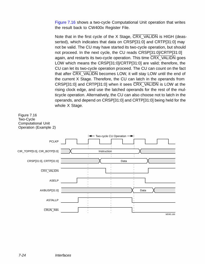
7-24 Interfaces
Figure 7.16 shows a two-cycle Computational Unit operation that writesthe result back to CW400x Register File.
Note that in the first cycle of the X Stage, CRX_VALIDN is HIGH (deas-serted), which indicates that data on CRSP[31:0] and CRTP[31:0] maynot be valid. The CU may have started its two-cycle operation, but shouldnot proceed. In the next cycle, the CU reads CRSP[31:0]/CRTP[31:0]again, and restarts its two-cycle operation. This time CRX_VALIDN goesLOW which means the CRSP[31:0]/CRTP[31:0] are valid; therefore, theCU can let its two-cycle operation proceed. The CU can count on the factthat after CRX_VALIDN becomes LOW, it will stay LOW until the end ofthe current X Stage. Therefore, the CU can latch in the operands fromCRSP[31:0] and CRTP[31:0] when it sees CRX_VALIDN is LOW at therising clock edge, and use the latched operands for the rest of the mul-ticycle operation. Alternatively, the CU can also choose not to latch in theoperands, and depend on CRSP[31:0] and CRTP[31:0] being held for thewhole X Stage.
Figure 7.16Two-CycleComputational UnitOperation (Example 2)
Two-cycle CU Operation
MD95.169
PCLKP
CIR_TOPP[5:0], CIR_BOTP[5:0]
CRSP[31:0], CRTP[31:0]
CRX_VALIDN
ASELP
AXBUSP[31:0]
ASTALLP
CRUN_INN
Instruction
Data
Data

FlexLink Interface 7-25
Figure 7.17 shows a 3-cycle Computational Unit operation whichattempts to write the result back to the CW400x Register File, but is killedby CKILLXP.
Note that during Cycle 3, although ASTALLP is asserted, CRUN_INN isdeasserted. This is because the CW400x ignores the CU data depen-dency stall request when it sees CKILLXP asserted. If the CU wants tostall the CW400x regardless of CKILLXP, it can output a separate stallsignal to the CW400x GOE Module (refer to Section 6.1, “Global OutputEnable Module (GOE)”) which ORs all modules’ stall signals to generatea global stall signal.
Figure 7.17Three-CycleComputational UnitOperation
MD95.170
1 2 3
PCLKP
CIR_TOPP[5:0], CIR_BOTP[5:0]
CRSP[31:0], CRTP[31:0]
CRX_VALIDN
CKILLXP
ASELP
AXBUSP[31:0]
ASTALLP
CRUN_INN
Instruction
Data

7-26 Interfaces
Figure 7.18 shows a two-cycle Computational Unit operation whichattempts to write result back to the CW400x Register File, but is stalledby the CW400x by an extra cycle, and then killed by CKILLXP.
Figure 7.18Stalled Two-CycleComputational UnitOperation
CU Stall CycleCPU Extra
Instruction's X Stage
MD95.171
PCLKP
CIR_TOPP[5:0], CIR_BOTP[5:0]
CRSP[31:0], CRTP[31:0]
CRX_VALIDN
CKILLXP
CRUN_INN
AXBUSP[31:0]
ASELP
ASTALLP
Stall Cycle
Instruction
Data

FlexLink Interface 7-27
7.2.3.3 Multicycle Operation - Result Back to Own Register File
Figure 7.19 shows a two-cycle Computational Unit operation which writesresult back to its own register file.
Figure 7.19Two-Cycle CUOperation withWriteback (Example 1)
MD95.172
CU Writes Result Back to its Own Registers
PCLKP
CIR_TOPP[5:0], CIR_BOTP[5:0]
CRSP[31:0], CRTP[31:0]
CRX_VALIDN
ASELP
AXBUSP[31:0]
ASTALLP
CRUN_INN
CU Instruction Move from CU Instruction
Data
Data
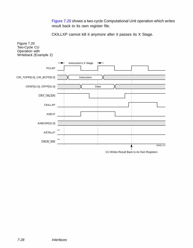
7-28 Interfaces
Figure 7.20 shows a two-cycle Computational Unit operation which writesresult back to its own register file.
CKILLXP cannot kill it anymore after it passes its X Stage.
Figure 7.20Two-Cycle CUOperation withWriteback (Example 2)
CRX_VALIDN
Instruction's X Stage
MD95.173
CU Writes Result Back to its Own Registers
PCLKP
CIR_TOPP[5:0], CIR_BOTP[5:0]
CRSP[31:0], CRTP[31:0]
CKILLXP
ASELP
AXBUSP[31:0]
ASTALLP
CRUN_INN
Instruction
Data

8-1
Chapter 8Methodologies andLayout Guidelines
This chapter describes methodologies and layout guidelines for theCW400x Microprocessor. It contains the following sections:
♦ Section 8.1, “Clocking Methodology”
♦ Section 8.2, “Scan Methodology”
♦ Section 8.3, “Layout Guidelines”
For Data Bus Methodology see Section 6.1, “Global Output Enable Mod-ule (GOE).”
8.1ClockingMethodology
This section describes the clocking methodology used in the CW400xCore, the MMU and the MDU building blocks. Users may consider this aguideline of how they handle the clock when designing their own buildingblocks.

8-2 Methodologies and Layout Guidelines
LSI Logic recommends a two-level clock distribution network for chipswhich use the CW400x (see Figure 8.1).
Figure 8.1Two-level ClockDistribution Network
8.1.1Duty Cycle
The duty cycle of clock oscillators varies in different IC and boarddesigns, and when the global clock passes through the clock tree to localregisters, it goes through cells which have different rising and fallingdelays. As a result, the clock duty cycle may vary from 30% to 70%. Inorder to make them easier to use, the CW400x, MMU, and MDU aredesigned to work with such a varying clock duty cycle by using only oneedge of the clock.
8.1.2Local ClockBuffers
Inside each core or building block, the global clock is buffered locallybefore being used, and the clock buffers are in separate modules(cw400x_gck* modules described Section 8.1.3, “Gated Clocks”) withinthe building blocks. This methodology allows the designer to specify thatthe clock buffer modules not be touched by the synthesis tool, andthereby minimize clock skews and ramp times.
CW400xBuilding
Building
Chip That Includes the CW400x Core
BoardLevelClock
Use wire length to controlthe clock skew betweendifferent blocks on the die;a balanced clock tree cangive a clock skew of lessthan 0.2 ns between buildingblocks in a nominal environment.
Block 2
Block 1

Clocking Methodology 8-3
Table 8.1 shows what driver types and the module names LSI Logic usesfor different loadings.
Table 8.1Driver Type andModule Name
In a nominal environment, the CW400x and MDU has a typical clockdriver delay of 0.7 ns (from the clock input through the local buffers toindividual flip-flops or latches, including the wire delay) while the MMUhas a typical clock driver delay of 0.6 ns. Clock skews are also limited to0.1 ns inside the CW400x, MMU, and MDU.
8.1.3Gated Clocks
The CW400x, the MMU, and the MDU use gated clocks to save power.These building blocks use the cw400x_gckand2x (x= l, a, b, c) gatedclock buffer modules which contain the logic shown in Figure 8.2. Thislogic guarantees the signal which is to be gated with the clock is stableover the high phase of the clock. Having the logic in a separate moduleensures that the synthesis tool does not improperly optimize the logic.
Figure 8.2Gated Clock Logic
8.1.4Delayed Clocks
The CW400x uses delay cells to delay the clocks for the CW400x’s Reg-ister File and in the MDU for latching operands. LSI Logic has manuallychecked the delayed clocks after layout to make sure that the clocks havethe correct timing.
Driver Type Module NameLoad Range(Standard Loads)
and2l cw400x_gckand2l 2.3 - 4.8
and2a cw400x_gckand2a 4.5 - 9.8
and2b cw400x_gckand2b 9.0 - 19.7
and2c cw400x_gckand2c 14.4 - 30.8
Clock
Gated ClockGate SignalGSCAN_ENABLEP Q
Latch
GN
AND2xDOR

8-4 Methodologies and Layout Guidelines
8.1.5Hold TimeMargin
To ensure that the core and building blocks are free of hold time prob-lems, additional hold time margin (see Table 8.2) is guaranteed to allinternal flip-flops. This additional hold time margin ensures a robustdesign that is immune from bad clock skew.
Table 8.2Hold Time Margin
8.2ScanMethodology
Users of the CW400x Core have two options for production testing. Theycan use the core as part of their chip-level full-scan chain or they canuse the core with an Automatic Test Pattern Generation (ATPG) shellaround it and LSI Logic guaranteed patterns.
This section describes how to perform tests for the CW400x using eachof these methods. It is important that the customer follow all LSI Logicmethodology recommendations for scan testing.
For this core, LSI Logic used Mentor Graphics DFT Tools: DFTAdvisorfor scan insertion and rules checking and FastScan for ATPG. For mostcustomers, it would be best to use the same toolset if possible, in orderto avoid any roadblocks associated with using other tools.
Environment Hold Time Margin
BCCOM 0.3 ns
NOM 0.5 ns
WCCOM 0.7 ns

Scan Methodology 8-5
8.2.1Methodology
Figure 8.3 shows the generic flow which should be used for scan inser-tion and ATPG for the core. The diagram numbers each step, which areexplained in the text following the diagram.
Figure 8.3Methodology Flowchart
1. Start.
2. Design - Design includes all aspects of design, including RTL design,Synthesis, Timing Analysis, and so on. Layout is not included in thisflow; it should be done after scan insertion.
3. Synthesize Netlist - Use a preliminary netlist in order to start scaninsertion and ATPG. Remember that any resynthesis will requireredoing the scan insertion and ATPG.
Note that inserting scan will probably increase the area and pathdelays, so layout and final timing analysis must be done after scaninsertion.
4. Rules Checking - Rules checks includes all Design-for-Test ruleschecking. This may include checks from LSI Logic and/or from theATPG Tool itself. LSI Logic supplies a dummy core netlist for runningall rules checks. This netlist should prevent violations from occurring
3. Synthesize Netlist
4. Rules Checking
6. Insert Scan
2. Design
5. Pass
YES
NO
7. Hook up Core
8. Run ATPG
10. End
9. GoodNO
YES
Coverage?
to Layout
Checks?
1. Start

8-6 Methodologies and Layout Guidelines
inside the core. This dummy netlist contains no gates, just IO pins,and a simple connection from scan test input to scan test output.
5. Pass Checks? - If rules checking passes, then insert scan. If rulesare violated, fix them by changing the design.
6. Insert Scan - Perform scan chain synthesis.
7. Hook up Core - Once scan is inserted, manually hook up the coreas needed to the scan chain. The core and all building blocks havefull-scan inserted already.
8. Run ATPG - Either the customer or LSI Logic can run ATPG. (ATPGis described more fully in Sections 8.2.2 through 8.2.6.) LSI Logicgrants access to all building block netlists. LSI Logic runs throughATPG for all modules to make sure that 99% coverage is achievable.LSI Logic does not guarantee fault coverage for building blocks; thecustomer must generate patterns for them.
9. Good Coverage? - If coverage is not good, change the way the ATPGtool is being utilized, change the scan-insertion scheme, or add con-trol and/or observation points. If any of the parts of the design areuntestable, change the design.
10. End - Once all of these aspects are fixed, fault coverage will reachan acceptable level. This level is usually 99% single stuck-at faultcoverage.
8.2.2Regeneration(RecommendedMethodology)
8.2.2.1 Overview
This method uses the scan chain inside of the core as part of the overallscan chain. ATPG patterns are completely regenerated for the core. Theadvantage of this flow is that it saves area and performance associatedwith an ATPG shell which otherwise would need to be placed around thecore. The disadvantage is that the ATPG vectors must be regeneratedfor each customer design. Because of this, LSI Logic cannot guaranteefault coverage inside of the core with this methodology.
With this core, Mentor FastScan must be used for ATPG. This does notprevent the customer from doing preliminary ATPG with a different tool.But, in order to get the highest coverage, the advanced features ofFastScan are needed. Note that we did not use any scan-sequentialpatterns.

Scan Methodology 8-7
8.2.2.2 Methodology
In order to use this flow, the customer must be using full-scan in the logicoutside of the core. When hooking up the core to the scan chain, the cus-tomer can choose to hook everything up into a single chain or multiplechains. As long as the LSI Logic scan methodology is followed, thereshould be no problem.
In order to run preliminary ATPG, the customer must use the dummycore netlist. The customer will not have access to the internal core netlist,and so cannot do ATPG for this block. LSI Logic Field Coreware Engi-neers (FCEs) will generate ATPG patterns using Mentor FastScan.
8.2.3Core ATPGShell
8.2.3.1 Overview
In this method, the customer uses pre-generated core patterns with anATPG shell placed around the core. The advantage of this method is thatthe customer does not need to regenerate core patterns and is guaran-teed greater than 99% coverage for the core. The disadvantages are theadded area and delays associated with the ATPG shell. Also, the corescan test input and scan test output pins must be IO pins of the chip,and so may need special attention.

8-8 Methodologies and Layout Guidelines
8.2.3.2 ATPG Shell
The ATPG shell enables all core inputs to be controllable and all outputsto be observable. During normal operation, it does not affect the func-tionality of the I/Os, but, when GTEST_ENABLEP is asserted, the inputsare driven by scannable flip-flops. The outputs are clocked into scanna-ble flip-flops as well (Figure 8.4 and Figure 8.5). Note that the flip-flop forinputs can be shared with the one for outputs, since inputs only use theQ Pin and outputs only use the D Pin.
Figure 8.4Input PinSchematic forATPG Shell
Figure 8.5Output PinSchematic forATPG Shell
cw400x_ccpu_scan_shell Module
cw400x_ccpu Module
Input Pin
GTEST_ENABLEP
0
1
Input Pin
PCLKP
D Q
cw400x_ccpu_scan_shell Module
cw400x_ccpu Module
Output PinOutput Pin
PCLKP
D Q

Scan Methodology 8-9
Bidirectional I/Os are inherently observable and controllable without addi-tional logic, since they are both inputs and outputs (Figure 8.6). COENshould be asserted during scan testing of the CW400x.
Figure 8.6Bidirectional PinSchematic forATPG Shell
To use the ATPG Shell, the customer calls it instead of the CW400xCore. It has exactly the same I/O pins as the core itself. This modulecalls the core inside of it.
8.2.3.3 Methodology
In order to use this flow, the customer must bring the core scan pins(GSCAN_INP, GSCAN_OUTP, GSCAN_ENABLEP, andGTEST_ENABLEP) out to the chip level. The customer can use any test-ing methodology outside of the core.
The customer can run preliminary ATPG without the core, since it shouldnot impact the outside logic anyway. In this scenario, the customer willhave some test patterns and the core will also have test patterns.
8.2.4CW400x ATPGGuidelines
The CW400x is a special case because it contains a RAM (the RegisterFile). This RAM is isolated by scannable flip-flops, so it should not givetoo much trouble. It does require that a functional pattern be run in orderto test the register file itself. Furthermore, this register file test sequenceis needed to fully test the paths into and out of the register file. TheCW400x logic needs these patterns to get above 99% coverage.
The datapath has scan inserted manually. It uses an optimized scanstructure that takes advantage of existing routes. This saves area, but the
cw400x_ccpu_scan_shell Module
cw400x_ccpu Module
Bidirectional PinPinBidirectional

8-10 Methodologies and Layout Guidelines
control must be such that certain signals are held a certain way duringscan. The control modules have scan inserted by DFTAdvisor.
8.2.5MMU ATPGGuidelines
The MMU must have scan inserted by DFTAdvisor. Be careful to addproper buffering to GSCAN_INP, GSCAN_OUTP, and GSCAN_ENABLEP.
The MMU is connected to the Data Bus, so care must be taken sincethis is a 3-stateable bus. Furthermore, the MMU contains a RAM,RRTLB1. This RAM is not isolated. Since the customer will have to runcertain patterns through this RAM in order to test it, we have countedthese simple patterns in the logic coverage. They are needed to test allpaths to and from the MMU. By doing this, we believe the MMU willachieve greater than 99% coverage. The customer should be able to runATPG on the MMU, although it will just show decreased coverage due tothe RAM being unknown.
8.2.6MDU ATPGGuidelines
In the MDU, the datapath has scan inserted manually in the structuraldesign. The cw400x_amdu_ctrl module must have scan inserted byDFTAdvisor. Then, these two chains must be stitched together.
You must convert the flip-flop that is clocked by the delayed clock to abuffer for the purposes of ATPG. It cannot be scanned because of thedelayed clock, but it will always clock in the value just calculated so thisis functionally equivalent for ATPG.
Be careful to add proper buffering to GSCAN_INP, GSCAN_OUTP, andGSCAN_ENABLEP after scan insertion.
Other than these things, the MDU is straightforward — no RAMs, no3-states. It should get very high coverage.

Layout Guidelines 8-11
8.3LayoutGuidelines
The performance of the CW400x Microprocessor Core, and the easewith which it is laid out, is dependent on the placement of the CW400xand the associated building blocks on the chip. This chapter discussesthe connections between these modules, and gives suggestions as tohow to lay out the CW400x Microprocessor Core and its associatedbuilding blocks.
8.3.1Hardmac I/OPlacement
In order to understand how the modules should be placed relative toeach other, it is important to know the locations of the interfaces on thehardmacs. Three modules are provided as hardmacs: the CW400xMicroprocessor, the BBCC, and the MDU. Although the orientation ofthese hardmacs can be rotated and flipped, this chapter refers to thehardmacs in the orientation shown in Figures 8.7 through 8.9.

8-12 Methodologies and Layout Guidelines
8.3.1.1 CW400x
Figure 8.7 shows a diagram of the CW400x Microprocessor Hardmac.Notice that the Data Bus can be accessed from both the left and rightsides of the hardmac. This layout helps avoid routing the Data Busaround the hardmac. In most cases, only the left Data Bus pins will beused, since this is the side with the control pins.
Figure 8.7CW400x Hardmac
Interrupts
CoprocessorCondition Bits
Data OutputEnable
MMUExceptions
CBusControls
CUInstructionBus
Data Bus (DATAP[31:0])
Address (ADDRP[31:0])CU Register File Buses/CU Result Bus/
MD95.155
CW400x

Layout Guidelines 8-13
8.3.1.2 BBCC
Figure 8.8 shows a diagram of the BBCC Hardmac. This hardmac alsohas pins for the Data Bus on both sides of the hardmac in order toimprove the routing of the Data Bus.
Figure 8.8BBCC Hardmac B-Bus Address B-Bus Data
CBusControls
B-BusControls
ConfigurationRegister
Cache RAMControls
TagTag for Matching
IndexData Bus (DATAP[31:0])
DataOutputEnable
Mapped Address
Address
WBControl WB Address WB Data
MD95.156
BBCC
(MADDROUTP[31:2])
(ADDRP[14:2]
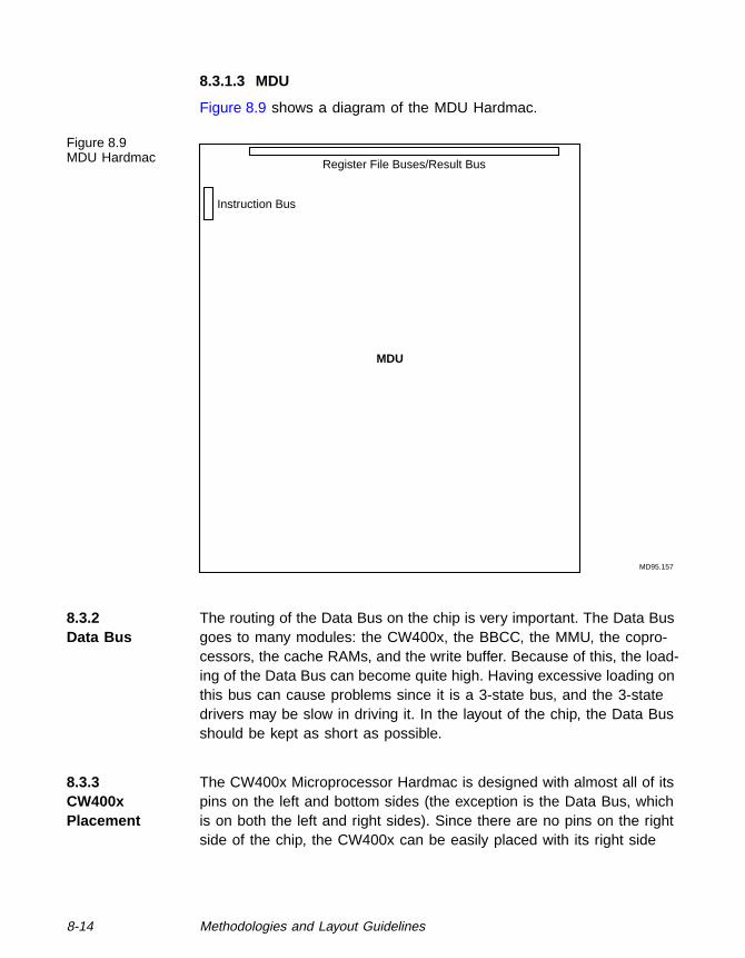
8-14 Methodologies and Layout Guidelines
8.3.1.3 MDU
Figure 8.9 shows a diagram of the MDU Hardmac.
Figure 8.9MDU Hardmac
8.3.2Data Bus
The routing of the Data Bus on the chip is very important. The Data Busgoes to many modules: the CW400x, the BBCC, the MMU, the copro-cessors, the cache RAMs, and the write buffer. Because of this, the load-ing of the Data Bus can become quite high. Having excessive loading onthis bus can cause problems since it is a 3-state bus, and the 3-statedrivers may be slow in driving it. In the layout of the chip, the Data Busshould be kept as short as possible.
8.3.3CW400xPlacement
The CW400x Microprocessor Hardmac is designed with almost all of itspins on the left and bottom sides (the exception is the Data Bus, whichis on both the left and right sides). Since there are no pins on the rightside of the chip, the CW400x can be easily placed with its right side
Register File Buses/Result Bus
Instruction Bus
MDU
MD95.157

Layout Guidelines 8-15
against the edge of the chip (shown as (a) in Figure 8.10). The top of theCW400x can also be placed against an edge of the chip (placing theCW400x in a corner, which is shown as (b)). The bottom of the CW400xcan be placed near an edge of the chip if the design does not containan MMU or Computational Unit (CU) (shown as (c)).
Figure 8.10CW400x PlacementExample
Chip ChipChip with no
CW400x
(a) (b) (c)MD95.158
MMU or CU
CW400x
CW400x

8-16 Methodologies and Layout Guidelines
8.3.4BBCCPlacement
The BBCC is designed to be placed very close to the CW400x, on its leftside, as shown in the following figure. The Data Bus pins of the CW400xand the BBCC should be exactly aligned in order to obtain the best rout-ing of the Data Bus. Aligning the Data Bus pins causes the power busesin the CW400x and BBCC to also align.
While the CW400x and BBCC should be placed close together, enoughroom should be left for the signals that need to be routed between theCW400x and the BBCC. These signals include the MMU Exception Sig-nals (if a MMU is in the design), and the CU Instruction Bus (if a CU isin the design). The Data Bus may also need to be routed between theCW400x and the BBCC in some instances. Figure 8.11 shows BBCCsuggested placement.
Figure 8.11BBCC SuggestedPlacement
Data Bus
Power
CBusControlsCBus
Controls
CW400x
BBCC
MD95.159

Layout Guidelines 8-17
8.3.5ComputationalUnit Placement
The Computational Unit module (for example the MDU Building Block)should be placed below the CW400x, as shown in Figure 8.12.
Figure 8.12Computational UnitSuggestedPlacement
CU Instruction Bus
CU Register File Buses/CU Result Bus
Instruction
Register File Buses/Result Bus
CW400x
MDU
Bus
MD95.160

8-18 Methodologies and Layout Guidelines
8.3.6MMU Placement
The MMU Building Block may consist of an MMU or the MMU Stub. It isnot a hardmac. The MMU should also be placed below the CW400x (asshown in Figure 8.13). If both a CU and a real MMU exist in the design,then the layout should accommodate both as well as possible. Mostlikely, placing the MMU to the left of the CU would result in better routing(as shown in Figure 8.14).
Figure 8.13MMU (with no CU)SuggestedPlacement
MMU Exceptions
ADDRP[31:0]
MADDROUTP[31:2]
ADDRP[14:2]
BBCC
CW400x
MMU
MD95.161-1

Layout Guidelines 8-19
Figure 8.14MMU (with CU)SuggestedPlacement
MMU Exceptions
MADDROUTP[31:2]
ADDRP[14:2]
BBCC
CW400x
MMU
MD95.161-2
Instruction
Register File BusesResult Bus
CU
Address
Register File/Results
ADDRP[31:0]/CU Register File Buses/
CU Results
CU Instruction Bus
Bus

8-20 Methodologies and Layout Guidelines
8.3.7CoprocessorPlacement
The interface between a coprocessor and the CW400x consists of theData Bus and the CBus controls. The coprocessor can be placed to theleft of the CW400x if no BBCC is present in the design. If a BBCC doesexist in the design, the coprocessor can be placed either above or belowthe BBCC. Some examples of coprocessor placement are shown in Fig-ures 8.15 through 8.17.
Figure 8.15CoprocessorPlacementExample 1
Figure 8.16CoprocessorPlacementExample 2
CBusControls
CW400x
MD95.162-1
Coprocessor Data Bus
CBusControls
CW400x
MD95.162-2
Coprocessor
CBusControls
BBCC
Data Bus
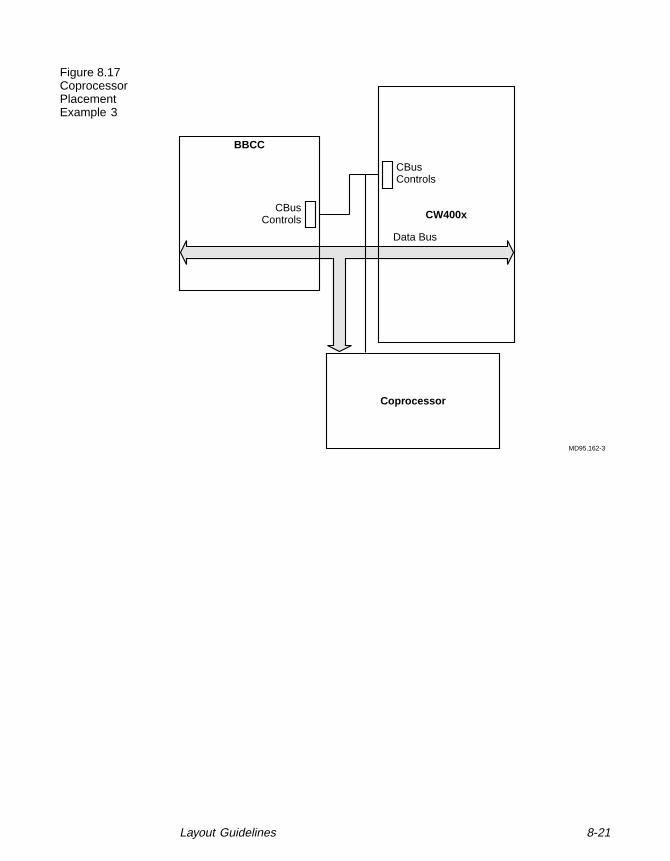
Layout Guidelines 8-21
Figure 8.17CoprocessorPlacementExample 3
CBusControls
CW400x
MD95.162-3
Coprocessor
CBusControls
BBCC
Data Bus

8-22 Methodologies and Layout Guidelines
8.3.8Global OutputEnable (GOE)Placement
The Global Output Enable (GOE) is a small module, and is not providedas a hardmac. It generates the Run Signals, and also the output enablesfor the Data Bus. These are both time-critical, and the placement of theGOE is important. It should be close to the CW400x, BBCC, MMU, CU,and coprocessors. A suggested placement for the GOE is shown inFigure 8.18. The GOE is described in more detail in Chapter 6.
Figure 8.18Global OutputEnable SuggestedPlacement
BBCC
CW400x
MD95.163
MMU, CU,
Output Enable (MOEN)GOE
orCoprocessor
Run Signals
Run Signals
Output Enable (COEN)
Run Signals
Output Enable(BIUOEN)

Layout Guidelines 8-23
8.3.9Cache RAMsPlacement
The Cache RAMs are controlled by the BBCC. The control pins are onthe left side of the BBCC. It is more important to have the Tag RAMsclose to the BBCC control pins than the Data RAMs, since the tagmatch(the match logic between the tag in the Tag RAMs and the tag from theBBCC) is a critical path and should be optimized. An example placementof the cache RAMs is shown in Figure 8.19.
Figure 8.19Cache RAMsPlacement Example
BBCC
CW400x
MD95.164
Cache RAM Controls
Tag
D-Cache/I-CacheSet 0
Tag RAM
I-Cache Set 1Tag RAM
I-Cache Set 1Data RAM
D-Cache/I-CacheSet 0
Data RAM
Data Bus

8-24 Methodologies and Layout Guidelines
8.3.10TagmatchPlacement
The logic to compare the tags in the tag RAMs to the transaction tagshould be close to both the tag RAMs and the BBCC, as this logic istime-critical. The tag RAMs’ output is also connected to the Data Busthrough 3-state gates. Figure 8.20 shows the connections to the tag-match logic and the connections from the tag RAMs to the Data Bus.
Figure 8.20Tagmatch Placement
BBCC CW400x
MD95.174
Match
Tag for Matching
D-Cache/I-CacheSet 0
Tag RAM
I-Cache Set 1Tag RAM
I-Cache Set 1Data RAM
D-Cache/I-CacheSet 0
Data RAM
TAG Match/3-State Gates
Data Bus

Layout Guidelines 8-25
8.3.11Write BufferPlacement
The Write Buffer has many connections to the bottom of the BBCC. Italso receives data from the Data Bus and the address from the MMU.Figure 8.21 shows an example placement.
Figure 8.21Write BufferPlacementExample
CW400x
BBCC
MD95.175
WB WB
Write Buffer
MMU
MADDROUTP[31:2]
Address
Data Bus
Address Data

8-26 Methodologies and Layout Guidelines
8.3.12B-Bus DevicePlacement
B-Bus Devices have many connections to the top of the BBCC. An exam-ple placement is shown in Figure 8.22.
Figure 8.22B-Bus DevicePlacementExample
CW400x
BBCC
MD95.176
B-Bus B-BusAddress Data
B-BusControls
B-Bus Device
Data Bus

A-1
Appendix AStructural ALUImproper UnknownValue (X) Handling
The structural simulation model for the CW400x does not handleunknown values (Xs) properly in four instructions. The actual siliconworks correctly, but the simulation model is incorrect. It is incorrectbecause of LSI Logic’s fast implementation of the ALU, and cannot befixed while keeping accurate gate-level modeling of the design.
The four instructions are:
1. AND rd, rs, rt
rd is the destination register
rs is a source register which contains an X at bit b (b is any bit)
rt is a source register which contains a zero at bit b
After execution of the AND Instruction, the destination register willincorrectly contain an X instead of a zero at bit b.
example: rs = 0x0000.000X; rt = 0x0000.0000; rd = 0x0000.000X
2. ANDI rt, rs, immed
rt is the destination register
rs is a source register which contains an X at bit b (b is any bit)
immed is the immediate field which contains a zero at bit b
After execution of the ANDI Instruction, the destination register willincorrectly contain an X instead of a zero at bit b.
example: rs = 0x0000.00X0; immed = 0x0000.0000; rt =0x0000.00X0
3. OR rd, rs, rt
rd is the destination register
rs is a source register which contains an X at bit b (b is any bit)
rt is a source register which contains a one at bit b

A-2 Structural ALU Improper Unknown Value (X) Handling
After execution of the OR Instruction, the destination register willincorrectly contain an X instead of a one at bit b.
Switching rs and rt will produce an identical incorrect X result.
example: rs = 0x0000.000X; rt = 0x0000.0001; rd = 0x0000.000X
example: rs = 0x0000.0001; rt = 0x0000.000X; rd = 0x0000.000X
4. ORI rt, rs, immed
rt is the destination register
rs is a source register which contains an X at bit b (b is any bit)
immed is the immediate field which contains a one at bit b
After execution of the ORI Instruction, the destination register willincorrectly contain an X instead of a one at bit b.
Switching rs and immed will produce an identical incorrect X result.
example: rs = 0x0000.00X0; immed = 0x0000.0010; rt =0x0000.00X0
example: rs = 0x0000.0010; immed = 0x0000.00X0; rt =0x0000.00X0
All remaining cases, including X cases, are handled correctly.
The incorrect X handling may create problems when trying to mask reg-isters that have not been fully initialized. Specifically, the CP0 Cause andStatus Registers should be initialized in the software reset handler to pre-vent this problem.
Note that AND rd, r0, X and ANDI rt, r0, X properly produce a 0and may be used to mask uninitialized registers.
The Register Transfer Level (RTL) ALU handles all cases, including thefour listed above, correctly.

Customer Feedback
We would appreciate your feedback on this document. Please copy thefollowing page, add your comments, and fax it to us at the address onthe following page.
If appropriate, please also fax copies of any marked-up pages from thisdocument.
Important: Please include your name, phone number, fax number, andcompany address so that we may contact you directly forclarification or additional information.
Thank you for your help in improving the quality of our documents.

Customer Feedback
Reader’sComments
Fax your comments to:
LSI Logic CorporationTechnical PublicationsM/S G-712Fax: 408.433.8989
Please tell us how you rate this document: MiniRisc CW400x Micropro-cessor Core Technical Manual. Place a check mark in the appropriateblank for each category.
What could we do to improve this document?
If you found errors in this document, please specify the error and pagenumber. If appropriate, please fax a marked-up copy of the page(s).
Please complete the information below so that we may contact youdirectly for clarification or additional information.
Excellent Good Average Fair PoorCompleteness of information ____ ____ ____ ____ ____Clarity of information ____ ____ ____ ____ ____Ease of finding information ____ ____ ____ ____ ____Technical content ____ ____ ____ ____ ____Usefulness of examples andillustrations ____ ____ ____ ____ ____
Overall manual ____ ____ ____ ____ ____
Name Date
Telephone
Title
Company Name
Street
City, State, Zip
Department Mail Stop
Fax

U.S. Distributorsby State
AlabamaHuntsvilleHamilton HallmarkTel: 800.633.2918
Wyle ElectronicsTel: 800.964.9953
ArizonaPhoenixHamilton HallmarkTel: 800.528.8471
Wyle ElectronicsTel: 602.804.7000
TempeHamilton HallmarkTel: 602.414.7705
CaliforniaCulver CityHamilton HallmarkTel: 310.558.2000
IrvineHamilton HallmarkTel: 714.789.4100
♦Wyle ElectronicsTel: 714.789.9953
Los AngelesWyle ElectronicsTel: 818.880.9000
RocklinHamilton HallmarkTel: 916.624.9781
SacramentoWyle ElectronicsTel: 916.638.5282
San DiegoHamilton HallmarkTel: 619.571.7540
Wyle ElectronicsTel: 619.565.9171
San Jose♦Hamilton Hallmark
Tel: 408.435.3500
Santa ClaraWyle ElectronicsTel: 408.727.2500
Woodland HillsHamilton HallmarkTel: 818.594.0404
ColoradoColorado SpringsHamilton HallmarkTel: 719.637.0055
Denver♦Wyle Electronics
Tel: 303.457.9953
EnglewoodHamilton HallmarkTel: 303.790.1662
ConnecticutCheshireHamilton HallmarkTel: 203.271.2844
FloridaFort LauderdaleHamilton HallmarkTel: 305.484.5482
Wyle ElectronicsTel: 305.420.0500
LargoHamilton HallmarkTel: 800.282.9350
OrlandoWyle ElectronicsTel: 407.740.7450
Tampa/N. FloridaWyle ElectronicsTel: 800.395.9953
Winter ParkHamilton HallmarkTel: 407.657.3317
GeorgiaAtlantaWyle ElectronicsTel: 800.876.9953
DuluthHamilton HallmarkTel: 800.241.8182
IllinoisArlington Heights
♦Hamilton HallmarkTel: 708.797.7300
ChicagoWyle ElectronicsTel: 708.620.0969
IowaCarmelHamilton HallmarkTel: 800.829.0146
KansasOverland ParkHamilton HallmarkTel: 800.332.4375
KentuckyLexingtonHamilton HallmarkTel: 800.235.6039
MarylandBaltimoreWyle ElectronicsTel: 410.312.4844
ColumbiaHamilton HallmarkTel: 800.638.5988
MassachusettsBoston
♦Wyle ElectronicsTel: 800.444.9953
Peabody♦Hamilton Hallmark
Tel: 508.532.3701
MichiganPlymouthHamilton HallmarkTel: 313.416.5800
MinnesotaBloomingtonHamilton HallmarkTel: 612.881.2600
MinneapolisWyle ElectronicsTel: 800.860.9953
MissouriEarth CityHamilton HallmarkTel: 314.291.5350
New JerseyMt. LaurelHamilton HallmarkTel: 609.222.6400
No. New JerseyWyle ElectronicsTel: 201.882.8358
ParsippanyHamilton HallmarkTel: 201.515.1641
New MexicoAlburquerqueHamilton HallmarkTel: 505293.5119
New YorkHauppaugeHamilton HallmarkTel: 516.737.7400
Long IslandWyle ElectronicsTel: 516.293.8446
RochesterHamilton HallmarkTel: 800.462.6440
North CarolinaRaleighHamilton HallmarkTel: 919.872.0712
Wyle ElectronicsTel: 919.469.1502
OhioClevelandWyle ElectronicsTel: 216.248.9996
DaytonHamilton HallmarkTel: 800.423.4688
Wyle ElectronicsTel: 513.436.9953
SolonHamilton HallmarkTel: 216.498.1100
ToledoWyle ElectronicsTel: 419.861.2622
WorthingtonHamilton HallmarkTel: 614.888.3313
OklahomaTulsaHamilton HallmarkTel: 918.254.6110
OregonBeavertonHamilton HallmarkTel: 503.526.6200
PortlandWyle ElectronicsTel: 503.643.7900
PennsylvaniaPhiladelphiaWyle ElectronicsTel: 800.871.9953
TexasAustinHamilton HallmarkTel: 512.258.8848
Wyle ElectronicsTel: 800.365.9953
DallasHamilton HallmarkTel: 214.553.4302
Wyle ElectronicsTel: 800.955.9953
HoustonHamilton HallmarkTel: 713.787.8300
Wyle ElectronicsTel: 713.784.9953
San AntonioWyle ElectronicsTel: 210.697.2816
UtahSalt Lake CityHamilton HallmarkTel: 801.266.2022
Wyle ElectronicsTel: 801.974.9953
WashingtonRedmondHamilton HallmarkTel: 206.881.6697
SeattleWyle ElectronicsTel: 800.248.9953
WisconsinMilwaukeeWyle ElectronicsTel: 800.867.9953
New BerlinHamilton HallmarkTel: 414.780.7200
♦Dstributors withDesign ResourceCenters

Sales Offices and DesignResource Centers
Printed in USA1096.500.G
Printed onRecycled Paper
ISO 9000 Certified
New JerseyEdison
♦Tel: 908.549.4500Fax: 908.549.4802
New YorkNew YorkTel: 716.223.8820Fax: 716.223.8822
North CarolinaRaleighTel: 919.783.8833Fax: 919.783.8909
OregonBeavertonTel: 503.645.0589Fax: 503.645.6612
TexasAustinTel: 512.388.7294Fax: 512.388.4171
Dallas♦Tel: 214.788.2966
Fax: 214.233.9234
HoustonTel: 713.379.7800Fax: 713.379.7818
WashingtonBellevueTel: 206.822.4384Fax: 206.827.2884
INTERNATIONAL
AustraliaReptechnic Pty LtdNew South WalesTel: 612.9953.9844Fax: 612.9953.9683
CanadaLSI Logic Corporation ofCanada IncOntarioOttawa
♦Tel: 613.592.1263Fax: 613.592.3253
Toronto♦Tel: 416.620.7400
Fax: 416.620.5005
QuebecPointe Claire
♦Tel: 514.694.2417Fax: 514.694.2699
LSI Logic CorporationCorporate HeadquartersTel: 408.433.8000Fax: 408.433.8989
UNITED STATES
CaliforniaIrvine
♦Tel: 714.553.5600Fax: 714.474.8101
San DiegoTel: 619.635.1300Fax: 619.635.1350
Silicon ValleySales OfficeTel: 408.433.8000Fax: 408.433.7783Design Center
♦Tel: 408.433.8000Fax: 408.433.2820
ColoradoBoulderTel: 303.447.3800Fax: 303.541.0641
FloridaBoca RatonTel: 407.989.3236Fax: 407.989.3237
GeorgiaAtlantaTel: 770.395.3800Fax: 770.395.3811
IllinoisSchaumburg
♦Tel: 847.995.1600Fax: 847.995.1622
KentuckyBowling GreenTel: 502.793.0010Fax: 502.793.0040
MarylandBethesda
♦Tel: 301.897.5800Fax: 301.897.8389
MassachusettsWaltham
♦Tel: 617.890.0180Fax: 617.890.6158
MinnesotaMinneapolis
♦Tel: 612.921.8300Fax: 612.921.8399
DenmarkLSI Logic DevelopmentCentreBallerupTel: 45.44.86.55.55Fax: 45.44.86.55.56
FranceLSI Logic S.A.Paris
♦Tel: 33.1.34.63.13.13Fax: 33.1.34.63.13.19
GermanyLSI Logic GmbHMunich
♦Tel: 49.89.4.58.33.0Fax: 49.89.4.58.33.108
StuttgartTel: 49.711.13.96.90Fax: 49.711.86.61.428
Hong KongAVT Industrial LtdHong KongTel: 852.2428.00008Fax: 852.2401.2105
IndiaLogiCAD India Private LtdBangaloreTel: 91.80.526.2500Fax: 91.80.338.6591
IsraelLSI LogicRamat Hasharon
♦Tel: 972.3.5.403741Fax: 972.3.5.403747
Netanya♦Tel: 972.9.657190
Fax: 972.9.657194
ItalyLSI Logic S.P.A.Milano
♦Tel: 39.39.687371Fax: 39.39.6057867
JapanLSI Logic K.K.Tokyo
♦Tel: 81.3.5463.7821Fax: 81.3.5463.7820
Osaka♦Tel: 81.6.947.5281
Fax: 81.6.947.5287
KoreaLSI Logic Corporation ofKorea LtdSeoul
♦Tel: 82.2.561.2921Fax: 82.2.554.9327
SingaporeDesner Electronics Pte LtdSingaporeTel: 65.285.1566Fax: 65.284.9466
Electronic Resources LtdTel: 65.298.0888Fax: 65.298.1111
SpainLSI Logic S.A.Madrid
♦Tel: 34.1.3672200Fax: 34.1.3673151
SwedenLSI Logic ABStockholm
♦Tel: 46.8.444.15.00Fax: 46.8.750.66.47
SwitzerlandLSI Logic Sulzer AGBrugg/BielTel: 41.32.536363Fax: 41.32.536367
TaiwanLSI Logic Asia-PacificRegional OfficeTaipei
♦Tel: 886.2.718.7828Fax: 886.2.718.8869
Jeilin TechnologyCorporationTel: 886.2.248.4828Fax: 886.2.248.9765
United KingdomLSI Logic Europe plcBracknell
♦Tel: 44.1344.426544Fax: 44.1344.481039
♦Sales Offices withDesign Resource Centers