Embed Size (px)
Citation preview
1
MikroMasch® SPM Probes & Test Structures
www.spmtips.com
MikroMasch® Distributor
MikroMasch® is a trademark of NanoWorld AG operated by ISB Ltd.
MikroMasch® HeadquartersInnovative Solutions Bulgaria Ltd.
48 Joliot Curie St.1113 Sofia, Bulgaria
phone: +359 2 865-8629fax: +359 2 [email protected]
MikroMasch® USANanoAndMore USA Corp.
21 Brennan Street, Suite 10Watsonville, CA 95076, USA
Toll Free (US): +1 866 SPMTIPS (776-8477)phone: +1 831-536-5970
fax: +1 [email protected]
MikroMasch® EuropeNanoAndMore GmbH
Spilburg Bld. A1,Steinbühlstrasse 7D-35578 Wetzlar,
Germanyphone: +49 (0) 6441 2003561
fax: +49 (0) 6441 [email protected]
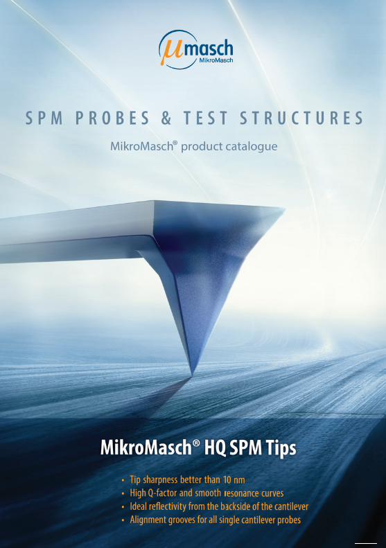
Radius of CuRvatuRe
The radius of curvature measures the sharpness of a particular probe. Typically, the sharper the curvature radius the more fragile a silicon tip is. Conversely, a larger curvature radius provides greater durability, but reduces the benefits of a sharper tip.
Achieving a consistent balance delivers reliable and accurate results. 94% of HQ probes have a radius of curvature between 7 and 10 nm.
tiP sHaPe faCtoRA higher value indicates a higher aspect ratio probe. A tighter range of values indicates a more consistent tip shape.
Results of the tip shape factor tests show consistent and close grouping of data. Known tip shape insures accuracy of results. 92% of HQ probes have an aspect ratio between 1.4 and 1.8.
ResoNaNCe fReQueNCY
Probes are designed to maintain a tight range of resonance frequencies. Reliability in cantilever specifications ensures dependable measurement results.
HQ Probes
Silicon Nitride Probes
The HQ Line (High Quality Line) is MikroMasch well-established state-of-the-art manufacturing and quality control technology. HQ probes are distinguished by their high quality and repeatability of characteristics. In particular, the probes have very consistent tip shape and radius, cantilever stiffness and resonance frequency, and laser reflectivity even for uncoated cantilevers.
We are happy to announce the introduction of MikroMasch Silicon Nitride XNC12 series* of AFM probes. These probes are intended for contact mode measurements on biological and other soft matter specimen. The main features of the back side gold coated XNC12/Cr-Au BS and the overall gold coated XNC12/Cr-Au models are as follows:
• 2 triangular silicon nitride cantilevers with 0.08 N/ m and 0.32 N/m on each side of the holder chip
• Square pyramid silicon nitride tips with typical radii 10 nm (uncoated) and 30 nm (gold coated)
• Chip size 3.4 * 1.6 * 0.5 mm
We always listen to our customers and make sure to provide you with want you need for your AFM research. The XNC12 probes are now available for sale through all our distribution channels.
* See specifications on page 15
< 7 nm
7 to 10 nm
> 10 nm 5%
94%1%
*for all standard, uncoated tips
< 1.4
1.4 to 1.8
> 1.8
2%92%
6%
*for all standard, uncoated tips
< 320 kHz
320 to 380 kHz
380 to 400 kHz
2%93%
5%
*NSC15 Probes
NEW
5
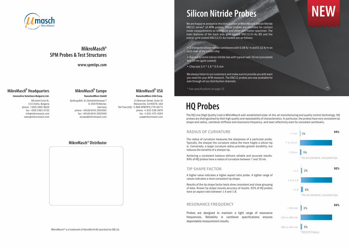
The New HQ Line & Test StructuresProbe chip specifications . . . . . . . . . . . . . . . . . . . . . . . . . 5
REgULARNoncontact and Contact silicon probes . . . . . . . . . . . . . . . . 6
HigH RESoLUTioNHi’Res-C: High Resolution silicon probes . . . . . . . . . . . . . . . . 8
LoNg ScANNiNg / LifETiMEHardened DLC coated silicon probes . . . . . . . . . . . . . . . . . . 9
coNDUcTivEConductive Noncontact and Contact silicon probes . . . . . . . . 10
DPER: High Resolution Conductive silicon probes. . . . . . . . . . 12DPE: Low Noise Conductive silicon probes . . . . . . . . . . . . . . 13
MAgNETicMagnetic Noncontact silicon probes . . . . . . . . . . . . . . . . . 14
SiLicoN NiTRiDE PRobES Silicone Nitride SPM Probes . . . . . . . . . . . . . . . . . . . . . . 15
TiPLESSNoncontact and Contact Tipless silicon probes . . . . . . . . . . . 16
Mix & MATcHMix&Match . . . . . . . . . . . . . . . . . . . . . . . . . . . . . . . . 17
TEST STRUcTURESTGXYZ Series Calibration standards . . . . . . . . . . . . . . . . . 18
TGX Series Calibration standards . . . . . . . . . . . . . . . . . . . 18
TGF11 Series Calibration standards . . . . . . . . . . . . . . . . . . 19PA Series Calibration standards . . . . . . . . . . . . . . . . . . . . 19HOPG. . . . . . . . . . . . . . . . . . . . . . . . . . . . . . . . . . . . 20
REcoMMENDATioNS
Recommendations for specific applications . . . . . . . . . . . . . 22
Co N t e N t P R o b e C H i P s P e C i f i C at i o N s
HQ:NSc/cSc 1 - lever
Cantilever material . . . . . . . . . . . . . . . n-type siliconTip shape . . . . . . . . . . . . . . . . . . . . . . . . pyramidalTip height . . . . . . . . . . . . . . . . . . . . . . . 12 - 18 µmAlignment grooves on the back side of the chip
Series: 14, 15, 16, 17, 18, 19
Series: NSC 35, NSC 36, CSC 37, CSC 38
Series: XNC 12
HQ:NSc/cSc 3 - lever
xNc12 4 - lever
Cantilever material . . . . . . . . . . . . . . . n-type silicon Tip shape . . . . . . . . . . . . . . . . . . . . . . . . pyramidalTip height . . . . . . . . . . . . . . . . . . . . . . . 12 - 18 µm
Cantilever material . . . . . . . . . . . . . . . silicon nitride Tip shape . . . . . . . . . . . . . . . . . . . . . . . . pyramidalTip height . . . . . . . . . . . . . . . . . . . . . . . . . 3.5 µm
Series:NSC 35, NSC 36, CSC 37, CSC 38 Tipless
Series: XSC11
HQ:xSc 4 - lever
Cantilever material . . . . . . . . . . . . . . . n-type silicon Tip shape . . . . . . . . . . . . . . . . . . . . . . . .pyramidalTip height . . . . . . . . . . . . . . . . . . . . . . . 12 - 18 µm
HQ: NSc/cSc Tipless 3 - lever
Cantilever material . . . . . . . . . . . . . . . n-type silicon
6 7
Width
w, ± 3 µm
25
30
37.5
50
27.5
22.5
35
35
35
32.5
32.5
32.5
35
35
35
32.5
32.5
32.5
30
30
30
50
Thickness
± 0.5 µm
2.1
4.0
7.0
2.0
3.0
1.0
2.0
2.0
2.0
1.0
1.0
1.0
2.0
2.0
2.0
1.0
1.0
1.0
2.7
2.7
2.7
2.7
(typical)
160
325
190
13
75
65
205
300
150
90
130
65
40
20
30
20
10
14
15
80
155
350
(typical)
5.0
40
45
0.18
2.8
0.5
8.9
16
5.4
1.0
2
0.6
0.8
0.3
0.4
0.09
0.03
0.05
0.2
2.7
7
42
(range)
110 - 220
265 - 410
170 - 210
10 - 17
60 - 90
25 - 120
130 - 290
185 - 430
95 - 205
30 - 160
45 - 240
25 - 115
30 - 55
15 - 30
20 - 40
8 - 32
5 - 17
6 - 23
12 - 18
60 - 100
115 - 200
250 - 465
(range)
1.8 - 13
20 - 80
30 - 70
0.06 - 0.40
1.2 - 5.5
0.05 - 2.3
2.7 - 24
4.8 - 44
1.7 - 14
0.1 - 4.6
0.2 - 9
0.06 - 2.7
0.3 - 2
0.1 - 0.6
0.1 - 1
0.01 - 0.36
0.003 - 0.13
0.005 - 0.21
0.1 - 0.4
1.1 - 5.6
3 - 16
17 - 90
Resonance Frequency
kHz
Force Constant
N/m
Length
l, ± 5 µm
125
125
225
450
225
125
110
90
130
110
90
130
250
350
300
250
350
300
500
210
150
100
Pyramidal silicon etched probes* are characterized by high tip sharpness and narrow resonance peaks, making them very suitable for topography imaging in dynamic AFM modes and compositional mapping. These probes are available in a wide range of resonance frequencies and spring constants.
HQ: NSc, cSc & xScNoncontact (NSc), contact (cSc) and 4 - Lever (xSc) silicon probes
SEM image of the regular silicon tip
100 nm
R e G u l a R
Tip properties:Tip radius . . . . . . . . . . . . . . . . . ~ 8 nmTip material . . . . . . . . . . . . . . . . . silicon
Back side coating:Al BS. . . . . . . . . . . . . . . . . . . Al 30 nmno Al . . . . . . . . . . . . . . . . . . . . . . noneCr-Au BS . . Au 30 nm on Cr 20 nm sublayer
aPPliCatioN
Phase imaging is among the AFM techniques that can be used to determine nanoscale differences in the properties of a heterogeneous system or of samples with inherent heterogeneity. Phase contrast is dependent on interactions between the tip and the sample, but those interactions are in turn partially dependent on the scan parameters and whether the image is being taken in an attractive or repulsive mode. O’Dea and Burrato used phase imaging to map the proton-conducting domains of a Nafion membrane. They found that the specific interaction forces between the tip and the sample significantly affected the resolution of the proton conducting domains. Imaging in a repulsive regime resulted in an overestimation of the area of the domains and an underestimation in the number of domains. Imaging in an attractive regime resulted in the most accurate phase imaging of the aqueous and fluorocarbon domains of the membrane. When the feedback loop was not optimized or the cantilever was driven above resonance, the phase corresponded with changes in topography rather than changes in the composition of the sample.
In figures (a) and (b) the phase data from repulsive and attractive regimes, respectively, have been overlaid on the corresponding topography image. Features of the phase contrast in the repulsive regime correspond to some features in the topography, while the phase contrast in the attractive regime is independent of the topography. Images were taken with the NSC15/Al BS (now upgraded to HQ:NSC15/Al BS). (O’Dea, J.R. and Burrato, S.K.; J. Phys. Chem. B 2011, 115, 1014-1020.)
0.5 µm
a
b
0.5 µm
HQ: * SC * / * - *
type
series
quantity*
coating
PART NUMbER
* See specifications on page 5
* Please refer to our price list for available package sizes.
N, C, X
11, 14, 15, 16, 17, 18, 19, 35, 36, 37, 38
15, 50, 100, 200, 400
/No Al, /Al BS, /Cr-Au BS
Cantilever
Series
HQ:NSC14
HQ:NSC15
HQ:NSC16
HQ:CSC17
HQ:NSC18
HQ:NSC19**
HQ:NSC35
lever A
lever B
lever C
HQ:NSC36
lever A
lever B
lever C
HQ:CSC37
lever A
lever B
lever C
HQ:CSC38
lever A
lever B
lever C
HQ:XSC11
lever A
lever B
lever C
lever D
AvailableCoatings
/No Al, /Al BS
/No Al, /Al BS, /Cr-Au BS
/No Al, /Al BS
/No Al, /Al BS
/No Al, /Al BS, /Cr-Au BS
/No Al, /Al BS
/No Al, /Al BS, /Cr-Au BS
/No Al, /Al BS, /Cr-Au BS
/No Al, /Al BS
/No Al, /Al BS
/No Al, /Al BS
**ScanAsyst® compatible - ScanAsyst® is a trade mark of Bruker Corp.
8 9
Width
w, ± 3 µm
25
30
27.5
22.5
Thickness
± 0.5 µm
2.1
4.0
3.0
1.0
(typical)
160
325
75
65
(typical)
5.0
40
2.8
0.5
(range)
110 - 220
265 - 410
60 - 90
25 - 120
(range)
1.8 - 13
20 - 80
1.2 - 5.5
0.05 - 2.3
Resonance Frequency
kHz
Force Constant
N/m
AvailableCoatings
/Cr-Au
/Cr-Au
/Cr-Au
/Cr-Au
Length
l, ± 5 µm
125
125
225
125
Cantilever
Series
Hi’Res-C14
Hi’Res-C15
Hi’Res-C18
Hi’Res-C19**
* See specifications on page 5
The Hi’Res-C probes* suffer less contamination than silicon probes and are capable of obtaining many high-resolution scans, although they do require special care in use. Due to the small tip curvature radius, the tip-sample attraction force is minimized.
Advantages of Hi’Res-C are noticeable when scanning small areas (< 250 nm) and flat samples (R
a < 20 nm). On larger images, the resolution is similar to that of General Purpose probes.
Hi’Res-c High Resolution silicon probes
100 nm
H i G H R e s o lu t i o N
SEM image of the Hi’Res-C spike
aPPliCatioN
The advantages of the Hi’Res-C probes are noticeable on scans less than 250 nm in size. The tip radius of 1 nm allows high resolution imaging of nanometer-sized objects like single molecules, ultrathin films, and porous materials in air.
(a) Height image of polydiacetylene crystal obtained with Dimension 5000 SPM microscope and Hi’Res-C probe. Scan size 15 nm. A single defect in the molecular lattice of PDA crystal is visible. (b) Height image of PDA crystal obtained with Agilent 5500 SPM microscope and Hi’Res-C14 probe. Scan size 23 nm. Molecular lattice of PDA is observed only.Images courtesy of Dr. S. Magonov, Agilent Technologies.
8 nm5 nm
a b
Hi’Res - C * / Cr-Au - *PART NUMbERseries
quantity
14, 15, 19
5
Spike radius . . . . . . . . . . . . . . . < 1 nmSpike height . . . . . . . . . . . .100 - 200 nmSpike material . . . . . . . . . . . diamond-like
Overall coating:Au overall coating . . . . . . . . . . . . 30 nmCr overall sublayer . . . . . . . . . . . . 20 nm The coating does not cover the spike!
Resonance Frequency
kHz
Force Constant
N/m
Width
w, ± 3 µm
25
30
37.5
50
27.5
35
35
35
32.5
32.5
32.5
30
30
30
50
Thickness
± 0.5 µm
2.1
4.0
7.0
2.0
27.5
2.0
2.0
2.0
1.0
1.0
1.0
2.7
2.7
2.7
2.7
(typical)
160
325
190
13
75
205
300
150
90
130
65
15
80
155
350
(typical)
5.0
40
45
0.18
2.8
8.9
16
5.4
1.0
2
0.6
0.2
2.7
7
42
(range)
110 - 220
265 - 410
170 - 210
10 - 17
60 - 90
130 - 290
185 - 430
95 - 205
30 - 160
45 - 240
25 - 115
12 - 18
60 - 100
115 - 200
250 - 465
Length
l, ± 5 µm
125
125
225
450
225
110
90
130
110
90
130
500
210
150
100
The HARD series silicon etched probe* tips have pyramidal shape. The probes are coated with a hard DLC film. The Back side of the cantilevers is coated with the 30 nm aluminium reflective film.
Series HARDHardened DLc coated silicon probes
SEM image of the HARD tip
lo N G s C a N N i N G / l i f e t i m e
Typical tip radius . . . . . . . . . . . < 20 nmTip side coating. . . . . . . . . . . DLC 20 nm Back side coating . . . . . . . . . . Al 30 nm
100 nm
* See specifications on page 5
type
quantity
series
N, X, C
15, 50
11, 14, 15, 16, 17, 18, 35, 36
Cantilever
Series
HQ:NSC14
HQ:NSC15
HQ:NSC16
HQ:CSC17
HQ:NSC18
HQ:NSC35
lever A
lever B
lever C
HQ:NSC36
lever A
lever B
lever C
HQ:XSC11
lever A
lever B
lever C
lever D
HQ: * SC * / Hard / Al bS - *PART NUMbER
aPPliCatioNThe wear-resistant diamond-like carbon (DLC) coating increases tip durability and lifetime. DLC coated probes are useful for scanning large areas and very hard materials.
AvailableCoatings
/Hard/Al BS
/Hard/Al BS
/Hard/Al BS
/Hard/Al BS
/Hard/Al BS
/Hard/Al BS
/Hard/Al BS
/Hard/Al BS
(range)
1.8 - 13
20 - 80
30 - 70
0.06 - 0.40
1.2 - 5.50
2.7 - 24
4.8 - 44
1.7 - 14
0.1 - 4.6
0.2 - 9
0.06 - 2.7
0.1 - 0.4
1.1 - 5.6
3 - 16
17 - 90
**ScanAsyst® compatible - ScanAsyst® is a trade mark of Bruker Corp.
10 11
Pt and cr-Au coatedconductive Noncontact (NSc), contact (cSc) and 4 - Lever (xSc) silicon probes
Pyramidal silicon etched probes* with conductive platinum or gold coatings are suitable for a wide range of electrical applications of AFM. Gold and platinum coatings are inert, which makes these probes applicable for many experiments in biology and chemistry.
Co N d u C t i v e
SEM image of the conducting silicon tip
AFM is capable of mapping different electric properties of materials to topography images. These data can be used for analysis of the structure and composition of heterogeneous samples as well as for quantitative characterization of individual grains or defects on the surface. Electric properties of a sample can be mapped using probes with conducting coatings, when AC or DC bias is applied between the tip and the sample. Contact mode or two-pass operation techniques can be used for this purpose.
Although traditional piezoelectric and ferroelectric materials are often the samples studied using piezoresponse force microscopy, Minary-Jolandan and Yu showed that the electromechanical properties of collagen fibrils can also be investigated with PFM. They found via high resolution PFM with a Pt coated CSC17 probe (now upgraded to HQ:CSC17/Pt) that collagen fibrils have piezoelectrically heterogeneous gap and overlap regions. The gap regions exhibit little to no piezoelectricity, while the overlap regions show piezoelectricity. Images (a) and (d) show the topography of the collagen fibril, while (b) and (e) show the PFM amplitude. (c) and (f) are the 2ω signal measured to rule out any electrostatic interference with the PFM signal. The Pt only coating on the CSC17 probe (now upgraded to HQ:CSC17/Pt) allowed for the resolution of features ~30 nm. (Minary-Jolandan, M. and Yu, M.-F.; ACS Nano 2009, 3, 1859-1863.)
aPPliCatioN
100 nm 400 nm
a
100 nm
d
b
400 nm 100 nm
e
400 nm
c
100 nm
f
Width
w, ± 3 µm
25
30
37.5
50
27.5
22.5
35
35
35
32.5
32.5
32.5
35
35
35
32.5
32.5
32.5
30
30
30
50
Thickness
± 0.5 µm
2.1
4.0
7.0
2.0
3.0
1.0
2.0
2.0
2.0
1.0
1.0
1.0
2.0
2.0
2.0
1.0
1.0
1.0
2.7
2.7
2.7
2.7
(typical)
160
325
190
13
75
65
205
300
150
90
130
65
40
20
30
20
10
14
15
80
155
350
(typical)
5.0
40
45
0.18
2.8
0.5
8.9
16
5.4
1.0
2
0.6
0.8
0.3
0.4
0.09
0.03
0.05
0.2
2.7
7
42
(range)
110 - 220
265 - 410
170 - 210
10 - 17
60 - 90
25 - 120
130 - 290
185 - 430
95 - 205
30 - 160
45 - 240
25 - 115
30 - 55
15 - 30
20 - 40
8 - 32
5 - 17
6 - 23
12 - 18
60 - 100
115 - 200
250 - 465
(range)
1.8 - 13
20 - 80
30 - 70
0.06 - 0.40
1.2 - 5.5
0.05 - 2.3
2.7 - 24
4.8 - 44
1.7 - 14
0.1 - 4.6
0.2 - 9
0.06 - 2.7
0.3 - 2
0.1 - 0.6
0.1 - 1
0.01 - 0.36
0.003 - 0.13
0.005 - 0.21
0.1 - 0.4
1.1 - 5.6
3 - 16
17 - 90
Resonance Frequency
kHz
Force Constant
N/m
Length
l, ± 5 µm
125
125
225
450
225
125
110
90
130
110
90
130
250
350
300
250
350
300
500
210
150
100
Cantilever
Series
HQ:NSC14
HQ:NSC15
HQ:NSC16
HQ:CSC17
HQ:NSC18
HQ:NSC19**
HQ:NSC35
lever A
lever B
lever C
HQ:NSC36
lever A
lever B
lever C
HQ:CSC37
lever A
lever B
lever C
HQ:CSC38
lever A
lever B
lever C
HQ:XSC11
lever A
lever B
lever C
lever D
* See specifications on page 5
**ScanAsyst® compatible - ScanAsyst® is a trade mark of Bruker Corp.
Pt coated resulting tip radius . . . . < 30 nmPt overall coating. . . . . . . . . . . . . 30 nm
Cr-Au coated resulting tip radius < 35 nmAu overall coating . . . . . . . . . . . . 30 nmCr overall sublayer . . . . . . . . . . . . 20 nm
HQ: * SC * / * - *
type
series
quantity
coating
PART NUMbER
N, C, X
11, 14, 15, 16, 17, 18, 19, 35, 36, 37, 38
15, 50, 100
/Cr-Au, /Pt
Available
Coatings
/Cr-Au, /Pt
/Cr-Au, /Pt
/Cr-Au,
/Cr-Au, /Pt
/Cr-Au, /Pt
/Cr-Au
/Cr-Au, /Pt
/Cr-Au, /Pt
/Cr-Au, /Pt
/Cr-Au
/Pt
12 13
Co N d u C t i v e
100 nm
The DPE probes* feature silicon tips and a special structure of conductive layers, which provides a more stable electrical signal and less noise. However, some reduction in resolution for topography images is possible when using DPE probes due to the increased tip radius.
DPELow Noise conductive silicon probes
SEM image of the DPE silicon tip
Pt coated resulting tip radius . . . . < 40 nmPt overall coating. . . . . . . . . . . . . 50 nm
aPPliCatioN
DPE probe topography (a) and surface potential (b) images of a fluoroalkane (F
12H
20) on a Silicon substrate.
Image was taken using single-pass KFM with an Agilent 5500 by S. Magonov.
0.5 µm
a
0.5 µm
b
Width
w, ± 3 µm
30
30
30
50
Thickness
± 0.5 µm
2.7
2.7
2.7
2.7
(typical)
15
80
155
350
(typical)
0.2
2.7
7
42
(range)
12 - 18
60 - 100
115 - 200
250 - 465
(range)
0.1 - 0.4
1.1 - 5.6
3 - 16
17 - 90
Resonance Frequency
kHz
Force Constant
N/m
Length
l, ± 5 µm
500
210
150
100
Cantilever
Series
HQ:DPE-XSC11
lever A
lever B
lever C
lever D
* See specifications on page 5
HQ: DPE - XSC11 - * quantityPART NUMbER 15, 50, 100
DPER probes* are made by depositing a thin platinum coating on silicon tips. While the thickness of the coating on a flat cantilever surface is about 15 nm, there is only a 10 nm increase in the tip dimensions compared to bare silicon probes. These probes are recommended for electrical applications requiring higher resolution.
DPERHigh Resolution conductive silicon probes
SEM image of the DPER silicon tip
Pt coated resulting tip radius . . . . < 20 nmPt overall coating. . . . . . . . . . . . . 15 nm
aPPliCatioN
Topography (a) and in-plane piezoelectric force response(b) images of an approximately 80 nm thick BiFeO
3 film grown
on a LaAlO3 substrate taken with a DPER18 probe (now replaced
by HQ:DPE-XSC11). Image courtesy of Zuhuang Chen, Nanyang Technological University.
1 µm
a b
1 µm
HQ: DPER - XSC11 - * quantityPART NUMbER 15, 50, 100
300 nm
Width
w, ± 3 µm
30
30
30
50
Thickness
± 0.5 µm
2.7
2.7
2.7
2.7
(typical)
15
80
155
350
(typical)
0.2
2.7
7
42
(range)
12 - 18
60 - 100
115 - 200
250 - 465
(range)
0.1 - 0.4
1.1 - 5.6
3 - 16
17 - 90
Resonance Frequency
kHz
Force Constant
N/m
Length
l, ± 5 µm
500
210
150
100
Cantilever
Series
HQ:DPER-XSC11
lever A
lever B
lever C
lever D
* See specifications on page 5
14 15
Probes of the 12 series have 2 silicon nitride cantilevers and tips on each side of the glass holder chip. They are used for soft contact mode applications.
Silicon Nitride ProbesSilicon Nitride Probes
SEM image of a XNC12 Cantilever
50 µm
100 µm
5 µm
s i l i Co N N i t R i d e P R o b e s
Tip side coating:Cr-Au BS . . . . . . . . . . . . . . . . . . . noneCr-Au . . . . . . . . . . . . . . 35 nm, Au on Cr
Cr-Au BS uncoated tip radius . . . . . ~ 10 nmCr-Au coated tip radius . . . . . . . . ~ 30 nm
Back side coating:Cr-Au BS . . . . . . . . . . . . 70 nm, Au on CrCr-Au . . . . . . . . . . . . . . 70 nm, Au on Cr
Width
w, ± 5 µm
28
13.5
Thickness
± 0.075 µm
0.5
0.5
(typical)
17
67
(typical)
0.08
0.32
(range)
-
-
(range)
-
-
Resonance Frequency
kHz
Force Constant
N/m
Length
l, ± 10 µm
200
100
Cantilever
Series
XNC12
lever A
lever B
Available
Coatings
Cr-Au / Cr-Au BS
Two HQ:NSC probe* models are available with a special coating for Magnetic Force Microscopy. The coating consists of a 60 nm cobalt layer on the tip side and is protected from oxidation with a 20 nm chromium film. The cantilever parameters are optimized for stable measurements of topography and magnetic properties.
co-cr coatedMagnetic Noncontact (NSc) silicon probes
m aG N e t i C
SEM image of the magnetic silicon tip
Co-Cr coated tip radius . . . . . . . . < 60 nmCo tip side coating. . . . . . . . . . . . . 60 nm Cr tip side coating . . . . . . . . . . . . . 20 nm
Back side Al coating . . . . . . . . . . . 30 nm
Coercivity . . . . . . . . . . . . . 300—400 Oe
aPPliCatioN
Topography (a) and magnetic (b) images of a Co mono domain particle obtained in Lift Mode using a NSC36 series cantilever with Co-Cr coating (now upgraded to HQ:NSC36/Co-Cr/Al BS). Image courtesy of Prof. V. Shevyakov, MIET.
100 nm
100 nm100 nm
a b
Width
w, ± 3 µm
27.5
32.5
32.5
32.5
Thickness
± 0.5 µm
3.0
1.0
1.0
1.0
(typical)
75
90
130
65
(typical)
2.8
1.0
2
0.6
(range)
60 - 90
30 - 160
45 - 240
25 - 115
(range)
1.2 - 5.5
0.1 - 4.6
0.2 - 9
0.06 - 2.7
Resonance Frequency
kHz
Force Constant
N/m
Length
l, ± 5 µm
225
110
90
130
* See specifications on page 5
HQ: NSc * / co-cr / Al bS - *series
quantityPART NUMbER18,36
15, 50 XNC12 / * - *quantity
coatingPART NUMbER
10, 35, 70
/Cr-Au, /Cr-Au BS
AvailableCoatings
/Co-Cr/Al BS
/Co-Cr/Al BS
Cantilever
Series
HQ:NSC18
HQ:NSC36
lever A
lever B
lever C
16 17
m i X & m atC H b oX
Mix and Match enables you to create a custom MikroMasch® AFM probes box with quantities of 100, 150, 200, 250, 300, 350 or 400 pcs. inside where you can mix different MikroMasch® AFM probe types in units of 50 pcs.
The more units of 50 AFM probes you order, the higher your discount will be from the 50 probes list prices of each variety ordered:
disCouNts uP to
You CaN CReate YouR oWN miKRomasCH® boX usiNG
tHe foRm oN ouR Website. We Will sHiP YouR PeRsoNal
miX aNd matCH boX WitHiN 10 busiNess daYs.
iN YouR oWN PeRsoNaliZed boX WitH diffeReNt miKRomasCH® afm PRobes
100probes
150probes
200probes
250probes
300probes
350probes
400probes
10%15%
20%25%
30%35%
40%
Probes of the Tipless Series feature 3 tipless cantilevers* with different spring constants and resonance frequencies on one side of the chip. This series replaces the former 12 Series.
Tipless cantileversTipless Noncontact (NSc) and contact (cSc) three-lever silicon probes
SEM image of a tipless silicon cantilever
100 µm
t i P l e s s
Back side coating:Al BS. . . . . . . . . . . . . . . . . . . Al 30 nmno Al . . . . . . . . . . . . . . . . . . . . . . . no
Cr-Au coatedAu overall coating . . . . . . . . . . . . . 30 nmCr overall sublayer . . . . . . . . . . . . . 20 nm
Width
w, ± 3 µm
35
35
35
32.5
32.5
32.5
35
35
35
32.5
32.5
32.5
Thickness
± 0.5 µm
2.0
2.0
2.0
1.0
1.0
1.0
2.0
2.0
2.0
1.0
1.0
1.0
(typical)
205
300
150
90
130
65
40
20
30
20
10
14
(typical)
8.9
16
5.4
1.0
2
0.6
0.8
0.3
0.4
0.09
0.03
0.05
(range)
130 - 290
185 - 430
95 - 205
30 - 160
45 - 240
25 - 115
30 - 55
15 - 30
20 - 40
8 - 32
5 - 17
6 - 23
(range)
2.7 - 24
4.8 - 44
1.7 - 14
0.1 - 4.6
0.2 - 9
0.06 - 2.7
0.3 - 2
0.1 - 0.6
0.1 - 1
0.01 - 0.36
0.003 - 0.13
0.005 - 0.21
Resonance Frequency
kHz
Force Constant
N/m
Length
l, ± 5 µm
110
90
130
110
90
130
250
350
300
250
350
300
* See specifications on page 5
Cantilever
Series
HQ:NSC35/Tipless
lever A
lever B
lever C
HQ:NSC36/Tipless
lever A
lever B
lever C
HQ:CSC37/Tipless
lever A
lever B
lever C
HQ:CSC38/Tipless
lever A
lever B
lever C
aPPliCatioNTipless cantilevers can be used for measurements of material properties and interactions. Different objects such as glass spheres or polystyrene particles can also be mounted on tipless cantilevers to make them applicable for AFM-like experiments.
HQ: * SC * / Tipless / * - *
type
series
quantity*
coating
PART NUMbER
N, C
35, 36, 37, 38
15, 50, 100, 200, 400
/No Al, /Al BS, /Cr-Au
* Please refer to our price list for available package sizes.
Available
Coatings
/No Al, /Al BS, /Cr-Au
/No Al, /Al BS, /Cr-Au
/No Al, /Al BS, /Cr-Au
/No Al, /Al BS, /Cr-Au
18 19
step
hei
ght*
pitch*
Tgx Series
Part number Step Height Pitch Pitch height* accuracy accuracy
TGXYZ01 20 nm 2% 5 and 10 µm 0.1 µm
TGXYZ02 100 nm 3% 5 and 10 µm 0 .1 µm
TGXYZ03 500 nm 3% 5 and 10 µm 0.1 µm
SEM image of a TGXYZ02 grating
The dimensions marked * are given for reference only. The actual
step height, shown on the label of the individual grating box may differ
slightly from the nominal value.
TgxYZ Series
SEM image of a TGX01 grating
Active area . . . . . . . . . . . . . . . . . . . . 1 x 1 mm
Chip dimensions . . . . . . . . . . . . . . .5 x 5 x 0.3 mm
t e s t s t R u C t u R e s
The dimensions marked * are given for reference only.
The silicon calibration grating TGX is an array of square holes with sharp undercut edges formed by anisotropic etching along the (111) crystallographic planes of silicon. The typical radius of the edges is less than 5 nm.
Calibration gratings from the TGXYZ series are arrays of different structures comprising rectangular silicon dioxide steps on a silicon wafer. The small square in the center with dimensions 500 µm by 500 µm includes circular pillars and holes, as well as lines in the X- and Y- direction with a pitch of 5 µm. The large square with dimensions 1 mm by 1 mm contains square pillars and holes with a pitch of 10 µm.
10 µm
1 µm
TGX calibration gratings are intended for determination of the tip aspect ratio and for lateral calibration of SPM scanners. The gratings can also be used for detection of lateral non-linearity, hysteresis, creep, and cross-coupling effects.
Please note: The TGXYZ, TGX, TGF11, and PA Series Calibration Gratings are available either mounted on a round metal plate with Ø12mm or unmounted. For ordering information visit www.spmtips.com
Please note: The TGXYZ, TGX, TGF11, and PA Series Calibration Gratings are available either mounted on a round metal plate with Ø12mm or unmounted. For ordering information visit www.spmtips.com
The TGXYZ calibration gratings are intended for vertical and lateral calibration of SPM scanners. The vertical non-linearity can be compensated for by using several calibration gratings with different nominal step heights.
aPPliCatioN
aPPliCatioN
Part number . . . . . . . . . . . . . . . . . . . . . . TGX
Active area . . . . . . . . . . . . . . . . . . . . 1 x 1 mm
Chip dimensions . . . . . . . . . . . . . . 5 x 5 x 0.3 mm
Edge radii . . . . . . . . . . . . . . . . . . . . . . < 5 nm
Pitch . . . . . . . . . . . . . . . . . . . . . . . . . . 3 µm
Pitch accuracy . . . . . . . . . . . . . . . . . . . 0.1 µm
Step height* . . . . . . . . . . . . . . . . . . . . . 1 µm
edge
pitch
height
step
hei
ght*
pitch edge
Tgf11 Series
SEM image of a TGF11 grating
The step height value is given for information only, not for vertical
calibration purposes.
The TGF calibration gratings feature one-dimensional arrays of trapezoidal steps etched into a silicon substrate. The sidewalls of the structures are very smooth and planar surfaces with well-defined orientation formed by the (111) crystallographic planes in monocrystalline silicon. The sidewalls and the horizontal top surfaces form an angle of 54.74°.
TGF11 grating can be used for the assessment of scanner nonlinearity in the vertical direction. Direct calibration of the lateral force can be obtained by analyzing the contact response measured on the flat and sloped facets. This can be done for the calibration of conventional Si probes or cantilevers with an attached colloidal particle with any radius of curvature up to 2 µm.
aPPliCatioN
Part number . . . . . . . . . . . . . . . . . . . . TGF11
Active area . . . . . . . . . . . . . . . . . . . . 3 x 3 mm
Chip dimensions . . . . . . . . . . . . . . 5 x 5 x 0.3 mm
Pitch . . . . . . . . . . . . . . . . . . . . . . . . . 10 µm
Pitch accuracy . . . . . . . . . . . . . . . . . . . 0.1 µm
Step height* . . . . . . . . . . . . . . . . . . . 1.75 µm
10 µm
The exact shape of the scanning probe tip is very important for obtaining AFM images of high quality and accuracy. As new AFM tips with nanometer radii of curvature become widespread, periodic structures that have surface features of similar or greater sharpness should be used to estimate the parameters of the tip.
Sample for characterization of tip shape with hard sharp pyramidal nanostructures. The structures are covered by a highly wear-resistant layer.
Part number . . . . . . . . . . . . . . . . . . . . . . . . . . . . . . . . . . . . . . . . . PA01
Pyramid base . . . . . . . . . . . . . . . . . . . . . . . . . . . . . . . . . . . . . 50 - 100 nm
Pyramid height . . . . . . . . . . . . . . . . . . . . . . . . . . . . . . . . . . . . 50 - 150 nm
Smallest edge radii . . . . . . . . . . . . . . . . . . . . . . . . . . . . . . . . . . . . < 5 nm
Active area . . . . . . . . . . . . . . . . . . . . . . . . . . . . . . . . . . . . . . . . 5 x 5 mm
Chip dimensions . . . . . . . . . . . . . . . . . . . . . . . . . . . . . . . . . . 5 x 5 x 0.3 mm
PA Series
SEM image of a PA01 structure Scan size 1 µm
1 µm
20 21
The TGXYZ, TGX, TGF11, and PA Series Calibration Gratings are available either mounted on a round metal plate with Ø12mm or unmounted. For ordering information visit www.spmtips.com
t e s t s t R u C t u R e s
HOPG terminated with a graphene layer can serve as an ideal atomically flat surface to be used as a substrate or standard for SPM investigations. This is also an easily “cleavable” material with a smooth surface, which is vital for SPM measurements that require a uniform, flat and clean substrate.
aPPliCatioN
Please Note
Highly ordered pyrolytic graphite (HOPG) is a lamellar material and consists of stacked planes. Carbon atoms within a single plane interact more strongly than with those in adjacent planes. Each atom within a plane has three nearest neighbors, resulting in a honeycomb-like structure. This two-dimensional single-atom thick plane is called graphene.
Part number:
HOPG/ZYA/DS/1-1 . . . . . . . . . . . . . . . . . . . . . . . . . . . 10 x 10 x 1 mm, 1 chip
HOPG/ZYA/DS/2-1 . . . . . . . . . . . . . . . . . . . . . . . . . . . 10 x 10 x 2 mm, 1 chip
HOPG/ZYB/DS/1-1 . . . . . . . . . . . . . . . . . . . . . . . . . . . 10 x 10 x 1 mm, 1 chip
HOPG/ZYB/DS/2-1 . . . . . . . . . . . . . . . . . . . . . . . . . . . 10 x 10 x 2 mm, 1 chip
HOPG/ZYH/DS/1-1 . . . . . . . . . . . . . . . . . . . . . . . . . . . 10 x 10 x 1 mm, 1 chip
HOPG/ZYH/DS/2-1 . . . . . . . . . . . . . . . . . . . . . . . . . . . 10 x 10 x 2 mm, 1 chip
HOPG/ZYH/DS/1-5 . . . . . . . . . . . . . . . . . . . . . . . . . . . 10 x 10 x 1 mm, 5 chips
HOPG/ZYH/DS/2-5 . . . . . . . . . . . . . . . . . . . . . . . . . . 10 x 10 x 2 mm, 5 chips
Density . . . . . . . . . . . . . . . . . . . . . . . . . . . . . . . . . . . . . . . . 2.266 g/cm3
Thermal conductivities:
thermal conductivity parallel (002) . . . . . . . . . . . . . . . . . . . .1700 ± 100 W/(m·K)
thermal conductivity perpendicular (002) . . . . . . . . . . . . . . . . . . . .8 ± 1 W/(m·K)
electrical conductivity parallel (002) . . . . . . . . . . . . . . . . . 2.1 ± 0.1 x 10⁶ [(Ω·m)-1]
electrical conductivity perpendicular (002) . . . . . . . . . . . . . . . . . 5 x 10² [(Ω·m)-1]
There are several grades of single - or double sided HOPG with thickness 1 mm or more:
ZYA Grades ZYB Grades ZYH Grades
Mosaic spread 0.4°± 0.1° 0.8°± 0.2° 3.5°± 1.5°
HoPg
Typical STM image of HOPG with superimposed graphene
structure
i
. . . . . . . . . . . . . . . . . . . . . . . . . . . . . . . . . . . . . . . . . . . . . . . . . .
. . . . . . . . . . . . . . . . . . . . . . . . . . . . . . . . . . . . . . . . . . . . . . . . . . . . .
. . . . . . . . . . . . . . . . . . . . . . . . . . . . . . . . . . . . . . . . . . . . . . . . . . . . .
. . . . . . . . . . . . . . . . . . . . . . . . . . . . . . . . . . . . . . . . . . . . . . . . . . . . .
. . . . . . . . . . . . . . . . . . . . . . . . . . . . . . . . . . . . . . . . . . . . . . . . . . . . .
. . . . . . . . . . . . . . . . . . . . . . . . . . . . . . . . . . . . . . . . . . . . . . . . . . . . .
. . . . . . . . . . . . . . . . . . . . . . . . . . . . . . . . . . . . . . . . . . . . . . . . . . . . .
. . . . . . . . . . . . . . . . . . . . . . . . . . . . . . . . . . . . . . . . . . . . . . . . . . . . .
. . . . . . . . . . . . . . . . . . . . . . . . . . . . . . . . . . . . . . . . . . . . . . . . . . . . .
. . . . . . . . . . . . . . . . . . . . . . . . . . . . . . . . . . . . . . . . . . . . . . . . . . . . .
. . . . . . . . . . . . . . . . . . . . . . . . . . . . . . . . . . . . . . . . . . . . . . . . . . . . .
. . . . . . . . . . . . . . . . . . . . . . . . . . . . . . . . . . . . . . . . . . . . . . . . . . . . .
. . . . . . . . . . . . . . . . . . . . . . . . . . . . . . . . . . . . . . . . . . . . . . . . . . . . .
. . . . . . . . . . . . . . . . . . . . . . . . . . . . . . . . . . . . . . . . . . . . . . . . . . . . .
. . . . . . . . . . . . . . . . . . . . . . . . . . . . . . . . . . . . . . . . . . . . . . . . . . . . .
. . . . . . . . . . . . . . . . . . . . . . . . . . . . . . . . . . . . . . . . . . . . . . . . . . . . .
. . . . . . . . . . . . . . . . . . . . . . . . . . . . . . . . . . . . . . . . . . . . . . . . . . . . .
. . . . . . . . . . . . . . . . . . . . . . . . . . . . . . . . . . . . . . . . . . . . . . . . . . . .
N o t e s
NEW
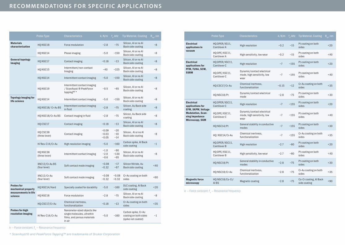
Materials characterization
HQ:NSC18 Force modulation ~2.8 ~75Silicon, Al or no Al Back side coating
~8
HQ:NSC14 Phase imaging ~5.0 ~150Silicon, Al or no Al Back side coating
~8
General topology imaging
HQ:NSC17 Contact imaging ~0.18 ~13Silicon, Al or no Al Back side coating
~8
HQ:NSC15Intermittent/non-contact Imaging
~40 ~325Silicon, Al or no Al Back side coating
~8
HQ:NSC14 Intermittent contact imaging ~5.0 ~150Silicon, Al or no Al Back side coating
~8
HQ:NSC19Intermittent contact imaging / ScanAsyst ® PeakForce tapping™ *
~0.5 ~65Silicon, Al or no Al Back side coating
~8
Topology imaging for life science
HQ:NSC14 Intermittent contact imaging ~5.0 ~150Silicon, Al or no Al Back side coating
~8
HQ:NSC18/ Cr-Au BSIntermittent contact imaging in fluid
~2.8 ~75Silicon, Au Back side coating
~8
HQ:NSC18/Cr-Au BS Contact imaging in fluid ~2.8 ~75Silicon, Au Back side coating
~8
HQ:CSC17 Contact imaging ~0.18 ~13Silicon, Al or no Al Back side coating
~8
HQ:CSC38 (three lever)
Contact imaging~0.09 ~0.03 ~0.05
~20 ~10 ~14
Silicon, Al or no Al Back side coating
~8
Hi’Res-C14/Cr-Au High resolution Imaging ~5.0 ~160Carbon spike, Al Back side coating
~1
HQ:NSC36 (three lever)
Intermittent contact imaging~1.0 ~2.0 ~0.6
~90 ~130 ~65
Silicon, Al or no Al Back side coating
~8
XNC12/Cr-Au BS (four lever) Soft contact mode imaging
~0.08 ~0.32
~17 ~67
Silicon Nitride, Au Back side coating
<40
XNC12/Cr-Au (four lever) Soft contact mode imaging
~0.08 ~0.32
~0.08 ~0.32
Cr-Au coating on both sides
<60
Probes for mechanical property measurements in life science
HQ:NSC14/Hard Specially coated for durability ~5.0 ~160DLC coating, Al Back side coating
< 20
HQ:NSC18 Force modulation ~2.8 ~75Silicon, Al or no Al Back side coating
~8
HQ:CSC17/Cr-AuChemical inertness, functionalization
~0.18 ~13Cr-Au coating on both sides
<35
Probes for high resolution imaging
Hi’Res-C14/Cr-Au
Nanometer-sized objects like single molecules, ultrathin films, and porous materials in air
~5.0 ~160Carbon spike, Cr-Au coating on both sides (spike not coated)
~1
Probe Type Characteristics k, N/m fo, kHz Tip Material, Coating Rtip, nm
k — Force constant; fo — Resonance frequency
* ScanAsyst® and PeakForce Tapping™ are trademarks of Bruker Corporation
R e Co m m e N d at i o N s f o R s P e C i f i C a P P l i C at i o N s
k — Force constant; fo — Resonance frequency
Electrical applicatons in vacuum
HQ:DPER/XS11, Cantilever A
High resolution ~0.2 ~15Pt coating on both sides
<20
HQ:DPE/XSC11, Cantilever A
High sensitivity, low wear ~0.2 ~15Pt coating on both sides
<40
Electrical applications for PFM, TUNA, SCM, SSRM
HQ:DPER/XSC11, Cantilever C
High resolution ~7 ~155Pt coating on both sides
< 20
HQ:DPE/XSC11, Cantilever C
Dynamic/contact electrical mode, high sensitivity, low wear
~7 ~155Pt coating on both sides
< 40
HQ:CSC17/Cr-AuChemical inertness, functionalization
~0.15 ~12Cr-Au coating on both sides
< 35
HQ:NSC18/PtDynamic/contact electrical mode
~2.8 ~75Pt coating on both sides
< 30
Electrical applications for EFM, SKPM, Voltage Modulation, Scan-ning Impedance Microscopy, SGM
HQ:DPER/XSC11, Cantilever C
High resolution ~7 ~155Pt coating on both sides
<20
HQ:DPE/XSC11, Cantilever C
Dynamic/contact electrical mode, high sensitivity, low wear
~7 ~155Pt coating on both sides
< 40
HQ:NSC14/PtGeneral stability in conductive modes
~7 ~155Pt coating on both sides
<30
HQ: NSC14/Cr-AuChemical inertness, functionalization
~7 ~155Cr-Au coating on both sides
< 35
HQ:DPER/XSC11, Cantilever B
High resolution ~2.7 ~80Pt coating on both sides
< 20
HQ:DPE/XSC11, Cantilever B
High sensitivity, low wear ~2.7 ~80Pt coating on both sides
< 40
HQ:NSC18/PtGeneral stability in conductive modes
~2.8 ~75Pt coating on both sides
< 30
HQ:NSC18/Cr-AuChemical inertness, functionalization
~2.8 ~75Cr-Au coating on both sides
<35
Magnetic force microscopy
HQ:NSC18/Co-Cr/Al BS
Magnetic coating ~2.8 ~75Co-Cr coating, Al Back side coating
<90
Probe Type Characteristics k, N/m fo, kHz Tip Material, Coating Rtip, nm
2424
www.mikromasch.com
www.spmtips.com
Contacts
Toll Free (US): +1 866 SPMTIPS (776-8477)Phone (EU): +49 (0) 6441 2003561Headquarters: +359 (0) 2 865-8629 E-mail: [email protected] [email protected]
MikroMasch® Headquarters
Innovative Solutions Bulgaria Ltd.
48, Joliot Curie Str.1113 Sofia, Bulgaria
phone: +359 2 865-8629fax: +359 2 [email protected]
MikroMasch® USA
NanoAndMore USA Corp.
21 Brennan Street, Suite 10Watsonville, CA 95076, USA
Toll Free (US): +1 866 SPMTIPS (776-8477)phone: +1 831-536-5970
fax: +1 [email protected]
MikroMasch® Europe
NanoAndMore GmbH
Spilburg Bld. A1,Steinbühlstrasse 7D-35578 Wetzlar,
Germanyphone: +49 (0) 6441 2003561
fax: +49 (0) 6441 2003562 [email protected]
MikroMasch® is a trademark of NanoWorld AG operated by ISB Ltd.
August 2017