Embed Size (px)
Citation preview

IC-EMC Simulation of Electromagnetic Compatibility of Integrated Circuits

SUMMARY
1. CONTEXT
2. TECHNOLOGY TRENDS
3. MOTIVATION
4. WHAT IS IC-EMC
5. SUPPORTED STANDARD
6. EXAMPLES
CONTENTS

• Until mid 90’s, IC designers had no
consideration about EMC problems in
their design..
• Starting 1996, automotive customers
started to select ICs on EMC criteria
• Starting 2005, mobile industry
required EMC in System in package
• Starting 2015, massive 3D integration
will require careful EMC design
• “Urgent Need to Integrate EMC and
Product Safety into Engineering
Curriculum of Technical Universities”
CONTEXT - WHY EMC OF IC ?

CONTEXT - FROM SYSTEM TO INTEGRATED CIRCUIT EMC
Components
Equipment Carbon airplane
Boards
Radar
• Emission
Personal Devices
Safety systems
interferences
• Susceptibility
Hardware fault Software failure Function Loss

Technology
Complexity
Packaging
2004
130nm
Embedded blocks
2007
90nm
250M
Core DSPs
10 Mb Mem
2010
45nm
500M
Dual core Dual DSP
RF Graphic Process.
100 Mb Mem Sensors
2013
28nm
2G
Quad Core Quad DSP
3D Image Proc Crypto processor
Reconf FPGA, Multi RF
1 Gb Memories Multi-sensors
7G
Mobile generation 3G 3G+ 4G
5nm
150 G
2020
?
5G
TECHNOLOGY TRENDS TOWARDS TERA DEVICES
14nm
2016
4G+
Today
Octa Core Multi DSP
3D 4K Image Proc Crypto, sensor,
position processor Agregated RF
2 Gb Memories
15G
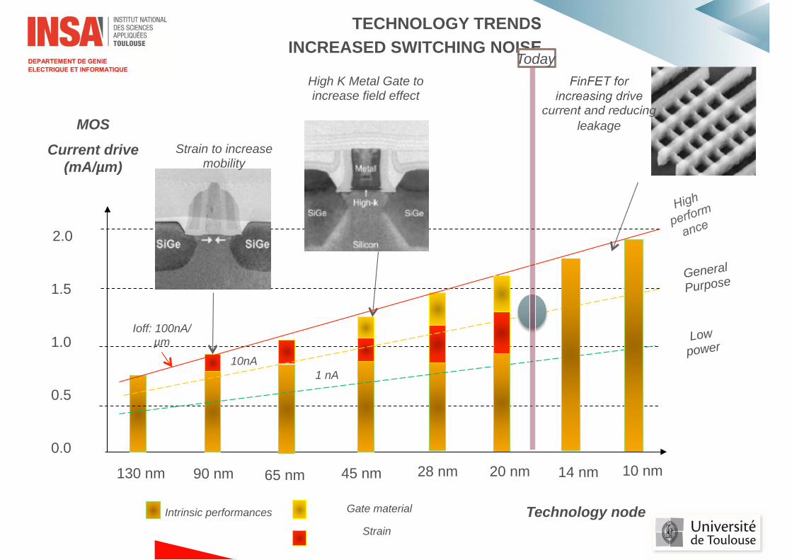
MOS
Current drive (mA/µm)
2.0
1.0
0.0
130 nm
1.5
0.5
45 nm 65 nm 20 nm 28 nm
Technology node Intrinsic performances
Strain
Gate material
90 nm
Strain to increase mobility
High K Metal Gate to increase field effect
Ioff: 100nA/µm
10nA 1 nA
TECHNOLOGY TRENDS INCREASED SWITCHING NOISE
14 nm
FinFET for increasing drive
current and reducing leakage
10 nm
Low power
General
Purpose
Today

5.0
3.3
2.5
1.8
0.35µ 0.18µ 90n 65n
Technology node
1.0
Supply (V)
1.2
45n
I/O supply
Core supply
32n 20n 14n 130n 10n 7n
0.8 V inside, 1.2V
outside
14-nm technology
TECHNOLOGY TRENDS DECREASED NOISE MARGIN
• VDD is lowered to 800mV in 14-nm technology
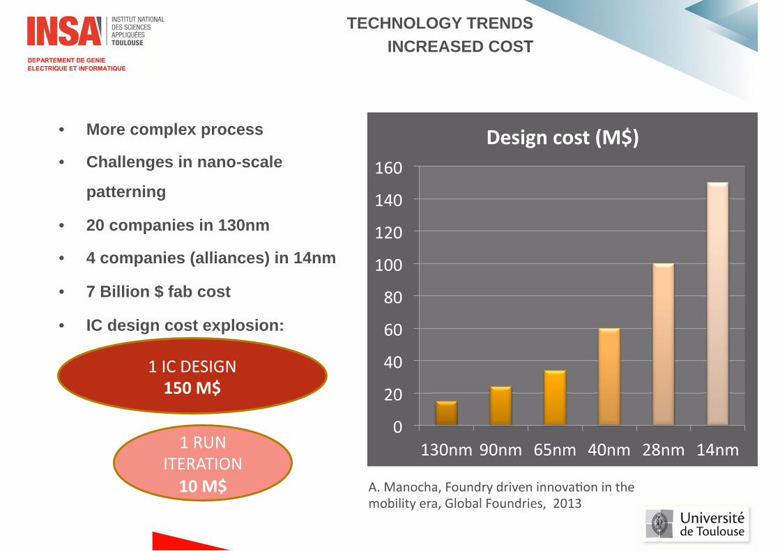
• More complex process
• Challenges in nano-scale
patterning
• 20 companies in 130nm
• 4 companies (alliances) in 14nm
• 7 Billion $ fab cost
• IC design cost explosion:
TECHNOLOGY TRENDS INCREASED COST

DESIGN
Architectural Design
Design Entry Design Architect
FABRICATION
EMC compliant
EMC Simulations Compliance ?
GO
NO GO
Design Guidelines
Tools
Training
• Lack of tools, guidelines and training in EMC of
Integrated circuits, for improved EMC before fabrication
MOTIVATION

• A schematic editor • An interface to Spice analog simulation • A post-processor to compare simulated
with measured spectrum • An Electromagnetic solver for radiated field • Freeware, online • 250 pp documentation, 15 case studies • 1-week trainings
WHAT IS IC-EMC
Spectrum analysis
Impedance simulation
Near-field simulation
Immunity simulation
IBIS interface
Key tools
Smith Chart
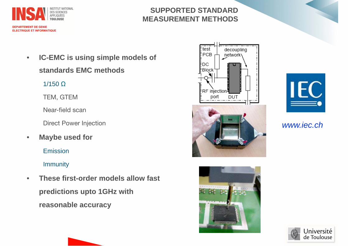
• IC-EMC is using simple models of
standards EMC methods
1/150 Ω
TEM, GTEM
Near-field scan
Direct Power Injection
• Maybe used for
Emission
Immunity
• These first-order models allow fast
predictions upto 1GHz with
reasonable accuracy
SUPPORTED STANDARD MEASUREMENT METHODS
www.iec.ch

• IC-EMC illustrates concrete application of IBIS, ICEM and ICIM models for EMC
prediction
STANDARDS
SUPPORTED STANDARD MODELLING METHODS
1. ICEM-CE - Conducted RF emission 2. ICEM-RE - Radiated RF emission
4. ICIM-CI - Conducted RF immunity
4. ICIM-RI - Radiated RF immunity
www.iec.ch

• Z(f) measurements
based on [s] using
network analyzer and
microwave probes
• Package pitch: 1mm
down to 250µm
• Frequency of interest:
1 MHz – 10 GHz
EXAMPLE 1 – IMPEDANCE MODELLING

Measurement
Model
C=4.5 pF
R=25
Connectors PCB Package
IC
Z(f)
• Tune R,L,C based model
from measured Z(f)
• Identify dominant
parameters and to link the
values to physical
characteristics
• Package impedance
• On-chip impedance
• PCB tracks impedance
• Discrete R,L,C
• EMC probes
EXAMPLE 1 – IMPEDANCE MODELLING

Core Model
Package Model
Probe Model
Test board Model
Analog Time Domain Simulation
Fourier Transform
Compare dBµV vs. Frequency
Frequency measurements
Simulation Measurements
IEC 62 433
IEC 61 967
• Build emission model
• Tune a model from
measured spectrum
(1/150 Ω method)
• Identify dominant
parameters (I, L,C..) and
to link the values to IC
characteristics
• Number of gates
• On-chip decoupling
• Supply pairs
EXAMPLE 2 – PREDICT CONDUCTED EMISSION

• Freescale MPC 5534 case study
• One core, two BGA package
versions (208, 324 pins)
EXAMPLE 2 – PREDICT CONDUCTED EMISSION

EXAMPLE 2 – PREDICT CONDUCTED EMISSION
30
20
10
0
-102M 3M 5M 10M 20M 30M 50M 100M 200M 300M 500M 1G
Conducted emission measurement on 3.3V supply
Conducted emission simulation on 3.3V supply
Amplitude (dBµV)
30
20
10
0
-102M 3M 5M 10M 20M 30M 50M 100M 200M 300M 500M 1G
Conducted emission measurement on 3.3V supply
Conducted emission simulation on 3.3V supply
Amplitude (dBµV)
30
20
10
0
-102M 3M 5M 10M 20M 30M 50M 100M 200M 300M 500M 1G
Conducted emission measurement on 3.3V supply
Conducted emission simulation on 3.3V supply
Amplitude (dBµV)
30
20
10
0
-102M 3M 5M 10M 20M 30M 50M 100M 200M 300M 500M 1G
Conducted emission measurement on 3.3V supply
Conducted emission simulation on 3.3V supply
Amplitude (dBµV)

• Immunity modelling does not
concern only the IC
• The power injection setup
must be modeled with care
Power amplifier
Coupler
Forward, reflected Power
PCB Injection path
Coupling to IC
• The Input/output structures of
the IC are critical
• The IC failure criteria is an
opened issue
EXAMPLE 3 – PREDICT IMMUNITY
Device under test
Power injection

• A model can be
tuned from measured
immunity
measurement (DPI
method)
• Exploit coupler,
power extraction,
susceptibility criteria.
• IC-EMC eases the
iterative simulation
EXAMPLE 3 – PREDICT CONDUCTED IMMUNITY
Aggressed IC Model (ICEM)
Package and IO model (IBIS)
RFI and coupling path model (Z(f))
Set RFI frequency IC-EMC
Increase V aggressor
Time domain simulation
WinSPICE
Criterion analysis
Extract forward power
IC-EMC
Increase frequency

• 16 bit micro-controller�
• Direct power injection�
• Input buffer aggression�
• Sinusoidal mode�
• Simulation criterion: Logical
change of input buffer�
EXAMPLE 3 – PREDICT CONDUCTED IMMUNITY

• Radiating elements representing local magnetic
field sources, associated to inductances
• Extreme simplification of thousands of
elementary sources
EXAMPLE 4 RADIATED EMISSION

• Power
domain
floorplan
analysis
enables to
visalize
unbalanced
networks
• Risk of
loops and
radiation
EXAMPLE 4 RADIATED EMISSION

• NFS measurement vs simulation of Hz of a
System-on-chip with DDR supply network
EXAMPLE 4 RADIATED EMISSION
(a) measurement (b) simulation
-35dBA/m
-35dBA/m
-55dBA/m
-55dBA/m

Lower BGA to board (0.4mm pitch)
Upper BGA to memories (0.5mm pitch)
2 channels of 32-bit 1.2V
DDR3, 5 GB/s
EXAMPLE 5 3D PACKAGE ON PACKAGE
• Merge of two IBIS of different ICs. SI/PI prospective analysis

• An environment for EMC
prediction at IC level and
trainings has been developed
• The IC-EMC tool is a freeware
• Several IC case study
available (measurements,
models)
• Continuing education in EMC
of ICs based on
measurements & simulations
• Close contact with industry
for case-study analysis
CONCLUSION
www.emccompo.org, Nov. 2015

Merci pour votre attention