Embed Size (px)
Citation preview

MICROWAVE METAMATERIAL APPLICATIONS USING
COMPLEMENTARY SPLIT RING RESONATORS AND HIGH
GAIN RECTIFYING REFLECTARRAY FOR WIRELESS POWER
TRANSMISSION
A Dissertation
by
CHI HYUNG AHN
Submitted to the Office of Graduate Studies of
Texas A&M University
in partial fulfillment of the requirements for the degree of
DOCTOR OF PHILOSOPHY
August 2010
Major Subject: Electrical Engineering

MICROWAVE METAMATERIAL APPLICATIONS USING
COMPLEMENTARY SPLIT RING RESONATORS AND HIGH
GAIN RECTIFYING REFLECTARRAY FOR WIRELESS POWER
TRANSMISSION
A Dissertation
by
CHI HYUNG AHN
Submitted to the Office of Graduate Studies of
Texas A&M University
in partial fulfillment of the requirements for the degree of
DOCTOR OF PHILOSOPHY
Approved by:
Chair of Committee, Kai Chang
Committee Members, Robert D. Nevels
Laszlo Kish
Hae-Kwon Jeong
Head of Department, Costas N. Georghiades
August 2010
Major Subject: Electrical Engineering

iii
ABSTRACT
Microwave Metamaterial Applications Using Complementary Split Ring
Resonators and High Gain Rectifying Reflectarray for Wireless Power
Transmission. (August 2010)
Chi Hyung Ahn, B.S., Inha University;
M.S., Pohang University of Science and Technology
Chair of Advisory Committee: Dr. Kai Chang
In the past decade, artificial materials have attracted considerable attention
as potential solutions to meet the demands of modern microwave technology for
simultaneously achieving component minimization and higher performance in
mobile communications, medical, and optoelectronics applications. To realize this
potential, more research on metamaterials is needed.
In this dissertation, new bandpass filter and diplexer as microwave
metamaterial applications have been developed. Unlike the conventional
complementary split ring (CSRR) filters, coupled lines are used to provide larger
coupling capacitance, resulting in better bandpass characteristics with two CSRRs
only. The modified bandpass filters are used to deisgn a compact diplexer. A new
CSRR antenna fed by coplanar waveguide has also been developed as another
metamaterial application. The rectangular shape CSRRs antenna achieves dual
band frequency properties without any special matching network. The higher

iv
resonant frequency is dominantly determined by the outer slot ring, while the lower
resonant frequency is generated by the coupling between two CSRRs. The
proposed antenna achieves about 35% size reduction, compared with the
conventional slot antennas at the low resonant frequencies.
As a future alternative energy solution, space solar power transmission and
wireless power transmission have received much attention. The design of efficient
rectifying antennas called rectennas is very critical in the wireless power
transmission system. The conventional method to obtain long distance range and
high output power is to use a large antenna array in rectenna design. However, the
use of array antennas has several problems: the relatively high loss of the array
feed networks, difficultiy in feeding network design, and antenna radiator coupling
that degrades rectenna array performance.
In this dissertation, to overcome the above problems, a reflectarray is used to
build a rectenna system. The spatial feeding method of the reflectarray eliminates
the energy loss and design complexity of a feeding network. A high gain rectifying
antenna has been developed and located at the focal point of the reflectarray to
receive the reflected RF singals and genterate DC power. The technologies are very
useful for high power wireless power transmission applications.

v
DEDICATION
To my mother and the memory of my father,
my two sisters, and my lovely wife and son

vi
ACKNOWLEDGMENTS
I would like to express my deepest appreciation to Dr. Kai Chang for his
support and guidance throughout my Ph.D. education at Texas A&M University. I
also appreciate Dr. Robert D. Nevels, Dr. Laszlo Kish, and Dr. Hae-Kwon Jeong
for serving as my committee members and for their helpful comments.
I would also like to thank Mr. Ming-Yi Li for his technical assistance. I
gratefully acknowledge Mr. Seongwon Oh, Mr. Jeongkyu Lee, Mr. Chanho Kim,
Mr. Travis Eubanks, Mr. Jihyung Yu, Mr. Jonathan Hansen, Mr. Dongjin Jeong,
and other members of the Electromagnetics and Microwaves Laboratory at Texas
A&M University for invaluable discussions. I would also like to give special
thanks to Yu-Juin Ren at RIM Inc., Dr. Chulmin Han at Ethetronics Inc. and Dr.
Shih-Hsun Hsu at AOI Inc. for their helpful suggestions in the development of the
technologies described in this dissertation.
Lastly, I would like to express my deep appreciation to my mother and my
two sisters for their constant love, encouragement, and support. I also thank my son,
Woojin for his love. Finally, my sincere thanks are given to my lovely wife,
Soyoung, for all her patience, love, and support during my graduate studies.

vii
TABLE OF CONTENTS
Page
ABSTRACT ..................................................................................................................... iii
DEDICATION ................................................................................................................... v
ACKNOWLEDGMENTS ................................................................................................. vi
TABLE OF CONTENTS .................................................................................................vii
LIST OF FIGURES ........................................................................................................... ix
LIST OF TABLES ......................................................................................................... xiii
CHAPTER
I INTRODUCTION ................................................................................................... 1
1. Background ........................................................................................................ 1
2. Dissertation Organization .................................................................................. 4
II FUNDAMENTALS OF METAMATERIALS ....................................................... 7
1. Introduction ........................................................................................................ 7
2. Fundamentals of Metamaterials ......................................................................... 7
3. Metamaterial Resonators –SRR/CSRR ............................................................ 12
4. Summary .......................................................................................................... 17
III COMPACT PARALLEL COUPLED LINE BAND-PASS FILTER AND
DIPLEXER USING COMPLEMENTARY SPLIT RING RESONATORS ......... 18
1. Introduction ...................................................................................................... 18
2. Single CSRR Resonator and Its Equivalent Circuit ......................................... 19
3. Compact Band-Pass Filter Design.................................................................... 24
4. Diplexer Design Based on CSRRs ................................................................... 29
5. Summary .......................................................................................................... 35
IV DUAL BAND COMPLEMENTARY SPLIT RING ANTENNA FED BY
COPLANAR WAVEGUIDE.................................................................................. 36

viii
CHAPTER Page
1. Introduction ...................................................................................................... 36
2. CSRR Antenna Design .................................................................................... 37
3. Measured Results ............................................................................................. 38
4. Summary .......................................................................................................... 43
V HIGH GAIN RECTIFYING ANTENNA .............................................................. 47
1. Introduction ...................................................................................................... 47
2. Wireless Power Transmission System ............................................................. 48
3. Rectenna Operation Theory ............................................................................. 51
4. High Gain Rectenna Element Design ............................................................... 62
5. Summary .......................................................................................................... 67
VI RECTIFYING ANTENNA ARRAY USING REFLECTARRAY ....................... 69
1. Introduction ...................................................................................................... 69
2. Reflectarray Operation Theory ......................................................................... 70
3. Reflectarray Component Design ...................................................................... 78
4. Rectifying Reflectarray .................................................................................... 82
5. Summary .......................................................................................................... 85
VII MICROWAVE APPLICATIONS: WIDEBAND COPLANAR STRIPLINE
TO DOUBLE-SIDED PARALLEL-STRIP LINE TRANSITION AND
DUAL BAND OMNI-DIRECTIONAL ANTENNA FOR POLARIZATION
DIVERSITY ........................................................................................................... 88
1. Introduction ..................................................................................................... 88
2. Double-Sided Parallel-Strip Line .................................................................... 91
3. Wideband CPS to DSPSL Transition ............................................................... 93
4. Dual Frequency Omni-directional Antenna ..................................................... 98
5. Summary ........................................................................................................ 108
VIII SUMMARY AND RECOMMENDATIONS ...................................................... 109
1. Summary ........................................................................................................ 109
2. Recommendations for Future Research ......................................................... 112
REFERENCES ............................................................................................................... 113
VITA .............................................................................................................................. 125

ix
LIST OF FIGURES
FIGURE Page
Fig. 1. Classifcation of materials (DPS : double positive, ENG: epsilon negative,
DNG: double negative, MNG: mu negative) ....................................................... 11
Fig. 2. Structures of (a) the first SRR tube and (b) early SRR element ........................... 12
Fig. 3. (a) Pendry‟s SRR and (b) its simplified equivalent circuit ................................... 13
Fig. 4. (a) The sophisticated equivalent model of the SRR, (b) its unit cell model,
and (c) solved equivalent circuit of the SRR ........................................................ 14
Fig. 5. (a) CSRR structure and (b) its equivalent model .................................................. 16
Fig. 6. (a) Unit cell of conventional CSRR BPFs with series coupling feed lines
and (b) the proposed single CSRR structure with parallel coupling feed
lines (Black and white part represents microstrip lines on top and etched
CSRR on ground plane, respectively.) ................................................................. 20
Fig. 7. Equivalent circuit model of the structures in Fig. 6 .............................................. 21
Fig. 8. Simulated results of different (a) series gap distances and (b) microstrip line
stub lengths ........................................................................................................... 23
Fig. 9. The proposed double CSRR bandpass filter ( L1 = 5.4 mm, L1 = 8 mm, g1 =
0.2 mm, g2 = 0.36 mm, g3 = 0.5 mm, g4 = 0.2 mm, Wf = 1.6 mm ) ...................... 25
Fig. 10. Simulation results of (a) open stub length effect and (b) parallel coupled
gap distance effect ................................................................................................ 26
Fig. 11. Measured and simulated results of a prototype double CSRRs BPF .................. 27
Fig. 12. Pictures of double CSRRs BPF: (a) front view and (b) backside view .............. 28
Fig. 13. Diplexer schematic .............................................................................................. 29
Fig. 14. (a) Structure of a CSRR BPF with four ports and (b) its simulated results ........ 30
Fig. 15. Simulated results of two separated filters ........................................................... 31
Fig. 16. Structure of the proposed diplexer ( Lst1 = 0.49 mm, g1 = 0.36 mm, g2 =
0.18 mm, g3 = 0.46 mm, g4 = 0.46 mm, Lst2 = 0.98 mm, dpg1 = 7.5mm, dpg2
= 9.1 mm) ............................................................................................................. 32

x
FIGURE Page
Fig. 17. (a) Simulated and (b) measured results of the proposed diplxer ........................ 33
Fig. 18. Pictures of the proposed diplexer: (a) front view and (b) backside view ........... 34
Fig. 19. Configuration of the proposed dual-frequency CSRR antenna .......................... 38
Fig. 20. Measured results of the different CSRR sizes .................................................... 40
Fig. 21. Measured results of different CSRR widths ....................................................... 41
Fig. 22. (a) Measured and (b) simulated results of different distances of dr .................... 42
Fig. 23. Measured and simulated radiation patterns of antenna A in (a) elevation
and (b) azimuth plane ( : simulated result at 2.6 GHz, : measured
result at 2.6 GHz, : simulated result at 2.6 GHz, and : measured
result at 4.4 GHz) ................................................................................................. 44
Fig. 24. Measured gains of the proposed antenna at (a) 2.6 GHz and (b) 4.5 GHz ......... 45
Fig. 25. The fabricated CSRR antenna ............................................................................. 46
Fig. 26. Wireless power transmission system schematic. ................................................ 49
Fig. 27. Rectenna block diagram. ..................................................................................... 50
Fig. 28. (a) Half-wave rectifier with capacitor and (b) its waveforms ............................ 52
Fig. 29. Diode current-voltage characteristic curves with the incident fundamental
and diode junction voltage waveforms. ................................................................ 54
Fig. 30. Equivalent circuit model of the half-wave rectifier. ........................................... 56
Fig. 31. Configuration of the proposed high gain rectenna with pentagonal loops. ........ 63
Fig. 32. Simulated input impedance of the antenna. ........................................................ 64
Fig. 33. Simulated antenna gain. ...................................................................................... 64
Fig. 34. Free space measurement setup of the rectenna ................................................... 67
Fig. 35. Measured rectenna efficiency at 5.8 GHz ........................................................... 68
Fig. 36. Geometry of a microstrip reflectarray ................................................................. 71

xi
FIGURE Page
Fig. 37. Reflectarray block diagram ................................................................................. 71
Fig. 38. Directivity vs. q factor of the feed ...................................................................... 75
Fig. 39. The real antenna pattern vs. cosq pattern
( : real antenna pattern, : cosq pattern) ................................................ 75
Fig. 40. Reflectarray configuratio for spillover efficiency ............................................... 76
Fig. 41. Aperture efficiency vs. F/D ................................................................................. 79
Fig. 42. Efficiency vs. F/D ............................................................................................... 79
Fig. 43. 3D configuration of the reflectarray ................................................................... 80
Fig. 44. Unit reflectarray element and its picture ............................................................. 81
Fig. 45. Phase variation of the unit cell element .............................................................. 81
Fig. 46. Feed antenna: (a) top view and (b) side view ..................................................... 83
Fig. 47. Measured radiation patterns of the feed antenna in elevation plane ................... 83
Fig. 48. Reflectarray with the feed antenna ..................................................................... 84
Fig. 49. Measured radiation pattern of the reflectarray at 5.8 GHz ................................. 84
Fig. 50. Rectifying antenna: (a) top view and (b) side view ............................................ 86
Fig. 51. Measured conversion efficiency of the rectifying reflectarray ........................... 86
Fig. 52. Configurations of (a) symmetrical double-sided parallel-strip line and (b)
conventional microstrip line. ................................................................................ 92
Fig. 53. Configurations of the proposed CPS to DSPSL transition: (a) 3D view, (b)
top side, and (c) bottom side................................................................................. 95
Fig. 54. Cross-sectional views of the proposed transition and electric field
distributions: (a) CPS mode, (b) Transition mode, and (c) DSPSL mode .......... 96
Fig. 55. Simulated and measured results of a CPS to DSPSL back to back transition .... 97

xii
FIGURE Page
Fig. 56. (a) Top plane conductor and its current distributions, (b) bottom plane
conductor and its current distributions, (c) top view of the combined
antenna and current distributions, and (d) side view of the proposed antenna ..... 99
Fig. 57. Simulation and measurement results of return loss .......................................... 100
Fig. 58. Simulation results of wing length‟s effect ........................................................ 100
Fig. 59. Simulation results of wing width‟s effect ......................................................... 102
Fig. 60. (a) Simulated result of return loss of stub length, (b) radiation pattern in
azimuth plane at 3.9 GHz with t1 = 0.0 mm and t2 = 0.0 mm, and (c)
radiation pattern in azimuth plane at 3.9 GHz with t1 = 0.4 mm and t2 = 0.0
mm ...................................................................................................................... 103
Fig. 61. Simulated and measured radiation patterns at 2.45 GHz: (a) x-y plane and
(b) y-z plane ........................................................................................................ 105
Fig. 62. Simulated and measured radiation patterns at 3.9 GHz: (a) x-y plane and
(b) y-z plane ........................................................................................................ 106
Fig. 63. The fabricated antenna (left: top view, right: bottom view) ............................. 107

xiii
LIST OF TABLES
TABLE Page
1. Extracted lumped elements. .................................................................................... 22
2. Measured results of the four prototype antennas .................................................... 40
3. The design parameters of the dual band omnidirectional loop antenna
[unit:mm] ................................................................................................................ 98

1
CHAPTER I*
1. INTRODUCTION
1. Background
A. Left-Handed Metamaterials
This dissertation is divided into two main topics. Topic one covers metamaterial
applications applied to novel microwave antenna and filter designs using complementary
split ring resonators. Topic two covers a microwave rectifying reflectarray for wireless
power transmission.
The history of metamaterials started in 1967 with a theoretical investigation by
Russian physicist Viktor Veselago. One year later, the paper was published in English as
“ The electrodynamics of substances with simultaneously negative values of ε and μ ”
[1]. Veselago‟s hypothesis on the substances with negative dielectric constant and the
negative magnetive permeability, which was called left-handed substances in the paper,
leads to very unusual electromagnetic phenomenons; left-handed wave propagation and
a negative refractive index as compared with ordinary materials. These unique
electromagnetic characteristics were not investigated further because no realization of
any artificial components with these properties hypothsized existed at that time. In 1998
______________
This dissertation follows the style of IEEE Transactions on Microwave Theory and Techniques.

2
and 1999, J. B Pendry published two important papers about a thin wire component
producing negative permittivity and positive permeability [2] and a split ring resonator
(SRR) producing negative permeability and positive permittivity [3]. In 2000, he
introduced the concept of superlenses, negative refractive index materials, which are
able to reproduce perfect 2D images of both the propagating waves and evanescent
waves of an object [4]. Pendry‟s contributions inspired the first left-handed structure
realization. In 2000, D. R. Smith et al. [5] experimentally succeeded in synthesizing the
first left-handed substance producing negative effective permittivity and permeability,
33 years after Veselago‟s hypothesis. This composite structure was combined of
Pendry‟s two structures: a thin wire structure and a split ring resonator. This paper
showed electromagnetic wave propagation experimentally at certain resonant band when
effective ε and μ are both negative, and compared with the non propagation
characteristics when one of the constants is negative. Finally, Smith and Shelby
experimentally verificate a negative refracive index in 2001 [6].
In recent years, metamaterials have been greatly attentioned for many possible
uses in microwave and optics fields. Many metamateiral applications about the
backward coupler, phase compensation resulting in electrically small resonators, sub-
wavelength waveguides with lateral dimensions below diffraction limits, and Čerenkov
radiation, and doppler effect have been studied [7]-[14].
B.Wireless Power Transmission
The history of wireless power transmission started with a successful experiment by

3
Nikola Tesla [15] over a hundred year ago. He made it to transmit wireless power from
his oscillators operating up to 100 MV at 150 KHz to two bulbs. From this success,
several WPT studies had been conducted in Japan [16] and U.S. [17] in the 1920‟s and
1930‟s. In the 1950‟s, the development of high power and efficiency micrwave tube by
Raytheon Company [18] opened the modern WPT era.
The first rectenna was invented in the 1960‟s by combining a half-wave dipole
antenna and a single diode by W.C. Brown for 2.45GHz RF-to DC power conversion
[19]. To achieve high conversion efficency, Brown later used a GaAs-Pt shottky barrier
diode and aluminum bar dipole with 90.6 % conversion efficiency in 1977 [20].
The 1970‟s oil embargo encouraged the proposal for a solar power satellite (SPS)
by P. E. Glaser [21] leaded great development on microwave power transmission
technology. The SPS collects solar energy directily from space and transfers it to ground
stations on the earth using microwave power transmission technology [22]-[23]. The
possibiltiy of SPS as a future energy solution resulted in the great improvement of the
rectenna technology.
The technology of a large-scale wireless power transmission are necessary for
efficient SPS system, and normally many rectennas are combined into an array to rectify
large amount of power. In 1975, the Jet Propulsion Laboratory and Raytheon built a 18 x
24 ft2 rectenna array with 5000 elements working at 2.45 GHz [24]. A 30 kW output
power of the rectenna array was achieved at a distance of one mile. In 1998, N.
Shinohara in Japan built another 2.45 GHz rectenna array consisting of 2,294 dipoles for
high power conversion [25]. In 2000, a dual-polarized rectenna array at 8.51 GHz was

4
developed by JPL with 50 V output [26]. In 2003, B. Strassner and K. Chang at Texas
A&M University reported a C-band circularly polarized high efficency rectenna array
with high gain rhombic loop antennas [27]-[28].
Several rectenna array types have been studied with high gain properties to
achieve long distance WPT, higher DC power output, and reduced receiving areas. The
rectenna array design has several challenges including design difficulties and the
relatively high loss of array feeding networks, and antenna element coupling causing
reduced rectenna array performance. A new rectenna array design method was necessary
to overcome these challenges.
The rectenna array design presented in this dissertation combines a high gain
single rectenna element with a reflectarray instead of array antenna elements. The
reflectarray has several advantages over the parabolic reflector antenna (the most often
used high gain antenna), such as: being flat, having a low-profile, and being easier to
manufacture [29]-[30]. The reflectarray features can be adapted to a rectenna for the
WPT system. The reflectarray normally achieves high gain and a feed network is not
needed. A linearly polarized pentagonal loop rectenna with high gain can be used and
placed at the reflectarray focal point to rectify the received microwave energy. The
proposed novel rectenna array suggests a new type of long distance MPT system.
2. Dissertation Organization
This dissertation covers a variety of topics, consisting of microwave parallel
coupled line bandpass filter and diplexer based on CSRRs, dual frequency CSRR

5
antenna fed by CPW, high gain rectifying reflectarray, wideband transition between
coplanar stripline to double-sided parallel-strip line, dual band omni-directional antenna,
and dual polarized conformal array antenna. Eight chapters comprise this dissertation.
Chapter II reviews the fundalmental theory of left-handed metamaterials with
electromagnetic theories. Theoretical analysis for negative phase constant, negative
phase velocity, and negative index of refraction in DNG medium are described. Then
realization of metamaterial components, especially for SRR and CSRR, are presented.
Chapter III introduces a new design for microwave compact bandpass filter and
diplexer based on complementary split ring resonators. The parallel coupled
transmission lines on one CSRR is analyzed with its equivalent circuit model. Then a
compact bandpass filter design using dual CSRRs is discussed. This bandpass filter does
not need multi-casecades for improved bandpass characteristics. Finally, based on the
CSRR bandpass filter design concept, a compact microwave diplexer casecading two
parallel coupled line CSRR filters is proposed.
Chapter IV presents a novel complementary split ring resonator antenna fed by
complanar waveguide. Two concentric slot rings with split generate dual resonating
frequencies at 2.6 GHz and 4.5 GHz. The CPW fed slot antenna does not need any
special matching networks for good impedance matching. For better understanding of
the proposed antenna‟s characteristics, several design parameters are analyzed.
Chapter V reviews WPT system and rectenna operation theory. A high gain
rectenna based on CPS structrue is presented. A dual pentagonal loop antenna generates
a high gain of 10.2 dBi. The proposed antenna is used for a cominbed rectifying

6
reflectarray as a feed antenna. Maximum conversion efficiency of the single element is
75%.
Chapter VI discusses a new rectifying array antenna combining a reflectarry with
23 x 24 elements of a high gain 5.8 GHz rectenna element. The reflectarray with
compact unit cells, a combination of inner circlular patch and outer ring, is discussed. A
rectenna element located at the focal point of the reflectarray consists of 2X1 pentagonal
loop antennas. The proposed rectenna element shows 10.2 dBi high gain at 5.8 GHz. The
performances of combination of a reflectarray and a rectenna element is presented. The
conversion efficiency of the rectifying reflectarray goes up to 71 %.
Chapter VII introduces two microwave applications. By using the basic theory of
double-sided parallel-strip line (DSPSL), wideband CPS to DSPSL transition is
developed. The transition achieves low insertion loss from 2.4 GHz to 10.7 GHz. A dual
frequency omni-directional antenna is discussed. The antenna provides horizontally
polarized radiation patterns, which is useful for polarization diversity application for
MIMO systems.
Chapter VIII concludes this dissertation with a summary, discussion of the
research accomplishments, and recommendations for future studies.

7
CHAPTER II
FUNDAMENTALS OF METAMATERIALS
1. Introduction
Metamaterials are defined as artificial effectively homogenous electromagnetic
structures with unusual properties not readily available in nature. More than 40 years
have passed since Veselago‟s first theoretical investigation [1] of left-handed material
simulatenously exhibiting negative permittivity and permeability. In the last decade, the
artificial materials have attracted considerable attention as potentional solutions to meet
the demands of modern microwave technology for simultaneously achieving component
minimization and higher performances in mobile communications, medical, and
optoelectronics applications [31]-[35].
2. Fundamentals of Metamaterials
To understand the fundamentals of left-handed metamaterials exhibiting
antiparallelism between the phase and group velocities, and negative refractive index in
left-handed materials, Maxwell‟s equations are reiterated in the frequency domain.
E j B M (1)
H j D J (2)
eD (3)

8
MB (4)
where E [V/m] and H [H/m] are the electric and magnetic field intensity, respectively,
and D [C/m2] and B [W/m
2] are the electric and magnetic flux density, respectively, J
[A/m2] and M [V/m
2] are the electric and magnetic current density, respectively, and
e [C/m3] and m [C/m
3] are the electric and magnetic charge density, respectively. In
linear and nondispersive medium, the constituitive equations are given by
' "
0 0( )r r rD E j E (5)
' "
0 0( )r r rB H j H (6)
where 12
0 8.854 10 [F/m] is the permittivity and 7
0 4 10 [H/m] is the
permeability of free space, and '
r and '
r are the medium‟s relative permittivity and
permeability, respectively, and "
r and "
r are the losses in r and r , respectively, due
to dielectric and magnetic damping and finite conductivity. Note that "
r and "
r must be
positive due to the conservation of energy.
For simplicity, the medium is lossless (" 0r ,
" 0r ) in source free ( 0M ,
0J ) region. From Maxwell‟s equations, Helmholtz‟s equations to obtain E and H
can be expressed as
22 0E k E (7)
22 0H k H (8)
where 2 2k is the propagation constant. The propagation constant can be defined

9
for the medium as k j where is the attenuation constant and is the phase
constant. In the lossless case, = 0 and k j . Phase constant is expressed by
(9)
With the equations above, observation shows how medium characteristics ( ,r r )
affect electromagnetic fields ( , ) traveling through the medium in four different
cases.
A. Double Positive (DPS) Medium ( 0r , 0r )
When 0r and 0r , phase constant in equation (9) is
(10)
By substituting the expressinos of the plane wave in these mediums into the first two
Maxwell‟s equations, the following relations among the wave vector, the electric
intensities, and magnetic intenisities are obtained.
E H (11)
H E (12)
These results show that the electric field intensity E , the magnetic field intensity H ,
and the wave vector build a right-handed triad.
B. Double Negative (DNG) Medium ( 0r , 0r )
When 0r and 0r , phase constant and field relations are
' ' . (13)

10
E H (14)
H E (15)
These results indicate that in DNG medium, the electric field intensity E , the magnetic
field intensity H , and the wave vector build a left-handed triad.
C. Epsilon Negative (ENG) ( 0r , 0r ) & Mu Negative (MNG) ( 0r , 0r )
Medium
In the ENG case ( 0r and 0r ) or MNG ( 0r , 0r ), both phase
constants are
0 (16)
which means that the waves in this medium become evanescent waves and do not
propagate ( 0 ). The phase velocity in a medium is defined as
pv
(17)
The case studies show that the phase constant in a left-handed medium (DNG) is
negative since the phase constant is positive in DPS medium, and phase velocity pv in
DNG becomes negative and pv becomes positive in DPS medium. All lossless materials
in terms of the signs of permittivity r and permeability r can be classified as shown
in Figure 1.
Another interesting characteristic with negative phase constant can be found with
the following equation.

11
0nk nc
(18)
where refractive index n is
r rn (19)
These equations indicate that the refractive index becomes negative in a DNG medium
(negative permittivity and negative permeability) due to negative phase constant while it
is positive in a DPS medium.
plasma
wire structure
split rings structure
ferrites
No transmission
No transmission
air air
air air
(Permittivity)
ENG ( 0, 0 ) DPS ( 0, 0 )
DNG ( 0, 0 )
MNG ( 0, 0 )
n
n
(Permeability)
Conventional
materials
Left-handed
materials
Fig. 1. Classifcation of materials (DPS : double positive, ENG: epsilon negative, DNG:
double negative, MNG: mu negative)

12
3. Metamaterial Resonators – SRR/CSRR
The first „split ring resonator‟ was invented by Hardy [36] in 1981 as shown in
Figure 2(a). The structure consists of two metallic tubes with a split on inner tube only.
The gap between two tubes increases capacitance and the outer tube impounds the
magnetic field to make outer region magnetic flux equal to the inner region magnetic
flux as
O iBS BS (20)
Where Si = π Ri2, So = π [Ro
2 – (Ri + w)
2] and w is the inner tube thickness and Ro and Ri
are the radii of the outer and inner structures, respectively. The resonant frequency of the
split ring tube resonator can be determined as
1 iO
o i
S g cW w
S R (21)
where g is the split width. This structure, based on the analytical equation, was available
gRo
Ri
w
(a) (b)
Fig. 2. Structures of (a) the first SRR tube and (b) early SRR element

13
from 20 MHz to 2 GHz. A frequency range extension to 4 GHz was researched by Zonta
[37]. In 1993, another metallic element to achieve artificial medium effect was
introduced [38] shown in Figure 2 (b). Metallic structure resonance was achieved by
combining capacitance and inductance configurations.
Pendry in 1999 [3] introduced a conducting non-magnetic ring array, which
became popular metamaterial components called SRRs. The difference from other early
elements in configuration is that Pendry‟s structure consists of two concentric rings with
splits on opposite sides as shown in Figure 3 (a). Inductance from the structure can be
obtained by each ring itself or their mutual combination. Capacitance can be controlled
by gap between rings or split gap. For simplicity, the gap capacitance and mutual
inductance are ignored since they don‟t affect the current flow significantly. More
simplification is possible when the self-inductance of each ring is equal to the average
value of the two rings. From the assumption, the resonant frequency of a SRR structure
L
C/2 C/2
(a) (b)
Fig. 3. (a) Pendry‟s SRR and (b) its simplified equivalent circuit

14
can be expressed [39] as
2
'
2O
aveR LC
(22)
where L is the average inductance of the two rings and C‟ is the inter-ring capacitance
per unit length. Rave is the average radius of the SRR. Equation (22) indicates the SRR
can be considered a LC resonant circuit in Figure 3 (b).
More sophisticated and exact equivalent models to represent the properties of the
SRR have been reported [40]-[48]. In [41], the sophisticated equivalent model of the
SRR structure was described in Figure 4 (a). The entire structure can be considered a
composition of the cascaded dφ elements shown in Figure 4 (b). By Kirchhoff‟s laws for
the unit cell structure, the currents for the upper line can be expressed as
1 1( ) ( ) ( )cI d I I (23)
Cg1 Cg2
dφ L1dφ
L2dφ
Mdφ
I1(φ)
I2(φ)
V(φ)
I1(φ+dφ)
I2(φ+dφ)
V(φ+dφ)
Ltot
Ctot/2
Cg1
Cg2
Ctot/2CdφIc
(a) (b) (c)
Fig. 4. (a) The sophisticated equivalent model of the SRR, (b) its unit cell model, and (c)
solved equivalent circuit of the SRR

15
where Ic(φ) = jωCV(φ), V(φ) is the voltage across the ring and C is the capacitance of
the inter-ring per unit radian. The currents for the lower line can be expressed as
2 2( ) ( ) ( )cI d I I (24)
From the equation (23) and (24), the differential equations can be obtained as
1dIj CV
d
(25)
2dIj CV
d
(26)
Similarly, voltage equation can be derived as
1 21 1 1 2 2 2( ) ( )
2
F FV d V I Z j MI I Z j MI
(27)
where Z1 =R1 + jwL1, Z2 = R2 + jwL2 and the induced voltages of the outer ring and
inner ring are F1 = jwμoHπr12
and F2 = jwμoHπr22, respectively. The approximate
solution from the equations (25) - (27) can be finally expressed as
2
1 2
1
( )4tot
tot g g
CL C C
(28)
where Ltot = 2πL and Ctot = 2πC. The final equation (28) indicates that the SRR resonant
frequency can be expressed by the circuit model in Figure 4 (c). Equation (28) is a
generalized and simplified form of equation (22). It is important to note that the SRR
structures should have proper field orientation which enables currents to flow strongly
on the structure. The SRR axis should be parallel to the electromagnetic wave H field.
Another resonator named complementary split ring resonator (CSRR) as shown

16
in Figure 5 (a) was introduced by Falcone [49] in 2004. The properties of the CSRRs
show duals of those of the SRRs. The SRR behaves as a magnetic dipole and the CSRR
works as an electric dipole. The equivalent circuit model shown in Figure 5 (b) has
approximately the same configuration with the SRR‟s model. Due to the near elements
coupling, additional capacitance CM is added. CSRR is excited by the E-field, the axis of
the CSRR should be parallel to the E-field. The CSRR resonant frequency can be
obtained by
2
'
2O
LC
(29)
where L and C‟ are the inter slot ring capacitance and inductance per unit length,
respectively. By tuning the CSRR geometry, the capacitance and inductance values can
be controlled.
Ro
d
w
LcCg
CM
(a) (b)
Fig. 5. (a) CSRR structure and (b) its equivalent model

17
4. Summary
In this chapter, fundamentals of left-handed metamaterials are described. From
Maxwell‟s equations, phase constant term is derived and it is clearly shown that its
negative value is selected in a negative permittivity and negative permeability (DNG)
medium while its positive value is selected in a DPS medium. The negative phase
constant results in negative phase velocity and negative index of refraction in the
medium.
Among many successful metamaterials, split ring resonator (SRR), which is one
part of the first realized left-handed metamaterial in 2000, and complementary split ring
resonator (CSRR) are described. The resonant frequencies of the SRR and CSRR are
strongly related with the dimensions of their structures. For excitation of SRR structure,
the H field of the electromagnetic wave has to be along (parallel) the axis of the SRR in
order to induce the current through the rings. Due to the duality, CSRR is excited with
the E field of the electromagnetic wave along with the axis of the CSRR. As a results,
the CSRR exhibits negative permittivity while SRR have negative permeability in a
certain frequency band.

18
CHAPTER III
COMPACT PARALLEL COUPLED LINE BAND-PASS FILTER
AND DIPLEXER USING COMPLEMENTARY SPLIT RING
RESONATORS
1. Introduction
Compact bandpass filters with low insertion loss (IL), sharp cutoff, and low cost
are indispensible in modern wireless communication systems. Microstrip parallel
coupled line resonators are commonly used for bandpass filter design due to their low
cost, ease of fabrication, and simple design procedure [50]. However, most parallel
coupled line bandpass filters are not of compact size because they are made up of
sections of quarter or half wavelength resonators which results in a large size [51].
Recently, complementary split ring resonators (CSRRs) have been of great
interest as key metamaterial components in microwave filter design [49], [52]. In the
beginning, many low pass filters have been reported using CSRRs for compact size and
harmonic suppressions [53]. In [54], a CSRR BPF with series gap on microstrip line was
introduced but with at least 4 periodic series unit cells. Compact, low insertion loss BPFs
were also reported; however they have complicated configurations with grounded via
holes [55] or combinations of both low pass filter and high pass filter designs [56].
In this chapter, a compact CSRR BPF structure with simpler design procedures is
proposed. Using a parallel coupled gap instead of conventional series gaps on

19
transmission line [54], [56] is suggested for simple and compact BPF design. A Double
CSRR is proposed for better bandpass characteristics. This configuration can be applied
for many other filter designs due to its simple and compact configuration.
2. Single CSRR Resonator and Its Equivalent Circuit
Figure 6 shows the single CSRR structures with series coupling feed lines (a) and
parallel coupling feed lines (b). The equivalent circuit model for both series and parallel
gap CSRR structures is shown in Figure 7. The LC tank consisting of inductance Lr and
capacitance Cr models the CSRR etched in the ground plane. Cc is the coupling
capacitance between the transmission line and CSRR. Cg is the gap capacitance between
the two separated microstrip feed lines and Lt is the transmission line inductance. The
return and transmission responses of the proposed configuration (Figure 6 (b)) are given
by
2 2
0
11
0 0
2
( 2 )( )
p s s
s p s
Z Z Z ZS
Z Z Z Z Z
(30)
0
21
0 0
2
( 2 )( )
p
s p s
Z ZS
Z Z Z Z Z
(31)
where Zs = (1-ω2LtCg)/jωCg and Zp = 1-ω
2Lr(Cr+Cc)/jωCc (1- ω
2LtCr) is the impedance
of the series branch and the parallel branch, respectively, of the equivalent circuit in
Figure 7. Z0 is the characteristic impedance of the feed line. The lumped element values
can be found using a full wave EM simulation, IE3D, of the structures in Figure 6 as in
[49].

20
By comparing the CSRR equivalent circuit with the prototype circuit model of a
BPF unit cell which has a combination of series LC and parallel LC components, one
can see that the value of Cc should be large to ignore the impedance of Cc and the value
of Cg should be small to retain its impedance. Figure 8 shows the trends in varying the
values of Cc and Cg by using different microstrip line configurations. Extracted lumped
P1 P2
dsg
L1
L2
Wf
(a)
P1
P2
g1
g2
g3 dpg
Lst
(b)
Fig. 6. (a) Unit cell of conventional CSRR BPFs with series coupling feed lines and (b)
the proposed single CSRR structure with parallel coupling feed lines (Black and white
part represents microstrip lines on top and etched CSRR on ground plane, respectively.)

21
element values are listed in Table 1. In Figure 8 (a), the gap distance, dsg, of the series
feed lines in Figure 6 (a) is changed to study the effect of series gap capacitance, Cg. As
the gap distance, dsg, increases, the decreased Cg value has better bandpass response.
However, the value of Cc also becomes smaller at the same time, which prevents the unit
cell of the series gap structure from having good BPF characteristics. Therefore, the
conventional series gap structures have been replaced by parallel coupling feed lines
shown in Figure 6 (b) to achieve good bandpass response. Figure 8 (b) shows the effects
of Cc, the coupling capacitance between microstrip line and CSRRs, by varying the feed
stub length, Lst, and the parallel coupling gap, dpg, in Figure 6 (b). As Lst increases, the
coupling area between transmission line and CSRRs increases. The increased coupling
region results in the larger coupling capacitance, Cc, with better bandpass response
Lt Lt
Cc
Cg Cg
Cr Lr
P1 P2
Fig. 7. Equivalent circuit model of the structures in Fig. 6

22
shown in Figure 8 (b). The values of Cg are also controlled by the coupling gap distance,
dpg. One can see that the gap capacitance, Cg, becomes smaller as Cc values are increased
in Table I. As evident from Figure 8 and Table I, the proposed parallel coupled lines can
offer small Cg and large Cc by increasing gap distance and feed stub length, respectively,
to obtain good bandpass response.
TABLE 1Extracted Lumped Elements (L1 = 4.68 mm, L2 = 7.2 mm, g1 = 0.18
mm, g2 = 0.36 mm, g3 = 0.36 mm, Wf = 1.6 mm)
Cg (pF) Lr (nH) Lt (nH)Cr (pF)
Fig. 3 (a) dsg = 0.5 mm 0.4 2 0.4 1.6 21
Fig. 3 (a) dsg = 2.5 mm 0.25 2 0.38 1.3 18
Fig. 3 (a) dsg = 4.5 mm 0.15 2 0.38 1.1 12
Fig. 3 (b) L st = -2.5 mm, dpg= 5.2 mm 0.22 2.2 0.39 1.2 12
Fig. 3 (b) L st = 0.5 mm, dpg = 6.2 mm 0.15 2.1 0.38 1.4 17
Fig. 3 (b) L st = 3.5 mm, dpg = 8.2 mm 0.07 2.1 0.38 1.6 21
Cc (pF)

23
S21
S11
Frequency [GHz]0 1 2 3 4 5 6 7 8
-60
-40
-20
0
dsg = 0.5 mm
dsg = 2.5 mmdsg = 4.5 mm
S11 &
S21 [
dB
]
(a)
0 1 2 3 4 5 6 7 8-60
-40
-20
0
S21 [
dB
]
Frequency [GHz]
L st = 3.5 mm, dpg = 8.2 mmL st = 0.5 mm, dpg = 6.2 mm
L st = 0 mm, dpg = 5.2 mm
(b)
Fig. 8. Simulated results of different (a) series gap distances and (b) microstrip line stub
lengths

24
3. Compact Band-Pass Filter Design
A good bandpass response with a slightly high insertion loss by a single CSRR
structure with parallel microstrip feed lines has been shown in the last section. Now we
propose a double CSRR bandpass filter for better insertion loss at around resonant
frequency. Figure 9 shows the configuration of the proposed double CSRRs BPF which
consists of the same two CSRRs located next to each other and parallel microstrip feed
lines. To obtain better bandpass response, two design parameters on the configuration
have been studied simply by EM simulation, IE3D. The effect of the feed stub length, Lst,
is shown in Figure 10 (a). As Lst increases from the 0 to 8 mm, the characteristics of the
S parameters of the bandpass filter become better. However, the longer feed stub length
will prevent the filter minimization, so proper length should be investigated. The parallel
coupled gap distance, dpg, is also an important design parameter. Figure 10 (b) shows the
effect of the gap distance by varying from 6.5 mm to 8.5 mm. As expected, it shows a
tight coupling effect of the wide bandpass region when the dpg becomes smaller and a
loose coupling effect of narrow bandpass as the coupling gap distance increases. The gap
distance between two CSRRs, g4, is fixed at 0.2 mm because this parameter is not
dominant for the filter responses.
From the design parameter study, a prototype double CSRRs BPF has been
designedusing both equivalent circuit and EM simulation. The filter has been fabricated
on substrate RT/Duroid 5880 with thickness and a dielectric constant of 20 mil
(0.508mm) and 2.2, respectively. Measurements have been carried out using the
HP8510C network analyzer. Figure 11 shows that the measured and simulated results of

25
the prototype BPF are matched well with each other. The measured insertion loss of 1.4
dB has been achieved at 3.6 GHz.
A novel technique using parallel coupled microstrip lines on the etched part of
CSRRs is proposed to design a compact bandpass filter with simple structure. The
proposed technique increases coupling capacitance between microstrip feed lines and
CSRRs, and decreases the capacitance between two microstrip feed lines. These
characteristics lead to a better bandpass response in a compact and simple structure.
Compared with other conventional CSRRs BPFs, the proposed simple BPF does not
need cascaded periodic unit cells [54], any grounded via holes[49], or another type of
filter section combined together [56]. The measured insertion loss of the prototype BPF
is 1.4dB with a compact size of 0.35 λg x 0.14 λg.
P2
P2
P1
dpgg4
Lst
Fig. 9. The proposed double CSRR bandpass filter ( L1 = 5.4 mm, L1 = 8 mm, g1 = 0.2
mm, g2 = 0.36 mm, g3 = 0.5 mm, g4 = 0.2 mm, Wf = 1.6 mm )

26
S21
Frequency [GHz]0 1 2 3 4 5 6
S1
1 &
S2
1 [
dB
]
-30
-25
-20
-15
-10
-5
0
S11
3.7 3.8 3.9 4.0 4.1 4.2-20
-15
-10
-5
0
L st = 0 mm
L st = 4 mm
L st = 8 mm
(a)
Frequency [GHz]
1 2 3 4 5 6 7
S21 [
dB
]
-60
-40
-20
0
dpg = 6.5 mmdpg = 7.0 mmdpg = 8.0 mm
dpg = 8.5 mm
(b)
Fig. 10. Simulation results of (a) open stub length effect and (b) parallel coupled
gap distance effect

27
Frequency [GHz]0 1 2 3 4 5 6 7
S11 &
S21 [
dB
]
-40
-35
-30
-25
-20
-15
-10
-5
0
Measurements
Simulation
S21
S11
3.3 3.4 3.5 3.6 3.7 3.8-25
-20
-15
-10
-5
0
Fig. 11. Measured and simulated results of a prototype double CSRRs BPF
Figue 12 shows pictures of the proposed bandpass filter. The proposed technique using
parallel coupled microstrip lines with CSRRS is verified by measurements. The methods
should have potential applications for other types of microwave filter designs.

28
(a)
(b)
Fig. 12. Pictures of double CSRRs BPF: (a) front view and (b) backside view

29
4. Diplexer Design Based on CSRRs
In this chapter, the concept of the CSRR bandpass filter is applied to the design
of a compact microwave diplexer. The diplexer is one of the important RF front end
components in multiservice and multiband communication systems. Figure 12 shows
general schematic of a diplexer, which consists of two bandpass filters with different
passband regions [51]. The classic design procedure of diplexers is required to design
two bandpass filters and a three-port junction, such as T or Y junctions, separately and
combined them with impedance transformers. This design method leads to unavoidable
increase in the total system size.
A novel compact microwave diplexer based on complemetary split ring
resonators is proposed in this chapter. A prototype and its simulated results of a
bandpass filter presented in the previous chapter is shown with four ports at each parallel
coupled line ends in Figure 14 (a) and (b), respectively. The electromagnetic fields pass
from port 1 to port 2 at only a specific band which is resonant frequency point.
PORT 1PORT 2
PORT 3
Rx BPF
Tx BPF
Fig. 13. Diplexer schematic

30
P2
P1 P3
P4
(a)
0 1 2 3 4 5 6 7 8-40
-30
-20
-10
0
S-P
ara
mete
rs [
dB
]
Frequency [GHz]
S11
S21
S31
S41
(b)
Fig. 14. (a) Structure of a CSRR BPF with four ports and (b) its simulated results
The result means that the component works as a bandpass filter for port 1 to port 2. It is
also seen from the results of port 1 & port 3 that the electromagnetic waves pass all

31
frequency regions except a specfic band. From the interesting results, diplexer can be
designed by combining two parallel coupled bandpass filters.
Two bandpass filters are designed for the center frequency of 3.1 GHz and 4.2
GHz, respectively. The filter centered at 3.1 GHz is denoeted as TX filter and the filter
with center frequency of 4.2 GHz is denoted as RX filter. Every simulation and
optimization was done using IE3D, a full-wave electromagnetic simulator. Figure 15
shows the simulated results of the bandpass filters. The TX filter has the insertion loss of
about 0.7 dB and return loss of 16 dB at 3.1 GHz. The RX filter has the insertion loss of
about 1.4 dB and return loss of 17 dB at 4.2 GHz. The rejection of the filters at each
other's passband is more than 35 dB.
S11 of BPF1
S21 of BPF1
S11 of BPF2
S21 of BPF2
1 2 3 4 5 6
-50
-40
-30
-20
-10
0
Frequency (GHz)
Retu
rn
Loss
an
d I
nse
rti
on
Loss
es
(dB
)
Fig. 15. Simulated results of two separated filters

32
The proposed diplexer is designed by combining two bandpass filters after
having each bandpass filter design. Figure 16 shows configuration of the proposed
diplexer. The input port of the 4.2 GHz bandpass filter is connected to the port 3 of the
3.1 GHz bandpass filter. The total dimensions of the diplexer is 32.6 mm X 16.4 mm,
which is 0.47 λg X 0.23 λg at 3.1 GHz. Comparing with the single CSRR bandpass filter
in previous chapter, the diplexer is considered very compact. Figure 17 shows simulated
and measured results of the proposed diplexer. Measured and simulated results agree
with each other well. The measured insertion losses of the diplexer are 1.8 dB and 2.3
dB at 3.1 GHz and 4.2 GHz, respectively. The measured return losses of the diplexer are
16.4 dB and 15.9 dB at 3.1 GHz and 4.2 GHz, respectively. Figure 18 shows pictures of
the fabriated diplexer.
P2
P1
P3
g1
dpg2
dpg1
g2
g4
g3
g5
g6
Lst2
Lst1
Fig. 16. Structure of the proposed diplexer ( Lst1 = 0.49 mm, g1 = 0.36 mm, g2 = 0.18
mm, g3 = 0.46 mm, g4 = 0.46 mm, Lst2 = 0.98 mm, dpg1 = 7.5mm, dpg2 = 9.1 mm)

33
1 2 3 4 5 6-50
-40
-30
-20
-10
0
Freq uency (GHz)
Retu
rn
Loss
an
d I
nse
rti
on
Loss
es
(d
B)
S11
S 21
S 31
S 32
(a)
1 2 3 4 5 6-50
-40
-30
-20
-10
0
Frequency (GHz)
Retu
rn
Lo
ss a
nd
In
serti
on
Lo
sses (
dB
)
S11
S21
S31
S32
(b)
Fig. 17. (a) Simulated and (b) measured results of the proposed diplxer

34
PORT 1
PORT 2
PORT 3
(a)
PORT 3
PORT 2
PORT 1
(b)
Fig. 18. Pictures of the proposed diplexer: (a) front view and (b) backside view

35
5. Summary
A parallel coupled line bandpass filter based on complementary split ring
resonators has been introduced in this chapter. The parallel coupled transmission lines
provide bigger value of coupling capacitance, resulting in better bandpass characteristics
with two CSRRs only. The measured insertion loss of 1.4 dB with a compact size of
0.32 λg Ⅹ 0.14 λg has been achieved at 3.6 GHz.
Two microstrip CSRR bandpass filters are designed and they are connected to
design a compact microstrip diplexer. The diplexer takes an input signal from port 1 and
transfers the signal of 3.1 GHz to port 2 and the signal of 4.2 GHz to port 3. The
smulated and measured results match well with each other. The measured insertion
losses of the compact diplexer are 1.8 dB for port 2 and 2.3 dB for port 3.

36
CHAPTER IV
DUAL BAND COMPLEMENTARY SPLIT RING ANTENNA FED
BY COPLANAR WAVEGUIDE
1. Introduction
In the last several years, with the increasing demands of wireless technologies for
simultaneously components minimization and multi-function performance, compact
multi-band antennas are among most important components in modern wireless
communication systems [57]-[59]. Multiple resonant modes can be excited by a tuning
feed line at asymmetric locations of a slot ring [57] and by a tuning stub extended from
the feed line [58]. However, the multiband designs are not compact and need special
matching networks. In [59], by using narrow slotted meander lines, a compact dual-band
is achieved. However, the compact antenna has a complicated structure and shows low
gain at the lower resonant frequency.
Recently, complementary split ring resonator (CSRR) has caused much attention
in microwave applications since Falcone introduced it in 2004 [49]. Due to its planar
configuration and small size characteristics at resonant frequency, several antenna
designs using CSRRs have been reported for antenna size reduction or other
performance improvement [60]-[62]. In [60], CSRRs are in the ground plane of a
microstrip patch antenna for the size miniaturization. A CSRR is etched on a UWB
monopole patch and a microstrip patch antenna for dual band notched characteristics

37
[61] and for achieving circular polarization or dual-frequency linear polarization
performances [62], respectively. In most antenna applications using CSRRs, however,
the metamaterial components are combined to the conventional antennas to improve the
antenna performance. Any antenna using a CSRR as the only radiator has not been
reported.
In this chapter, a novel dual frequency CSRR antenna is developed. The CSRR
antenna is excited by a CPW feed which has several merits, such as simple configuration,
low radiation loss, and easy integration of solid-state components. Furthermore, no
special matching network is required to obtain good impedance matching for the desired
two resonant frequencies; therefore the proposed CSRR antenna configuration is simpler
than the conventional dual band slot antennas. The effects of several design parameters
of the rectangular shaped CSRR antenna are also presented and discussed.
2. CSRR Antenna Design
The proposed antenna simply consists of two squares of the slotted split rings
based on CPW configuration. As shown in Figure 19, the outer and inner rectangular slot
rings have side lengths L1 and L2, and have widths W1 and W2, respectively. Each slot
ring has a split gap size of G1 and G2. The coupling distance between the inner and the
outer split ring is dr. For feeding, the width and spacing of CPW feed-line are given by
Wf and Sf , respectively. The proposed CPW fed antenna is printed on a RT/Duroid 5870
substrate with a thickness h of 0.381mm and a relative dielectric constant εr of 2.33. No
ground plane is printed on the other side of the dielectric substrate.

38
Wf
Sf
Lf
Wc
Lc G2
W1
G1
dr
L2
W2
L1
Conducting
plane
εr
y
zx
Fig. 19. Configuration of the proposed dual-frequency CSRR antenna
For compact dual-frequency CSRR antenna fed by CPW, several design
parameters such as CSRR size, slot width, and coupling distance between two slot rings
are investigated by calculated and measured results. For the calculated results, HFSS
design software, a commercial 3D FEM based simulator, is used.
3. Measured Results
Figure 20 shows the measured return losses for four different prototypes of the
proposed antenna (Antenna A-D). Antenna C has the same configuration with Antenna A
except that the inner slot ring is removed. Antenna D is the case of Antenna A with no

39
split. The performances of the four prototypes with the measured results are summarized
in Table 2 for comparison. It is obviously seen from the results that both two resonant
frequencies decrease with increasing circumferences of the inner and outer split slot
rings (Antenna A, B). Contrary to the conventional dual slot antennas, the outer slot ring
of the CSRRs controls the higher operating frequency and the lower operating frequency
is obtained by coupling between two split slot rings instead of inner slot ring size, which
makes the CSRR antenna compact (Antenna A, C). It is also seen that the slot ring
antenna without splits needs a special matching network (Antenna D). However, the
proposed antenna shows good impedance matching at two resonant frequencies without
any special matching network (Antenna A). The frequency ratio of the proposed antenna
decreases from 1.3 to 1.1 when the circumferences of the two slot rings increase from
Antenna A to B. Moreover, the lower resonant frequency generated by two CSRRs
corresponds to the mean circumference of two CSRRs, which is approximately 0.65 λgs.
Comparing with the conventional slot antennas resonating with about one slot guided
wavelength (λgs) [63], the proposed CSRR antenna shows 35% size reduction.
The effect of different CSRR widths based on the prototype Antenna A is
investigated in Figure 21. Both resonant frequencies (fL, fh) increase with increasing the
width. It is also found that the lower resonant frequency (fL) becomes dominant as the
slot width increase, which might be due to more coupling between two wider CSRRs.

40
1 2 3 4 5 6 7-25
-20
-15
-10
-5
0
Antenna A
Antenna B
Antenna C
Ret
urn
Loss
[dB
]
Frequency [GHz]
Fig. 20. Measured results of the different CSRR sizes
TABLE 2. Measured results of the four prototype antennas
L1 (mm, λgs)
L2 (mm, λgs)
W1, W2 (mm)
fL, BW(GHz, %)
fH/fL
Antenna DAntenna CAntenna A Antenna B
G1, G2 (mm)
fH, BW(GHz, %)
19.6
19.6
0.8, 0.8
0, 0
19.6
NA
0.8, NA
0.2 , NA
19.6
19.6
0.8, 0.8
0.2, 0.2
27.6
27.6
0.8, 0.8
0.2, 0.2
dr (mm) 0.5
NA
4.6, 0.8
0, 0
NA
NA
4.42, 2.1
NA
0.5
2.62, 5.4
4.4, 6.8
1.68
0.5
1.85, 4.9
3.1, 6.5
1.67

41
In Figure 22 (a), the measured results of various distances (dr) between two
CSRRs are presented, which are also based on Antenna A model. The stronger
resonances happen at lower resonant frequencies as the distance dr decreases since the
capacitive coupling between two slotted split rings increases with narrow distances.
Figure 22 (b) shows the simulated return losses of various distances dr. The biggest
distance (dr = 4.4 mm) shows similar return loss with Antenna D, which means that no
coupling happens on CSRRs.
1 2 3 4 5 6 7-25
-20
-15
-10
-5
0
Frequency [GHz]
Ret
urn
Loss
[dB
]
W = 0.5 mm
W = 0.8 mm
W = 1.2 mm
Fig. 21. Measured results of different CSRR widths

42
1 2 3 4 5 6 7-25
-20
-15
-10
-5
0
Frequency [GHz]
Ret
urn
Los
s [d
B]
dr = 0.5 mm
dr = 1.4 mm
dr = 4.4 mm
(a)
1 2 3 4 5 6 7-25
-20
-15
-10
-5
0
Ret
urn
Los
s [d
B]
Frequency [GHz]
dr = 0.5 mm
dr = 3.0 mm
dr = 4.4 mm
dr = 2.0 mm
(b)
Fig. 22. (a) Measured and (b) simulated results of different distances of dr

43
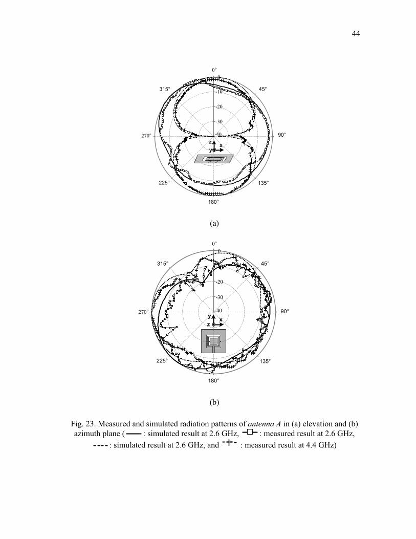
The normalized radiation patterns at the lower and higher operating frequencies
for Antenna A are presented in Figure 23. Measured and simulated results are matched
well with each other. The radiation patterns at 4.4 GHz in elevation plane are normal
loop antenna pattern as expected as shown in Figure 23(a). The main beam of 2.6 GHz
in elevation plane is tilted a little to the direction of -20o. Possible reason could be that
currents around CSRRs are not symmetric since two slits on the CSRRs are not located
on symmetric positions. In azimuth plane shown in Figure 23 (b), the radiation patterns
at two operating frequencies are similar with each other. The unsymmetrical patterns are
due to slits on the CSRRs which leads unsymmetrical current flows on the patch. The
antenna gains were also measured, and the results are presented in Figure 24. From the
results, it is seen that the peak antenna gain at lower operating frequency is about 4.7 dBi.
Also, the peak antenna gain at higher operating frequencies is about 2 dBi. The higher
gain at the lower band is considered as the CSRR effects. The fabricated CSRR antenna
is shown in Figure 25.
4. Summary
A compact dual-frequency antenna using complementary sprit ring resonators is
presented and studied. The CSRR antenna is fed by coplanar waveguide. The
dimensions of the rectangular CSRRs are tuned to achieve dual band frequency
properties. The higher resonant frequency is dominantly determined by the outer slot
44
z
yx
-40
-30
-20
-10
0
0°
315°
270° 90°
45°
180°
225° 135°
(a)
-40
-30
-20
-10
0
0°
315°
270° 90°
45°
180°
225° 135°
z
yx
(b)
Fig. 23. Measured and simulated radiation patterns of antenna A in (a) elevation and (b)
azimuth plane ( : simulated result at 2.6 GHz, : measured result at 2.6 GHz,
: simulated result at 2.6 GHz, and : measured result at 4.4 GHz)

45
-8
-6
-4
-2
0
2
4
6
Frequency [GHz]
2.2 2.4 2.6 2.8 3.0
Gain
(dB
i)
(a)
-8
-6
-4
-2
0
2
4
Gain
(d
Bi)
Frequency [GHz]
4.0 4.2 4.4 4.6 4.8
(b)
Fig. 24. Measured gains of the proposed antenna at (a) 2.6 GHz and (b) 4.5 GHz

46
Fig. 25. The fabricated CSRR antenna
ring while the lower resonant frequency is generated by the coupling between two slots
rings, which are CSRRs. The proposed antenna achieves about 35% size reduction effect
at the low resonant frequency. The proposed inspired metamaterial antenna has
measured gains of 4.7 dBi and 2 dBi at 2.6 GHz and 4.5 GHz, respectively.

47
CHAPTER V
HIGH GAIN RECTIFYING ANTENNA
1. Introduction
Space solar power transmission (SPT) and microwave wireless power
transmission (WPT) have been attracted not only for an alternative solution to world
energy problems in the future, but also for morden commercialized uses such as radio
freqeuncy identification charger, or battery or power line free devices. The recteifying
antenna called rectenna is one of the most key components in the SPT and WPT system.
Among many technical developments in WPT history, the rectenna technologies have
been dominantly improved for the system performance and efficiency improvement
[18],[64], and[65].
Traditionally, dipoles or dipole-like antennas are used in rectenna design [66].
the coplanar stripline (CPS) is normally used to feed the antenna in a rectenna system
due to easy fabrication and high characteristic impedance [28],[67],and[68]. In recent
years, several different type of rectenna with differnet performances have been reported.
A harmonic-rejecting circular sector rectenna for avoiding filter sections in rectenna
circuits was reported [69]. A circularly polarized dual band rectenna was developed for
portable wireless device applications [70]. Another circular polarized rectenna with two
slot patch antennas was built for dual band performances: one resonant band is for data

48
communication and the other is for wireless power transmission [71]. To prevent the
output voltage variations due to improper mainbeam alignment, a non-uniform rectenna
array was proposed [72]. Another soultion to have constant output power is to use a
retrodirective array [73]-[75]. The automatic beam steering features have been widely
used in many wireless communication systems [76]-[78]. Retrodirective rectennas also
have been developed using bow-tie antenna and microstrip ring elements [79]-[80].
To provide high DC output power, the rectenna system needs to receive a large
amount of incoming RF power. To achieve this, high gain antenna element or a large
antenna array for high gain performance are necessary. In this chapter, the WPT system
and the rectenna operation theory are reviewed, and then a efficient high gain rectenna
with pentagon rings is presented.
2. Wireless Power Transmission System
The main difference between the WPT system and communication systems is
transferred power efficiency. Normally, the communication systems receive signals from
all directions when the transmitters diffuses the signalsn while the WPT systems focus
on a point reciever or pointed recievers for efficient wireless power transfer. So, even
though the received signals have enough power for communications, the efficency of the
communication system is very low comparing with the WPT system. Therefore,
efficency is critical factor in the design of the WPT system.
A WPT system consists of three main functional blocks as shown in Figure 26.
The first block is DC-to-RF transmitter. The original DC energy is converted to RF
energy and the converted RF are radiated in the first block. The original DC source is

49
Fig. 26. Wireless power transmission system schematic
collected by either photovoltaic cells or solar thermal turbines. The DC to microwave
convertor is either microwave tube (magnetron) system or simiconductor systems. The
antenna element or array antennas are used to radiate the RF energy. The efficiency (t)
of the first block, the electric to microwave conversion efficiency, is equal to the product
of magnetron efficiency (mag) and the array antenna efficiency (a). The magnetron
efficiency is used to express how efficient the RF source works. The antenna efficiency
at the transmitter represents the ability of the antenna to radiate the distributed RF power
fed from the RF source and radiated into free-space.
The second block is free space channel. The radiated RF power from the array
antenna is transferred across free space within a specific focused beam towards a
receiver. The efficiency (c) is this block, collection efficiency, is the ratio of the
received power over the transmitted power. For maximum collection efficiency, an
optimum power density distribution must be selected for the transmitting antenna
aperture. A non-uniformly illuminated aperture increases the collection efficiency and it
has been seen that the optimal taper is of Gaussian type. The collection efficiency is

50
proportional to a design parameter , which is expressed as Goubau‟s relation [81]-[82]
D
AA tr
0 (32)
where Ar and At are the aperture areas of the receiver and the transmitter antennas. As
can be seen from this equation, Goubau‟s relation can be used to determine the size of
the apertures involved. The collection efficiency is given by
%100)e1(2
c (33)
which is proportional to the power density and the incremental area of the antenna. For
example, as At becomes larger, the incident power density also increases leading to a
higher collection efficiency as seen through . This translates into a tradeoff between the
efficiency and the size.
The last block is RF-to-DC receiver, where rectennas rectify the incomming RF
signals to generate DC output power. Figure 27 shows the basic components of the
rectenna element. An antenna element attaches to a RF filter (bandpass or lowpass filter)
that transforms the impedance of the antenna to the rectifier impedance and prevents the
high-order harmonics resulted from the rectifier reradiating. The rectifying diode is the
Fig. 27. Rectenna block diagram

51
core element of the rectifier. The output DC filter of a large capacitor effectively shorts
the RF energy and passes the DC power. A load resistor is placed at the output terminal
to measure the DC output voltage. The efficiency of this block is called rectenna
efficiency.
The overall efficiency (all) of a WPT system is the ratio of the DC output power
at the receiver end over the DC (or RF) input power at the transmitter end, which is
given by
rctall (34)
which means that the end-to-end efficiency includes all the sub-efficiencies starting from
the DC supply feeding the RF source in the transmitter to the DC power interface at the
receiver output.
3. Rectenna Operation Theory
It is important to understand how a half-wave rectifier with shunt capacitor
works, which is the fundamental theory used for a microwave rectenna design. The basic
theory of the half-wave rectifier can be found in [83]. The rectenna operation theory has
been studied in [67]-[68]. In this chapter, several important concepts are reviewed.
A. Rectifying Circuit Theory
The rectenna circuit consists of the half-wave rectifier circuit and the DC-pass
capacitor where the capacitor is in shunt with the diode as shown in Figure 28 (a). The
voltage across the load as a function of time is

52
+
-
VD C
+
-
v D RL
v D
= Vpcoswt
+
-
i D
(a)
Vmax
Vmin
v S, v L
ON OFF ON OFF ON
v S
v L
T
t
(b)
Fig. 28. (a) Half-wave rectifier with capacitor and (b) its waveforms
( ) ( )0 0 L L
t t
R C R C
L P Pt V e V e
(35)
where RLC is the time constant, VP is the initial value and 0 is the final voltage if the
capacitor completely discharges. The time t is measured from the peak where the voltage
is equal to VP. When the rectenna‟s operating frequency has such a short period in
comparison with the RLC time constant, the exponential decrease in the voltage can be
approximated by a straight line as shown in Figure 28 (b).
By series expanding, equation (35) becomes

53
( )
2
1 ...2
L
t
R C L
L P P
L
t
R Ctt V e V
R C
(36)
Since the decreasing voltage has been approximated as a straight line, the linear terms of
the equation (36) are kept and the minimum voltage at t = T becomes
min
11 1P P
L L
TV V V
R C fR C
(37)
Once the diode voltage drops to Vmin, the diode turns on and the voltage again
approaches Vmax = VP. The peak-to-peak ripple of the voltage waveform is
max minP
r
L
VV V V
fR C (38)
and the average DC diode voltage present across the load resistor is
max min 11
2 2D P P
L
V VV V V
fR C
(39)
The period of the incoming 5.8 GHz energy is 172.4 ps. The capacitance of the DC-pass
filter is approximately 2400 pF. This translates to RLC >> T. Therefore, the ripple
voltage Vr is very small, and the average diode DC voltage is VD VP. This average DC
diode voltage is also known as the self-bias voltage used in further analysis.
B. Diode Modeling
Figure 29 shows a RF voltage waveform operating across the diode and the diode
junction voltage. This model assumes the harmonic impedances seen by the diode are
either zero of infinite that avoids the power loss by the harmonics. The fundamental

54
voltage wave will not be corrupted by the higher order harmonic components. Then the
rectenna conversion efficiency only depends on the diode electrical parameters and the
circuit losses at DC and the fundamental frequency. The voltage waveform can be
expressed as
( )cosV V V tI D P
(40)
2 on
Vbr
Vbi
I
V
on
n
VI
Vj
VP
VD
Vj1
Vj0
Phase
Fig. 29. Diode current-voltage characteristic curves with the incident fundamental and
diode junction voltage waveforms

55
where VD is the self-bias DC output voltage across the resistive load RL, and VP is the
peak voltage amplitude of the incident RF power. The rectifying diode acts as a mixer
that produces a self-bias voltage. As the incident power is increased, the rectified self-
biasing will become more reversed biased. The diode junction voltage is
( )cos ,0 1
,
V V t V Vjj j biV j V V Vjbi bi
(41)
where Vj0 and Vj1 are the DC and fundamental frequency components of the diode
junction voltage, respectively; Vbi is the diode‟s built-in turn-on voltage; on is the
forward bias turn-on angle. When the junction voltage exceeds Vbi, the diode will
operate in forward conduction. Figure 29 also shows that the diode‟s junction waveform
slightly lags the incident power by a phase difference .
The equivalent circuit used to determine the diode‟s efficiency is shown in Figure
30. The diode parasitic reactive elements are excluded from the circuit. The diode model
consists of a series resistance RS, a nonlinear junction resistance Rj, a non-linear junction
capacitance Cj, and a load resistor RL. The junction rsistance Rj is assumed to be zero for
forward bias and infinite for reverse bias. Applying Kirchoff‟s voltage law in the
equivalent circuit, we have
0,
V I R VD D S j dc
(42)
With VD = IDRL, the DC output voltage is given by
,
RLV V
D j dc R RLS
(43)

56
RL
ID
RS
VI
Rj C
jV
j
VD
I
Fig. 30. Equivalent circuit model of the half-wave rectifier
The DC output voltage is determined from the rectified voltage across the diode junction
Vj. In each cycle, the average value of Vj is
( )2
1 1 dθ cos dθ
0 1, 2 2
on onV V V V
j jj dc bion on
(44)
The first term and the second term represent the forward-biased and the reverse-biased
cases. Integrate the equation gives
11 sin
0,
Vjon onV V V onjj dc bi
(45)
When the diode switches from off to on, Vj = Vbi. Then we have
cos0 1
V V Vonj j bi (46)
When the diode is off, Rj is infinite. Applying Kirchoff‟s voltage to the other loop gives
0V IR V jI S (47)
with

57
dC Vj jI
dt (48)
These two equations can be rewritten by
( ) ( )d C V V Vj j jI
dt RS
(49)
where Cj can be expressed as a harmonic function of VD
( ) ( )cos cos 2 2 ...0 1 2
C C C t C tj (50)
Using above two equations yields
( ) ( )sin cos cos sin sin1 0 0 1 0 1
R C V C V V V V V VD P PS j j j j
(51)
where = t - . Because this equation also holds for the off period, each sinusoidal
term can be collected as
0V V
Dj (52)
cos1
V VPj
(53)
( )sin1 0 0 1
V R C V C VP S j j
(54)
Substituting (52) to (45) and inserting (43) into (45) obtains
11sin 1
V VR jS on bion
R V VL D D
(55)
It can be shown that the phase difference can be approximated to be zero, which
results in VP = Vj1. Inserting this and (52) into (46) and (55) to obtain

58
tan
1
RS
on onV
biRL V
D
(56)
This transcendental expression allows obtaining on iteratively, which is dependent on
the diode input power that determines both Vbi and VD.
The diode efficiency can be expressed as
Pdc
D P PL dc
(57)
where PL is the power dissipated by the diode and Pdc is the DC output power across RL.
They are given by
, , ,P L L LL on R off R on diode
S S (58)
2VoP
dc RL
(59)
The three terms of the diode loss PL can be expressed by
( )2
1, 2
V Von I biL don R RS on S
(60)
( )2
21
, 2
V Von I dL doff R RS on S
(61)
( )1
, 2
V V Von I bi biL don diode R
on S
(62)
Since it is assumed the junction resistance is infinite during the off cycle, the loss

59
through the diode junction has been neglected. These power losses are the time-average
products of the current flowing through an element and the voltage across the element.
The total power dissipated on the series resistance can be solve by integrating
( ) ( )2221 2cos sin
2
on onL V V V d R C V djR D P PSbiRS on onS
(63)
Using the RF current instead of voltage in the second integral, (27) can be rewritten as
( ) ( )2 2
2 21 1
, 2 2
V V IRon onjI SL d doff R R RS on onS S
(64)
where I is the RF current flowing through the diode in reverse bias. It is assumed that no
current flows through Rj in reverse bias and all of the current flowing through RS flows
through Cj. Then (48) can be expressed as
dV jI C j dt
(65)
The voltage drop across RS is so small in the off cycle that the phase difference is set
zero. Apply this in (55) to obtain Vj1 = VP. Then
( )cos sin0
dI C V V t C Vj jP Pjdt
(66)
The power dissipated by the diode junction is rewritten as
( )1cos
2
onL V V V V d
D Pdiode bi biRonS
(67)
where VP is determined, while the diode is off, by

60
cos
V VD biV
Pon
(68)
Use the results from (63) and (68) and insert them into (57), we have
11D A B C
(69)
where
21 3
1 1 tan2 22cos
VRbiLA on on
R VD onS
(70)
2 2
1 tan22 cos
R R C VjLS bi onB onV
D on
(71)
( )1 tanV VR
bi biLC on onR V V
D DS
(72)
with = 2f. The diode junction capacitance is given by
0
VbiC Cj j V V
Dbi
(73)
where Cjo is the zero bias junction capacitance of the diode
The input impedance of the diode can be decided from the current I flowing
through RS in one cycle, that is
( ) ( )cos sin0 1 1
I I I t I tr i
(74)
where I0 is the DC component; I1r and I1i are the real and imaginary parts of the
fundamental frequency component, respectively. These current components are

61
( ) ( )2
10 2
on onI V V d V V djI IbiR
on onS
(75)
( ) ( ) ( ) ( )2
1cos cos
1
on onI V V d V V djI Ir biR
on onS
(76)
( ) ( ) ( ) ( )2
1sin sin
1
on onI V V d V V djI Ii biR
on onS
(77)
The diode input impedance at the fundamental frequency is
1 1
VPZ
D I jIr i
(78)
Assume that there is no current flow through Cj during forward bias and that all current
flow through during reverse bias, the diode current in one cycle can be found by
integrating
( )2
1 2cos cos sin1 1
C Von onj PI jI V V V d j d
D Pr i biRon onS
(79)
The second integral is solved similar to that in (63). Then the diode input impedance can
be written as
cos sin sincos cos
RSZ
Don onj R Con on onjS
on on
(80)
If the reactance of the diode impedance is tuned out by using the impedance matching,
the diode input impedance can be rewritten as

62
on
on
onon
SD
RR
sincos
cos
(81)
The input resistance is a dynamic variable dependent on the input power, as the same as
the diode efficiency.
4. High Gain Rectenna Element Design
The proposed high gain rectenna is shown in Figure 31. The rectenna is
comprised of a pair of pentagonal loop antennas, a detector diode in shunt, a capacitor in
shunt, and a load at the end of the rectenna system. The coplanar stripline fed pentagonal
loop antennas are designed to achieve high gain and high radiation effciency. The main
role of the antenna is to receive the RF signals effectively from free space. Unlike
normal rectenna designs, this rectenna element does not include a band-reject filter
which is for suppression of harmonics generated from a rectifying diode. The RF signals
passed the diode are converted into DC power. The capacitor next loacted to the diode
works as DC pass filter. It does not only block RF singals traveling toward the resistive
load, but also tune out the reactance of the diode. Finally, the proper value of the
resistive load is selected to maximize output DC power. To optimize the rectenna
performance, proper placement of the diode and the DC pass filter should be carefully
considered.
A. Pentagonal Loop Antenna
The proposed antenna has a linearly polarized high gain characteristic which is

63
RL
+
-VDC
DC- pass filter
Rectifying
Diode Resistive Load
Pentagonal Loop
Antenna
h2
Front view of CPS structure
air layer
εr1
εr2=1
h1
w wg
Impedance
TransformerTunning
Stub
LS LA
ZAZD
Lp
Wp
Fig. 31. Configuration of the proposed high gain rectenna with pentagonal loops.
demanded for rectenna systems. The two pentagonal loops with the same size are based
on coplanar stripline feed. The antennas printed on the substrate RT/Duroid 5880 with
20 mils (h1) thickness. A reflecting conducing plane is placed 11.2 mm (h2) behind the
substrate to achieve a higher gain by directing the beam broadside in one direction, and
reduce the back-radiation. The antenna parameters are optimized for 5.8 GHz frequency
operation by using the IE3D simulator, an electromagnetic full-wave analysis software
based on Method of Moment. The optimized dimensions are Lp = 12.7 mm, LS = 14.76
mm, LA = 11. 41 mm, Wp = 0.85 mm. With these values, the antenna achieves high gain
of 10.2 dBi at 5.8 GHz. Figure 32 and 33 show the simulated input impedance and gain
of the antenna. The antenna input impedance ZA is equal to 112 Ω. For antenna design in
a rectenna system, the input impedance of the antenna should be matched with input

64
Frequency (GHz)
5.0 5.1 5.2 5.3 5.4 5.5 5.6 5.7 5.8 5.9 6.0 6.1 6.2 6.3 6.4 6.5-100
-50
0
50
100
150
200
250
300
Re
(Zin
) &
Im
(Z
in) Re (Zin) = 184
Im (Zin) = 7.2
Fig. 32. Simulated input impedance of the antenna
5.0 5.1 5.2 5.3 5.4 5.5 5.6 5.7 5.8 5.9 6.0 6.1 6.2 6.3 6.4 6.5-10
-5
0
5
10
15
Gai
n (
dB
i)
Frequncy (GHz)
Fig. 33. Simulated antenna gain

65
impedance of rectifying diode circuit.
B. Coplanar Stripline Structure
The proposed rectenna is based on coplanar stripline structures as shown in
Figure 31. The dimensions of the CPS in both antenna feed and the rectifying circuit are
w = 0.9 mm and g = 0.4 mm. The characterisitic impedance of the CPS is 184 Ω.
Another CPS structure is located between the antenna and the diode as an impedance
tranformer. To obtain optimizing maching network, the CPS is designed with w = 1.92
mm and g = 0.4 mm for 143.5 Ω of characteristic impedance. Therefore, the input
impedance ZD before the diode becomes 184 Ω. In rectenna design, the characterisitic
impedance of the based transmission line is chosen to match the impedances of the
antenna with the diode to reduce the signal reflections between these components.
C. Detector Diode and DC Pass Filter
The diodes used in this dissertation are the GaAs flip chip Schottky barrier
diodes (Model MA4E1317) from M/A COM. It has a series resistance RS = 4 , zero-
bias junction capacitance Cj0 = 0.02 pF, forward-bias turn-on voltage Vbi = 0.7 V, and
breakdown voltage VB = 7 V. The junction capacitance (Cj) of the diode, described in
(69), significantly affects the diode efficiency, which is a function of the diode output
voltage. Equation (69) is rewritten here for convenience
||0
Dbi
bijj
VV
VCC
(82)
VD is the output self-bias voltage of the diode. Higher VD results in a smaller junction

66
capacitance, which also gives better conversion efficiency. The maximum efficiency
occurs when Cj approaches to zero. Furthermore, the diode should operate as close to its
voltage limit as possible to minimize its reactance. This reduces the reflection of the RF
power at the diode terminal and hence increases the rectenna efficiency.
A broadband DC-blocking chip capacitor by Dielectric Laboratories (Model
C08BLBB1X5UX) is chosen as the DC pass filter. The DC pass filter not only tunes out
the reactance of the diode but also blocks the unwanted RF signals from reaching the
load resistance. The detector diode and the DC-blocking capacitor are mounted across
the coplanar stripline by using silver epoxy.
D. Rectenna Measurements and Conversion Efficieny
The free space measurement of the rectenna has been studied in [28]. The
equipment setup is shown in Figure 34. The RF-to-DC conversion efficiency of the
rectenna () can be defined as
r
DC
P
P (83)
PDC is the DC output power. Friis transmission equation is used to calculate the power
propagating to the CP antenna (Pr). A NARDA standard horn antenna with a 15 dB gain
(Gt) is used to transmit the RF power (Pt), and the rectenna gain (Gr) is set equal to 10.1
dB. By changing the distance between the horn antenna and the rectenna, the efficiencies
for different power densities are determined. The power density (Pd) is given by

67
HP 8341 B
Synthesized
Sweeper
46 dBm
(40 W)
Amplifier
Coax - 16 dB
Directional
Coupler
50
Power
Meter
Coax - 20 dB
Directional
Coupler
2
13
Linearly Polarized
Narda 642
Standard
Gain Horn
Gt = 15.1 dB
Gx,y
(x,y,s)
s
x
y
(0,0)
Path Loss 1 to 2 = 41.5 dB
Path Loss 1 to 3 = 0.86 dB
Incident Energy
(not a plane wave)
VA
RA
Voltmeter
Circularly Polarized
Rectifying
Antenna
or
Arrayb
a
Fig. 34. Free space measurement setup of the rectenna
24 D
GPP tt
d
(84)
where D is the distance between the horn antenna and the center of the rectenna.
The conversion efficiency curves of the single high gain rectenna at 5.8 GHz are
shown in Figure 35. The best RF-to-DC conversion efficiency of the rectenna is 75 %
when the load and the DC output voltage are 100 and 5.4 V, respectivley. It is
obviously seen that the efficiency gradually decreases as the load resistance increases.
5. Summary
In this chpater, WPT system and rectenna operation theory have been reviewed.
A pentagonal loop antenna has been developed at 5.8 GHz. The pentagonal loop
provides linear polarization and achieves high gain of 10.1 dBi. The CPS feed line is

68
Power density (mW)
0 5 10 15 20 25 30
Co
nv
ersi
on
eff
icie
ncy
(%
)
10
20
30
40
50
60
70
80
R =100
R =150
R= 250
Fig. 35. Measured rectenna efficiency at 5.8 GHz
designed with characteristic impedance of 184 . A impedance transfermer is used to
match the antenna input impedance to the diode input impedance. The proposed rectenna
achieves a maximum conversion efficiency of 75% with the resistivie load of 100 .

69
CHAPTER VI
RECTIFYING ANTENNA ARRAY USING REFLECTARRAY
1. Introduction
In the past, several array types of rectennas have been studied with high gain
property to achieve a long distance WPT, higher output DC power, and reduced
receiving areas. However, in the array rectenna design, there might be several problems,
such as: the relatively high loss of array feeding networks, difficulty in feeding network
design, and antenna coupling between the nearest located radiators thus causing lower
rectenna array performance. To overcome these downsides, a novel rectenna system
using a reflectarray instead of array antenna elements is proposed in this chapter.
The reflectarray combines the advantages of both traditional reflector antennas (the
most often used high gain antennas) and conventional phased array antennas, such as:
being flat, having a low-profile, and being easier to manufacture. Moreover, the spatial
feeding method eliminates the energy loss and design complexity of the conventional
feed networks. The reflectarray features can be adapted to a rectenna for the WPT
system. The reflectarray normally achieves high gain that a feed network is not
necessary, nor is an antenna coupling. The proposed novel rectenna array suggests a new
type of long distance WPT system.

70
2. Reflectarray Operation Theory
A. Basic Reflectarray Operation Theory
The basic operation theory of the reflectarray is reviewed from the reference [84].
Figure 36 shows the geometry of a microstrip reflectarray and the image of a parabolic
reflector. A feed antenna is placed at the focal point to illuminate the reflectarray. When
the wave from the feed antenna is incident on the reflectarray surface, the elements of
the reflectarray will reradiate the incident energy into the space. However, as can be seen
from Figure 36, the incident path lengths for the field propagating from the feed antenna
to the elements are different. Therefore, the reradiated field will not be coherent.
The key to the reflectarray design is to adjust the reflection phases of the elements
to compensate for the path length differences so that the reradiated fields from each
element would be collimated towards one specific direction. The analysis is derived by
comparing the configurations of a parabolic reflector and a flat microstrip reflectarray.
Figure 37 shows the block diagram of a flat reflectarray with its virtual parabolic
surface. An incident plane wave strikes the parabolic reflector‟s metal surface and
bounces to a focal point a distance f above the center of the parabolic reflector. Each
reflectarray elements are located at a position (x’,y’) from the center of the array (0,0).
The distance between the focal point and any antenna element is denoted as rmn. The
angle θ’ is the angle between the path connecting the focal point and the array center and
the path connecting the focal point and the antenna element.

71
Reflectarray
Parabolic reflector image
Feed antenna
Fig. 36. Geometry of a microstrip reflectarray
(x’, y’)
(0, 0) a
Fig. 37. Reflectarray block diagram

72
The dimension of the reflector (d) and the largest angle (θ0) from the center of the
parabolic reflector to its edge are related [86] as
1
0 2
0.5
tan1
16
f
d
f
d
(85)
From equation (85), the diameter of the reflectarray can be determined by
( )02 tanrd f (86)
The angle θ’ can also expressed as
'2 '2' 1tan
x y
f
(87)
The distance from the focal point to any point on the surface of the parabolicreflector is
[85]
'
'
2
1 cos
fr
(88)
For any angle θ’, the distance from the reference plane to the reflectarray to the
focal point is (s + s cos θ’) longer than the corresponding ray trace from the reference
plane to the parabolic dish to the focal point. This additional path length must be
compensated in the design of the reflecting element array in order to provide the
parabolic phase front across the surface of the array. The path length in radians is
'0
'
2( cos )
fs s
c
(89)

73
where f0 is the resonant frequency of the array and c is the light speed. The distance s is
equal to
'
'cos
fs r
(90)
The antenna elements are designed properly to compensate for the additional
path lengths Δl.
B. Aperture Efficiency of Reflectarray
In the design of a reflectarray system, the aperture efficiency is one of the most
important factors to predict the reflectarray system performance. Similar to the normal
parabolic reflector, the design of the reflectarray system usually begins with a specified
gain. The gain of a reflectarray antenn can be obtained by the product of the aperture
directivity and the aperture efficiency. The aperture directivity Dr is determined by the
aperture area A as
2
4r
AD
(91)
Then , the gain of the reflectarray antenna is defined as
2
4a
AG
(92)
If the aperture efficiency does not include the efficiency factors related with the feed loss,
reflectarray element loss, polarization loss, and mismatch loss, the aperture loss is
determined by two dominant efficiency terms in the reflectarray design: the spillover
efficiency (ηs) and the illumination efficiency (ηi). So, the aperture efficiency can be
defined as

74
a s i (93)
To calculate the efficiencies of the reflectarray, the radiation properties of the
feed antenna should be modeled. Among various radiation models, cosq pattern is used
in this study due to its simplicity.
2cos (0 )2
q
fU
(94)
The parameter q determines the pattern shape and the directivity of the feed antenna.
Figure 38 shows the directivity of the feed antenna versus the q value. The large q value,
the higher directivity is. Once the feed antenna is designed with a specific directivity, the
q value is obtained.To verify the cosq pattern, Figure 39 shows the real antenn pattern
with 10 dBi of directivity and cosq pattern with 2 of q value. As seen from the result, two
patterns are matched well with each other.
The term spillover is defined as the ratio of the power intercepted by the
reflecting elements to the total power, which is usually considerd in transmit mode.
Figure 40 shows the reflectarray configuration for spillover efficiency, which is the
percentage of the radiated power from the feed that is intercepted by the reflecting
aperture [86].
( )
( )s
total
P r s
P r s
(95)
where the denominator is the total power radiated by the feed, and the numerator is the
portion σ of the power incident on the array apperture.

75
q
0 2 4 6 8 10
dir
ecti
vit
y(d
B)
2
4
6
8
10
12
14
16
18
Fig. 38. Directivity vs. q factor of the feed
Angle
-40 -30 -20 -10 0 10 20 30 40
Po
wer
lev
el(d
B)
0.0
0.2
0.4
0.6
0.8
1.0
Fig. 39. The real antenna pattern vs. cosq pattern
( : real antenna pattern, : cosq pattern)

76
The spillover efficency in equation (95) can be expressed in terms of the design
parameters of the reflectarray system [86] as
22 /2 2 2 2
0
3
00 0
2 1
2 2
qD
s
q H r r sd
r r r
(96)
Thus, ηs is a function of six design parmaters:
0 0 0( , , , , , )s s D H q x y (97)
From the result, the spillover efficiency is free from the reflectarray element pattern
among all the configuration parameters.
D
Feed antennay
x z
F
Fig. 40. Reflectarray configuration for spillover efficiency
The illumination efficiency is efficiency loss due to non-uniform amplitude and
phase illumination of the aperture plane.

77
2
2
( , )1
( , )
A
i
a
A
I x y dA
A I x y dA
(98)
where I(x,y) is the amplitude distribution over the aperture. This can be also calculated
[86] as
22 /2 2 2 2
0
1
00 0
2 2 /2 2 2 2
0
1
00 0
1
24
1
2
qD
e
i qD
e
r r sd
r q r r
D r r sd
r q r r
(99)
which means that ηi is a function of seven parameters:
0 0 0( , , , , , , )i i eD F q x y q (100)
The aperture efficiency of the reflectarray can be calculated once the spillover
efficency and illumination efficiency are determinded.
0 0 0( , , , , , , )a i s eD F q x y q (101)
In the design of a reflectarray, it is desired to find the maximum aperture
efficiency with the given design parameters. Especially, the feed location is an important
parameter in practical design. The feed location is described by the offset angle θ0 and
the height F.
Figure 41 shows the aperture efficiency versus the ratio of the feed height F to
reflectarray diameter D. In this study, the offset angle θ0 is set at 25o. As F/D grows, the
maximum aperture efficiency appears at the higher q factor value. For example, if the

78
gain of the feed antenna is set 10 dBi, which means the q factor value is about 2, from
the graph, the aperture efficiency of the reflectarray is expected as 60 % with F/D of 0.6.
Figure 42 shows efficiencies versus q value with F/D of 0.6. It is seen from the results
that as the value q increase, the spillover efficiency increases and the illumination
efficiency decreases. The aperture efficiency reaches a maximum when q is equal to 0.66
in this study.
As a result, the aperture efficiency is affected by the following reflectarray
parameters: the shape and dimensions of the aperture, the position of the feed, the
direction of the feeding beam, the pattern of the feed, and the pattern of the reflectarray
elements.
3. Reflectarray Component Design
In this chapter, a compact reflectarray element is desinged for a rectifying
reflectarray system. The configuration of the proposed reflectarray is shown in Figure 43.
This reflectarray elements are printed on the substrate Rogers RT/5880 with thickness of
0.508 mm. The air form layer (εr = 1.06) of 3.2 mm is inserted between the substrate and
the ground plane. The unit cell element with its dimensions and the close-up picture of
the reflectarray elements are shown in Figure 44. The proposed element is a combination
of an inner circular patch and an outer ring with ring radius and width of R and Wr,
respectively. In the element design, outer ring width Wr and gap width Wg is fixed as 1
mm and 0.5 mm, respectively. The important design parameter is radius of the outer ring
R which is varied to obtain the element reflection phase variation curve.

79
q factor of the feed
0 2 4 6 8 10 12 140.2
0.3
0.4
0.5
0.6
0.7
0.8
0.5
0.6
0.7
0.8
0.9
1.0
F/D Eff
icie
ncy
Fig. 41. Aperture efficiency vs. F/D
0 2 4 6 8 10 12 14
0.4
0.5
0.6
0.7
0.8
0.9
1
Illumination efficiency
Spillover efficiency
Total efficiency
q factor of feed pattern
Effic
ien
cy (
%)
Fig. 42. Efficiency vs. F/D

80
The unit cell size is 18 mm X 18 mm, which is 0.35 λ0 X 0.35 λ0 at 5.8 GHz. The
compact size unit cell allows more elements to be added in the limited area, which leads
to have higher gain. Figure 45 shows the simulated reflection phases against the unit cell
element by controlling the outer ring radius R at the operation frequency. Neither the
ring nor the circular patch alone can provide a sufficient phase variation range for a
practical reflectarray design. With the proposed ring-patch combination, it is found that
the compact reflectarray element provides a sufficient phase range of 370o.
Air foam
0.508 mm
3.2 mm
Reflectarray
element
Ground plane Substrate RT/Duroid 5880
Fig. 43. 3D configuration of the reflectarray

81
R
Wr
Wg
Outer ring width: 1 mm
Gap width : 0.5 mm
0.35 λ0
Unit cell
Fig. 44. Unit reflectarray element and its picture
Radius of the outer ring R (mm)
4 5 6 7 8 9
Ref
lect
ion
Ph
ase
(Deg
ree)
-450
-400
-350
-300
-250
-200
-150
-100
-50
0
Phase variation = 370o
Fig. 45. Phase variation of the unit cell element

82
4. Rectifying Reflectarray
A novel rectenna array using a reflectarray which is called “rectifying
reflectarray” here is presented in this chapter. The difference from the conventional
reflectrarrays is that the feed antenna of a reflectarray is replaced with a rectifying
antenna to generate DC energy. The rectenna with high gain property presented in the
Chapter V and the reflectarray proposed with compact unit cell in this chapter are
combined into a novel rectifying reflectarray.
Figure 46 shows the feed antenna designed to measure the gain of the reflectarray.
The antenna component is the same with the antenna in the high gain rectenna circuits
except the connected balun, instead of a rectifying circuit. The foam layer inserted
between substrate and ground plane is not filled by a foam, but is supported by four
plastic screws, which make thickness of the layer controllable. The measured radiation
patterns of the feed antenna are shown in Figure 47. The maximum gain point is shifted
slightly to – 7o. The shift could be due to that the balun makes current flow on the
antenna unsymmetric. Maximum gain of the antenna in elevation plane is 10.2 dBi.
The reflectarray is measured with the pentagonal loop antenna located at focal
point as shown in Figure 48. In the reflectarray design, q factor is 2 for the feed gain of
10 dBi and F/D is set by 0.6. So, almost 60 % maximum aperture efficiency is expected
from the reflectarray theory. To avoid incident field blockage, the reflectarray has the
offset feed with θ0 = 20o.

83
(a) (b)
Fig. 46. Feed antenna: (a) top view and (b) side view
-30-90 90
-22
-14
-5
3
11
-45 45
0
Fig. 47. Measured radiation patterns of the feed antenna in elevation plane

84
Fig. 48. Reflectarray with the feed antenna
Angle (degrees)
-180 -150 -120 -90 -60 -30 0 30 60 90 120 150 180
Gai
n (
dB
i)
-20
-15
-10
-5
0
5
10
15
20
25
Fig. 49. Measured radiation pattern of the reflectarray at 5.8 GHz

85
The measured radiation pattern of the reflectarray at 5.8 GHz is shown in Figure
49. The main beam is at broadside and the 3 dB beam width is about 11o . The peak
sidelobe level relative to the main beam is 16.2 dB. The maximum gain of the
reflectarray is 21.5 dBi, which is expected value from the reflectarray space
configuration information.
Figure 50 shows the rectenna for the proposed rectifying reflectarray design. The
rectenna is described in the Chapter V. The measured conversion efficiency curves of
the rectifying reflectarray are shown in Figure 51. Like the single antenna case, the
reflectarray rectenna achieves the maximume conversion efficiency of 71o when the
resistive load is 100 . The conversion efficiency of 150 load shows similar efficency
results with the 100 case. As the load resistance value increase, the efficiency
gradually decreases.
5. Summary
Basic operation theory of the reflectarray is reviewed. Several efficiency terms
are proposed, analyzed and derived to obtain the aperture efficiency of the reflectarray.
Based on the design theory, a reflectarray with compact unit cell elements has been
developed. The antenna component is measured with a balun and acheives 10.2 dB
maximum gain. The reflectarray is measured with the feed antenna to check the gain of
the reflectarray. The maximum gain is 21. 4 dBi. The proposed rectifying reflectarray
with the rectenna located at the focal point is measured with several load resisters and
achieved 71 % maximum conversion efficiency.

86
(a) (b)
Fig. 50. Rectifying antenna: (a) top view and (b) side view
Power density (mW)
Co
nv
ersi
on
eff
icie
ncy
(%
)
0 5 10 15 20 25 300
10
20
30
40
50
60
70
80
R =100
R =150 R= 250
Fig. 51. Measured conversion efficiency of the rectifying reflectarray

87
As the first prototype of the reflectarray rectenna, the results are reasonable.

88
CHAPTER VII
MICROWAVE APPLICATIONS: WIDEBAND COPLANAR
STRIPLINE TO DOUBLE-SIDED PARALLEL-STRIP LINE
TRANSITION AND DUAL BAND OMNI-DIRECTIONAL
ANTENNA FOR POLARIZATION DIVERSITY*
1. Introduction
A. Wideband Coplanar Stripline to Double-Sided Parallel-Strip Line Transition
The transition is a component to transfer electromagnetic energy from one type
to another type of transmission line structure. As modern microwave systems have been
demanded to be more complex and integrated with other types of components, the
transition is considered a key element for optimal performance of the system. The
transitions can be divided into two categories for the type of two transmission lines:
balanced to balanced line transitions and balanced to unbalanced line transitions. The
latter is especially called baluns. These transitions are used to feed CPS printed antennas
and build baluns for balanced mixers, balanced amplifiers and antennas in many
microwave applications.
______________
*Parts of this chapter are reprinted with permission from C.-H. Ahn and K. Chang, “Wideband coplanar stripline to double-sided parallel-strip line transition,” IET Electronics Letters, vol. 45, pp. 748-749, Jul. 2009. Copyright 2009 IET. The original version of this work is available at IET Digital Library; C.-H. Ahn, S.-W. Oh, and K. Chang, “A dual-frequency omnidirectional antenna for polarization diversity of MIMO and wireless communication applications,” IEEE Antennas and Wireless Propagation Letters, vol. 8, pp. 966-969, Aug. 2009. Copyright 2009 IEEE. For more information go to http://thesis.tamu.edu/forms/IEEE%20permission%20note.pdf/view.

89
Double-sided parallel-strip line (DSPSL) is a new balanced transmission line
with the advantage of good balanced performance, simple structure for wide-band
transitions, and ability to realize various characteristic impedances and large
capacitances due to its thin space between two conductors [87]. Recently, DSPSL has
been actively studied for many microwave applications such as transitions [87], filters
[88] and power dividers [89]. The coplanar stripline (CPS) is another attractive balanced
line structure. The characteristics of the CPS are low loss, small discontinuity parasitics,
and small dispersion, and simple implementation of open/short ended strips [90]. CPS
can be used to mount the solid-state components in series or shunt without via holes. The
uniplanar transmission line has been used in a number of applications such as antenna
feedings, rectennas, filters, and optoelectronic devices. Many microstrip line to Coplanar
waveguide (CPW) have been reported [91]. Wideband microstrip line to CPS transitions
have been studied [92]. Broadband DSPSL to CPW transition has been also investigated
[93]. However, no transition between CPS and DSPSL has been reported yet for two
attractive balanced lines, the CPS and DSPSL. In this chapter, a wideband CPS to
DSPSL transition is proposed for the first time. The characteristic impedance of CPS and
DSPSL is 148 Ω and 50 Ω, respectively. The proposed back-to-back transition operates
from 2.4 GHz to 10.7 GHz with the return loss of better than 10 dB and an insertion loss
of better than 2.5 dB. It has simple structure and can be easily fabricated. The transition
can be applied for many microwave applications.

90
B. Dual Frequency Omni-directional Antenna for Polarization Diversity
Wireless communication systems have been increasing rapidly for the last
several years. Multiple-Input Multiple-Output (MIMO) technology has been used to
improve wireless system performance because of its significant channel capacity and
capability to offer multiple functions. For achieving better communication performance
in specific areas, it has been considered important to determine a suitable diversity
technique for MIMO system. Polarization diversity has been studied as an optimized
MIMO technique for especially high multipath communication areas in substitute for
space diversity, which needs at least ten wavelength spacing between two receiving
antennas [94]. Polarization diversity system normally consists of two polarized antennas,
which should have orthogonal polarization with the same radiation patterns of each other
and high polarization purity for maximizing its capacity. A typical pair of the
orthogonally polarized antennas is vertically polarized dipole and horizontally polarized
magnetic dipole antenna. For lower frequency ranges, horizontally polarized small loop
antennas may be the proper choice as a magnetic dipole. Its short total length, less than
tenth of lamda, causes uniform current distribution on the surface, which leads to
omnidirectional radiation pattern [95]. However, due to its difficult impedance matching
condition, high reactance and small radiation resistance, the small loop antenna is not
suitable at higher frequencies. After the first Alford loop antenna in the wire type at a
high frequency was reported [96], several studies have been conducted using Alford loop
structure to generate magnetic dipole radiation patterns [97]-[100] instead of small loop
antennas. However, only single frequency horizontally polarization antennas have been

91
used so far. In this chapter, a novel printed dual-frequency Alford structure loop antenna
is proposed. The dual frequency operation is achieved without any extra matching
circuits or parasitic components. The horizontally polarized antenna consists of two
wing sections with different diameters, which are resonating at 2.45 and 3.9 GHz. The
effects of several design parameters of the proposed antenna are presented. The
measured return loss and radiation patterns are compared with simulation results using
HFSS design software, a 3D FEM based EM simulation. The proposed antenna could be
used as a good candidate of one polarized antenna of a pair of orthogonally polarized
MIMO system antennas.
2. Double-Sided Parallel-Strip Line
DSPSL has been analyzed first by Wheeler using conformal transformation
mapping method. The analyses show the closed-form equations derived for symmetrical
DSPSL separated by an air [101] and a dielectric layer [102]. However, by comparing
with conventional microstrip lines, the characteristics of the symmetrical DSPSL can be
found with less complexity using the symmetry. Figure 52 shows the configurations and
their electric field distribution of the double-sided parallel-strip line (a) and the
conventional microstrip line (b). The horizontal electric fields of symmetry in Figure 52
(a) generates zero potential plane located at Z = h/2 since the two conductors on top and
bottom are identical in magnitude and opposite in phase by image theory. The zero
potential plane can be considered as a virtual ground plane, which relates the

92
symmetrical DSPSL to the conventional microstrip lines. In Figure 52, the conductor
width of the DSPSL and the microstrip is the same as W. The substrate height of the
εr
W
2Cd
2Cdh
Ld/2
Ld/2
(a)
εr h/2
W
Cm
Lm
(b)
Fig. 52. Configurations of (a) symmetrical double-sided parallel-strip line and (b)
conventional microstrip line
DSPSL, and the micristrip line is 2h and h, respectively. According to the image theory,
it can be seen that the inductance per unit length of the DSPSL Ld is twice of that of the
microstrip line Lm, and the capacitance per unit length of the DSPSL Cd is one half of
that of the microstrip line Cm. Therefore, the characteristic impedance of the two cases
can be given by
2
2 2/ 2
d m mcd cm
d m m
L L LZ Z
C C C (102)
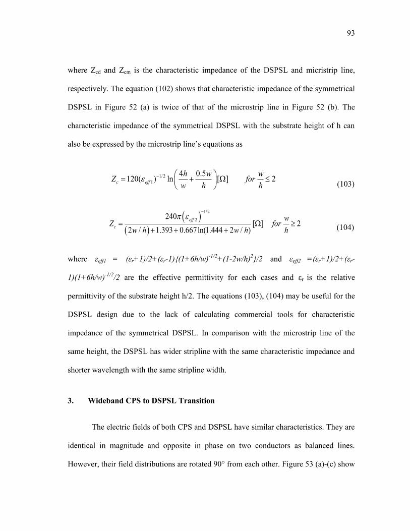
93
where Zcd and Zcm is the characteristic impedance of the DSPSL and micristrip line,
respectively. The equation (102) shows that characteristic impedance of the symmetrical
DSPSL in Figure 52 (a) is twice of that of the microstrip line in Figure 52 (b). The
characteristic impedance of the symmetrical DSPSL with the substrate height of h can
also be expressed by the microstrip line‟s equations as
1/2
1
4 0.5120( ) ln [ ] 2c eff
h w wZ for
w h h
(103)
( )( )
1/2
2240[ ] 2
2 / 1.393 0.667ln(1.444 2 / )
eff
c
wZ for
w h w h h
(104)
where εeff1 = (εr+1)/2+(εr-1)(1+6h/w)-1/2
+(1-2w/h)2/2 and εeff2 =(εr+1)/2+(εr-
1)(1+6h/w)-1/2
/2 are the effective permittivity for each cases and εr is the relative
permittivity of the substrate height h/2. The equations (103), (104) may be useful for the
DSPSL design due to the lack of calculating commercial tools for characteristic
impedance of the symmetrical DSPSL. In comparison with the microstrip line of the
same height, the DSPSL has wider stripline with the same characteristic impedance and
shorter wavelength with the same stripline width.
3. Wideband CPS to DSPSL Transition
The electric fields of both CPS and DSPSL have similar characteristics. They are
identical in magnitude and opposite in phase on two conductors as balanced lines.
However, their field distributions are rotated 90° from each other. Figure 53 (a)-(c) show

94
the configurations of the proposed double-sided parallel-strip line transition. The CPS
has electric fields formed across two conductor strips on top layer shown in Figure 53
(a). On the other hand, DSPSL produces vertical electric fields from conductor strips
located on top and bottom layer as shown separately in Figure 53 (b) and (c). The
proposed transition is designed to gradually change the electric fields of CPS mode to
those of DSPSL mode. The transition on top side is directly connected to both CPS and
DSPSL. That is, the width of one conductor of the transition on the top side is tapered
from the width of the CPS to the width of the DSPSL as shown in Figure 52 (b). The
conductor of the transition on the bottom side is electromagnetically coupled with one of
conductor of the CPS located on the top side. This bottom conductor of the transition is
tapered from the same location of the end part of the CPS in the z direction to the
conductor of the DSPSL as shown in Figure 53 (c). A radial stub at the end of the CPS is
designed for broadband coupling between the top and bottom conductors. Figure 54
shows the electric field distributions and cross sectional views at three different locations.
Figure 54 (a) shows CPS mode at A-A' location which has electric fields in the y-axis.
The horizontally distributed electric fields of the CPS mode are converted to the vertical
distribution in the DSPSL mode at C-C' location of Figure 54 (c), through the proposed
transition mode in the x and y – axis at B-B' location shown in Figure 54 (b). The
structures are all printed on substrate RT/Duroid 5870 with thickness (h) of 31 mil
(0.7874 mm) and a dielectric constant (εr) of 2.31. The 148 Ω characteristic impedance
of the CPS is determined by IE3D simulation with the strip width (W1) of the CPS of
3.5 mm, and the gap between two strips (g) of 0.8mm. The DSPSL width of the 50 Ω

95
characteristic impedance (W2) is 3.07 mm. The transition length (Lt) is 25 mm. The
angle (Ө) of the radial stub is optimized as 80° for good performance.
x
y
z
DSPSL
port
A
B
C
A'
B'
C'
CPS
TRANSITION
DSPSL
h
CPS
port
(a)
Top side
A
A'
B
B'
C
C'
g
Ɵ
W2
W1
(b)
Bottom side B
B'
C
C'
W2Lt
(c)
Fig. 53. Configurations of the proposed CPS to DSPSL transition: (a) 3D view, (b) top
side, and (c) bottom side

96
A - A'
εr substrate
(a)
B - B'
εr
(b)
C - C'
εr h
(c)
Fig. 54. Cross-sectional views of the proposed transition and electric field distributions:
(a) CPS mode, (b) Transition mode, and (c) DSPSL mode

97
S21
S11
Frequency [GHz]
2 4 6 8 10 12
S1
1 &
S2
1 [
dB
]
-30
-25
-20
-15
-10
-5
0
Measurement
Simulation
Fig. 55. Simulated and measured results of a CPS to DSPSL back to back
transition
The return loss and insertion loss of a back-to back transition were simulated and
measured using IE3D (a method of moment based EM simulator) and HP 8510 network
analyzer, respectively. Figure 55 shows the simulated and measured results of a CPS to
DSPSL back-to-back transition. The measured return loss of better than 10 dB and
insertion loss of better than 2.5 dB of the back-to-back transition are achieved from 2.4
GHz to 10.7 GHz. The 1.5 dB insertion loss bandwidth is obtained from 3.44 GHz to
5.74 GHz and from 6.64 GHz to 9.52 GHz. The insertion losses also include line
sections and discontinuities between the limited widths of the DSPSL and two coaxial
connectors for measurement purpose. The actual insertion losses for the transition are
lower.

98
4. Dual Frequency Omni-directional Antenna
The configuration of a dual frequency omnidirectional loop antenna (DOLA) is
shown in Figure 56. The current distributions on both the top plane and the bottom plane
are shown in Figure 56 (a) and Figure 56 (b). The waves on the cross-shaped double
sided strip lines are guided due to the opposite current directions on both sides. The eight
outer wing structures generate radiation fields caused by a uniform one direction current
distribution which causes omnidirectional radiation characteristics. Figure 56 (c) shows
a combined structure with the total current distributions. The two current distributions on
the wings generate two different omnidirectional radiation fields. The side view of the
proposed antenna is shown in Figure 54 (d). The proposed antenna is printed on
substrate RT/Duroid 5880 with thickness and a dielectric constant of 62 mil (1.57 mm)
TABLE 3. The design parameters of the dual band
Omni-directional loop antenna [unit:mm]
L1 L2 r1 r2 w t1 t2
19.0 8.4 23.7 10.8 1.9 0.4 0.0

99
r2
r1
W
L1
L2
W t2
t1
(a) (b)
er Inner conductor
Top plane
Bottom plane
xy
z
(c) (d)
Fig. 56. (a) Top plane conductor and its current distributions, (b) bottom plane conductor
and its current distributions, (c) top view of the combined antenna and current
distributions, and (d) side view of the proposed antenna
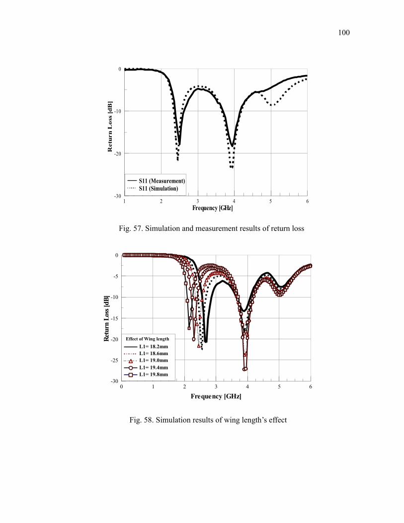
100
Frequency [GHz]1 2 3 4 5 6
Retu
rn
Lo
ss [
dB
]
-30
-20
-10
0
S11 (Measurement)
S11 (Simulation)
Fig. 57. Simulation and measurement results of return loss
Frequency [GHz]
0 1 2 3 4 5 6
Ret
urn
Loss
[d
B]
-30
-25
-20
-15
-10
-5
0
Effect of Wing length
L1= 18.2mm
L1= 18.6mm
L1= 19.0mm
L1= 19.4mm
L1= 19.8mm
Fig. 58. Simulation results of wing length‟s effect

101
and 2.2, respectively. The specific values of the proposed antenna dimensions are shown
in Table I.
Figure 57 shows the return loss of the proposed DOLA. The measured return
losses at 2.45 GHz and 3.9 GHz are 18 dB and 19dB, respectively. The simulation
results are matched well with the measured results. From the results, it can be seen that
the proposed antenna does not require any matching circuits to generate the dual band
performance. The design for the dual band omnidirectional antenna was optimized from
a tradeoff among several design parameters. The important tuning parameters are wing
lengths (L), width (w), and stub lengths (t) of the wing end-part. Figure 58, 59, and 60
show the simulation results regarding the effects of these parameters. To investigate the
effects of wing length in Figure 58, L2 is fixed as 8.4 mm and L1 is varied from 11 mm
to 12 mm by 0.2 mm increments. As L1, the length of wing, is increased, the resonant
frequency is decreased at lower frequency band as expected. Similarly, when L2 is varied,
the change of resonant frequency happens at higher frequency band. Even with slight
change of the wing length, the resonant frequency is changed significantly. From the fact
of Figure 58, one can see that the wing length is a dominant design parameter for
resonant frequency.
Figure 59 shows the effects of wing width, which does not show a strong
relationship with resonant frequency. Resonant points are not varied by changing the
wing width. However, better return loss can be achieved by optimizing the wing width.
Thus, wing width can be used to optimize the impedance matching at specific resonant
point. In this case, W=1.9 mm provides the best matching at both two resonant

102
Frequency [GHz]
0 1 2 3 4 5 6
S1
1 [
dB
]
-25
-20
-15
-10
-5
0
Wing_width
W = 1.3 mm
W = 1.5 mm
W = 1.7 mm
W = 1.9 mm
Fig. 59. Simulation results of wing width‟s effect
frequencies, 2.45 GHz and 3.9 GHz. The effects of the stub length at lower frequency
band are shown in Figure 60. The resonant frequencies are shifted slightly by using
different stub lengths of t1 from 0 mm to 3.0 mm. From the results of Figure 60 (a), the
stub length affects the first resonant frequency, but not strongly. One can see another
effect of the wing stub length in Figures 60 (b) and (c), which show radiation patterns in
the azimuth plane with two different stub lengths, t1=0 mm and 0.4 mm. Figure 60 (b)
shows less perfect omnidirectional radiation patterns with t1=0 mm. Figure 60 (c) shows
almost perfect omnidirectional patterns with t1=0.4 mm. Only 0.4 mm difference of stub
length causes a quite significant change in radiation patterns. The same effect happens at
higher frequency band when t2 is changed. It can be seen that a small amount of coupling
between two adjacent wings with proper stub lengths can cause the current distributions

103
on the entire wing to be more constant. The constant current distribution will make
almost perfect omnidirectional radiation patterns similar to a small loop antenna. Thus,
the stub dimensions should be considered as parameters for better radiation patterns as
well as resonant frequency.
The radiation patterns of the proposed antenna are measured and simulated at
resonant frequencies. Figure 61 (a) and (b) show measured and simulated radiation
patterns of the proposed antenna in the azimuth and elevation plane, respectively, at 2.45
GHz. Excellent omnidirectional radiation patterns in both simulation and measurement
results have been achieved. The measured polarization purities in the azimuth and the
elevation plane are around 20dB and 15dB, respectively. The lower value of the
polarization purity in elevation might be due to measurement errors. Figure 62 (a) and
Frequency [GHz]
0 1 2 3 4 5 6
Retu
rn
Lo
ss [
dB
]
-35
-30
-25
-20
-15
-10
-5
0
stub length
t1 = 0.0 mm
t1 = 0.6 mm
t1 = 1.4 mm
t1 = 2.2 mm
t1= 3.0 mm
(a)
Fig. 60. (a) Simulated result of return loss of stub length, (b) Radiation pattern in
azimuth plane at 3.9 GHz with t1 = 0.0 mm and t2 = 0.0 mm, and (c) Radiation pattern in
azimuth plane at 3.9 GHz with t1 = 0.4 mm and t2 = 0.0 mm

104
-20 -15 -10 -5 0 0°
270°
90°
180°
315°
45°135°
225°
-15
-10
-5
0
Radiation pattern at 3.9 GHz (azimuth plane)
t1 = 0.0 mm, t2 = 0.0 mm
(b)
0°
270°
90°
180°
315°
45°135°
225°
-20 -15 -10 -5 0
-15
-10
-5
0
Radiation pattern at 3.9 GHz (azimuth plane)
t1 = 0.4 mm, t2 = 0.0 mm
(c)
Fig. 60. Continued

105
0°
270°
90°
180°
315°
45°135°
225°
-40 -30 -20 -10
-30
-20
-10
0
0
x-y plane
co-pol. (simulated)
co-pol. (measured)
cross-pol. (simulated)
cross-pol. (measured)
(a)
-400°
270°
90°
180°
315°
45°135°
225°
-30 -20 -10
-30
-20
-10
0
0
y-z plane
co-pol (simulated)
co-pol (measured)
cross-pol (simulated)
cross-pol (measured)
(b)
Fig. 61. Simulated and measured radiation patterns at 2.45 GHz:
(a) x-y plane and (b) y-z plane

106
0°
270°
90°
180°
315°
45°135°
225°
-40 -30 -20 -10 0
-30
-20
-10
0
0
x-y plane
co-pol. (simulated)
co-pol. (measured)
cross-pol. (simulated)
cross-pol. (measured)
(a)
-400°
270°
90°
180°
315°
45°135°
225°
-30 -20 -10
-30
-20
-10
0
0
y-z plane
co-pol (simulated)
co-pol (measured)
cross-pol (simulated)
cross-pol (measured)
(b)
Fig. 62. Simulated and measured radiation patterns at 3.9 GHz:
(a) x-y plane and (b) y-z plane

107
(b) show measured and simulated radiation in the azimuth and elevation plane,
respectively, at 3.9 GHz. The radiation patterns are good enough to be a vertically
polarized antenna of polarization diversity. Polarization purity is around 18 dB for both
cases. The maximum measured antenna gains are 1.7 dBi and 1.2 dBi at 2.45 GHz and
3.9 GHz, respectively. Figure 63 shows the fabricated dual band omnidirectional antenna
used for measurements.
Fig. 63. The fabricated antenna (left: top view, right: bottom view)

108
5. Summary
The first CPS to DSPSL wideband transition has been designed and measured.
The proposed transition has very simple and low cost structure. The simulated results
show a good agreement with the measured results up to 12 GHz. With the return loss of
better than 10 dB, the 2.5 dB and the 1.5 dB insertion loss have been obtained from 2.4
GHz to 10.7 GHz and 3.44 GHz to 5.74 GHz & 6.64 GHz to 9.52 GHz, respectively.
This transition can be useful in many applications, especially, for feeding antennas and
easy integration with microwave passive and active components.
A dual band omni-directional loop antenna has been proposed for polarization
diversity of the MIMO system and other applications. The antenna configuration is
based on Alford loop antenna type. Several design parameters are optimized for both
dual frequency resonance and omni-directional radiation without using additional
matching circuits. By adjusting wing length and width, dual band resonance can be
achieved. The better omni-directional radiation pattern could be achieved by adjusting
length of wing stub. The proposed dual band loop antenna has the performance enough
to be a counterpart of a vertically oriented dual band dipole antenna for polarization
diversity and other communication systems. The antenna might be a multi-band
horizontally polarized antenna with different sizes of wings for other wireless
communication applications.

109
CHAPTER VIII
SUMMARY AND RECOMMENDATIONS
1. Summary
In this dissertation, developments of various microwave applications using a
metamaterial component called complementary split ring resonators and a high gain
rectifying array using a reflectarray for wireless power transmission has been focused
mainly. A compact microstrip bandpass filter and a diplexer based on CSRRs have been
developed. It has been shown that in the microstrip filter designs, using CSRRs is useful
for especially size reduction. As the first antenna design using CSRR as the only radiator,
a CSRR dual band antenna fed by CPW has been developed. The antenna also shows
compactness of its size, comparing with the conventional slot ring antennas. As the
wireless power transmission applications, several array rectennas have been studied to
obtain a long distance range and higher output DC power. But, in the array rectenna
design, several problems exist: the relatively high loss of the array feed networks,
difficulty in feeding network design, and antenna coupling causing lower rectenna array
performance. To overcome these downsides, a novel rectifying antenna using a
reflectarray has been developed. It has been shown that using the reflectarray is the
preferred method for high power rectenna design due to its design simplicity, low loss,
and good performance. The research topics and accomplishments covered in this
dissertation are summarized chapter by chapter in the followings.

110
In Chapter II, fundamentals of left-handed metamaterials have been described.
From Maxwell‟s equations, phase constant term is derived and it is clearly shown that its
negative value is selected in a negative permittivity and negative permeability (DNG)
medium while its positive value is selected in a DPS medium. The negative phase
constant results in negative phase velocity and negative index of refraction in the
medium. Complementary split ring resonator (CSRR) as a useful metamaterial
component has been described. The resonant frequencies of the CSRR are strongly
related with the dimensions of their structures. CSRR is excited with the E field of the
electromagnetic wave along with the axis of the CSRR. As a result, the CSRR exhibits
negative permittivity in a certain frequency band.
In Chapter III, a parallel coupled line bandpass filter based on CSRR has been
proposed. The parallel coupled transmission lines provide bigger value of coupling
capacitance, resulting in better bandpass characteristics with two CSRRs only. The
measured insertion loss of 1.4 dB with a compact size of 0.32 λg Ⅹ 0.14 λg has been
achieved at 3.6 GHz. Two microstrip CSRR bandpass filters are designed and they are
connected to design a compact microstrip diplexer. The diplexer takes an input signal
from port 1 and transfers the signal of 3.1 GHz to port 2 and the signal of 4.2 GHz to
port 3. The smulated and measured results matches well with each other. The measured
insertion loss is 1.8 dB for port 2 and 2.3 dB for port 3.
In Chapter IV, a compact dual-frequency antenna using complementary sprit ring
resonators has been developed. The CSRR antenna is fed by coplanar waveguide. The

111
dimensions of the rectangular CSRRs are tuned to achieve dual band frequency
properties. The higher resonant frequency is dominantly determined by the outer slot
ring while the lower resonant frequency is generated by the coupling between two slots
rings, which are CSRRs. The proposed antenna achieves about 35% size reduction effect
at the low resonant frequency. The proposed metamaterial inspired antenna obtains 4.7
dBi and 2 dBi of measured gains at 2.6GHz and 4.5GHz, respectively.
In Chapter V, WPT system and rectenna operation theory have been reviewed. A
pentagonal loop antenna has been developed at 5.8 GHz. The pentagonal loop provides
linear polarization and achieves high gain of 10.1 dBi. The CPS feed line is designed
with characteristic impedance of 184 . A impedance transfermer is used to match the
antenna input impedance to the diode input impedance. The proposed rectenna achieves
a maximum conversion efficiency of 75% with the resistivie load of 100 .
In Chapter VI, basic operation theory of the reflectarray has been reviewed.
Several efficiency terms are analyzed and derived to obtain the aperture efficiency of the
reflectarray. Based on the design theory, a reflectarray with compact unit cell elements
has been developed. The reflectarray is measured with the feed antenna to achieve the
maximum gain of 21.4 dBi. The proposed rectifying reflectarray with one element
rectenna located at the focal point is measured with several load resisters and achieved
71 % maximum conversion efficiency.
In Chapter VII, two microwave applications has been developed. The wideband
transition between CPS and DSPSL has been first developed. The proposed transition
has very simple and low cost structure. The simulated results show a good agreement

112
with the measured results up to 12 GHz. With the return loss of better than 10 dB, the
2.5 dB and the 1.5 dB insertion loss have been obtained from 2.4 GHz to 10.7 GHz and
3.44 GHz to 5.74 GHz & 6.64 GHz to 9.52 GHz, respectively. As another microwave
application, a dual band omni-directional loop antenna has been developed for
polarization diversity of the MIMO system and other communication applications.
Several design parameters are optimized for both dual frequency resonance and omni-
directional radiation without using additional matching circuits. By adjusting wing
length and width, dual band resonance can be achieved. The proposed dual band loop
antenna has achieved the performance enough to be a counterpart of a vertically oriented
dual band dipole antenna for polarization diversity and other communication systems.
2. Recommendations for Future Research
Several applications using CSRRs have been developed so far. Although the
performances of the circuits using metamaterial components are better than those of the
conventional circuits, it is difficult to verify that the circuits are fully metamaterialized at
certain frequency. A reasonable verification method is needed as a next metamaterial
research topic.
A compact diplexer and a dual band antenna based on CSRRs have been
developed. With similar concept or by adding good ideas, design of a compact
multiplexer and a compat (C)SRR antenna with a good performance will be the next
research topics.

113
REFERENCES
[1] V. Veselago, “The electrodynamics of substances with simultaneously negative
values of ε and μ,” Soviet Physics Uspekhi, vol. 10, no. 4, pp. 509-514, Jan., Feb.
1968.
[2] J. B. Pendry, A. J. Holden, D. J. Robbins, and W. J. Stewart, “Low frequency
plasmons in thin-wire structure,” J. Phs. Condens. Matter, vol. 10, pp. 4785-4809,
1998.
[3] J. B. Pendry, A. J. Holden, D. J. Robbins, and W. J. Stewart, “Magnetism from
conductors and enhanced nonlinear phenomena,” IEEE Transactions Microwave
Theory and Techniques, vol. 47, no. 11, pp. 2075-2084, Nov. 1999.
[4] J. B. Pendry, “Negative refraction makes a perfect lens,” Physical Review Letters, vol.
85, no. 18, pp. 3966-3969, Oct. 2000.
[5] D. R. Smith, W. J. Padillia, D. C. Vier, S. C. Nemat-Nasser, and S. Schultz,
“Composite medium with simultaneously negative permeability and permittivity,”
Physical Review Letters vol. 84, no. 18, pp. 4184-4187, May 2000.
[6] R. A. Shelby, D. R. Smith, S. Schultz, “Experimental verification of a negative index
of refraction,” Science, vol. 292. no. 5514, pp. 77 – 79, April 2001.
[7] C. Caloz and T. Itoh, "A novel mixed conventional microstrip and composite
right/left-handed backward-wave directional coupler with broadband and tight
coupling characteristics," IEEE Microwave and Wireless Components Letters, vol. 14,
pp. 31-3, Jan. 2004.
[8] N. Engheta, "An idea for thin subwavelength cavity resonators using metamaterials
with negative permittivity and permeability," IEEE Antennas and Wireless
Propagation Letters, vol. 1 no. 1, pp. 10-13, 2002.
[9] A. Alu and N. Engheta, "Guided modes in a waveguide filled with a pair of Single-
Negative (SNG), Double-Negative (DNG), and/or Double-Positive (DPS) layers,"

114
IEEE Trans. Microwave Theory Tech., vol. 52, pp. 199-210, Jan. 2004.
[10] B. Wu, T. M. Grzegorczyk, Y. Zhang and J. A. Kong, "Guided modes with imaginary
transverse wave number in a slab waveguide with negative permittivity and
permeability," Journal of Applied Physics, vol. 93, pp. 9386-9388, June 2003.
[11] N. Engheta, “Ideas for potential applications of metamaterials with negative
permittivity and permeability,” Advances in Electromagnetics of Complex Media and
Metamaterials, Physical Review Letters, vol. 93, pp. 10841-1, Mar. 2002.
[12] A. Grbic and G. V. Eleftheriades, "Overcoming the diffraction limit with a planar
left-handed transmission-line lens," Physical Review Letters, vol. 92, pp. 117403-1,
Mar. 2004.
[13] J. Lu, T. M. Grzegorczyk, Y. Zhang, J. Pacheco Jr., B. Wu, J. A. Kong and M. Chen,
"Cerenkov radiation in materials with negative permittivity and permeability," Optics
Express, vol. 11, pp. 723-734, Apr. 2003.
[14] A. Grbic and G. V. Eleftheriades, "Experimental verification of backward-wave
radiation from a negative refractive index metamaterial," Journal of Applied Physics,
vol. 92, pp. 5930-5935, Nov. 2002.
[15] M. Cheney, Tesla Man out of Time, Englewood Cliffs, NJ: Prentice-Hall, 1981.
[16] H. Yagi and S. Uda, “On the feasibility of power transmission by electric waves,” in
Proc. of the Third Pan-Pacific Science Congress, Tokyo, Vol. 2,1926, pp. 1305-1313.
[17] “Electric light without current,” Literary Digest, vol. 112, no. 3, pp. 30, Jan.16, 1932.
[18] W. C. Brown, .The history of power transmission by radio waves,. IEEE Transactions
Microwave Theory and Techniques, vol. MTT-32, no. 9, pp.1230-1242, Sep. 1984.
[19] W.C. Brown, R. H. George, N. I. Heenan, and R. C. Wonson, “Microwave to dc
converter, " United States Patent. No. 3434678, Mar. 1969.
[20] W.C. Brown, “Electronic and mechanical improvement of the receiving terminal of a
free-space microwave power transmission system,” Raytheon Company, Wayland,

115
MA, Tech. Rep. PT-4964, NASA Rep. CR-135194, Aug. 1977.
[21] P. E. Glaser, “Method and apparatus for converting solar radiation to electrical
power,” United States Patent, no. 3781647, Dec. 1973.
[22] P. E. Glaser, O. E. Mayard, J. Mockovciak, Jr. and E. L. Ralph, Feasibility Study of a
Satellite Solar Power Station, NASA Lewis Research Center, Cleveland, OH, NASA
Report CR-2357, 1974.
[23] Rockwell International, Satellite Power System (SPS) Concept Definition Study,
NASA Marshall Space Flight Center, Huntsville, AL, NASA Contract no. NAS-8-
32475, 1980.
[24] R. M. Dickinson and W. C. Brown, “Radiated microwave power transmission system
efficency measurements,” Jet Propulsion Laboratory, Cal. Tech., Tech. Memo, pp.
33-727, March 15, 1975.
[25] N.shinohara and H. Matsumoto, “Experimental study of large rectenna array for
microwave energy transmission,” IEEE Transactions Microwave Theory and
Techniques, vol. 46, no. 3, pp. 261-268, March 1998.
[26] L. W. Epp, A. R. Khan, H. K. Smith, and R. P. Smith, “ A compact dual-polarized
8.51 GHz rectenna for high-voltage (50 V) actuator applications,” IEEE Transactions
Microwave Theory and Techniques, vol. 48, no. 1, pp. 111-120, January 2000.
[27] B. Strassner, K. Chang, “5.8-GHz circularly polarized dual-rhombic-loop traveling-
wave rectifying antenna for low power-density wireless power transmission
applications,” IEEE Transactions Microwave Theory and Techniques, vol. 51, no. 5,
pp. 1548-1553, January 2000.
[28] B. Strassner, K. Chang, “Highly efficient C-band circularly polarized rectifying
antenna array for wireless microwave power transmission,” IEEE Transactions on
Antennas and Propagation, vol. 51, no. 6, pp. 1347-1356, June 2003.
[29] Marco A. B. Terada, “Reflector antennas,” in Encyclopedia of RF and Microwave

116
Engineering, K. Chang Ed., vol. 5, pp 4450-4474, New York, John Wiley & Sons,
2005.
[30] J. Huang, “Reflectarray antenna,” in Encyclopedia of RF and Microwave Engineering,
K. Chang Ed., vol. 5, pp 4428-4436, New York, John Wiley & Sons, 2005.
[31] A. Erentok, P. Luljak, and R.W. Ziolkowski, “Characterization of a volumetric
metamaterial realization of an artificial magnetic conductor for antenna applications,”
IEEE Transactions on Antennas and Propagation, vol. 53, no. 1, pp. 160–172, Jan.
2005.
[32] K. Buell, H. Mosallaei, and H. K. Sarabandi, “Embedded circuit magnetic
metamaterial substrate performance for patch antennas,” in Proc. IEEE AP-S Int.
Symp., vol. 2, Jun. 2004, pp. 1415–1418.
[33] C. Caloz, C.-J. Lee, D. R. Smith, J. B. Pendry, and T. Itoh, “Existence and properties
of microwave surface plasmons at the interface between a right-handed and a left-
handed media,” in Proc. IEEE AP-S Int. Symp., vol. 3, Jun. 2004, pp. 3151–3154.
[34] A. Saib and I. Huynen, “Transmission lines on periodic bandgap metamaterials: from
microwaves to optics applications,” J. Opt. A: Pure andAppl. Opt., vol. 7, pp. S124–
S132, Jul. 2004.
[35] R. W. Ziolkowski and A. D. Kipple, “Application of double negative materials to
increase the power radiated by electrically small antennas,” in IEEE AP-S Int. Symp.,
vol. 51, Oct. 2003, pp. 2626–2640.
[36] W. H. Hardy and L. A. Whitehead, “Split-ring resonator for use in magnetic
resonance from 20-2000 MH,” Review of Scientific Instruments, vol. 52, pp. 213-216,
Feb. 1981.
[37] F. Momo, A. Sotgin, and R. Zonta, “ On the design of a split ring resonator for ESR
spectroscopy between 1 and 4 GHz,” Journal of Physics E: Scientific Instruments, vol.
16, pp. 43-46, Jan. 1983.

117
[38] M.V. Kostin, V.V. Shevchenko, “Theory of artificial magnetic substances based on
ring currents”, Journal of Communications Technology and Electronics, vol.38, no.5,
pp. 78-83, 1993.
[39] R. Marqués, F. Medina, and R. Rafii-El-Idrissi, “Role of bianisotropy in negative
permeability and left-handed metamaterials,” Physical Review B, vol. 65, pp. 144440-
1-6, Apr. 2002.
[40] M. Shamonin, E. Shamonina, V. Kalinin, and L. Solymar, “Properties of a
metamaterial element: Analytical solutions and numerical simulations for a singly
split double ring,” Journal of Applied Physics, vol. 95, pp. 3778-3784, Apr. 2004.
[41] M. Shamonin, E. Shamonina, V. Kalinin, and L. Solymar, “Resonant frequencies of a
split-ring resonator: Analytical solutions and numerical simulations,” Microwave and
Optical Technology Letters, vol.44, pp.133-136, Dec. 2004.
[42] C. L. Holloway, E. F. Kuester, J. Baker-Jarvis and P. Kabos, "A double negative
(DNG) composite medium composed of magneto dielectric spherical particles
embedded in a matrix," IEEE Transactions on Antennas and Propagation, vol. 51, pp.
2596-2603, Oct. 2003.
[43] J. Pacheco Jr., T. M. Grzegorczyk, B. -. Wu, Y. Zhang and J. A. Kong, "Power
propagation in homogeneous isotropic frequency-dispersive left-handed media,"
Physical Review Letter, vol. 89, pp. 257401-1, Dec. 2002.
[44] M. K. Karkkainen, "Numerical study of wave propagation in uniaxially anisotropic
Lorentzian backward-wave slabs," Physical Review E, vol. 68, pp. 026602-1, Aug.
2003.
[45] D. C. Wittwer and R. W. Ziolkowski, "Maxwellian material-based absorbing
boundary conditions for lossy media in 3-D," IEEE Transactions on Antennas and
Propagation, vol. 48, pp. 200-213, Feb. 2000.
[46] R. W. Ziolkowski, "Propagation in and scattering from a matched metamaterial
having a zero index of refraction," Physical Review E, vol. 70, pp. 046608-1, Oct.

118
2004.
[47] C. R. Simovski, P. A. Belov and S. He, "Backward wave region and negative material
parameters of a structure formed by lattices of wires and split-ring resonators," IEEE
Transactions on Antennas and Propagation, vol. 51, pp. 2582-2591, Oct. 2003.
[48] J. D. Baena, J. Bonache, F. Martin, R. M. Sillero, F. Falcone, T. Lopetegi, M. A. G.
Laso, J. Garcia-Garcia, I. Gil, M. F. Portillo and M. Sorolla, "Equivalent-circuit
models for split-ring resonators and complementary split-ring resonators coupled to
planar transmission lines," IEEE Trans. Microwave Theory Tech., vol. 53, pp. 1451-
1460, Apr. 2005.
[49] F. Falcone, T. Lopetegi, J. D. Baena, R. Marqués, F. Martín, and M. Sorolla,
“Effective negative-ε stop-band microstrip lines based on complementary split ring
resonators,” IEEE Microwave and Wireless Components Letters, vol. 14, no. 6, pp.
280-282, Jun. 2004.
[50] S. B. Cohn, “Parallel-coupled transmission line resonator filters,” IRE Trans. Microw.
Theory Tech., vol. MTT-6, pp.223-231, Apr. 1958.
[51] G. L. Matthaei, L. Young, and E. M. T. Jones, Microwave Filters, Impedance-
Matching Network, and Coupling Structures. Norwood, MA: Artech House, 1980
[52] J. García–García, F. Martín, F. Falcone, J. Bonache, I. Gil, T. Lopetegi, M. A. G.
Laso, M. Sorolla, and R. Marqués, “Spurious passband suppression in microstrip
coupled line band pass filters by means of split ring resonators,” IEEE Microwave
and Wireless Components Letters, vol. 14, no. 9, pp. 416-418, “ Sept. 2004.
[53] M. K. Mandal, P. Mondal, S. Sanyal, and A. Chakrabarty, “Low insertion-loss, sharp-
rejection and compact microstrip low-pass filters,” IEEE Microwave and Wireless
Components Letters, vol. 16, no. 11, pp. 600-602, Nov. 2006.
[54] J. D. Baena, J. Bonache, F. Martín, R. M. Sillero, F. Falcone, T. Lopetegi, M. A. G.
Laso, J. García–García, I. Gil, M. F Portillo, and M. Sorolla, “Equivalent-circuit
models for split-ring resonators and complementary split-ring resonators coupled to

119
planar transmission lines,” IEEE Transactions Microwave Theory and Techniques,
vol. 53, no. 4, pp. 1451-1461, Apr. 2005.
[55] J. Bonache, I. Gil, J. García–García, and F. Martín, “Novel microstrip bandpass filters
based on complementary split-ring resonators,” IEEE Transactions Microwave
Theory and Techniques, vol. 54, no. 1, pp. 265-271, Jan. 2006.
[56] P. Mondal, M. K. Mandal, A. Chakrabarty, and S. Sanyal “Compact bandpass filters
with wide controllable fractional bandwidth,” IEEE Microwave and Wireless
Components Letters, vol. 16, no. 10, pp. 540-542, Oct. 2006.
[57] H. Tehrani and K. Chang, “A multi-frequency microstrip-fed annular slot antenna,” in
IEEE AP-S Int. Symp. Dig., 2000, pp. 632-635.
[58] J.S. Chen, “Dual-frequency annular-ring slot antennas fed by CPW feed and
microstrip line feed,” IEEE Transactions on Antennas and Propagation, vol. 53, no. 1,
pp. 569-571, Jan. 2005.
[59] C. Hsieh, T. Chiu, and C. Lai, “Compact dual-band slot antenna at the corner of the
ground plane,” IEEE Transactions on Antennas and Propagation, vol. 57, no. 10, pp.
3423-3426, Oct. 2009.
[60] Y. Lee and H. Yang, “Characterization of microstrip patch antennas on metamaterial
substrates loaded with complementary split ring resonators ,” Microwave and Optical
Technique Letter, vol. 50, pp. 2131-2135, Aug. 2008.
[61] J. Liu, S. Gong, Y. Xu, X. Zhang, C. Feng, and N. Qi, “Compact printed ultra-
wideband monopole antenna with dual band-notched characteristics,” Electronics
Letter, vol. 44, no. 12, 5th Jun. 2008.
[62] H. Zhang, Y.-Q. Li, X. Chen, Y.-Q. Fu, and N.-C. Yuan, “Design of circular/dual-
frequency linear polarization antennas basd on the anisotropic complementary split
ring reosnator ,” IEEE Transactions on Antennas and Propagation, vol. 57, pp. 3352-
3355, Oct. 2009.

120
[63] K. Chang, and L.-H. Hsieh, “Microwave ring circuits and related structures” Hoboken,
NJ, John Wiley & Sons, 2004.
[64] J. O. McSpadden and J. C. Mankins, “Space solar power programs and microwave
ireless power transmission technology,” IEEE Micro, vol. 3, no. 4, pp. 46–57, Dec.
2002.
[65] B. H. Strassner and K. Chang, “Microwave power transmission,” in Encyclopedia of
RF and Microwave Engineering. Hoboken, NJ: Wiley, 2005, vol. 4, pp. 2906–2919.
[66] Y. -H. Suh and K. Chang, “A high-efficiency dual-frequency rectenna for 2.45- and
5.8-GHz wireless power transmission,” IEEE Transactions Microwave Theory and
Techniques, vol. 50, No. 7, pp.1784-1789, Jul. 2002.
[67] J. O. McSpadden, L. Fan, and K. Chang, “Design and experiments of a high-
conversion-efficiency 5.8-GHz rectenna,” IEEE Transactions Microwave Theory and
Techniques, vol. 46, No. 12, pp.2053-2059, Dec. 1998.
[68] B. Strassner and K. Chang, “5.8-GHz circularly polarized dual-rhombic-loop
traveling-wave rectifying antenna for low power-density wireless power transmission
applications,” IEEE Transactions Microwave Theory and Techniques, vol. 51, No. 5,
pp.1548-1553, May 2003.
[69] J. -Y. Park, S. -M. Han, and T. Itoh, “A rectenna design with harmonic-rejecting
circular-sector antenna,” IEEE Antennas and Wireless Propagation Letters, vol. 3,
pp.52-54, 2004.
[70] J. Heikkinen and M. Kivikoski, “Low-profile circularly polarized rectifying antenna
for wireless power transmission at 5.8 GHz,” IEEE Microwave and Wireless
Components Letters, vol. 14, no. 4, pp.162-164, 2004.
[71] M. Ali, G. Yang, and R. Dougal, “A new circularly polarized rectenna for wireless
power transmission and data communication,” IEEE Antennas and Wireless
Propagation Letters, vol. 4, pp.205-208, 2005.

121
[72] Y. Murao and T. Takano, “An investigation on the design of a transmission antenna
and a rectenna with arrayed apertures for microwave power transmission,”
Electronics and Communications in Japan, Part 1, vol. 83, No. 2, pp.1-9, 2002.
[73] L. -H. Hsieh, B. H. Strassner, S. J. Kokel, C. T. Rodenbeck, M. Y. Li, K. Chang, F. E.
Little, G. D. Arndt, and P. H. Ngo, “Development of a retrodirective wireless
microwave power transmission system,” IEEE AP-S Antennas and Propagation
International Symposium Digest, vol. 2, pp.393-396, Jun. 2003.
[74] K. Hashimoto and H. Matsumoto, “Microwave beam control system for solar power
satellite,” in IEEE Proc., Asia-Pacific Radio Science Conference, pp.616-617, Aug.
2004.
[75] C. Rodenbeck, M. Li, and K. Chang, “A phased-array architecture for retrodirective
microwave power transmission from the space solar power satellite,” IEEE MTT-S
International Microwave Symposium Digest, vol. 3, pp.1679-1682, Jun. 2004.
[76] V. F. Fusco and S. L. Karode, “Self-phasing antenna array techniques for mobile
communications applications,” IEE Electronics & Communication Engineering
Journal, vol.11, Issue 6, pp.279-286, Dec. 1999.
[77] R. Y. Miyamoto and T. Itoh, “Retrodirective arrays for wireless communications,”
IEEE Microwave Magazine, vol. 3, Issue 1, pp.71-79, Mar. 2002.
[78] W. A. Shiroma, R. Y. Miyamoto, G. S. Shiroma, A. T. Ohta, M. A. Tamamoto, and B.
T. Turakumi, “Retrodirective systems,” in Encyclopedia of RF and Microwave
Engineering, K. Chang Ed., Hoboken, NJ, John Wiley & Sons, Inc., vol. 5, pp.4493-
4507, 2005.
[79] Y.-J. Ren and K. Chang, “Bow-tie retrodirective rectenna,” IET Eletronics Letters,
vol.42, No. 4, July 2006.
[80] Y.-J. Ren and K. Chang, “New 5.8-GHz circularly polarized retrodirective rectenna
arrays for wireless power transmission,” IEEE Transactions Microwave Theory and
Techniques, vol. 54, No. 7, pp.2970-2976, Feb. 2006.

122
[81] W. C. Brown, “The technology and application of free-space power transmission by
microwave beam,” Proceedings of the IEEE, vol. 62, no. 1, pp. 11-25, Jan. 1974.
[82] J. O. McSpadden, T. Yoo, and K. Chang, “Theoretical and experimental investigation
of a rectenna element for microwave power transmission,” IEEE Transactions
Microwave Theory and Techniques, vol. 40, No. 12, pp.2359-2366, Dec. 1992.
[83] A. Sedra and K. Smith, Microelectronic circuits, Fourth Edition, New York, Oxford
University Press, Inc., 1998.
[84] J. Huang, “Analysis of a microstrip reflectarray antenna for microspacecraft applicati
ons,” TDA Progress Report 42-120, pp. 153-173, Feb. 1995.
[85] C. Balanis, Antenna Theory, New York, Wiley & Sons, 1982, chap. 15.
[86] A. Yu, F. Yang, A Z. Elsherbeni, J. Huang, and Y. Rahmat-Samii, “Aperture efficienc
y analysis of reflectarray antennas,” Microwave and Optical Technology Letters, vol.
52, no.2, Feb. 2010.
[87] S. G. Kim, K. Chang, "Ultrawide band transitions and new microwave components us
ing double sided parallel strip lines," IEEE Transactions Microwave Theory and Tech
niques, vol. 2, no. 9, pp. 2148–2152, 2004.
[88] J.X. Chen, J.L. Li, and Q. Xue, "Lowpass filter using offset double-sided parallel-
strip lines," Electron Lett., vol. 41, no. 24, pp. 1336–1337, 2005.
[89] J.X. Chen, C.H.K. Chin, K.W. Lau, and Q. Xue, "180° out of phase power divider
based on double-sided parallel striplines," Electronics Letter., vol. 42, no. 21, pp.
1229–230, 2006.
[90] K. Chang, "Encyclopedia of RF and Microwave Engineering," Hoboken, NJ, John
Wiley &Sons, pp. 780-816, 2005.
[91] Y.C. Zhang, and B.Z. Wang, "Advances in developing transitions in microwave
integrated circuits," Journal of Electronic Science and Technology of China, vol. 3,
no. 1, pp. 40–44, 2005.

123
[92] Y.H. Suh, and K. Chang, "A wideband coplanar stripline to microstrip transition,"
IEEE Microwave and Wireless Components Letters, vol.11, no.1, pp. 28–29, 2001.
[93] X.Y. Zhang, J.X. Chen, and Q. Xue, "Broadband transition between double sided
parallel strip line and coplanar waveguide," IEEE Microwave and Wireless
Components Letters, vol. 17, no. 2, pp. 103–105, 2007.
[94] R. G. Vaughan, “Polarization Diversity in Mobile Communications”, IEEE Trans.
Vehicular Technology, vol. 39, no.3, Aug. 1990.
[95] C. A. Balanis, “Antenna Theory: Analysis and Design” 3rd
ed., Hoboken, NJ, Wiley-
Interscience, 2005.
[96] A. Alford and A. G. Kandoian, “Ultra-high frequency loop antenna”, Trans. AIEE,
vol.59, pp. 843-848, 1940.
[97] A. J. Fenn, “Arrays of horizontally polarized loop-fed slotted cylinder antennas”,
IEEE Trans. Antennas and Propagation, vol. AP-33, No. 4, pp 375-382, April 1985.
[98] D. S. Kim, C.H. Ahn, Y. T. Im, S. J. Lee, K. C. Lee, and W. S. Park, “A
Windmill-shaped Loop Antenna for Polarization Diversity”, IEEE Antennas and
Propagation-Society International sym., Honolulu, HI, pp.361-364, June 2007.
[99] C. C. Lin, L.C. Kuo, and H.-R. Chuang, “A horizontally polarized
omnidirectional printed antenna for WLAN applications”, IEEE Trans. Antennas and
Propagation, vol 54, No. 11, part 2, pp 3551-3556, Nov. 2006.
[100] H. R. Chuang, L.C. Kuo, “3-D FDTD design analysis of a 2.4-GHz polarization-
diversity printed dipole antenna with integrated balun and polarization-switching
circuit for WLAN and wireless communication applications”, IEEE Trans.
Microwave Theory and Techniques, vol. 51, No. 2, part 1, pp 374-381, Feb. 2003.
[101] Wheeler, H. A., “Transmission-line properties of parallel wide strips by a conformal
mapping approximation,” IEEE Transactions Microwave Theory and Techniques, vol.
MTT-12, pp. 280-289, May 1964.

124
[102] Wheeler, H. A., “Transmission-line properties of parallel wide strips separated by a
dielectric sheet,” IEEE Transactions Microwave Theory and Techniques, vol. MTT-
12, pp. 172-185, May 1965.

125
VITA
Chi Hyung Ahn was born in Samchuk, Republic of Korea. He received his B.S.
degree in electrical engineering from Inha University, Korea, in 2002., and his M.S.
degree in electronic engineering from Pohang University of Science and Technology,
Korea, in 2004. From 2004 to 2005, he was a visiting researcher with the Microwave
Electronics Laboratory, University of California at Los Angeles and involved in 2-D
metamaterial structure modeling. From 2005 to 2006, he worked at Agilent Korea as
technical sales. In 2007, he began working towards his Ph.D. degree in electrical and
computer engineering at Texas A&M University, College Station, TX, and was directed
by Prof. Kai Chang in the Electromagnetics and Microwave Laboratory. His research
interests include conformal antenna arrays, electrically small and multiband antennas,
and microwave metamaterial applications, and wireless power transmission. He may be
reached through Professor Kai Chang, Department of Electrical and Computer
Engineering, Texas A&M University, College Station, TX 77843-3128.