Embed Size (px)
Citation preview

Microwave Electronics Lab
Outline
1. Novel MIM Implementation of CRLH Structure
2. Electronically-Scanned 1D Leaky-Wave Antenna
3. 2D Leaky-Wave Antenna
4. 3D LH Metamaterial
5. RH/LH Surface Plasmons

Microwave Electronics Lab
Novel CRLH Structure Implementation
microstripline
seriesinterdigitalcapacitor
shuntspiral
inductor
T-junction
via toground
unit cell
interdigitalcapacitors
shorted stubinductors
Interdigital C & stub L
MIM-C
GP
shortedstub
MIM-C
GP
shortedstub
MIM C & stub L
LH RH
150 % BW
CRLH line
• C’ larger more compact• multilayer LTCC

Microwave Electronics Lab
Electronically Scanned LW Antenna
2 3 4 5 6 7-90
-60
-30
0
30
60
90
Sca
nn
ing
An
gle
(d
eg
)
Frequency (GHz)
II.LW-LH
III.LW-RH
0f0 2c maxf
x y
z
θ
I.Guided
-LH
0
30
60
90
120
150
180
Initial Backfire-to-Endfire CRLH Antenna
Frequency-Scanned Beam
x
z
ysource
bwd
fwd
broadside
longitudinalpolarization
Novel Electronically-Scanned Antenna
Preliminary Results
-5
-4
-3
-2
-1
0
0
30
60
90
120
150
180-5
-4
-3
-2
-1
0
0 V 5 V 15 V 27 V
LHRH
@ 3.49 GHz: Scanning range is +35 (̊@ 0V) to -9 (̊@ 27V)
90
30
0
-30
-60
-90
60
-5
-4
-3
-2
-1
0
0
30
60
90
120
150
180-5
-4
-3
-2
-1
0
0 V 5 V 15 V 27 V
LHRH
@ 3.49 GHz: Scanning range is +35 (̊@ 0V) to -9 (̊@ 27V)
90
30
0
-30
-60
-90
60
seriesvaractor
shuntvaractor
DCblock
biaswires
0asin k
1R R L LL C L C
0R
R
L
L
LZ
C
L
C

Microwave Electronics Lab
2D Leaky-Wave Antenna: Stucture
2.5D Textured Structure: Meta-Surface (“open”)
2D Lumped Element Structure: Meta-Circuit (“closed”) RH
yz
x
RC
2RL
2RL2RL
2RL
LH
LL
2 LC
2 LC
2 LC2 LC
yz
x
2D interconnection
y
x
Chip Implementation
Enhanced Mushroom Structure Uniplanar Interdigital Structure
top patch
ground plane
capspost
Unit cell
top patch
sub-patches
ground plane
via

Microwave Electronics Lab
2D Leaky-Wave Antenna: Initial Result
Measured Frequency Scanning
Initial Prototype (top view)
source
0 (endfire)
180 (backfire)
90 (broadside)
0 30 60 90 120 150 180 210 240 270 300 330 360
angle (degrees)
-25
-20
-15
-10
-5
0
No
rmal
ized
Po
wer
(d
B)
2.5GHz2.7 GHz3 GHz
ground plane
via
interdigitalcapacitor
x
y
Structure
Dispersion diagram
xk ,X Y,X Y
LC
LL
RL
RC
0 RHRH
LH LH
TM
Microwave Electronics Lab
2D CRLH Surface: Extension of 1D Structure
2RL
RC LL
2 LC
2 LC
2 LC
2 LC2RL
2RL
2RL
x
y
ground plane via
interdigitalcapacitor
x
ysubstrate
Alternative Design: Mushroom Structures
Interdigital
Implementation
(2x2)
Goal:FULL SPACE SCANNING for
functional 2D LW antenna
Assumptions:• model solution to Maxwell• small enough for accurate • matching technique available• appropriate feeding mechanism
• Uniplanar• Excellent in 1D
Circuit
Model
Open Closed
Sievenpiper can include radiating slots
Multiplanar !
Microwave Electronics Lab
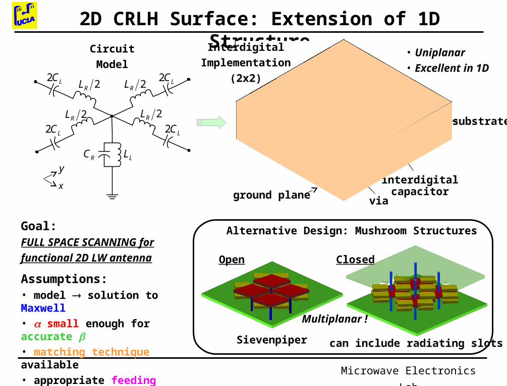
Validation of CRLH Approach and Model in 2D
Fre
quen
cy (
GH
z)
8
4
2
0X M
closed (TE)
air modeai
r m
ode
6
open (TE)
open
open (TE)
closed (TE)
closed
theory
full-wave simulation
theory
full-wave simulation
CRLH Model & Full-Wave
Dispersion Diagram for
Closed and Open Mushroom
Observations:
• Excellent agreement for TEM Maxwell ok with 2D open CRLH
• Leakage factor small enough can be neglected in model
accurate and Z0
• Accurate LW radiation predictions expected
CRLL2C Ly
2CLx
2C Ly
L Ry/2
LRx/2
LRx/22CLx
L Ry/2
x
y
y
x
#2quasi-TEM
#1 TE
Extraction Technique:
Cutoffs & Bloch Impedance

Microwave Electronics Lab
Fields Distributions in Interdigital Structure
Full Wave Dispersion Diagram Modes Distributions
3
3.5
4
4.5
5
5.5
6
6.5
7
0 0.1 0.2 0.3 0.4 0.5
2E
3E
4E
2H
3H
4H
2S
3S
4S
x
x
x
Mode2: LH, QUADI-TEM
Mode 3: RH, TE
Mode 4: RH, LH, QUADI-TEM
X3
4
5
6
7
TM
(GHz)f
RC
1
L RL C
1
R LL C

Microwave Electronics Lab
Array Factor Approach of LW Structures (1D)
Phased Array Leaky-Wave Structure
1 sin0
1
Nj n kp
n
AF I e
• linear phase:
• constant magnitude:
• excitation: feed at each element
• array factor:
0n n
0 ,nI I n
DISCRETE EFFECTIVELY HOMOGENEOUS
1 sin
1
Nj n kp
nn
AF I e
• linear phase : uniform structure
• exponentially decaying magnitude:
• excitation: induced by propagation
• array factor:
10with n p
nI I e
directivity N
x
z
p
1 1,I
2 3 40
0I 0I 0I 0I 0I
2 2,I 3 3,I 4 4,I 5 5,I
0I 01 sinn n kp
x
z
p 2 3 40
0I
0nxI e
0I
01 sinn n kp

Microwave Electronics Lab
Comparison Ckt/AF and Measured PatternsBackward, 3.5 GHz Broadside, 3.9 GHz Forward, 4.3 GHz
meas. meas. meas.
N = 25 N = 100
X
(G
Hz)
f
RH
LH

Microwave Electronics Lab
Array Factor Approach for 2D LW Structures
1 sin cos1
1
1 sin sin
11
where,
x x
y y
xm yn
Mj m kp
xm mm
Nj n kp
yn nn
AF S S
S I e
S I e
0 0
0 0
sin cos
sin sinx x
y y
kp
kp
xpx
yz
yp
M
90
xk yk
,n x yk k
0LH
RH
radiationcone
Brillouin Zone
X

Microwave Electronics Lab
3D-LH Metamaterial: TL Analysis
x
y
z
oxA
oxBo
xC oxD
iyA
iyB
iyC
iyD
oyA
oyB
oyC
oyD
ozA
ozB
ozC
ozD
izA
izB
izC
izD
ixA
ixBixCixD
0V
gA gB
gC gD
0ixI
0oxI0i
yI
0oyI
0ozI
0izI
igI
0ixV
0iyV
0oyV
0oxV
0izV
0ozV
xI
xjk axI e
yI
yjk byI e
zI
zjk czI e
xV
xjk axV e
yV
yjk byV e
zV
zjk czV e
0igV
0ogI

Microwave Electronics Lab
3D-LH Metamaterial: TL Dispersion Diagram
LH
RH
1 nH, 1 pHR L R LL L C C

Microwave Electronics Lab
3D-LH Metamaterial: Possible Unit Cell
RL
LCRC
LL
RL
RC
LC
LL

Microwave Electronics Lab
3D-LH Metamaterial: Preliminary Result
sgn sgnp gv v
LH
So far, still flat,whereas LH => negative;should be achievable be reducing series Lor increasing series C
Microwave Electronics Lab
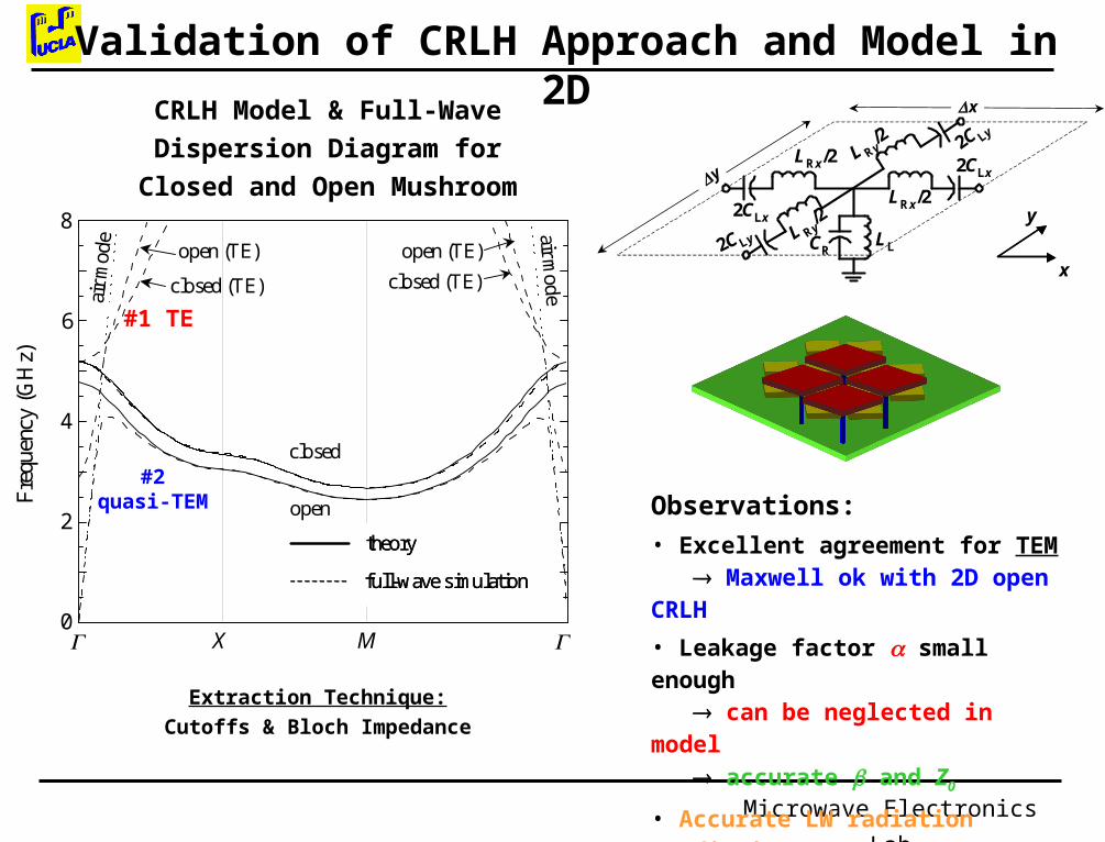
RH / LH Surface Plasmon in LC Network
0 052.8 , 7.5 , 422.5 , 60 , 2.83 ,R R L LC fF L nH C fF L nH f GHz f f
RH LH
zRk zLk
xk
xkz
x
RH LH
zRk zLk
xk
xk LR z
x
Voltage Magnitude
Voltage Phase
RH LH
RC
2RL
2RL2RL
2RL
LL
2 LC
2 LC
2 LC2 LC
zx
zRk zLk
xk
xk
RH / LH Transmission Line Interface
0 : L R L Rn n
0
RL
LH RH
R R RL C
1L
L LL C
04
1
R R L LL C L C
MICROWAVE SP Low-loss SP frequency not related to physical length

Microwave Electronics Lab
RH / LH Interface Plasmons (TM)
2
2 2 2 22
1 1
2 2 1 20
1 2
0 and 0 : 1 and 1
cste 0 and cste 0
0,
pr r
x SPk k
2xck
SP
xk
SP
lightline
loosely bound
tightly bound
p
non-radiativeSP
radiativeSP
SP gap
Rexk
Rexk
Imxk
2 20 1 1 2
2 21 0 1 1 1 2 1 22
2 2
, 0 : ,1
1=j and =j
1
1 OR 1
x r r
z r r z z
k k
k k k k
conventional SP
metal: 2 0
diel.: 1 0
x
zLH SP
LH: 22 , 0
RH: 1 1, 0
x
z
Reference: R. Ruppin, “Surface Polaritons of Left-Handed Medium”, Phys. Lett. A 277 (2000), 61-64
2 2 2 22 2
1 1
1 2 1 2 2 12 2 20 0 1 12 2 2
2 1
1 10 and 0 : and
and
,1
L L
R R
r r r r r rx r r
r r
L C
C L
k k k
2 1 2 1with ,

Microwave Electronics Lab
Dispersion Curves With Air Line and RSP
1 2 1 2 2 12 20 2 2
2 1
Dispersion relation (TM):
r r r r r rx
r r
k k
1 0 1 0
1 , 1 , 30
, , 0, 0L L
TL TL
L nH C pF a mm
C L
1 0 1 0
1 , 0.01 , 30
, , 0, 0L L
TL TL
L nH C pF a mm
C L
one SP, non radiative
,1 ,29.76 GHz 0.009 GHzSP SPf f j
1 0 1 0
1 , 0.01 , 30
, , 10 , 1L L
TL TL
L nH C pF a mm
C pF L H
,1 ,29.37 GHz 10.08 GHzSP SPf f
SP
two partly radiative SPs + 1 strange
Still Under Investigation !!!
,1 ,29.77 GHz 9.77 GHzSP SPf f j
Funny, no ?
one SP, partly radiative
branchpoint
Brewster angle
NOVELTIES:• SPs exist• -scanned Brewster angle• 2 Brewster angles possible
![A LEAKY WAVE SLOT ANTENNA ARRAY USING SIN- GLE METAL …oa.ee.tsinghua.edu.cn/~liyue/paper/2013_A Leaky Wave Slot Antenn… · have been reported in the recent literatures [8{17]](https://img.pdfslide.us/doc/110x75/5e916d0da666a0666e0d2ea1/a-leaky-wave-slot-antenna-array-using-sin-gle-metal-oaee-liyuepaper2013a-leaky.jpg)


![400GHz 1.3dBi Leaky Wave Antenna in CMOS 1.3 mProcessjpier.org/PIERC/pierc69/19.16091402.pdf · the half-wavelength dipole [4], the patch antenna [5], and the slotted cavity [7] are](https://img.pdfslide.us/doc/110x75/5e691c179ab11c0d363e66eb/400ghz-13dbi-leaky-wave-antenna-in-cmos-13-the-half-wavelength-dipole-4-the.jpg)