Embed Size (px)
Citation preview
Microscopy studies of semiconductor surfacesfor nanowire growth
Emelie HilnerDepartment of Synchrotron Radiation Research
Lund University
2008


List of papers:
My contribution to paper I includes performing the STM experiments, analy-sis of the data and writing the paper. For paper II I performed the STMexperiments, data analysis and was responsible for writing the text for theSTM part.
Paper I
Au wetting and nanoparticle stability on GaAs(111)BE. Hilner, A. Mikkelsen, J. Eriksson, J. N. Andersen, E. Lundgren, A. Za-kharov, H. Yi and P. KratzerApplied Physics Letters 89, 251912 (2006)
Paper II
Epitaxial Growth of Indium Arsenide Nanowires on Silicon Using NucleationTemplates Formed by Self-Assembled Organic CoatingsT. Martensson, J. B. Wagner, E. Hilner, A. Mikkelsen, C. Thelander, J.Stangl, J. Ohlsson, A. Gustavsson, E. Lundgren, L. Samuelson and W. SeifertAdvanced Materials 19, 1801 (2007)

Contents
1 Introduction 1
2 Nanowires 3
3 STM 73.1 Operation . . . . . . . . . . . . . . . . . . . . . . . . . . . . . 73.2 Experimental set up . . . . . . . . . . . . . . . . . . . . . . . 93.3 Theory of tunneling . . . . . . . . . . . . . . . . . . . . . . . . 9
4 LEED 134.1 Operation and experimental set up . . . . . . . . . . . . . . . 134.2 Reconstructions and adsorbate structures . . . . . . . . . . . . 14
5 SPELEEM 175.1 Experimental set up . . . . . . . . . . . . . . . . . . . . . . . 175.2 LEEM, μ-LEED and MEM . . . . . . . . . . . . . . . . . . . 185.3 PEEM and PES . . . . . . . . . . . . . . . . . . . . . . . . . . 20
6 Sample preparation 236.1 GaAs(111) . . . . . . . . . . . . . . . . . . . . . . . . . . . . . 236.2 Silicon . . . . . . . . . . . . . . . . . . . . . . . . . . . . . . . 25
7 Concluding remarks 27
8 Acknowledgements 29
i

Chapter 1
Introduction
The research presented in this thesis is mainly concerned with the propertiesof semiconductor surfaces. It is to a large part motivated by optimizationof the growth of freestanding semiconductor nanowires. Nanowires are com-monly grown by epitaxial growth methods from semiconductor substrates.The surface structure and properties of these substrates are in many casespoorly understood.
Nanowires have many promising future applications in physics, chemistryand biology of which some examples are presented in chapter one. If the fullpotential of nanowires is to be realized, extreme control of their structureand composition is essential. Such control can be achieved by a detailedunderstanding of the actual growth mechanism, which includes for exampleunderstanding the diffusion of the growth materials on the substrate surface.The surface structure of the substrate has then to be known in order tomake accurate predictions and models. Nanowire growth is often assistedby nanometer sized gold particles deposited on the substrate surface. It istherefore important to understand how gold interacts with the substrate. Ithas recently been found that it is also possible to grow nanowires without theuse of gold particles. Instead an organic coating can be used that partiallyinhibits oxidation of the substrate surface, leading to spontaneous nanowiregrowth.
Scanning Tunneling Microscopy (STM) has the ability to resolve individualatoms, making this technique essential in order to study the detailed structureof the substrates on which nanowires are grown. Spectroscopic Photo Emis-sion and Low Energy Electron Microscopy (SPELEEM) provides video ratereal space imaging with structural and chemical contrast as well as diffrac-
1
2 CHAPTER 1. INTRODUCTION
tion imaging. Combined, the two techniques provides an extremely powerfulapproach to investigating nanowire growth surfaces. The combination havebeen used in this thesis to study the interaction of gold particles with thegrowth substrate (paper I) and both techniques will be described in somedetail.
Concerning the results, in the first study, the influence of both a gold filmand gold aerosol nano particles on GaAs(111)B surface is investigated. Inboth cases, a thin gold wetting layer on the surface is found after annealingto temperatures typical of nanowire growth. By simulating the STM imagesfrom a Density Functional Theory (DFT) based model, a structure with agold atom present in every third hcp site of the Ga lattice is proposed forthe wetting layer. It is also shown that the stability of the gold particles isdirectly influenced by the presence of the surface structure.
In the second study, the STM images show that a Si(111) surface treatedwith an organic coating, displays small patches, after an anneal in Ultra HighVacuum (UHV). These patches can be related to the spontaneous growth ofnanowires, and is explained by the inhibition of oxidation of parts of the Sisubstrate when exposed to air, due to inhomogeneities in thickness of theorganic coating.
Both studies show the importance of a detailed characterization of the growthsubstrates, in order to enhance the understanding of nanowire growth. Onechapter of this thesis is also dedicated to sample preparation, since a lotof time spent on surface studies goes into finding the proper procedure ofcleaning and preparation with minimal damaging of the sample before themeasurement.
Chapter 2
Nanowires
In this thesis only epitaxially grown freestanding semiconductor nanowireswill be considered. These are rod shaped crystalline structures with diametersin the order of tens of nanometers and lengths of a few micrometers (figure2.1). The nanowires can consist of one single material, or different materialscan be combined in the same wire to realize axial and radial hetero structures.Nanowires have attracted a lot of scientific interest in the last years, mainlybecause of their many promising applications as building blocks in devicesfor e.g. electronics, optoelectronics and life sciences. A few examples ofsuch applications are new types of vertical field effect transistor structures[1], nano light emitting diodes with the ability of emitting in many differentwavelengths depending on nanowire composition [2, 3], and as tools to studythe function of nerve cells [4, 5].
One common way to synthesize nanowires is through metal, often gold, par-ticle assisted growth. Nanometer sized gold particles can be deposited byaerosol deposition [6], or a gold film is evaporated onto the substrate (fig-ure 2.2.a). Upon annealing in the growth chamber the film condenses intogold islands [7]. Nanowires are grown with different epitaxial growth tech-niques. Epitaxial means oriented growth onto a crystalline substrate. Ex-amples of techniques are molecular beam epitaxy (MBE), chemical beamepitaxy (CBE) or metalorganic vapor phase epitaxy (MOVPE). MBE is car-ried out in ultra high vacuum (UHV) where elemental growth materials areevaporated on to the substrate. UHV refers to a pressure below about 10−9
mbar. Because of the UHV conditions, the growth materials will travel tothe substrate in beams. In MOVPE the growth materials are metal-organicsand hydrides that are flowed over the substrate in a carrier gas. For thelow-pressure MOVPE system in which the wires in paper II were grown, the
3
4 CHAPTER 2. NANOWIRES
(b)
100 nm100 nm
(a)
(c)
Gold particle
Substrate
Segments
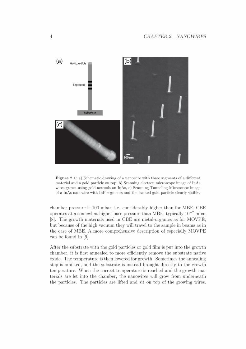
Figure 2.1: a) Schematic drawing of a nanowire with three segments of a differentmaterial and a gold particle on top, b) Scanning electron microscope image of InAswires grown using gold aerosols on InAs, c) Scanning Tunneling Microscope imageof a InAs nanowire with InP segments and the faceted gold particle clearly visible.
chamber pressure is 100 mbar, i.e. considerably higher than for MBE. CBEoperates at a somewhat higher base pressure than MBE, typically 10−7 mbar[8]. The growth materials used in CBE are metal-organics as for MOVPE,but because of the high vacuum they will travel to the sample in beams as inthe case of MBE. A more comprehensive description of especially MOVPEcan be found in [9].
After the substrate with the gold particles or gold film is put into the growthchamber, it is first annealed to more efficiently remove the substrate nativeoxide. The temperature is then lowered for growth. Sometimes the annealingstep is omitted, and the substrate is instead brought directly to the growthtemperature. When the correct temperature is reached and the growth ma-terials are let into the chamber, the nanowires will grow from underneaththe particles. The particles are lifted and sit on top of the growing wires.
5
Supply growth materials
Growth
Deposition of Au aerosol nano particles
Evaporation of gold filmon to substrate
Substrate
Spin on organic film
Anneal ingrowthchamber
Anneal ingrowthchamber
Supply growth materials
Growth
(a)
(b)
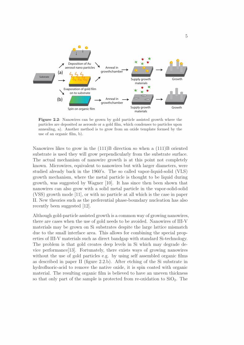
Figure 2.2: Nanowires can be grown by gold particle assisted growth where theparticles are deposited as aerosols or a gold film, which condenses to particles uponannealing, a). Another method is to grow from an oxide template formed by theuse of an organic film, b).
Nanowires likes to grow in the (111)B direction so when a (111)B orientedsubstrate is used they will grow perpendicularly from the substrate surface.The actual mechanism of nanowire growth is at this point not completelyknown. Microwires, equivalent to nanowires but with larger diameters, werestudied already back in the 1960’s. The so called vapor-liquid-solid (VLS)growth mechanism, where the metal particle is thought to be liquid duringgrowth, was suggested by Wagner [10]. It has since then been shown thatnanowires can also grow with a solid metal particle in the vapor-solid-solid(VSS) growth mode [11], or with no particle at all which is the case in paperII. New theories such as the preferential phase-boundary nucleation has alsorecently been suggested [12].
Although gold-particle assisted growth is a common way of growing nanowires,there are cases when the use of gold needs to be avoided. Nanowires of III-Vmaterials may be grown on Si substrates despite the large lattice mismatchdue to the small interface area. This allows for combining the special prop-erties of III-V materials such as direct bandgap with standard Si-technology.The problem is that gold creates deep levels in Si which may degrade de-vice performance[13]. Fortunately, there exists ways of growing nanowireswithout the use of gold particles e.g. by using self assembled organic filmsas described in paper II (figure 2.2.b). After etching of the Si substrate inhydrofluoric-acid to remove the native oxide, it is spin coated with organicmaterial. The resulting organic film is believed to have an uneven thicknessso that only part of the sample is protected from re-oxidation to SiO2. The

6 CHAPTER 2. NANOWIRES
film is evaporated when annealing the sample before growth and the resultis a mask of SiO2 that inhibits growth, and patches with SiOX from whichthe wires can nucleate and grow.
Chapter 3
STM
3.1 Operation
The scanning tunneling microscope (STM) makes use of the quantum me-chanical tunnel effect for imaging surfaces. A sharp tip of usually tungsten ora platinum-iridium alloy is brought close to a conducting sample. When thedistance between the tip and the sample is sufficiently small, their electronicwave functions will start to overlap and tunneling of electrons is possible. Ifa bias voltage is applied between the tip and the sample, a net tunneling cur-rent can be measured. In the simplest approximation the tunneling currentcan be shown to depend on the distance between the tip and the sample, d,and the height of the vacuum barrier, φ, as [14]
I ∝ e−2d√
2mφh (3.1)
The tunneling current depends exponentially on the tip sample separation,and this is what gives the excellent resolution of STM.
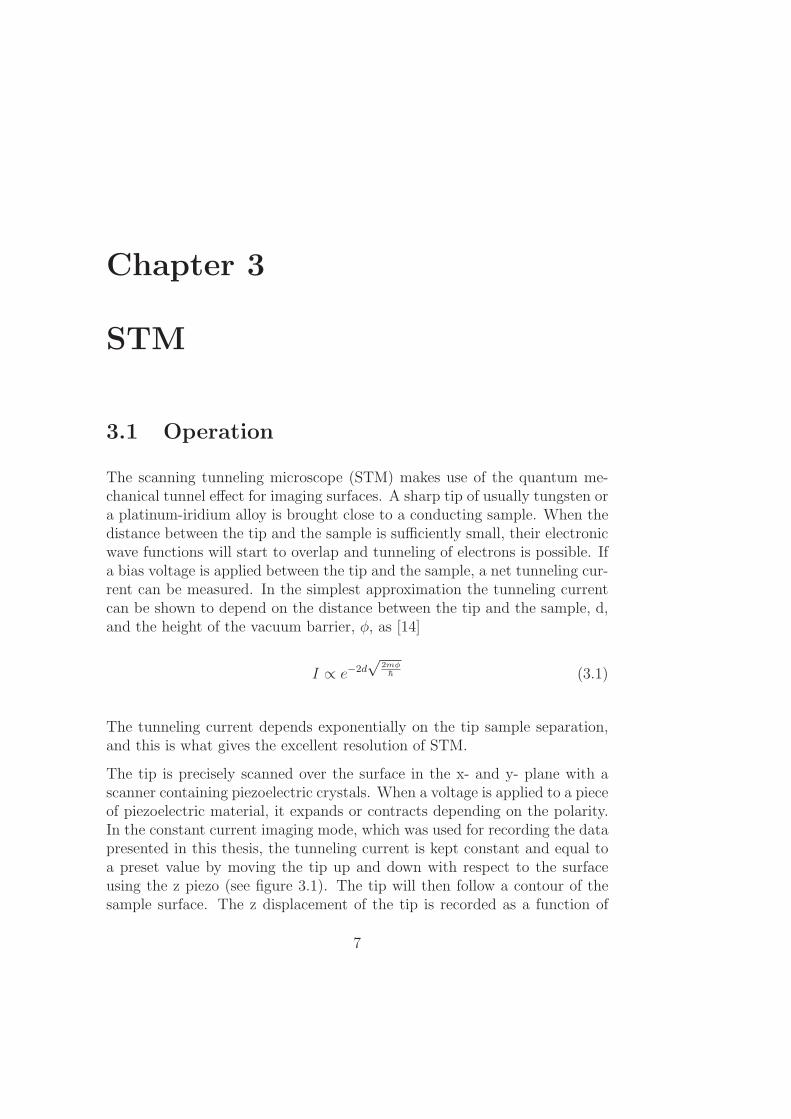
The tip is precisely scanned over the surface in the x- and y- plane with ascanner containing piezoelectric crystals. When a voltage is applied to a pieceof piezoelectric material, it expands or contracts depending on the polarity.In the constant current imaging mode, which was used for recording the datapresented in this thesis, the tunneling current is kept constant and equal toa preset value by moving the tip up and down with respect to the surfaceusing the z piezo (see figure 3.1). The tip will then follow a contour of thesample surface. The z displacement of the tip is recorded as a function of
7
8 CHAPTER 3. STM
Piezoscanner
Sample
Tip
Tip pathe-
Computer
Tunneling current
Current amplifier
ComparatorPreset value
Voltagesupply
Z
Z-value
Samplebias
X
Y
Voltagesupply
Voltagesupply
Image
Figure 3.1: Schematic drawing of the principle of operation and the control circuitof an STM operating in the constant current mode. The voltage to the z piezo andthus the tip z displacement is controlled by a feedback loop. The loop comparesthe measured tunneling current with the preset value and adjusts the tip z positionaccordingly. The movement of the tip is translated into an image by the computer.
position and translated into an image with colors or a gray scale representingthe variation in z values. It is also possible to operate the STM in theconstant height mode. The z displacement of the tip is then kept constant,and the changes in tunneling current is directly recorded and translated intoan image. The advantage of using this mode is that it is faster, but it alsorequires a very flat surface for the tip not to crash into something.
An STM measurement usually takes a couple of days, and the sample needsto be kept clean of contaminants during this time to record high qualityimages. This is only possible if the sample and the STM unit itself is kept inan environment with few gas molecules impinging and sticking to the sample
3.2. EXPERIMENTAL SET UP 9
surface per second. Therefore STM measurements needs to be carried outinside an UHV chamber if the sample is not particularly inert. An exampleof such inert material that can be imaged with STM in air is ”highly orderedpyrolytic graphite”, HOPG.
Because of the extremely small separation between the sample and tip duringthe measurement, another prerequisite for good high resolution STM imagesis effective vibrational isolation. If the STM is operated in UHV, often thevacuum system is placed on a table with some built in vibrational damping.The STM unit inside the vacuum chamber can also be further vibrationdamped. The STM’s used for obtaining the results in this thesis is dampedby spring suspension combined with magnetic damping. The STM unit iseasier to damp from vibrations than for example the Photo Emission ElectronMicroscope (PEEM) also present on the same vacuum chamber as one of theSTM’s used in this thesis. This is because only very local damping is neededfor the comparatively compact STM unit as opposed to the PEEM wherethe much larger column containing the electron optics has to be damped asa whole. Vibrations are therefore in reality much less of a problem whenperforming STM measurements compared to PEEM measurements.
3.2 Experimental set up
For the measurements presented in this thesis two different commercial Omi-cron [15] STM’s, STM1 and VT STM XA, were used. Both STM’s operateat room temperature and in a base pressure of 1 × 10⁻¹⁰ mbar.
The tips used are tungsten tips prepared by electrochemical etching [16].After inserting a tip into the UHV chamber, it is cleaned to remove theremaining oxide by sputtering with Ar+ ions and sometimes it is also flashedto a couple of hundred degrees C before being used.
3.3 Theory of tunneling
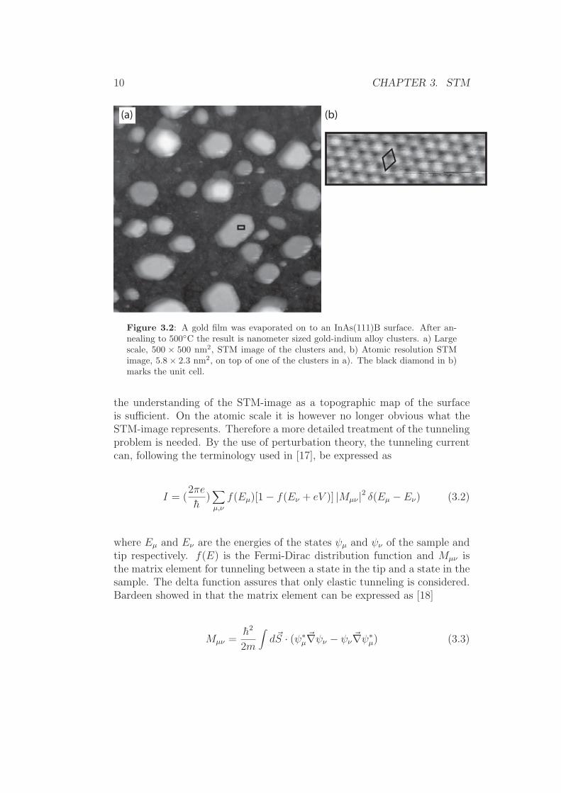
STM allows to image features on the nanometer scale as well as on theatomic scale. An example is the gold-indium alloy clusters shown in fig 3.2.When annealing a thin gold film evaporated on to a InAs substrate, the filmwill react with the substrate and condense to hexagonal gold-indium clusters(see also figure 2.2). When studying large features on the nanometer scale,
10 CHAPTER 3. STM
(a) (b)
Figure 3.2: A gold film was evaporated on to an InAs(111)B surface. After an-nealing to 500◦C the result is nanometer sized gold-indium alloy clusters. a) Largescale, 500 × 500 nm2, STM image of the clusters and, b) Atomic resolution STMimage, 5.8 × 2.3 nm2, on top of one of the clusters in a). The black diamond in b)marks the unit cell.
the understanding of the STM-image as a topographic map of the surfaceis sufficient. On the atomic scale it is however no longer obvious what theSTM-image represents. Therefore a more detailed treatment of the tunnelingproblem is needed. By the use of perturbation theory, the tunneling currentcan, following the terminology used in [17], be expressed as
I = (2πe
h)∑μ,ν
f(Eμ)[1 − f(Eν + eV )] |Mμν |2 δ(Eμ − Eν) (3.2)
where Eμ and Eν are the energies of the states ψμ and ψν of the sample andtip respectively. f(E) is the Fermi-Dirac distribution function and Mμν isthe matrix element for tunneling between a state in the tip and a state in thesample. The delta function assures that only elastic tunneling is considered.Bardeen showed in that the matrix element can be expressed as [18]
Mμν =h2
2m
∫d�S · (ψ∗
μ�∇ψν − ψν
�∇ψ∗μ) (3.3)
3.3. THEORY OF TUNNELING 11
where ψT and ψS are states in the tip and sample respectively, and the surfaceintegral should be evaluated over any surface entirely in the vacuum region.
The wave functions for the surface and the tip must be known to calculatethe matrix element. It is however very difficult to know the exact structureof the tip. In the famous calculations of Tersoff and Hamann [17], a ”perfect”tip with a spherical apex and s-like wave functions are used. With this modelthe tunneling current is shown to be proportional to the local density of states(LDOS) at the fermi level at the position, �r0 of the tip
I ∝ ∑ |ψν(�r0)|2 δ(Eν − EF ) ≡ ρ(�r0, EF ). (3.4)
In the derivation of this expression it is assumed that the tunneling voltageused is low, around 10 meV [19], which is a good approximation when imagingmetals. When imaging semiconductors, the tunneling bias voltage is oftenmuch higher. For such measurements contributions to the tunneling currentwill also come from states within an energy range of eV with respect to theFermi level. This can be expressed, using undistorted wave functions as anapproximation [14]
I ∝∫ eV
0ρsample(Ef − eV + ε) · ρtip(Ef + ε) · T (ε, eV )dε (3.5)
where T is a transmission probability.
In some cases there will be a chemical contrast in the STM image. Whenthe sample is positively biased with respect to the tip, electrons will tunnelfrom the tip to the sample and empty states of the sample are probed. Ifthe sample is negatively biased with respect to the tip, electrons will tunnelfrom the sample to the tip and filled states of the sample are probed. For theGaAs(110) surface where the filled states are located around the As atomsand the empty states around the Ga atoms, the polarity of the tunnelingcurrent therefore decides which chemical species are seen in the image.
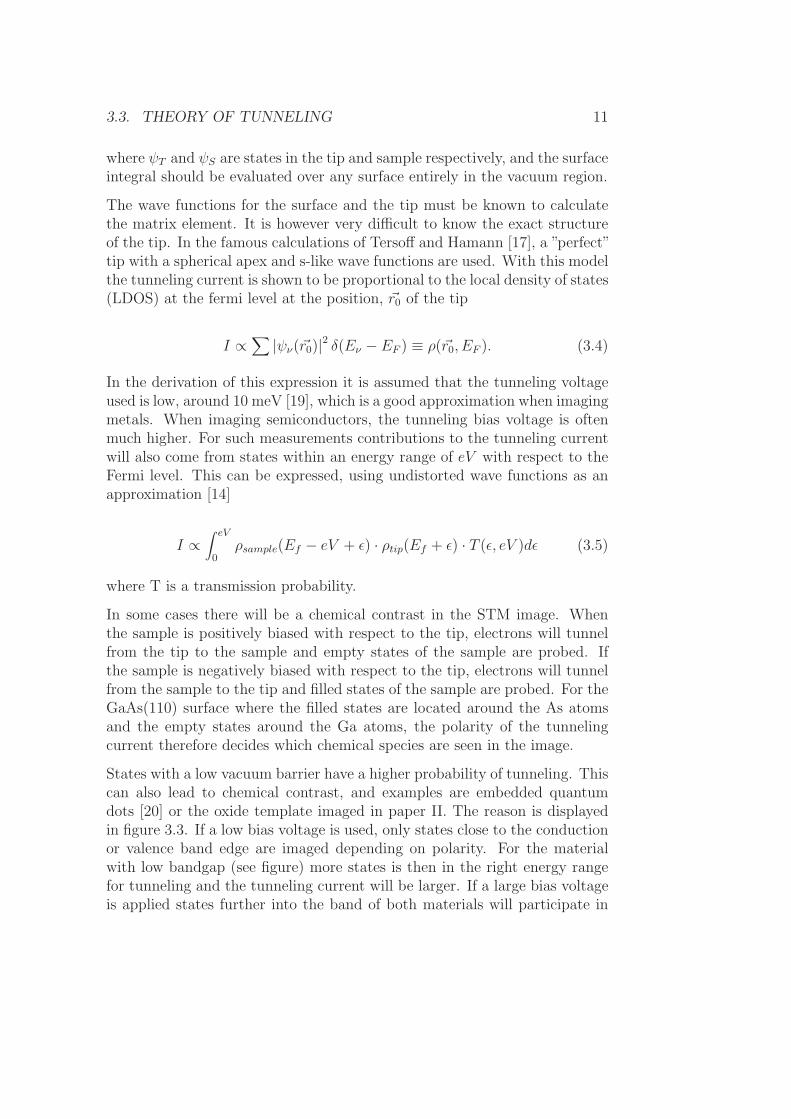
States with a low vacuum barrier have a higher probability of tunneling. Thiscan also lead to chemical contrast, and examples are embedded quantumdots [20] or the oxide template imaged in paper II. The reason is displayedin figure 3.3. If a low bias voltage is used, only states close to the conductionor valence band edge are imaged depending on polarity. For the materialwith low bandgap (see figure) more states is then in the right energy rangefor tunneling and the tunneling current will be larger. If a large bias voltageis applied states further into the band of both materials will participate in
12 CHAPTER 3. STM
Conduction band
Valence band
Large bandgapmaterial
Small bandgapmaterial
Energy
States contributing totunneling current forlow bias
States contributing totunneling current forlarge bias
x
Vacuum level
Vaccum barrier
Figure 3.3: The tunneling probability for a state depends on the vacuum barrierheight. This can give a chemical contrast in the STM image. For low bias voltagesthe band edge states are imaged and more states are in the right range of tunnelingfor the low bandgap material. At higher bias, since the states with the lowestvacuum barrier contributes most to the tunneling current, the chemical contrastwill be suppressed and there will be mostly topographical contrast. This figure issimilar to figure 1.c found in [20].
tunneling and the difference in vacuum barrier of the states close to the bandedge will play a smaller role. For the valence band, the relative differencein vacuum barrier will be smaller even for lower bias voltage. To enhancetopography contrast thus a large bias and/or filled states imaging conditionsshould be used.
Chapter 4
LEED
4.1 Operation and experimental set up
Electron gun
G3G2G1Fluorescent
screen
E
6 kV-E +Δ
Sample
Diffractedbeam
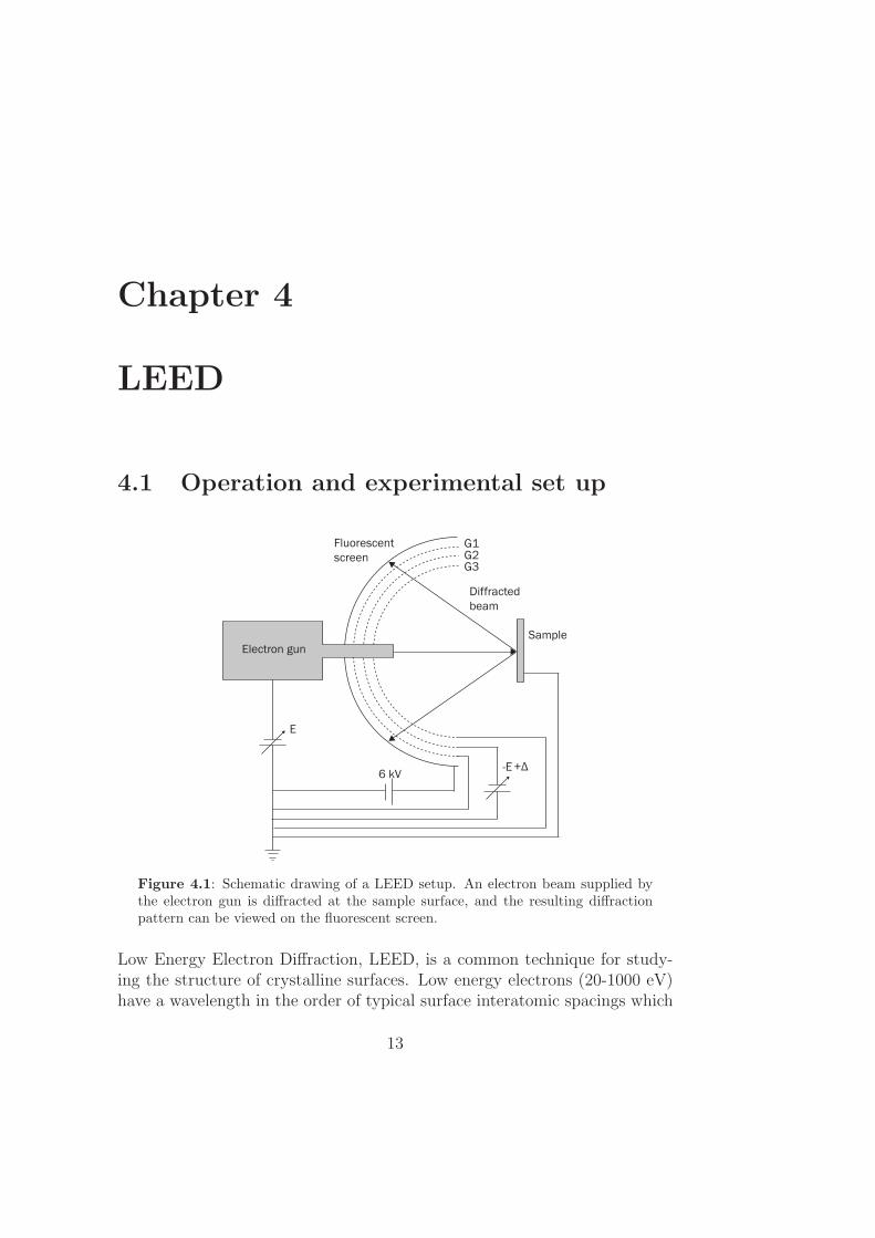
Figure 4.1: Schematic drawing of a LEED setup. An electron beam supplied bythe electron gun is diffracted at the sample surface, and the resulting diffractionpattern can be viewed on the fluorescent screen.
Low Energy Electron Diffraction, LEED, is a common technique for study-ing the structure of crystalline surfaces. Low energy electrons (20-1000 eV)have a wavelength in the order of typical surface interatomic spacings which
13
14 CHAPTER 4. LEED
enables diffraction. They also have a short penetration depth, 0.5-2 nm [21],into the sample which makes them a surface sensitive probe. In the LEEDexperiment, a beam of accelerated electrons, supplied by the electron gun,is incident normal to the sample surface. The elastically scattered electronsundergo diffraction and the result is new beams in directions according to
Δ�k‖ = |�k′‖| − | �k0‖| = ±�G (4.1)
where Δ�k‖ is the change in the component of the wave vector parallel to the
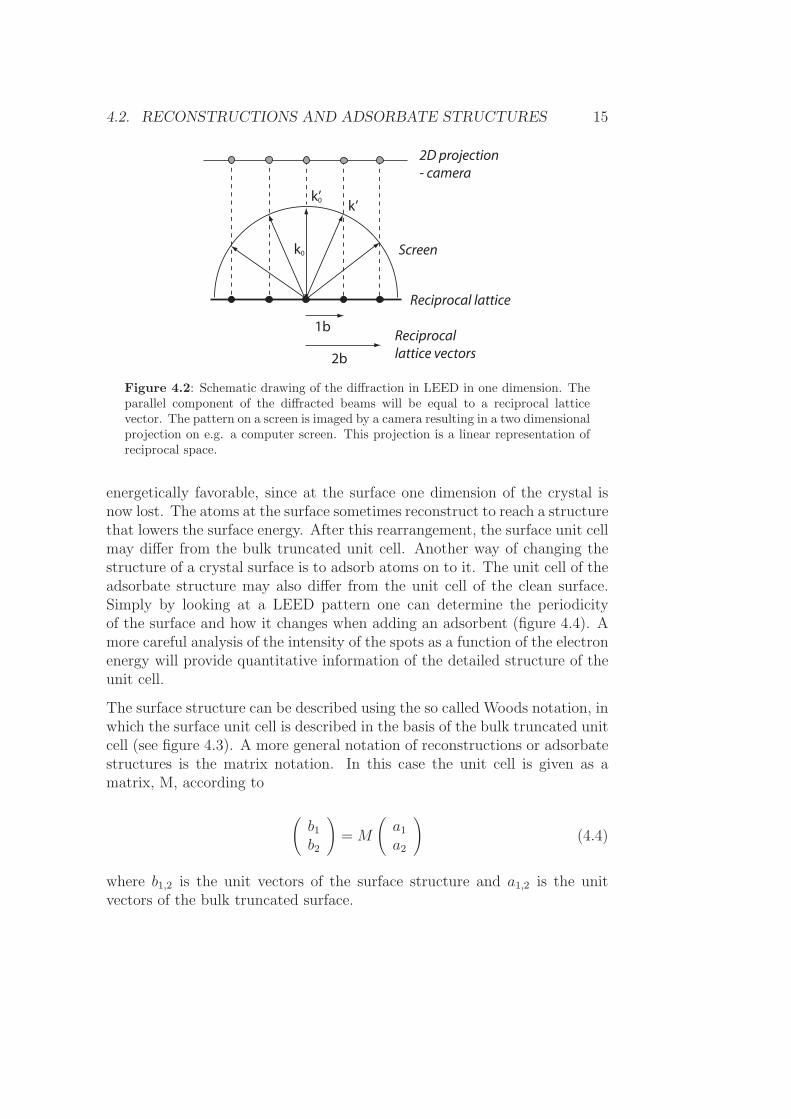
surface and �G = h�a∗+k�b∗ where h, k are integers and �a∗, �b∗ reciprocal latticevectors (see figure 4.2). The parallel component of the incoming wave vector,�k0‖, is zero since the electron beam have normal incidence. The reciprocallattice is the fourier transform of the real lattice and is defined by
|�a∗| =2π
|�a| , |�b∗| =
2π
|�b| (4.2)
�a∗ ·�b = �b∗ · �a = 0 (4.3)
where a and b are the real lattice vectors.
The resulting diffraction pattern will be displayed on the hemispherical flu-orescent screen. The screen is then usually imaged by a CCD camera andsaved onto a computer. The two-dimensional projection seen on the com-puter display is then a linear representation of the reciprocal lattice (fig.4.2). The screen only lights up when hit by electrons with sufficiently highenergy, so a high potential is applied to the screen to accelerate electronstowards it. To shield the rest of the optics from the field, a grid at groundpotential (G1) is placed in front of the screen. Grid number two (G2) is at anegative potential close to the beam energy, and reduce the background bystopping inelastically scattered electrons from reaching the screen. To avoidthat the field from G2 is interfering with the path of the scattered electrons,a third grid (G3) is placed between grid two and the sample.
4.2 Reconstructions and adsorbate structures
The surface structure of a crystal is often different from the structure inthe bulk. The bulk truncated structure of a surface is not always the most
4.2. RECONSTRUCTIONS AND ADSORBATE STRUCTURES 15
1b
2b
Reciprocal lattice
k
k’
0
k’0
Screen
Reciprocal lattice vectors
2D projection - camera
Figure 4.2: Schematic drawing of the diffraction in LEED in one dimension. Theparallel component of the diffracted beams will be equal to a reciprocal latticevector. The pattern on a screen is imaged by a camera resulting in a two dimensionalprojection on e.g. a computer screen. This projection is a linear representation ofreciprocal space.
energetically favorable, since at the surface one dimension of the crystal isnow lost. The atoms at the surface sometimes reconstruct to reach a structurethat lowers the surface energy. After this rearrangement, the surface unit cellmay differ from the bulk truncated unit cell. Another way of changing thestructure of a crystal surface is to adsorb atoms on to it. The unit cell of theadsorbate structure may also differ from the unit cell of the clean surface.Simply by looking at a LEED pattern one can determine the periodicityof the surface and how it changes when adding an adsorbent (figure 4.4). Amore careful analysis of the intensity of the spots as a function of the electronenergy will provide quantitative information of the detailed structure of theunit cell.
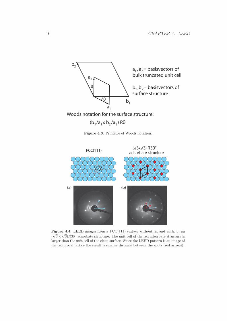
The surface structure can be described using the so called Woods notation, inwhich the surface unit cell is described in the basis of the bulk truncated unitcell (see figure 4.3). A more general notation of reconstructions or adsorbatestructures is the matrix notation. In this case the unit cell is given as amatrix, M, according to
(b1
b2
)= M
(a1
a2
)(4.4)
where b1,2 is the unit vectors of the surface structure and a1,2 is the unitvectors of the bulk truncated surface.
16 CHAPTER 4. LEED
b
b
a
a
θ
θ
a , a = basisvectors of bulk truncated unit cell
b ,b = basisvectors ofsurface structure
(b /a x b /a ) Rθ
Woods notation for the surface structure:
2
2
1
1
1 1 2 2
2
2
1
1
Figure 4.3: Principle of Woods notation.
FCC(111)(√3x√3) R30°
adsorbate structure
(a) (b)
Figure 4.4: LEED images from a FCC(111) surface without, a, and with, b, an(√
3×√3)R30◦ adsorbate structure. The unit cell of the red adsorbate structure is
larger than the unit cell of the clean surface. Since the LEED pattern is an image ofthe reciprocal lattice the result is smaller distance between the spots (red arrows).
Chapter 5
SPELEEM
SPELEEM stands for Spectroscopic Photo Emission and Low Energy Elec-tron Microscope. This microscope has several different imaging modes, en-abling video rate real space imaging, diffraction imaging as well as chemicalcontrast.
5.1 Experimental set up
In the SPELEEM system used for the experiments in this thesis, the samplecan be illuminated by low energy electrons, synchrotron light (soft x-ray) orthe light from a UV-lamp.
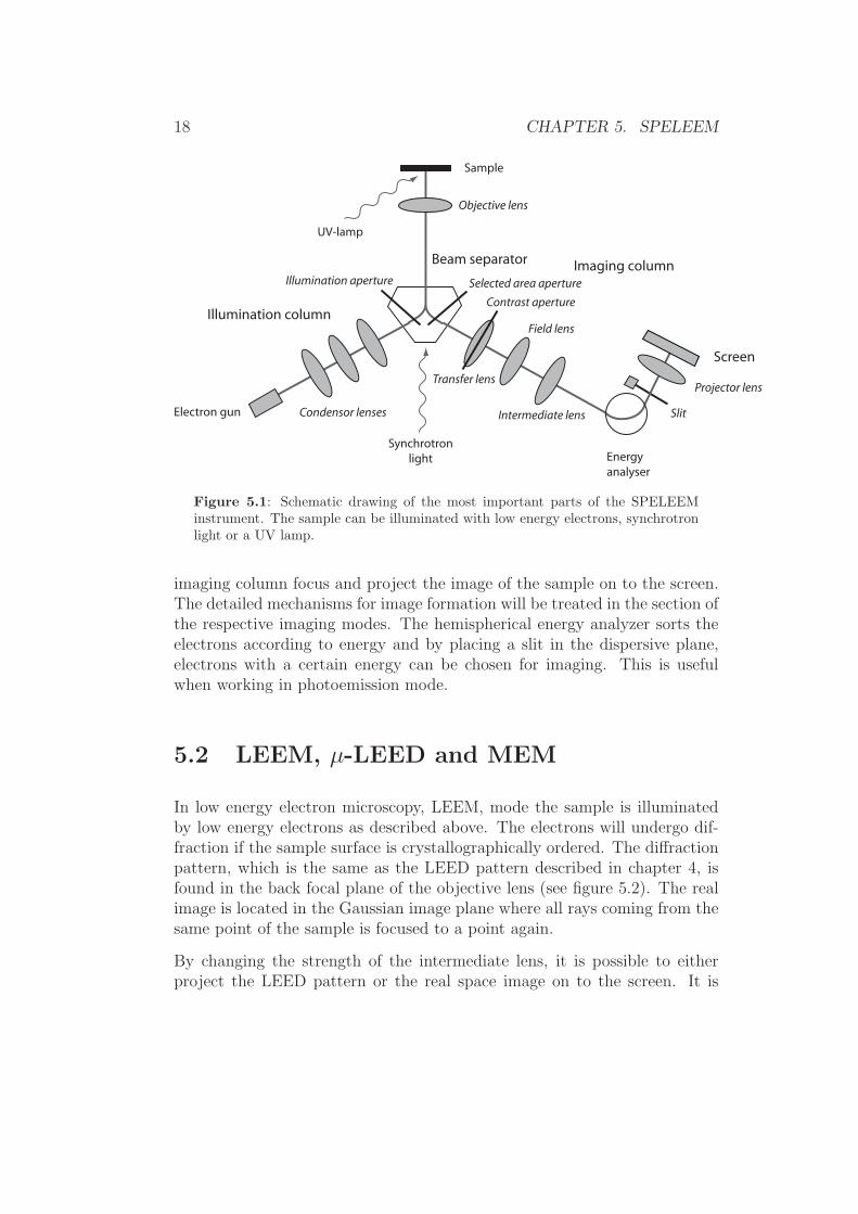
The electron illumination is supplied by a LaB6 electron gun and initially hasan energy of 20 keV. The electron beam is focused by the condenser lenses inthe illumination column. It is then deflected 60◦ by the beam separator whichseparates the incoming and outgoing beams. The objective lens is a cathodelens which means that the sample is part of the lens. The electric field inthe cathode lens is such that the electrons are decelerated to an energy ofa few electron volts on their way towards the sample, and accelerated againafter being reflected at the sample. The electrons thus travels through themicroscope at high energies except for in the objective lens. After beingreflected at the sample, the electron beam again enters the beam separatorand is deflected into the imaging column.
If the sample is instead illuminated with high energy photons in the photoe-mission mode, photo electrons are emitted. The electrons are accelerated bythe cathode lens and deflected into the imaging column. The lenses in the
17
18 CHAPTER 5. SPELEEM
Sample
Beam separator
Objective lens
Electron gun
Illumination column
Imaging column
Energyanalyser
Screen
Synchrotronlight
UV-lamp
SlitCondensor lenses
Projector lensTransfer lens
Intermediate lens
Field lens
Contrast aperture
Selected area apertureIllumination aperture
Figure 5.1: Schematic drawing of the most important parts of the SPELEEMinstrument. The sample can be illuminated with low energy electrons, synchrotronlight or a UV lamp.
imaging column focus and project the image of the sample on to the screen.The detailed mechanisms for image formation will be treated in the section ofthe respective imaging modes. The hemispherical energy analyzer sorts theelectrons according to energy and by placing a slit in the dispersive plane,electrons with a certain energy can be chosen for imaging. This is usefulwhen working in photoemission mode.
5.2 LEEM, μ-LEED and MEM
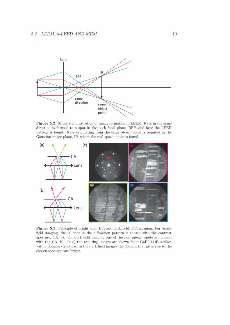
In low energy electron microscopy, LEEM, mode the sample is illuminatedby low energy electrons as described above. The electrons will undergo dif-fraction if the sample surface is crystallographically ordered. The diffractionpattern, which is the same as the LEED pattern described in chapter 4, isfound in the back focal plane of the objective lens (see figure 5.2). The realimage is located in the Gaussian image plane where all rays coming from thesame point of the sample is focused to a point again.
By changing the strength of the intermediate lens, it is possible to eitherproject the LEED pattern or the real space image on to the screen. It is
5.2. LEEM, μ-LEED AND MEM 19
BFPIP
samedirection same
objectpoint
Lens
Figure 5.2: Schematic illustration of image formation in LEEM. Rays in the samedirection is focused to a spot in the back focal plane, BFP, and here the LEEDpattern is found. Rays originating from the same object point is reunited in theGaussian image plane, IP, where the real space image is found.
BF
DF
DF
(a)
(b)
CA
CA
Lens
Lens
(c)
Figure 5.3: Principle of bright field, BF, and dark field, DF, imaging. For brightfield imaging, the 00 spot in the diffraction pattern is chosen with the contrastaperture, CA, a). For dark field imaging one of the non integer spots are chosenwith the CA, b). In c) the resulting images are shown for a GaP(111)B surfacewith a domain structure. In the dark field images the domain that gives rise to thechosen spot appears bright.
20 CHAPTER 5. SPELEEM
possible to obtain a so called μ-LEED pattern from a micrometer sized chosenspot on the sample. This is done by using either the illumination aperturelocated in the illumination column, or the selected area aperture located inthe imaging column. Aperture is basically just a fancy name for a hole in ametal plate placed in the path of the electron beam. A contrast aperture alsoneeds to be inserted in the field lens to reduce aberrations. This aperturedetermines which electrons in the diffraction pattern is used for imaging.If the electrons from the center spot of the diffraction pattern is used, theimaging mode is called bright field imaging, and if one of the non integerspots is used, it is called dark field imaging.
When using the bright field imaging mode, contrast is due to differences inintensity of the center spot of the diffraction pattern at different areas ofthe sample. If a surface has domains of the same structure (as is the casefor GaP(111)B in figure 5.3) there might be no difference in intensity of thecenter spot for the different domains. Then it is necessary to instead usedark field imaging. The domains giving rise to the diffraction spot used willappear bright in the image whereas areas belonging to a different domain willappear dark. This gives the opportunity to map out the different domainson the sample.
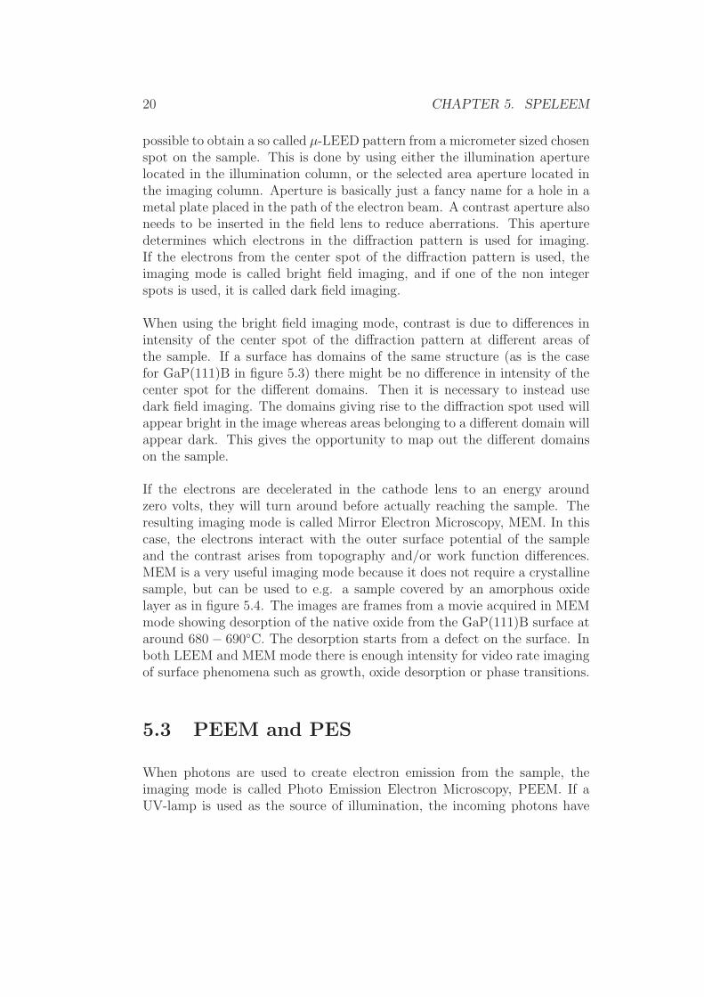
If the electrons are decelerated in the cathode lens to an energy aroundzero volts, they will turn around before actually reaching the sample. Theresulting imaging mode is called Mirror Electron Microscopy, MEM. In thiscase, the electrons interact with the outer surface potential of the sampleand the contrast arises from topography and/or work function differences.MEM is a very useful imaging mode because it does not require a crystallinesample, but can be used to e.g. a sample covered by an amorphous oxidelayer as in figure 5.4. The images are frames from a movie acquired in MEMmode showing desorption of the native oxide from the GaP(111)B surface ataround 680 − 690◦C. The desorption starts from a defect on the surface. Inboth LEEM and MEM mode there is enough intensity for video rate imagingof surface phenomena such as growth, oxide desorption or phase transitions.
5.3 PEEM and PES
When photons are used to create electron emission from the sample, theimaging mode is called Photo Emission Electron Microscopy, PEEM. If aUV-lamp is used as the source of illumination, the incoming photons have
5.3. PEEM AND PES 21
(a) T=689°C (b) T=689°C
(c) T=686°C (d) T=606°C
Figure 5.4: Four frames from a movie acquired in MEM mode showing the des-orption of native oxide from the GaP(111)B surface at 680−690◦C. The desorptionstarts from a defect on the surface. When the temperature is lowered, d, the des-orption stops.
22 CHAPTER 5. SPELEEM
Binding Energy (eV)16 18 20 22
Inte
nsity
(au)
GaP(111)B surface Droplet (x0.5)
hν = 80eV
Figure 5.5: When the GaP(111)B surface is annealed at sufficiently high tempera-ture Ga droplets form due to preferential evaporation of phosphorous. Ga 3d μ-XPSspectrum from one such droplet, and from the surrounding GaP surface respectively.
energies around 5 eV. This means that only the electrons in the highestenergy levels can be emitted. Work function differences is therefore the maincontrast mechanism.
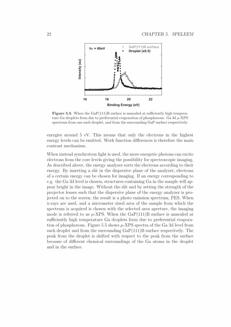
When instead synchrotron light is used, the more energetic photons can exciteelectrons from the core levels giving the possibility for spectroscopic imaging.As described above, the energy analyzer sorts the electrons according to theirenergy. By inserting a slit in the dispersive plane of the analyzer, electronsof a certain energy can be chosen for imaging. If an energy corresponding toe.g. the Ga 3d level is chosen, structures containing Ga in the sample will ap-pear bright in the image. Without the slit and by setting the strength of theprojector lenses such that the dispersive plane of the energy analyzer is pro-jected on to the screen, the result is a photo emission spectrum, PES. Whenx-rays are used, and a micrometer sized area of the sample from which thespectrum is acquired is chosen with the selected area aperture, the imagingmode is referred to as μ-XPS. When the GaP(111)B surface is annealed atsufficiently high temperature Ga droplets form due to preferential evapora-tion of phosphorous. Figure 5.5 shows μ-XPS spectra of the Ga 3d level fromsuch droplet and from the surrounding GaP(111)B surface respectively. Thepeak from the droplet is shifted with respect to the peak from the surfacebecause of different chemical surroundings of the Ga atoms in the dropletand in the surface.
Chapter 6
Sample preparation
6.1 GaAs(111)
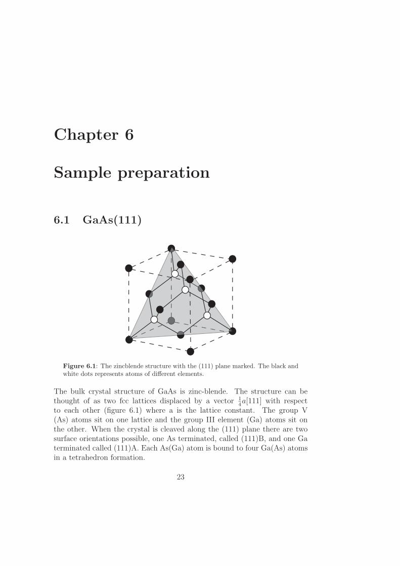
Figure 6.1: The zincblende structure with the (111) plane marked. The black andwhite dots represents atoms of different elements.
The bulk crystal structure of GaAs is zinc-blende. The structure can bethought of as two fcc lattices displaced by a vector 1
4a[111] with respect
to each other (figure 6.1) where a is the lattice constant. The group V(As) atoms sit on one lattice and the group III element (Ga) atoms sit onthe other. When the crystal is cleaved along the (111) plane there are twosurface orientations possible, one As terminated, called (111)B, and one Gaterminated called (111)A. Each As(Ga) atom is bound to four Ga(As) atomsin a tetrahedron formation.
23
24 CHAPTER 6. SAMPLE PREPARATION
As was already discussed in section 4.2, the bulk terminated structure of asurface is often not the most energetically favorable. To lower the energythe surface atoms therefore will undergo reconstruction. Many of the III-Vsemiconductor surface show different reconstructions depending on at whichtemperature they have been annealed. One reason for this is the preferentialevaporation of one of the two components of the material. When annealingat sufficiently high temperature, this also leads to the formation of metallicclusters or droplets on the surface.
On the clean GaAs(111)A a (2 × 2) reconstruction is found. Under As richconditions, a As-trimer structure has been suggested [22]. At As poor con-ditions, the reconstruction is still a (2× 2), but is instead due to a structurewhere every fourth Ga atom is replaced by a vacancy. The GaAs(111)B sur-face also exhibit a (2 × 2) As trimer structure at low temperature and Asrich conditions [23, 24, 25]. When annealing to higher temperatures, As willevaporate from the surface and a more Ga rich (
√19 ×√
19) reconstruction[26] will appear. A transitional phase called the (1 × 1)LT reconstructionexists in between the (2 × 2) and (
√19 ×√
19) reconstructions consisting ofa mixture of the two [27, 28]. Also other reconstructions such as a (3 × 3)reconstruction have been suggested [29] for the transitional phase. Whichreconstruction is found depends very much on the exact surface preparation.Sometimes different experiments are therefore difficult to compare, becausefor example the surface have been sputtered or a certain chemical prepara-tion have been used. After annealing at even higher temperature the so called(1× 1)HT reconstruction is found [27] as for the clean surface in paper I. Nodetailed structure have been proposed for this reconstruction. For high Asflux conditions, the (
√19×√
19) structure is not observed but, the (1×1)LT
and (1 × 1)HT becomes the same phase [30].
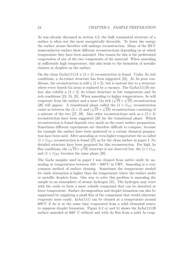
The GaAs samples used in paper I was cleaned from native oxide by an-nealing at temperatures between 450 − 600◦C in UHV. Annealing is a verycommon method of surface cleaning. Sometimes the temperature neededfor oxide desorption is higher than the temperature where the surface meltsor metallic droplets form. One way to solve this problem is annealing thesample in an atmosphere of atomic hydrogen [31]. The hydrogen may reactwith the oxide to form a more volatile compound that can be desorbed atlower temperature. Surface decomposition and droplet formation can also besuppressed by supplying a small flux of the component that would otherwiseevaporate more easily. InAs(111) can be cleaned at a temperature around600◦C if As is at the same time evaporated from a solid elemental sourceto suppress droplet formation. Figure 6.2 a) and b) shows the InAs(111)Bsurface annealed at 600◦ C without and with As flux from a solid As evap-
6.2. SILICON 25
oration source respectively. In figure 6.2.a large In droplets are seen to bepresent on the whole surface, whereas this is not the case in figure 6.2.b.
(a)
1028
(b)
ru09_210418
Figure 6.2: (190×190) nm2 STM images of the InAs(111)B surface after annealingto 600◦C. a) Without As pressure large In droplets are formed on the surface.(U = −2.5V ) b) With an As flux supplied by a solid evaporation source dropletformation is avoided. (U = −1.8V )
6.2 Silicon
The Si substrates in paper II were cleaned of oxide by etching in hydrofluoricacid (HF). The surface is after such etching procedure ideally thought to behydrogen terminated and stable with respect to further oxidation. In realityhowever, which is essential for the process in paper II to work, the surfaceslowly re- oxidizes when exposed to air. The resulting surface structure andstability after etching depends very much on the exact etching solution, andthe procedure used as is reflected in the number of publications on this subject(for example [32], [33], [34], [35] and references therein). Si can also be cleanedby annealing to temperatures higher than 1000◦C in UHV [14].

26 CHAPTER 6. SAMPLE PREPARATION
Chapter 7
Concluding remarks
The results presented in this thesis show that STM and SPELEEM is a power-ful combination for conducting surface studies. Combined these experimentaltechniques provide information about morphology, structure, chemistry anddynamics from the micrometer to the atomic scale. One example of a processthat would have been hard to understand without the combination of STMand SPELEEM is the Ga droplet mediated surface ordering of GaP(111)B.
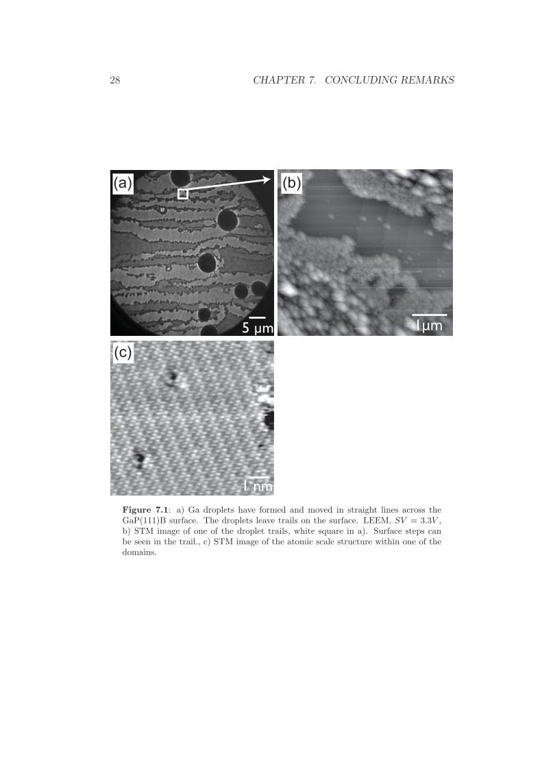
When annealing the GaP(111)B surface in front of the SPELEEM, the des-orption the native oxide can be followed in MEM mode (figure 5.4). Aftercomplete desorption of the oxide, a structure with tiny six-fold domains, tensof nano meters across, appear. Further annealing leads to the formation ofdroplets that by μ-XPS measurement (figure 5.5) can be shown to consistof mostly pure Ga. The droplets move across the surface in straight linesperpendicular and up hill to the surface steps as was concluded by STMmeasurement (figure 7.1). The droplets leave a trail as they move across thesurface. STM as well as dark field LEEM measurements show that in thetrail large micrometer sized domains of the six-fold structure is found. Theatomic scale structure within the large domains is the same as for the smalldomains. The droplets thus order small domains into larger ones as theymove across the surface.
By the use of STM only, the surface ordering would have been extremelydifficult to relate to moving Ga droplets. Similarly, detailed informationabout atomic scale arrangement would have been difficult to obtain usingSPELEEM only. Thus a full understanding was reached only by combiningSTM and SPELEEM. Other systems, for which mesoscopic properties affectthe atomic scale structure, could be studied in a similar way.
27
28 CHAPTER 7. CONCLUDING REMARKS
1μm5 μm
1 nm
(a) (b)
(c)
Figure 7.1: a) Ga droplets have formed and moved in straight lines across theGaP(111)B surface. The droplets leave trails on the surface. LEEM, SV = 3.3V ,b) STM image of one of the droplet trails, white square in a). Surface steps canbe seen in the trail., c) STM image of the atomic scale structure within one of thedomains.
Chapter 8
Acknowledgements
I would like to thank my supervisors Anders Mikkelsen and Edvin Lund-gren for all your help and support, Alexei Zakharov for teaching me aboutSPELEEM, colleagues and friends at Synchrotron Radiation Research, MAXLABand within the Nanometer Structure Consortium at Lund University. A spe-cial thanks to the aerosol group of the Division of Solid State Physics thathas supplied me with gold aerosol nano particles.
29

30 CHAPTER 8. ACKNOWLEDGEMENTS
Bibliography
[1] T. Bryllert, L-E. Wernersson, L. E. Froberg, and L. Samuelson, IEEEElectron Device Lett. 27, 323 (2006).
[2] Y. Huang, X. Duan, and C. M. Lieber, Small 1, 142 (2005).
[3] F. Qian et al., Nano Letters 5, 2287 (2005).
[4] W. Hallstrom et al., Nano Lett. 7, 2960 (2007).
[5] F. Patolsky et al., Science 313, 1100 (2006).
[6] M. H. Magnusson et al., J. Nanopart. Res. 1, 243 (1999).
[7] M. C. Plante and R. R. LaPierre, J. Cryst. Growth 310, 356 (2008).
[8] A. Persson, Ph.D. thesis, Lund University, 2005.
[9] G. Stringfellow, Organometallic vapor phase epitaxy: Theory and prac-tice, 2nd edition (Academic press, London, San Diego, 1999).
[10] R. Wagner, in Whisker Technology, edited by A. P. Levitt (Wiley-Interscience, New York, 1970), Chap. VLS Mechanism of CrystalGrowth, pp. 47–120.
[11] K. A. Dick et al., Nano Letters 5, 761 (2005).
[12] B. A. Wacaser, Ph.D. thesis, Lund University, 2007.
[13] M. Kleverman et al., Solid State Commun. 93, 383 (1995).
[14] R. Wiesendanger, Scanning Probe Microscopy and Spectroscopy - Meth-ods and Applications (Cambridge University Press, Cambridge, 2001).
[15] Omicron GmbH, http://www.omicron.de.
[16] I. Ekvall et al., Meas. Sci. Technol. 10, 11 (1999).
[17] J. Tersoff and D. R. Hamann, Phys. Rev. B 31, 805 (1985).
31
32 BIBLIOGRAPHY
[18] J. Bardeen, Phys. Rev. Lett. 6, 57 (1961).
[19] J. Tersoff and D. R. Hamann, Phys. Rev. Lett. 50, 1998 (1983).
[20] D. M. Bruls et al., Appl. Surf. Sci. 190, 258 (2002).
[21] G. Attard and C. Barnes, Surfaces (Oxford university press, Oxford,1998).
[22] J. M. C. Thornton, P. Weightman, D.A. Woolf, and C. J. Dunscombe,Phys. Rev. B 51, 14459 (1995).
[23] D. K. Biegelsen, R. D. Bringans, J. E. Northrup, and L. E. Swartz, Phys.Rev. Lett. 65, 452 (1990).
[24] A. Ohtake et al., Phys. Rev. B 64, 045318 (2001).
[25] K. W. Haberern and M. D. Pashley, Phys. Rev. B 41, 3226 (1990).
[26] H. H. Farell et al., J. Vac. Sci. Technol., B 19, 1597 (2001).
[27] J. M. C. Thornton, D. A. Woolf, and P. Weightman, Appl. Surf. Sci.123/124, 115 (1998).
[28] A. R. Avery, E. S. Tok, and T. S. Jones, Surf. Sci. 376, L397 (1997).
[29] O. E. Tereshchenko, V. L.. Alperovich, and A. S. Terekhov, Surf. Sci.600, 577 (2006).
[30] D. A Wolf, D. I. Westwood, and R. H. Williams, Appl. Phys. Lett. 62,1370 (1993).
[31] G. R. Bell, N. S. Kaijaks, R. J. Dixon, and C. F. McConville, Surf. Sci.401, 125 (1998).
[32] D. D. M. Wayner and R. A. Wolkow, J. Chem. Soc, Perkin Trans. 2, 23(2002).
[33] T-. A Miura, M. Niwano, D. Shoji, and N. Miyamoto, J. Appl. Phys.79, 4373 (1996).
[34] H. Angermann, W. Henrion, M. Reiben, and A. Roseler, Appl. Surf. Sci.235, 322 (2004).
[35] D. B. Fenner, D. K. Biegelsen, and R. D. Bringans, J. Appl. Phys. 66,419 (1989).


![High resolution scanning gate microscopy measurements on ... · Such interfaces are of relevance for a broad range of studies from high performance nanowire transistors[13][14] to](https://img.pdfslide.us/doc/110x75/5f701fc290829d35b2598ce9/high-resolution-scanning-gate-microscopy-measurements-on-such-interfaces-are.jpg)