Embed Size (px)
Citation preview

Louisiana State UniversityLSU Digital Commons
LSU Doctoral Dissertations Graduate School
2016
Microscopic Study of Structure, ChemicalComposition and Local Conductivity of La2/3Sr1/3MnO3 FilmsLina ChenLouisiana State University and Agricultural and Mechanical College
Follow this and additional works at: https://digitalcommons.lsu.edu/gradschool_dissertations
Part of the Physical Sciences and Mathematics Commons
This Dissertation is brought to you for free and open access by the Graduate School at LSU Digital Commons. It has been accepted for inclusion inLSU Doctoral Dissertations by an authorized graduate school editor of LSU Digital Commons. For more information, please [email protected].
Recommended CitationChen, Lina, "Microscopic Study of Structure, Chemical Composition and Local Conductivity of La2/3Sr1/3MnO3 Films" (2016).LSU Doctoral Dissertations. 358.https://digitalcommons.lsu.edu/gradschool_dissertations/358

MICROSCOPIC STUDY OF STURCTURE, CHEMICAL COMPOSITION AND
LOCAL CONDUCTIVITY OF La2/3Sr1/3MnO3 FILMS
A Dissertation
Submitted to the Graduate Faculty of theLouisiana State University and
Agricultural and Mechanical Collegein partial fulfillment of the
requirements for the degree ofDoctor of Philosophy
in
The Department of Physics and Astronomy
byLina Chen
B.S., Anhui University,China, 2006M.S., University of Science and Technology of China, 2009
August 2016

Acknowledgments
First I wish to express my gratitude to my supervisors, Professor Jiandi Zhang
and Ward Plummer, for supporting me during these past seven years. They have
supported me not only financially through a research assistantship, but also aca-
demically and emotionally along the tumultuous path to finishing this thesis work.
Without their help, I could not have completed my Ph.D, and this dissertation
would not be possible. Jiandi is an instantly endearing and unforgettable per-
son, and I have greatly benefited from his detailed guidance and scientific insight
throughout my Ph.D study. I sincerely appreciate his instruction and help in fin-
ishing this research. With a keen eye, Ward has always provided invaluable insight
into my research. He helped form the course of my research, and was always willing
to read through my work. His extraordinary passion for research, great knowledge,
and resourcefulness have been inspirations to me. I also would like to thank my
committee members, Dr. Rongying Jin, Dr. Juana Moreno, and Dr. Jianwei Wang
for their helpful advice and suggestions throughout my work.
It is a pleasure to thank some of the previous members of Dr. Zhang and Dr.
Plummer’s groups: Dr. Jinsun Shin, Dr. Xiaobo He, and Dr. Zhaoliang Liao. With
their help, I learned the basics of this field, as well as how to manipulate our
equipment in the ultrahigh vacuum and pulsed laser deposition systems. I also
want to thank all the present members of the Dr. Zhang, Dr. Plummer, and Dr.
Jin groups: Dr. Zhen Wang, Dr. Jisun Kim, Gaomin Wang, Dr. Hangwen Guo,
Mohammad Saghayezhian, David Howe, Dr. Chen Chen, Dr. Fangyang Liu, Zhenyu
Diao, Jianyu Pan, and Silu Huang for their collaboration and creation of a pleasant
working environment.
ii

I have found great joy these past seven years not only in the lab but also in
my life, and I owe that to my loving husband. As a Ph.D candidate, often times
experiments are unsuccessful and do not go as planned, which can be frustrating.
Ronghua was always there to give suggestions and cheered me up. He was always
right there when I needed him, and I deeply thank him.
My final and most heartfelt acknowledgement goes to my parents. Although they
cannot read or speak English, I still want to thank them here. My parents are both
traditional Chinese parents, who give their endless love, support, and care to their
children, but are also unique in many ways, and they gave me the freedom to let
me be myself. For both of these aspects, I thank them.
iii

Table of Contents
Acknowledgments . . . . . . . . . . . . . . . . . . . . . . . . . . . . . . . . . . . . . . . . . . . . . . . . . . . . . . . . . . . ii
List of Tables . . . . . . . . . . . . . . . . . . . . . . . . . . . . . . . . . . . . . . . . . . . . . . . . . . . . . . . . . . . . . . . vi
List of Figures . . . . . . . . . . . . . . . . . . . . . . . . . . . . . . . . . . . . . . . . . . . . . . . . . . . . . . . . . . . . . . vii
Abstract . . . . . . . . . . . . . . . . . . . . . . . . . . . . . . . . . . . . . . . . . . . . . . . . . . . . . . . . . . . . . . . . . . . . xiii
Chapter 1: Structure and Physical Properties of Manganites in Bulk and ThinFilm . . . . . . . . . . . . . . . . . . . . . . . . . . . . . . . . . . . . . . . . . . . . . . . . . . . . . . . . . . . . . . . . . . . . 11.1 Introduction . . . . . . . . . . . . . . . . . . . . . . . . . . . . . . . 11.2 Perovskite Structure of Manganites . . . . . . . . . . . . . . . . . . 41.3 Physical Properties of Manganites . . . . . . . . . . . . . . . . . . . 8
1.3.1 Phase Diagram of Manganites in Bulk . . . . . . . . . . . . 81.3.2 Physical Properties of Manganites Thin Films . . . . . . . . 121.3.3 Dead-layer in LSMO Thin Films . . . . . . . . . . . . . . . . 141.3.4 Surface Termination of LSMO Thin Films . . . . . . . . . . 191.3.5 Polarity Discontinuity at Interface . . . . . . . . . . . . . . . 20
1.4 Summary . . . . . . . . . . . . . . . . . . . . . . . . . . . . . . . . 22
Chapter 2: Experimental Methods . . . . . . . . . . . . . . . . . . . . . . . . . . . . . . . . . . . . . . . . . 242.1 Introduction . . . . . . . . . . . . . . . . . . . . . . . . . . . . . . . 242.2 Film growth . . . . . . . . . . . . . . . . . . . . . . . . . . . . . . . 25
2.2.1 Laser Molecular Beam Epitaxy (Laser-MBE) . . . . . . . . . 252.2.2 Reflection High Energy Electron Diffraction (RHEED) . . . 27
2.3 In− Situ Characterization . . . . . . . . . . . . . . . . . . . . . . . 292.3.1 Low Energy Electron Diffraction (LEED) . . . . . . . . . . . 302.3.2 Angle resolved X-ray Photoelectron Spectroscopy (ARXPS) 332.3.3 Scanning Tunneling Microscopy/Spectroscopy (STM/STS) . 38
2.4 Ex-situ Characterization . . . . . . . . . . . . . . . . . . . . . . . . 422.4.1 Scanning Transmission Electron Microscopy/Electron Ener-
gy Loss Spectroscopy (STEM/EELS) . . . . . . . . . . . . . 422.4.2 Physical Property Measurement System (PPMS) . . . . . . 452.4.3 Summary . . . . . . . . . . . . . . . . . . . . . . . . . . . . 46
Chapter 3: Substrate treatment and LSMO film growth . . . . . . . . . . . . . . . . . . . . 473.1 Introduction and motivation . . . . . . . . . . . . . . . . . . . . . . 473.2 The treatment of SrTiO3 substrate . . . . . . . . . . . . . . . . . . 483.3 High quality LSMO film growth . . . . . . . . . . . . . . . . . . . . 54
3.3.1 LSMO film growth . . . . . . . . . . . . . . . . . . . . . . . 543.3.2 LSMO film quality characterization . . . . . . . . . . . . . . 59
iv

3.4 Summary . . . . . . . . . . . . . . . . . . . . . . . . . . . . . . . . 61
Chapter 4: Layer-by-layer composition . . . . . . . . . . . . . . . . . . . . . . . . . . . . . . . . . . . . . 634.1 Introduction and motivation . . . . . . . . . . . . . . . . . . . . . . 634.2 LSMO film interface composition from TEM . . . . . . . . . . . . . 654.3 LSMO film surface composition from ARXPS . . . . . . . . . . . . 734.4 Summary . . . . . . . . . . . . . . . . . . . . . . . . . . . . . . . . 81
Chapter 5: Surface investigation . . . . . . . . . . . . . . . . . . . . . . . . . . . . . . . . . . . . . . . . . . . 835.1 Introduction and motivation . . . . . . . . . . . . . . . . . . . . . . 835.2 Surface morphology and local tunneling conductivity(STS/STM) . . 845.3 Layer-by-layer structure . . . . . . . . . . . . . . . . . . . . . . . . 975.4 Film properties interpretation . . . . . . . . . . . . . . . . . . . . . 1025.5 Summary . . . . . . . . . . . . . . . . . . . . . . . . . . . . . . . . 104
Chapter 6: Introduce to the segregation theory and experiment discussion inLSMO . . . . . . . . . . . . . . . . . . . . . . . . . . . . . . . . . . . . . . . . . . . . . . . . . . . . . . . . . . . . . . . . . . 1066.1 Introduction and motivation . . . . . . . . . . . . . . . . . . . . . . 1066.2 Segregation in Metal alloys . . . . . . . . . . . . . . . . . . . . . . 111
6.2.1 Experimental Methods for Study of Grain Boundary Segre-gation . . . . . . . . . . . . . . . . . . . . . . . . . . . . . . 111
6.2.2 Theoretical Study of Grain Boundary Segregation . . . . . . 1126.3 Present Results and Discussion for LSMO film . . . . . . . . . . . . 117
6.3.1 Segregation driving forces in LSMO films . . . . . . . . . . . 1186.3.2 Surface segregation in LSMO films . . . . . . . . . . . . . . 121
6.4 Summary . . . . . . . . . . . . . . . . . . . . . . . . . . . . . . . . 122
References . . . . . . . . . . . . . . . . . . . . . . . . . . . . . . . . . . . . . . . . . . . . . . . . . . . . . . . . . . . . . . . . . . 124
Vita . . . . . . . . . . . . . . . . . . . . . . . . . . . . . . . . . . . . . . . . . . . . . . . . . . . . . . . . . . . . . . . . . . . . . . . . 136
v

List of Tables
3.1 Parameters to calculate the IMFP of characteristic curves for STO . 50
3.2 List of parameters of Sr 3p, Sr 3d, Ti 2p and O 1s core levels forSTO ARXPS calculation. . . . . . . . . . . . . . . . . . . . . . . . 50
4.1 Fitting results for Sr profiles near the interface of LSMO films . . . 72
4.2 Parameters to calculate the IMFP of characteristic curves for LSMO 75
4.3 List of parameters for LSMO ARXPS Sr3d/La4d fitting. . . . . . . 75
4.4 List of parameters of Sr 3d, La 4d, Mn 2p and O 1s core levels forLSMO ARXPS calculation. . . . . . . . . . . . . . . . . . . . . . . 76
5.1 Relative atomic positions of the refined surface structure of 2 u.c.LSMO film grown on STO. . . . . . . . . . . . . . . . . . . . . . . . 99
5.2 Relative atomic positions of the refined surface structure of 6 u.c.and 10 u.c. LSMO films. . . . . . . . . . . . . . . . . . . . . . . . . 100
vi

List of Figures
1.1 Schematic diagram showing transition metal oxides with emergentphenomena due to the strong interactions among multiple degreesof freedom of correlated electron interaction. . . . . . . . . . . . . . 2
1.2 (a) The perovskite structure of manganites; (b) Field splitting of thefive-fold degenerate Mn3+ with d4 3d levels into lower t2g and highereg levels, and further splitting of t2g and eg levels due to Jahn-Teller(JT) distortion. (c) The shapes of these 3d orbitals. . . . . . . . . . 5
1.3 The electronic phase diagram of RE1−xAExMnO3 (x=0.45) bulkcrystals in the plane of < rA > and variance. FM, CO/OO AFI, andSGI represent the phases of ferromagnetic metal, charge/orbital-ordered antiferromagnetic insulator, and spin glass-like insulator,respectively. Adopted from [25]. . . . . . . . . . . . . . . . . . . . . 7
1.4 Phase diagram of RE1−xAExMnO3 systems with doping concentra-tion x and temperature T for representative distorted perovskites(a) La1−xSrxMnO3 (b) Nd1−xSrxMnO3 (NSMO) (c) La1−xCaxMnO3
(LCMO) (d) Pr1−xCaxMnO3 (PCMO). There are several electron-ic and magnetic states: paramagnetic insulating (PI); paramagneticmetallic (PM); spin-canted insulating (SCI); charge-ordered insulat-ing (COI); antiferromagnetic insulating (AFI in the COI); cantedantiferromagnetic insulating (CAFI in the COI). Adopted from [9]. 8
1.5 Phase diagram of La1−xSrxMnO3 (0 ≤ x ≤ 1). Crystal structures,magnetic, and electronic states: Jahn-Teller distorted orthorhombic(O’), orthorhombic (O), orbital-ordered orthorhombic (O”), rhom-bohedral (R), tetragonal (T), monoclinic (Mc), hexagonal (H); fer-romagnetic (FM), paramagnetic (PM), antiferromagnetic (AFM),canted-AFM (CA); insulating (I) and metallic (M). Adopted from[76] . . . . . . . . . . . . . . . . . . . . . . . . . . . . . . . . . . . . 9
1.6 Schematic diagram showing the additional manipulation approachesto symmetry and degrees of freedom of correlated electrons that canbe engineered at oxide interfaces. . . . . . . . . . . . . . . . . . . . 14
1.7 Temperature dependent resistivity (a) and magnetization (b) forLa2/3Sr1/3MnO3 (LSMO) films with different thicknesses, grown onSTO (001) substrates. Adopted from [27]. . . . . . . . . . . . . . . 15
1.8 Schematic drawings of the lattice cell distortion of epitaxial filmunder tension (a) or compression (b). Adopted from [18] . . . . . . 16
vii

1.9 Relationship between the thickness of dead layer and lattice mis-match between LSMO and substrates. (a) LSMO films suffer fromcompressive or tensile strain based on different degrees of latticemismatch between film and different type perovskite substrates; (b)Dependence of resistivity on temperature for LSMO films grown onsubstrates DSO, LAO, NGO, STO and NGO with 9 u.c. STO bufferlayer; (c) Thickness of dead-layer vs. the degree of lattice mismatchε. Adopted from [73, 75]. . . . . . . . . . . . . . . . . . . . . . . . . 17
1.10 Schematic drawings of the polar discontinuniy and screening the de-polarizing field inside LAO. (a). the electrical potential divergenceat the LAO/STO interface with TiO2 termination is avoided byelectronic reconstruction through adding half an electron to TiO2
termination layer in reducing the valence of Ti4+ ; (b) the electricalpotential divergence at the LAO/STO interface with SrO termi-nation is also avoided by removing half an electron from the SrOtermination layer in the introduction of oxygen vacancies. Adoptedfrom [19] . . . . . . . . . . . . . . . . . . . . . . . . . . . . . . . . . 21
2.1 The system combines growth chamber and analysis chamber. . . . . 25
2.2 Schematic diagram of Laser-MBE setup . . . . . . . . . . . . . . . . 26
2.3 (a) Schematic diagram of RHEED setup. (b) RHEED patterns andAFM images during growth of one unit cell layer. (c) Ideal layer bylayer film growth [84]. . . . . . . . . . . . . . . . . . . . . . . . . . 28
2.4 Theory predicted mean free path depends on electron energy (dashline) and mean free path of electrons in solid as a function of theirenergy. [85]. . . . . . . . . . . . . . . . . . . . . . . . . . . . . . . . 29
2.5 (a) Schematic view of LEED setup.(b) LEED diffraction pattern ofSr3Ru2O7 measured at 190 eV. (c) LEED-IV curve of (1,0) diffrac-tion spot. . . . . . . . . . . . . . . . . . . . . . . . . . . . . . . . . 32
2.6 Schematic drawing of a typical ARXPS setup with photon source. . 33
2.7 XPS spectra of metal Ni irradiated with Mg sourceKα1,2 (~ω=1253.6eV) [93]. . . . . . . . . . . . . . . . . . . . . . . . . . . . . . . . . . 34
2.8 The bonding energy of C 1s peaks with different chemical states. . . 35
2.9 (a) An image of Omicron VT-STM. (b) Schematic view of STM setup. 39
2.10 (a) Schematic view of STEM setup. (b) HAADF and (C) ABF im-ages of LSMO film on STO(001). . . . . . . . . . . . . . . . . . . . 43
2.11 Instrument of Quantum Design PPMS. (b) Schematic diagram offour probe method. . . . . . . . . . . . . . . . . . . . . . . . . . . . 45
viii

3.1 (a) STM image and (b) height profile of STO annealed at 900 C for1 h with 10−4 Torr Ozone. (c) Angle resolved spectra of Ti 2p andSr 3p peak. (d) Angle dependence of intensity ratios Ti2p/Sr3p, de-gassed in UHV for 1 hr at 100 C (Rectangle), and annealed in 10−4
Torr Ozone for 1 hr with 500 C (circular) and 900 C (triangle).The pentagram is the theory result of STO with TiO2 termination. 49
3.2 The morphologies of STO substrates are annealed at different tem-perature (a) 800 C (b) 900 C (c) 950 C and (d)1000 C. . . . . . 51
3.3 Surface morphology, structure and termination characterizations ofSTO ex− situ annealed at 900 C for 3 hr with O2 ∼ 1.45 PSI. (a)STM image; (b) 1×1 LEED pattern; (c) and (d)Experimental dataand theoretical calculation based on TiO2 or SrO termination of theangle dependent intensity ration of Ti2p/Sr3p and Ti2p/Sr3d. . . . 52
3.4 (a) RHEED pattern of STO before film growth. (b) RHEED inten-sity oscillation pattern at various oxygen partial pressures. . . . . . 55
3.5 Temperature dependent resistivity for LSMO films with differentthicknesses grown at 80 mTorr. [75] . . . . . . . . . . . . . . . . . . 56
3.6 (a) RHEED images in the (100) direction for STO substrate. (b)RHEED images in the 20 u.c. LSMO films. (c) Typical RHEEDintensity oscillations for 20 u.c. LSMO growth on STO (001) (d)Zoom in of the RHEED oscillations from (c) . . . . . . . . . . . . . 57
3.7 Specular and extra maxima growth time for different thicknesses. . 59
3.8 (a) The STM image of the surface morphology of a 12 u.c. LSMOfilm. (V=1.0 V, I = 20 pA, T = 300 K ) (b) LEED pattern of 12u.c. LSMO film at RT at 95 eV. (c) HAADF-STEM image near theinterface of 40 u.c. LSMO grown on STO (001) taken along [110].The dish line indicates the interface between LSMO film and STOsubstrate. . . . . . . . . . . . . . . . . . . . . . . . . . . . . . . . . 60
4.1 (a) HAADF-STEM image and (b) ABF-STEM of 40 u.c. LSMOgrown on TiO2 terminated STO interface along [110]. A zoom-inABF-STEM (Right) images and a structural model from the markedarea shows the position for La/Sr, Mn and O atoms. . . . . . . . . 66
4.2 (Color online) HAADF-STEM image for La, Sr, Ti and Mn ofLSMO/STO interface for (a) 8 u.c. taken along and (b) 4 u.c. takenalong [100], respectively. . . . . . . . . . . . . . . . . . . . . . . . . 67
4.3 Profiles of chemical composition as a function of distance for 4 dif-ferent areas of the 8 u.c. LSMO/STO interface extracted from theLa-M edge, Ti-L edge, and Mn-L edge. . . . . . . . . . . . . . . . . 68
4.4 (Color online) The concentration profiles for La and Sr as a functionof distance (unit cells) from the interface obtained from Fig4.3. . . 69
ix

4.5 (Color online) (a) The STEM specimen includes a step. The cuttingand step directions are along a; the STEM/EELS measurement di-rection is along b. (b) Based on sample (a) and (c) in Fig. 4.4 resultsand simple model of step, fitting results for sample (b) and (d) inFig 4.4 are given. . . . . . . . . . . . . . . . . . . . . . . . . . . . . 70
4.6 (Color online) Averaged EELS elemental concentration profiles forLa/Sr as a function of distance (unit cells) from the interface be-tween (a) 40 u.c., (b) 8 u.c., (c) 4 u.c. LSMO, and STO substrate. 71
4.7 (a)Schematic diagram of ARXPS measurement. (b) raw ARXPSspectrum of Mn2p, Sr3d and La4d core levels for 65u.c. LSMO filmsgrown on TiO2 terminated STO substrate. . . . . . . . . . . . . . . 73
4.8 (a) Intensity ratio of Sr3d to La4d cores as a function of the emissionangle θ for different thickness of LSMO films. (b) The experimental(20, 40 and 65 u.c.) and fitted (65 u.c.) intensity ratios of Sr3d/La4das a function of emission angle for LSMO films. . . . . . . . . . . . 77
4.9 Layer-by-layer dependence of Sr concentration of LSMO films n-ear (left) the interface determined by STEM/EELS and (right) thesurface determined by ARXPS. . . . . . . . . . . . . . . . . . . . . 78
4.10 Intensity ratio of Sr3d plus La4d to Mn2p cores as a function of theemission angle θ for different thicknesses of LSMO films. . . . . . . 79
4.11 (a) Intensity ratio of La4d to Mn2p cores as a function of the e-mission angle θ for different thickness of LSMO films. (b) Intensityratio of La4d to Mn2p core as a function of film thickness for θ =0 and 81. The inset presents the determined fraction of surfaceLa/Sr-O termination for different thickness of LSMO films. . . . . . 80
5.1 The STM morphological surface images of (a) 12 u.c., (b) 40 u.c. and(c) 60 u.c. LSMO films on STO with TiO2 termination. The STMimages are obtained at bias voltage V = 1.0 V, tunneling currentsetpoint Ip = 20 pA, and at room temperature). . . . . . . . . . . . 84
5.2 The 200 I − V curves of 40 u.c. LSMO film are measured at 10different locations at (a) room temperature (RT) and (b) low tem-perature (∼ 100K, LT) (Vb = 0.5 V, Isetpoint = 50 pA). . . . . . . . 86
5.3 The differential tunneling conductance dI/dV spectra of 40 u.c.LSMO film measured at (a) room temperature (RT) and (b) lowtemperature (∼ 100K, LT) (Vb = 0.5 V, Isetpoint = 50 pA). . . . . . 87
5.4 (a) Bias shift of 40 u.c. LSMO film extracted from the STS spectrameasured by using Pt-Ir tip and W tip at RT and low temperature(LT∼ 100k). (b) The STS spectra of 10 u.c. SrVO3 film measuredat low temperature (∼ 100k) (Vb = 0.5 V, Isetpoint = 50 pA (blue)and 100 pA(red)) . . . . . . . . . . . . . . . . . . . . . . . . . . . . 88
x

5.5 (a) Schematic view of 8 u.c. LSMO film grown on STO substratecapped with 10 u.c. SVO films. (b) The dI/dV −V spectra of 8 u.c.LSMO film and 8 u.c. LSMO film capped with 10 u.c. SVO obtainedat RT and LT ∼ 100 K, respectively. . . . . . . . . . . . . . . . . . 89
5.6 (a) XPS O 1s core-level spectra of 40 u.c. LSMO film on STO sub-strate measured at RT and LT ∼ 100 K. (b) The binding energydifference for RT and LT La 4d, Sr 3d, Mn 2p and O 1s core-levelspectra of 40 u.c. LSMO film. . . . . . . . . . . . . . . . . . . . . . 91
5.7 (a) Schematic view of the polar surface of thick LSMO film basedon the ARXPS results. The yellow arrow is the spontaneous polar-ization PS. (b) Schematic diagram of the STS experiment. I is thetunnel current, and V is the bias applied between the tip and sample. 92
5.8 (a) Averaged and tunnel spectra of the 4, 6, and 8 u.c. LSMO filmsat LT ∼ 100 K. (b) The thickness dependence of bias shift obtainedat RT and LT ∼ 100 K. . . . . . . . . . . . . . . . . . . . . . . . . 94
5.9 Temperature dependence of bias shift for 40 u.c. LSMO film mea-sured with LED light on and off. . . . . . . . . . . . . . . . . . . . 96
5.10 Comparison between experimental and theoretically-generated I(V)curves for the final structure of 2 u.c. LSMO film surface at RT . . 97
5.11 (a) bulk structure of LSMO and (b) Surface Structure of 2 u.c.LSMO film . . . . . . . . . . . . . . . . . . . . . . . . . . . . . . . 98
5.12 Evolution of the interlayer atom distances and the tolerance factor(Γ) with film thickness. The distances are normalized by LSMO bulklattice constant. . . . . . . . . . . . . . . . . . . . . . . . . . . . . . 101
5.13 (a) Temperature dependence of the resitivity(ρ) of LSMO films withdifferent thicknesses. (b) Thickness dependence of the conductivity(σ) measured at 6 K. (c) Schematic view of n u.c. LSMO film witha certain thickness (n0) of nonmetallic layers near the surface andinterface. (d) The thickness dependence of the measured conductiv-ity (σ) times film thickness (n), measured at 6 K. The solid line isthe fitting result with the suggested model by assuming a certainthickness (n0) of nonmetallic layers near the surface and interfaceof LSMO films on STO (001) . . . . . . . . . . . . . . . . . . . . . 103
6.1 Structure of a low-angle grain boundary (a) schematic illustration;(b) image of a [100] low-angle grain boundary in molybdenum re-vealed by the high-resolution electron microscopy. [172] . . . . . . . 107
6.2 The schematic diagrams for (a) absorption, (b) phase separation,and (c) segregation. . . . . . . . . . . . . . . . . . . . . . . . . . . 109
xi

6.3 (a) Schematics of interface and surface segregation for a crystallinefilm; (b) Schematics of grain boundary segregation in a polycrstallinesolid. . . . . . . . . . . . . . . . . . . . . . . . . . . . . . . . . . . . 109
6.4 (a) HAAD-STEM image and EELS elemental profiles for La, Sr,Ti and Mn of 40 u.c. LSMO/STO interface. (b) The concentrationprofiles for La and Sr as a function of distance(unit cells) from theinterface of 40 u.c. LSMO film. . . . . . . . . . . . . . . . . . . . . 110
xii

Abstract
The colossal magnetoresistance (CMR) manganites have attracted intensive study
due to their richness of underlying physics and potential technological applications.
Of particular interest is half-metallic La2/3Sr1/3MnO3 (LSMO) because it possess-
es the highest known Curie temperature of the group (∼ 370 K), which makes it
a promising candidate for room temperature spintronic applications. On the oth-
er hand, LSMO ultrathin films exhibit a metal-insulator transition (MIT) when
reducing film thickness. The origin of such a thickness-dependent MIT remains
highly controversial, though understanding and controlling this kind of behavior
is necessary for any possible device applications. An essential first step then, and
the objective of this thesis project, is the characterization of the lattice structure
and chemical composition.
The chemical composition of LSMO films grown on TiO2-terminated SrTiO3
(001) is quantified with unit cell precision by combining in-situ angle-resolved x-
ray photoelectron spectroscopy (ARXPS), ex-situ scanning transmission electron
microscopy (STEM), and electron energy loss spectroscopy (EELS). Substantial
deviations in Sr doping concentrations from its bulk value are observed at both
the interface and surface. Deviation at the interface is due mainly to single unit
cell intermixing, while in proximity to the surface the segregation occurs in a
wider thickness range. The surface undergoes a gradual conversion from MnO2 to
(La/Sr)O layer termination with increasing thickness.
To study the consequences of the surface Sr segregation, scanning tunneling spec-
troscopy (STS) is applied to study the local electronic properties. According to the
STS results, the nonmetallic character and spontaneous polarization at the surface
of both thin and thick LSMO films is revealed. The difference in surface behavior
xiii

from the bulk is also confirmed by the temperature-dependent X-ray photoemis-
sion spectroscopy (XPS). Sr surface concentration deviation from the bulk value
is unambiguously related to the nonmetallic behavior at the surface and interface,
which is further verified by the thickness dependence of the film conductivity. The
layer-by-layer variation in chemical composition generates an immense impact on
the physical properties of the epitaxial oxide films and heterostructures. It natural-
ly explains the existence of a ’dead’ layer and the persistent nonmetallic behavior
near the surface and interface of LSMO films, regardless their thickness.
xiv

Chapter 1Structure and Physical Properties ofManganites in Bulk and Thin Film
1.1 Introduction
Oxygen is the most mass abundant chemical element on our planet. It is by mass
88.8% of our oceans and constitutes 49.2% of the earth’s crust by forming vari-
ous types of oxide minerals. Oxide materials have long been known as hosts for
exotic and useful physical properties [1]. By using clay, a mixture of many oxide
materials, pottery can be made, which is one of the oldest human technologies.
Fragments of clay pottery found in the Jiangxi Province in China have been car-
bon dated to 20,000 years old [2]. Since the nature of metal-oxygen bonding can
vary from ionic to covalent and metallic, transition metal oxides (TMOs) exhibit
an enormous amount of structures and remarkable properties ranging from high-Tc
superconductivity in layer-structured cuprates [3] and colossal magnetoresistance
(CMR) in perovskite manganese oxides [4] to multiferroicity with simultaneous fer-
romagnetism and ferroelectricity [5]. These complex metal oxides have been used
commercially in various fields, including electronics, medical diagnostics, and re-
newable energy. Nonvolatile memories, magnetic or electrical sensors and actuators,
high-temperature superconductivity electrodes, electro-optic modulators, catalyst-
s, solar/fuel cells and batteries all use metal oxide technology [6]. Fantastic physical
phenomena and a rich array of multifunctional properties in TMOs are intimately
related to strong electron correlation [7] and strong competition among multiple
degrees of freedom: spin, charge, orbital, and lattice freedoms, as illustrated in the
schematic diagram of 1.1.
In this thesis, I focus on the study of the relationship between physical proper-
ties and structure for both the surface and interface states of manganese perovskite
1

oxide La2/3Sr1/3MnO3 thin films. The phase diagrams of the structures and magnet-
ic/electronic properties, surface/interface effects, and the progress of possible ap-
plications are introduced in the first chapter. The mixed-valence manganese oxides
with the perovskite structure RE1−xAExMnO3 (where RE is a trivalent rare-earth
metal (La, Pr, Sm, etc.) and AE is a divalent alkaline-earth ion (Ca, Sr, Ba, etc.))
exhibit a metal-valence transition accompanied by so-called CMR effects [8]. These
oxides have rich and complex physics related to the strong interactions among the
charge, spin, orbital, and lattice degrees of freedom, such as double-exchange in-
teraction, super-exchange interaction, Jahn-Taller type electron-lattice distortion,
Hunds coupling etc. Since these strong electron-lattice and electron-electron inter-
actions exist, their magnetic and transport properties are intrinsically coupled with
the crystal structures and surrounding conditions, such as magnetic field, electric
field, light, temperature, pressure, and strain [9].
FIGURE 1.1: Schematic diagram showing transition metal oxides with emergentphenomena due to the strong interactions among multiple degrees of freedom ofcorrelated electron interaction.
2

Manganites with perovskite structure have been studied for more than half a
century [4, 8]. The original motivation for studying these manganese oxides was
to develop insulating ferromagnets with a larger magnetization for high-frequency
applications, which was expected due to the manganese ion’s large magnetic mo-
ment compared to other 3d transition elements. Through the mid-1990s, the large
amount of studies in these manganites with perovskite structure were motivated by
the discovery of so-called CMR related to a metal-insulator transition in manganite
La1−xCaxMnO3 (LCMO) thin films at 77 K and 6 T [10]. The observed CMR val-
ues (∼ 100,000%) were four orders of magnitude larger than the giant magnetore-
sistance (GMR ∼ 50%) observed in thin-film structures composed of alternating
ferromagnetic and non-magnetic conductive layers in the late 1980s [11, 12]. The
discovery of GMR revolutionized hard drives for data storage and greatly changed
modern computing, which garnered the 2007 Nobel Prize in Physics for Albert Fert
and Peter Grunberg [13]. Besides these CMR effects having potential application
in magnetic sensors and data storage, manganites are also half-metals that act as
conductors to electrons of one spin orientation and as an insulator to those of the
opposite orientation. This is due to their valence bands for one spin orientation
being partially filled while there is a gap in the density of states for the other spin
orientation. Half-metallicity with a fully spin-polarized conduction band is promis-
ing for potential spintronics application [14], a new type of technology which could
be the basis of future revolutions in computing and storage with ultra-low power
consumption [15]. In addition, since the underlying cause of the CMR effect comes
from the nature of the complex strongly correlated electron system, where the
lattice, charge, spin, and orbit are intrinsically coupled to each other, the man-
ganites offer an outstanding opportunity to study fundamental physics from the
3

metal-insulator transition [9], charge and orbital ordering/reconstruction [17], and
electronic phase separation [18].
1.2 Perovskite Structure of Manganites
Manganites have perovskite structure. An ideal perovskite structure has a cubic
unit cell with an empirical formula ABO3, shown in Fig. 1.2 (a). The A site cation
is located on the corners, and the B-site cation is located in the cubic center
while the oxygen atoms occupy the face centers and form a BO6 octahedral. The
RE trivalent and doping AE divalent ions occupy the A-site with 12-fold oxygen
coordination, while the smaller Mn ion at the B-site is located at the center of an
oxygen octahedron with 6-fold coordination [8].
To obtain a stable cubic structure, the relative ion size needs to meet certain
conditions. A change of A- and B-site cation size induces slight bucking and dis-
tortion of the MnO6 octahedra and will evolve several lower symmetry distorted
structures. Tilting (rotation) of the MnO6 octahedron is one possible lattice de-
formation in which the Mn-O-Mn angles become less than 180. This comes from
the connective pattern of the MnO6 octahedron in the perovskite structure, which
is quantified by the so-called Goldschmidt’s tolerance factor [21, 22]. This factor
describes the mismatch or degree of distortion between the A-O and B-O bond
lengths in the ABO3 cubic perovskite structure using the following equation:
t =< rA > +rO√2(< rB > +rO)
(1.1)
where < rA >, < rB > and rO are the average A-site, B-site, and O anion ionic
radii, respectively. The average A-site cationic radius < rA > can be calculated by
the following formula:
4

< rA >=∑i
xiri (1.2)
where, ri is the ionic radius of the ith cation.
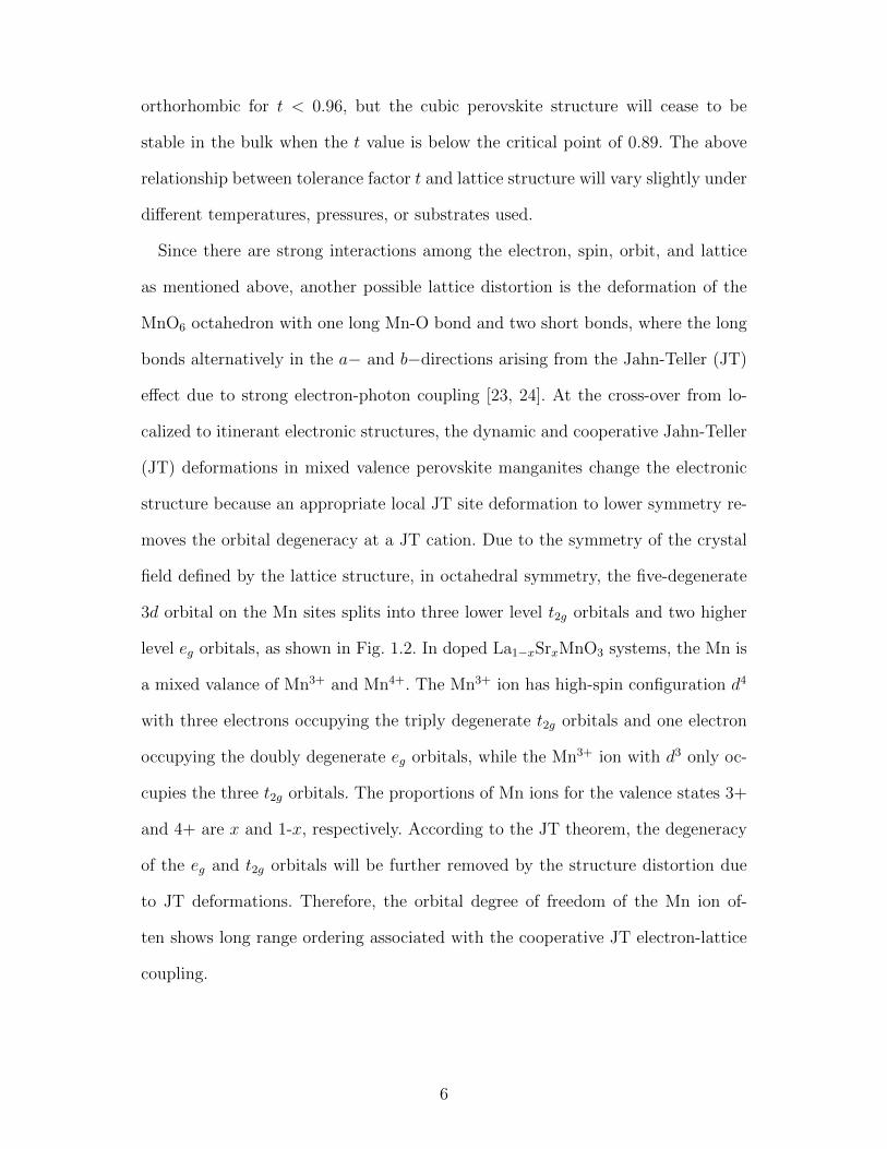
FIGURE 1.2: (a) The perovskite structure of manganites; (b) Field splitting of thefive-fold degenerate Mn3+ with d4 3d levels into lower t2g and higher eg levels, andfurther splitting of t2g and eg levels due to Jahn-Teller (JT) distortion. (c) Theshapes of these 3d orbitals.
The structure is ideally cubic with a B-O-B bond angle of 180 . The structure
will change to rhombohedral in the 0.96 < t < 1 range and further change to
5
orthorhombic for t < 0.96, but the cubic perovskite structure will cease to be
stable in the bulk when the t value is below the critical point of 0.89. The above
relationship between tolerance factor t and lattice structure will vary slightly under
different temperatures, pressures, or substrates used.
Since there are strong interactions among the electron, spin, orbit, and lattice
as mentioned above, another possible lattice distortion is the deformation of the
MnO6 octahedron with one long Mn-O bond and two short bonds, where the long
bonds alternatively in the a− and b−directions arising from the Jahn-Teller (JT)
effect due to strong electron-photon coupling [23, 24]. At the cross-over from lo-
calized to itinerant electronic structures, the dynamic and cooperative Jahn-Teller
(JT) deformations in mixed valence perovskite manganites change the electronic
structure because an appropriate local JT site deformation to lower symmetry re-
moves the orbital degeneracy at a JT cation. Due to the symmetry of the crystal
field defined by the lattice structure, in octahedral symmetry, the five-degenerate
3d orbital on the Mn sites splits into three lower level t2g orbitals and two higher
level eg orbitals, as shown in Fig. 1.2. In doped La1−xSrxMnO3 systems, the Mn is
a mixed valance of Mn3+ and Mn4+. The Mn3+ ion has high-spin configuration d4
with three electrons occupying the triply degenerate t2g orbitals and one electron
occupying the doubly degenerate eg orbitals, while the Mn3+ ion with d3 only oc-
cupies the three t2g orbitals. The proportions of Mn ions for the valence states 3+
and 4+ are x and 1-x, respectively. According to the JT theorem, the degeneracy
of the eg and t2g orbitals will be further removed by the structure distortion due
to JT deformations. Therefore, the orbital degree of freedom of the Mn ion of-
ten shows long range ordering associated with the cooperative JT electron-lattice
coupling.
6
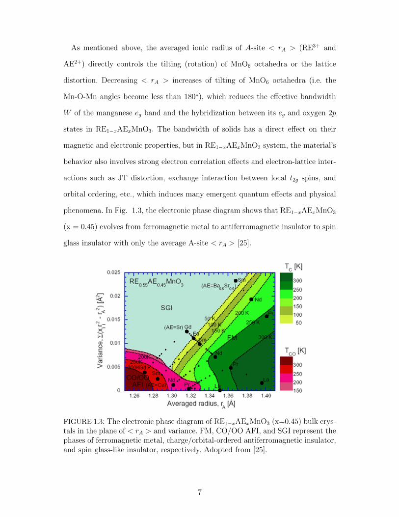
As mentioned above, the averaged ionic radius of A-site < rA > (RE3+ and
AE2+) directly controls the tilting (rotation) of MnO6 octahedra or the lattice
distortion. Decreasing < rA > increases of tilting of MnO6 octahedra (i.e. the
Mn-O-Mn angles become less than 180), which reduces the effective bandwidth
W of the manganese eg band and the hybridization between its eg and oxygen 2p
states in RE1−xAExMnO3. The bandwidth of solids has a direct effect on their
magnetic and electronic properties, but in RE1−xAExMnO3 system, the material’s
behavior also involves strong electron correlation effects and electron-lattice inter-
actions such as JT distortion, exchange interaction between local t2g spins, and
orbital ordering, etc., which induces many emergent quantum effects and physical
phenomena. In Fig. 1.3, the electronic phase diagram shows that RE1−xAExMnO3
(x = 0.45) evolves from ferromagnetic metal to antiferromagnetic insulator to spin
glass insulator with only the average A-site < rA > [25].
FIGURE 1.3: The electronic phase diagram of RE1−xAExMnO3 (x=0.45) bulk crys-tals in the plane of < rA > and variance. FM, CO/OO AFI, and SGI represent thephases of ferromagnetic metal, charge/orbital-ordered antiferromagnetic insulator,and spin glass-like insulator, respectively. Adopted from [25].
7

1.3 Physical Properties of Manganites
In these mixed valence manganites, subtle displacements in the crystal lattice can
induce a significant change in magnetism and electronic or thermal transport due
to the complex interplay between the lattice, spin, charge, and orbital degrees of
freedom [9, 17]. Various electronic, structural, and magnetic phase diagrams of
manganites are introduced and elucidated in the following section.
1.3.1 Phase Diagram of Manganites in Bulk
FIGURE 1.4: Phase diagram of RE1−xAExMnO3 systems with doping concentrationx and temperature T for representative distorted perovskites (a) La1−xSrxMnO3 (b)Nd1−xSrxMnO3 (NSMO) (c) La1−xCaxMnO3 (LCMO) (d) Pr1−xCaxMnO3 (PC-MO). There are several electronic and magnetic states: paramagnetic insulating(PI); paramagnetic metallic (PM); spin-canted insulating (SCI); charge-orderedinsulating (COI); antiferromagnetic insulating (AFI in the COI); canted antiferro-magnetic insulating (CAFI in the COI). Adopted from [9].
8

The bulk properties of CMR manganese oxides with perovskite structure have
been systematically studied during last two decades. Figure 1.4 shows the phase
diagrams of several types of manganites with different doping levels. The distorted
perovskite RE1−xAExMnO3 shows rich structural, electronic, and magnetic phases
with doping levels and temperature [9].
FIGURE 1.5: Phase diagram of La1−xSrxMnO3 (0 ≤ x ≤ 1). Crystal struc-tures, magnetic, and electronic states: Jahn-Teller distorted orthorhombic (O’),orthorhombic (O), orbital-ordered orthorhombic (O”), rhombohedral (R), tetrag-onal (T), monoclinic (Mc), hexagonal (H); ferromagnetic (FM), paramagnetic (P-M), antiferromagnetic (AFM), canted-AFM (CA); insulating (I) and metallic (M).Adopted from [76]
The parent compound LaMnO3 (LMO) is orthorhombic under uniaxial strain
conditions and shows an antiferromagnetic insulator (AFI) transition with TN ∼
140 K. Its ground state magnetic structure has ferromagnetic ab planes stacked an-
9
tiferromagnetically along the c axis. The application of pressure and charge doping
can induce metal-insulator transitions (MIT) [9], as well as huge magnetoresistance
(CMR ∼ 105 %) accompanied by magnetic transitions [10]. The strong interplay
between lattice distortions, transport properties, and magnetic ordering results in
rich and interesting physical properties and potential applications in doping LMO
systems. Besides MIT and CMR, doped LMO systems probe more fundamental
physics, such as double-exchange mechanisms, strong electron correlations, strong
electron-phonon interaction, cooperative JT distortions induced by orbital order
associated with Mn3+, and charge ordering, etc. Here, we briefly illustrate the com-
plex phase diagram of these manganites using La1−xSrxMnO3 as an example. In the
range of doping x < 0.1, La1−xSrxMnO3 is an insulating canted antiferromagnetic
structure (CI). With increasing doping level x, a ferromagnetic insulating phase
can be obtained at x ∼ 0.1. This FM phase keeps insulating up to x ∼ 0.17, in
which the double-exchange carrier is localized (Anderson localization) but can still
mediate the ferromagnetic interaction between neighboring sites and realize the
ferromagnetic state in a bond-percolation manner. Above 0.175, La1−xSrxMnO3
becomes metallic and the Curie temperature Tc dramatically increases with dop-
ing x from 250 K at 0.175 to the highest Tc ∼ 370 K at x ∼ 1/3. When doping x
reaches to 0.5, the metallic ferromagnetic state will be followed by an antiferromag-
netic insulating (or bad metal) state, where its electrical conductivity dramatically
decreases with the increase of Sr doping, as shown in Fig. 1.5 [76].
Magnetic and electronic properties of these manganites are governed by exchange
interactions between the Mn ion spins. The primary interactions arise from the n-
earest two Mn spins separated by an oxygen atom and are controlled by the over-
lap between the Mn d−orbitals and the O p−orbitals. Two-type distinguished ex-
change interaction models have been proposed to try to explain most of the magnet-
10

ic and electronic properties. One is the superexchange interactions, which depend
on the orbital configuration following the rules of Goodenough-Kanamori [28]. Gen-
erally, the superexchange interaction is antiferromagnetic for Mn4+ −O −Mn4+,
while it can be ferromagnetic or antiferromagnetic for Mn3+−O−Mn3+ [28]. An-
other is the exchange interaction of Mn3+ − O −Mn4+, named double exchange,
where the Mn ions can exchange their valence electrons by transferring the eg
electron of Mn3+ to the empty eg orbital of Mn4+ through the Op−orbital. The
probability of the eg electron transfer from Mn3+ to a neighboring Mn4+ is propor-
tional to t0cos(θ/2), where θ is the angle between the spin vectors of the Mn ion-
s [29, 30, 31]. Double exchange induces a metallic and ferromagnetic ground state in
manganites. The origin of the complex magnetic, electronic, and structural phase
diagrams of manganites versus the doping level x and the averaged ionic radius
of A-sites < rA > arises from the competition between double exchange ferromag-
netism and superexchange antiferromagnetism with different θ angular dependence
and TJ distortion. In addition, the crystal structure of the La1−xSrxMnO3 system
also undergoes a series of transitions from orthorhombic to rhombohedral to tetrag-
onal, even becoming monoclinic and hexagonal at some conditions, as shown in the
detailed phase diagram of single crystals of La1−xSrxMnO3 [76]. Figure 1.4 shows
that LSMO’s Tc of 370 is the highest Tc at optimal doping among the perovskite
manganites family. In addition, the bond theory indicates that the FM metallic
phase of LSMO has a half-metallic nature with fully polarized spin properties,
which has been demonstrated by spin-resolved photoemission measurements [14].
High Tc (above room temperature) and half-metallicity make LSMO one of
the most promising materials for metal-oxide-based spintronic devices, magneto-
tunneling junctions, magnetic memory, etc. Spintronics is an emerging field of
nanoscale electronics involving the detection and manipulation of electron spin
11

based on multilayer film structure and is one of the most promising technologies
for future low power computing and data storage [15]. For these device applications,
it is necessary to master the growth of high-quality thin films with well controlled,
tailored properties. To achieve these emerging oxide-based advanced multifunc-
tion devices, physical properties and growth mechanisms of epitaxially complex
manganese oxide thin films should be completely understood. Although there are
still numerous unresolved issues in these complex manganese oxides, especially in
their thin films and heterostructures due to involved strain at the surfaces and
interfaces which adds complexity, major progress has been made in the growth
techniques, structural characterization, and physical properties of the thin films
and heterostructures.
1.3.2 Physical Properties of Manganites Thin Films
Phase diagrams in Fig. 1.3, Fig. 1.4, and Fig. 1.5 show that the rich physical
properties associated with the multitude of competing ground states can be tuned
by doping, structural manipulations, or the application of the external stimuli,
such as magnetic/electric fields, light, and pressure, etc. The epitaxial growth of
oxide films have been attracting attention due to these superior properties that
could have great use in developing multifunction active devices. While significant
progress has been made in the epitaxial growth technology of oxides films in the
past decades, it has become increasingly clear that thin films, heterostructures,
and interfaces/surfaces of traditional metal oxides display much more diversity in
their physical properties and phenomena than in their bulks. Many novel physical
properties and functionalities that are absent in bulks emerge in heterostructures
or heterointerfaces due to broken symmetry and spatial quantum confinement at
the interface or surface, such as two-dimensional electron gas (2DEG) behavior
and superconductivity, etc. Figure 1.6 illustrates that the unique properties can be
12

deliberately introduced by surface structuring and interfacial engineering of thin
films and multilayer structures, providing additional degrees of freedom to tailor
functional properties.
Artificially engineering the interface of complex metal oxides is emerging as a
powerful approach to explore new physical phenomena in materials science and
electronics technology. For example, it has been found that the electronic re-
construction at the interface between tow non-magnetic band insulating oxides
LaAlO3/SrTiO3 (polar LAO layer and nonpolar STO layer) can give rise to a
high-mobility quasi-two-dimensional electron gas [32, 33], magnetism [34, 35] and
superconductivity [36, 37]. Charge transfer at the interface between Mott insu-
lating antiferromagnets LaMnO3 (LMO) and band insulator SrMnO3 (SMO) is
another example of interface engineering and can lead to localized ferromagnetic
ordering near the interface[38]. In addition, interfaces breaking inversion symmetry
can be polar, hence charge transfer can be induced at the interface to avoid poten-
tial divergence due to the polar catastrophe [19]. In LAO/STO and LMO/SMO
heterostructures, many theories and experiments [19, 38, 39, 40] show that the elec-
trical properties and even chemical compositions near interfaces can be changed
dramatically by charge transfer due to the polar nature of the structure.
The potential applications of CMR manganites in spin electronic devices or
magnetic sensors requires that their films be as well controlled in terms of physical
properties as their bulk counterpart [41]. However, as mentioned above, mangan-
ites have strong interplay between their charge, spin, orbital, and lattice, and their
physical properties are very sensitive to the structure, especially the MnO6 octa-
hedral distortions and O-Mn-O bond lengths and angles [42, 43]. Manganite thin
films show dramatically different physical properties than that of their bulks due to
uniaxial strain from substrates [49, 50, 51, 52, 53, 54, 55, 56, 57, 58, 59, 60], chem-
13

ical element diffusion at the interface [61, 62, 63], surface termination of the thin
film [64, 65], surface segregation and reconstruction [66, 67, 68, 69, 70], and oxygen
vacancies [71] during high temperature growth. It is important to understand the
growth mechanism of the complex manganese oxides, their chemical components,
and the structure of their thin films on the atomic scale, especially their interface
and surface because they have very different chemical and physical environments
than the interior of films.
FIGURE 1.6: Schematic diagram showing the additional manipulation approachesto symmetry and degrees of freedom of correlated electrons that can be engineeredat oxide interfaces.
1.3.3 Dead-layer in LSMO Thin Films
Since surface reconstruction, strain from the substrate, chemical element diffusion,
and charge distribution occur at interface and surface, perovskite manganites thin
films, especially ultra-thin films (< 10 unit cells), have dramatically different phys-
ical properties from that of their bulk [18, 72]. Previous results show that epitaxial
14

LSMO with 1/3 Sr doping thin films grown on single crystal substrates show a
non-ferromagnetic and insulating behavior when the thickness is less than certain
unit cells (∼ 2 to 3 nm for STO substrate, ∼ 10 nm for LAO with large lattice
mismatch) [64, 65], the type of thickness used for the magnetic metal layer in GM-
R spin-valve devices. In other words, LSMO ultra-thin films (in several unit cells
thickness) have serious degradation of both metallic and ferromagnetic functionali-
ties compared with the bulk, shown in the phase diagram in Fig. 1.4. The degraded
physical properties for these transition metal oxides thin films is referred to as the
dead-layer phenomenon [44, 72, 73, 74, 75]. This dead-layer phenomenon is an ob-
stacle which must be overcome before these manganese oxides can be applied for
next generation nanoscale spintronics devices.
FIGURE 1.7: Temperature dependent resistivity (a) and magnetization (b) forLa2/3Sr1/3MnO3 (LSMO) films with different thicknesses, grown on STO (001)substrates. Adopted from [27].
The transport and magnetic measurements of ultrathin LSMO grown on STO
(001) were systematically studied by M. Huijben et al. [27], and their results are
shown in Fig. 1.7. In the LSMO/STO (001) thin films, thick films above 13 u.c.
show a bulk-like metallic behavior over the temperature range, as well as a high
15

Curie temperature TC > 300 K. When the thickness of the LSMO films decrease to
less than 8 u.c, the LSMO films show insulating behaviors, as well as dramatically
decreasing electrical conductivity. At the same time, the saturation magnetization
and Curie temperature TC also dramatically decrease when thickness of films is
below the critical thickness 8 u.c. and is therefore defined as the dead-layer.
FIGURE 1.8: Schematic drawings of the lattice cell distortion of epitaxial film undertension (a) or compression (b). Adopted from [18]
Reducing the dead-layer behavior in LSMO thin films is of primary importance
and has been attempted through optimizing the lattice match between LSMO
film and substrate, growth conditions (Oxygen pressure), and tuning the interfa-
cial chemical stoichiometry, etc [44, 72, 73, 74, 75]. For instance, the pervoskite
LSMO (x ∼ 1/3) bulk and several common pervoskite substrates have different lat-
tice constants. Epitaxial LSMO films suffer compression or tensile strain from the
substrate based on their relative lattice constants, which can be characterized by
the degree of lattice mismatch ξ = [asubstrate − abulk]/asubstrate along the interface.
Positive ξ represents film suffering from in-plane tensile strain and compression
strain along the out-plane growth direction, which is illustrated in Fig. 1.8 [18].
16

The deformation of epitaxial films comes from substrate mismatch strain, which
can be characterized by utilizing high resolution transmission electron microscopy
(HRTEM) and X-ray diffraction (XRD) alongside a common θ − 2θ XRD scan or
in-plane Φ-scan.
FIGURE 1.9: Relationship between the thickness of dead layer and lattice mismatchbetween LSMO and substrates. (a) LSMO films suffer from compressive or tensilestrain based on different degrees of lattice mismatch between film and differenttype perovskite substrates; (b) Dependence of resistivity on temperature for LSMOfilms grown on substrates DSO, LAO, NGO, STO and NGO with 9 u.c. STO bufferlayer; (c) Thickness of dead-layer vs. the degree of lattice mismatch ε. Adoptedfrom [73, 75].
The most common substrates for CMR manganites are SrTiO3 (STO, a = 0.3905
nm, cubic), LaAlO3 (LAO, a = 0.3788 nm, pseudo-cubic), DyScO3 (DSO, or-
thorhombic with a = 0.5440 nm, b = 0.5717 nm, c = 0.7903 nm) and NdGaO3
17

(NGO, orthorhombic with a = 0.5426 nm, b = 0.5502 nm, c = 0.7706 nm). Lat-
tice mismatch influences the values of the parameters, as well as the distortion of
MnO6 octahedra, as illustrated in Fig. 1.9(a). The degree of lattice mismatch be-
tween LSMO films and LaAlO3 (LAO), NdGaO3 (NGO), SrTiO3 (STO), DyScO3
(DSO) are -2.1%, -0.3%, 0.8% and 1.9%, respectively [44, 73]. Although the intrin-
sic origin of the dead layer still remains controversial, it is clear that the lattice
mismatch between substrate and film plays an important role in physical proper-
ties of manganites. Many studies have found that, for thin films, lattice mismatch
caused the structural modifications at their interfaces that affected their magnet-
ic/electronic properties. Tensile or compressive strain induced distortion of MnO6
octahedra that alters the Mn-O bond length and the Mn-O-Mn angle subsequent-
ly changes the main physical properties supported by double exchange and the
Jahn-Taller effect. This can suppress ferromagnetism and reduce the ferromagnet-
ic Curie temperature (Tc), analogous to the results from reducing the thickness of
LSMO films growth on STO [50, 52, 54, 55].
The results of Fig. 1.9(b) show that both large compressive strain and tensile
strain will induce subtle structural change and consequently affect the physical
properties of LSMO films due to multiple comparable competing ground states
and strong coupling between the lattice and electrons. Based on double exchange
theory, the magnetic and electronic properties of LSMO are closely correlated to
the Mn−O−Mn bond angle and bond length of the MnO6 octahedral. The strain
on LSMO films from the substrate can be minimized, or even eliminated, by finely
tuning the lattice constant of the substrates, for example by adding additional
buffer layer between substrate and LSMO films. The relationship between the
thickness of the dead layer and the degree of lattice mismatch ε was summarized
in Fig. 1.9(C). For an LSMO film grown on NGO with a 9 u.c. STO buffer, the
18

strain effect on thin films can be minimized, but the film still has 3 u.c. of dead
layer [75]. Some groups suggest that the dead layer of ultrathin LSMO films are
due to phase separation related to structural inhomogeneities [52]. In addition, the
authors pointed out that the phase separation phenomenon in LSMO was on the
scale of a few nanometers, making it difficult to directly observe in experiment.
Other recent evidence has also suggested that the distortion of MnO6 octahedra
led to crystal-field splitting of eg levels and lowering the (3z2− r2) orbital over the
(x2 − y2) orbital due to Jahn-Taller distortion. This gives strong electron-lattice
coupling and causes orbital reconstruction at the interface [44, 46]. One study
suggests that the dead-layer is caused by the hole depletion near the interface
layers due to oxygen vacancy formation [71]. But in their results, the authors
speculate that oxygen vacancies are partly caused by interfacial electric dipolar
fields and lack any direct evidence to prove that oxygen vacancies exists at the
interface. Furthermore, in some studies of dead layer thickness determined from
transport and magnetization analysis, it was found that the critical thicknesses
of electric and magnetic dead layers were different [27]. The thickness thresholds
for metallicity and ferromagnetism are 7 u.c. and 4 u.c. respectively [27]. The
conductivity of films increases with the thickness of the film, and the conductivity
always is smaller than that of the bulk until the film is very thick ( > 40 u.c.).
Recently ,it was also suggested that the dead layer may be associated with polar
discontinuity-induced ion separation and electronic reconstruction at the interface
and surface [16, 19, 20].
1.3.4 Surface Termination of LSMO Thin Films
The free surface of LSMO films is also of particular interest in this research. Simi-
lar to the interface, the surface of oxides often display different stoichiometry and
chemical composition from their bulk due to the breaking down of long range
19

lattice periodicity, bonding, and chemical environment, resulting in an electrified
surface-like interface that also profoundly affects electronic transport. In addition,
it is normal for element segregation to take place at grain boundaries and surfaces
in complex oxides [66, 67, 68, 69] and binary or ternary alloys [77, 78]. Research
has shown that both the size difference and electrostatic interaction are respon-
sible for segregation [67]. When growing LSMO on STO or other substrates, we
would like to find what the final termination is for the LSMO films and whether or
not we can replicate the substrate terminations. The answer to these questions are
not only of concern when integrating half-metal LSMO thin films into spintron-
ics applications, such as magnetic tunnel junctions where physical properties and
functionalities are known to be largely determined by the chemical nature of the
interface, but also is important in uncovering the underling physical mechanisms of
these anomalous phenomena, and in the unique physical properties associated with
their surface and interface effects. For instance, it was found that the emergence of
quasi-two-dimensional electron gases (2DEG) and electric surface reconstruction in
STO/LAO requires that the STO be TiO2 terminated [16, 19]. Core-level photoe-
mission spectroscopy studies show that electric reconstruction associated with the
polarity discontinuity is the origin of the metallic electrons at the interface between
the two band insulators LAO/STO. Heterostructures of LAO/STO show metallic
conductivity with high mobility, as well as electronic reconstruction (Ti3+ signal)
only for LAO/STO with TiO2 termination, while LAO/STO with SrO termination
still show insulating behavior[16, 19].
1.3.5 Polarity Discontinuity at Interface
Extensive efforts have been directed into the study of the intrinsic origin of the
dead layer in LSMO/STO systems. Unfortunately, this problem still remains un-
resolved, and so far all attempts to completely eliminate the dead-layer behavior
20

have been unsuccessful. It seems that this unfavorable dead-layer is an inevitable
consequence of the underlying physical mechanisms related to its interfaces, sur-
faces, and the complex oxide growth mechanisms. Analogous to the LAO/STO
system, LMO or Sr-doped LMO is also a polar compound due to the existence of a
polarity discontinuity [40, 70]. Therefore, many theories and experiments suggest
that the polarity discontinuity at the interface may be the inevitable and intrinsic
force responsible for the redistribution of charge and ions related to the physical
properties and structure seen at the interface and surface, such as dead-layers, Sr
diffusion at the interface, and Sr segregation at the surface.
FIGURE 1.10: Schematic drawings of the polar discontinuniy and screening thedepolarizing field inside LAO. (a). the electrical potential divergence at theLAO/STO interface with TiO2 termination is avoided by electronic reconstruc-tion through adding half an electron to TiO2 termination layer in reducing thevalence of Ti4+ ; (b) the electrical potential divergence at the LAO/STO interfacewith SrO termination is also avoided by removing half an electron from the SrOtermination layer in the introduction of oxygen vacancies. Adopted from [19]
21

In heterostructures, there are interface dipoles resulting from band offset and
bond polarizations. Consequently, a larger energy cost will arise from these po-
lar discontinuities at abrupt heterointerfaces between layers with different polari-
ties. However, the system responds to this energy cost by changing it electrical or
structural properties, such as the creation of interface phases, or changing inter-
face roughness with the creation of oxygen vacancies, element migration, or diffu-
sion [19, 79, 80, 81]. It has been found that high-mobility electron gases correspond-
ing to an electronic restructuring at the LAO/STO interface and an unfavorably
roughening heterointerface are the results of avoiding an electrical potential diver-
gence due to the inevitable polar discontinuities. In LAO/STO with the interface
between polar and nonpolar layers, the polarity discontinuity induced potential
divergence can be avoided by redistribution of charge (electronic reconstruction)
and ions (such as oxygen vacancies, element diffusion, and segregation) across the
LAO/STO interface, which has been discussed in detail by N. Nakagawa et al., in
Fig. 1.10 [19].
1.4 Summary
Although many of studies and discussions related to the dead-layer phenomena
have been reported, including interface-induced strain through changing different
substrates, oxygen vacancy at the interface through changing oxygen growth pres-
sures, charge redistribution driven by electrostatic potential at the interface, and
even orbital reconstruction at interface, the origin of the dead-layer still remains
highly controversial. Most of the previous reported work focused only on the ex-
ternal relationship between the thickness of dead-layer and growth conditions or
different substrates. For LSMO thin films, detailed information about the precise
chemical components and structure of the interface and surface on the atomic scale
is still lacking. To better understand and explore the intrinsic origin of dead-layer
22

behavior, a series of in− situ characterization tools combined with complex oxide
growth capabilities, which are able to probe chemical components, surface/interface
terminations, and the morphology and structure on the atomic scale are required.
In this thesis, not only will the chemical composition and structure at interface
between LSMO and STO on atomic scale be determined, but also the termina-
tions and its thickness dependence will be analyzed quantitatively and discussed
based on the results of angle-resolved X-ray photoelectron spectroscopy (ARXPS)
and electron energy loss spectroscopy (EELS), as well as probing the local sur-
face electronic states and its temperature dependence using scanning tunneling
spectroscopy (STS).
23

Chapter 2Experimental Methods
2.1 Introduction
Most devices are based on thin films or heterostructues, whose properties are
strongly influenced by the film quality and surface/ interface qualities. Therefore,
the deposition of high-quality films and the characterization of those thin films,
during and after the fabrication process, is very important. For this thesis, films
were grown through Laser Molecular Beam Epitaxy (Laser-MBE) methods with
high powered laser beam ablation of the material from a target. Figure 2.1 depicts
the system in our lab, which combines three sections: a cleaving chamber, growth
chamber, and an in-situ analysis chamber. The cleaving chamber can be used to
load and cleave samples, and the growth chamber houses the Laser-MBE setup in-
cluding Reflection High Energy Electron Diffraction (RHEED). During the growth
process, RHEED enables us to directly observe the growth dynamics and surface
morphology.
Thin film characterization after the fabrication process can be divided into t-
wo categories: in− situ characterization and ex− situ characterization. After the
fabrication of films in our growth chamber, films were immediately in-situ trans-
ferred into the analysis chamber, which includes components for X-ray photoelec-
tron spectroscopy(XPS), Angle-resolved photoemission spectroscopy (ARPES),
low-energy electron diffraction (LEED) measurements, and scanning tunneling mi-
croscopy/spectroscopy (STM/STS), which allows us to probe the materials’ surface
structures, chemical compositions, and electronic properties. These characteriza-
tion tools detect electrons emitted or reflected from the surface, and therefore probe
the topmost 1∼10 nm of surfaces. Due to the surface sensitivity, those instruments
24

need to operate in high vacuum environments. By keeping the base pressure of
the analysis chamber to 2×10⁻¹⁰ torr, surface contamination due to the adsorp-
tion of residual-gas molecules can be omitted over a given time period. The sec-
ond group of possible measurements are the ex− situ characterizations, including
Scanning Transmission Electron Microscopy/Electron Energy Loss Spectroscopy
(STEM/EELS) and Physical Property Measurement System (PPMS), which pro-
vide information about the structure and chemical composition of the entire sample
and some transport measurements.
FIGURE 2.1: The system combines growth chamber and analysis chamber.
2.2 Film growth
2.2.1 Laser Molecular Beam Epitaxy (Laser-MBE)
Since the first laser was realized in 1960 by Maiman [82], many attempted to use
lasers in film growth. It was finally accomplished in 1987 when a Bell Communica-
25

tions Research group successfully grew epitaxial high-temperature superconductor
thin films [83]. After that, Pulsed laser deposition (PLD) has been widely used
in the film growth of high-temperature cuprates and other complex oxides. Using
this technique, novel materials that do not exist in nature can be designed and ex-
plored, such as superlattice films. The term Laser-Molecular beam epitaxy (MBE)
was introduced to describe a PLD system with layer-by-layer growth capabilities,
which also requires reflection high energy electron diffraction (RHEED) to monitor
film growth.
FIGURE 2.2: Schematic diagram of Laser-MBE setup
A typical setup for Laser-MBE is shown in Fig. 2.2. In the UHV chamber, six
targets can be mounted in the target carousel, which allows us to grow multilay-
ered films and superlattices. After being generated by the KrF laser and focused
through a focus lens, the high powered pulsed laser beam is guided onto a target,
which in turn delivers energy to the target, dissociating the target and forming a
26

plume. The plume expands rapidly with the fastest expansion direction along the
normal direction to the target surface. By placing a substrate facing the target,
materials of the plume can be deposited on the substrate to form a crystallized
film. This deposition process occurs far from thermal equilibrium, and therefore
the stoichiometry of the complex material can be preserved, which is the major
advantage of Laser-MBE.
Many experimental parameters can influence film properties. Laser parameters
such as energy, wavelength, pulse duration, and repetition rate can be altered to
affect growth. Other conditions including substrate temperature, background gas,
and pressure can also be important.
In our Laser-MBE system, we use a KrF excimer laser (COMPEx201) from
Lambda Physik. It produces 248 nm light with pulse durations of 25 ns, max-
imum pulse energies of 700 mJ, and maximum pulse frequencies of 10 Hz. The
commercially available premix gas (F2: 0.10%, He: 1.71%, Kr: 3.93%, Ne: 94.26%)
is used as the excimer gas. In the UHV chamber, by precisely controlling the leak
valve, the background gas can be changed, and gas pressure can be controlled
from 3×10⁻¹⁰ torr to 0.1 torr, which is limited by the pressure requirements of
the RHEED gun. The distance between the target and substrate is fixed at about
4 cm. The homemade heater allows us to change the substrate temperature from
room temperature to 900 C.
2.2.2 Reflection High Energy Electron Diffraction (RHEED)
RHEED is essential to Laser-MBE growth, which is a surface sensitive technique
used to monitor the growth by probing the surface topography. The RHEED setup
is schematically shown in Fig. 2.3(a). It consists of an electron gun and a phosphor
screen to record the diffracted pattern. A high energy electron beam approaches the
sample at a grazing angle, which for our system is about 2.5. Some of the diffracted
27

electrons reach a phosphor screen and form a RHEED diffraction pattern, which
is then captured by a charge-coupled device (CCD) camera. Our RHEED gun
produces an electron beam energy up to 35 keV, which creates electrons with a
mean free path of about 25A. With an incidence angle of 2.5 , the penetration
depth is then about 1 for our samplesA, which is as small as one atomic layer and
makes RHEED a surface sensitive diffraction technique.
FIGURE 2.3: (a) Schematic diagram of RHEED setup. (b) RHEED patterns andAFM images during growth of one unit cell layer. (c) Ideal layer by layer filmgrowth [84].
Figure 2.3(a) shows some RHEED patterns and response images recorded by
Atomic Force Microscopy (AFM). Due to the grazing angle of the electron beam,
RHEED patterns are very surface sensitive, which only gathers information from
the surface layer of the sample. According to the surface structure, surface mor-
phology, and the incident electron wavelength, the diffracted electrons interfere
and create specific diffraction patterns, which provides information about not only
the surface symmetry but also the surface topography.
28

The relation between the surface topography and RHEED pattern is shown in
Fig. 2.3 (b) and (c). In Fig. 2.3 (b), due to the substrate being covered by a
complete monolayer before growth, the RHEED pattern intensity is strong. With
the deposition of a film, an incomplete monolayer begins to form, so the intensity
of the spots decreases. As the film grows, it eventually completes a full monolayer,
and as it does, the intensity of spots becomes strong again. Figure 2.3 (c) shows
an ideal layer-by-layer growth process and corresponding oscillation curve. During
film growth, RHEED is used to provide information on the film flatness and crys-
tallization. By tracking the intensity of the spots of the reflected pattern, we can
observe the RHEED oscillations, which is used to evaluate the growth rate, the
number of grown layers, and directly observe the growth dynamics.
2.3 In− Situ Characterization
FIGURE 2.4: Theory predicted mean free path depends on electron energy (dashline) and mean free path of electrons in solid as a function of their energy. [85].
The analysis chamber contains some surface sensitive instruments, which enable
us to in−situ probe the structure, chemical composition and electronic properties
29

of the film surface to several layers deep. For different equipment, the probing depth
differs depending on the sample, beam energy, and direction. Many experiments
can be performed to measure the attenuation length in different materials with
different energies, where the attenuation length is equivalent to mean free path.
Figure 2.4 shows a collection of experimental determinations of mean free path as
a function of energy for different metals.
2.3.1 Low Energy Electron Diffraction (LEED)
LEED is a surface sensitive technique for the determination of the surface structure
of crystalline materials. Figure 2.5(a) shows a schematic diagram of LEED setups,
which shows a collimated beam of low energy electrons produced by an electron
gun which reach a fluorescent screen, where a LEED pattern formed by diffracted
electron spots can be observed. The energy of the electron beam ranges from 20
to 200 eV, which therefore determines the electron’s wavelength via the de Broglie
relation:
λ = h/p = h/mv = h/√
2mE (2.1)
where λ is the wavelength of a particle with momentum p, mass m, velocity v, and
energy E. h is Planck’s constant. From this equation, for an electron with kinetic
energy of 150.4 eV, its wavelength is 1 A. That is:
λe[A] =√
150.4/E[eV ] (2.2)
Similarly, the wavelength of electrons with kinetic energy 20-200 eV ranges from
2.7-0.87 A, which is comparable with the lattice constant of a crystal. The pene-
tration depth is several angstroms, estimated from Fig. 2.4, which enables LEED
to be an excellent probe for the surface structure of a crystallized sample. Quali-
tatively, the LEED diffraction pattern can be analyzed to get information on the
30

symmetry of the surface structure. Figure 2.5 (b) is the LEED pattern of parent
Sr3Ru2O7 at 190 eV, where the surface has a√
2×√
2 reconstructed pattern. For
quantitative analysis, the electron beam energy can be changed, which produces a
shifted diffraction pattern. Simply by changing the wavelength of electrons, the in-
tensity of different spots can be tracked and recorded as a function of incident elec-
tron beam energy to generate Intensity-Voltage (I-V) curves shown in Fig. 2.5(c).
These are used in theoretical calculations to determine accurate information on the
atomic surface positions. Full dynamic calculations are computationally costly, so
a perturbational tensor LEED (TLEED) approximation has been developed and
implemented by Rouse and Pendry [86, 87, 88, 89]. In the process of I-V curve
refinement, the so-called reliability factor (RP -factor) is used to quantitatively e-
valuate the quality of a certain model between the theoretical and experimental
I-V curves. The RP -factor used in this work is one developed by Pendry [90]. RP
is based on logarithmic derivatives of the IV spectra intensity I(E):
L =1
I(E)
dI(E)
dE(2.3)
When the IV curve is near a minima with I(E) ≈ 0, a singularity occurs in the
logarighmic derivative. To avoid such singularities, a Y function is introduced:
Y =L
1 + L2V 2oi
(2.4)
where Voi is the imaginary part of the optical potential that is used to keep the
function finite within the range of ±1/2Voi. While an energy dependence of V oi(E)
is introduced in the calculation of the theoretical IV spectra as outlined above, a
constant average value (Voi = - 4eV ) is assumed in the calculation of RP .For a
particular I-V beam, RP is given by:
31

Rp =
∫(Yth − Yexp)2dE∫(Y 2
th + Y 2exp)dE
(2.5)
where Yexp and Yth are the Y functions for the experimental and theoretical beams
respectively, and Voi is the imaginary part of the electron self-energy.
If RP= 0 there is perfect correlation between the theoretical and experimental
I-V curves. RP=1 means that theory and experiment are completely uncorrelat-
ed. The lower RP factor acquired, the better is surface structural determination.
Usually, an RP of about 0.3 is sufficient to corroborate a certain structure.
FIGURE 2.5: (a) Schematic view of LEED setup.(b) LEED diffraction pattern ofSr3Ru2O7 measured at 190 eV. (c) LEED-IV curve of (1,0) diffraction spot.
The LEED used in this project is an Omicron LEED. It works in our UHV
system where the pressure is maintained at 3 × 10⁻¹⁰ Torr at room temperature.
LEED I-V data acquisition is done with a high resolution camera and LabView
programmed software.
32

2.3.2 Angle resolved X-ray Photoelectron Spectroscopy (ARXPS)
Based on the photoelectric effect, photoelectron spectroscopy uses photons to ionize
the sample and emit electrons, which can be analyzed to study the composition
and electronic state of a sample surface. Traditionally, there are two types: X-
ray photoelectron spectroscopy (XPS) and Ultraviolet Photoelectron Spectroscopy
(UPS). UPS creates electrons of energy 10-45 eV to study valence levels, which is
not utilized here. XPS is based on a soft x-ray source with a photon energy range of
200-2000 eV to analyze core levels, which can be used to determine the elemental
composition, empirical formula, chemical state, and electronic state of the elements
that exist within a material. The standard detection limits range from 0.1 to 1.0
atom%.
FIGURE 2.6: Schematic drawing of a typical ARXPS setup with photon source.
Figure 2.6 depicts the schematic of an ARXPS setup, which shows a beam of
photons produced by the X-ray source incident on the sample. The X-rays are
usually generated by high velocity electrons bombarding Al or Mg anodes, which
produce emission photon energies of 1486.7 eV or 1253.6 eV respectively. To get a
33
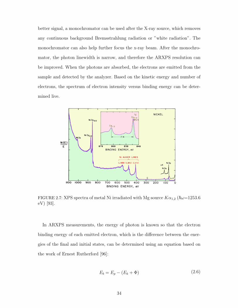
better signal, a monochromator can be used after the X-ray source, which removes
any continuous background Bremsstrahlung radiation or ”white radiation”. The
monochromator can also help further focus the x-ray beam. After the monochro-
mator, the photon linewidth is narrow, and therefore the ARXPS resolution can
be improved. When the photons are absorbed, the electrons are emitted from the
sample and detected by the analyzer. Based on the kinetic energy and number of
electrons, the spectrum of electron intensity versus binding energy can be deter-
mined live.
FIGURE 2.7: XPS spectra of metal Ni irradiated with Mg source Kα1,2 (~ω=1253.6eV) [93].
In ARXPS measurements, the energy of photon is known so that the electron
binding energy of each emitted electron, which is the difference between the ener-
gies of the final and initial states, can be determined using an equation based on
the work of Ernest Rutherford [96]:
Eb = Ep − (Ek + Φ) (2.6)
34

where Eb is the binding energy (BE) of the electron, Ep is the energy of the
X-ray photons being used, Ek is the kinetic energy of the electron as measured by
the instrument, and Φ is the work function of the spectrometer. For the analyzer,
the work function changes and therefore needs to be calibrated with a standard
sample, which for our system is done with a clean Au sample with a 4f peak.
FIGURE 2.8: The bonding energy of C 1s peaks with different chemical states.
The X-ray photoelectron spectrum consists of a few basic types of peaks: (1)
peaks from core levels, (2) peaks from valence levels, (3) peaks from X-ray excited
Auger decay (Auger series), and (4) other peaks, such as multiple splitting, ghost
peaks, and satellite peaks [92]. Figure 2.7 is a typical XPS spectrum for metallic
Ni, which contains: the valence band (3d, 4s) at EB of several eVs; very weak 3p,
3s, and 2s peaks at about 66, 110 and 1008 eV respectively; Auger peaks arising
from x-ray induced Auger emission marked with LMM, LMV, and, LVV; and an
intense 2p peak and its satellite peaks around 860 eV, which is further expanded
and shown in the inset of Fig. 2.7. Here the descriptions of the XPS peaks (4s,
35

3d, 3p, 3s, 2s, and 2p) are based on the electron configuration of the atoms. The
2p peak is split into 2p1/2 and 2p3/2 arising from spin-orbit coupling. Two possible
states, characterized by the quantum number j (j = l + s = l ± 1/2), arise when
l 6=0, where the intensity ratio between two peaks with j+ = l+1/2 and j− = l−1/2
is given by (l + 1)/l, based on the degeneracy of each spin state [95]. Spin-orbit
splitting values can be found in a variety of databases [93, 94], which are needed
when fitting spectra.
Satellite peaks are important phenomenon in XPS quality determination for
many reasons. Surface charging, shake-off and shake-up effects (i.e. a sudden change
in Coulombic potential as the photoejected electron passes through the valence
band), plasmon electronic excitation, and multiple X-ray source photon energies
can all observed with satellite peaks.
Chemical shifts are another possible signature in XPS, which includes final state
and initial state chemical shifts. The final chemical shifts are due to charging ef-
fects in an insulating sample, which can cause the peaks to shift to higher binding
energies. The initial state chemical shifts can be used to distinguish different oxida-
tion states and chemical environments. For the same element, the binding energy
of a core electron can be different for different samples, and the difference can be
from one tenth of an eV to a few eV. The exact binding energy of an electron
is determined by the core level of the electron, the oxidation state of the atom,
and the local chemical and physical environment. For an atom, a higher positive
oxidation state means a higher positive charge for the atom and more Coulomb
interaction, which therefore requires the most energy for electrons to escape. As a
result, a higher positive oxidation state means the core level has a higher binding
energy, which is shown in Fig. 2.8. Three different carbon chemical bondings can
be clearly identified for C 1s peaks. Higher oxidation states have higher binding
36

energies in C 1s core levels, though the energy differences are within 1 eV. The
line widths are also different, which is related to the lifetime of the photoelectrons
coming from the specific core levels. Although the binding energy can be changed
due to the chemical shift, the binding energy difference between the two spin-orbits
of one element remains the same.
In X-ray photoelectron spectroscopy, the contribution to the signal intensity IA
by the layer thickness dz at the depth z is given by [97]:
dIA(z, θ) = TAσAnA(z)exp(−z/λAcosθ)dz (2.7)
where TA is the transmission coefficient of the analyzer, σA is the photoionization
cross-section, λA is the inelastic mean free path (IMFP) of analyzed photoelectrons,
and θ is the emission angle shown in Fig. 2.6.
Further assuming that the value λA depends only on the kinetic energy of pho-
toelectrons, we obtain the intensity IA of an element A [98]:
IA(θ) = TAσA
∫ ∞0
nA(z)exp(−z/λAcosθ)dz (2.8)
The XPS intensity ratio IA/IB for elements’ A and B core level peaks is defined
as [99]:
IA(θ)
IB(θ)=TAσA
∫∞0nA(z)exp(−z/λAcosθ)dz
TBσB∫∞0nB(z)exp(−z/λBcosθ)dz
(2.9)
To quantitatively analyze ARXPS data IA(θ)/IB(θ), Eq. 2.9 and relative param-
eters are used. σ can be found in XPS handbooks and T is related to the analyzer
used. IMFP λ is the only unknown parameter here.
37

The predictive equation for the Inelastic mean free path (IMFP) used in this
thesis is called TPP-2M, which is name after S. Tanuma, C. J. Powell, and D.
R. Penn. The TPP-2M equation is a function of electron energy E (eV) and is
described by [100]:
λ =E
E2p [βln(γE)− (C/E) + (D/E2)]
(2.10)
The parameters for IMFP calculations include the following:
β = −0.10 + 0.944(E2p + E2
g )−1/2 + 0.069ρ0.1
γ = 0.191ρ− 1/2
C = 1.97− 0.91U
D = 53.4− 20.8U
U = Nvρ/M = E2p/829.4
Ep = 28.8(Nvρ/M)1/2
Here, Ep is the free-electron plasmon energy (in eV).
A Specs X-ray source XR 50M with Al anode (Al Kα 1486.6 eV), Specs FOCUS
500 X-Ray Monochromator, and a Specs PHOIBOS-150 analyzer are equipped for
ARXPS in our lab. The overall energy resolution for the XPS spectra is 0.15 eV,
which is based on the X-ray source line width. The kinetic energy of a photoelectron
is relatively low (<1.5 KeV), so only a low number of electrons which escape from
the top 3 to 30 nm of a material are analyzed.
2.3.3 Scanning Tunneling Microscopy/Spectroscopy (STM/STS)
Scanning tunneling microscopy (STM) was developed by Gerd Binnig and Hein-
rich Rohrer at IBM in 1982, garnering the 1986 Nobel prize for their invention
[101]. STM is a technique based on quantum tunneling, which is the phenomenon
through which a particle can ”tunnel” through a barrier that it classically could not
38

surmount. STM can image surfaces in real space with the atomic resolution. Figure
2.9 (a) shows images from the omicron STM in our lab, and (b) is a schematic view
of an STM setup. When the tip and sample are separated by distances on he order
of nanometers and a bias is applied between them, electrons can tunnel through
the vacuum separating them. The tunneling current can be monitored. A feedback
control is essential in STM to keep the current at some constant by moving the tip
height. When the tip moves in plane, the distance between the tip and sample can
change, so to keep the current constant, the vertical position of the tip will change
by utilizing the feedback control. A typical STM image is recorded by monitoring
the tip position, the vertical height z as a function of location (x,y).
FIGURE 2.9: (a) An image of Omicron VT-STM. (b) Schematic view of STM setup.
In the quantum mechanics, electrons have wavelike states described by wave
function ψ. In 1D cases, ψ satisfies Schrodinger’s equation:
− ~2m
d2
dz2ψ(z) + U(z)ψ(z) = Eψ(z) (2.11)
where ~ is the reduced Planck’s constant, z is the position, m is the mass of an
electron, E is the electron energy, and U(z) is the energy barrier. In classical
39
mechanics, when U(z) > E, the particle cannot cross the barrier. However, in
quantum mechanisms, the Eq. (2.11) has a solution in this case:
ψ(z) = ψ(0)e−kz (2.12)
Here, k =√
2m(U − E)/~. U is related to the work function and any modifica-
tion to the tunneling barrier due to the crystallographic orientation, sample local
topography, tip sample angle, etc. If the applied bias V U , k ≈√
2m(U)/~,
and the tunneling probability of an electron behind the barrier of width d can be
given by:
|ψ(d)|2 = |ψ(0)|2e−2kd (2.13)
Then the tunneling current is proportional to the probability of electrons inside
the barrier:
I ∝Ef∑
Ef−eV
|ψn(0)|2e−2kd (2.14)
This negative exponential function of the current I and distance d between tip
and sample is the key for the atomic resolution. For example, when U = 4 eV, the
decay constant k is about 1A−1. When tip position z changes 1A, the current decay
changes about e2 = 7.4, nearly one order of magnitude in the current. Thus, any
topographic height change will be amplified through the tunneling current, which
gives atomic resolution for STM images.
In addition to imaging the surface topography, STM allows one to probe the
local density of states (LDOS) on surfaces. When the bias V is small enough, at a
location z, the LDOS (ρz,E) of the sample is defined as:
ρz,E =1
V
E∑E−V
| ψn(z) |2 (2.15)
40

So that
I ∝Ef∑
Ef−eV
LDOS(d,E) (2.16)
The current depends not only on z but also the integration of the LDOS at an
energy window near the Fermi surface in Eq. 2.16, which indicates that STM images
are related to both the morphology of the surface and the electronic properties
of the surface. Equation 2.16 clearly shows the relation between the tunneling
current I, the bias voltage V , and the tip-sample distance z. Therefore, three
kinds of spectroscopies can be used: 1) I − z curves with constant V , which can
be used to obtain the local work function; 2) V − z curves keeping I constant ;
3) with z constant, scanning I − V curves, which are widely used and reflect any
conductance variations over the sample. Further, by applying two different biases,
STM can probe the filled states with positive bias, and the empty states with the
negative bias [103].
If the derivative of I with respect to the bias V is taken, the following equation
can be obtained:
dI
dV∝ LDOS(d,E) (2.17)
Equation (2.17) shows the capability of STM to probe the electronic properties
of sample surfaces. Technically, dI/dV as a function of applied voltage can be
obtained by the 1st derivative of the I/V curve. The direct and more precise
way to detect the dI/dV signal is done using a lock-in amplifier. A small high
frequency sine signal is added to the bias. This small modulation causes a response
in the tunneling current. By using a lock-in amplifier, the first harmonic response
frequency can be extracted, which is proportional to dI/dV .
However, dI/dV is V-dependent, which may distort the features in the STM.
Stroscio et. al. proposed a simple but effective solution to this problem [102]. They
41

normalized dI/dV by dividing it by I/V , which yielded d(lnI)/d(lnV ), effectively
canceling out the V dependence. However, this normalization is both unnecessary
and undesirable at small bias, in which case, the I/V curve is well behaved and
(dI/dV)/(I/V) is identically equal to unity for ohmic systems and carries no infor-
mation.
Our variable temperature scanning tunneling microscopy (VT-STM) is a new-
ly designed Omicron combination of STM and QPluse AFM (Atomic force mi-
croscopy), which allows imaging of both conductive and insulating surfaces, and
can reveal electronic inhomogeneities and local structural reconstructions.
2.4 Ex-situ Characterization
By using the previous in-situ measurements, we are able to study film surfaces.
However, for information from deeper inside the film or near the interface, other
techniques are needed. Transport and magnetic measurements using Dr. Rongying
Jin’s equipment were obtained, and transmission electron microscopy was done at
Brookhaven National Lab.
2.4.1 Scanning Transmission Electron Microscopy/Electron EnergyLoss Spectroscopy (STEM/EELS)
Scanning transmission electron microscopy (STEM) is a type of transmission elec-
tron microscope (TEM) that is widely used to directly image the position of atoms
in crystallized samples.
The history of TEM can be traced back to 1925 when Louis de Broglie first
theorized the wave-like properties of electrons [104]. The first STEM was realized
in 1938 by Baron Manfred von Ardenne in Berlin[105]. In the 1970s, Albert Crewe
developed the field emission gun, and created a modern STEM using this technique
coupled with a high-quality objective lens [106]. He also demonstrated STEM’s
ability to image atoms using an annular dark field detector.
42

An illustration of the STEM instruments used is schematically shown in Fig.
2.10(a). Similarly to optical microscopy, STEM uses an electron beam as the ”light”
source and a magnetic lens instead of an optical lens. By using a condenser lens,
the electron beam can be focused to a small spot, though it is not small enough
for atomic resolution. The aberration corrector is essential for further focusing
the beam to an ultra narrow spot smaller than 1 A, which is the main factor
limiting the resolution of STEM. By changing the scanning coils, the highly focused
electron beam is raster-scanned across the sufficiently-thin material. Various types
of scatterings are collected as a function of position.
FIGURE 2.10: (a) Schematic view of STEM setup. (b) HAADF and (C) ABFimages of LSMO film on STO(001).
High angle annular dark field (HAADF) imaging is widely used in STEM, which
is formed by very high angle beams and incoherently scattered electrons in a ring-
shaped circumference from 90 to 370 mrad. The image intensity of the HAADF
43

image is approximately proportional to Z2, which typically results in easier visual-
ization of heavy elements. Because the collected electrons are incoherent, the atom
positions can be directly measured from the images. For many important materi-
als, light elements such as oxygen, nitrogen, lithium, and hydrogen are common
components, but these are unable to be identified with HAADF images.
The Annular bright field (ABF) images is another method in STEM, which
preferentially receives the ring-shaped circumference from 11 to 23 mrad. Different
from HAADF images, ABF images easily and clearly see lightweight elements.
However, ABF imaging is less advantageous in some applications due to it’s strong
dependence on both thickness and focusing, making interpretation of ABF images
more complicated.
TEM was originally designed to give structural information about a specimen.
However, the interaction between incident electrons and sample allows STEM to
also probe chemical information and electronic structure. When electrons travel
through a specimen, some of them can be inelastically scattered. Inelastic interac-
tions include phonon excitations, inter and intra band transitions, plasmon excita-
tions, inner shell ionizations, and Cherenkov radiation. An electron spectrometer
can be used to measure any changes in the energy distribution of the inelastically
scattered electrons, which is the crux of Electron Energy Loss Spectrum (EEL-
S) [107] techniques. The energy loss is due to inner-shell ionizations, which are
characteristic for different elements, and this enable EELS to detect elemental
components and atomic bonding states in a material.
Cross-sectional STEM samples were cut into ∼ 80 nm thicknesses by a focused
ion beam (FIB) with Ga+ ion milling, and then nanomilled with Ar+ ions to
remove surface damage and further thin the sample to about 50 nm. All the samples
were studied under a double-aberration-corrected 200 kV JOLE ARM equipped
44

with a dual-energy-loss spectrometer. Dural EELS mapping across the interface
was collected with a dispersion of 1eV. The STEM conditions were optimized for
EELS spectroscopy with a probe size of ∼ (spot size 4), a convergence semi-angle
of 20 mrad, and a collection semi-angle of 88 mrad. Line-scanning EELS spectra
were obtained across the interface with a step size of 0.12 A, and a dwell time of
0.05 s/pixel.
2.4.2 Physical Property Measurement System (PPMS)
The resistivity of the film as a function of temperature ρ(T ) is measured by a
commercial Quantum Design Physical Properties Measurement System (PPMS)
shown in Fig. 2.11(a). PPMS is designed to perform a variety of measurements,
such as determining specific heat, thermal transport, alternating current (AC)
susceptibility, and transport measurements.
FIGURE 2.11: Instrument of Quantum Design PPMS. (b) Schematic diagram offour probe method.
By using PPMS, the direct current (DC) resistance R can be measured using
a four-probe method. The setup is shown in Fig. 2.11 (b), which consists of the
probe arrangement, sample constant current generator, and digital voltage. The
four probe method is a widely used standard for the measurement of resistivity,
due to its ability to ignore contact resistance in the measurement. The film sample
45
is grown on an insulating substrate with length a and thickness h, which can
range from a few to several hundred layers. Four probes are arranged linearly in a
straight line, the two outside probes having constant current I passing through and
the middle two measuring the potential drop V across distance L. The resistivity
ρ of the film is calculated by
ρ = R · (a · h)/L =V
I· (a · h)/L (2.18)
Compared with two probe methods, four probe measurement results are more
accurate and can avoid the influence of ohmic contacts.
2.4.3 Summary
An important condition for modern materials physics and nanoscience is control
of materials to atomic dimensions. For complex oxides, Laser-MBE has proven to
be a growth technique through which the deposited material can be controlled
at the atomic scale. Stoichiometric transfer, high deposition rate, and tunable
energy of the arriving particles are parameters which enable us to control the film
growth with layer-by-layer growth feasible for various complex oxides to a surface
roughness of only one unit cell. ARXPS and LEED can be used to determine
the surface chemical composition and structure of the thin films and provide some
insight into the their effects on the eventual film properties. For information on the
interior, both for chemical composition and structure of the thin films, we need
to use STEM/EELS to analyze the samples. The surface morphology and local
electronic properties of samples can be studied by using STM , while PPMS enables
us to probe properties of the whole film. Combining these in− situ and ex− situ
analysis tools, we are able to systemically study and evaluate the properties of thin
films in detail.
46

Chapter 3Substrate treatment and LSMO filmgrowth
3.1 Introduction and motivation
SrTiO3 (STO) is an insulator with a band gap of 3.2 eV. The structure of STO
is cubic perovskite with a lattice constant of a= 3.905 A. Self-doping with oxygen
vacancies or element doping by Nb result in an n-type semiconductor, which makes
STO suitable for in− situ analysis to avoid any charging effects. STO is a widely
used substrate material for the growth of thin films and heterostructures due to its
compatible cubic perovskite structure and lattice constant. Many interesting new
properties appear at the interface of STO with other transition metal compounds,
including two-dimensional electron gas and superconductivity which appear at the
interface between STO and LaAlO3 films [32, 36].
STO (001) has a controllable termination layer with either TiO2 or SrO. The
atomically flat TiO2 terminated surface can be obtained by using a HF buffer
solution etching and in − situ or ex − situ annealing [110]. SrO terminated STO
is usually obtained by high temperature annealing [109] or depositing a SrO layer
on a TiO2 (001) surface termination [111].
STO plays an important role in the film growth and resultant properties. A
theoretical calculation suggests that a termination layer of STO can change the
interface electronic and magnetic properties of STO and La2/3Sr1/3MnO3 interfaces
[112]. More importantly, surface defects, polarity, reconstruction, and termination
layers could strongly affect the properties of films grown on STO.
La2/3Sr1/3MnO3 (LSMO) is an attractive material for rich physics and potential
technological application [14, 15]. LSMO has rhombohedral structure, with an an-
gle of 90.26 and a lattice parameter of 3.88 A. However, some possible applications
47

are limited by the LSMO ultra-thin film properties, with different behaviors mani-
festing depending on the substrates and growth conditions [27, 44, 50, 52, 72, 113,
114]. By studying the relation between the growth modes, oxidation levels, and
material properties, the optimized growth conditions for LSMO films were found
[75], which enable us to minimize the extrinsic influences on the LSMO properties
and probe more intrinsic characteristics.
In this chapter, we investigate the influence of growth and oxygen concentra-
tion on the transport properties of LSMO films grown on STO. Epitaxial oxide
thin film growth requires the use of crystalline substrates. Achieving atomically
flat substrates is essential for high quality film growth. In section 3.2, different
treatments of STO are presented, and the best treatment of TiO2 terminated STO
(001) is determined using ARXPS and STM. The growth and structural properties
of LSMO films on STO substrates are described by using experimental tools XRD,
RHEED, and STM in section 3.3, which also includes transport studies of these
films.
3.2 The treatment of SrTiO3 substrate
In this thesis research, Only LSMO thin films grown on STO(001) were system-
atically studied. STO was chose as substrate because STO is cubic (a=3.905A)
with only 0.5% lattice mismatch with LSMO (a=3.88 A). For the transport and
magnetic measurements, the substrates used were non-doped STO. For the XPS,
LEED, STM/STS, and STEM/EELS measurements, 0.1wt% Nb doped STO was
used as the substrate. All STO substrates are single crystals bought from CrysTec
GmbH of Germany, which have a size of 5 mm × 5 mm × 0.5 mm.
To get an atomically flat substrate, STO was sonicated in acetone for 2 minutes,
then Ethanol for 2 minutes, then Milli-Q water for 2 more minutes. The sample
is then dried using ultra pure N2 gas and then etched in a buffer NH4FHF (BHF)
48

solution (from Alfa Co.) for 30s. Finally, the sample is dried again and annealed in
the vacuum chamber or tube furnace. To study the two different annealing meth-
ods, we studied and compared the morphology and surface chemical composition
of STO with different treatments.
First, we annealed STO in the growth chamber with 10−4 Torr Ozone at different
temperatures. When the annealing temperature increased to about 900 C, the
STO surface morphology changed, showing straight step edges with the step height
∼ 0.39 nm, as seen in Fig. 3.1 (a) and (b), which suggest that STO annealed in
the chamber has a single termination.
FIGURE 3.1: (a) STM image and (b) height profile of STO annealed at 900 C for1 h with 10−4 Torr Ozone. (c) Angle resolved spectra of Ti 2p and Sr 3p peak.(d) Angle dependence of intensity ratios Ti2p/Sr3p, degassed in UHV for 1 hrat 100 C (Rectangle), and annealed in 10−4 Torr Ozone for 1 hr with 500 C(circular) and 900 C (triangle). The pentagram is the theory result of STO withTiO2 termination.
49

To study chemical composition of STO, ARXPS was performed with the STO
substrate. The actual data collection was taken with an angle step of 5. Selected
raw data with 0, 15, 30, 60 and 80 are shown in Fig.3.1(c). From the raw data,
for different angles, the intensity ratio of Ti2p/Sr3p can be determined, which can
be plotted with the angle dependence of these intensity ratios in Fig.3.1(d). Figure
3.1(d) shows that the change in intensity for different core levels are not monotonic,
but rather have a sudden change at 18.4 , 26.5 , 45 , and 63.4 , which is related
to forward scattering contributions based on the crystal structure.
TABLE 3.1: Parameters to calculate the IMFP of characteristic curves for STO.
Valence electrons number Nv 24 Band gap Eg (eV) 3.25
Density ρ ( g.cm−3) 5.12 Molecular weight M (g/mol) 183.49
TABLE 3.2: List of parameters of Sr 3p, Sr 3d, Ti 2p and O 1s core levels for STOARXPS calculation.
Element Shell Cross section Mean free path Transmission coefficient
σ λ (A) T
Sr 3p 6.62 22.85 40.42
Sr 3d 5.05 24.80 39.10
Ti 2p 7.81 20.07 42.56
O 1s 2.92 19.01 43.30
For TiO2 terminated STO, the angle dependence of intensity ratios Ti2p/Sr3p
can be calculated by Eq. 2.9. First, to calculate the inelastic mean free path (IMF-
50

P), Table 3.1 contains the related parameters needed. Combing Equation 2.10 and
Table 3.1, the IMFP for different cores of STO are calculated and list in Table 3.2,
which includes other parameters for relative intensity ratio calculation.
FIGURE 3.2: The morphologies of STO substrates are annealed at different tem-perature (a) 800 C (b) 900 C (c) 950 C and (d)1000 C.
For TiO2 terminated STO, the theory calculated angular dependence of the
intensity ratio of Sr3p/Ti2p is drawn as open pentagram in Fig. 3.1 (d), which
shows obvious increasing at larger emission angles. Different from the theory result,
experimental Ti2p/Sr3p shows a slight drop at larger emission angle, which is likely
due to missing Ti or partially left over Sr on the surface. One group reported that
TiO2 termination of STO can be achieved by annealing STO at 750 C with 7.5 ×
10−5 torr O2 [108]. Although our STM pattern and line profiles also suggest that
STO treated at 900 C has a single termination, ARXPS demonstrates that STO
51

annealed in vacuum chamber with a low oxygen/Ozone environment cannot have
perfect TiO2 termination, as it is substantially Ti deficient.
To get better TiO2 terminated STO, we then attempted to anneal the substrate
in the furnace with an O2 base pressure of ∼ 1.45 PSI for 3 hr, with warming and
cooling at a rate of 100 C/h, and then degas it in the UHV chamber with ∼ 300
C before finally preparing for STM and ARXPS measurements.
FIGURE 3.3: Surface morphology, structure and termination characterizations ofSTO ex−situ annealed at 900 C for 3 hr with O2 ∼ 1.45 PSI. (a) STM image; (b)1×1 LEED pattern; (c) and (d)Experimental data and theoretical calculation basedon TiO2 or SrO termination of the angle dependent intensity ration of Ti2p/Sr3pand Ti2p/Sr3d.
The obtained surface morphologies of STO with respect to different annealing
temperatures are displayed in Fig.3.2. For STO annealed at 800C for 3 hours, the
step edge is still not straight shown in Fig.3.2 (a), indicating that an annealing
52
temperature of 800 C is not enough. When the substrate annealing temperature
was increased to 900 C, the step edge straightened out, as seen in Fig.3.2 (b).
However, when the annealing temperature keeps increasing, large-scale STM im-
ages of STO (c) and (d) show obvious low-lying regions with about 0.5 u.c. height
difference along the terraces edging, which indicates the appearance of local SrO
termination [109].
For the STO substrates ex − situ annealed with the high O2 pressure, 900C
is the best treatment temperature. The surface morphology clearly shows more
straight terrace step edges with the atomically flat surface shown in Fig.3.3(a).
There is no reconstruction of the STO surface, which is confirmed by the sharp 1
× 1 LEED pattern in Fig.3.3 (b). To further check the termination, 900C treated
STO is characterized by ARXPS, and the results are shown in Fig.3.3 (c) and (d).
From the raw ARXPS date for STO, the intensities of different core peaks (Ti2p,
Sr3p, and Sr3d) can be calculated, which further can be used to calculate experi-
mental results for the angle dependent intensity ratio of Ti2p/Sr3p (black) shown
in Fig. 3.3(c). Different from the in − situ treatment of STO, for the ex − situ
treated STO, the ratio of Ti2p/Sr3p increases at larger emission angle, and the
drops in the ratio around 18 and 45 are due to the forward scattering effect.
Comparing the experimental results with the theoretical calculation results of the
angle dependence of Ti2p/Sr3p with TiO2 (red line) or SrO termination (blue line),
we can see that the 900 C treated STO (001) obviously has TiO2 termination.
The experimental result and theoretical calculation of Ti2p/Sr3d as the function
of emission angle are also shown in Fig. 3.3(d), and these also support a TiO2
termination conclusion.
In summary, we investigated the surface of HF-etched SrTiO3 (001) substrates.
It is found that in−situ annealed STO with lower Ozone pressure has a Ti deficient
53

TiO2 termination surface. Although, after treatment at 900 C inUHV chamber
with lower pressure Ozone, STO shows an atomically flat surface in STM and the
line profile shows a 1 u.c. terrace height difference, ARXPS shows an obvious Ti
defect, which indicates that STO treated with low gas pressure cannot achieve
both the correct stoichiometry and an atomically flat surface at the same time.
To achieve better substrates, ex − situ annealing of STO with a higher O2 base
pressure at ∼ 1.45 PSI was performed. After a 900 C treatment temperature,
the surface of STO was checked using STM imaging. Further, the surface shows a
1×1 LEED pattern with no reconstruction. By comparing the experiment results
and theory calculations, ARXPS also shows that the ex − situ annealed STO is
terminated with TiO2 without any Ti deficiency, which is different from in− situ
low O3 pressure treated STO.
3.3 High quality LSMO film growth
In this section, the growth of the LSMO thin films is described. With perfect TiO2
terminated STO, obtained with the method described in the previous section, the
growth of the thin films using PLD is described. In− situ RHEED measurements
were used to reveal the two-dimensional (2D) layer-by-layer growth mode for LSMO
film growth. Finally, the surface morphology was further characterized by STM and
LEED, which shows smooth and well ordered surfaces.
3.3.1 LSMO film growth
LSMO films were deposited on TiO2 terminated STO (001) by using our Laser-
MBE system with a stoichiometric LSMO target. A KrF excimer laser ( 248 nm)
at a laser frequency of 3 Hz and laser energy of 1 J/cm2 was used. The spot size
of the laser beam on the target was 0.021 cm2. During the growth, a mixture of
99% O2 + 1% O3 gas was applied.
54

To obtain layer-by-layer growth for LSMO films, an optimized growth tempera-
ture window was explored and was found to at ∼ 700 C. When higher tempera-
ture is used for film growth, the RHEED oscillation became unstable after a short
time. While, for the lower growth temperature, the film growth became 3D, which
indicates poor crystal quality of the films. As the results, the LSMO growth tem-
perature was chosen to be around 700 C, which maintains a layer-by-layer growth
mode.
FIGURE 3.4: (a) RHEED pattern of STO before film growth. (b) RHEED intensityoscillation pattern at various oxygen partial pressures.
With the optimized growth temperature, layer-by-layer epitaxial growths of
LSMO films were obtained. Figure 3.4 (a) shows the 2D RHEED diffraction pat-
tern for the STO substrate. By monitoring the variations in RHEED intensity, the
LSMO film growth dynamics can be studied. A layer-by-layer growth mode was
obtained for all pressures ranging from high vacuum (10−6 Torr) to high pressure
around 130 mTorr, which can be observed in the RHEED intensity oscillation in
Fig. 3.4 (b). The oscillatory behavior of RHEED also demonstrates that, keep-
55

ing other conditions the same, higher gas pressure results in slower LSMO growth
rates, which is read from the period of the intensity oscillations.
FIGURE 3.5: Temperature dependent resistivity for LSMO films with differentthicknesses grown at 80 mTorr. [75]
For the LSMO films grown with 80 mTorr pressure, the temperature dependence
of the resistivity for variable films thicknesses is given in Fig. 3.5. Thicker films
show a bulk-like metallic behavior below ∼ 360 K, approaching or achieving the
resistivity of the bulk in the thicker samples, similar to other group results [27].
The Curie temperature of the films increases with film thickness up to ∼ 360 K
for the 60 u.c. film, which is close to the Curie temperature ∼ 369 K in the bulk
crystals. When the film thickness decreases, the LSMO film resistivity increases
drastically for the whole temperature range. For 6 u.c. LSMO film, the continuous
resistance decreases as we increase the temperature, which indicates that the 6
u.c. LSMO film is insulating. However, for 7 u.c. LSMO, the resistivity behavior is
completely different from 6 u.c., where now the LSMO resistivity decreases with
the temperature below around 250 K, indicating metallicity.
56

LSMO film transport properties strongly depend on the growth pressure and
film thickness. LSMO films with different pressures are grown, and the trans-
port properties are measured. Our group’s previous results show that, for certain
growth pressures, LSMO films become less metallic with a decrease in thickness
[75]. Below a certain critical thickness (tc), LSMO films are ”dead” and become
insulators. Higher Ozone growth pressures enhance the conductivity and favor a
metallic ground state, through which it can be concluded that oxygen deficiency
plays an important role in the dead layer, and drives the films to be more insu-
lating. Although the dead layer decays with increasing growth pressure, the dead
layer cannot disappear, and is minimized at 6 u.c., which can be achieved with a
growth pressure of ≥ 80 mTorr. When the growth pressure is ≥ 80 mTorr, oxygen
deficiency is not the key issue for LSMO films. Due to this optimization, 80 mTorr
is chosen as the oxygen pressure for our film growth.
FIGURE 3.6: (a) RHEED images in the (100) direction for STO substrate. (b)RHEED images in the 20 u.c. LSMO films. (c) Typical RHEED intensity os-cillations for 20 u.c. LSMO growth on STO (001) (d) Zoom in of the RHEEDoscillations from (c) .
57

Figure 3.6 shows the experimental RHEED results for the STO substrate and 20
u.c. LSMO film growth. Figure 3.6 (a) is a typical experimental 2D RHEED pattern
obtained from a single crystal STO (001), which clearly shows a good crystallized
substrate and flat surface. During film growth, by tracking the reflection spots
in Fig. 3.6 (b), the RHEED oscillations can be obtained, which is shown in Fig.
3.6(c). Based on the RHEED oscillation, the growth rate is calculated to be 46.5
± 0.5 s/u.c., which strongly depends on the growth conditions. A significant phase
shift in the RHEED oscillations between the specular spot at (0,0) and the other
two spots at (0, 1) and (0, -1) can be observed. Given the same incident electron
energy and growth conditions, phase shift depends on the incidence angle [115].
If we closely examine the first layer growth of LSMO film in the RHEED os-
cillations in Fig. 3.6 (d), we can see that an extra maxima appears between two
oscillation peaks of the specular spot, which can only be observed within a small
region of the glancing angle of the incident beam. To better understand the extra
maxima, quantitative results for each peak and the extra maxima are obtained
and shown in Fig. 3.7. Within the error bar, for different layers, the growth times (
i.e. specular peak positions ) are the same at about 46.5 s. For the extra maxima,
the growth time, which is calculated by the difference between the current maxima
and previous peak, seems to gradually change with thickness. However, consider-
ing that the time when oscillation minima appear is near the extra maxima, and
therefore affects the position of the maxima, the smallest peak at position 3 u.c.
provides the most trustworthy extra maxima time of 23.1 ± 1 s, which is about
half of the 1 u.c. growth time. Although extra maxima were observed, the extra
maxima for LSMO film growth only appear in the first several layers, when com-
pared with the dynamical RHEED theory calculation and explained as a perfect
monolayer-by-monolayer growth mode [115]. The RHEED pattern also changes
58

dramatically, which could be related to the mixed termination, though this aspect
requires further study.
FIGURE 3.7: Specular and extra maxima growth time for different thicknesses.
3.3.2 LSMO film quality characterization
The optimized LSMO film growth conditions are determined to be ∼ 700 C with
80 mtorr mixed Ozone gas. In this section, the high quality of our LSMO films are
demonstrated, which in turn minimizes extrinsic influences on films properties.
As mentioned above, the transport measurements in Fig. 3.5 already show a
dead layer of 6 u.c., which currently is minimized for LSMO films grown on a STO
(001) substrate. Higher gas pressure cannot further reduce the thickness of dead
layer, which shows that oxygen deficiency does not drastically influence LSMO
films grown under optimized conditions.
In addition to the layer-by-layer growth mode for LSMO films being confirmed
through RHEED oscillations in Fig. 3.4, the surface morphology of the LSMO
thin films were further investigated by STM images. Different from transport mea-
surements, which measure LSMO films grown on non-doped STO, for the STM
59

scanning, a more conductive 0.1wt% Nb-doped STO substrate was used. Figure
3.8 (a) shows the surface morphology of a 12 u.c. LSMO ultrathin film. Clear ter-
races with a width of about 70 nm are observed. A single step height of ∼ 0.39
nm can be found in our STM image, indicating a single termination surface. For
layer-by-layer growth, it is difficult to determine the exact moment to stop growth,
which can cause some small extra patches to be found on the surface, as seen in
our image.
FIGURE 3.8: (a) The STM image of the surface morphology of a 12 u.c. LSMO film.(V=1.0 V, I = 20 pA, T = 300 K ) (b) LEED pattern of 12 u.c. LSMO film at RTat 95 eV. (c) HAADF-STEM image near the interface of 40 u.c. LSMO grown onSTO (001) taken along [110]. The dish line indicates the interface between LSMOfilm and STO substrate.
Figure 3.8 (b) depicts the LEED pattern at 95 eV for an LSMO film, which
demonstrates the good crystallization of the film. The 1×1 characteristic and lack
of any reconstruction pattern can be observed on the LSMO films’ surface. The
60

microscopic structure was further investigated by STEM in Fig. 3.8 (c), which is
part of a high-resolution TEM image of the cross-sectional structure of 40 u.c.
LSMO films grown on STO (001). The film was crystalline and the LSMO/STO
interface is seen to be very sharp. Looking at the entire image, no obvious peak
splitting due to the small mismatch was found, indicating that the LSMO film is
very high quality and uniformly epitaxial.
3.4 Summary
In this chapter, we investigated different treatments to achieve the most atomically
flat TiO2 termined STO (001) possible. Before annealing, the STO substrate was
cleaned and HF etched. It is found that, for in− situ treatment with low oxygen/
mixed Ozone gas pressure, the annealed STO substrate has an oxygen deficient
TiO2 termination surface. This surface is not stable, and so the 1×1 surface eas-
ily reconstructs when the annealing temperature is raised above 500 C. Using
ARXPS, we can prove that, different from the in− situ treatment, the ex− situ
annealing with high oxygen pressure can keep the film stoichiometric and main-
tain an atomically flat substrate surface at the same time, making it the better
treatment for STO (001) substrates.
We also optimized the growth conditions of LSMO films on STO substrates by
changing parameters such as growth temperature and Ozone pressure. It is found
that an ideal layer-by-layer growth can be achieved with a growth temperature of
∼ 700 C. At the growth temperature of ∼ 700 C, a minimized dead layer of 6 u.c.
can be achieved by growing with mixed Ozone at≥ 80 mTorr. With these optimized
growth conditions, the atomically flat surface of LSMO films is confirmed by STM,
which is also proved to be no reconstruction by LEED. The STEM results further
demonstrate the high quality of LSMO films, which are well-crystallized and no
obvious disorder and dislocation. By using this optimized substrate treatment and
61

growth process, we are able to minimize the extrinsic effects on LSMO films, which
will allow us to further investigate the intrinsic properties of LSMO films.
62

Chapter 4Layer-by-layer composition
4.1 Introduction and motivation
In the last few decades, it has become increasingly clear that surfaces, interfaces,
thin films, and heterostructures of transition metal oxides (TMOs) display a rich
diversity of fascinating properties that are related, but not identical, to their bulk
phenomena [116, 42, 117, 118]. New states of matter, which are inaccessible in
the corresponding bulk compounds, have been discovered at interfaces. Examples
include surface-tailored purely electronic Mott transitions [119, 120], interface-
induced superconductivity [32], two-dimensional electron gases [36], orbital recon-
figuration [121], and interface-controlled ferroelectric polarization [122], as well as
dimensional crossover driven metal-insulator transitions [33, 123]. Such emergent
phenomena herald a possible new generation of oxide-based electronics [124]. Oxide
devices involve the fabrication of thin films, superstructures, and junctions. The
design of virtually all electronic devices begins with an understanding of interface
barrier formations, electronic/magnetic structures, and control of the structure,
composition, and interface [125].
Understanding the nature of the emergent phenomena in these artificially struc-
tured materials requires thorough study of their structure-property relationships.
While the essential starting point should be the characterization of lattice struc-
ture and chemical composition, the termination (final atomic configuration) of
each deposited layer, and possible induced distortion at the interfaces, as well
as imperfections such as vacancy, defects, impurity, etc., are crucially important
for emergent properties. Even in the most studied TMO system, LaAlO3/SrTiO3,
many proposed mechanisms for these observed phenomena are still hotly contest-
63

ed, including polarity effect [19], cationic mixing [126, 127], and intrinsic doping
due to the existence of oxygen vacancy [128, 129], as well as thickness-dependent
polar distortion [130] and the exponential decay of lattice relaxation effects [131].
The exciting observations, as well as many remaining unresolved issues, point to a
consensus that many TMO interfaces are more complex than previously realized,
and motivate new approaches to both materials growth and characterization.
In this chapter, we report on our study on the chemical composition varia-
tion with atomic layer precision in ultrathin films of doped manganite material
La2/3Sr1/3MnO3 (LSMO) using a combination of in− and ex− situ microscopy
and spectroscopy. Our results reveal that there is a substantial increase in the Sr
concentration from its bulk value both at the interface and in proximity to the film
surface. The deviation at the interface with the STO (001) substrate is mainly due
to single unit cell intermixing, while the deviation in proximity to the film surface
is because of Sr surface segregation. As the substrate surface is terminated, the
LSMO film surface experiences a gradual self-organized conversion from a MnO2
to (La/Sr)-O layer termination with increasing thickness. Such layer-by-layer vari-
ation in composition and its dependence on film thickness should have an immense
impact on the physical properties of epitaxial films and heterostructures.
Manganite perovskites have been extensively studied for more than half a cen-
tury due to their potential applications in solid electrolytes, magnetic sensors,
spintronics, and even catalysts, as well as due to their rich physics such as colossal
magnetoresisitance, charge ordering, half-metallicity, and phase separation, all of
which are related to the close coupling among the charge, lattice, orbital, and spin
[8, 132, 133, 134]. One particularly interesting manganite is LSMO because of it
has the highest Curie temperature Tc (∼ 369 K in the bulk crystals) and the most
itinerant electronic character among the manganites [135], showing functionalities
64

for promising technological applications. Ironically, for LSMO ultrathin films, its
metallic states and ferromagnetic ordering are greatly suppressed [136, 27], which
is very different from the bulk and is usually referred to as a ’dead layer’. The
critical thickness of the dead layer depends on the strain and oxygen stoichiometry
[75]. However, the intrinsic origin of the dead layer still remains highly contro-
versial. It has been suggested that the dead layer is caused by nanoscale phase
separation due to spatial structural inhomogeneity [137], but why such inhomo-
geneity occurs in ultrathin films only is unclear. Others have suggested that the
dead layer is related to orbital reconstruction because of the MnO6 octahedron dis-
tortion at the interface [44, 138]. Due to the rich doping-dependent phase diagram
including the metal-insulator transition, ferromagnetism, antiferromagnetism, and
charge ordering in La1−xSrxMnO3 [76], chemical composition variations can be vi-
tal in understanding the different properties between films and the bulk. Although
Sr segregation at surfaces has been suggested [66, 139, 140, 141], there is no clear
picture about the layer-by-layer chemical composition profile in LSMO films.
4.2 LSMO film interface composition from TEM
By using PLD, epitaxial LSMO films with different thicknesses were deposited
on atomically flat TiO2 terminated 0.1 wt% Nb-doped STO (001) substrates. The
growth conditions for high-quality LSMO films are discussed detailed in the chapter
3, the quality of which has been confirmed through RHEED, LEED and STM.
The well-ordered structure and high quality of the LSMO films can be further
confirmed by scanning transmission electron microscopy (STEM). Figure 4.1(a)
displays high-angle annular dark field (HAADF) STEM image taken along [110]
for 40 u.c. LSMO. These images are atomic number(Z)- contrast images, powerful
for structure determination and defect identification such as dislocated cores. For
LSMO, the atomic numbers are: La(57) > Sr(38)>Mn(25)> Ti(22) > O(8). Under
65

these conditions, the bright dots observed in the right part of Fig. 4.1(a) correspond
to the projection of LSMO films. The left part of STEM figure depicts the STO
substrate. From the STO portion, it is worth noticing that these two types of atoms
give rise to the different kinds of contrast dots. The brighter dots seen in the STO
exclusively correspond to the projection of Sr atomic columns, whereas Ti columns
are imaged very weakly. Similarly, for the LSMO films, the bright dots correspond
to the projection of Sr/La atomic columns, while the weak dots are Mn atoms.
FIGURE 4.1: (a) HAADF-STEM image and (b) ABF-STEM of 40 u.c. LSMO grownon TiO2 terminated STO interface along [110]. A zoom-in ABF-STEM (Right)images and a structural model from the marked area shows the position for La/Sr,Mn and O atoms.
Although the light element O cannot be observed in HAADF-STEM images,
both light and heavy element can be imaged through ABF-STEM, as shown in
Fig. 4.1(b). By comparing with the HADF-STEM images, we can are clearly see
the extra atoms in the ABF images, which correspond to the O atoms. The right
inset is a zoom-in image from the marked area. For the marked area, a structural
model with the position for La/Sr, Mn, and O atoms is also given, which shows
that the Mn and O atoms are not along a straight line nor is the Mn-O bond angle
180o.
66

Both the HAADF- and ABF-STEM images in Fig. 4.1 solidly confirm the conti-
nuity of the perovskite stacking sequence without obvious dislocation or defect by
surveying over different areas and films. We also checked 8 u.c. and 4u.c. LSMO
films grown on STO in the [100] direction in Fig. 4.2, both of which still show
an ordered structure. For all HAADF-STEM images, the unambiguous Z-contrast
difference in the brightness of imaged A-site atoms (Sr in STO side vs. La/Sr in
LSMO side) indicates atomically sharp interfaces between the STO and the LSMO
films.
FIGURE 4.2: (Color online) HAADF-STEM image for La, Sr, Ti and Mn ofLSMO/STO interface for (a) 8 u.c. taken along and (b) 4 u.c. taken along [100],respectively.
To achieve more quantitative interface concentration results, electron energy loss
spectroscopy (EELS) is applied to the LSMO films. After background subtraction
and de-convolution for removing the multi-scattering effects, the La M4,5, Sr L2,3,
Mn L2,3 and Ti L2,3 edges of EELS spectra were integrated to provide elemen-
tal profiles, which are superimposed onto the corresponding atomic sites in the
HAADF images shown in Fig. 4.3. Here, (a), (b), (c) and (d) are results for 4
different local areas of one same sample.
67

The stacking sequence near the LSMO/STO interface is the first information
obtained from EELS in Fig. 4.3. In the previous section, the HADF-STEM images
demonstrated the continuity of the perovskite stacking sequence of LSMO films on
the STO substrate. As a result, there are two possible configurations: (1) ...-SrO-
TiO2-(La/Sr)O-MnO2-... and (2) ...-TiO2-SrO-MnO2-(La/Sr)O-... At the interface
of 8 u.c. LSMO/STO, the La signals (blue) propagate further into the interface
than the Mn signals (purple), demonstrating that all LSMO films have stacking
sequence ...-SrO-TiO2-(La/Sr)O-MnO2-... at the interface. This result is consistent
with the substrate treatment which achieved TiO2 terminated STO.
FIGURE 4.3: Profiles of chemical composition as a function of distance for 4 differ-ent areas of the 8 u.c. LSMO/STO interface extracted from the La-M edge, Ti-Ledge, and Mn-L edge.
Although very sharp interfaces are observed in the HADF-STEM images in Fig.
4.1 and Fig. 4.2, the elemental profiles still show a 1 - 2 u.c. interfacial intermixed
region and a significant deviation of Sr concentration at the interface. For the
B-site, about 20% Mn is detected in the TiO2 termination layer at -0.5 unit cell
68

(u.c.); about 45% and 15% Ti intermixes into the first and second MnO2 layers
with positions 0.5 u.c. and 1.5 u.c. respectively.
FIGURE 4.4: (Color online) The concentration profiles for La and Sr as a functionof distance (unit cells) from the interface obtained from Fig4.3.
To quantitatively analyze the Sr/La ratio evolution, the atomically resolved
concentrations are derived from the elemental intensity profiles, as shown in Fig.
4.4, which are based on the 4 different samples of the EELS results in Fig. 4.4 and
calibrated by the 40 u.c. LSMO film results. Since the 40 u.c. LSMO shows the
same transport/magnetic properties as the LSMO bulk with an Sr doping of 0.33,
the composition of the interior layers in the 40u.c. film can be used as the standard
for all film calibration.
To get more a precise Sr/La ratio, we need to get rid of some extrinsic influ-
ences. First, the areas including the step, which always exist in the substrate and
are shown in Fig. 3.1, need to be avoided. Figure 4.5 (a) is a schematic view of the
STEM specimen including the terrace. The cutting and step direction is along b,
and the STEM/EELS measurement direction is along a. For the STO substrates,
the terrace width is about 70 nm. While, for the STEM specimen preparation, typi-
69

cal sample thickness is about 40 nm. The probability of the EELS/STEM including
the step information is strongly dependent on the sample cutting direction. If the
STEM specimen is cutting along the step direction, there is about a 57% chance
for the specimen to include step information in the STEM and EELS results.
FIGURE 4.5: (Color online) (a) The STEM specimen includes a step. The cuttingand step directions are along a; the STEM/EELS measurement direction is alongb. (b) Based on sample (a) and (c) in Fig. 4.4 results and simple model of step,fitting results for sample (b) and (d) in Fig 4.4 are given.
If the step-included specimen is measured by STEM/EELS, the interface con-
centrations will not be intrinsic. Figure 4.4 illustrates this, including four sets of
data, where in the first (La/Sr)O layer at the interface, the Sr concentrations in
samples (a) and (c) are about 0.6 while samples (b) and (d) have a 0.8 doping.
Another possible explanation for the samples differences are that the 8 u.c. LSMO
film is not uniform. Other samples grown under the same conditions, such as 40
u.c. and 4 u.c. films, do not have such problems, which indicates that nonunifor-
mity is intrinsic from the sample. Using the (a) and (c) sample results to model
the step, the fit results with steps and samples (b) and (d) are shown in Fig. 4.5
(b). The error bar is 0.05, which is based on the Sr concentration deviation from
the averaged results in the region from 2 u.c. to 6 u.c. in the Fig. 4.4. Figure. 4.5
70

(b) demonstrates that the difference in interface concentrations between samples
(a), (c) and (b), (d) can be explained by the sample having a step, as found in our
results.
FIGURE 4.6: (Color online) Averaged EELS elemental concentration profiles forLa/Sr as a function of distance (unit cells) from the interface between (a) 40 u.c.,(b) 8 u.c., (c) 4 u.c. LSMO, and STO substrate.
After eliminating the step influence, three different EELS results for different
films were averaged, as shown in Fig. 4.6, which give us more precise information.
At the interface, the gradual change in Sr concentration can effectively reduce the
diverging potential force from the polar discontinuity based on the electrostatic
potential calculation [70]. For both thick and thin films, Sr concentrations reach
∼ 0.60 with about 80% deviation from the interior composition, which should be
71

insulating as well as antiferromagnetic [142]. In the second (La/Sr)O layer (at 1
u.c.), for the thick 40 u.c. film, Sr dramatically drops to the bulk value of ∼ 0.35
with about 6% deviation from its interior layers. While, for the thin films with 8
u.c. and 4 u.c., Sr concentrations still have a considerable deviation of 33% from
the 0.33 value.
To produce a more quantitative difference at the interface of the thick and thin
films, we fit the Sr profiles with the exponential function:
fSrz = b+ δI · exp(−zd/lI) (4.1)
where z indicates the position of the Sr/La-O layer (z=0 u.c. at the first inter-
face layer), b is 0.33, and lI is related to the decay length. The difference can be
directly reflected in the fitting parameters. The Sr profiles can be fit well with this
exponential function with a fitting parameter lI = 0.94 ± 0.18 for the 8 u.c. film.
Although only three data points for 4u.c. can be used for fitting, which cannot
give good fitting results, the ultrathin films of 4 u.c. and 8 u.c. have a very similar
Sr depth profile at the interface, so that the 4 u.c. and 8 u.c. LSMO films should
have similar decay lengths at the interface. For 40 u.c., the fitting parameter lI is
given by 0.26 ± 0.06. The Sr concentration decay in thin films (4 u.c. or 8 u.c.) is
much slower than that of thick films (like 40 u.c.), which could be due to influences
from its surface. The fitting parameters for Sr profiles near the interface are given
in Table 4.1.
TABLE 4.1: Fitting results for Sr profiles near the interface of LSMO films
Film δI lI/d Sr
4 or 8 u.c. 0.31±0.02 0.95±0.18 0.33+0.31 · exp(-z/0.95)
40 u.c. 0.22±0.01 0.26±0.06 0.33+0.22 · exp(-z/0.26)
72

4.3 LSMO film surface composition from ARXPS
During the STEM sample preparation, a focused ion beam could damage the sur-
face without any covering layers, which gives an unpredictable error bar not in-
cluded in Fig. 4.6. In the Fig. 4.6, for the 8 u.c. LSMO film, two layers of Sr/La
at positions 7 u.c. and 8 u.c. near the surface are not plotted because the EELS
data for these two layers are not good, which is due to the aforementioned surface
damage. This may cause the absolute value of surface Sr to be less reliable.
FIGURE 4.7: (a)Schematic diagram of ARXPS measurement. (b) raw ARXPS spec-trum of Mn2p, Sr3d and La4d core levels for 65u.c. LSMO films grown on TiO2
terminated STO substrate.
To obtain more precise surface information, the surface composition is deter-
mined by in− situ ARXPS with the experimental schematic shown in Fig. 4.7(a).
By changing the emission angle θ, angle-dependent XPS spectra are obtained. Fig-
ure 4.7(b) shows the raw XPS spectra containing Mn 2p, Sr 3d and La 4d core
peaks for 65 u.c. LSMO films as a function of emission angle θ. Due to the finite
inelastic mean free path of electrons, by vary emission angle θ, the XPS spectra
provide chemical composition information from different depths.
73

To quantitatively analyze the chemical composition of an LSMO film near the
surface, the angle dependence of the relative intensities of Sr3d/La4d is used.
After subtracting the Shirley background from the raw data, the core level (Mn2p,
Sr3d, and La4d) intensities for each emission angle can be calculated. Further, the
angular dependence of the LSMO Sr3d/La4d intensities are obtained in Fig. 4.9
(a). For films with thickness ≤ 10 u.c., due to the Sr signal intensity partially
coming from substrate STO, the fittings of ultra-thin films are disturbed and less
reliable, and are not discussed here.
For the thick film fitting of Sr3d/La4d intensities, the equation for the XPS
intensity ratio RAB(θ) of two atoms core level peaks (A and B) must be used [99]:
RAB(θ) =IAIB
=σA ∗ TAσB ∗ TB
∑i f
Ai exp(
−idλAcos(θ)
)∑j f
Bj exp(
−jdλBcos(θ)
)(4.2)
Here, σA is the photoionization cross section of element A, T is the transmission
coeffcient of the analyzer, d is the interlayer spacing, λ is the inelastic mean free
path of the photoelectrons, θ is the emission angle with respect to the surface
normal, and fAi is the atomic fraction of element A at the ith layer. For top surface
layer, the i is 0. fAi is assumed to has an exponential segregation profile:
fAi = b+ δS · e−id/lS (4.3)
Where b is the bulk fraction of Sr (0.33) in our case; δS and lS are two parameters
determined by fitting.
Before using Eq. 4.2 and Eq. 4.3 to fit the angle dependence of the intensity ratios
Sr3d/La4d, the relative parameters need to be calculated first. The parameters
needed for the IMFP calculation are shown in Table 4.2. Combing Equation 2.10
74

and Table 4.2, the IMFP for different cores of LSMO are calculated and listed in
Table 4.3, which includes all parameters for the relative intensity ratio calculation.
TABLE 4.2: Parameters to calculate the IMFP of characteristic curves for LSMO.
Valence electrons number Nv 27.33 Band gap Eg (eV) 0
Density ρ ( g.cm−3) 6.27 Molecular weight M (g/mol) 224.75
TABLE 4.3: List of parameters for LSMO ARXPS Sr3d/La4d fitting.
Element Shell Cross section Mean free path Transmission coefficient
σ λ (A) T
Sr 3d 5.05 22.66 39.10
La 4d 6.25 23.06 38.89
Mn 2p 13.91 15.78 44.25
O 1s 2.92 19.01 43.30
By using this model, the Sr3d/La4d ratio of LSMO films (thickness > 10 u.c.) can
be fitted. Figure 4.8 (b) presents the fitting curve for the 65 u.c. LSMO film, which
agrees very well with the experimental data.
Based on the complementary measurements with STEM/EELS and ARXPS, the
layer-by-layer Sr concentrations near interface and surface of the LSMO film are
obtained and compared. Figure 4.9 displays the Sr concentration profiles near the
interface and surface for different thicknesses of LSMO films, which can be fitted
well by using an exponential function for both the interface and surface regions,
where z is the position of the (Sr/La)O layer with z = 0 at the interface layer, z =
75
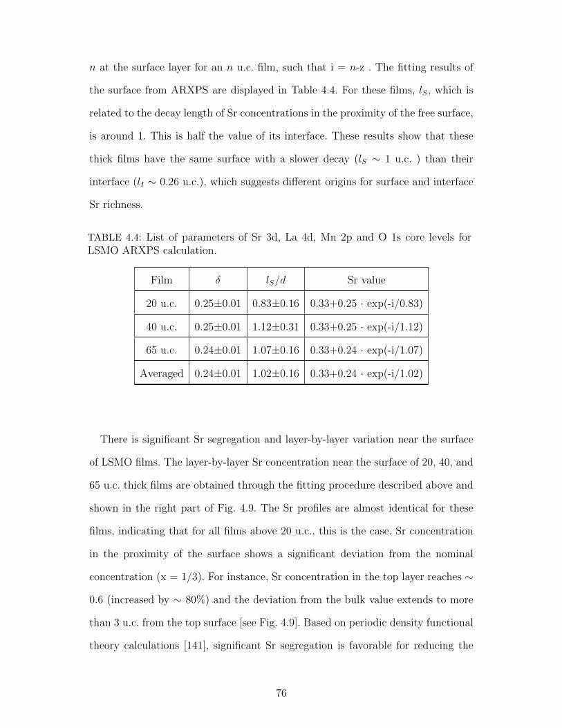
n at the surface layer for an n u.c. film, such that i = n-z . The fitting results of
the surface from ARXPS are displayed in Table 4.4. For these films, lS, which is
related to the decay length of Sr concentrations in the proximity of the free surface,
is around 1. This is half the value of its interface. These results show that these
thick films have the same surface with a slower decay (lS ∼ 1 u.c. ) than their
interface (lI ∼ 0.26 u.c.), which suggests different origins for surface and interface
Sr richness.
TABLE 4.4: List of parameters of Sr 3d, La 4d, Mn 2p and O 1s core levels forLSMO ARXPS calculation.
Film δ lS/d Sr value
20 u.c. 0.25±0.01 0.83±0.16 0.33+0.25 · exp(-i/0.83)
40 u.c. 0.25±0.01 1.12±0.31 0.33+0.25 · exp(-i/1.12)
65 u.c. 0.24±0.01 1.07±0.16 0.33+0.24 · exp(-i/1.07)
Averaged 0.24±0.01 1.02±0.16 0.33+0.24 · exp(-i/1.02)
There is significant Sr segregation and layer-by-layer variation near the surface
of LSMO films. The layer-by-layer Sr concentration near the surface of 20, 40, and
65 u.c. thick films are obtained through the fitting procedure described above and
shown in the right part of Fig. 4.9. The Sr profiles are almost identical for these
films, indicating that for all films above 20 u.c., this is the case. Sr concentration
in the proximity of the surface shows a significant deviation from the nominal
concentration (x = 1/3). For instance, Sr concentration in the top layer reaches ∼
0.6 (increased by ∼ 80%) and the deviation from the bulk value extends to more
than 3 u.c. from the top surface [see Fig. 4.9]. Based on periodic density functional
theory calculations [141], significant Sr segregation is favorable for reducing the
76

total surface energy of these polar perovskite oxides films. This will be discussed
further in the next chapter.
FIGURE 4.8: (a) Intensity ratio of Sr3d to La4d cores as a function of the emissionangle θ for different thickness of LSMO films. (b) The experimental (20, 40 and65 u.c.) and fitted (65 u.c.) intensity ratios of Sr3d/La4d as a function of emissionangle for LSMO films.
However, the Sr concentration profile near the interface behaves differently. As
shown in the left side of Fig. 4.9, the Sr profiles for the ultrathin films (4 u.c.
and 8 u.c.) are different from that of the 40 u.c. film. The value lI = 0.26 u.c. is
related to the decay length for the 40 u.c. film and is only about 1/4 of that for
ultrathin films (lI = 0.96 u.c.) which is compatible with the lS = 1 u.c. near the
free surface. Because Sr compositions at the interface suffer from influence from its
surface for ultrathin films, Fig. 4.9 shows the Sr doping variation at the interface
that reflects the pure intrinsic interfacial effects only for thick samples such as the
40 u.c. film. The measured interface Sr profiles for ultrathin films should combine
both intrinsic interface and surface contributions. Therefore, compared with these
results near the surface, we can conclude that the deviation of the Sr concentration
at the interface is small (only 1 u.c.), while in the proximity of the surface it is
much larger (3 u.c.)[see Fig. 4.9]. The inter-diffusion may be the main reason for Sr
77
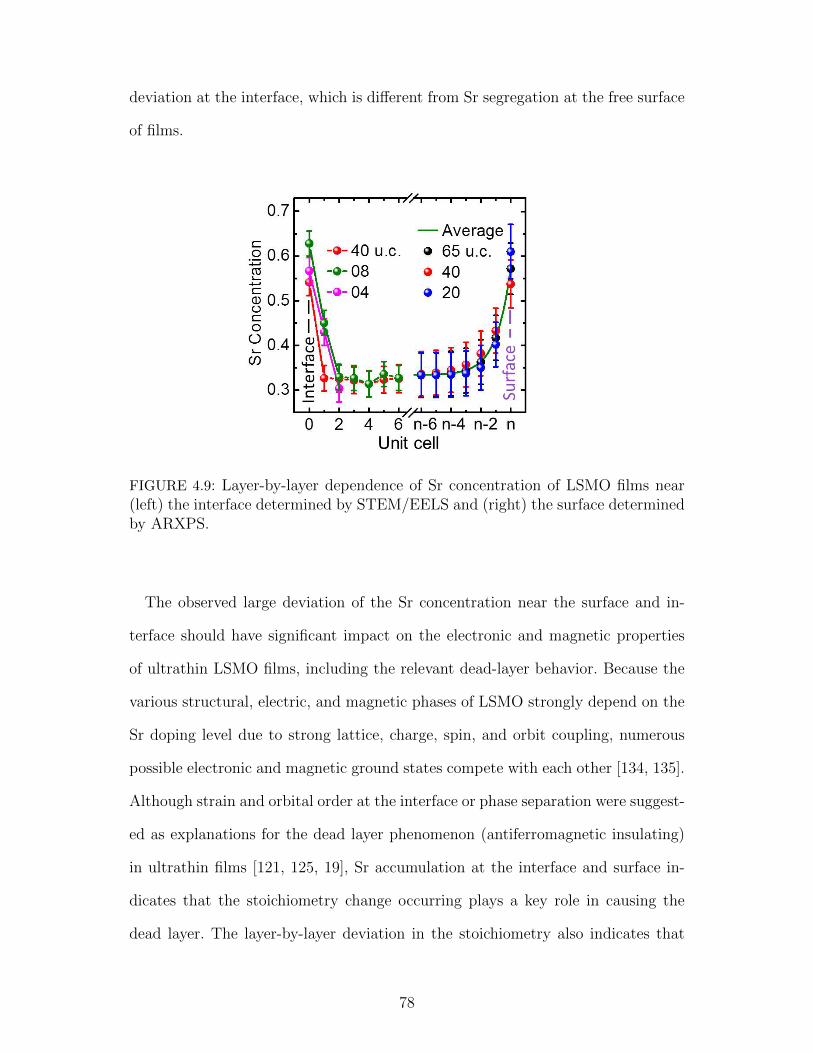
deviation at the interface, which is different from Sr segregation at the free surface
of films.
FIGURE 4.9: Layer-by-layer dependence of Sr concentration of LSMO films near(left) the interface determined by STEM/EELS and (right) the surface determinedby ARXPS.
The observed large deviation of the Sr concentration near the surface and in-
terface should have significant impact on the electronic and magnetic properties
of ultrathin LSMO films, including the relevant dead-layer behavior. Because the
various structural, electric, and magnetic phases of LSMO strongly depend on the
Sr doping level due to strong lattice, charge, spin, and orbit coupling, numerous
possible electronic and magnetic ground states compete with each other [134, 135].
Although strain and orbital order at the interface or phase separation were suggest-
ed as explanations for the dead layer phenomenon (antiferromagnetic insulating)
in ultrathin films [121, 125, 19], Sr accumulation at the interface and surface in-
dicates that the stoichiometry change occurring plays a key role in causing the
dead layer. The layer-by-layer deviation in the stoichiometry also indicates that
78

a non-metallic surface always exists in thick films even though the ferromagnetic
metallicity is dominant in overall film properties.
FIGURE 4.10: Intensity ratio of Sr3d plus La4d to Mn2p cores as a function of theemission angle θ for different thicknesses of LSMO films.
ARXPS provides information not only on the layer-by-layer Sr doping profile,
but also surface termination. Figure 4.10 is the angle dependence of the intensity
ratio of the (La 4d + Sr 3d) cores and the Mn 2p core for LSMO films with different
thickness. The enhanced intensity around 18 deg. and 45 deg. is due to the elastic
forward scattering effect, which is used to analyze the crystal structure through
x-ray photoelectron diffraction [99]. For thick films (≥20 u.c.), the θ dependence
of (La 4d + Sr 3d)/Mn 2p intensity ratio curves collapse into almost a single
curve, where the increasing magnitude with θ indicates that their terminations
are dominated by the (La/Sr)O layer. For thin films (n<20 u.c.), (La 4d + Sr
3d)/Mn 2p is more complicated, due to the substrate contribution at small θ.
However, estimated from the limited electron mean free path, the top 2 u.c. provide
about 98% of the contribution to the value of (La 4d + Sr 3d)/Mn 2p at θ =
81. Therefore, the intensity ratio at large emission angle θ should be reasonable
79

to determine the surface termination. We realize that the Sr surface segregation
also affects the value of (La 4d + Sr 3d)/Mn 2p. However, we estimate that the
maximum contribution for the drop of (La 4d + Sr 3d)/Mn 2p with decreasing
thickness is only ∼ 13%, much smaller than the observed ∼ 50% [see Fig. 4.10 at θ
= 81], thus indicating the change of termination layer with reduced film thickness.
FIGURE 4.11: (a) Intensity ratio of La4d to Mn2p cores as a function of the emissionangle θ for different thickness of LSMO films. (b) Intensity ratio of La4d to Mn2pcore as a function of film thickness for θ = 0 and 81. The inset presents thedetermined fraction of surface La/Sr-O termination for different thickness of LSMOfilms.
To further quantitatively understand the thickness dependence on the surface
termination without influence from the STO substrate, we chose the La 4d/Mn 2p
intensity ratio instead of (La 4d+Sr 3d)/Mn 2p to perform the quantitative analy-
sis, which is shown in Fig. 4.11 (a). Figure 4.11 (b) is the film thickness dependence
of the La 4d/Mn 2p intensity ratio at 0 and 81. Based on the Sr concentration
obtained from the above EELS and ARXPS results, the La 4d/Mn 2p intensity
ratio vs. film thickness data can be fit using the classical XPS model [see Eq.
4.2 and 4.3] with a mixed termination ratio between (La/Sr)O and MnO2 layers,
as shown in Fig. 4.11 (b). The (La/Sr)O termination percentage as a function of
80

film thickness is also obtained and shown in the inset of Fig. 4.11 (b). From the
calculated and fitting results, one can easily find that the thinnest film (4 u.c.)
in our experiment has a mixed termination dominated by MnO2, and the frac-
tion of (La/Sr)O termination increases with the film thickness. Although MnO2
termination is expected from the preservation of perovskite stacking due to the
epitaxial growth on STO with TiO2 termination, LSMO films eventually evolve
to pure (La/Sr)O termination at thicknesses above ∼ 20 u.c., consistent with the
surface energy DFT results claiming that La1−xSrxO termination has less energy
cost and higher stability [141]. In addition, different surface terminations of LSMO
films also provide different electrostatic potential at the interface of the associated
heterostructures, and will induce further influence on the interfacial structures,
such as octahedral tilt angle, cation displacement and so on. These differences and
changes also have significant impact on the electric, magnetic, and ferroelectric
properties of those artificial heterostructures [143, 144].
4.4 Summary
In this chapter, we report our studies on the thickness dependence of the chemical
composition variation with atomic layer precision for La2/3Sr1/3MnO3 (LSMO) thin
films grown on STO (001) substrate with TiO2 termination. The measurements
were performed utilizing a combination of in − situ and ex − situ microscopy
and spectroscopy tools. Our results reveal that there is a substantial increase in
the Sr concentration from its bulk value x = 0.33 both at interface and in the
proximity of the film surface, though they have distinct origins. The deviation
at the interface with the STO (001) substrate is mainly due to single unit cell
intermixing, but the deviation in proximity to the film surface is because of surface
Sr segregation. Although STO (001) with TiO2 termination was used as a substrate,
LSMO film surfaces experience a gradually self-organized conversion from MnO2
81

to (La/Sr)O layer termination with increasing film thickness. Such layer-by-layer
variation in chemical composition and its dependence on film thickness will have a
significant impact on the physical properties of these epitaxial films and relevant
heterostructures.
82

Chapter 5Surface investigation
5.1 Introduction and motivation
Perovskite manganites have been extensively studied for more than half a century
due to their rich physics such as colossal magnetoresisitance, charge ordering, half-
metallicity, and phase separation, which are related to the close coupling among
the charge, lattice, orbital, and spin [134]. The rich phase diagram of one such
perovskite, La1−xSrxMnO3, is shown in Fig. 1.5. LSMO is of particular interest due
to its high Curie temperature TC (∼ 369 K in the bulk crystals), its distinction
as the most electrically itinerant material among the manganites [135], and the
possible technological application. For LSMO ultrathin films, the metallicity as well
as ferromagnetic ordering are greatly suppressed [27, 136] and is usually referred to
as having a dead layer, so that the film exhibits a metal-insulator transition (MIT)
with reducing film thickness. Understanding the nature of the MIT still remains
highly controversial even though understanding and controlling such behavior is
essential for the future of interface physics.
In the previous chapter, the chemical composition variation with atomic layer
precision for LSMO films was given, and the data therein suggests that Sr variations
on the surface and interface have an immense impact on the physical properties of
the epitaxial films and heterostructures. Although similar conclusions about the
immense impact on the LSMO application and properties have been suggested
by many groups [66, 69, 140, 141, 145], there is no study about the influence on
surface properties coming from the significant composition deviations.
83

5.2 Surface morphology and local tunneling conductivity(STS/STM)
Scanning tunnelling microscopy (STM) and spectroscopy (STS) provide us with
powerful in-situ tools to characterize the local surface morphology and electronic
states of materials on the nanoscale, and help us obtain the intrinsic surface infor-
mation, such as morphology and electrical properties, of surface states of LSMO
thin films with Sr-rich surfaces that were observed by STEM and ARXPS in chap-
ter 4.
FIGURE 5.1: The STM morphological surface images of (a) 12 u.c., (b) 40 u.c.and (c) 60 u.c. LSMO films on STO with TiO2 termination. The STM images areobtained at bias voltage V = 1.0 V, tunneling current setpoint Ip = 20 pA, and atroom temperature).
Achieving an atomically-flat surface for these thin films is essential in order
to understand the physics of these oxides surfaces with broken symmetry as well
as produce any oxides-based device applications or other heterostructure fabri-
cations. After the systematic studies given in chapter 3 on the optimization of
growth parameters and conditions for LSMO films such as substrate preparation,
growth temperature, Ar/O2 and O3 gas pressure, laser power and frequency etc.,
we obtained layer-by-layer growth of thin epitaxial LSMO films on STO with TiO2
termination, which has better transport and magnetic properties as well as an
atomically flat surface. As a reminder, in chapter 3, the 12 u.c and 20 u.c. LSMO
films on STO(001) had an atomically flat surface, metallic behavior, and high elec-
84

trical conductivity, which was proven through LEED, RHEED, and STM images
and the temperature dependence of the resistivity shown in Fig. 3.5, Fig. 3.6, and
Fig. 3.8 respectively.
To further prove that the surface is atomically flat, LSMO films with different
thicknesses were investigated systematically with in-situ STM morphological sur-
face images, as shown in Fig. 5.1. The scans were recorded with a bias voltage of
1 V and a tunneling current setpoint of 20 pA at room temperature, the size of
images being 250 × 250 nm2 for 12 u.c., 120 × 120 nm2 for 40 u.c. and 100 ×
100 nm2 for 60 u.c., respectively. In Fig. 5.1, one can easily see that the films have
atomically flat surfaces with a clear step (∼ 0.4 nm) induced by the STO sub-
strate. The terrace width depends on the cut angle of the substrate and substrate
treatment processes. Even for the same batch of substrates, the terrace width can
vary from 20 nm to 50 nm. For all the films, the flatness of each step is within 1
u.c. (∼ 0.4 nm) and are devoid of any land-type flat grains.
The atomically resolved layer-by-layer stoichiometry was obtained with ARX-
PS and STEM and discussed in chapter 4, revealing that there is a considerable
deviation in the Sr concentration (x ∼ 0.57) from its bulk (x =1/3) value both
at the interface and close to the film surface. Based on the complex electric phase
diagram of LSMO introduced in chapter 1, the slight variation in Sr doping is
expected to have a significant impact on its physical properties. Therefore, the
Sr-rich deviation of 40%∼ 80% in the proximity of the film surface (within 1-2
u.c.) should cause distinctly different physical properties at the surface compared
to layers inside the film. To precisely extract the intrinsic electronic state of the
surface from the adjacent metallic inside layers, scanning tunneling spectroscopy
(STS) was performed systematically on LSMO films with different thicknesses at
different temperatures. Our STS measurements were taken by Pt-Ir tips cleaned
85

with focused ion beams. In addition, tungsten tips were also used for comparative
experiments to asses any tip influence on the experiment’s results, which will be
discussed later. Before taking each STS data set, the stabilization of the system
was checked by setting a bias voltage to V = 0.5 V and tunneling current setpoint
to Ip = 50 pA. The STM feedback was then turned off to fix the distance be-
tween tip and sample, after which the tunneling current I versus the bias voltage
V between sample and tip were measured and recorded as I −V spectra. For each
sample, we randomly chose 10 ∼ 15 locations for performing I − V spectra, and
for each location, twenty I − V curves were recorded, half scanning from +0.5 V
to -0.5 V, and half scanning -0.5 V to +0.5 V.
FIGURE 5.2: The 200 I−V curves of 40 u.c. LSMO film are measured at 10 differentlocations at (a) room temperature (RT) and (b) low temperature (∼ 100K, LT)(Vb = 0.5 V, Isetpoint = 50 pA).
Figure 5.2 shows the I − V spectra of the 40 u.c. LSMO film obtained at room
temperature (RT) and low temperature (LT)∼ 100K at different locations. The
insets display zoom-in’s of the spectra near the zero current region. In Fig. 5.2 (a),
the RT I − V spectra starting with both positive (+0.5 V) and negative(-0.5 V)
voltage biases have similar gapless shapes, which suggests that the 40 u.c. LSMO
film is metallic at RT. In addition, the zoom-in spectra in the inset of Fig. 5.2 (a)
86

clearly shows that the voltage bias Vb = 0 V corresponds to a tunneling current of
It = 0 pA. Figure 5.2 (b) is the I −V spectra for the 40 u.c. LSMO film measured
at LT (∼ 100 K). Similar to the RT I −V spectra, there is no gap observed in the
LT I − V spectra. However, the zoom-in spectra in the inset of Fig.5.2 (b) clearly
shows that, when the tunneling current is It = 0, the applied voltage bias Vb is 95
mV rather than 0. This shift of voltage bias at zero tunneling current is completely
different from the STS I −V spectra for a normal metal. This shift of voltage bias
at zero tunneling current is called a ’zero current bias shift’ or ’bias shift’.
FIGURE 5.3: The differential tunneling conductance dI/dV spectra of 40 u.c.LSMO film measured at (a) room temperature (RT) and (b) low temperature(∼ 100K, LT) (Vb = 0.5 V, Isetpoint = 50 pA).
In our particular case, the bias shift also can be defined by the minimum of the
dI/dV spectra. In our experiments, the tunneling conductance dI/dV −V spectra
are directly measured by a lock-in amplifier. For samples with the same thickness,
the dI/dV − V curves measured at different locations at certain temperatures are
very similar. Each dI/dV −V spectrum reported here has an average of about 200
dI/dV − V curves measured at 10 different locations. Figure 5.3 is the averaged
dI/dV − V spectra of the 40 u.c. LSMO film at RT (a) and LT∼ 100K (b). The
minimum of dI/dV is marked with the red dash line. In Fig. 5.3, the minimum of
87

the tunneling conductance spectrum at RT is around Vb = 0 V, while the minimum
at LT ∼ 100 K is at a bias shift of - 0.1 ± 0.01 V, which is consistent with the
results obtained in the I − V spectra in Fig. 5.2.
FIGURE 5.4: (a) Bias shift of 40 u.c. LSMO film extracted from the STS spectrameasured by using Pt-Ir tip and W tip at RT and low temperature (LT∼ 100k).(b) The STS spectra of 10 u.c. SrVO3 film measured at low temperature (∼ 100k)(Vb = 0.5 V, Isetpoint = 50 pA (blue) and 100 pA(red))
Before we further discuss the underlying physics of the bias shift phenomenon,
any possible extrinsic disturbances needs to be ruled out, such as from tips or other
STM/STS instruments, or other uncertain factors. First, to figure out whether the
bias shift comes from the tips of the STM, we repeated the LT STS experiments
many times using different Pt-Ir tips, and these experiments always gave the same
bias shift value for the 40 u.c. LSMO films. Those results are not shown here.
Furthermore, we also used tungsten tips to explore different materials to repeat
the LT STS measurements on 40 u.c. LSMO films, the results of which are shown
in Fig. 5.4 (a). The results obtained by both the W tip and Pt-Ir tip show a similar
bias shift value of - 0.1 ± 0.01 V. Secondly, to further exclude possible instrument
interference, a standard sample of highly oriented pyrolytic graphite (HOPG) was
measured at LT, and the spectra of HOPG found were consistent with the results
88

reported by other groups. There was no bias shift observed for HOPG in the LT
STS spectra. We also grew a 10 u.c. SrVO3 (SVO) film on the TiO2 terminated
STO substrate, and it was observed that the SVO film has good conductivity and
shows a metallic behavior, much the same as LSMO. However, different from the
LSMO films, there was no element segregation or accumulation at the surface of
SVO because Sr is the only element at the A-site of these perovskites. For the SVO
film, I − V spectra were also measured at RT and LT∼ 100 K. The STS spectra
of our SVO film shows normal metallic STS spectra without any bias shift, seen
in Fig. 5.4(b). The above RT and LT STS experiments of HOPG and SVO films
were performed using the same STM/STS instrument as was used to investigate
the LSMO films. Therefore, we can safely conclude that the bias shift observed on
LT LSMO films is not due to extrinsic instrumentation issues.
FIGURE 5.5: (a) Schematic view of 8 u.c. LSMO film grown on STO substratecapped with 10 u.c. SVO films. (b) The dI/dV − V spectra of 8 u.c. LSMO filmand 8 u.c. LSMO film capped with 10 u.c. SVO obtained at RT and LT ∼ 100 K,respectively.
To further investigate the origin of the bias shift, the experiment is designed to
determine if the bias shift originates from the LSMO film surface or the interface
between LSMO films and the STO substrate. Only 8 u.c. LSMO thin films were
89

studied with the STS, and the dI/dV spectra at RT and LT are shown in Fig.
5.5 (b), which only shows a bias shift of Vshift = - 0.08 ± 0.01 V at LT, which is
comparable to the Vshift = - 0.1 ± 0.01 V from 40 u.c. LSMO films. In the SVO
experiment above, the STS spectra shows that SVO has the same conductivity as
LSMO and no bias shift at RT or LT [see Fig. 5.4 (b)]. To probe their relationship,
another 10 u.c. SVO film was grown on top of the 8 u.c. LSMO film, as illustrated
in Fig. 5.5 (a). The electronic properties of this LSMO/SVO bilayer film were s-
tudied using STS. As with previous research done by my group where LSMO thin
films were capped with STO, the 8 u.c. LSMO film with 10 u.c. SVO capping
should show a better conductivity and ferromagnetism with higher Tc than the 8
u.c. LSMO without capping. The original surface of the LSMO film is destroyed
however, changing into an interface between LSMO and SVO. The dI/dV − V
spectra of the LSMO film with 10 u.c. SVO capping shows a metallic characteri-
zation much the same as the metallic SVO film, and no bias shift is observed at
LT. The bias shift in the STS spectra should be observed at LT if the shift comes
from the interface between the LSMO film and STO substrate, because SVO cap-
ping only suppresses the surface of LSMO and has no impact on that interface.
This experiment further confirms that the bias shift behavior is most likely due to
the non-conductive LSMO surface state. These bias shift phenomena are typically
observed in insulating ferroelectric materials due to spontaneous electric polar-
ization [146, 147], the insulating surface of polar compounds due to electrostatic
coupling induced polar surfaces [130], or p-n junctions under illumination due to
the photovoltaic effect [148, 149, 150]. In general, these bias shift phenomena are
the result of the electric field based on the non-conductive grain boundary or sur-
face due to the external excitation-induced charge accumulation or spontaneous
electric polarization.
90

To further confirm the existence of an electric field (or charge accumulation)
at the surface of LSMO at low temperature, the LT XPS is performed on a 40
u.c. LSMO film. Figure 5.6 (a) shows the O 1s spectra of the 40 u.c. LSMO
film measured at RT and LT ∼ 100 K with emission angle θ = 0. For θ = 0,
XPS mainly carries more information from the inside of the LSMO films. The
asymmetric peak shape of O 1s, which comes from the low energy electron hole
excitation, indicates the internal metallicity of the LSMO film.
FIGURE 5.6: (a) XPS O 1s core-level spectra of 40 u.c. LSMO film on STO substratemeasured at RT and LT ∼ 100 K. (b) The binding energy difference for RT andLT La 4d, Sr 3d, Mn 2p and O 1s core-level spectra of 40 u.c. LSMO film.
Compared with the O 1s core at RT, O 1s at LT shifts to a higher binding
energy by about 0.1 eV. Similarly, the binding energy differences between RT
and LT for the Sr 3d, Mn 2p, and La 4d spectra individually are also compared,
as shown in Fig. 5.6(b). The XPS spectra are measured in 0.1 eV steps, so the
0.1 eV error bar is a given in our XPS data. In chapter 4, ARXPS and STEM
demonstrate the chemical composition variation with atomic layer precision for
the LSMO films and show that the top ∼ 2 u.c. layers of the LSMO films have
much larger Sr doping (0.45-0.56) than the inside layers(x = 1/3). Based on the
phase diagram of LSMO, the composition analysis also suggests that the top 2 u.c.
91

layer should show much less conductivity and might even become insulating. STS
also demonstrates that the surface is nonmetallic at LT. The 40 u.c. LSMO film
is very metallic, having excellent conductivity in the bulk. However, for the XPS
spectra, the binding energy of all elements (La, Sr, Mn, and O) obtained at LT are
higher than at RT, which is consistent with the STS results, and should be due
to surface charge accumulation and a surface induced electric field. We can then
safely conclude that the bias shift in the STS spectra and XPS spectra shift to
higher binding energy at low temperature, which directly demonstrates that the
surfaces of both thin and thick LSMO films are nonmetallic, which is distinct from
the inside metallic layers in thick LSMO films.
FIGURE 5.7: (a) Schematic view of the polar surface of thick LSMO film basedon the ARXPS results. The yellow arrow is the spontaneous polarization PS. (b)Schematic diagram of the STS experiment. I is the tunnel current, and V is thebias applied between the tip and sample.
Furthermore, the bias shift in our low temperature STS experiments also indicate
that a spontaneous electric field exists in the non-conductive Sr-rich surface. The
physical effects that induce this spontaneous electric field in the epitaxial growth
of polar LSMO thin films with non-conductive surfaces are still in question. It is
well known that the emergence of a two-dimensional electron gas in LAO/STO
92

comes from the so-called polar discontinuity, which was introduced in chapter 1 in
detail. The presence of this polar discontinuity at the interface leads high density
bound charges at the interface. These bound charges incite a linear divergence of
the electrostatic potential with increasing polar compound (LAO) thickness, a phe-
nomenon referred to as polar catastrophe. To avoid the potential divergence and
reduce the energy cost, the junction or surface undergoes charge redistribution to
screen these bound charges by the displacement of ions or electronic reconstruction,
thus creating a spontaneous electric polarization. The emergence of spontaneous
polarization has been theoretically predicted and experimentally observed in polar
and non-polar oxide heterojunctions. In the discussion of layer-by-layer composi-
tion in chapter 4, our ARXPS date not only calculates the concentration variation
at the surface of LSMO films, but also provides termination information for the
thick films. According to our ARXPS results, the schematic of the elemental stack-
ing and bound charge stacking in the non-conductive 2 u.c. top surface layers of
LSMO films are drawn in Fig. 5.7 (a). Although the total charge in each top layer
has some variation due to the Sr concentration change, these bound positive and
negative charge stacking induced spontaneous electric polarizations do not change
their directions because the same elemental stacking order and (La,Sr)O termina-
tions of LSMO thick films grown on STO with TiO2 termination are seen. Since
the electrostatic screening effect is from metallic layers below the top insulating
surface layers, the spontaneous electric polarization PS comes only from the con-
tribution of the several top surface layers of LSMO films (2-3 u.c.). Based on the
direction of PS marked with the yellow arrow in Fig. 5.7 (a), a positive electric
field E is generated in the top surface of LSMO films. To illustrate the influence of
a positive spontaneous electric polarization PS in the STS spectra, a schematic of
the STS experiment is given in Fig. 5.7 (b). In an STS experiment with sample bias
93

V and a grounded tip, by changing the external bias voltage VE, the corresponding
tunneling current It is measured. As shown in Fig. 5.7(b), when the positive bias
is applied to the sample, the positive tunneling current It is measurable and in
the clockwise direction. If the LSMO film has a positive spontaneous potential VS
built into the surface, the total bias voltage Vt between the tip and the sample is
given by VE + VS. If VE = 0, the positive tunneling current It can still be excited
by a spontaneous VS. If zero current is desired, then Vt must equal 0 (VE = - VS),
which causes a negative bias shift in the STS spectra. Currently, this argument is
based on the ARXPS results without any structural distortion, and its influence
will be discussed later.
FIGURE 5.8: (a) Averaged and tunnel spectra of the 4, 6, and 8 u.c. LSMO filmsat LT ∼ 100 K. (b) The thickness dependence of bias shift obtained at RT and LT∼ 100 K.
We further investigate the thickness dependence of the bias shift. The films
with thicknesses ranging from 4 u.c. to 40 u.c. are all grown on STO with TiO2
termination under the same growth conditions. Figure 5.8 (a) is the dI/dV spectra
of 4, 6, and 8 u.c. LSMO films measured at LT ∼ 100 K. One can easily observe that
the 4 u.c LSMO film has a clear gap in its tunneling conductance spectra, consistent
with the insulating behavior of the 4 u.c. LSMO film observed with standard
94

electrical transport measurements. If we assume the exiting gap is symmetric about
the fermi level, the bias shift of 4 u.c. LSMO is around 0.15 V. Although the
temperature dependence of the resistance of the 6 u.c. film displays insulating
behavior, it does not show a clear gap in the LT STS spectra, which suggests that
the metallic layer still exists at LT. Since the films grow layer-by-layer on STO
substrates in many steps of 20-100 nm width and 0.4 nm height (see Fig.5.1),
the insulating behavior observed in the macroscale resistance measured using the
standard four-probe method is the result of these step induced-grain boundaries
and the insulation of the conductive layers in such thin films (only 2.4 nm) from
each other. However, the STS spectra, which only reflect local information, show a
nanoscale electronic state for the films. For 8 u.c. LSMO films, the dI/dV spectrum
is similar to that of 40 u.c. thick films. To investigate the evolution of the bias shift
with the thickness of films, the dependence of bias shifts on thickness n in u.c. are
given in Fig. 5.8 (b). At RT, I −V spectra for all films do not show any bias shift.
While at a LT of about 100 K, the bias shift value is around 90 mV for all films
except the 4 and 6 u.c. films. This indicates that the films above 8 u.c. have the
same surface states which are non-conductive with SrO termination and Sr-rich
due to the Sr segregation at the surface, which is consistent with the elemental
composition analysis results obtained from our ARXPS and STEM. For ultrathin
4 and 6 u.c. films, the bias shift is almost double the value of the thick films due to
these ultrathin films showing insulating behavior not having electrostatic screening
influences.
The temperature evolution of the bias shift for 40 u.c. LSMO film was also
investigated with the temperature range from 100 K to 300 K. Based on the I−V
and dI/dV spectra, the bias shift as a function of temperature is obtained and
shown in Fig. 5.9, where the black spots represent the bias shift without light
95
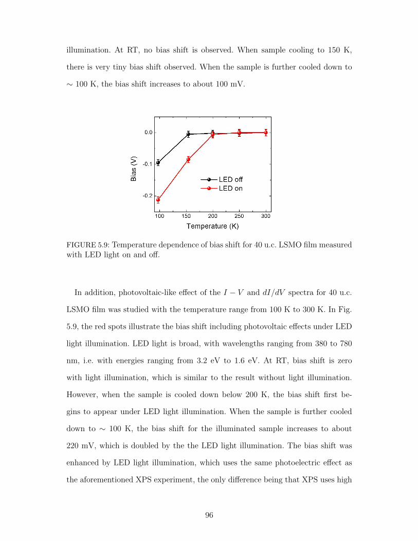
illumination. At RT, no bias shift is observed. When sample cooling to 150 K,
there is very tiny bias shift observed. When the sample is further cooled down to
∼ 100 K, the bias shift increases to about 100 mV.
FIGURE 5.9: Temperature dependence of bias shift for 40 u.c. LSMO film measuredwith LED light on and off.
In addition, photovoltaic-like effect of the I − V and dI/dV spectra for 40 u.c.
LSMO film was studied with the temperature range from 100 K to 300 K. In Fig.
5.9, the red spots illustrate the bias shift including photovoltaic effects under LED
light illumination. LED light is broad, with wavelengths ranging from 380 to 780
nm, i.e. with energies ranging from 3.2 eV to 1.6 eV. At RT, bias shift is zero
with light illumination, which is similar to the result without light illumination.
However, when the sample is cooled down below 200 K, the bias shift first be-
gins to appear under LED light illumination. When the sample is further cooled
down to ∼ 100 K, the bias shift for the illuminated sample increases to about
220 mV, which is doubled by the the LED light illumination. The bias shift was
enhanced by LED light illumination, which uses the same photoelectric effect as
the aforementioned XPS experiment, the only difference being that XPS uses high
96

energy X-ray and LED uses low energy visible light to excite electrons out of the
LSMO film. There are many experiments in perovskite ferroelectric oxides that
have observed photovoltaic efficiencies comparable to semiconductor p-n junction
solar cells [148, 149, 150]. Recently, intensive studies are focusing on how to use
the spontaneous polarization of ferroelectric oxides to enhance power conversion
efficiency in photovoltaic systems [149]. Our LED light enhancement of the bias
shift in the STS spectra suggests that high efficiency may be achieved in single
ferromagnetic perovskite oxides with a metallic bulk and spontaneous polarization
surface or interface due to elemental surface segregation and interface engineering.
5.3 Layer-by-layer structure
FIGURE 5.10: Comparison between experimental and theoretically-generated I(V)curves for the final structure of 2 u.c. LSMO film surface at RT
To quantitatively calculate and understand the origin of the bias shift, we further
used LEED-IV refinement to determine the surface structure and chemical com-
position. Nb-doped STO substrates were used for LEED experiments. The growth
conditions for the LSMO films for LEED I-V were similar to LSMO films used
in STM and XPS experiments. After films were grown in the growth chamber,
they were in − situ transferred into the main chamber for LEED analysis. The
LEED-IV was taken at room temperature at an ultra high vacuum pressure of 4
97

× 10−10 Torr. The surface structure is p(1×1), which has already been illustrated
in chapter 2.
FIGURE 5.11: (a) bulk structure of LSMO and (b) Surface Structure of 2 u.c.LSMO film
To determine details of the structure and their evolutions with thickness, LEED-
IV structural refinements were performed. Final LEED-IV refinement of a 2 u.c.
LSMO sample is shown in Fig. 5.10, which gives an extremely low Rp factor of
0.16. For the LEED-IV refinement, the Rp factor needs to be smaller than 0.3,
where lower Rp means the surface structure refinement is more reliable. Based on
the LEED IV refinement, the relative atomic postions of the surface are given in
Table 5.1 and the structure model is shown in Fig. 5.11.The LEED-IV refinement
shows that the topmost atomic layer is SrO. Because LEED is only sensitive to
the top layer, our assertion of an SrO layer on the surface is reliable. In the LEED
refinement, although the ratio of the Sr/La layer is given by La0.5Sr0.5, the insen-
sitivity of LEED to any other levels underneath the second (La/Sr)O layer makes
the exact La to Sr ratio at inner layers unclear. According to the refinement re-
sults, both Sr and O in the topmost layer move down. In particular, the Sr moves
98

down by 0.2952 A, while O moves down 0.0685 A. The atoms of MnO2 in the 2nd
layer are not in their original bulk positions. Mn moves down 0.0112 A , while two
O atoms move down about 0.0822. As a result, the out of plane lattice constant
in the (001) direction of the topmost unit cell is compressed by 0.27 A, and the
bottom unit cell is compressed by 0.09 A. The averaged lattice constant for a 2
u.c. LSMO sample is 3.7 A.
TABLE 5.1: Relative atomic positions of the refined surface structure of 2 u.c.LSMO film grown on STO.
Layer Atom Bulk position (A) Surface position (A) 4Z (A) Error (A)
1 Sr 0.0000 0.2952 +0.2952 ± 0.03
1 O 0.0000 0.0685 +0.0685 ± 0.03
2 O 1.9467 2.0289 +0.0822 ± 0.04
2 O 1.9467 2.0289 +0.0822 ± 0.04
2 Mn 1.9467 1.9579 +0.0112 ± 0.01
3 La/Sr 3.8933 3.9232 +0.0299 ± 0.04
3 O 3.8933 3.9232 +0.0415 ± 0.05
4 O 5.8400 5.9313 +0.0913 ± 0.12
4 O 5.8400 5.9313 +0.0913 ± 0.12
4 Mn 5.8400 5.8269 -0.0131 ± 0.01
5 La/Sr 7.7867 7.7279 -0.0588 ± 0.07
5 O 7.7867 7.7336 -0.0531 ± 0.27
Similar to the 2 u.c. LSMO film, surface structure refinement of 6, 8, and 10 u.c.
films can be achieved by LEED-IV refinement, as shown in Table 5.2. The Rp for 6
u.c. and 10 u.c. LSMO are 0.3125 and 0.3155 respectively, which are good enough
99

for complex oxide films. For the 6 u.c. LSMO film, the best model shows 70% of Sr
at the topmost layer, while for a 10 u.c. film, the topmost layer is given by 60% of
Sr in the fitting model. Another remarkable part of the structure is that, for the 6
u.c. LSMO, the topmost surface unit cell is compressed by 0.73 A, which is bigger
than that of the 2 u.c. (0.27 A) and 10 u.c. (0.41 A) films. The second unit cell
is compressed by 0.05 A, which is a little smaller than that of the 2 u.c. (0.09 A)
and 10 u.c. (0.09 A) films.
TABLE 5.2: Relative atomic positions of the refined surface structure of 6 u.c. and10 u.c. LSMO films.
Layer Atom Bulk position Surface position Surface position
(A) (6 u.c.) (A) (10 u.c.) (A)
1 Sr/La 0.0000 0.5836 0.4041
1 O 0.0000 0.1149 0.0955
2 O 1.9467 2.2120 2.2415
2 O 1.9467 2.2120 2.2415
2 Mn 1.9467 2.0472 2.0067
3 La/Sr 3.8933 3.9232 3.8835
3 O 3.8933 3.9050 3.9593
4 O 5.8400 5.8909 5.6348
4 O 5.8400 5.8909 5.6348
4 Mn 5.8400 5.7781 5.7984
5 La/Sr 7.7867 7.5902 7.6912
5 O 7.7867 7.7637 7.8046
100
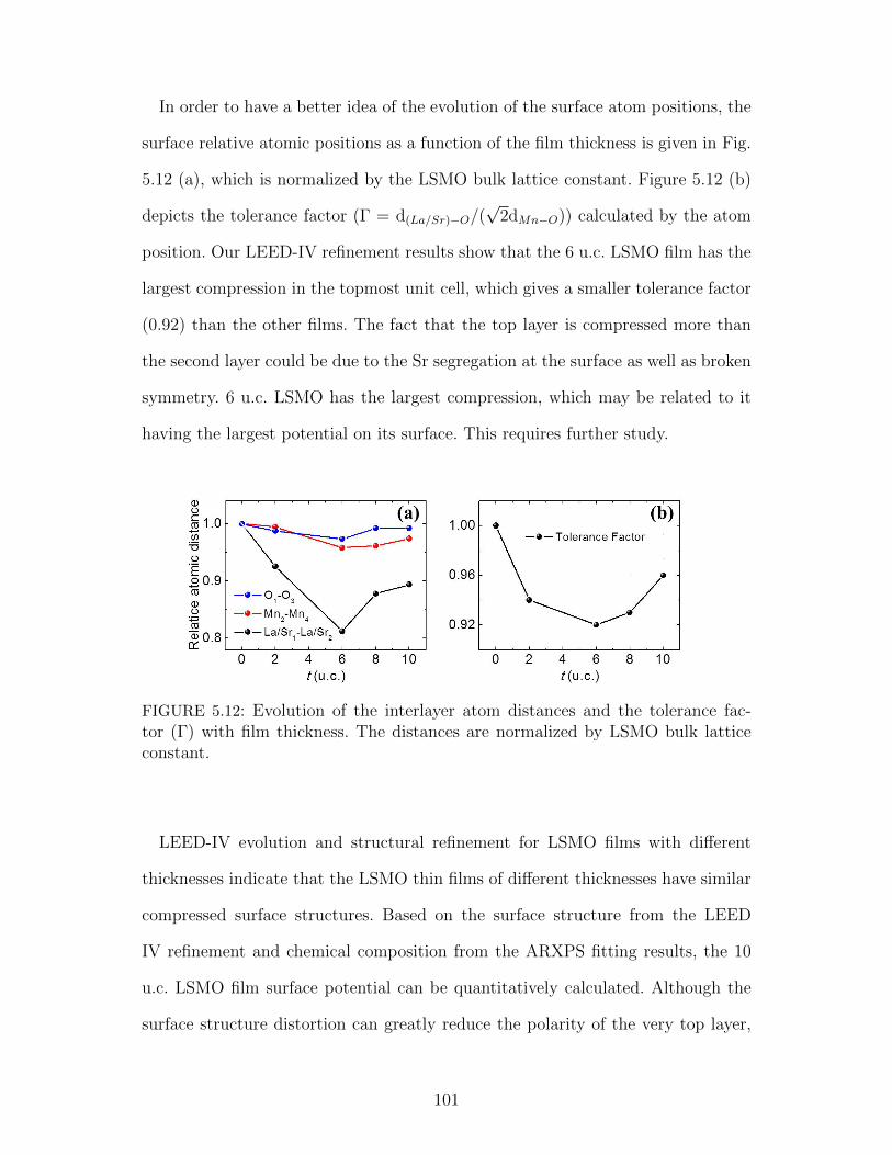
In order to have a better idea of the evolution of the surface atom positions, the
surface relative atomic positions as a function of the film thickness is given in Fig.
5.12 (a), which is normalized by the LSMO bulk lattice constant. Figure 5.12 (b)
depicts the tolerance factor (Γ = d(La/Sr)−O/(√
2dMn−O)) calculated by the atom
position. Our LEED-IV refinement results show that the 6 u.c. LSMO film has the
largest compression in the topmost unit cell, which gives a smaller tolerance factor
(0.92) than the other films. The fact that the top layer is compressed more than
the second layer could be due to the Sr segregation at the surface as well as broken
symmetry. 6 u.c. LSMO has the largest compression, which may be related to it
having the largest potential on its surface. This requires further study.
FIGURE 5.12: Evolution of the interlayer atom distances and the tolerance fac-tor (Γ) with film thickness. The distances are normalized by LSMO bulk latticeconstant.
LEED-IV evolution and structural refinement for LSMO films with different
thicknesses indicate that the LSMO thin films of different thicknesses have similar
compressed surface structures. Based on the surface structure from the LEED
IV refinement and chemical composition from the ARXPS fitting results, the 10
u.c. LSMO film surface potential can be quantitatively calculated. Although the
surface structure distortion can greatly reduce the polarity of the very top layer,
101

the calculation results show that the surface distortion only slightly reduces the
surface potential.
5.4 Film properties interpretation
Our data in chapter 4 shows that the segregation at the interface and surface is
roughly independent of LSMO film thickness. According to the layer-by-layer con-
centration of LSMO film achieved in chapter 4, we do believe that the substantial
increase in Sr concentration from its bulk value would result in nonmetallic be-
havior not only at the surface but also at the interface, which is illustrated in Fig.
5.13 (c). In a previous section of this chapter, the bias shift demonstrates that
the surfaces of LSMO films are none-metallic. Although we didn’t prove that the
interfaces of LSMO films are also none-metallic, we do believe that the interface
between LSMO and STO is also non-metallic.
To further study the influence of high Sr concentration to the properties of
LSMO films, the thickness dependence of the film conductivity is explained using
the model in Fig. 5.13 (c). Figure 5.13 (a) shows the temperature dependence
of the resistivity ρ of LSMO films with different thicknesses, which exhibits a
metal-insulator transition (MIT) with reduced film thickness. When film thickness
t ≤ 6 u.c., LSMO films are insulating, shown by the increase in resistivity as the
temperature decreases. When the t ≥ 7 u.c., LSMO films show metallic behavior.
For film thicknesses t ≤ 6 u.c., the resistivity is too high and cannot be measured.
With the measured resistivity results, the conductivities (σ) of the LSMO films
(≥ 7 u.c.) at 6 K as a function of film thickness are shown in Fig. 5.13 (b). The
thickness dependence of the conductivity shows that the conductivities of LSMO
films are not constant but rather gradually increase with increasing film thickness.
However, the thickness dependence of the conductivity can be modeled assuming
that there is a certain thickness (n0) of nonmetallic layers in a n u.c. LSMO film
102

such that only (n - n0) thick films are conductive. As shown in Fig. 5.13 (d), the
measured conductivity (σ) can be fitted to
σ = σreal · (n− n0)/n (5.1)
FIGURE 5.13: (a) Temperature dependence of the resitivity(ρ) of LSMO films withdifferent thicknesses. (b) Thickness dependence of the conductivity (σ) measuredat 6 K. (c) Schematic view of n u.c. LSMO film with a certain thickness (n0) ofnonmetallic layers near the surface and interface. (d) The thickness dependence ofthe measured conductivity (σ) times film thickness (n), measured at 6 K. The solidline is the fitting result with the suggested model by assuming a certain thickness(n0) of nonmetallic layers near the surface and interface of LSMO films on STO(001)
Here σreal is the constant real conductivity of the inside of the LSMO film. In
other words, σ · n =σreal *(n-n0) can be fit with a linearly dependent n. The fitting
result gives n0 = 6.5 and σreal = 7.68 (mΩ−1 · cm−1), which are comparable to the
103

measured critical thickness of the 6 u.c. film dead-layer and bulk conductivity (∼
11 mΩ−1 · cm−1) for LSMO single crystals [135], respectively.
The layer-by-layer concentration of LSMO films not only suggests the existence
of insulating layers, which had already been proven in this thesis, but also suggest-
s that antiferromagnetism exists near the surface and interface, which has been
seen by different groups. One such group used x-ray magnetic circular dichroism
to verify the existence of a canted antiferromagnetic insulating phase in ultrathin
LSMO films [151]. Another group used polarized neutron reflectometry to study
the exchange bias effects of LSMO grown on STO, which is related to the antifer-
romagnetic structure formed in this part of the LSMO thin film [152]. Although
the structural distortion needs to be considered in the antiferromagnetic insulating
phase of LSMO films and is the main focus of the above studies, the stoichiometry
change can have immense impact on LSMO films. The change of Sr doping can
not only turn metal to insulator, but can also change ferromagnetism to antiferro-
magnetism.
5.5 Summary
In this chapter, my study of the chemical composition of ultrathin films of LSMO
grown on STO (001) with atomic layer precision through a combination of in− and
ex − situ microscopy and spectroscopy techniques is detailed. Our results reveal
that there is a substantial increase in the Sr concentration from its bulk value both
at the interface and surface, which suggests that the surface and interface have
several nonmetallic layers. This should have an immense impact on the physical
properties of the epitaxial films and heterostructures.
To prove the existence of the insulating layer, STS was applied to LSMO films
with different thicknesses. For 4 u.c. LSMO, a gap is observed in the LT STS
spectra. For the LSMO films with thicknesses ≥ 6 u.c., the novel bias shift is
104

observed in the LT STS spectra, which cannot exist in the metallic layers but is
explained by the surface polarization due to Sr segregation. For 6 u.c. LSMO films,
the bias shift is about -0.24 V higher than other films (∼ -0.1 V). This is due to
the 6 u.c. LSMO film being more insulating and which may therefore accumulate
a higher potential between the interface and surface.
The surface structure of the LSMO films were studied with LEED, which demon-
strated that the 6 u.c. LSMO film has the largest compression in the topmost unit
cell, which gives a smaller tolerance factor (0.92) than the other film thicknesses.
This could be related to the 6 u.c. LSMO film having the largest polarization. Ac-
cording to the layer-by-layer concentration of LSMO films and the existence of the
persistent nonmetallic behavior near the surface of LSMO films, regardless their
thickness, the thickness dependence of conductivity is well explained by a model
that assumes a certain thickness (n0) of nonmetallic layers in an n u.c. LSMO film
such that only (n - n0) u.c.’s provide constant conductivity.
105

Chapter 6Introduce to the segregation theory andexperiment discussion in LSMO
6.1 Introduction and motivation
Segregation has been studied for over half a century, being predicted by McLean in
1957 [153]. It was first discovered at grain boundaries in metal alloys and has been
extensively studied due to the fact that the mechanical and chemical properties of
the alloys can be dramatically affected by the segregation. The grain boundary is
a defect of the crystal structure or the interface between two grains, or crystallites,
in a polycrystalline material. The existence of a grain boundary can decrease the
electrical and thermal conductivity of the material. A schematic illustration and
image of a low angle grain boundary is shown in Fig. 6.1. Compared to the bulk
crystal, grain boundaries usually have a higher Gibbs energy (grain boundary en-
ergy σ). Systems containing grain boundaries will tend to reduce this energy in
many ways. One way for a system to reduce its total energy is in the interaction of
the grain boundaries with other lattice defects such as solute or impurity atoms.
As a consequence, these atoms accumulate (segregate) at grain boundaries to some
extent. Once segregation appears, the chemical nature of the boundary becomes
qualitatively different from the inside of the bulk.
Segregation has important effects on the overall properties of a material. For
the metal alloys, segregation usually produces a deleterious effect on the quality,
which can lead to grain boundary fracture as a result of temper brittleness, creep
embrittlement, stress relief cracking of welds, hydrogen embrittlement, environmen-
tally assisted fatigue, grain boundary corrosion, and some kinds of intergranular
stress corrosion cracking [162]. Grain boundary segregation is a very important
phenomenon, which not only has an effect on the metallic properties, but also has
106

an important impact on other polycrystalline material properties. For example, it
may promote successful sintering of ceramic powders, and it also can dramatically
reduce the electric conductivity of semiconductors and high-temperature super-
conductors [168, 169, 170, 171]. Grain boundary segregation in metal alloys have
been deeply studied. Before moving on to discussing segregation in complex oxides
material, the grain boundary segregation of metal alloys will be briefly introduced
in the first part of this chapter.
FIGURE 6.1: Structure of a low-angle grain boundary (a) schematic illustration;(b) image of a [100] low-angle grain boundary in molybdenum revealed by thehigh-resolution electron microscopy. [172]
There are two recognized types of segregation: equilibrium segregation and non-
equilibrium segregation. To minimize the free energy in the segregation, one pos-
sible solution is the diffusion of elements from the bulk to the free surface, grain
boundary, and interface, which is called equilibrium segregation. Non-equilibrium
segregation was first theorized by Westbrook in 1964 [164]. Different from equilib-
rium segregation related to the minimization of the free energy, non-equilibrium
segregation occurs as a result of the solutes coupling to vacancies during quenching
107

or the application of stress, and can also be due to solute accumulation at a moving
interface [165]. Due to the different mechanisms, there is a distinguishable differ-
ence between non-equilibrium and equilibrium segregation. In the non-equilibrium
case, the lowest energy state corresponds to a uniform solute distribution. As a
result, the non-equilibrium segregation, which increases with increasing tempera-
ture, can be avoided by suitably heating the material to some temperature without
further quenching. In contrast, the lowest energy state in a system naturally ex-
hibits equilibrium segregation, and the extent of the segregation effect decreases
with increasing temperature [154]. Although vacancies can be caused by quenching,
component vacancies of a material, such as oxygen vacancies, are still included in
the later equilibrium calculation. In this chapter, we mainly focus on equilibrium
segregation.
Besides the segregation, there are two more important phenomena (phase sep-
aration and adsorption) for non-uniformity in the chemical composition of many
materials, namely those of phase separation and adsorption. The difference can be
clearly distinguished by the schematic diagrams of the three phenomena shown in
Fig. 6.2. Adsorption describes the attraction and retention of the molecules of a
substance on the surface of a liquid or solid resulting in a higher concentration of
molecules on the surface shown in Fig. 6.2(a), which can influence the results of
surface segregation experiments. Different from adsorption, phase separation and
segregation are inhomogeneous for the material itself shown in Fig. 6.2 (b) and
(c). Phase separation includes competing phases creating inhomogeneities in the
bulk. However, the segregation enriches the chemical material constituents at a free
surface or interface in a crystalline solid (including the crystalline films), as shown
in Fig. 6.3 (a). In a polycrystalline solid, a segregation site can be a dislocation,
108

grain boundary, stacking fault, interface with a precipitate, or a secondary phase
within the solid, shown in Fig. 6.3 (b).
FIGURE 6.2: The schematic diagrams for (a) absorption, (b) phase separation, and(c) segregation.
FIGURE 6.3: (a) Schematics of interface and surface segregation for a crystallinefilm; (b) Schematics of grain boundary segregation in a polycrstalline solid.
No grain boundary is observed with STEM in our LSMO films. Segregation to
free surfaces and interfaces is therefore the main phenomena investigated in the
second part of this chapter, focusing on theoretical and experimental segregation
results in complex oxide materials and LSMO. For the transition metal oxides,
segregation can be crucial to many properties, such as the overall device perfor-
mance in a range of device applications, including solid oxide fuel cells, oxygen
109
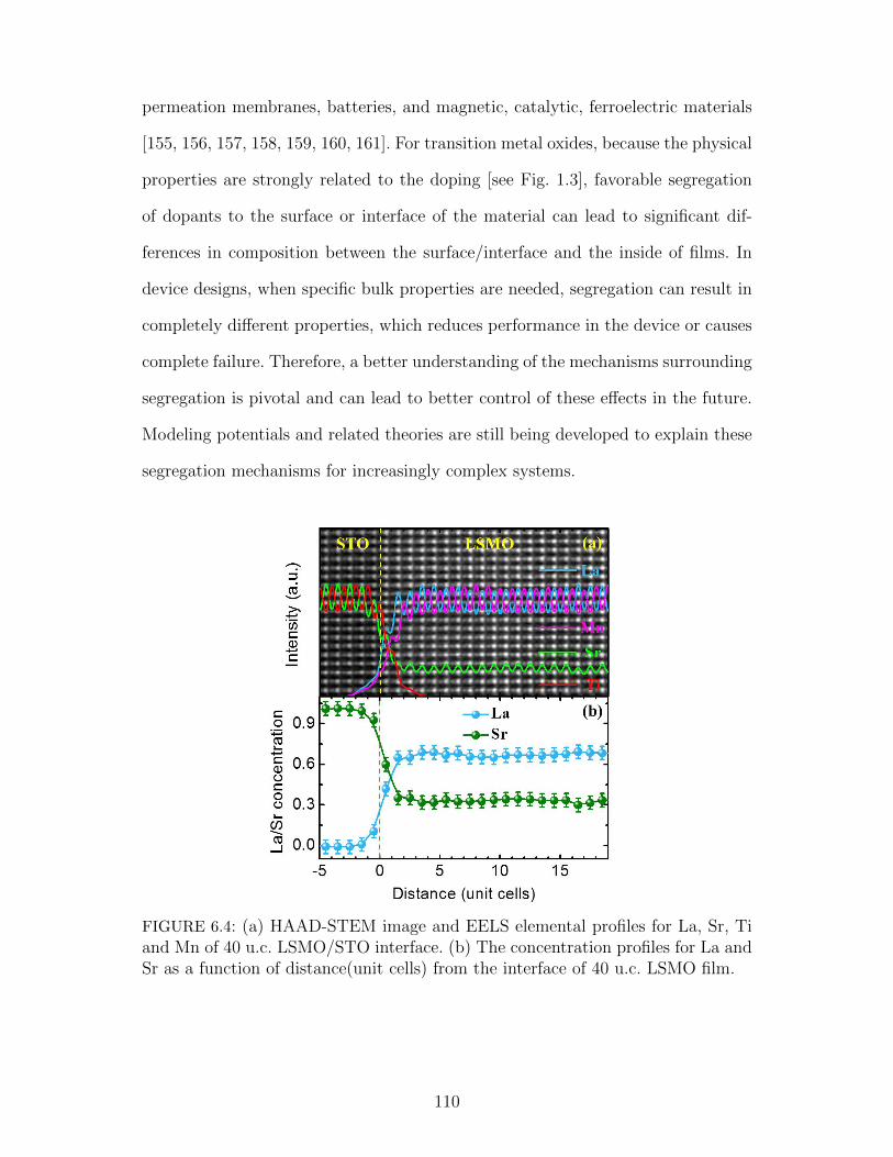
permeation membranes, batteries, and magnetic, catalytic, ferroelectric materials
[155, 156, 157, 158, 159, 160, 161]. For transition metal oxides, because the physical
properties are strongly related to the doping [see Fig. 1.3], favorable segregation
of dopants to the surface or interface of the material can lead to significant dif-
ferences in composition between the surface/interface and the inside of films. In
device designs, when specific bulk properties are needed, segregation can result in
completely different properties, which reduces performance in the device or causes
complete failure. Therefore, a better understanding of the mechanisms surrounding
segregation is pivotal and can lead to better control of these effects in the future.
Modeling potentials and related theories are still being developed to explain these
segregation mechanisms for increasingly complex systems.
FIGURE 6.4: (a) HAAD-STEM image and EELS elemental profiles for La, Sr, Tiand Mn of 40 u.c. LSMO/STO interface. (b) The concentration profiles for La andSr as a function of distance(unit cells) from the interface of 40 u.c. LSMO film.
110

6.2 Segregation in Metal alloys
Metallic materials have been used by mankind for eight millennia [166] and are still
irreplaceable in many applications to this day. Though we have used them for much
of our history, there is still ongoing research into understanding the mechanisms of
the processes at every stage of the production and application of metals. The first
attempts to describe segregation processes systematically were done by Agricola
[167]. His reports can be regarded as the first observations of phenomena induced
by grain boundary segregation.
6.2.1 Experimental Methods for Study of Grain BoundarySegregation
Grain boundary segregation has been detected by various methods both indirect-
ly and qualitatively. These techniques include many experimental measurements,
such as the electrode potential on grain boundary fractured surfaces, the variations
of lattice parameter with varied grain size using X-rays, spectrographic analysis
of material extracted from the grain boundary region, and so on [173]. However,
the limitations of these measurement techniques mean that they cannot be used
to fundamentally understand the grain boundary segregation. They are also not
applicable to ternary or more complex systems, where the effects of individual ele-
ments may overlap. To study segregation in a quantitative way, the techniques used
must satisfy two requirements, that they are suitable for the study of interfacial
composition that enables a direct approach to the interface as well as localization of
the analysis, and must also be able to give atomic resolution in at least one dimen-
sion. Therefore, there are typically two microscopic techniques used in the study of
grain boundary segregation, that of analytical electron microscopy (AEM), which
includes STEM, EELS and energy dispersive X-ray analysis (EDX) [174, 175, 176],
and atom-probe field ion microscopy (AP FIM), which can achieve atomic spatial
111

resolution with a mass spectrometer [177]. In our previous experiment results, the
interface segregation was studied by the STEM and EELS. Figure 6.4 is an ex-
ample of this, where the interface segregation can be shown in (b) obtained from
STEM and EELS results in (a).
6.2.2 Theoretical Study of Grain Boundary Segregation
As mentioned in the previous section, the appearance of equilibrium segregation
is a result of inhomogeneities in the solid giving rise to sites for which solute
atoms have a lower Gibbs energy. McLean was the first to develop a model to deal
explicitly with the phenomenon of grain boundary segregation. Since then, there
has been a steady effort to develop or improve the analytical models. Many groups
still try to give better predictions or interpretations of interfacial segregation.
Theories of equilibrium segregation can be developed with two different ap-
proaches. One approach is a quantum method studying the system on the mi-
croscopic level. This approach deals with interactions between segregating species
and the interface, as well as among the segregating species themselves. The other
approach deals with the thermodynamics of the system, which provides useful in-
terrelationships between the observable properties of the system in a macroscopic
way.
For the microscopic approach, one can attempt to directly solve the Schrodinger
equation. During the calculations, suitable approximations and processes are need-
ed. For example, density functional theory (DFT) is well developed and is a typi-
cal method used. In 1965, modern DFT was developed with Kohn-Sham equations
[197]. Later Walter Kohn was awarded the Nobel prize in chemistry for his develop-
ment of the density functional theory. However, DFT was not considered accurate
enough for calculations in quantum chemistry. In the 1990s, some approximations
(such as generalized gradient approximation) used in the DFT calculation, which
112

greatly help DFT to be a better model with the exchange and correlation interac-
tions [198].
The other way to approach the microscopics is with Molecular Mechanics based
on the interatomic potentials further calculated by computer simulation methods,
such as Molecular (or lattice) Statics, Molecular Dynamics, or Monte Carlo. These
computational potentials are much more efficient than first principle techniques
rooted in quantum mechanics, and enable simulations of systems that are several
orders of magnitude larger both with respect to length and time scales. Previous
attempts to develop a quantitative, microscopic theory have not been particularly
successful. The first numerically derived surface segregation energies which appear
quantitatively reasonable have been obtained by Foiles et al. [199]. The phase
field method has recently emerged as a powerful computational approach to solve
interface problems in materials at the mesoscale level. Phase field models were first
introduced by Fix [200] and Langer [201], which is a phenomenological phase field
model. Later, another phase field model was derived by Chen [202] and Wang [203]
from Khachaturyan’s microscopic theory [204, 205].
Segregation calculations also can be achieved by using thermodynamic models.
Compared with the quantum models, these statistical thermodynamic calculations
are simpler, but some have been applied to segregation with considerable success.
Based on the model built by McLean, many efforts have made done to thermody-
namic models, because of the simplicity it provides in the definitions of the relevant
model parameters. Besides, the simplicity of these thermodynamic models help us
to understand the driving forces for segregation more easily provides in the defini-
tions of the relevant model parameters. Based on the model built by McLean, the
majority of these efforts have made use of the regular solution approximation, be-
cause of the simplicity it. Therefore, in the following part of this section, we give a
113

brief introduction to the thermodynamic approaches, though detailed explanations
of the calculations only are explained in the original references.
The first and one of the simplest segregation models was built by McLean [153].
In binary metallic systems, by partitioning the solute atoms between lattice sites
and a fixed number of noninteracting grain-boundary sites, the energy of the system
can be minimized, which gives
χgχog − χg
=χb
1− χbexp(−∆G/KT ) (6.1)
Here, χg is the solute mole fraction at the grain boundary; χb is the solute mole
fractions in the bulk; χog is the saturation value for χg; ∆G is the free energy of
segregation; k is Boltz-mann’s constant; and T is the temperature of the system.
∆G can be estimated by Seah and Handros’s work [182], which extends the
theory of Brunauer et al [183].
∆G = ∆G′ + ∆Gs (6.2)
Here, ∆Gs is the free energy of precipitation for the soluble substances, which is
given by:
∆Gs = RTlnχob (6.3)
∆G′, the free energy for segregation without precipitation, is given by:
χgχog − χg
=χbχobexp(−∆G′/KT ) (6.4)
where χob is the solute solubility.
In the previous model, only the elastic energy contribution was considered. The
interactions between segregating species were first considered by Fowler in his
theory [184], where
χgχog − χg
= χbexp[−∆G− Z1W (χg/χ)og]/kT (6.5)
114

Here, W is the interaction energy and Z1 is the coordination number for the ad-
sorbate in the grain boundary layer. Further developments of Fowler’s theory were
done by Guttman [185]. In his work, he presented a theory to allow for interactions
between co-segregating species in ternary and higher-order systems, which further
modified the results:
χgiχogi
=χbiexp(−∆Gi/kT )
1 +∑
[exp(−∆Gi/kT )− 1](6.6)
Here, χgi is the molar fraction for co-segregating species. When two segregating
species appear in one system χb1 and χb2, the free energies for their segregations
∆Gi can be given by:
∆G1 = ∆Go1 + τ12χg2
∆G2 = ∆Go2 + τ12χg1
(6.7)
where τ12 is an interaction coefficient and ∆Goi are the free energies of segregation
for the species. If the interaction energies (τij,) disappear (i.e. equal to zero), the
result here is the same as with McLean’s model.
Another important model was built by Defay and Prigogine [189]. Although
they neglect the elastic effects, this model was appropriate to represent segregation
behavior of liquid solutions. However, as was pointed out by Burton and Machlin,
neither the McLean nor the Defay models were able to give qualitatively correct
predictions of grain boundary segregation with binary solid alloys [190]. The reason
for this is that one of them only considers chemical contributions to the heat
of segregation, while the other ignores the elastic contributions. As a result, the
considerations of a combined model in which the chemical and elastic contributions
to the heat of segregation were first recognized by Wynblatt and Ku [186]. The
total free energy is given by:
∆G = ∆Gint + ∆Gbin + ∆Gε (6.8)
115

Each of these terms is given by:
∆Gint = (γ1 + γ2)S (6.9)
∆Gbin = ∆Gm/3χb1χb2 (6.10)
∆Gε = −24πK ′Gr1r2(r1 − r2)2/(4Gr1 + 3K ′r2) (6.11)
where γi is the interfacial energy; S is the interface area per atom; ∆Gm is the
free energy of mixing of the binary solution, K is the bulk modulus of the solute,
G is the shear modulus of the solvent, and rl and r2 are the effective radii of the
solvent and solute, respectively.
In this model, there are three principal contributions responsible for segregation
in solid metallic alloys. The chemical driving force includes three distinct contri-
butions, the ∆Gint being the interfacial energy which depends on the difference
between the surface/interfacial energies of the pure components (i.e., a surface
energy driving force), and the ∆Gbin as a binary interaction contribution which
depends on the regular solution constant (i.e., an interatomic interaction driving
force). The third driving force ∆Gε is the elastic strain energy, which was first
identified by McLean. For this term, the contribution is associated with the de-
gree of misfit of the solute in solution. In ideal solution case, the ∆Gbin and ∆Gε
contributions can vanish.
After that, there are several refinements and modifications of these models that
have been proposed. For example, Lee and Aaronson first addressed the effects of
interface structure and energy anisotropy [187, 188]. However, the major driving
forces for segregation in metal alloys do not change much because the phenomeno-
logical descriptions of equilibrium segregation is qualitatively the same for all types
of interfaces. The differences are rooted in the model values of equilibrium grain
116
boundary segregation particular to thethermodynamic parameters resulting from
different structural/bonding conditions for individual cases [178, 179]. Because the
results for those models are for the non-ideal case, the composition profile, or the
changing segregation concentration from the surface to the bulk, is not necessarily
limited to the surface. In other words, the segregation is not limited to the first
two layers but can penetrate deeper. This is true even if only the first nearest
neighbor interactions are included. For values of the parameters usually employed
in these calculations, segregation is typically negligible beyond the third or fourth
layer from the surface.
6.3 Present Results and Discussion for LSMO film
LSMO is one important group of the complex oxide materials. In the previous
experimental result of LSMO films in chapter 4, the segregation is already proved
to be existing on the surface and at the interface. Interfacial segregation for these
systems describes the compositional heterogeneity that exists between the bulk
and interface due to interfacial effects that are distinct from the bulk. Alternative-
ly, surface segregation is the enrichment at the surface as a result of diffusion of
elements from the bulk moving to the surface region. When thermodynamic equi-
librium is reached, minimization of the total free energy at a given temperature
may result in the segregation on the surface and interface. The amount of segre-
gation enrichment depends on the growth conditions such as temperature, oxygen
pressure.
The presence of inhomogeneity at the surface can be due to Sr diffusion from the
bulk or absorption other elements such as carbon from the ambient background.
The adsorption can strongly influence the experimental study of the surface e-
quilibrium segregation. To investigate the surface segregation, ultrahigh vacuum
(UHV) of at least 10−10 Torr is required to reduce the influence of adsorption. Sur-
117

face sensitive characterization probes usually include Auger electron spectroscopy
(AES) and photoelectron spectroscopies (XPS, UPS, and ESCA). In chapter 4, the
surface segregation of LSMO films was analyzed by ARXPS.
6.3.1 Segregation driving forces in LSMO films
Because of differences in the nature of ceramics and metals, segregation theories for
metals cannot be directly extended to the case of ceramics [191]. The ionic nature of
ceramic oxides leads to the formation of electrostatic potentials at interfaces related
to the defects and structure, and there is no analogy in metals. Furthermore, doping
with an aliovalent ion in the complex oxides leads to a higher heat of solution in
ceramics than for that of metals. The heat of solution in ceramics is mostly related
to vacancy formation rather than the strain energy which is important in the case
of metals. Also, deviations from normal stoichiometry give rise to temperature
and oxygen partial pressure dependent variations in composition. Doping in these
manners with ceramics can produce a whole range of new variables, which do not
exist metallic alloys. Thus, electrostatic contributions need be considered in the
theory of interfacial segregation in complex oxides, such as perovskites.
Frenkel first pointed out that the existence of space charge regions at interfaces in
ionic solids lead to several nanometers of compositional heterogeneities extending
further into the materials [192]. Frenkel’s initial model and subsequent refinements
were further improved by Kliewer and Koehler [195]. All these methods have ap-
proached the problem by considering the space charge effect as the only major
driving force for segregation. Yan et al. [193, 194] further extended Kliewer and
Koehler’s approach by including additional elastic and dipolar effects. All these
theories were applied to alkali halides under equilibrium conditions.
Based on the approach used by Frenkel, Desu and Payne developed a model for
equilibrium interfacial segregation in pure and doped perovskite materials [196].
118

The approach used regular solution approximations and considered space charge ef-
fects as the major driving force for segregation. For dopant segregation, elastic and
electrostatic driving forces were considered. Giving the right solution to the model
in the doped system requires fully considering the charge neutrality conditions and
the strain energy contribution. One interesting prediction of this model is that the
thickness of the space charge layer (i.e. the decay length of segregation) decreases
with the increase of growth temperature, which was proved by comparison of the
calculated values and experimental results in BaTiO3.
There are some segregation calculations directly for LSMO. Recently, Harrison
has hypothesized that the surface charging of LSMO has its origin in the segrega-
tion of Sr at the surface of LSMO [67]. On the (100) surface of LSMO films, with
a uniform distribution of Sr and La cations, the charge of per site in La1−xSrxO
planes is +e(1-x). Harrison constructed an electrostatic model of the interaction
of Sr with the charged surfaces of LSMO. With this model, the total electrostatic
surface energy can be calculated, which shows that this energy could be minimized
by depleting the La and increasing the Sr concentration at or near the surface
of LSMO. In this paper, he predicted an La concentration of 0.65(1 − 0.41n) or
0.65(1 − exp(−0.89)n), where the decay length quantitatively equals the surface
segregation of LSMO, as shown in Table 4.4. Although bulk LSMO is metallic,
this result would seem to give compelling evidence that the surface is nonmetallic,
which is also proved by our STS experimental results in chapter 5, and the electro-
static energy is a source of the segregation of the dopant at the surface of LSMO.
However, according to the Harrison model, the decay length is fixed, but this re-
sult is contradictory to the prediction made in Desu and Payne’s model, that the
decay length of the segregation decreases with increasing temperature. Another
119

weak point of this model is its failure to predict the amount of segregation, which
is due to it neglecting the elastic energy as another driving force.
The importance of elastic energy was fully emphasized by another segregation
calculation and experiment related to LSMO done by Yildiz et al. [69]. The den-
sity functional theory (DFT) calculation considers both the elastic energy and
electrostatic energy as the driving forces for the surface segregation, which sug-
gests that Sr segregation toward the surface can minimize the elastic energy due
to a mismatch of the dopant and host cation sizes. It aslo minimizes the electro-
static energy due to the interactions between the dopants and charged defects at
the surface and the space charge zone near the surface, in addition to the sur-
face polarity effects. They also experimentally study the elastic energy differences
by changing the radius of selected dopants (Ca, Sr, Ba) with respect to the host
cations (La, Sm) while maintaining the same charge in an LnMnO3 system. A
smaller size mismatch between the host and dopant cations was found to suppress
segregation effects. They also studied the oxygen pressure influence on the elastic
and electrostatic energy.
LSMO is a part of a complex family of materials which could be important in
future technological application. With Sr doping 0.33, LSMO bulk is the metallic
state. However, the elastic energy can be the initial driving force for the Sr segrega-
tion in LSMO films, which induces the nonmetallic property of LSMO film. While,
in the nonmetallic layers of LSMO films, the electrostatic energy can further en-
hance the segregation effect. For complex oxides, current models still cannot fully
solve the segregation problem. However, it is undeniable that both the elastic and
electrostatic interactions must be quantitatively taken into account for segregation
calculations in complex materials.
120

6.3.2 Surface segregation in LSMO films
In general, the phenomenological description of free surface segregation is similar
to that for interface segregation. In the aforementioned models, there is no distinct
difference for the basic driving forces between the surface and interface segrega-
tions. Those models, originally designed for interface segregation, usually can be
extended to use with surface segregation. The McLean model is a good example for
this. Although it was originally designed for the segregation at grain boundaries,
it can also be applicable to segregation at free surfaces [180, 181]. If the amount
of segregation at the surface (only the topmost layer) is 0, denoted in fractions of
a monolayer, then
θ/(1− θ) = χexp(−∆ESeg/kT ) (6.12)
For a binary alloy with two components A and B, 0 is the surface layer concen-
tration of component B. Here, χ = χbB/(1 − χbB), and χbA) and χbB) are the bulk
concentrations of A and B respectively. ∆Eseg is the system energy change when
an atom of type B originally in the bulk changes position with an A atom originally
at the surface. In this model, all sites are assumed to have the same environment.
A positive value of Eseg corresponds to the enrichment of A at the surface, and a
negative value for B enrichment.
In chapter 4, by comparing the surface and interface segregation, we already
concluded that the deviation of Sr concentration at the interface is small (only 1
u.c.), while in proximity to the free surface it is more severe (3 u.c.)[see Fig. 4.9].
In other words, there is a difference in the Sr segregation decay length between the
interface and the free surface of films. One possible reason for the difference is that
the interface is metallic, while the free surface is nonemetallic. As the results, there
fundamental difference between the driving forces for the interface and the surface.
121

Besides, the different structures, which has a larger distortion on surface as shown
in section 5.3, and the different chemical environments such as oxygen vacancy of
the surface and interface can further influence the segregation. Although similar
theories can be used to explain the surface and interface segregation, the distin-
guish difference of the structure and chemical composition between the surface and
interface can cause a segregation difference between the two zones.
6.4 Summary
In this chapter, the importance of segregation in many materials was discussed.
Grain boundary segregation was first investigated in metal alloy systems and has
been intensively studied. The experimental tools for probing the grain boundary
were also introduced in the beginning of the chapter. The theory for equilibrium
segregation was first developed by McLean, but it cannot provide qualitatively
correct predictions for the segregating components at binary solid alloy surfaces
due to only including the elastic contributions to the driving force. Thermodynamic
models were also discussed. In the later models, the major driven forces for the
grain boundary segregation in metal alloys were made to include both the elastic
strain energy as well as the chemical driving force (i.e. the interfacial energy and
the binary interaction).
Using the previous theory calculations, the models built for the interface can
usually be extended to understand the surface. Although the driving forces consid-
ered are the same, the formula needs to be modified. In our experimental results,
the decay lengths at the surface and interface are completely different. This may
be due to needing a different formula for the calculation or being able to include
different structures and vacancies between the surface and interface.
Though it is not important with metals, the segregation model in complex oxide
materials needs to consider the electrostatic energy as one of the important driving
122

forces. In the early days of segregation studies, Frenkel pointed out the importance
of space charge regions at interfaces in ionic solids. Yan et al. extended the model,
and built the first approach to including electrostatic, elastic, and dipolar effects,
which gave a more precise prediction for ceramic oxides materials. To address the
segregation in pure and doped perovskite materials, Desu and Payne developed a
model for equilibrium interfacial segregation, where elastic and electrostatic driving
forces were considered.
For segregation calculations in LSMO films, there are two important papers.
Harrison’s work only considered surface charging in the origin of the segregation
of Sr at the surface of LSMO. In this model, the decay length is qualitatively the
same as those seen in our experimental results. However, the decay length does not
change with the growth conditions, which contradicts with the predictions of Desu
and Payne’s model. Without considering elastic energy, Harrison’s model cannot
predict the change of dopants in the segregation. Another important segregation
calculation and experiment related to LSMO was done by Yildiz et al.. The im-
portance of elastic energy was proven in their work by changing dopants in their
experiment. They used DFT calculations to further explain the experiment results,
which also consider the elastic and electrostatic energy as the major driving forces.
123

References
[1] https://en.wikipedia.org/wiki/Abundance of the chemical elements
[2] X. Wu, C. Zhang, P. Goldberg, D. Cohen, Y. Pan, T. Arpin, and O. Bar-Yosef,Science 336, 1696 (2012).
[3] J. G. Bednorz, and K. A. Muller, Zeitschrift fur Physik B 64, 189 (1986).
[4] C. W. Searle, and S. T. Wang, Can. J. Phys. 47, 2703 (1969).
[5] H. Schmid, Ferroelectrics 162, 317 (1994).
[6] M. A. Laguna-Bercero, Journal of Power Sources 203, 4 (2012).
[7] V. Anisimov, and Y. Izyumov, Electronic Structure of Strongly CorrelatedMaterials, Springer (2010).
[8] G. H. Jonker and J. H. Van Santen, Physica 16, 337 (1950).
[9] M. Imada, A. Fujimori, and Y. Tokura, Rev. Mod. Phys. 70, 1039 (1998).
[10] S. Jin, T. H. Tiefel, M. McCormack, R. A. Fastnacht, R. Ramesh and L. H.Chen, Science 264, 413 (1994).
[11] M. N. Baibich, J. M. Broto, A. Fert, F. Nguyen Van Dau, F. Petroff, P.Etienne, G. Creuzet, A. Friederich, and J. Chazelas Phys. Rev. Lett. 61, 2472(1988).
[12] G. Binasch, P. Grunberg, F. Saurenbach, and W. Zinn, Phys. Rev. B 39, 4828(1989).
[13] The Nobel Prize in Physics 2007, NobelPrize.org.
[14] J. -H. Park, E. Vescovo, H. -J. Kim, C. Kwon, R. Ramesh and T. Venkatesan,Nature 392, 794 (1998).
[15] S. A. Wolf, D. D. Awschalom, R. A. Buhrman, J. M. Daughton, S. von Molnr,M. L. Roukes, A. Y. Chtchelkanova, D. M. Treger, Science 294, 1488 (2001).
[16] S. Okamoto and A. J. Millis, Nature 428, 630 (2004).
[17] C. N. R. Rao and A. K. Raychaudhuri, Colossal Magnetoresistance, ChargeOrdering and Related Properties of Manganese Oxides (Eds. C.N.R. Rao andB. Raveau), Singapore: World Scientific (1998).
[18] A. -M. Haghiri-Gosnet and J. -P. Renard, J. Phys. D: Appl. Phys.36, R127(2003).
124

[19] N. Nakagawa, H. Y. Hwang, and D. A. Muller, Nature Materials. 5, 204 (2006).
[20] P. Zubko, S. Gariglio, M. Gabay, P. Ghosez, and J-M Triscone, Annual Reviewof Condensed Matter Physics2, 141 (2011).
[21] V. M. Goldschmidt, Die Naturwissenschaften 21, 477 (1926).
[22] Handbook of magnetism and advanced magnetic materials: Spintronics andmagnetoelectronics, (Eds, Helmut Kronmuller, Stuart Parkin) John Wiley ℘Sons (2007).
[23] H. A. Jahn and E. Teller, Proc. R. Soc. London A,161, 220 (1937).
[24] H. Sawada, Y. Morikawa, K. Terakura, and N. Hamada, Phys. Rev. B 56,12154 (1997).
[25] Y. Tomioka and Y. Tokura, Phys. Rev. B 70, 014432(2004).
[26] J. Stahn, J. Chakhalian, Ch. Niedermayer, J. Hoppler, T. Gutberlet, J. Voigt,F. Treubel, H-U. Habermeier, G. Cristiani, B. Keimer, and C. Bernhard, Phys.Rev. B 71, 140509(R) (2005).
[27] M. Huijben, L. W. Martin, Y. -H. Chu, M. B. Holcomb, P. Yu, G. Rijnders,D. H. A. Blank, and R. Ramesh, Phys. Rev. B 78, 094413 (2008).
[28] J. B. Goodenough, Phys. Rev.100, 564 (1955)
[29] C. Zener, Phys. Rev.81, 440 (1951)
[30] P. W. Anderson, and H. Hasegawa, Phys. Rev.100, 675 (1955)
[31] P. G. de Gennes , Phys. Rev.118, 141 (1960)
[32] A. Ohtomo and H. Y. Hwang, Nature 427, 423 (2004).
[33] S. Thiel, G. Hammer, A. Schmehl, C. W. Schneider, and J. Mannhart, Science313, 1942 (2006).
[34] A. Brinkman, M. Huijben, M. van Zalk, J. Huijben, U. Zeitler, J. C. Maan,W. G. van der Wiel, G. Rijnders, D. H. A. Blank and H. Hilgenkamp, NatureMaterials 6, 493 (2007).
[35] M. Ben Shalom, C. W. Tai, Y. Lereah, M. Sachs, E. Levy, D. Rakhmilevitch,A. Palevski, and Y. Dagan, Phys. Rev. B 80, 140403(R) (2009).
[36] N. Reyren, S. Thiel, A.D. Caviglia, L. Fitting Kourkoutis, G. Hammerl, C.Richter, C.W. Schneider, T. Kopp, A.-S. Retschi, D. Jaccard, M. Gabay, D.A. Muller, J.-M. Triscone, J. Mannhart, Science 317, 1196 (2007).
125
[37] J. A. Bert, B. Kalisky, C. Bell, M. Kim, Y. Hikita, H. Y. Hwang and K. A.Moler, Nature Physics 7, 767 (2011).
[38] N. Kida, H. Yamada, H. Sato, T. Arima, M. Kawasaki, H. Akoh, and Y.Tokura, Phys. Rev. Lett. 99, 197404 (2007).
[39] A. Savoia, D. Paparo, P. Perna, Z. Ristic, M. Salluzzo, F. Miletto Granozio,U. Scotti di Uccio, C. Richter, S. Thiel, J. Mannhart, and L. Marrucci, Phys.Rev. B 80, 075110 (2009).
[40] B. R. K. Nanda and S. Satpathy, Phys. Rev. B 81, 224408 (2010).
[41] R. H. Liu, W. L. Lim, and S. Urazhdin, Phys. Rev. Lett. 110, 147601 (2013).
[42] J. Chakhalian, J. W. Freeland, A. J. Millis, C. Panagopoulos, and J. M.Rondinelli, Reviews of Modern Physics 86 1189 (2014).
[43] Y. Tokura and N. Nagaosa, Science 288, 462 (2000).
[44] A. Tebano, C. Aruta, S. Sanna, P. G. Medaglia, G. Balestrino, A. A. Sidorenko,R. De Renzi, G. Ghiringhelli, L. Braicovich, V. Bisogni, and N. B. Brookes,Phys. Rev. Lett. 100, 137401 (2008).
[45] B. Cui, C. Song, F. Li, G. Y. Wang, H. J. Mao, J. J. Peng, F. Zeng, and F.Pan, Scientific Reports 4 4206 (2014).
[46] N. M. Nemes, M. J. Calderon, J. I. Beltran, F. Y. Bruno, J. Garcıa-Barriocanal, Z. Sefrioui, C. Leon, M. Garcıa-Hernndez, M. C. Munoz, L. Brey,and J. Santamarıa, Adv. Mater. 26 7516 (2014).
[47] D. Preziosi, M. Alexe, D. Hesse, and M. Salluzzo, Phys. Rev. Lett. 115, 157401(2015).
[48] H. Doganay, I. P. Krug, J. Schubert, S. Cramm, D. M. Gottlob, F. Nickel andC. M. Schneider, Europhysics Letters 109 67007 (2015).
[49] R. K. Zheng, Y. Wang, H. L. W. Chan, C. L. Choy, and H. S. Luo Phys. Rev.B 75, 212102 (2007).
[50] J. Z. Sun, D. W. Abraham, R. A. Rao, and C. B. Eom, Appl. Phys. Lett. 74,3017 (1999).
[51] C. Aruta, G. Ghiringhelli, A. Tebano, N. G. Boggio, N. B. Brookes, P. G.Medaglia, and G. Balestrino, Phys. Rev. B 73, 235121 (2006).
[52] A. Tebano, C. Aruta, P. G. Medaglia, F. Tozzi, G. Balestrino, A. A. Sidorenko,G. Allodi, R. De Renzi, G. Ghiringhelli, C. Dallera, L. Braicovich, and N. B.Brookes, Phys. Rev. B 74, 245116 (2006).
126

[53] Y. Takamura, R. V. Chopdekar, E. Arenholz and Y. Suzuki, Appl. Phys. Lett.92, 162504 (2008).
[54] G. Colizzi, A. Filippetti, F. Cossu and V. Fiorentini, Phys. Rev. B 78, 235122(2008).
[55] C. Adamo, X. Ke, H. Q. Wang, H. L. Xin, T. Heeg, M. E. Hawley, W. Zander,J. Schubert, P. Schiffer, D. A. Muller, L. Maritato and D. G. Schlom, Appl.Phys. Lett. 95, 112504 (2009).
[56] D. Pesquera, G. Herranz, A. Barla, E. Pellegrin, F. Bondino, E. Magnano, F.Sanchez and J. Fontcuberta, Nature Communications 3, 1189 (2012).
[57] B. Cui, C. Song, G. Y. Wang, H. J. Mao, F. Zeng, and F. Pan, ScientificReports 3, 2542 (2013).
[58] F. Sandiumenge, J. Santiso, L. Balcells, Z. Konstantinovic, J. Roqueta, A.Pomar, J. P. Espinos, and B. Martınez, Physical Review Letters 110, 107206(2013).
[59] A. Vailionis, H. Boschker, Z. Liao, J. R. A. Smit, G. Rijnders, M. Huijben andG. Koster, Applied Physics Letters 105 131906 (2014).
[60] J. Heidler, C. Piamonteze, R. V. Chopdekar, M. A. Uribe-Laverde, A. Alberca,M. Buzzi, A. Uldry, B. Delley, C. Bernhard, and F. Nolting, Physical ReviewB 91 024406 (2015).
[61] F. Y. Bruno, J. Garcia-Barriocanal, M. Varela, N. M. Nemes, P. Thakur, J. C.Cezar, N. B. Brookes, A. Rivera-Calzada, M. Garcia-Hernandez, C. Leon, S.Okamoto, S. J. Pennycook, and J. Santamaria, Physical Review Letters 106147205 (2011).
[62] O. Shapoval, S. Huhn, J. Verbeeck, M. Jungbauer, A. Belenchuk, and V.Moshnyaga, Journal of Applied Physics 113 17C711 (2013).
[63] X. Yin, M. A. Majidi, X. Chi, P. Ren, L. You, N. Palina, X. Yu, C. Diao, D.Schmidt, B. Wang, P. Yang, M. B. H. Breese, J. Wang and A. Rusydi, NPGAsia Materials 7 e196 (2015).
[64] H. Boschker, M. Huijben, A. Vailionis, J. Verbeeck, S. van Aert, M. Luysberg,S. Bals, G. van Tendeloo, E. P. Houwman, G. Koster, D. H. A. Blank, G.Rijnders, Journal of Physics D-Applied Physics 44 205001 (2011).
[65] M. Huijben, Y. Liu, H. Boschker, V. Lauter, R. Egoavil, J. Verbeeck, S. G.E. te Velthuis, G. Rijnders and G. Koster, Adv. Mater. Interfaces 2, 1400416(2015).
[66] H. Dulli, P. A. Dowben, S. -H. Liou, and E. W. Plummer, Phys. Rev. B 62,R14629(R) (2000).
127

[67] W. A. Harrison, Phys. Rev. B 83, 155437 (2011).
[68] Z. Li, M. Bosman, Z. Yang, P. Ren, L. Wang, L. Cao, X. Yu, C. Ke, M. B. H.Breese, A. Rusydi, W. Zhu, Z. Dong, and Y. L. Foo, Adv. Funct. Mater. 22,4312 (2012).
[69] W. Lee, J. W. Han, Y. Chen, Z. Cai, and B. Yildiz, J. Am. Chem. Soc. 135,7909 (2013).
[70] H. Boschker, J. Verbeeck, R. Egoavil, S. Bals, G. v. Tendeloo, M. Huijben, E.P. Houwman, G. Koster, D. H. A. Blank, G. Rijnders, Advanced FunctionalMaterials 22 2235 (2012).
[71] R. Peng, H. C. Xu, M. Xia, J. F. Zhao, X. Xie, D. F. Xu, B. P. Xie, and D.L. Feng, arxiv: 1301.4822 (2013).
[72] R. P. Borges, W. Guichard, J. G. Lunney, J. M. D. Coey, and F. Ott, J. Appl.Phys. 89, 3868 (2001).
[73] B. Wang, L. You, P. Ren, X. Yin, Y. Peng, B. Xia, L. Wang, X. Yu, S. M. Poh,P. Yang, G. Yuan, L. Chen, A. Rusydi, and J. Wang, Nature Communications4, 2778 (2013).
[74] R. Peng, H. C. Xu, M. Xia, J. F. Zhao, X. Xie, D. F. Xu, B. P. Xie, and D.L. Feng, Applied Physics Letters 104 081606 (2014).
[75] Z. Liao, F. Li, P. Gao, L. Li, J. Guo, X. Pan, R. Jin, E. W. Plummer, and J.Zhang, Phys. Rev. B 92, 125123 (2015).
[76] J. Hemberger, A. Krimmel, T. Kurz, H. -A. Krug von Nidda, V. Yu. Ivanov,A. A. Mukhin, A. M. Balbashov, and A. Loid, Physical Review B 66, 094410(2002).
[77] P. Wynblatt, R. C. Ku, in Interfacial Segregation (Eds. W.C. Johnson, J.M.Blakely), American Society for Metals, Metals Park (1979)
[78] Surfaces and Interfaces of Ceramic Materials (Eds. L.C. Dufour and C. Mon-ty), Springer (1989).
[79] D. Pesquera, M. Wojcik, E. Jedryka, V. Laukhin, N. Dix, F. Sanchez, G. Her-ranz and J. Fontcuberta1, Advanced Materials Interfaces 1 1400079 (2014).
[80] J. Peng, C. Song, F. Li, B. Cui, H. Mao, Y. Wang, G. Wang, and F. Pan,ACS Applied Materials and Interfaces 7 17700 (2015).
[81] K. Lv, H. P. Zhu, W. Q. Zou, F. M. Zhang and X. S. Wu, Journal of AppliedPhysics 117 185305 (2015).
[82] T. H. Maiman, Nature 187, 493 (1960).
128

[83] D. Dijkkamp, T. Venkatesan, X. D. Wu, S. A. Shaheen, N. Jisrawi, Y. -H.Min-Lee, W. L. McLean, and M. Croft, Appl. Phys. Lett 51, 619 (1987).
[84] J. Chakhalian, etc, Scientific Themes page. Retrieved fromhttp://comp.uark.edu/ jchakhal/REED.htm.
[85] A. Zangwill, Physics at Surfaces (Cambridge University Press, Cambridge,1988).
[86] J. B. Pendry, D. K. Saldin, K. Heinz, K. Miiller, and N. Bickel, Phys. Rev.Lett. 57, 2951 (1986).
[87] P. J. Rous, and J. B. Pendry,Surf. Sci. 219, 355 (1989)
[88] P. J. Rous, and J. B. Pendry, Surf. Sci. 219, 373 (1989)
[89] P. J. Rous, Prog. Surf. Sci. 39, 3 (1992).
[90] J. B. Pendry, J. Phys. Chem. 13, 937 (1980).
[91] Retrieved from http://hyperphysics.phy-astr.gsu.edu/hbase/solids/squid.html.
[92] D. Briggs and J. C. Riviere. ”Practical Surface Analysis”, Second edn., Vol.1 (Eds. and M. P. Seah), Wiley, Chichester (1990).
[93] J. F. Moulder, W. F. Stickle, P. E. Sobol, and K. D. Bomben, ”Handbook ofX Ray Photoelectron Spectroscopy”, J. Chastain, Perkin Elmer Corp., EdenPrairie, MN (1992)
[94] C. D. Wagner, A. V. Naumkin, A. Kraut-Vass, J. W. Allison, C. J. Powell,J. R. Jr. Rumble, NIST Standard Reference Database 20, Version 3.4 (WebVersion) (http:/srdata.nist.gov/xps/) (2003).
[95] D. Briggs, XPS: Basic Principles, ”Spectral Features and Qualitative Analy-sis”, in: D. Briggs, J.T. Grant (Eds.), ”Surface Analysis by Auger and X-rayPhotoelectron Spectroscopy”, IM Publications, Chichester (2003).
[96] H. G. J. moseley, Philosophical Magazine 27, 703 (1914)
[97] B. L. Henke, Phys. Rev. A, 6, 94 (1972)
[98] C. S. Fadley, R. J. Baird, W. Sickhaus, T. Novakov. and S. AL. Bergstrom,J. Electron spectrosc. Relat. Phenom, 4, 93 (1974).
[99] V. I. Nefedov and O. A. Baschenko, J. Electron Spectrosc. Relat. Phenom.47, 1 (1988).
[100] D. R. Penn, Phys. Rev. B 35, 482 (1987)
129

[101] G. Binnig, H. Rohrer, Ch. Gerber, and E. Weibel, Phys. Rev. Lett. 49, 57(1982).
[102] J. A. Stroscio, R. M. Feenstra, and A. P. Fein, Rev. Lett. 57, 2579 (1986).
[103] J. M. Carpinelli, H. H. Weitering, E. W. Plummer, and R. Stumpf, Nature381, 398 (1996).
[104] L. De Broglie, Annales de Physique 3, 22C128 (1925).
[105] M. von Ardenne, Zeitschrift fur technische Physik (in German) 19, 407 (1938)
[106] A. V. Crewe, M. Isaacson, and D. Johnson, Rev. Sci. Inst. 40, 241 (1969).
[107] R. F. Egerton, Rep. Prog. Phys. 72, 016502 (2009).
[108] R. Herger, P. R. Willmott, O. Bunk, C. M. Schleputz, B. D. Patterson, andB. Delley, Phys. Rev. Lett. 98, 076102 (2007).
[109] R. Bachelet, F. Sanchez, F. J. Palomares, C. Ocal and J. Fontcuberta, Appl.Phys. Lett. 95, 141915 (2009).
[110] T. Ohnishi, K. Shibuya, and M. Lippmaa, D. Kobayashi, H. Kumigashira,and M.Oshima, and H. Koinuma, Appl. Phys. Lett. 85, 272 (2004).
[111] M. Radovic, N. Lampis, F. Miletto, P. Perna, Z. Ristic, M. Salluzzo, C. M.Schleputz, and U. Scottiddi Uccio, Appl. Phys. Lett. 94, 022901 (2009).
[112] B. Zheng, and N. Binggeli, Phys. Rev. B 82, 245311 (2010).
[113] M. Angeloni, G. Balestrino, N. G. Boggio, P. G. Medaglia, P. Orgiani, andA. Tebano, J. Appl. Phys. 96, 6387 (2004).
[114] B. J. Kim, D. Y. Kwon, T. Yajima, C. Bell, Y. Hikita, B. G. Kim, and H.Y. Hwang, Appl. Phys. Lett. 99, 092513 (2011).
[115] W. Braun, Applied RHEED Reflection High-Energy Electron DiffractionDuring Cystal Growth Springer. 1999.
[116] H. Y. Hwang, Y. Iwasa, M. Kawasaki, B. Keimer, N. Nagaosa, and Y. Tokura,Nat Mater 11, 103 (2012).
[117] C. H. Ahn, A. Bhattacharya, M. Di Ventra, J. N. Eckstein, C. D. Frisbie,M. E. Gershenson, A. M. Goldman, I. H. Inoue, J. Mannhart, A. J. Millis,A. F. Morpurgo, D. Natelson, and J. -M. Triscone, Rev. Mod. Phys. 78, 1185(2006).
[118] M. Bibes, E. Villegas Javier, and A. Barthelemy, Advances in Physics 60, 5(2010).
130
[119] R. G. Moore, J. Zhang, V. B. Nascimento, R. Jin, J. Guo, G. T. Wang, Z.Fang, D. Mandrus , and E. W. Plummer, Science 318, 615 (2007).
[120] R. G. Moore, V. B. Nascimento, J. Zhang, J. Rundgren, R. Jin, D. Mandrus,and E. W. Plummer, Phys. Rev. Lett. 100, 066102 (2008).
[121] J. Chakhalian, J. W. Freeland, G. Srajer, J. Strempfer, G. Khaliullin, J.C.Cezar, T. Charlton, R. Dalgliesh, C. Bernhard, G. Cristiani, H. U. Habermeier,and B. Keimer, Nat. Phys. 2, 244 (2006).
[122] P. Yu, W. Luo, D. Yi, J. X. Zhang, M. D. Rossell, C. -H. Yang, L. You, G.Singh-Bhalla, S. Y. Yang, Q. He, Q. M. Ramasse, R. Erni, L. W. Martin, Y.H. Chu, S. T. Pantelides, S. J. Pennycook, and R. Ramesh, Proceedings ofthe National Academy of Sciences 109, 9710 (2012).
[123] K. Yoshimatsu, T. Okabe, H. Kumigashira, S. Okamoto, S. Aizaki, A. Fuji-mori, and M. Oshima, Phys. Rev. Lett. 104, 147601 (2010).
[124] J. H. Ngai, F. J. Walker, and C. H. Ahn, Annual Rev. of Materials Research44, 1 (2014).
[125] H. Kroemer, Rev. Mod. Phys. 73, 783 (2001).
[126] P. R. Willmott, S. A. Pauli, R. Herger, C. M. Schleptz, D. Martoccia, B. D.Patterson, B. Delley, R. Clarke, D. Kumah, C. Cionca, and Y. Yacoby, Phys.Rev. Lett. 99, 155502 (2007).
[127] A. S. Kalabukhov, Y. A. Boikov, I. T. Serenkov, V. I. Sakharov, V. N. Popok,R. Gunnarsson, J. Brjesson, N. Ljustina, E. Olsson, D. Winkler, and T. Clae-son, Phys. Rev. Lett. 103, 146101 (2009).
[128] W. Siemons, G. Koster, H. Yamamoto, W. A. Harrison, G. Lucovsky, T. H.Geballe, D. H. A. Blank, and M. R. Beasley, Phys. Rev. Lett. 98, 196802(2007).
[129] G. Herranz, M. Basletic, M. Bibes, C. Carretero, E. Tafra, E. Jacquet, K.Bouzehouane, C. Deranlot, A. Hamzic, J.-M. Broto, A. Barthelemy, and A.Fert, Phys. Rev. Lett. 98, 216803 (2007).
[130] R. Pentcheva, and W. E. Pickett, Phys. Rev. Lett. 102, 107602 (2009).
[131] U. Schwingenschlogl, and C. Schuster, Chem. Phys. Lett. 467, 354 (2009).
[132] J. M. D. Coey, M. Viret, and S. von Molnr, Adv. Phys. 48, 167 (1999).
[133] I. zutic, J. Fabian, and S. Das Sarma, Rev. Mod. Phys. 76, 323 (2004).
[134] Y. Tokura, Rep. Prog. Phys. 69, 797 (2006).
131

[135] A. Urushibara, Y. Moritomo, T. Arima, A. Asamitsu, G. Kido, and Y. Toku-ra, Phys. Rev. B 51, 14103 (1995).
[136] M. Izumi, Y. Konishi, T. Nishihara, S. Hayashi, M. Shinohara, M. Kawasaki,and Y. Tokura, App. Phys. Lett. 73, 2497 (1998).
[137] T. Becker, C. Streng, Y. Luo, V. Moshnyaga, B. Damaschke, N. Shannon,and K. Samwer, Phys. Rev. Lett. 89, 237203 (2002).
[138] M. B. Lepetit, B. Mercey, and C. Simon, Phys. Rev. Lett. 108, 087202 (2012).
[139] R. Bertacco, J.P. Contour, A. Barthemy, and J. Olivier, Surf. Sci. 511, 366(2002).
[140] A. F. Monsen, F. Song, Z. S. Li, J. E. Boschker, T. Tybell, E. Wahlstrom,J. W. Wells, Surf. Sci. 606, 1360 (2012).
[141] L. Poggini, S. Ninova, P. Graziosi, M. Mannini, V. Lanzilotto, B. Cortigiani,L. Malavolti, F. Borgatti, U. Bardi, F. Totti, I. Bergenti, V.A. Dediu, and R.Sessoli, J. Phys. Chem. C 118, 13631 (2014).
[142] A. T. Wong, C. Beekman, H. Guo, W. Siemons, Z. Gai, E. Arenholz, Y.Takamura, T. Z. Ward, Applied Physics Letters, 105, 052401 (2014).
[143] P. Yu, W. Luo, D. Yi, J. X. Zhang, M. D. Rossell, C. Yang, L. You, G.Singh-Bhalla, S. Y. Yang, Q. He, Proc. Natl. Acad. Sci. 109, 9710 (2012).
[144] Y. -M. Kim, A. Kumar, A. Hatt, A. N. Morozovska, A. Tselev, M. D. Biegal-ski, I. Ivanov, E. A. Eliseev, S. J. Pennycook, J. M. Rondinelli, S. V. Kalinin,and A. Y. Borisevich. Adv. Mater. 25, 2497 (2013).
[145] T. T. Fister, D. D. Fong, J. A. Eastman, P. M. Baldo, M. J. Highland, P.H. Fuoss, K. R. Balasubramaniam, J. C. Meador, P. A. Salvador, Appl. Phys.Lett. 93, 151904 (2008).
[146] M. Nakamura, F. Kagawa, T. Tanigaki, H. S. Park, T. Matsuda, D. Shindo,Y. Tokura, and M. Kawasaki, Phys. Rev. Lett. 116,156801 (2016).
[147] S. M. Young and A. M. Rappe, Phys. Rev. Lett. 109,116601 (2012).
[148] A. W. Bett, F. Dimroth, G. Stollwerck, O. V. Sulima, Appl. Phys. A, 69,119 (1999).
[149] E. Assmann, P. Blaha, R. Laskowski, K. Held, S. Okamoto, and G. Sangio-vanni, Phys. Rev. Lett. 110,078701 (2013).
[150] S. Y. Yang, J. Seidel, S. J. Byrnes, P. Shafer, C. -H. Yang, M. D. Rossell, P.Yu, Y. -H. Chu, J. F. Scott, J. W. Ager,III, L. W. Martin and R. Ramesh, 5,143 (2010).
132

[151] J. -S. Lee, D. A. Arena, P. Yu, C. S. Nelson, R. Fan, C. J. Kinane, S. Lan-gridge, M. D. Rossell, R. Ramesh, and C. -C. Kao, Phys. Rev. Lett 105,257204 (2010).
[152] D. Schumacher, A. Steffen, J. Voigt, J. Schubert, and Th. Bruckel, H. Ambayeand V. Lauter, Phys. Rev. B 88, 144427 (2013).
[153] D. McLean: Grain Boundaries in Metals, Oxford University Press, London(1957).
[154] D. R. Harries, A. D. Marwick, Phil. Trans. R. Soc. A 295, 197-207 (1980).
[155] Z. Cai, M. Kubicek, J. Fleig, B. Yildiz, Chem. Mater. 24, 1116 (2012).
[156] S. Jiang, J. Solid State Electrochem. 11, 93 (2007).
[157] L. Yang, L. Tan, X. Gu, W. Jin, L. Zhang, N. Xu, Ind. Eng. Chem. Res. 42,2299 (2003).
[158] W. S. Yoon, Y. Paik, X. Q. Yang, M. Balasubramanian, J. McBreen, and C.P. Grey, Electrochem. Solid State Lett. 5, A263 (2002).
[159] D. Serrate, J. M. De Teresa, J. Blasco, M. R. Ibarra, L. Morellon, and C.Ritter, Appl. Phys. Lett. 80, 4573 (2002).
[160] I. Hamada, A. Uozumi, Y. Morikawa, A. Yanase, H. Katayama-Yoshida, J.Am. Chem. Soc. 133, 18506 (2011).
[161] G. C. Miles, M. C. Stennett, I. M. Reaney, A. R. West, J. Mater. Chem. 15,798 (2005).
[162] M. P. Seah, Journal of Catalysis 57, 450-457 (1979).
[163] E. D. Hondros and M. P. Seah: Intern. Metals Rev. 22, 262 (1977).
[164] J. H. Westbrook, Metall. Rev. 9, 415-70 (1964).
[165] J. R. Rellick, C. J. McMahon, Metall. Trans. 5, 2439-50 (1974).
[166] R. F. Tylecote, A History of Metallurgy (Institute of Metals, London, (1989).
[167] G. Agricola, De Re Metallica (J. Froben and N. Episcopius, Basel, 1556,translated by H.C. Hoover, L.H. Hoover, London, 1912, reprinted by DoverPublications, New York, 1950)
[168] J. Y. Laval, T. S. Orlova, Supercond. Sci. Technol. 16, 1139 (2003).
[169] C. R. M. Grovenor, J. Phys. C 18, 4079 (1985).
[170] C. R. M. Grovenor, P. E. Batson, D. A. Smith, and C. Y. Wang, Philos.Mag. A 50, 409 (1984).
133

[171] M. M. Mandurah, K. C. Saraswat, C. R. Helms, and T. I. Kamins, J. Appl.Phys. 51, 5755 (1980).
[172] J. M. Penissona, T. Nowickib, and M. Biscondib, Acta Cryst. 58, 947 (1988).
[173] E. D. Hondros, M. P. Seah, S. Hofmann, P. Lejcek, in Physical Metallurgy,4th edn., ed. by R. W. Cahn, P. Haasen (North-Holland, Amsterdam, (1996).
[174] P. Doig, P. E. J. Flewitt, Acta Metall. 29, 1831 (1981).
[175] J. Bruley, I. Tanaka, H. J. Klebe, M. Ruhle, Anal. Chim. Acta 297, 97 (1994).
[176] P. E. Batson, N. D. Browning, D. A. Muller, MSA. Bull. 24, 371 (1994).
[177] T. T. Tsong, Atom-Probe Field-Ion Microscopy (Cambridge UniversityPress, Cambridge, 1990).
[178] S. Hofmann, Scanning Electron Microsc.III, 1071 (1985).
[179] S. Hofmann, J. Chim. Phys. 84, 141 (1987).
[180] J. M. Blakely and J. C. Shelton, ’Equilibrium Adsorption and Segregation’ inSurface Physics of Materials, 1, J. M. Blakely (ed.), Academic Press, 189-238(1975).
[181] K. J. Rawlings, S. D. Foulias and B. J. Hopkins, Surf. Sci. 109, 513 (1981).
[182] M. P. Seah and E. D. Hondros, Proc. R. Soc. London, A335, 191-212 (1973).
[183] S. Brunauer, L. S. Demming, W. E. Demming, and E. Teller, J. Am. Cerum.Soc., 62, 1723-32 (1940).
[184] E. D. Hondros and M. P. Seah, Metall. Trans. 8A, 1363-71 (1977).
[185] M. Guttmann, Surt Sci. 53, 213 (1975).
[186] P. Wynbaltt, and R. N. Ku, Interfacial Segregation, p. 115. Edited by W.C.Johnson and J. M. Blakely. American Society for Metals, Metals Park, OH,1979.
[187] Y. W. Lee, and H. I. Aaronson, Surf. Sci., 95, 227 (1980).
[188] Y. W. Lee, and H. I. Aaronson, Acta Metall., 28, 539 (1980).
[189] R. Defay, I. Prigogine, A. Bellmans, and D. H. Everett, Surface Tension andAdsorption. Wiley, New York, 1966
[190] J. J. Burton and E. S. Machlin, Phys. Rev. Lett., 37, 1433 (1976).
[191] W. D. Kingery, J. Am. Ceram. Soc., 57 1 (1974).
134

[192] J. Frenkel, Kinetic Theory of Liquids. Oxford University Press, New York,1946.
[193] M. F. Yan, R. M. Cannon, H. K. Bowen, and R. C. Coble, L Am. Cerum.Soc., 60, 120(1977).
[194] M. F. Yan, R. M. Cannon, and H. K. Bowen, J: Appl. Phys., 54, 764 (1983).
[195] K. L. Kliewer, and J. S. Koehler, Phys. Rev. A, Gen. Phys., A140, 1226(1965).
[196] S. B. Desu, and D. A. Payne, J. Am. Ceram. Soc. 73, 3391 (1990).
[197] W. Kohn and L. J. Sham, Phys. Rev. 140, A1133 (1965).
[198] A. D. Becke, J. Chem. Phys. 98, 5648 (1993).
[199] S. M. Foiles, M. I. Baskes, and M. S. Daw, Phys. Rev. B 33, 7983 (1986).
[200] G. J. Fix, Phase field models for free boundary problems Free BoundaryProblems: Theory and Applications vol 2 (Boston, MA: Pitman) (1983).
[201] J. S. Langer, Models of pattern formation in first-order phase transitionsDirections in Condensed Matter Physics (Singapore: World Scientific) (1986).
[202] L. Q. Chen, A. Khachaturyan, Acta Mater. 39, 2533 (1991).
[203] Y. Wang, L. Q. Chen, A. G. Khachaturyan, Acta Metall. Mater. 41, 279(1993).
[204] A. Khachaturyan, Sov. Phys. Solid State 9, 2040 (1968).
[205] A. -G. Khachaturyan, Theory of Structural Transformations in Solids, Wiley-Interscience publications, Wiley, New York, (1983)
135

Vita
Lina Chen was born in February 1983 in Fuyang City, Anhui Province, China. She
finished her undergraduate studies at Anhui University in July 2006. She earned a
master of science degree in Physics from the University of Science and Technology
of China in July 2009. In August 2009 she came to Louisiana State University to
pursue graduate studies in mathematics. She is currently a candidate for the degree
of Doctor of Philosophy in Physics, which will be awarded in August
2016.
136