Embed Size (px)
Citation preview
1
e-Notes
of
Microprocessors
and Peripheral
Devices (4th Semester ECE)
By
Manju
Lecturer ECE Department
GPES, Manesar.
2
Chapter 1
Evolution of Microcomputer
Introduction
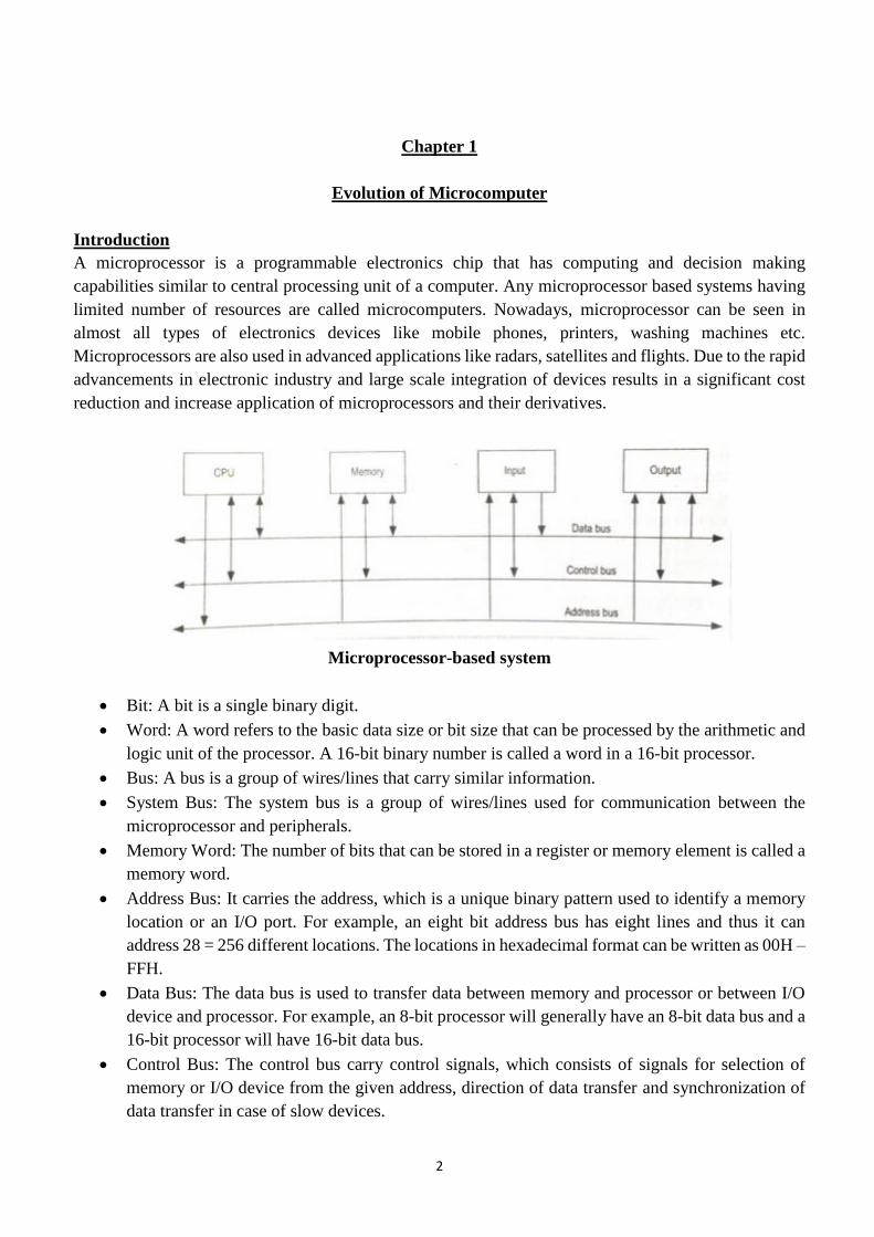
A microprocessor is a programmable electronics chip that has computing and decision making
capabilities similar to central processing unit of a computer. Any microprocessor based systems having
limited number of resources are called microcomputers. Nowadays, microprocessor can be seen in
almost all types of electronics devices like mobile phones, printers, washing machines etc.
Microprocessors are also used in advanced applications like radars, satellites and flights. Due to the rapid
advancements in electronic industry and large scale integration of devices results in a significant cost
reduction and increase application of microprocessors and their derivatives.
Microprocessor-based system
Bit: A bit is a single binary digit.
Word: A word refers to the basic data size or bit size that can be processed by the arithmetic and
logic unit of the processor. A 16-bit binary number is called a word in a 16-bit processor.
Bus: A bus is a group of wires/lines that carry similar information.
System Bus: The system bus is a group of wires/lines used for communication between the
microprocessor and peripherals.
Memory Word: The number of bits that can be stored in a register or memory element is called a
memory word.
Address Bus: It carries the address, which is a unique binary pattern used to identify a memory
location or an I/O port. For example, an eight bit address bus has eight lines and thus it can
address 28 = 256 different locations. The locations in hexadecimal format can be written as 00H –
FFH.
Data Bus: The data bus is used to transfer data between memory and processor or between I/O
device and processor. For example, an 8-bit processor will generally have an 8-bit data bus and a
16-bit processor will have 16-bit data bus.
Control Bus: The control bus carry control signals, which consists of signals for selection of
memory or I/O device from the given address, direction of data transfer and synchronization of
data transfer in case of slow devices.

3
A typical microprocessor consists of arithmetic and logic unit (ALU) in association with control unit to
process the instruction execution. Almost all the microprocessors are based on the principle of
store-program concept. In store-program concept, programs or instructions are sequentially stored in the
memory locations that are to be executed. To do any task using a microprocessor, it is to be programmed
by the user. So the programmer must have idea about its internal resources, features and supported
instructions. Each microprocessor has a set of instructions, a list which is provided by the microprocessor
manufacturer. The instruction set of a microprocessor is provided in two forms: binary machine code and
mnemonics.
Microprocessor communicates and operates in binary numbers 0 and 1. The set of instructions in the
form of binary patterns is called a machine language and it is difficult for us to understand. Therefore, the
binary patterns are given abbreviated names, called mnemonics, which forms the assembly language.
The conversion of assembly-level language into binary machine-level language is done by using an
application called assembler.
Technology Used:
The semiconductor manufacturing technologies used for chips are:
Transistor-Transistor Logic (TTL)
Emitter Coupled Logic (ECL)
Complementary Metal-Oxide Semiconductor (CMOS)
Classification of Microprocessors:
Based on their specification, application and architecture microprocessors are classified.
Based on size of data bus:
4-bit microprocessor
8-bit microprocessor
16-bit microprocessor
32-bit microprocessor
Based on application:
General-purpose microprocessor- used in general computer system and can be used by
programmer for any application. Examples, 8085 to Intel Pentium.
Microcontroller- microprocessor with built-in memory and ports and can be programmed for any
generic control application. Example, 8051.
Special-purpose processors- designed to handle special functions required for an application.
Examples, digital signal processors and application-specific integrated circuit (ASIC) chips.
Based on architecture:
Reduced Instruction Set Computer (RISC) processors
Complex Instruction Set Computer (CISC) processors
The concept and architecture of a microcomputer
A microcomputer is a computer built on the basis of a microprocessor i.e. a processor implemented as
an integrated circuit. Since all processors are now produced in the form of integrated circuits, we can

4
say that all computers are microcomputers. The general method for constructing microcomputers
consists in connecting to the microprocessor busses additional sub-systems such as memories and
peripheral device controllers (input/output units).
The basic block diagram of a simple microcomputer is shown in the figure below. We can see there a
microprocessor with three its busses going out: data bus, address bus and control bus. To these busses,
the following devices are connected: operational memory composed of RAM (Random Access
Memory)and ROM (Read Only Memory) memories, as well as input/output units to which peripheral
devices are connected.
Simple microcomputer
A more developed block diagram of a microcomputer is shown in the figure below. Besides RAM and
ROM memories, more input/output units are connected to the microprocessor.
These input/output units include:
parallel input/output controller in short - parallel I/O, parallel interface
serial input/output controller in short - serial I/O, serial interface
interrupt controller (handler)
timer/counter controller
Direct Memory Access (DMA) controller
5
General scheme of simple microcomputer
Parallel input/output controller maintains information exchange with peripheral devices, which send
data in the parallel form. Examples of such devices are printers, display monitor, hard and floppy disk
memories, keyboard. The activity of the controller is supervised by the microprocessor, which
intervenes on each transfer of data by execution of respective instructions of data read or write from (to)
the controller. The controller itself transfers data from its internal memory (registers) to peripheral
devices.
The serial input/output controller maintains information exchange with peripheral devices, which
send data in the serial form. Examples of such devices are a mouse and a modem for interconnections
through telephone network. The controller implements in hardware conversion of serial data into their
parallel form and vice versa (with the use of serial/parallel registers). The functioning of the controller
is controlled by the microprocessor, which intervenes on each termination of data conversion by
execution of respective data read or writes instructions.
Interrupt controller provides servicing interrupts coming in parallel from many external devices. Its
task consists in receiving interrupt requests, registering them, performing selection to choose one
which is to be serviced by the processor. The controller communicates with the processor to enable
sending the identifier of the selected interrupt and to exchange control signals. The interrupt controller
is supervised by the processor, which services the interrupt after receiving the interrupt from the
controller.
The DMA controller enables parallel data exchange between external devices and the operational
memory without involvement of the processor. This controller enables autonomous data transfers
to/from operational memory. These transfers do not engage the processor, which can proceed with
computations at the same time.

6
The Microprocessor's Impact on Society
Today, we literally swim in a sea of silicon. There are dozens of chips in every car and dozens in every
office. Microprocessors in the form of watches, pagers, cellular phones, and Sharp Wizard's adorn our
bodies as jewelry. Beyond embedded systems, the rapid rise of the Internet now appears to be on the
verge of ensuring that the personal computer truly becomes ubiquitous. Where in the past PCs have been
concentrated in the workplace and scattered in the homes of the wealthier third of American society, the
Internet is almost certain to lower the final obstacles and make it possible to create a new class of
information appliances that will extend the reach of the Net until it matches that of television or the
telephone. Microprocessors are everywhere, but how is modern life different? In many areas the advent
of microelectronics obviously does have clear benefits. That can be seen in the effect of computing
technology on the disabled; the transformation of certain kinds of boring and dangerous manual labor;
advances in medical technology and weather forecasting. Indeed the easy answer is that microprocessors
have transformed modern society. They affect the way we work and play, the way we travel and
communicate. They offer remarkable processing power at infinitesimal cost.
7
Chapter 2
Architecture of Microprocessor
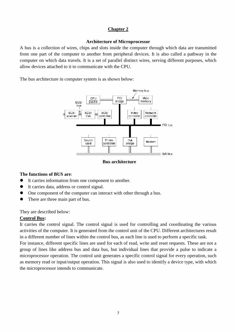
A bus is a collection of wires, chips and slots inside the computer through which data are transmitted
from one part of the computer to another from peripheral devices. It is also called a pathway in the
computer on which data travels. It is a set of parallel distinct wires, serving different purposes, which
allow devices attached to it to communicate with the CPU.
The bus architecture in computer system is as shown below:
Bus architecture
The functions of BUS are:
It carries information from one component to another.
It carries data, address or control signal.
One component of the computer can interact with other through a bus.
There are three main part of bus.
They are described below:
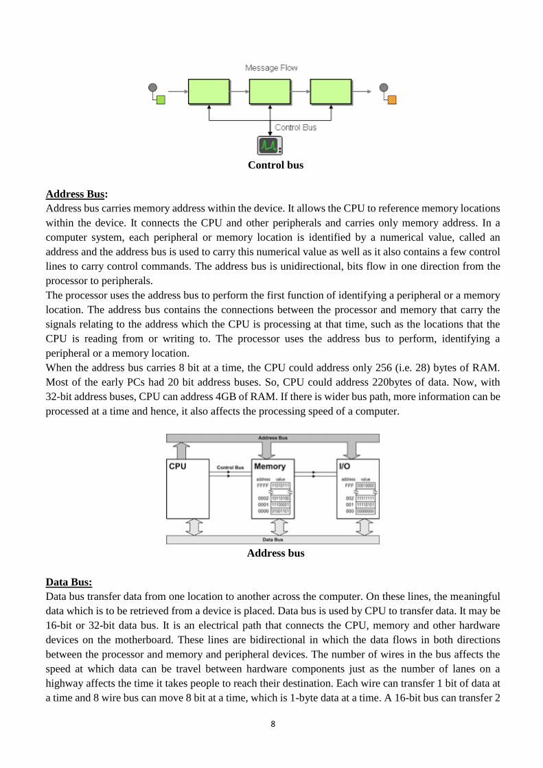
Control Bus:
It carries the control signal. The control signal is used for controlling and coordinating the various
activities of the computer. It is generated from the control unit of the CPU. Different architectures result
in a different number of lines within the control bus, as each line is used to perform a specific task.
For instance, different specific lines are used for each of read, write and reset requests. These are not a
group of lines like address bus and data bus, but individual lines that provide a pulse to indicate a
microprocessor operation. The control unit generates a specific control signal for every operation, such
as memory read or input/output operation. This signal is also used to identify a device type, with which
the microprocessor intends to communicate.
8
Control bus
Address Bus:
Address bus carries memory address within the device. It allows the CPU to reference memory locations
within the device. It connects the CPU and other peripherals and carries only memory address. In a
computer system, each peripheral or memory location is identified by a numerical value, called an
address and the address bus is used to carry this numerical value as well as it also contains a few control
lines to carry control commands. The address bus is unidirectional, bits flow in one direction from the
processor to peripherals.
The processor uses the address bus to perform the first function of identifying a peripheral or a memory
location. The address bus contains the connections between the processor and memory that carry the
signals relating to the address which the CPU is processing at that time, such as the locations that the
CPU is reading from or writing to. The processor uses the address bus to perform, identifying a
peripheral or a memory location.
When the address bus carries 8 bit at a time, the CPU could address only 256 (i.e. 28) bytes of RAM.
Most of the early PCs had 20 bit address buses. So, CPU could address 220bytes of data. Now, with
32-bit address buses, CPU can address 4GB of RAM. If there is wider bus path, more information can be
processed at a time and hence, it also affects the processing speed of a computer.
Address bus
Data Bus:
Data bus transfer data from one location to another across the computer. On these lines, the meaningful
data which is to be retrieved from a device is placed. Data bus is used by CPU to transfer data. It may be
16-bit or 32-bit data bus. It is an electrical path that connects the CPU, memory and other hardware
devices on the motherboard. These lines are bidirectional in which the data flows in both directions
between the processor and memory and peripheral devices. The number of wires in the bus affects the
speed at which data can be travel between hardware components just as the number of lanes on a
highway affects the time it takes people to reach their destination. Each wire can transfer 1 bit of data at
a time and 8 wire bus can move 8 bit at a time, which is 1-byte data at a time. A 16-bit bus can transfer 2

9
bytes. 32 bits can transfer 4 bytes and so on. Intel 80286 microprocessor used16 bit data bus and Intel
80386 used 32-bit data bus. When the data bus width grows larger, more data can be transferred.
The transmission of the data on bus lines takes place between approximately 1M baud for the
microcomputer to about 1000 M baud or more for the large more expensive computers (1 baud = 1
bit/sec). Communication between the different units of a processing system is carried out along address
and data bus and also along various control lines. All control operations are governed by the master
timing source and clock.
data bus
Bus organization of 8085
The microprocessor MPU performs various operations with peripheral devices or a memory location
by using three sets of communication lines called buses: the address bus, the data bus and the control
bus. And these three combined lines is called as system bus.
Bus structure
Address bus:
The address bus is a group of 16 lines generally called as A0 – A15 to carry a 16-bit address of
memory location. In a computer system, each peripheral or memory location is identified by a binary
number called an address. This is similar to the postal address of a house. The address bus is
unidirectional, that means bit flow in only one direction from MPU to peripheral.
MPU carries 16-bit address i.e. 216 = 65,536 or 64K memory locations.
Data Bus:

10
The data bus is a group of eight bidirectional lines used for data flow in both the directions between
MPH and peripheral devices.
The 8 data lines are manipulating 8-bit data ranging from 00 to FF i.e. (28 = 256) numbers from 0000
0000 -1111 1111
This 8 bit data is called as word length and the register size of a microprocessor and MPH is called
8–bit microprocessor.
Control bus:
Control bus is having various single lines used for sending control signals in the form of pulse to the
memory and I/O devices.
The MPU generates specific control signals to perform a particular operations. Some of these control
signals are memory read, memory write, I/O read and I/O write.
Pin diagram of 8085
The 8085 and Its Buses
The 8085 is an 8-bit general purpose microprocessor that can address 64K Byte of memory.
It has 40 pins and uses +5V for power. It can run at a maximum frequency of 3 MHz.
The pins on the chip can be grouped into 6 groups:
Address Bus.
Data Bus.
Control and Status Signals.
Power supply and frequency.
Externally Initiated Signals.
Serial I/O ports.
8085 Pin description
Higher Order Address pins- A15 – A8
o The address bus has 8 signal lines A8 – A15 which are unidirectional.
Lower Order Address/ Data Pins- AD7-AD0
11
o These are time multiplexed pins and are DE-multiplexed using the pin ALE
o So, the bits AD0 – AD7 are bi-directional and serve as A0 – A7 and D0 – D7 at the
same time.
o During the execution of the instruction, these lines carry the address bits during the
early part, then during the late parts of the execution, they carry the 8 data bits.
o In order to separate the address from the data, we can use a latch to save the value
before the function of the bits changes.
Control Pins – RD, WR
o These are active low Read & Write pins
Status Pins – ALE, IO/M (active low), S1, S0
o ALE (Address Latch Enable)-Used to DE-multiplex AD7-AD0
o IO/M – Used to select I/O or Memory operation
o S1,S0 – Denote the status of data on data bus
Interrupt Pins – TRAP, RST7.5, RST 6.5, RST 5.5, INTR, INTA
o These are hardware interrupts used to initiate an interrupt service routine stored at
predefined locations of the system memory.
Serial I/O pins – SID (Serial Input Data), SOD (Serial Output Data)
o These pins are used to interface 8085 with a serial device.
Clock Pins- X1, X2, CLK(OUT)
o X1, X2– These are clock input pins. A crystal is connected between these pins such that
fcrystal= 2f8085 where fcrystal= crystal frequency & f8085 = operating frequency of 8085
o CLK(OUT) – This is an auxiliary clock output source
Reset Pins – Reset In (active low), Reset Out
o Reset In is used to reset 8085 whereas Reset Out can be used to reset other devices in
the system
DMA (Direct Memory Access) pins – HOLD, HLDA
o These pins are used when data transfer is to be performed directly between an external
device and the main memory of the system.
Power Supply Pins – +VCC, VSS

12
Architecture of 8085
Function block diagram of 8085
This is the functional Block Diagram of 8085 Microprocessor.
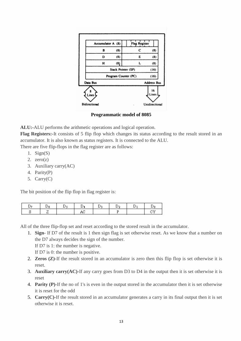
Accumulator:-It is a 8-bit register which is used to perform arithmetical and logical operation. It stores
the output of any operation. It also works as registers for i/o accesses.
Temporary Register:-It is a 8-bit register which is used to hold the data on which the accumulator is
computing operation. It is also called as operand register because it provides operands to ALU.
Registers:-These are general purposes registers. Microprocessor consists 6 general purpose registers of
8-bit each named as B, C, D, E, H and L. Generally theses registers are not used for storing the data
permanently. It carries the 8-bits data. These are used only during the execution of the instructions.
These registers can also be used to carry the 16 bits data by making the pair of 2 registers. The valid
register pairs available are BC, DE HL. We cannot use other pairs except BC, DE and HL. These
registers are programmed by user.
13
Programmatic model of 8085
ALU:-ALU performs the arithmetic operations and logical operation.
Flag Registers:-It consists of 5 flip flop which changes its status according to the result stored in an
accumulator. It is also known as status registers. It is connected to the ALU.
There are five flip-flops in the flag register are as follows:
1. Sign(S)
2. zero(z)
3. Auxiliary carry(AC)
4. Parity(P)
5. Carry(C)
The bit position of the flip flop in flag register is:
All of the three flip-flop set and reset according to the stored result in the accumulator.
1. Sign- If D7 of the result is 1 then sign flag is set otherwise reset. As we know that a number on
the D7 always decides the sign of the number.
If D7 is 1: the number is negative.
If D7 is 0: the number is positive.
2. Zeros (Z)-If the result stored in an accumulator is zero then this flip flop is set otherwise it is
reset.
3. Auxiliary carry(AC)-If any carry goes from D3 to D4 in the output then it is set otherwise it is
reset
4. Parity (P)-If the no of 1's is even in the output stored in the accumulator then it is set otherwise
it is reset for the odd
5. Carry(C)-If the result stored in an accumulator generates a carry in its final output then it is set
otherwise it is reset.

14
Instruction registers (IR):- It is a 8-bit register. When an instruction is fetched from memory
then it is stored in this register.
Instruction Decoder: - Instruction decoder identifies the instructions. It takes the information
from instruction register and decodes the instruction to be performed.
Program Counter:- It is a 16 bit register used as memory pointer. It stores the memory address
of the next instruction to be executed. So we can say that this register is used to sequencing the
program. Generally the memory have 16 bit addresses so that it has 16 bit memory.
The program counter is set to 0000H.
Stack Pointer: - It is also a 16 bit register used as memory pointer. It points to the memory
location called stack. Generally stack is a reserved portion of memory where information can be
stores or taken back together.
Timing and Control Unit: - It provides timing and control signal to the microprocessor to
perform the various operations. It has three control signals. It controls all external and internal
circuits. It operates with reference to clock signals. It synchronizes all the data transfers.
There are three control signal:
1. ALE-Arithmetic Latch Enable, It provides control signal to synchronize the components of
microprocessor.
2. RD- This is active low used for reading operation.
3. WR-This is active low used for writing operation.
There are three status signal used in microprocessor S0, S1 and IO/M. It changes its status
according the provided input to these pins.
Serial Input Output Control-There are two pins in this unit. This unit is used for serial data
communication.
Interrupt Unit-There are 6 interrupt pins in this unit. Generally an external hardware is
connected to these pins. These pins provide interrupt signal sent by external hardware to
microprocessor and microprocessor sends acknowledgement for receiving the interrupt signal.
Generally INTA is used for acknowledgement.

15
Register Section:-Many registers has been used in microprocessor.
It consists of PIPO (Parallel Input Parallel Output) register.
What is an Opcode?
Opcode is nothing but the machine language instruction which denotes the microprocessor about what
operation should be performed on the specific data. Microprocessor converts the instruction into suitable
machine language, so that it can understand the operation to be performed and executes it.
Consider MVI A, 18H.
When the above instruction is to be executed, the microprocessor gets the Opcode for MVI A and
performs the necessary operation on the data which is 18H in this case. The Opcode for MVI A is 3EH.
So the microprocessor first reads this Opcode from the instruction and then performs the operation
specified by Opcode over the data given.
Now let us assume we want to store the above instruction in a specific address say 5500H. We know that
in 8085 processor only one byte can be stored in each address location. Therefore the Opcode 3EH is
stored at the location 5500H and the data 18H is stored at the next location 5501H.
Schematic diagram of control signal generation
READ Operation:
During T1 state, microprocessor uses IO/M(bar), S0, S1 signals are used to instruct
microprocessor to fetch opcode.
Thus when IO/M(bar)=0, S0=S1= 1, it indicates opcode fetch operation.
During this operation 8085 transmits 16-bit address and also uses ALE signal for address
latching.
At T2 state microprocessor uses read signal and make data ready from that memory location to
read opcode from memory and at the same time program counter increments by 1 and points next
instruction to be fetched.
In this state microprocessor also checks READY input signal, if this pin is at low logic level ie. '0'
then microprocessor adds wait state immediately between T2 and T3.
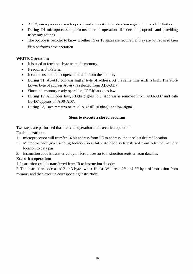
16
At T3, microprocessor reads opcode and stores it into instruction register to decode it further.
During T4 microprocessor performs internal operation like decoding opcode and providing
necessary actions.
The opcode is decoded to know whether T5 or T6 states are required, if they are not required then
碌 p performs next operation.
WRITE Operation:
It is used to fetch one byte from the memory.
It requires 3 T-States.
It can be used to fetch operand or data from the memory.
During T1, A8-A15 contains higher byte of address. At the same time ALE is high. Therefore
Lower byte of address A0-A7 is selected from AD0-AD7.
Since it is memory ready operation, IO/M(bar) goes low.
During T2 ALE goes low, RD(bar) goes low. Address is removed from AD0-AD7 and data
D0-D7 appears on AD0-AD7.
During T3, Data remains on AD0-AD7 till RD(bar) is at low signal.
Steps to execute a stored program
Two steps are performed that are fetch operation and execution operation.
Fetch operation: -
1. microprocessor will transfer 16 bit address from PC to address line to select desired location
2. Microprocessor gives reading location so 8 bit instruction is transferred from selected memory
location to data pin
3. instruction code is transferred by mi9croprocessor to instruction register from data bus
Execution operation:-
1. Instruction code is transferred from IR to instruction decoder
2. The instruction code as of 2 or 3 bytes when 1st ckt. Will read 2nd and 3rd byte of instruction from
memory and then execute corresponding instruction.

17
Chapter 3
Instruction Timing and Cycle
An instruction cycle (also known as the fetch–decode–execute cycle or the fetch-execute cycle) is the
basic operational process of a computer. It is the process by which a computer retrieves
a program instruction from its memory, determines what actions the instruction dictates, and carries out
those actions. This cycle is repeated continuously by a computer's central processing unit (CPU),
from boot-up to when the computer is shut down.
In simpler CPU's the instruction cycle is executed sequentially, each instruction being processed before
the next one is started. In most modern CPU's the instruction cycles are instead executed concurrently,
and often in parallel, through an instruction pipeline: the next instruction starts being processed before
the previous instruction has finished, which is possible because the cycle is broken up into separate steps.
1. Initiating the cycle
The cycle starts immediately when power is applied to the system using an initial PC value that
is predefined for the system architecture
Typically this address points to instructions in a read-only memory (ROM) (not the random
access memory or RAM) which begins the process of loading the operating system.
2. Fetch the Instruction
Step 1 of the Instruction Cycle is called the Fetch Cycle. This step is the same for each instruction.
i. The CPU sends PC to the MAR and sends a READ command on the control bus
ii. In response to the read command (with address equal to PC), the memory returns the data
stored at the memory location indicated by PC on the data bus.
iii. The CPU copies the data from the data bus into its MDR (also known as MBR)
iv. A fraction of a second later, the CPU copies the data from the MDR to the Instruction Register
(IR)
v. The PC is incremented so that it points to the following instruction in memory. This step
prepares the CPU for the next cycle. The Control Unit fetches the instruction's address from
the Memory Unit
3. Decode the Instruction
Step 2 of the instruction Cycle is called the Decode Cycle. The decoding process allows the
CPU to determine what instruction is to be performed, so that the CPU can tell how many
operands it needs to fetch in order to perform the instruction.
The opcode fetched from the memory is decoded for the next steps and moved to the
appropriate registers. The decoding is done by the CPU's Control Unit.
4. Read the effective address
Step 3 is deciding which operation it is. If this is a Memory operation - in this step the computer
checks if it's a direct or indirect memory operation:
Direct memory instruction - Nothing is being done.
Indirect memory instruction - The effective address is being read from the memory. If this is a
I/O or Register instruction - the computer checks its kind and executes the instruction.

18
5. Execute the Instruction
Step 4 of the Instruction Cycle is the Execute Cycle. Here, the function of the instruction is
performed.
If the instruction involves arithmetic or logic, the Arithmetic Logic Unit is utilized. This is the
only stage of the instruction cycle that is useful from the perspective of the end user.
Everything else is overhead required to make the execute stage happen.
Machine cycle
A machine cycle, also called a processor cycle or a instruction cycle, is the basic operation performed
by a central processing unit (CPU). A CPU is the main logic unit of a computer.
A machine cycle consists of a sequence of three steps that is performed continuously and at a rate of
millions per second while a computer is in operation. They are fetch, decode and execute. There also is
a fourth step, store, in which input and output from the other three phases is stored in memory for later
use; however, no actual processing is performed during this step.
In the fetch step, the control unit requests that main memory provide it with the instruction that is
stored at the address (i.e., location in memory) indicated by the control unit's program counter.
The control unit is a part of the CPU that also decodes the instruction in the instruction register.
A register is a very small amount of very fast memory that is built into the CPU in order to speed up its
operations by providing quick access to commonly used values; instruction registers are registers that
hold the instruction being executed by the CPU. Decoding the instructions in the instruction register
involves breaking the operand field into its components based on the instructions opcode.
Opcode (an abbreviation of operation code) is the portion of a machine language instruction that
specifies what operation is to be performed by the CPU. Machine language, also called machine code,
refers to instructions coded in patterns of bits (i.e., zeros and ones) that are directly readable and
executable by a CPU.
A program counter, also called the instruction pointer in some computers, is a register that indicates
where the computer is in its instruction sequence. It holds either the address of the instruction currently
being executed or the address of the next instruction to be executed, depending on the details of the
particular computer. The program counter is automatically incremented for each machine cycle so that
instructions are normally retrieved sequentially from memory.
The control unit places these instructions into its instruction register and then increments the program
counter so that it contains the address of the next instruction stored in memory. It then executes the
instruction by activating the appropriate circuitry to perform the requested task. As soon as the
instruction has been executed, it restarts the machine cycle, beginning with the fetch step.
T states
One complete cycle of clock is called as T-state as shown in the above figure. A T-state is measured from
the falling edge of one clock pulse to the falling edge of the next clock pulse. Various versions of 8086
have maximum clock frequency from 5MHz to 10MHz. Hence the minimum time for one T-state is
between 100 to 200 nsec.

19
Instruction Execution And Timing Diagram:
Each instruction in 8085 microprocessor consists of two part- operation code (opcode) and operand. The
opcode is a command such as ADD and the operand is an object to be operated on, such as a byte or the
content of a register.
Instruction Cycle: The time taken by the processor to complete the execution of an instruction. An
instruction cycle consists of one to six machine cycles.
Machine Cycle: The time required to complete one operation; accessing either the memory or I/O
device. A machine cycle consists of three to six T-states.
T-State: Time corresponding to one clock period. It is the basic unit to calculate execution of
instructions or programs in a processor.
To execute a program, 8085 performs various operations as:
Opcode fetch
Operand fetch
Memory read/write
I/O read/write
External communication functions are:
Memory read/write
I/O read/write
Interrupt request acknowledge
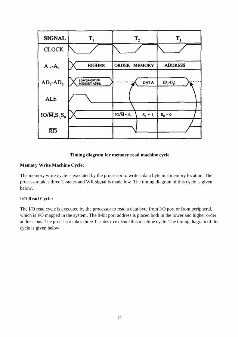
Opcode Fetch Machine Cycle:
It is the first step in the execution of any instruction. The timing diagram of this cycle is given below
The following points explain the various operations that take place and the signals that are changed
during the execution of opcode fetch machine cycle:
T1 clock cycle
i. The content of PC is placed in the address bus; AD0 - AD7 lines contains lower bit address and A8 –
A15 contains higher bit address.
ii. M IO/ signal is low indicating that a memory location is being accessed. S1 and S0 also changed to
the levels as indicated in Table 1.
iii. ALE is high, indicates that multiplexed AD0 – AD7 act as lower order bus.
T2 clock cycle
i. Multiplexed address bus is now changed to data bus.
ii. The RD signal is made low by the processor. This signal makes the memory device load the data bus
with the contents of the location addressed by the processor.

20
T3 clock cycle
i. The opcode available on the data bus is read by the processor and moved to the instruction
register. ii. The RD signal is deactivated by making it logic 1.
T4 clock cycle
i. The processor decode the instruction in the instruction register and generate the necessary
control signals to execute the instruction. Based on the instruction further operations such as
fetching, writing into memory etc takes place.
Timing diagram for opcode fetch cycle
Memory Read Machine Cycle:
The memory read cycle is executed by the processor to read a data byte from memory. The machine
cycle is exactly same to opcode fetch except: a) It has three T-states b) The S0 signal is set to 0. The
timing diagram of this cycle is given in Fig.
21
Timing diagram for memory read machine cycle
Memory Write Machine Cycle:
The memory write cycle is executed by the processor to write a data byte in a memory location. The
processor takes three T-states and WR signal is made low. The timing diagram of this cycle is given
below.
I/O Read Cycle:
The I/O read cycle is executed by the processor to read a data byte from I/O port or from peripheral,
which is I/O mapped in the system. The 8-bit port address is placed both in the lower and higher order
address bus. The processor takes three T-states to execute this machine cycle. The timing diagram of this
cycle is given below

22
Timing diagram for memory write machine cycle
Timing diagram I/O read machine cycle

23
I/O Write Cycle:
The I/O write cycle is executed by the processor to write a data byte to I/O port or to a peripheral, which
is I/O mapped in the system. The processor takes three T-states to execute this machine cycle. The timing
diagram of this cycle is given in dia.
Timing diagram I/O write machine cycle
Ex: Timing diagram for IN 80H.
24
Chapter – 4
Programming (with respect to8085 microprocessor)
Assembly languages
An assembly (or assembler) language, often abbreviated asm, is a low-level programming language for
a computer, or other programmable device, in which there is a very strong (but often not one-to-one)
correspondence between the language and the architecture's machine code instructions. Each assembly
language is specific to a particular computer architecture. In contrast, most high-level programming
languages are generally portable across multiple architectures but require interpreting or compiling.
Assembly language may also be called symbolic machine code.
Machine language
Machine code or machine language is a set of instructions executed directly by a computer's central
processing unit (CPU). Each instruction performs a very specific task, such as a load, a jump, or
an ALU operation on a unit of data in a CPU register or memory. Every program directly executed by a
CPU is made up of a series of such instructions. (The phrase 'directly executed' needs some clarification;
machine code is by definition the lowest level of programming detail visible to the programmer, but
internally many processors use microcode or optimize and transform machine code instructions into
sequences of micro-ops in a sophisticated way.)
Mnemonics
Mnemonics allow users to access quickly a wide variety of commands, services, programs and functions
without the need to type out extended phrases. One example of a mnemonic code is the term "inc," which
on an Intel microprocessor refers to the command "increase by one." Rather than type the entire phrase,
the letters "inc" can be entered. Mnemonic code derives from the concept of traditional mnemonics in
which abbreviations, rhymes or simple stories are used to help people remember information.
Instruction Set and Execution In 8085
Based on the design of the ALU and decoding unit, the microprocessor manufacturer provides
instruction set for every microprocessor. The instruction set consists of both machine code and
mnemonics.
An instruction is a binary pattern designed inside a microprocessor to perform a specific function. The
entire group of instructions that a microprocessor supports is called instruction set. Microprocessor
instructions can be classified based on the parameters such functionality, length and operand addressing.
Classification based on functionality:
I. Data transfer operations: This group of instructions copies data from source to destination. The
content of the source is not altered.
II. Arithmetic operations: Instructions of this group perform operations like addition, subtraction,
increment & decrement. One of the data used in arithmetic operation is stored in accumulator and
the result is also stored in accumulator.
III. Logical operations: Logical operations include AND, OR, EXOR, NOT. The operations like AND,
OR and EXOR uses two operands, one is stored in accumulator and other can be any register or
25
memory location. The result is stored in accumulator. NOT operation requires single operand,
which is stored in accumulator.
IV. Branching operations: Instructions in this group can be used to transfer program sequence from
one memory location to another either conditionally or unconditionally. V. Machine control
operations: Instruction in this group control execution of other instructions and control operations
like interrupt, halt etc.
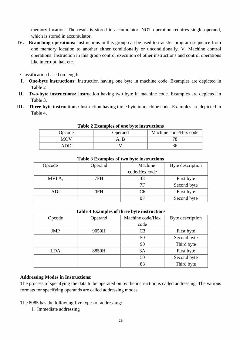
Classification based on length:
I. One-byte instructions: Instruction having one byte in machine code. Examples are depicted in
Table 2
II. Two-byte instructions: Instruction having two byte in machine code. Examples are depicted in
Table 3.
III. Three-byte instructions: Instruction having three byte in machine code. Examples are depicted in
Table 4.
Table 2 Examples of one byte instructions
Opcode Operand Machine code/Hex code
MOV A, B 78
ADD M 86
Table 3 Examples of two byte instructions
Opcode Operand Machine
code/Hex code
Byte description
MVI A, 7FH 3E First byte
7F Second byte
ADI 0FH C6 First byte
0F Second byte
Table 4 Examples of three byte instructions
Opcode Operand Machine code/Hex
code
Byte description
JMP 9050H C3 First byte
50 Second byte
90 Third byte
LDA 8850H 3A First byte
50 Second byte
88 Third byte
Addressing Modes in Instructions:
The process of specifying the data to be operated on by the instruction is called addressing. The various
formats for specifying operands are called addressing modes.
The 8085 has the following five types of addressing:
I. Immediate addressing

26
II. Memory direct addressing
III. Register direct addressing
IV. Indirect addressing
V. Implicit addressing
Immediate Addressing:
In this mode, the operand given in the instruction - a byte or word – transfers to the destination register or
memory location.
Ex: MVI A, 9AH
The operand is a part of the instruction.
The operand is stored in the register mentioned in the instruction.
Memory Direct Addressing:
Memory direct addressing moves a byte or word between a memory location and register. The memory
location address is given in the instruction.
Ex: LDA 850FH
This instruction is used to load the content of memory address 850FH in the accumulator.
Register Direct Addressing:
Register direct addressing transfer a copy of a byte or word from source register to destination register.
Ex: MOV B, C
It copies the content of register C to register B.
Indirect Addressing:
Indirect addressing transfers a byte or word between a register and a memory location.
Ex: MOV A, M
Here the data is in the memory location pointed to by the contents of HL pair. The data is moved to the
accumulator.
Implicit Addressing
In this addressing mode the data itself specifies the data to be operated upon.
Ex: CMA
The instruction complements the content of the accumulator. No specific data or operand is mentioned in
the instruction.
27
INSTRUCTION SET OF 8085
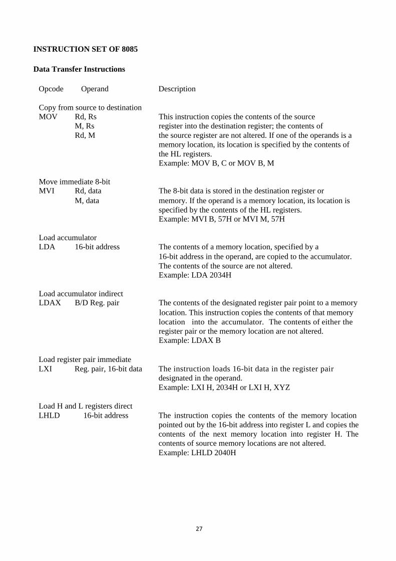
Data Transfer Instructions
Opcode Operand Description
Copy from source to destination
MOV Rd, Rs This instruction copies the contents of the source M, Rs register into the destination register; the contents of Rd, M the source register are not altered. If one of the operands is a memory location, its location is specified by the contents of the HL registers. Example: MOV B, C or MOV B, M
Move immediate 8-bit MVI Rd, data The 8-bit data is stored in the destination register or
M, data memory. If the operand is a memory location, its location is specified by the contents of the HL registers. Example: MVI B, 57H or MVI M, 57H
Load accumulator
LDA 16-bit address The contents of a memory location, specified by a 16-bit address in the operand, are copied to the accumulator. The contents of the source are not altered. Example: LDA 2034H
Load accumulator indirect LDAX B/D Reg. pair The contents of the designated register pair point to a memory
location. This instruction copies the contents of that memory location into the accumulator. The contents of either the register pair or the memory location are not altered. Example: LDAX B
Load register pair immediate
LXI Reg. pair, 16-bit data The instruction loads 16-bit data in the register pair
designated in the operand.
Example: LXI H, 2034H or LXI H, XYZ
Load H and L registers direct
LHLD 16-bit address The instruction copies the contents of the memory location
pointed out by the 16-bit address into register L and copies the
contents of the next memory location into register H. The
contents of source memory locations are not altered.
Example: LHLD 2040H
28
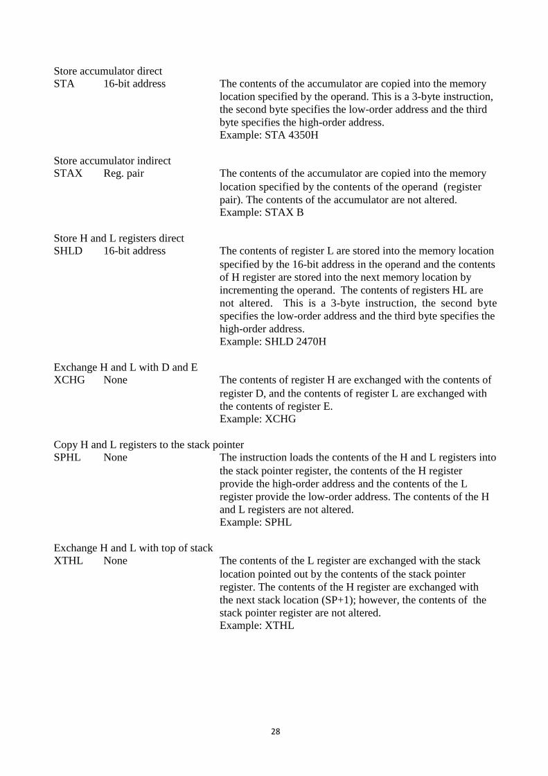
Store accumulator direct STA 16-bit address The contents of the accumulator are copied into the memory
location specified by the operand. This is a 3-byte instruction, the second byte specifies the low-order address and the third byte specifies the high-order address. Example: STA 4350H
Store accumulator indirect STAX Reg. pair The contents of the accumulator are copied into the memory
location specified by the contents of the operand (register pair). The contents of the accumulator are not altered. Example: STAX B
Store H and L registers direct SHLD 16-bit address The contents of register L are stored into the memory location
specified by the 16-bit address in the operand and the contents of H register are stored into the next memory location by incrementing the operand. The contents of registers HL are not altered. This is a 3-byte instruction, the second byte specifies the low-order address and the third byte specifies the high-order address. Example: SHLD 2470H
Exchange H and L with D and E XCHG None The contents of register H are exchanged with the contents of
register D, and the contents of register L are exchanged with the contents of register E. Example: XCHG
Copy H and L registers to the stack pointer
SPHL None The instruction loads the contents of the H and L registers into the stack pointer register, the contents of the H register provide the high-order address and the contents of the L register provide the low-order address. The contents of the H and L registers are not altered. Example: SPHL
Exchange H and L with top of stack
XTHL None The contents of the L register are exchanged with the stack location pointed out by the contents of the stack pointer register. The contents of the H register are exchanged with the next stack location (SP+1); however, the contents of the stack pointer register are not altered. Example: XTHL
29
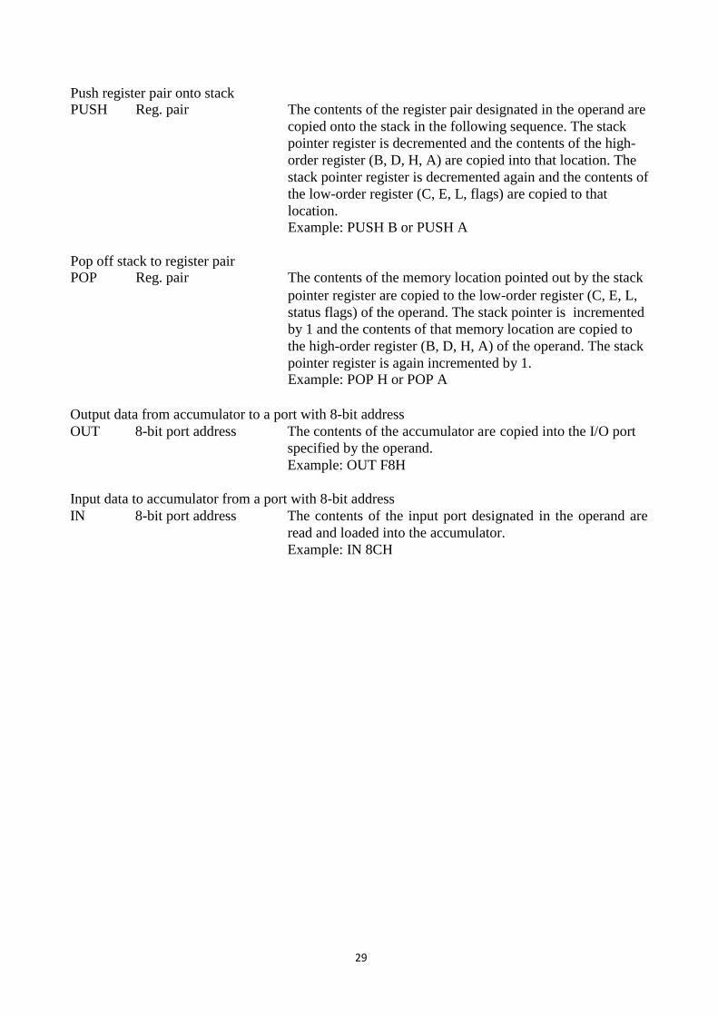
Push register pair onto stack PUSH Reg. pair The contents of the register pair designated in the operand are
copied onto the stack in the following sequence. The stack pointer register is decremented and the contents of the high- order register (B, D, H, A) are copied into that location. The stack pointer register is decremented again and the contents of the low-order register (C, E, L, flags) are copied to that location. Example: PUSH B or PUSH A
Pop off stack to register pair POP Reg. pair The contents of the memory location pointed out by the stack
pointer register are copied to the low-order register (C, E, L, status flags) of the operand. The stack pointer is incremented by 1 and the contents of that memory location are copied to the high-order register (B, D, H, A) of the operand. The stack pointer register is again incremented by 1. Example: POP H or POP A
Output data from accumulator to a port with 8-bit address
OUT 8-bit port address The contents of the accumulator are copied into the I/O port
specified by the operand.
Example: OUT F8H
Input data to accumulator from a port with 8-bit address
IN 8-bit port address The contents of the input port designated in the operand are
read and loaded into the accumulator.
Example: IN 8CH

30
Arithmetic Instructions
Opcode Operand Description
Add register or memory to accumulator
ADD R The contents of the operand (register or memory) are M added to the contents of the accumulator and the result is stored in the accumulator. If the operand is a memory location, its location is specified by the contents of the HL registers. All flags are modified to reflect the result of the addition. Example: ADD B or ADD M
Add register to accumulator with carry ADC R The contents of the operand (register or memory) and
M the Carry flag are added to the contents of the accumulator and the result is stored in the accumulator. If the operand is a memory location, its location is specified by the contents of the HL registers. All flags are modified to reflect the result of the addition. Example: ADC B or ADC M
Add immediate to accumulator
ADI 8-bit data The 8-bit data (operand) is added to the contents of the accumulator and the result is stored in the accumulator. All flags are modified to reflect the result of the addition. Example: ADI 45H
Add immediate to accumulator with carry ACI 8-bit data The 8-bit data (operand) and the Carry flag are added to the
contents of the accumulator and the result is stored in the accumulator. All flags are modified to reflect the result of the addition. Example: ACI 45H
Add register pair to H and L registers DAD Reg. pair The 16-bit contents of the specified register pair are added to
the contents of the HL register and the sum is stored in the HL register. The contents of the source register pair are not altered. If the result is larger than 16 bits, the CY flag is set. No other flags are affected. Example: DAD H

31
Subtract register or memory from accumulator
SUB R The contents of the operand (register or memory ) are M subtracted from the contents of the accumulator, and the result is stored in the accumulator. If the operand is a memory location, its location is specified by the contents of the HL registers. All flags are modified to reflect the result of the subtraction. Example: SUB B or SUB M
Subtract source and borrow from accumulator SBB R The contents of the operand (register or memory ) and
M the Borrow flag are subtracted from the contents of the accumulator and the result is placed in the accumulator. If the operand is a memory location, its location is specified by the contents of the HL registers. All flags are modified to reflect the result of the subtraction. Example: SBB B or SBB M
Subtract immediate from accumulator SUI 8-bit data The 8-bit data (operand) is subtracted from the contents of the
accumulator and the result is stored in the accumulator. All flags are modified to reflect the result of the subtraction. Example: SUI 45H
Subtract immediate from accumulator with borrow
SBI 8-bit data The 8-bit data (operand) and the Borrow flag are subtracted
from the contents of the accumulator and the result is stored in
the accumulator. All flags are modified to reflect the result of the subtracion.
Example: SBI 45H
Increment register or memory by 1 INR R The contents of the designated register or memory) are
M incremented by 1 and the result is stored in the same place. If the operand is a memory location, its location is specified by the contents of the HL registers. Example: INR B or INR M
Increment register pair by 1
INX R The contents of the designated register pair are incremented by
1 and the result is stored in the same place.
Example: INX H

32
Decrement register or memory by 1
DCR R The contents of the designated register or memory are
M decremented by 1 and the result is stored in the same place. If
the operand is a memory location, its location is specified by
the contents of the HL registers.
Example: DCR B or DCR M
Decrement register pair by 1
DCX R The contents of the designated register pair are decremented by
1 and the result is stored in the same place.
Example: DCX H
Decimal adjust accumulator
DAA none The contents of the accumulator are changed from a binary
value to two 4-bit binary coded decimal (BCD) digits. This is
the only instruction that uses the auxiliary flag to perform the
binary to BCD conversion, and the conversion procedure is
described below. S, Z, AC, P, CY flags are altered to reflect the
results of the operation.
If the value of the low-order 4-bits in the accumulator is greater
than 9 or if AC flag is set, the instruction adds 6 to the
low-order four bits.
If the value of the high-order 4-bits in the accumulator is
greater than 9 or if the Carry flag is set, the instruction adds 6 to
the high-order four bits.
Example: DAA

33
Branching Instructions
Opcode Operand Description
Jump unconditionally
JMP 16-bit address The program sequence is transferred to the memory location
specified by the 16-bit address given in the operand.
Example: JMP 2034H or JMP XYZ
Jump conditionally
Operand: 16-bit address
The program sequence is transferred to the memory location
specified by the 16-bit address given in the operand based on
the specified flag of the PSW as described below.
Example: JZ 2034H or JZ XYZ
Opcode Description Flag Status
JC Jump on Carry CY = 1
JNC Jump on no Carry CY = 0
JP Jump on positive S = 0
JM Jump on minus S = 1
JZ Jump on zero Z = 1
JNZ Jump on no zero Z = 0
JPE Jump on parity even P = 1 JPO Jump on parity odd P = 0
34
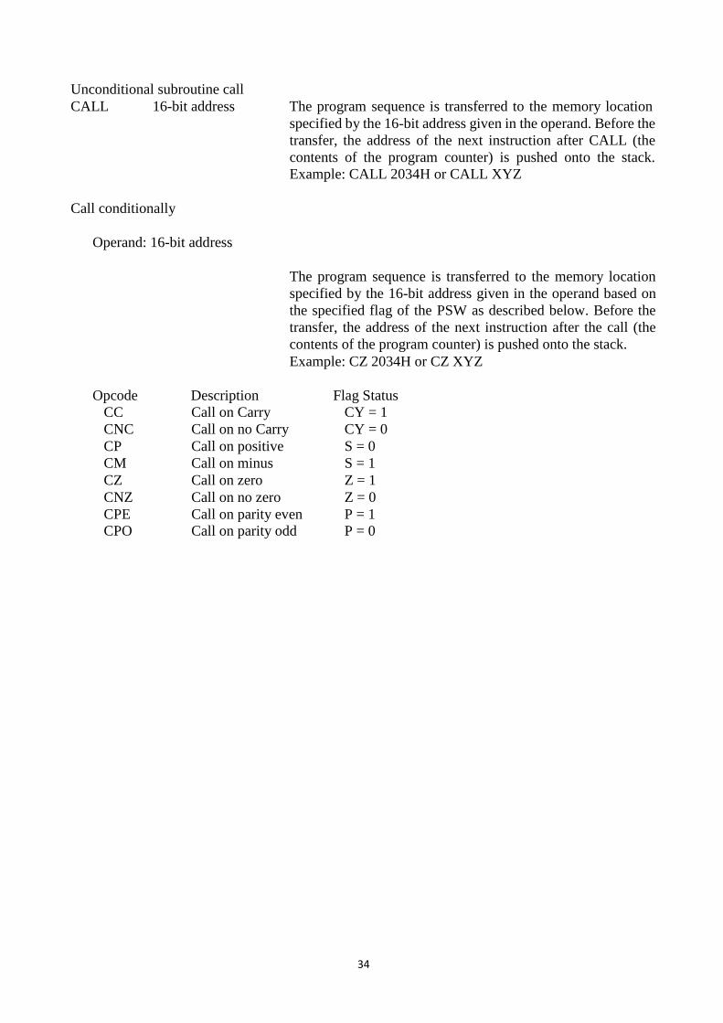
Unconditional subroutine call
CALL 16-bit address The program sequence is transferred to the memory location
specified by the 16-bit address given in the operand. Before the
transfer, the address of the next instruction after CALL (the
contents of the program counter) is pushed onto the stack.
Example: CALL 2034H or CALL XYZ
Call conditionally
Operand: 16-bit address
The program sequence is transferred to the memory location
specified by the 16-bit address given in the operand based on
the specified flag of the PSW as described below. Before the
transfer, the address of the next instruction after the call (the
contents of the program counter) is pushed onto the stack.
Example: CZ 2034H or CZ XYZ
Opcode Description Flag Status
CC Call on Carry CY = 1
CNC Call on no Carry CY = 0
CP Call on positive S = 0
CM Call on minus S = 1
CZ Call on zero Z = 1
CNZ Call on no zero Z = 0
CPE Call on parity even P = 1
CPO Call on parity odd P = 0

35
Return from subroutine unconditionally
RET none The program sequence is transferred from the subroutine to the
calling program. The two bytes from the top of the stack are
copied into the program counter, and program execution begins
at the new address.
Example: RET
Return from subroutine conditionally
Operand: none
The program sequence is transferred from the subroutine to the
calling program based on the specified flag of the PSW as
described below. The two bytes from the top of the stack are
copied into the program counter, and program execution
begins at the new address.
Example: RZ
Opcode Description Flag Status
RC Return on Carry CY = 1
RNC Return on no Carry CY = 0
RP Return on positive S = 0
RM Return on minus S = 1
RZ Return on zero Z = 1
RNZ Return on no zero Z = 0
RPE Return on parity even P = 1
RPO Return on parity odd P = 0

36
Load program counter with HL contents
PCHL none The contents of registers H and L are copied into the program
counter. The contents of H are placed as the high-order byte
and the contents of L as the low-order byte.
Example: PCHL
Restart
RST 0-7 The RST instruction is equivalent to a 1-byte call instruction to
one of eight memory locations depending upon the number.
The instructions are generally used in conjunction with
interrupts and inserted using external hardware. However
these can be used as software instructions in a program to
transfer program execution to one of the eight locations. The
addresses are:
Instruction Restart Address
RST 0 0000H
RST 1 0008H
RST 2 0010H
RST 3 0018H
RST 4 0020H
RST 5 0028H
RST 6 0030H RST 7 0038H
The 8085 has four additional interrupts and these interrupts
generate RST instructions internally and thus do not require
any external hardware. These instructions and their Restart
addresses are:
Interrupt Restart Address
TRAP 0024H
RST 5.5 002CH
RST 6.5 0034H
RST 7.5 003CH
37
Logical Instructions
Opcode Operand Description
Compare register or memory with accumulator
CMP R The contents of the operand (register or memory) are
M compared with the contents of the accumulator. Both
contents are preserved . The result of the comparison is shown
by setting the flags of the PSW as follows:
if (A) < (reg/mem): carry flag is set if
(A) = (reg/mem): zero flag is set
if (A) > (reg/mem): carry and zero flags are reset
Example: CMP B or CMP M
Compare immediate with accumulator
CPI 8-bit data The second byte (8-bit data) is compared with the contents of
the accumulator. The values being compared remain
unchanged. The result of the comparison is shown by setting
the flags of the PSW as follows:
if (A) < data: carry flag is set if
(A) = data: zero flag is set
if (A) > data: carry and zero flags are reset Example:
CPI 89H
Logical AND register or memory with accumulator
ANA R The contents of the accumulator are logically ANDed with M the contents of the operand (register or memory), and the result is placed in the accumulator. If the operand is a memory location, its address is specified by the contents of HL registers. S, Z, P are modified to reflect the result of the operation. CY is reset. AC is set. Example: ANA B or ANA M
Logical AND immediate with accumulator
ANI 8-bit data The contents of the accumulator are logically ANDed with the 8-bit data (operand) and the result is placed in the accumulator. S, Z, P are modified to reflect the result of the operation. CY is reset. AC is set. Example: ANI 86H
38
Exclusive OR register or memory with accumulator XRA R The contents of the accumulator are Exclusive ORed with
M the contents of the operand (register or memory), and the result is placed in the accumulator. If the operand is a memory location, its address is specified by the contents of HL registers. S, Z, P are modified to reflect the result of the operation. CY and AC are reset. Example: XRA B or XRA M
Exclusive OR immediate with accumulator
XRI 8-bit data The contents of the accumulator are Exclusive ORed with the 8-bit data (operand) and the result is placed in the accumulator. S, Z, P are modified to reflect the result of the operation. CY and AC are reset. Example: XRI 86H
Logical OR register or memory with accumulaotr ORA R The contents of the accumulator are logically ORed with
M the contents of the operand (register or memory), and the result is placed in the accumulator. If the operand is a memory location, its address is specified by the contents of HL registers. S, Z, P are modified to reflect the result of the operation. CY and AC are reset. Example: ORA B or ORA M
Logical OR immediate with accumulator
ORI 8-bit data The contents of the accumulator are logically ORed with the
8-bit data (operand) and the result is placed in the accumulator.
S, Z, P are modified to reflect the result of the operation. CY
and AC are reset.
Example: ORI 86H
Rotate accumulator left
RLC none Each binary bit of the accumulator is rotated left by one
position. Bit D7 is placed in the position of D0 as well as in the
Carry flag. CY is modified according to bit D7. S, Z, P,
AC are not affected. Example: RLC
Rotate accumulator right
RRC none Each binary bit of the accumulator is rotated right by one
position. Bit D0 is placed in the position of D7 as well as in
the Carry flag. CY is modified according to bit D0. S, Z, P,
AC are not affected.
Example: RRC
39
Rotate accumulator left through carry RAL none Each binary bit of the accumulator is rotated left by one
position through the Carry flag. Bit D7 is placed in the Carry flag, and the Carry flag is placed in the least significant
position D0. CY is modified according to bit D7. S, Z, P, AC are not affected. Example: RAL
Rotate accumulator right through carry RAR none Each binary bit of the accumulator is rotated right by one
position through the Carry flag. Bit D0 is placed in the Carry flag, and the Carry flag is placed in the most significant
position D7. CY is modified according to bit D0. S, Z, P, AC are not affected. Example: RAR
Complement accumulator
CMA none The contents of the accumulator are complemented. No flags
are affected.
Example: CMA
Complement carry
CMC none The Carry flag is complemented. No other flags are affected.
Example: CMC
Set Carry
STC none The Carry flag is set to 1. No other flags are affected.
Example: STC
40
Control Instructions
Opcode Operand Description
No operation
NOP none No operation is performed. The instruction is fetched and
decoded. However no operation is executed.
Example: NOP
Halt and enter wait state
HLT none The CPU finishes executing the current instruction and halts
any further execution. An interrupt or reset is necessary to exit
from the halt state.
Example: HLT
Disable interrupts
DI none The interrupt enable flip-flop is reset and all the interrupts
except the TRAP are disabled. No flags are affected.
Example: DI
Enable interrupts
EI none The interrupt enable flip-flop is set and all interrupts are
enabled. No flags are affected. After a system reset or the
acknowledgement of an interrupt, the interrupt enable flip-
flop is reset, thus disabling the interrupts. This instruction is
necessary to reenable the interrupts (except TRAP).
Example: EI

41
Read interrupt mask
RIM none This is a multipurpose instruction used to read the status of interrupts
7.5, 6.5, 5.5 and read serial data input bit. The instruction loads
eight bits in the accumulator with the following interpretations.
Example: RIM
Set interrupt mask
SIM none This is a multipurpose instruction and used to implement the 8085
interrupts 7.5, 6.5, 5.5, and serial data output. The instruction
interprets the accumulator contents as follows.
Example: SIM

42
Chapter 5
Memories and I/O interfacing
The programs and data that are executed by the microprocessor have to be stored in
ROM/EPROM and RAM, which are basically semiconductor memory chips. The programs
and data that are stored in ROM/EPROM are not erased even when power supply to the chip
is removed. Hence, they are called non-volatile memory. They can be used to store permanent
programs.
In a RAM, stored programs and data are erased when the power supply to the chip is
removed. Hence, RAM is called volatile memory. RAM can be used to store programs and
data that include, programs written during software development for a microprocessor based
system, program written when one is learning assembly language programming and data
enter while testing these programs.
Input and output devices, which are interfaced with 8085, are essential in any microprocessor
based system. They can be interfaced using two schemes: I/O mapped I/O and
memory-mapped I/O. In the I/O mapped I/O scheme, the I/O devices are treated differently
from memory. In the memory-mapped I/O scheme, each I/O device is assumed to be a
memory location.
Interfacing Memory Chips With 8085
8085 has 16 address lines (A0 - A15), hence a maximum of 64 KB (= 216 bytes) of memory
locations can be interfaced with it. The memory address space of the 8085 takes values from
0000H to FFFFH.
The 8085 initiates set of signals such as IO/M, RD and WR when it wants to read from and
write into memory. Similarly, each memory chip has signals such as CE or CS (chip enable
or chip select), OE or RD (output enable or read) and WE or WR (write enable or write)
associated with it.
Generation of Control Signals for Memory:
When the 8085 wants to read from and write into memory, it activates IO/M, RD and WR
signals as shown in Table 8.
Table 8 Status of IO/M , RD and WR signals during memory read and write operations
IO/M
RD
WR Operation
0 0 1 8085 reads data from memory
0 1 0 8085 writes data into memory

43
Using IO/M , RD and WR signals, two control signals MEMR (memory read) and
MEMW (memory write) are generated. Fig. shows the circuit used to generate these signals.
Fig. Circuit used to generate MEMR and MEMW signals
Ex: Interface an IC 2764 with 8085 using NAND gate address decoder such that the address
range allocated to the chip is 0000H – 1FFFH.
Specification of IC 2764:
8 KB (8 x 210 byte) EPROM chip
13 address lines (213 bytes = 8 KB)
Interfacing:
13 address lines of IC are connected to the corresponding address lines of 8085.
Remaining address lines of 8085 are connected to address decoder formed using logic
gates, the output of which is connected to the CE pin of IC.
Address range allocated to the chip is shown in Table 9.
Chip is enabled whenever the 8085 places an address allocated to EPROM chip in the
address bus. This is shown in Fig..
Interfacing IC 2764 with the 8085
44
Address allocated to IC 2764
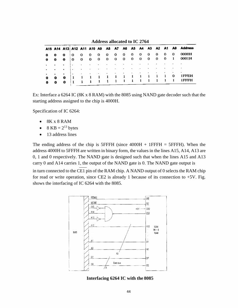
Ex: Interface a 6264 IC (8K x 8 RAM) with the 8085 using NAND gate decoder such that the
starting address assigned to the chip is 4000H.
Specification of IC 6264:
8K x 8 RAM
8 KB = 213 bytes
13 address lines
The ending address of the chip is 5FFFH (since 4000H + 1FFFH = 5FFFH). When the
address 4000H to 5FFFH are written in binary form, the values in the lines A15, A14, A13 are
0, 1 and 0 respectively. The NAND gate is designed such that when the lines A15 and A13
carry 0 and A14 carries 1, the output of the NAND gate is 0. The NAND gate output is
in turn connected to the CE1 pin of the RAM chip. A NAND output of 0 selects the RAM chip
for read or write operation, since CE2 is already 1 because of its connection to +5V. Fig.
shows the interfacing of IC 6264 with the 8085.
Interfacing 6264 IC with the 8085
45
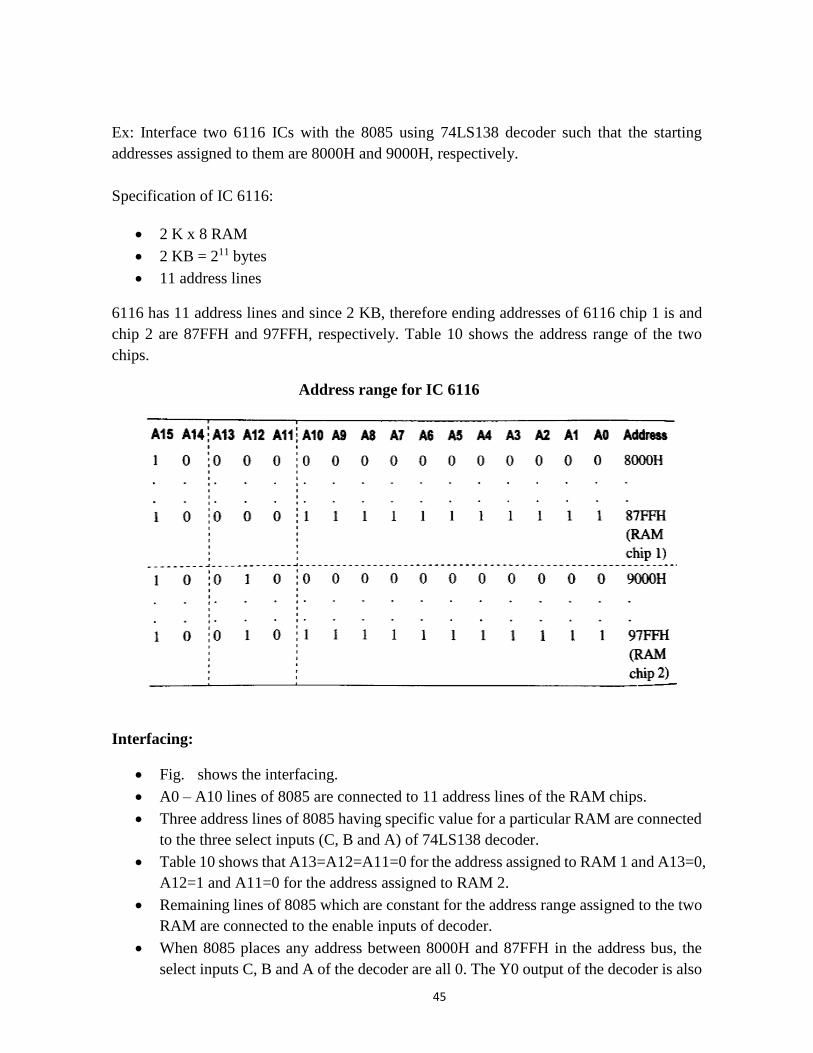
Ex: Interface two 6116 ICs with the 8085 using 74LS138 decoder such that the starting
addresses assigned to them are 8000H and 9000H, respectively.
Specification of IC 6116:
2 K x 8 RAM
2 KB = 211 bytes
11 address lines
6116 has 11 address lines and since 2 KB, therefore ending addresses of 6116 chip 1 is and
chip 2 are 87FFH and 97FFH, respectively. Table 10 shows the address range of the two
chips.
Address range for IC 6116
Interfacing:
Fig. shows the interfacing.
A0 – A10 lines of 8085 are connected to 11 address lines of the RAM chips.
Three address lines of 8085 having specific value for a particular RAM are connected
to the three select inputs (C, B and A) of 74LS138 decoder.
Table 10 shows that A13=A12=A11=0 for the address assigned to RAM 1 and A13=0,
A12=1 and A11=0 for the address assigned to RAM 2.
Remaining lines of 8085 which are constant for the address range assigned to the two
RAM are connected to the enable inputs of decoder.
When 8085 places any address between 8000H and 87FFH in the address bus, the
select inputs C, B and A of the decoder are all 0. The Y0 output of the decoder is also

46
0, selecting RAM 1.
When 8085 places any address between 9000H and 97FFH in the address bus, the
select inputs C, B and A of the decoder are 0, 1 and 0. The Y2 output of the decoder is
also 0, selecting RAM 2.
Peripheral Mapped I/O Interfacing
In this method, the I/O devices are treated differently from memory chips. The control signals
I/O read ( I͞͞͞͞ O͞͞ R͞͞͞͞ ) and I/O write ( I͞͞ O͞͞ W͞͞ ), which are derived from the IO/M͞͞ , ͞͞R͞͞ D͞͞ and W͞͞ R͞͞ signals
of the 8085, are used to activate input and output devices, respectively. Generation of these
control signals is shown in Fig. and Table shows the status of IO/M͞͞ , ͞͞R͞͞ D͞͞ and W͞͞ R͞͞ signals
during I/O read and I/O write operation.
Fig. Generation of IOR and IOW signals
IN instruction is used to access input device and OUT instruction is used to access output
device. Each I/O device is identified by a unique 8-bit address assigned to it. Since the control
signals used to access input and output devices are different, and all I/O device use 8-bit
address, a maximum of 256 (28) input devices and 256 output devices can be interfaced with
8085.
Status of IOR and IOW signals in 8085.
IO/M
RD
WR
IOR
IOW Operation
1 0 1 0 1 I/O read operation
1 1 0 1 0 I/O write operation
0 X X 1 1 Memory read or write operation
Ex: Interface an 8-bit DIP switch with the 8085 such that the address assigned to the DIP
switch if F0H.
IN instruction is used to get data from DIP switch and store it in accumulator. Steps involved

47
in the execution of this instruction are:
i. Address F0H is placed in the lines A0 – A7 and a copy of it in lines A8 – A15.
ii. The IOR signal is activated ( IOR = 0), which makes the selected input device to place
its data in the data bus.
iii. The data in the data bus is read and store in the accumulator.
A7 A6 A5 A4 A3 A2 A1 A0
1 1 1 1 0 0 0 0 = F0H
A0 – A7 lines are connected to a NAND gate decoder such that the output of NAND gate is
0. The output of NAND gate is ORed with the IOR signal and the output of OR gate is
connected to 1G and 2G of the 74LS244. When 74LS244 is enabled, data from the DIP switch
is placed on the data bus of the 8085. The 8085 read data and store in the
accumulator. Thus data from DIP switch is transferred to the accumulator.
Memory Mapped I/O Interfacing
In memory-mapped I/O, each input or output device is treated as if it is a memory location.
The MEMR and MEMW control signals are used to activate the devices. Each input or output
device is identified by unique 16-bit address, similar to 16-bit address assigned to
memory location. All memory related instruction like LDA 2000H, LDAX B, MOV A, M
can be used. Since the I/O devices use some of the memory address space of 8085, the maximum memory
capacity is lesser than 64 KB in this method.
Ex: Interface an 8-bit DIP switch with the 8085 using logic gates such that the address
assigned to it is F0F0H.
Since a 16-bit address has to be assigned to a DIP switch, the memory-mapped I/O technique
must be used. Using LDA F0F0H instruction, the data from the 8-bit DIP switch can be
transferred to the accumulator. The steps involved are:
i. The address F0F0H is placed in the address bus A0 – A15.
ii. The MEMR signal is made low for some time.
iii. The data in the data bus is read and stored in the accumulator.
Fig. shows the interfacing diagram.
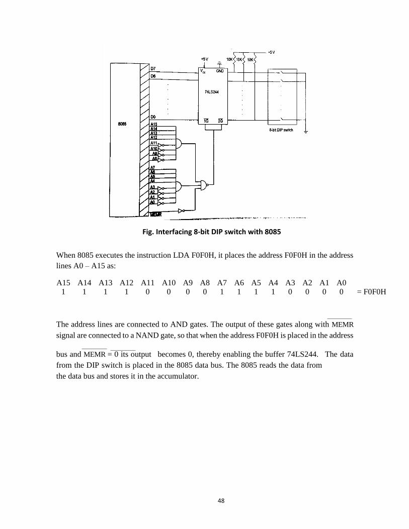
48
Fig. Interfacing 8-bit DIP switch with 8085
When 8085 executes the instruction LDA F0F0H, it places the address F0F0H in the address
lines A0 – A15 as:
A15 A14 A13 A12 A11 A10 A9 A8 A7 A6 A5 A4 A3 A2 A1 A0
1 1 1 1 0 0 0 0 1 1 1 1 0 0 0 0 = F0F0H
The address lines are connected to AND gates. The output of these gates along with MEMR
signal are connected to a NAND gate, so that when the address F0F0H is placed in the address
bus and MEMR = 0 its output becomes 0, thereby enabling the buffer 74LS244. The data
from the DIP switch is placed in the 8085 data bus. The 8085 reads the data from
the data bus and stores it in the accumulator.

49
Mode of Transfer:
The binary information that is received from an external device is usually stored in the
memory unit. The information that is transferred from the CPU to the external device is
originated from the memory unit. CPU merely processes the information but the source
and target is always the memory unit. Data transfer between CPU and the I/O devices
may be done in different modes.
Data transfer to and from the peripherals may be done in any of the three possible ways
1. Programmed I/O.
2. Interrupt- initiated I/O.
3. Direct Memory Access ( DMA).
Now let’s discuss each mode one by one.
1. Programmed I/O: It is due to the result of the I/O instructions that are written
in the computer program. Each data item transfer is initiated by an instruction in
the program. Usually the transfer is from a CPU register and memory. In this
case it requires constant monitoring by the CPU of the peripheral devices.
Example of Programmed I/O: In this case, the I/O device does not have direct
access to the memory unit. A transfer from I/O device to memory requires the
execution of several instructions by the CPU, including an input instruction to
transfer the data from device to the CPU and store instruction to transfer the data
from CPU to memory. In programmed I/O, the CPU stays in the program loop
until the I/O unit indicates that it is ready for data transfer. This is a time
consuming process since it needlessly keeps the CPU busy. This situation can be
avoided by using an interrupt facility. This is discussed below.
2. Interrupt- initiated I/O: Since in the above case we saw the CPU is kept busy
unnecessarily. This situation can very well be avoided by using an interrupt
driven method for data transfer. By using interrupt facility and special commands
to inform the interface to issue an interrupt request signal whenever data is
available from any device. In the meantime the CPU can proceed for any other
program execution. The interface meanwhile keeps monitoring the device.
Whenever it is determined that the device is ready for data transfer it initiates an
interrupt request signal to the computer. Upon detection of an external interrupt
signal the CPU stops momentarily the task that it was already performing,
branches to the service program to process the I/O transfer, and then return to the
task it was originally performing.
3. Direct Memory Access: The data transfer between a fast storage media such as
magnetic disk and memory unit is limited by the speed of the CPU. Thus we can
allow the peripherals directly communicate with each other using the memory
buses, removing the intervention of the CPU. This type of data transfer technique
is known as DMA or direct memory access. During DMA the CPU is idle and it

50
has no control over the memory buses. The DMA controller takes over the buses
to manage the transfer directly between the I/O devices and the memory unit.
Bus Request: It is used by the DMA controller to request the CPU to relinquish the
control of the buses.
Bus Grant: It is activated by the CPU to Inform the external DMA controller that the
buses are in high impedance state and the requesting DMA can take control of the
buses. Once the DMA has taken the control of the buses it transfers the data. This
transfer can take place in many ways.
Example it can transfer using
Bus Transfer: In which a block sequence consisting of memory words is transferred
in a continuous burst where the DMA controller is the master of the memory buses.
This mode is needed for fast devices like magnetic disks.
Cyclic Stealing: In this DMA controller transfers one word at a time after which it
must return the control of the buses to the CPU. The CPU merely delays its operation
for one memory cycle to allow the direct memory I/O transfer to “steal” one memory
cycle.
51
Chapter 6
Interrupt
In system programming, an interrupt is a signal to the processor emitted by hardware or
software indicating an event that needs immediate attention. An interrupt alerts the
processor to a high-priority condition requiring the interruption of the current code the
processor is executing. The processor responds by suspending its current activities,
saving its state, and executing a function called an interrupt handler (or an interrupt
service routine, ISR) to deal with the event. This interruption is temporary, and, after the
interrupt handler finishes, the processor resumes normal activities.
There are two types of interrupts: hardware interrupts and software interrupts.
Hardware interrupts are used by devices to communicate that they require attention
from the operating system. Internally, hardware interrupts are implemented using
electronic alerting signals that are sent to the processor from an external device, which is
either a part of the computer itself, such as a disk controller, or an external peripheral.
For example, pressing a key on the keyboard or moving the mouse triggers hardware
interrupts that cause the processor to read the keystroke or mouse position. Unlike the
software type (described below), hardware interrupts are asynchronous and can occur in
the middle of instruction execution, requiring additional care in programming. The act
of initiating a hardware interrupt is referred to as an interrupt request (IRQ).
Software interrupt is caused either by an exceptional condition in the processor itself,
or a special instruction in the instruction set which causes an interrupt when it is
executed. The former is often called a trap or exception and is used for errors or events
occurring during program executions that are exceptional enough that they cannot be
handled within the program itself. For example, a divide-by-zero exception will be
thrown if the processor's arithmetic logic unit is commanded to divide a number by zero
as this instruction is an error and impossible. The operating system will catch this
exception, and can choose to abort the instruction. Software interrupt instructions can
function similarly to subroutine calls and are used for a variety of purposes, such as to
request services from device drivers, like interrupts sent to and from a disk controller to
request reading or writing of data to and from the disk.
Each interrupt has its own interrupt handler. The number of hardware interrupts is
limited by the number of interrupt request (IRQ) lines to the processor, but there may be
hundreds of different software interrupts. Interrupts are a commonly used technique for
computer multitasking, especially in real-time computing. Such a system is said to be
interrupt-driven.[3]
Interrupts are similar to signals, the difference being that signals are used for IPC,
mediated by the kernel (possibly via system calls) and handled by processes, while
interrupts are mediated by the processor and handled by the kernel. The kernel may pass
an interrupt as a signal to the process that caused it (typical examples are SIGSEGV,
SIGBUS, SIGILL and SIGFPE).
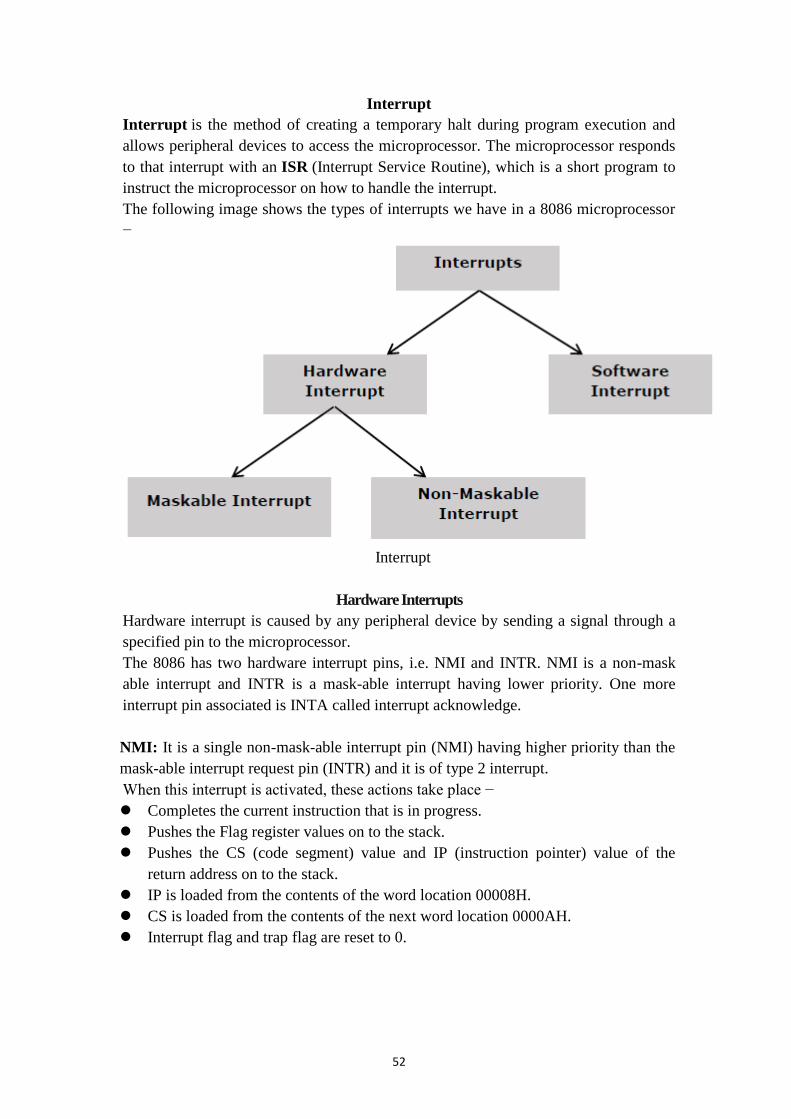
52
Interrupt
Interrupt is the method of creating a temporary halt during program execution and
allows peripheral devices to access the microprocessor. The microprocessor responds
to that interrupt with an ISR (Interrupt Service Routine), which is a short program to
instruct the microprocessor on how to handle the interrupt.
The following image shows the types of interrupts we have in a 8086 microprocessor
−
Interrupt
Hardware Interrupts
Hardware interrupt is caused by any peripheral device by sending a signal through a
specified pin to the microprocessor.
The 8086 has two hardware interrupt pins, i.e. NMI and INTR. NMI is a non-mask
able interrupt and INTR is a mask-able interrupt having lower priority. One more
interrupt pin associated is INTA called interrupt acknowledge.
NMI: It is a single non-mask-able interrupt pin (NMI) having higher priority than the
mask-able interrupt request pin (INTR) and it is of type 2 interrupt.
When this interrupt is activated, these actions take place −
Completes the current instruction that is in progress.
Pushes the Flag register values on to the stack.
Pushes the CS (code segment) value and IP (instruction pointer) value of the
return address on to the stack.
IP is loaded from the contents of the word location 00008H.
CS is loaded from the contents of the next word location 0000AH.
Interrupt flag and trap flag are reset to 0.
53
INTR: The INTR is a mask-able interrupt because the microprocessor will be
interrupted only if interrupts are enabled using set interrupt flag instruction. It should
not be enabled using clear interrupt Flag instruction.
The INTR interrupt is activated by an I/O port. If the interrupt is enabled and NMI is
disabled, then the microprocessor first completes the current execution and sends ‘0’
on INTA pin twice. The first ‘0’ means INTA informs the external device to get ready
and during the second ‘0’ the microprocessor receives the 8 bit, say X, from the
programmable interrupt controller.
These actions are taken by the microprocessor −
First completes the current instruction.
Activates INTA output and receives the interrupt type, say X.
Flag register value; CS value of the return address and IP value of the return
address are pushed on to the stack.
IP value is loaded from the contents of word location X × 4
CS is loaded from the contents of the next word location.
Interrupt flag and trap flag is reset to 0
Software Interrupts
Some instructions are inserted at the desired position into the program to create
interrupts. These interrupt instructions can be used to test the working of various
interrupt handlers. It includes –
INT- Interrupt instruction with type number
It is 2-byte instruction. First byte provides the op-code and the second byte provides
the interrupt type number. There are 256 interrupt types under this group.
Its execution includes the following steps −
Flag register value is pushed on to the stack.
CS value of the return address and IP value of the return address are pushed on to
the stack.
IP is loaded from the contents of the word location ‘type number’× 4.
CS is loaded from the contents of the next word location.
Interrupt Flag and Trap Flag are reset to 0
The starting address for type0 interrupt is 000000H, for type1 interrupt is 00004H
similarly for type2 is 00008H and ……so on. The first five pointers are dedicated
interrupt pointers. i.e. -
TYPE 0 interrupt represents division by zero situation.
TYPE 1 interrupt represents single-step execution during the debugging of a
program.
TYPE 2 interrupt represents non-mask-able NMI interrupt.
TYPE 3 interrupt represents break-point interrupt.
TYPE 4 interrupt represents overflow interrupt.

54
The interrupts from Type 5 to Type 31 are reserved for other advanced
microprocessors, and interrupts from 32 to Type 255 are available for hardware and
software interrupts.
INT 3-Break Point Interrupt Instruction
It is a 1-byte instruction having op-code is CCH. These instructions are inserted into
the program so that when the processor reaches there, then it stops the normal
execution of program and follows the break-point procedure.
Its execution includes the following steps −
Flag register value is pushed on to the stack.
CS value of the return address and IP value of the return address are pushed on to
the stack.
IP is loaded from the contents of the word location 3×4 = 0000CH
CS is loaded from the contents of the next word location.
Interrupt Flag and Trap Flag are reset to 0.
INTO - Interrupt on overflow instruction
It is a 1-byte instruction and their mnemonic INTO. The op-code for this instruction
is CEH. As the name suggests it is a conditional interrupt instruction, i.e. it is active
only when the overflow flag is set to 1 and branches to the interrupt handler whose
interrupt type number is 4. If the overflow flag is reset then, the execution continues
to the next instruction.
Its execution includes the following steps −
Flag register values are pushed on to the stack.
CS value of the return address and IP value of the return address are pushed on to
the stack.
IP is loaded from the contents of word location 4×4 = 00010H
CS is loaded from the contents of the next word location.
Interrupt flag and Trap flag are reset to 0
Non-Mask-Able Interrupts
A non-mask-able interrupt (NMI) is a type of hardware interrupt (or signal to the
processor) that prioritizes a certain thread or process. Unlike other types of interrupts,
the non-mask-able interrupt cannot be ignored through the use of interrupt masking
techniques.
Mask-Able interrupt
An Interrupt that can be disabled or ignored by the instructions of CPU is called as
mask-able Interrupt.
Eg: RST6.5, RST7.5, RST5.5 OF 8085 is mask-able Interrupts.

55
Chapter 7
Data transfer Techniques
Programmed input/output (PIO) is a method of transferring data between
the CPU and a peripheral, such as a network adapter or an ATA storage device.
For programmed I/O, the software that is running on the CPU uses instructions to
perform data transfers to or from an I/O device. This is in contrast to Direct Memory
Access (DMA) transfers. The term Programmed I/O can refer to either MMIO or
PMIO. Port-mapped I/O (PMIO) refers to a special address space outside of normal
memory that is accessed with instructions such as IN and OUT. Memory-mapped
I/O[1] (MMIO) refers to I/O devices being allocated addresses inside the normal Von
Neumann address space that is primarily used for program and data. Such I/O is done
using instructions such as LOAD and STORE. PMIO was very useful for early
microprocessors with small address spaces, since the valuable resource was not
consumed by the I/O devices.
The best known example of a PC device that uses programmed I/O is
the ATA interface; however, this interface can also be operated in any of
several DMA modes. Many older devices in a PC also use PIO, including legacy serial
ports, legacy parallel ports when not in ECP mode, the PS/2 keyboard and mouse ports,
legacy MIDI and joystick ports, the interval timer, and older network interfaces.
Synchronous data transmission
Synchronous transmission is transmission of signals in a fixed interval based on a
predefined clocking signal and is meant for constant and reliable transmission of
time-sensitive data such as VoIP and audio/video streaming.
This method of transmission is used when large amounts of data need to be transferred
quickly since data is transferred in large blocks instead of individual characters. The
data blocks are spaced and grouped in regular intervals and preceded by synchronous
characters that a remote device decode and use to synchronize the connection between
the end points.
After synchronization is complete, the transmission can begin.
Asynchronous data transfer
The transmission of asynchronous data is not prompted by a clock signal when sending
the data to the receiver, unlike in synchronous methods, where sending data is
measured against a time reference. Compared to synchronous transmission,
asynchronous communication has a few advantages:
It is more flexible and devices can exchange information at their own pace.
Individual data characters can complete themselves so that even if one packet is
corrupted, its predecessors and successors will not be affected.
It does not require complex processes by the receiving device. This means that
an inconsistency in the transmission of data does not result in a big crisis, since
the device can keep up with the data stream. This also makes asynchronous

56
transfers suitable for applications where character data is generated in an
irregular manner.
There are also some disadvantages of using asynchronous data for transmission:
The success of these transmissions depends on the start bits and their
recognition. This can be easily susceptible to line interference, causing these
bits to be corrupted or distorted.
A large portion of the transmitted data is used for control and identification bits
for headers and thus carries no useful information related to the transmitted
data. This invariably means that more data packets need to be sent.
Interrupt driven I/O
Interrupt driven I/O is an alternative scheme dealing with I/O. Interrupt I/O is a way of
controlling input/output activity whereby a peripheral or terminal that needs to make
or receive a data transfer sends a signal. This will cause a program interrupt to be set.
At a time appropriate to the priority level of the I/O interrupt. Relative to the total
interrupt system, the processors enter an interrupt service routine. The function of the
routine will depend upon the system of interrupt levels and priorities that is
implemented in the processor. The interrupt technique requires more complex
hardware and software, but makes far more efficient use of the computer’s time and
capacities
For input, the device interrupts the CPU when new data has arrived and is ready to be
retrieved by the system processor. The actual actions to perform depend on whether the
device uses I/O ports or memory mapping.
For output, the device delivers an interrupt either when it is ready to accept new data
or to acknowledge a successful data transfer. Memory-mapped and DMA-capable
devices usually generate interrupts to tell the system they are done with the buffer.
Here the CPU works on its given tasks continuously. When an input is available, such
as when someone types a key on the keyboard, then the CPU is interrupted from its
work to take care of the input data. The CPU can work continuously on a task without
checking the input devices, allowing the devices themselves to interrupt it as
necessary.
Direct Memory Access
Direct memory access (DMA) is a feature of computer systems that allows certain
hardware subsystems to access main system memory (Random-access memory),
independent of the central processing unit (CPU).
Without DMA, when the CPU is using programmed input/output, it is typically fully
occupied for the entire duration of the read or write operation, and is thus unavailable
to perform other work. With DMA, the CPU first initiates the transfer, then it does
other operations while the transfer is in progress, and it finally receives
an interrupt from the DMA controller when the operation is done. This feature is useful
at any time that the CPU cannot keep up with the rate of data transfer, or when the
CPU needs to perform work while waiting for a relatively slow I/O data transfer. Many
hardware systems use DMA, including disk drivecontrollers, graphics cards, network
cards and sound cards. DMA is also used for intra-chip data transfer in multi-core

57
processors. Computers that have DMA channels can transfer data to and from devices
with much less CPU overhead than computers without DMA channels. Similarly, a
processing element inside a mufti-core processor can transfer data to and from its local
memory without occupying its processor time, allowing computation and data transfer
to proceed in parallel.
DMA can also be used for "memory to memory" copying or moving of data within
memory. DMA can offload expensive memory operations, such as large copies
or scatter-gather operations, from the CPU to a dedicated DMA engine. An
implementation example is the I/O Acceleration Technology.
Serial I/O
Serial input/output (SIO) A method of communicating data between devices,
typically a computer and its peripherals, the individual data bits being sent
sequentially. Serial communication may be asynchronous, where the data characters
include start and stop bits to delimit the data, or synchronous, where such additional
bits are omitted and the delimiting of the data depends purely on timing.
Asynchronous serial communication is more flexible whereas synchronous serial
communication makes better use of the available bandwidth. Asynchronous methods
are generally used with dial-up modems or for general connection of simple serial
peripherals. Synchronous methods are usually to be found where leased lines or
proprietary interfaces are used.
Until recently SIO was a relatively slow mode, but advances in silicon technology
means that very fast SIO (hundreds of megabits per second) now make SIO a very
cost-effective alternative to parallel interfaces. See USB, Firewire, serial IDE.
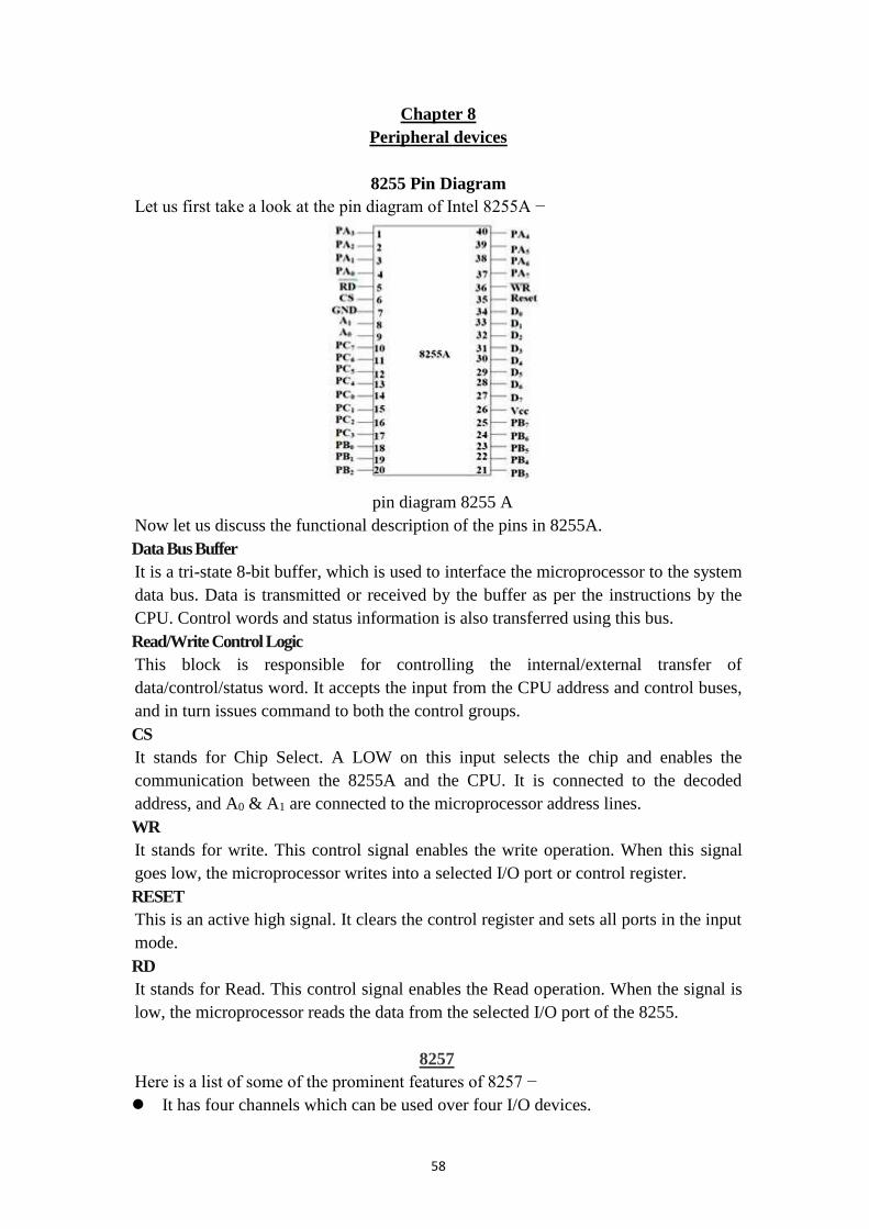
58
Chapter 8
Peripheral devices
8255 Pin Diagram
Let us first take a look at the pin diagram of Intel 8255A −
pin diagram 8255 A
Now let us discuss the functional description of the pins in 8255A.
Data Bus Buffer
It is a tri-state 8-bit buffer, which is used to interface the microprocessor to the system
data bus. Data is transmitted or received by the buffer as per the instructions by the
CPU. Control words and status information is also transferred using this bus.
Read/Write Control Logic
This block is responsible for controlling the internal/external transfer of
data/control/status word. It accepts the input from the CPU address and control buses,
and in turn issues command to both the control groups.
CS
It stands for Chip Select. A LOW on this input selects the chip and enables the
communication between the 8255A and the CPU. It is connected to the decoded
address, and A0 & A1 are connected to the microprocessor address lines.
WR
It stands for write. This control signal enables the write operation. When this signal
goes low, the microprocessor writes into a selected I/O port or control register.
RESET
This is an active high signal. It clears the control register and sets all ports in the input
mode.
RD
It stands for Read. This control signal enables the Read operation. When the signal is
low, the microprocessor reads the data from the selected I/O port of the 8255.
8257
Here is a list of some of the prominent features of 8257 −
It has four channels which can be used over four I/O devices.

59
Each channel has 16-bit address and 14-bit counter.
Each channel can transfer data up to 64kb.
Each channel can be programmed independently.
Each channel can perform read transfer, write transfer and verify transfer
operations.
It generates MARK signal to the peripheral device that 128 bytes have been
transferred.
It requires a single phase clock.
Its frequency ranges from 250Hz to 3MHz.
It operates in 2 modes, i.e., Master mode and Slave mode.
8257 Architecture
The following image shows the architecture of 8257 −
Pin diagram of 8257

60
8257 Pin Description
The following image shows the pin diagram of a 8257 DMA controller −
8257 pin description
DRQ0−DRQ3
These are the four individual channel DMA request inputs, which are used by the
peripheral devices for using DMA services. When the fixed priority mode is selected,
then DRQ0 has the highest priority and DRQ3 has the lowest priority among them.
DACKo − DACK3
These are the active-low DMA acknowledge lines, which updates the requesting
peripheral about the status of their request by the CPU. These lines can also act as
strobe lines for the requesting devices.
Do − D7
These are bidirectional, data lines which are used to interface the system bus with the
internal data bus of DMA controller. In the Slave mode, it carries command words to
8257 and status word from 8257. In the master mode, these lines are used to send
higher byte of the generated address to the latch. This address is further latched using
ADSTB signal.
IOR
It is an active-low bidirectional tri-state input line, which is used by the CPU to read
internal registers of 8257 in the Slave mode. In the master mode, it is used to read data
from the peripheral devices during a memory write cycle.
IOW
It is an active low bi-direction tri-state line, which is used to load the contents of the
data bus to the 8-bit mode register or upper/lower byte of a 16-bit DMA address
register or terminal count register. In the master mode, it is used to load the data to the
peripheral devices during DMA memory read cycle.
CLK
It is a clock frequency signal which is required for the internal operation of 8257.
RESET
This signal is used to RESET the DMA controller by disabling all the DMA channels.
61
Ao - A3
These are the four least significant address lines. In the slave mode, they act as an
input, which selects one of the registers to be read or written. In the master mode, they
are the four least significant memory address output lines generated by 8257.
CS
It is an active-low chip select line. In the Slave mode, it enables the read/write
operations to/from 8257. In the master mode, it disables the read/write operations
to/from 8257.
A4 - A7
These are the higher nibble of the lower byte address generated by DMA in the master
mode.
READY
It is an active-high asynchronous input signal, which makes DMA ready by inserting
wait states.
HRQ
This signal is used to receive the hold request signal from the output device. In the
slave mode, it is connected with a DRQ input line 8257. In Master mode, it is
connected with HOLD input of the CPU.
HLDA
It is the hold acknowledgement signal which indicates the DMA controller that the
bus has been granted to the requesting peripheral by the CPU when it is set to 1.
MEMR
It is the low memory read signal, which is used to read the data from the addressed
memory locations during DMA read cycles.
MEMW
It is the active-low three state signal which is used to write the data to the addressed
memory location during DMA write operation.
ADST
This signal is used to convert the higher byte of the memory address generated by the
DMA controller into the latches.
AEN
This signal is used to disable the address bus/data bus.
TC
It stands for ‘Terminal Count’, which indicates the present DMA cycle to the present
peripheral devices.
MARK
The mark will be activated after each 128 cycles or integral multiples of it from the
beginning. It indicates the current DMA cycle is the 128th cycle since the previous
MARK output to the selected peripheral device.
V cc
It is the power signal which is required for the operation of the circuit.
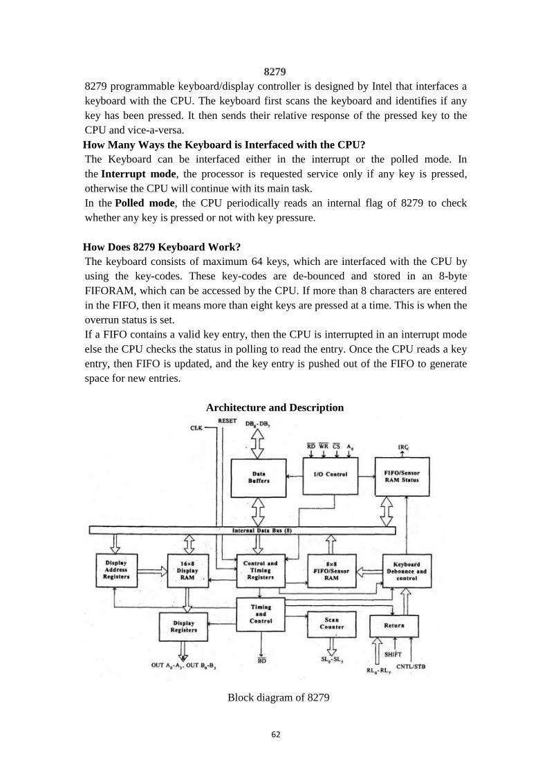
62
8279
8279 programmable keyboard/display controller is designed by Intel that interfaces a
keyboard with the CPU. The keyboard first scans the keyboard and identifies if any
key has been pressed. It then sends their relative response of the pressed key to the
CPU and vice-a-versa.
How Many Ways the Keyboard is Interfaced with the CPU?
The Keyboard can be interfaced either in the interrupt or the polled mode. In
the Interrupt mode, the processor is requested service only if any key is pressed,
otherwise the CPU will continue with its main task.
In the Polled mode, the CPU periodically reads an internal flag of 8279 to check
whether any key is pressed or not with key pressure.
How Does 8279 Keyboard Work?
The keyboard consists of maximum 64 keys, which are interfaced with the CPU by
using the key-codes. These key-codes are de-bounced and stored in an 8-byte
FIFORAM, which can be accessed by the CPU. If more than 8 characters are entered
in the FIFO, then it means more than eight keys are pressed at a time. This is when the
overrun status is set.
If a FIFO contains a valid key entry, then the CPU is interrupted in an interrupt mode
else the CPU checks the status in polling to read the entry. Once the CPU reads a key
entry, then FIFO is updated, and the key entry is pushed out of the FIFO to generate
space for new entries.
Architecture and Description
Block diagram of 8279
63
I/O Control and Data Buffer
This unit controls the flow of data through the microprocessor. It is enabled only
when D is low. Its data buffer interfaces the external bus of the system with the
internal bus of the microprocessor. The pins A0, RD, and WR are used for command,
status or data read/write operations.
Control and Timing Register and Timing Control
This unit contains registers to store the keyboard, display modes, and other operations
as programmed by the CPU. The timing and control unit handles the timings for the
operation of the circuit.
Scan Counter
It has two modes i.e. Encoded mode and Decoded mode. In the encoded mode, the
counter provides the binary count that is to be externally decoded to provide the scan
lines for the keyboard and display.
In the decoded scan mode, the counter internally decodes the least significant 2 bits
and provides a decoded 1 out of 4 scan on SL0-SL3.
Return Buffers, Keyboard Debounce, and Control
This unit first scans the key closure row-wise, if found then the keyboard debounce
unit debounces the key entry. In case, the same key is detected, then the code of that
key is directly transferred to the sensor RAM along with SHIFT & CONTROL key
status.
FIFO/Sensor RAM and Status Logic
This unit acts as 8-byte first-in-first-out (FIFO) RAM where the key code of every
pressed key is entered into the RAM as per their sequence. The status logic generates
an interrupt request after each FIFO read operation till the FIFO gets empty.
In the scanned sensor matrix mode, this unit acts as sensor RAM where its each row is
loaded with the status of their corresponding row of sensors into the matrix. When the
sensor changes its state, the IRQ line changes to high and interrupts the CPU.
Display Address Registers and Display RAM
This unit consists of display address registers which holds the addresses of the word
currently read/written by the CPU to/from the display RAM.
8279 − Pin Description
The following figure shows the pin diagram of 8279 −
Data Bus Lines, DB0 - DB7
These are 8 bidirectional data bus lines used to transfer the data to/from the CPU.
CLK
The clock input is used to generate internal timings required by the microprocessor.
64
RESET
As the name suggests this pin is used to reset the microprocessor.
CS Chip Select
When this pin is set to low, it allows read/write operations, else this pin should be set
to high.
A0
This pin indicates the transfer of command/status information. When it is low, it
indicates the transfer of data.
RD, WR
This Read/Write pin enables the data buffer to send/receive data over the data bus.
IRQ
This interrupt output line goes high when there is data in the FIFO sensor RAM. The
interrupt line goes low with each FIFO RAM read operation. However, if the FIFO
RAM further contains any key-code entry to be read by the CPU, this pin again goes
high to generate an interrupt to the CPU.
Vss, V cc
These are the ground and power supply lines of the microprocessor.
SL0 − SL3
These are the scan lines used to scan the keyboard matrix and display the digits. These
lines can be programmed as encoded or decoded, using the mode control register.
RL0 − RL7
These are the Return Lines which are connected to one terminal of keys, while the
other terminal of the keys is connected to the decoded scan lines. These lines are set to
0 when any key is pressed.
SHIFT
The Shift input line status is stored along with every key code in FIFO in the scanned
keyboard mode. Till it is pulled low with a key closure, it is pulled up internally to
keep it high
CNTL/STB - CONTROL/STROBED I/P Mode
In the keyboard mode, this line is used as a control input and stored in FIFO on a key
closure. The line is a strobe line that enters the data into FIFO RAM, in the strobed
input mode. It has an internal pull up. The line is pulled down with a key closure.
BD
It stands for blank display. It is used to blank the display during digit switching.
OUTA0 – OUTA3 and OUTB0 – OUTB3
These are the output ports for two 16x4 or one 16x8 internal display refresh registers.
The data from these lines is synchronized with the scan lines to scan the display and
the keyboard.
Operational Modes of 8279
65
There are two modes of operation on 8279 − Input Mode and Output Mode.
Input Mode
This mode deals with the input given by the keyboard and this mode is further classified
into 3 modes.
Scanned Keyboard Mode − In this mode, the key matrix can be interfaced using
either encoded or decoded scans. In the encoded scan, an 8×8 keyboard or in the
decoded scan, a 4×8 keyboard can be interfaced. The code of key pressed with
SHIFT and CONTROL status is stored into the FIFO RAM.
Scanned Sensor Matrix − In this mode, a sensor array can be interfaced with the
processor using either encoder or decoder scans. In the encoder scan, 8×8 sensor
matrix or with decoder scan 4×8 sensor matrix can be interfaced.
Strobed Input − In this mode, when the control line is set to 0, the data on the
return lines is stored in the FIFO byte by byte.
Output Mode
This mode deals with display-related operations. This mode is further classified into
two output modes.
Display Scan − This mode allows 8/16 character multiplexed displays to be
organized as dual 4-bit/single 8-bit display units.
Display Entry − This mode allows the data to be entered for display either from the
right side/left side.


![Ece Vi Microprocessors [10ec62] Notes](https://img.pdfslide.us/doc/110x75/55cf99ba550346d0339ee2ed/ece-vi-microprocessors-10ec62-notes.jpg)