Embed Size (px)
Citation preview

MICROPROCESSOR & MICROCONTROLLER
LABORATORY MANUAL
4TH SEMESTER ISE
SUBJECT CODE: 15CSL48
FACULTY: MRS DEEPTI C
DEPARTMENT OF
INFORMATION SCIENCE AND
ENGINEERING
PESIT – BANGALORE SOUTH CAMPUS
1KM BEFORE ELECTRONICS CITY,
HOSUR ROAD, BANGALORE-560100.

PESIT BANGALORE SOUTH CAMPUS DEPARTMENT OF ISE
4T H SEMESTER MICROPROCESSOR LAB 10CSL48 Page 2
MICROPROCESSOR AND MICROCONTROLLER
LABORATORY [As per Choice Based Credit System (CBCS) scheme]
(Effective from the academic year 2016 -2017)
SEMESTER – IV
Subject Code 15CSL48 IA Marks 20
Number of Lecture Hours/Week 01I + 02 P Exam Marks 80
Total Number of Lecture Hours 40 Exam Hours 03 Credits – 02
Course objectives: This course will enable students to
· To provide practical exposure to the students on microprocessors, design and coding
knowledge on 80x86 family/ARM. To give the knowledge and practical exposure on
connectivity and execute of interfacing devices with 8086/ARM kit like LED displays,
Keyboards, DAC/ADC, and various other devices.
Description
Demonstration and Explanation hardware components and Faculty in-charge should
explain 8086architecture, pin diagram in one slot. The second slot, the Faculty in-charge
should explain instruction set types/category etc.
Students have to prepare a write-up on the same and include it in the Lab record and to be
evaluated.
Laboratory Session-1: Write-up on Microprocessors, 8086 Functional block diagram, Pin
diagram and description. The same information is also taught in theory class; this helps the
students to understand better.
Laboratory Session-2: Write-up on Instruction group, Timing diagrams, etc. The same
information is also taught in theory class; this helps the students to understand better.
Note: These TWO Laboratory sessions are used to fill the gap between theory classes and
practical sessions. Both sessions are evaluated as lab experiments for 20 marks.
Experiments
· Develop and execute the following programs using 8086 Assembly Language. Any
suitable assembler like MASM/TASM/8086 kit or any equivalent software may be used.
· Program should have suitable comments.
· The board layout and the circuit diagram of the interface are to be provided to the student
during the examination.
· Software Required: Open source ARM Development platform, KEIL IDE and Proteus for
Simulation

PESIT BANGALORE SOUTH CAMPUS DEPARTMENT OF ISE
4T H SEMESTER MICROPROCESSOR LAB 10CSL48 Page 3
SOFTWARE PROGRAMS: PART A
1. Design and develop an assembly language program to search a
key element “X” in a list of „n‟16-bit numbers. Adopt Binary search
algorithm in your program for searching.
2. Design and develop an assembly program to sort a given set of
„n‟ 16-bit numbers in ascending order. Adopt Bubble Sort algorithm
to sort given elements.
3. Develop an assembly language program to reverse a given string
and verify whether it is a palindrome or not. Display the appropriate
message.
4. Develop an assembly language program to compute nCr using
recursive procedure. Assume that „n‟ and „r‟ are non-negative
integers.
5. Design and develop an assembly language program to read the
current time and Date from the system and display it in the standard
format on the screen.
6. To write and simulate ARM assembly language programs for data
transfer, arithmetic and logical operations (Demonstrate with the
help of a suitable program).
7. To write and simulate C Programs for ARM microprocessor
using KEIL (Demonstrate with the help of a suitable program)
Note: To use KEIL one may refer the book: Insider‟s Guide to the
ARM7 based microcontrollers, Hitex Ltd., 1st edition, 2005

PESIT BANGALORE SOUTH CAMPUS DEPARTMENT OF ISE
4T H SEMESTER MICROPROCESSOR LAB 10CSL48 Page 4
HARDWARE PROGRAMS: PART B
8. a. Design and develop an assembly program to demonstrate BCD
Up-Down Counter (00-99) on the Logic Controller Interface.
b. Design and develop an assembly program to read the status of
two 8-bit inputs (X & Y) from the Logic Controller Interface and
display X*Y.
9. Design and develop an assembly program to display messages
“FIRE” and “HELP” alternately with flickering effects on a 7-
segment display interface for a suitable period of time. Ensure a
flashing rate that makes it easy to read both the messages (Examiner
does not specify these delay values nor is it necessary for the student
to compute these values).
10. Design and develop an assembly program to drive a Stepper
Motor interface and rotate the motor in specified direction
(clockwise or counter-clockwise) by N steps (Direction and N are
specified by the examiner). Introduce suitable delay between
successive steps. (Any arbitrary value for the delay may be assumed
by the student).
11. Design and develop an assembly language program to
a. Generate the Sine Wave using DAC interface (The output of the
DAC is to be displayed on the CRO).
b. Generate a Half Rectified Sine waveform using the DAC
interface. (The output of the DAC is to be displayed on the CRO).
12. To interface LCD with ARM processor--
ARM7TDMI/LPC2148. Write and execute programs in C language
for displaying text messages and numbers on LCD
13. To interface Stepper motor with ARM processor--
ARM7TDMI/LPC2148-Write a program to rotate stepper motor

PESIT BANGALORE SOUTH CAMPUS DEPARTMENT OF ISE
4T H SEMESTER MICROPROCESSOR LAB 10CSL48 Page 5
Study Experiments:
1. Interfacing of temperature sensor with ARM freedom board (or any other
ARM microprocessor board) and display temperature on LCD
2. To design ARM cortex based automatic number plate recognition system
3. To design ARM based power saving system
Course Outcomes: The students should be able to:
· Learn 80x 86 instructions sets and gins the knowledge of how assembly
language works.
· Design and implement programs written in 80x86 assembly language
· Know functioning of hardware devices and interfacing them to x86 family
· Choose processors for various kinds of applications.
Graduate Attributes
· Engineering Knowledge
· Problem Analysis
· Modern Tool Usage
· Conduct Investigations of Complex Problems
· Design/Development of Solutions
Conduction of Practical Examination:
· All laboratory experiments (all 7 + 6 nos) are to be included for practical
examination.
· Students are allowed to pick one experiment from each of the lot.
· Strictly follow the instructions as printed on the cover page of answer script
for breakup of marks
· PART –A: Procedure + Conduction + Viva: 10 + 25 +05 (40)
· PART –B: Procedure + Conduction + Viva: 10 + 25 +05 (40)
· Change of experiment is allowed only once and marks allotted to the
procedure part to be made zero.
PESIT BANGALORE SOUTH CAMPUS DEPARTMENT OF ISE
4T H SEMESTER MICROPROCESSOR LAB 10CSL48 Page 6
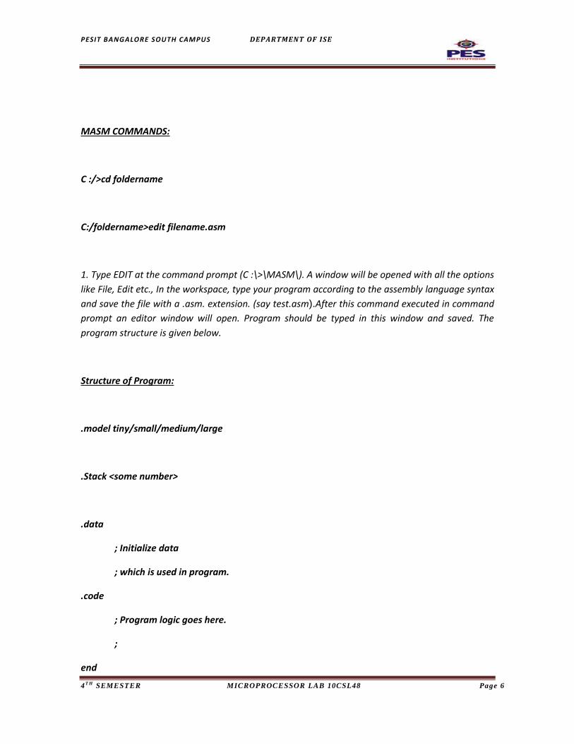
MASM COMMANDS:
C :/>cd foldername
C:/foldername>edit filename.asm
1. Type EDIT at the command prompt (C :\>\MASM\). A window will be opened with all the options
like File, Edit etc., In the workspace, type your program according to the assembly language syntax
and save the file with a .asm. extension. (say test.asm).After this command executed in command
prompt an editor window will open. Program should be typed in this window and saved. The
program structure is given below.
Structure of Program:
.model tiny/small/medium/large
.Stack <some number>
.data
; Initialize data
; which is used in program.
.code
; Program logic goes here.
;
end
PESIT BANGALORE SOUTH CAMPUS DEPARTMENT OF ISE
4T H SEMESTER MICROPROCESSOR LAB 10CSL48 Page 7
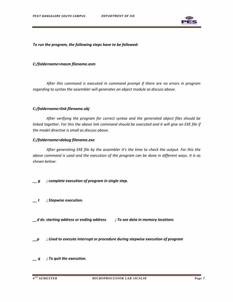
To run the program, the following steps have to be followed:
C:/foldername>masm filename.asm
After this command is executed in command prompt if there are no errors in program
regarding to syntax the assembler will generates an object module as discuss above.
C:/foldername>link filename.obj
After verifying the program for correct syntax and the generated object files should be
linked together. For this the above link command should be executed and it will give an EXE file if
the model directive is small as discuss above.
C:/foldername>debug filename.exe
After generating EXE file by the assembler it’s the time to check the output. For this the
above command is used and the execution of the program can be done in different ways. It is as
shown below:
__ g ; complete execution of program in single step.
__ t ; Stepwise execution.
__d ds: starting address or ending address ; To see data in memory locations
__p ; Used to execute interrupt or procedure during stepwise execution of program
__ q ; To quit the execution.

PESIT BANGALORE SOUTH CAMPUS DEPARTMENT OF ISE
4T H SEMESTER MICROPROCESSOR LAB 10CSL48 Page 8
Syntax of an instruction:
{label:} mnemonic {operand { , operand} } {; comment}
SIMPLIFIED SEGMENT DIRECTIVES
MASM version 5.0 and above, and TASM provide a simplified set of directives for declaring
segments called simplified segment directives. To use these directives, you must initialize a
memory model, using the .MODEL directive, before declaring any segment. The format of the
.MODEL directive is:
.MODEL memory-model
The memory-model may be TINY, SMALL, MEDIUM, COMPACT, LARGE, HUGE or
FLAT :
memory-
model
description
TINY One segment. Thus code and data together may not be greater than 64K
SMALL One code-segment. One data-segment. Thus neither code nor data may be
greater than 64K
MEDIUM More than one code-segment. One data-segment. Thus code may be greater than
64K
COMPACT One code-segment. More than one data-segment. Thus data may be greater than
64K
LARGE More than one code-segment. More than one data-segment. No array larger than
64K. Thus both code and data may be greater than 64K
HUGE More than one code-segment. More than one data-segment. Arrays may be
larger than 64K. Thus both code and data may be greater than 64K
FLAT One segment up to 4GB. All data and code (including system resources) are in a
single 32-bit segment.

PESIT BANGALORE SOUTH CAMPUS DEPARTMENT OF ISE
4T H SEMESTER MICROPROCESSOR LAB 10CSL48 Page 9
Initialization of DS
Note: The instructions which initialize the DS register for an exe-format program with
simplified segment directives are:
MOV AX , @DATA
MOV DS , AX
At load time, @DATA is replaced with the 16-bit base address of the data segment.
Comments:
A semicolon starts a comment. A comment may follow a statement or it may be on a separate
line. Multiple-line comments can be written by using the COMMENT directive.
Numbers:
A binary number is suffixed by b or B.
e.g., 11010111B
A decimal number is suffixed by an optional d or D.
e.g., 42d -22D 3578
A hexadecimal number must begin with a decimal digit and it is suffixed by h or H
e.g., 20H 0bF2Ah
Characters:
A character is enclosed in a pair of single quotes or in a pair of double quotes.
e.g., ‘x’ “B”
Strings:
A string is enclosed in a pair of single quotes or in a pair of double quotes.
e.g., ‘ENTER YOUR NAME: ’
“THE MAXIMUM VALUE IS ”

PESIT BANGALORE SOUTH CAMPUS DEPARTMENT OF ISE
4T H SEMESTER MICROPROCESSOR LAB 10CSL48 Page 10
Data definition
Each variable has a data type and is assigned a memory address by the program. The data-
defining directives are:
Directive Description of Initializers
BYTE, DB (byte) Allocates unsigned numbers from 0 to 255.
SBYTE (signed byte) Allocates signed numbers from –128 to +127.
WORD, DW (word = 2 bytes) Allocates unsigned numbers from0 to 65,535 (64K).
SWORD (signed word) Allocates signed numbers from–32,768 to +32,767.
DWORD, DD
(doubleword = 4 bytes), Allocates unsigned numbers from 0 to 4,294,967,295 (4
megabytes).
SDWORD (signed doubleword) Allocates signed numbers from –2,147,483,648 to +2,147,483,647.
A ? in place of an initializer indicates you do not require the assembler to initialize the
variable. The assembler allocates the space but does not write in it. Use ? for buffer areas or
variables your program will initialize at run time.
The DUP operator can be used to generate multiple bytes or words with known as well as un-
initialized values.
The EQU (equate) directive assigns a name to a constant expression
Syntax is:
name EQU constant_expression
Note: (i) No memory is allocated for EQU names
(ii) A name defined by EQU may not be redefined later in a program.
The LABEL directive, whose syntax is:
name LABEL type

PESIT BANGALORE SOUTH CAMPUS DEPARTMENT OF ISE
4T H SEMESTER MICROPROCESSOR LAB 10CSL48 Page 11
1. a) Search a key element in a list of ‘n’ 16-bit numbers using the Binary search
algorithm.
ALGORITHM:
Step1: Initialize low=1,high=n;
Step2: while(low<=high)
{
/*Compare low > high if true the element is not found, exit*/
Find mid
else
mid=(low+high)/2;
Step3: if(key==a[mid])
found & exit;
else if(key>a[mid])
low=mid+1;
else
high=mid-1;
}
Step4: Not found.
Step5: Stop.
Algorithm:
Step 1 : Declare the array elements in the sorted order
Step 2 : Declare the search element
Step 4 : Assign low as 0 and high as n-1
Step 5 : Find mid index = (low +high)/2
Step 6 : Compare mid element with search element
Step 7 : If search element <mid element assign high as mid-1
Step 8 : If search element >mid element, assign low as mid+1
Step 9 : If search element = mid element , the search is successful so display the
location of the search element and go to step -12
Step 10 : Repeat step 5 to 9 until the search is successful
Step 11 : If search element is not available, display “element not available” Step 12 : Terminate the program

PESIT BANGALORE SOUTH CAMPUS DEPARTMENT OF ISE
4T H SEMESTER MICROPROCESSOR LAB 10CSL48 Page 12
PROGRAM
.MODEL SMALL ; memory model
.DATA ; data segment area. Define all variables and messages
ARRAY DW 1111H,2222H,3333H,4444H,5555H ; declaring array of elements in asc order
LEN DW ($-ARRAY) ; finding length of array
KEY DW 3333H ; search element
MSG1 DB 10, 13,'ELEMENT FOUND AT POSITION $' ; message if key found
MSG2 DB 10, 13, „ELEMENT NOT FOUND$' ; message if key not found
RES DB ? 10,13,‟$‟
.CODE ; code segment starts
MOV AX, @DATA ; initializing data segment
MOV DS, AX
MOV BX, 01H ; set lower bound
MOV DX, LEN ; set upper bound
MOV CX, KEY ; move the key element to CX register
AGAIN: CMP BX, DX ; compare first and last element indexes
JA FAIL ; if lower bound>upper bound jump to FAIL
MOV AX, BX ; to calculate MID of array
ADD AX, DX ; find LOW+HIGH
SHR AX, 1 ; divide the value in AX by 2
MOV SI, AX
DEC SI
ADD SI, SI ; 2(AX-1) gives actual index of mid
CMP CX, ARRAY [SI] ; compare CX and the array element at MID
JAE BIGGER ; if equal jump to BIGGER

PESIT BANGALORE SOUTH CAMPUS DEPARTMENT OF ISE
4T H SEMESTER MICROPROCESSOR LAB 10CSL48 Page 13
DEC AX ; search elements below MID
MOV DX, AX ; HIGH=MID-1
JMP AGAIN ; jump to AGAIN
BIGGER: JE SUCCESS ; jump if equal to SUCCESS
INC AX ; search elements above MID
MOV BX, AX ; LOW=MID+1
JMP AGAIN ; unconditional jump to repeat the above
FAIL: LEA DX, MSG2 ;if not found display mesg2
MOV AH, 09H ;service no. to display message
INT 21H
JMP EXIT ; interrupt to terminate
SUCCESS: ADD AL,'0' ;get ASCII value of key position
MOV RES, AL
LEA DX, MSG1 ;if key element found display MESG1
MOV AH, 09H ;service no. to display message
INT 21H
MOV DL, RES ;display key position
MOV AH, 02H
INT 21H
EXIT: MOV AH, 4CH ;interrupt to return to DOS
INT 21H
END
*********************************

PESIT BANGALORE SOUTH CAMPUS DEPARTMENT OF ISE
4T H SEMESTER MICROPROCESSOR LAB 10CSL48 Page 14
OUTPUT:
KEY=3333H ELEMENT FOUND
KEY=3331H ELEMENT NOT FOUND
RESULT: This program performs a search for a key element in an array. If the search
element is found a message „found‟ is displayed. If the search element (key in program) is
not present in the given array a message „not found‟ is displayed.

PESIT BANGALORE SOUTH CAMPUS DEPARTMENT OF ISE
4T H SEMESTER MICROPROCESSOR LAB 10CSL48 Page 15
2. Sort a given set of ‘n’ numbers in ascending order using the Bubble Sort algorithm.
Algorithm:
Step 1: Initialize array elements in data segment.
Step 2: Initialize the number of elements in a array(N-array)
Number of elements in array (N)
=current address of memory pointer ($)– array of Array N(array name)
Step 3: Where List is array of ‘n’ elements
Bubble(int(list[],know)
{
int i,j;
for(i=1;i<=n;i++)
for(j=1;j<=n-i;j++)
if(list[j]>=list[j+1])
swap(list[j],list[j+1])
}
Step 4: Stop
ALGORITHM
Step 1 : Declare the array with the numbers that need to be sorted.
Step 2 : Initialize iteration count (n-1)
Step 3 : Initialize comparison counter
Step 4 : Compare num1 and num2
Step 5 : Num1<=num2 do not exchange
Step 6 : Num1>=num2 then exchange the positions of both numbers
Step 7 : Decrement iteration counter, comparison counter
Step 8 : Terminate the program

PESIT BANGALORE SOUTH CAMPUS DEPARTMENT OF ISE
4T H SEMESTER MICROPROCESSOR LAB 10CSL48 Page 16
PROGRAM FOR ARRAY OF N 8-BIT NUMBERS
.MODEL SMALL
.STACK 64 ;stack segment
.DATA ;data segment
ARR DB 10H, 08H, 04H, 09H, 06H ;byte definition of array
LEN DB ($-ARR) ;length of the array
.CODE
MOV AX,@DATA ; initialise data segment
MOV DS, AX
MOV BL, LEN ;move the length into BL
DEC BL ;decrement BL by 01
OUTLOOP: MOV CL, BL ;move BL value into CL
MOV SI, 00H ;initialize SI to 00H
INLOOP: MOV AL, ARR[SI] ;move A[SI] into AL register
CMP AL, ARR[SI+1] ;compare values in AL and ARR[SI]
JB NEXT ;if AL<A[SI+1],jump to NEXT
XCHG AL,ARR[SI+1] ;swap values of AL and A[SI]
MOV ARR[SI],AL
NEXT: INC SI ;increment SI value by 01
LOOP INLOOP
DEC BL ;decrement BL value by 01
JNZ OUTLOOP ;jump to outloop till ZF=1
MOV AH,4CH ;end program
INT 21H
END

PESIT BANGALORE SOUTH CAMPUS DEPARTMENT OF ISE
4T H SEMESTER MICROPROCESSOR LAB 10CSL48 Page 17
OUTPUT:
-G
-D DS:0000
13F7:0000 0A 00 46 E2 EB FE CB 75-E2 CC 04 06 08 09 10 00

PESIT BANGALORE SOUTH CAMPUS DEPARTMENT OF ISE
4T H SEMESTER MICROPROCESSOR LAB 10CSL48 Page 18
PROGRAM FOR ARRAY OF N 16-BIT NUMBERS
.MODEL SMALL
.DATA
ARR DW 0020H,0070H,0040H,0010H,0050H ;word definition of array
CNT EQU 5
.CODE
MOV AX, @DATA ;initialise data segment
MOV DS, AX
MOV DX, CNT-1 ; no of iterations in DX reg
AGAIN0: MOV CX, DX ; no of comparisons
LEA SI, ARR ; SI = index of the array
AGAIN1: MOV AX, [SI] ; value of ARR [SI] moved to AX register
CMP AX, [SI+2] ; comparing elements ARR[SI] and ARR[SI+2]
JL LOOP1 ; exchange not required if ARR[SI] <ARR[SI+2]
XCHG [SI+2], AX ; exchange elements if bigger
XCHG [SI], AX
LOOP1: ADD SI, 02 ;repeat with every two numbers
LOOP AGAIN1 ;decrement number of comparisons
DEC DX ;decrement number of iterations each time
JNZ AGAIN0
MOV AH, 4CH ;terminate program
INT 21H
END
**************************
OUTPUT:
ASCENDING ORDER: 0010H, 0020H, 0040H, 0050H, 0070H
RESULT: This program performs an ascending order sort on given array. It will store the result in
data segment. The data segment memory location is observed for given array.

PESIT BANGALORE SOUTH CAMPUS DEPARTMENT OF ISE
4T H SEMESTER MICROPROCESSOR LAB 10CSL48 Page 19
3. Reverse a given string and check whether it is a palindrome or not.
Algorithm:
Step 1: Initialise a string (STR)
Step 2: SI points to the initial memory location and store the string in [SI].
Step 3: If [SI] is entered string then go to Step 4 to display the reversed string.
Step 4: Decrease SI by 1 location and move the content of SI to DI register. DI is assumed to point
at the reverse string.
Step 5: Compare the characters which is stored in SI and DI. If equal, display (“Palindrome”) using
‘09H’ service.
Else display (“Not a Palindrome”) using 09H service.
Step 6: Stop.
Algorithm:
Step 1 : Create display macro to display the message
Step 2: Declare the string
Step 3: Declare the message to display
Step 4: Find the reverse of string and store in string1
Step 5: Is string=string1, display it is a palindrome
Step 6: Else if display not a palindrome
Step 7: Terminate the program

PESIT BANGALORE SOUTH CAMPUS DEPARTMENT OF ISE
4T H SEMESTER MICROPROCESSOR LAB 10CSL48 Page 20
PROGRAM
DISP MACRO MSG
LEA DX, MSG
MOV AH, 09H
INT 21H
ENDM
.MODEL SMALL
.DATA
STR DB "MALAYALAM$" ; array to store original string
LEN EQU ($-STR)
MSG1 DB 10, 13,"PALINDROME$"
MSG2 DB 10, 13,"NOT A PALINDROME$"
RSTR DB 40 DUP (0) ; array to store reverse string
.CODE
MOV AX, @DATA ; Initialisation of Data Segment
MOV DS, AX
MOV ES, AX ; Initialisation of Extra Segment
MOV CX,LEN
DEC CX
LEA SI, STR ;EA of STR is loaded to SI register
ADD SI,CX
DEC SI
LEA DI, RSTR ; EA of RSTR is loaded to DI register
AGAIN: MOV AL, [SI] ; Character in location pointed by SI is copied to AL
MOV [DI], AL ; Character in AL is copied to location pointed by DI
DEC SI ; decrements SI to point to next character of reversed string

PESIT BANGALORE SOUTH CAMPUS DEPARTMENT OF ISE
4T H SEMESTER MICROPROCESSOR LAB 10CSL48 Page 21
INC DI ; increments DI to point to next character of entered string
DEC CX
CMP CX,0000H
JNZ AGAIN ;continue process till CL Register =Zero
MOV AL,"$"
MOV [DI],AL
LEA SI, STR
LEA DI, RSTR
MOV CX,LEN
REPE CMPSB ; compare original and reversed strings
JE PALIN ; if equal jump to PALIN
DISP MSG2 ; Display Message NOT PALINDROME
JMP EXIT
PALIN: DISP MSG1 ; Display Message PALINDROME
EXIT:MOV AH, 4CH
INT 21H
END
OUTPUT:
ABCDDCBA IS A PALINDROME
ABCDDC NOT A PALINDROME
*******************************************************************************
******
RESULT: This program reverses the string provided in data segment by keeping the original string
as it is and compares both the strings. It will check each and every character. If all the characters
are same then the given string is said to be as palindrome and it will display a message
“palindrome” on screen otherwise the given string is not palindrome and it will display a message
“not palindrome” on screen.

PESIT BANGALORE SOUTH CAMPUS DEPARTMENT OF ISE
4T H SEMESTER MICROPROCESSOR LAB 10CSL48 Page 22
4. Compute nCr using recursive procedure. Assume that ‘n’ and ‘r’ are non-
negative integers.
Algorithm 1:
Step 1: if r=0 or n=r then nCr=1
Step 2: if r=1 or r=n-1 then nCr=n
Step 3: Recursive definition of nCr is nCr= (n-1)Cr + (n-1)C(r-1)
Algorithm 2:
nCr(r,n)
{
If(r==0 || n==r)
Return(1);
Else
If(r==1 || r==n-1)
Return(n);
Return(nCr (r,n-1)+ (n-1)Cr(r-1,n-1));
}

PESIT BANGALORE SOUTH CAMPUS DEPARTMENT OF ISE
4T H SEMESTER MICROPROCESSOR LAB 10CSL48 Page 23
PROGRAM
.MODEL SMALL
.DATA
N DW 6H
R DW 3H
NCR DW 01 DUP (0) ; to store the result
MSG1 DB 10, 13, “Error $"
.CODE
MOV AX, @DATA ; initialize data segment
MOV DS, AX
MOV AX, N ; AX has value of N
MOV BX, R ; BX has value of R
CALL NCRPROC
MOV AH, 4CH
INT 21H
NCRPROC PROC
CMP AX, 0 ; if n=0, error condition
JZ Error
CMP BX, AX ; if n=r, ncr value is 1
JG Error
JE RES1
CMP BX, 0 ; if r=0, ncr value is 1
JE RES1
DEC AX
CMP BX, 1 ; if r=1, ncr value is n
JE RESN
CMP BX, AX ; if r=n-1, ncr value is n
JE RESN

PESIT BANGALORE SOUTH CAMPUS DEPARTMENT OF ISE
4T H SEMESTER MICROPROCESSOR LAB 10CSL48 Page 24
PUSH AX
PUSH BX
CALL NCRPROC
POP BX
POP AX
DEC BX
PUSH AX
PUSH BX
CALL NCRPROC
POP BX
POP AX
RET
Error: LEA DX, MSG1 ; display message
MOV AH, 09H
INT 21H
RES1: INC NCR
RET
RESN: INC NCR ;initial ncr value=0 is incremented r=2 times(0+1+1)
ADD NCR, AX ;(1+5=6,6+4=10,10+3=13,13+2=15),i.e,[1+(n-1)+(n-2)+(n-3)+(n-4)]
RET ;addition is carried out (n-1) times
NCRPROC ENDP
END
*******************************************************************************
******

PESIT BANGALORE SOUTH CAMPUS DEPARTMENT OF ISE
4T H SEMESTER MICROPROCESSOR LAB 10CSL48 Page 25
OUTPUT:
CASE1: N=0 R=2
Error
CASE 2: N=2 R=3
Error!
CASE3: N=3, R=3
NCR=1
CASE4: N=3, R=0
NCR=1
CASE5: N=3, R=1
NCR=3
CASE 6: N=3, R=2
NCR=3
CASE7: N=6, R=2
NCR=0FH
RESULT: This program performs nCr using recursive procedure. Output is stored in data
segment. The output is observed in data segment.
Note: From Pascal‟s triangular relation, nCr =
n-1Cr +
n-1Cr-1
In this formulation, one thing is to be noted that n and r keep decreasing, and sometimes is is
possible that n becomes smaller than r. So considering these cases the base conditions for the
recursive formula are,
nCn = 1,
nC1 = n,
nC0 = 1 and
nCr =
n-1Cr +
n-1Cr-1

PESIT BANGALORE SOUTH CAMPUS DEPARTMENT OF ISE
4T H SEMESTER MICROPROCESSOR LAB 10CSL48 Page 26
5. Read the current time and date from the system and display it in the standard format
on the screen.
Algorithm
Step 1: Read the system time using ‘2CH’ service number.
Step 2: To display the hour, minute, seconds, convert from hexadecimal to BCD using ‘AAM’
instruction.
Step 3: Display using ‘02H’ service number.
Step 4: Stop.
Step 5: Read the system time using ‘2AH’ service number.
Step 6: To display the date, month, year, convert from hexadecimal to BCD using ‘AAM’ instruction.
Step 7: Display using ‘02H’ service number.
Step 8: Stop.

PESIT BANGALORE SOUTH CAMPUS DEPARTMENT OF ISE
4T H SEMESTER MICROPROCESSOR LAB 10CSL48 Page 27
PROGRAM
CLRSCR MACRO ; macro definition to clear screen
MOV AL, 02H
MOV AH, 00H
INT 10H
ENDM
.MODEL SMALL
.DATA
msg1 DB 10, 13,'The system time is: $'
msg2 DB 10, 13,'The system date is: $'
.CODE
MOV AX,@DATA
MOV DS,AX
CLRSCR
LEA DX,msg1
MOV AH,09H
INT 21H
MOV AH,2CH ; DOS function to read system time
INT 21H
MOV AL, CH ; Hours in CH register
AAM ; unpack the digits
MOV BX, AX
CALL DISP ; use a procedure to convert to ASCII and display on screen
MOV DL,':' ; the format is hh: mm: ss
MOV AH, 02H
INT 21H
MOV AL, CL ; minutes in CL register
AAM

PESIT BANGALORE SOUTH CAMPUS DEPARTMENT OF ISE
4T H SEMESTER MICROPROCESSOR LAB 10CSL48 Page 28
MOV BX,AX
CALL DISP
MOV DL,':'
MOV AH, 02H
INT 21H
MOV AL, DH ; seconds in DH register
AAM
MOV BX,AX
CALL DISP
LEA DX,msg2
MOV AH,09H
INT 21H
DAY: MOV AH, 2AH ; DOS Function to get System Date
INT 21H
MOV AL, DL ; Day is in DL
AAM
MOV BX, AX
CALL DISP
MOV DL,'/'
MOV AH, 02H ; To Print / in DOS
INT 21H
MONTH:MOV AH, 2AH ; To get System Date
INT 21H
MOV AL, DH ; Month is in DH
AAM
MOV BX, AX
CALL DISP

PESIT BANGALORE SOUTH CAMPUS DEPARTMENT OF ISE
4T H SEMESTER MICROPROCESSOR LAB 10CSL48 Page 29
MOV DL,'/' ; To Print / in DOS
MOV AH, 02H
INT 21H
YEAR: MOV AH, 2AH ; To get System Date
INT 21H
ADD CX, 0F830H ; To negate the effects of 16bit value,
MOV AX, CX ; since AAM is applicable only for AL (YYYY -> YY)
AAM
MOV BX, AX
CALL DISP
MOV AH, 4CH
INT 21H
DISP PROC NEAR ; convert to ASCII and display
MOV DL, BH
ADD DL, 30h
MOV AH, 02h
INT 21h
MOV DL, BL
ADD DL, 30h
MOV AH, 02h
INT 21h
RET
DISP ENDP
END
*********************************************************************************
OUTPUT: The system time is: 12:02:06
The system date is: 03/12/16
RESULT: This program displays the present system time. The program displays the hours and
minutes and seconds in the format HH:MM: SS.
This program displays the present system date. The program displays the days, months and year in
the format DD/MM/YY.

PESIT BANGALORE SOUTH CAMPUS DEPARTMENT OF ISE
4T H SEMESTER MICROPROCESSOR LAB 10CSL48 Page 30
8. Implement a BCD Up-Down Counter on the Logic Controller Interface.
D7 D6 D
5
D4 D3 D2 D1 D0
82H
1 0 0 0 0 0 1 0
I/O
Functio
n
Port A in
Mode 0
Port
A as
O/P
Port CU
As
O/P
Port B in
Mode 0
Port B
As I/P
Port
CL
As
O/P

PESIT BANGALORE SOUTH CAMPUS DEPARTMENT OF ISE
4T H SEMESTER MICROPROCESSOR LAB 10CSL48 Page 31
Algorithm:
Step 1: Connect Logic Controller to PC.
Step 2: Set the 8255 using control word, initialize the control word i.e., 82H
Step 3: Store the control word in the Control register.
Step 4: Initialize the counter to 10(count to loop for displaying up counter), and AL with 00.
Step 5: Initialize the Port A address and display the contains of AL, call some delay and add 01h to
AL and again display it. Loop repeats until counter becomes 0.
Step 6: Again initialize counter to 10, and AL with 00, each time subtract 01 from AL and display
contents of AL, until counter becomes 0.
Step 7: Initialize the counter with 09H and AL, with 01H, display the contents of AL.
Step 8: Rotate the contains of AL once loop back and again display AL, the loop repeats until
counter becomes 0.
Step 9: Stop
PESIT BANGALORE SOUTH CAMPUS DEPARTMENT OF ISE
4T H SEMESTER MICROPROCESSOR LAB 10CSL48 Page 32
PROGRAM:
.MODEL SMALL
.DATA
MSG1 DB “UP COUNTER STARTS $”
MSG2 DB “DOWN COUNTER STARTS $”
.CODE
MOV AX,@DATA ; Initialise data segment
MOV DS, AX
MOV DX, 9803H ; Control Word Register address
MOV AL, 82H ; set 8255 port B as input and port A and port C as output
OUT DX, AL
MOV CX, 0AH
LEA DX, MSG1
MOV AH, 09H
INT 21H
MOV AL, 00 ; AL holds initial count for BCD up counter
UP: MOV DX, 9800H
OUT DX, AL
INC AL ; increment count
DAA
CALL DELAY
LOOP UP
MOV CX, 0AH
LEA DX, MSG1
MOV AH, 09H
INT 21H

PESIT BANGALORE SOUTH CAMPUS DEPARTMENT OF ISE
4T H SEMESTER MICROPROCESSOR LAB 10CSL48 Page 33
DOWN: MOV DX, 9800H
OUT DX, AL
DEC AL ; decrement count
DAS
CALL DELAY
LOOP DOWN
QUIT: MOV AH, 4CH
INT 21H
DELAY PROC
PUSH BX
PUSH DX
MOV DX,0FFFFH
OUTER : MOV BX,0FFFFH
INNER : DEC BX
JNZ INNER
DEC DX
JNZ OUTER
POP DX
POP BX
RET
DELAY ENDP
END
*********************************************************************************
OUTPUT:
UPCOUNTER
0000 0001 0010 0011 0100 0101 0110 0111 1000 1001
DOWNCOUNTER
1001 1000 0111 0110 0101 0100 0011 0010 0001 0000

PESIT BANGALORE SOUTH CAMPUS DEPARTMENT OF ISE
4T H SEMESTER MICROPROCESSOR LAB 10CSL48 Page 34
RESULT: The program performs the up-down counter based on the input data given on logic
controller read through port B. If the input is zero down counter starting from 99 down to 00 is
executed and if other than zero is the input then up counter starting from 00 down to 99 is executed.
The counting will continue until a key is pressed in the key board.

PESIT BANGALORE SOUTH CAMPUS DEPARTMENT OF ISE
4T H SEMESTER MICROPROCESSOR LAB 10CSL48 Page 35
8b. Read the status of two 8-bit inputs (X & Y) from the Logic Controller Interface and
display X*Y.
D7 D6 D
5
D4 D3 D2 D1 D0
82H
1 0 0 0 0 0 1 0
I/O
Functio
n
Port A in
Mode 0
Port
A as
O/P
Port CU
As
O/P
Port B in
Mode 0
Port B
As I/P
Port
CL
As
O/P

PESIT BANGALORE SOUTH CAMPUS DEPARTMENT OF ISE
4T H SEMESTER MICROPROCESSOR LAB 10CSL48 Page 36
ALGORITHM:
Step 1: Connect Logic Controller to PC.
Step 2: Set the 8255 using control word.
Step 3: Read the first data (Port B) from logic controller and store in X.
Step 4: Read the second data (Port B) from logic controller and store in Y.
Step 5: res=X*Y
Display(higher 8 bit data of res)
Step 6: Call delay procedure or wait some time.
Step 7: Stop

PESIT BANGALORE SOUTH CAMPUS DEPARTMENT OF ISE
4T H SEMESTER MICROPROCESSOR LAB 10CSL48 Page 37
PROGRAM:
.MODEL SMALL
.DATA
MSG1 DB "ENTER VALUE OF X FROM THE INTERFACE: $"
MSG2 DB "ENTER VALUE OF Y FROM THE INTERFACE: $"
.CODE
MOV AX,@DATA
MOV DS,AX
MOV DX, 9803H ;initialize 8255 ports
MOV AL, 82H ;CW=82H Port B=Input Port,PortA=Output Port
OUT DX, AL
MOV DX , OFFSET MSG1
MOV AH , 09H
INT 21H
MOV DX, 9801H ;read first number X through port B of 8255
IN AL, DX
MOV BL, AL ; first number copied to BL reg
MOV DX ,OFFSET MSG2
MOV AH , 09H
INT 21H
MOV DX,9801H ;read second number through port B of 8255
IN AL,DX
MUL BL ; 16-bit product in AX reg
MOV DX,9800H ; send lower byte of the product to port A for display
OUT DX,AL
MOV AL,AH
OUT DX, AL ; send higher byte of the product to port A for display
MOV AH, 4CH ;terminate program
INT 21H
END

PESIT BANGALORE SOUTH CAMPUS DEPARTMENT OF ISE
4T H SEMESTER MICROPROCESSOR LAB 10CSL48 Page 38
OUTPUT:
X00000011
Y00000010
PRODUCT: 00000110
RESULT: The program performs the multiplication between two bytes and gives the result. A
message appears on the screen to enter the first number. First byte is read from the port B of
logic controller and once enter key is pressed the second number is read from port B and
enter key is to be pressed. Result will be displayed on the port A of the logic controller.

PESIT BANGALORE SOUTH CAMPUS DEPARTMENT OF ISE
4T H SEMESTER MICROPROCESSOR LAB 10CSL48 Page 39
9. Display messages FIRE and HELP alternately with flickering effects on a 7- segment
display interface for a suitable period of time. Ensure a flashing rate that makes it easy
to read both the messages (Examiner does not specify these delay values nor is it
necessary for the student to compute these values).
A seven segment display consists of seven LEDs arranged in the form of a squarish ‘8’ slightly
inclined to the right and a single LED as the dot character.
Different characters can be displayed by selectively glowing the required LED segments. Seven
segment displays are of two types, common cathode and common anode.
In common cathode type , the cathode of all LEDs are tied together to a single terminal which is
usually labelled as „com„ and the anode of all LEDs are left alone as individual pins labelled as
a, b, c, d, e, f, g & h (or dot) .
In common anode type, the anodes of all LEDs are tied together as a single terminal and cathodes
are left alone as individual pins. The pin out scheme and picture of a typical 7 segment LED
display is shown in the image below.
D7 D6 D5 D4 D3 D2 D1 D0
1 0 0 0 0 0 0 0
I/O
function
Port A in Mode 0 Port A as O/P Port CU
As O/P
Port B in
Mode 0
Port B
As O/P
Port
CL
As
O/P
80H
dp g f e D b c a
F 1 0 0 0 1 1 1 0 8EH
I 1 1 1 1 1 0 0 1 0F9H
R 1 0 0 0 1 0 0 0 88H
E 1 0 0 0 0 1 1 0 86H
H 1 0 0 0 1 0 0 1 89H
E 1 0 0 0 0 1 1 0 86H
L 1 1 0 0 0 1 1 1 0C7H
P 1 0 0 0 1 1 0 0 8CH

PESIT BANGALORE SOUTH CAMPUS DEPARTMENT OF ISE
4T H SEMESTER MICROPROCESSOR LAB 10CSL48 Page 40
Algorithm:
Step 1: Connect Multiplex seven segment interface to PC.
Step 2: Set the 8255 using control word, initialize the control word i.e., 80H
Step 3: Store the control word in the Control register.
Step 4: Point the SI to FIRE and call display procedure.
Step 5: Display Procedure:
i) Initialize the counter to 4 to display 4 digit seven segment number.
ii) Move the contents of pointer to AL (which points to FIRE and HELP).
iii) Initialize Port A address and load the string byte to display on the seven segment display and the
pointer automatically increments to point to the next character (in the FIRE and HELP).
iv) Introduce some delay between each display and enable next digit D2 and so on until all the digits
from D1 to D4 is displayed.
Step 6: Point the SI to HELP and call display procedure
Step 7: Repeat from Step5 to Step8.
Step 8: To stop the display use service number 06H with DL content as 0FFH.
Step 9: Stop

PESIT BANGALORE SOUTH CAMPUS DEPARTMENT OF ISE
4T H SEMESTER MICROPROCESSOR LAB 10CSL48 Page 41
PROGRAM
.MODEL SMALL
.DATA
FIRE DB 86H, 88H, 0F9H, 8EH ; initialize segment display value of FIRE
HELP DB 8CH, 0C7H, 86H, 89H ; initialize segment display value of HELP
.CODE
START : MOV AX,@DATA ;initialize data segment
MOV DS,AX
MOV DX,9803H ;initialize CWR
MOV AL,80H ; All ports are output ports
OUT DX,AL
MOV BH,0AH ;initialize number of times FIRE and HELP are displayed
AGAIN: MOV SI, OFFSET FIRE
CALL DISPLAY
CALL DELAY
MOV SI, OFFSET HELP
CALL DISPLAY
CALL DELAY
DEC BH ;decrement display count
CMP BH,00H
JE TERMINATE ;repeat till display count=0
JNZ AGAIN
DISPLAY PROC
MOV CX,04H ;initialize CX=4,as 4 displays are used
LOOP2 : MOV BL,08H ;initialize eight letters to BL register
MOV AL,[SI] ;copy first letter to AL

PESIT BANGALORE SOUTH CAMPUS DEPARTMENT OF ISE
4T H SEMESTER MICROPROCESSOR LAB 10CSL48 Page 42
NEXT : ROL AL,01H ;rotate contents of AL to the left
MOV DX,9801H ;initialize DX with port B address
OUT DX,AL ;send contents of AL to output port
PUSH AX
MOV AL,0FFH ; initialize AL=FFH,i/p =high
INC DX ; ;initialize DX with port C address
OUT DX,AL ;send high input to output port
MOV AL,00H ;initialize AL=00H,i/p =low
OUT DX,AL ;send low input to output port
DEC BL ; repeat 08 times
POP AX
JZ NEXT1
JMP NEXT
NEXT1 : INC SI ;get next letter
LOOP LOOP2 ;continue display till CX=0
RET
DISPLAY ENDP
DELAY PROC
PUSH AX
PUSH CX
MOV CX,0FFFH
LOOP1 : MOV AX,0FFFFH
LOOP3 : DEC AX
JNZ LOOP3
LOOP LOOP1
POP CX
POP AX

PESIT BANGALORE SOUTH CAMPUS DEPARTMENT OF ISE
4T H SEMESTER MICROPROCESSOR LAB 10CSL48 Page 43
RET
DELAY ENDP
TERMINATE: MOV AH, 4CH
INT 21H
END START
*************************************************************************
Output: F I R E
H E L P
RESULT: This program displays “FIRE” and “HELP” on seven segment display interface
recursively one after the other with some delay till a key is pressed on key board. The data
which has to be displayed is provided in the program itself.

PESIT BANGALORE SOUTH CAMPUS DEPARTMENT OF ISE
4T H SEMESTER MICROPROCESSOR LAB 10CSL48 Page 44
10. Drive a Stepper Motor interface to rotate the motor in specified direction
(clockwise or counter-clockwise) by N steps (Direction and N are specified by the
examiner). Introduce suitable delay between successive steps. (Any arbitrary value
for the delay may be assumed by the student).
A stepper motor is a widely used device that translates electrical pulses into mechanical movement. In
applications such as disk drives, dot matrix printers, and robotics, the stepper motor is used for
Position control. Every stepper motor has a permanent magnet rotor (also called the shaft.) surrounded
by a stator. The most common stepper motors have four common stator windings that are pairs with a
center-taped common. This type of stepper motor is commonly referred to as a four-phase stepper
motor.
A Stepper motor is stepped from one position to the next by changing the currents through the fields
in the motor. Common step sizes for stepper motors range from 0.9 degrees to 30 degrees.
Stepper motor is interfaced to 8086 with the help of 8255 IC (Programmable Peripheral Interface).
82C55A is used to provide the drive signals that are used to rotate the armature of the motor in either
the right-hand or left-hand direction. Stepper motor is IO device so CW should be (80) H.

PESIT BANGALORE SOUTH CAMPUS DEPARTMENT OF ISE
4T H SEMESTER MICROPROCESSOR LAB 10CSL48 Page 45
The power circuit for one winding of the stepper motor is as shown in figure above. It is connected to
the port A (PA0) of 82C55A. Similar circuits are connected to the remaining lower bits of port A
(PA1, PA2, PA3). One winding is energized at a time. The coils are turned ON/OFF one at a time
successively.
The stepper motor showing full-step operation is shown below.
(A) 45-degrees. (B) 135-degrees
(C) 225-degrees (D) 315-degrees.

PESIT BANGALORE SOUTH CAMPUS DEPARTMENT OF ISE
4T H SEMESTER MICROPROCESSOR LAB 10CSL48 Page 46
There are three commonly used excitation modes for step motors; these are full step, half step and
microstepping. In full step operation, the motor moves through its basic step angle, i.e., a 1.8° step motor takes
200 steps per motor revolution.
A typical stepper motor may have parameters like torque 3 kg-em, operating voltage 12V, current
rating 1.2A and a step angle 1.8 degree, i.e. 200 steps/revolution (number of rotor teeth).
Number of rotor teeth=200 steps/revolution
θR = 360degree/Number of rotor teeth
=360 degree/200=1.8 degree
Count N= Number of rotor teeth * θ =200*1.8 degree = 1 rotation
360 360
D7 D6 D5 D4 D3 D2 D1 D0
1 0 0 0 0 0 0 0
I/O
function
Port A in Mode
0
Port A as
O/P
Port
CU
As
O/P
Port B
in
Mode 0
Port B
As
O/P
Port
CL
As
O/P
80H

PESIT BANGALORE SOUTH CAMPUS DEPARTMENT OF ISE
4T H SEMESTER MICROPROCESSOR LAB 10CSL48 Page 47
Algorithm:
Step 1: Initialize the control word 80H and store it in the control register.
Step 2: Initialize the number of steps (N) the stepper motor has to rotate.
Step 3: Coils are selected by storing 88H in AL register that is current is passed through coil.
Step 4: Send the data through Port C, hence initialize the Port C address.
Step 5: For clockwise rotation rotate the contents of AL register to right by 1 using ROR instruction
and decrease the steps. For anticlockwise rotation rotate the contents of AL register to left by 1
using ROL instruction and decrease the steps.
Step 6: Introduce delay counter after each steps.
Step 7: Repeat the steps 5 & 6 until n>0
Step 8: Stop.

PESIT BANGALORE SOUTH CAMPUS DEPARTMENT OF ISE
4T H SEMESTER MICROPROCESSOR LAB 10CSL48 Page 48
PROGRAM:
.MODEL SMALL
.DATA
N DW 200 ; no of rotations. N=200 is one rotation
.CODE
MOV AX,@DATA
MOV DS, AX
MOV DX, 09803H
MOV AL, 80H
OUT DX,AL
MOV DX, 09800H
MOV AL,88H ; load pattern to energize the windings of motor into AL
MOV CX,N
AGAIN : OUT DX,AL ; energize winding of the motor
CALL DELAY
ROR AL,01 ; clockwise rotation
LOOP AGAIN
MOV CX,N
AGAIN1: OUT DX, AL
CALL DELAY
ROL AL,01
LOOP AGAIN1
MOV AH,4CH
INT 21H

PESIT BANGALORE SOUTH CAMPUS DEPARTMENT OF ISE
4T H SEMESTER MICROPROCESSOR LAB 10CSL48 Page 49
DELAY PROC ; delay procedure
PUSH BX
PUSH CX
MOV CX, 0FFFH
REPEAT: MOV BX, 0FFFFH
HERE1: DEC BX
JNZ HERE1
LOOP REPEAT
POP CX
POP BX
RET
DELAY ENDP
END
*********************************************************************************
***
RESULT: This program drives a stepper motor interface to rotate by N steps in clockwise and anti-
clockwise direction. After each rotation a delay is introduced to observe the rotation. After the
rotations are completed the execution is stopped.

PESIT BANGALORE SOUTH CAMPUS DEPARTMENT OF ISE
4T H SEMESTER MICROPROCESSOR LAB 10CSL48 Page 50
11a. Generate the Sine Wave using DAC interface (The output of the DAC
is to be displayed on the CRO).
The pin details of DAC 0800 is given below and schematic diagram of the dual DAC
interface is given below.
The port A and port B of 82C55A peripheral are used as output ports. The digital inputs to
the DACs are provided through these ports. The analog outputs of the DACs are connected to
the inverting inputs of OP-amps 741 which acts as current to voltage converters. The outputs
from the OP-amps are connected to points marked X out and Y out at which the waveforms
are observed on a CRO. The power supplies of +12 and -12 are regulated for this interface.

PESIT BANGALORE SOUTH CAMPUS DEPARTMENT OF ISE
4T H SEMESTER MICROPROCESSOR LAB 10CSL48 Page 51
D7 D6 D5 D4 D3 D2 D1 D0
1 0 0 0 0 0 0 0
I/O
function
Port A in Mode 0 Port A as O/P Port CU
As O/P
Port B in
Mode 0
Port B
As O/P
Port CL
As O/P
80H
Algorithm:
Calculate table values using the formula table[i]=127+127SinӨ (Equation to generate sine
wave) where Ө ranges from 0 to 180 in steps of 6 degree.
Step 1: Initialize the control word 80H and store it in the control register.
Step 2: Initialize the Port A address and initialize the counter to 31(total number of elements
in table).
Step 3: For (i=0 to31)
Out-port(Port A, Table[i]) ; /*will get +ve half cycle of sine wave
For (i=0 to 31)
Out-port(Port A, -table[i]) ;/*will get –ve half cycle of sine wave
Step 4: Stop.

PESIT BANGALORE SOUTH CAMPUS DEPARTMENT OF ISE
4T H SEMESTER MICROPROCESSOR LAB 10CSL48 Page 52
Angle vs. Voltage Magnitude for Sine Wave
Angle θ
(degrees)
Sin θ θ Values
Sent to
DAC
(decimal)
=
127+127
Sin θ
θ Values
Sent to
DAC
Hexadecim
al
Angle θ
(degrees
)
Sin θ θ Values
Sent to
DAC
(decimal)
=
127+127
Sin θ
θ Values
Sent to DAC
(Hexadecim
al)
0 0 127 7F 186 -0.104 114 72H
6 0.104 140 8CH 192 -0.207 101 65H
12 0.207 153 99H 198 -0.309 88 58H
18 0.309 166 0A6H 204 -0.406 75 4CH
24 0.406 178 0B2H 210 -0.5 64 3FH
30 0.5 191 0BFH 216 -0.587 52 34H
36 0.587 201 0CAH 222 -0.66 42 2AH
42 0.66 212 0D4H 228 -0.743 33 21H
48 0.743 221 0DDH 234 -0.809 24 18H
54 0.809 230 0E6H 240 -0.866 17 11H
60 0.866 237 0EDH 246 -0.91 11 0BH
66 0.91 243 0F3H 252 -0.95 6 06H
72 0.95 248 0F8H 258 -0.978 3 03H
78 0.978 251 0FDH 264 -0.994 1 01H
84 0.994 253 0FCH 270 -1 0 00H
90 1 254 0FBH 276 -0.994 1 01H
96 0.994 253 0FCH 282 -0.978 3 03H
102 0.978 251 0FDH 288 -0.95 6 06H
108 0.95 248 0F8H 294 -0.91 11 0BH
114 0.91 243 0F3H 300 -0.866 17 11H
120 0.866 237 0EDH 306 -0.809 24 18H
126 0.809 230 0E6H 312 -0.743 33 21H
132 0.743 221 0DDH 318 -0.66 42 2AH
138 0.66 212 0D4H 324 -0.587 52 34H
144 0.587 201 0CAH 330 -0.5 64 3FH
150 0.5 191 0BFH 336 -0.406 75 4CH
156 0.406 178 0B2H 342 -0.309 88 58H
162 0.309 166 0A6H 348 -0.207 101 65H
168 0.207 153 99H 354 -0.104 114 72H
174 0.104 140 8CH 360 0 127 7FH
180 0 127 7FH
PESIT BANGALORE SOUTH CAMPUS DEPARTMENT OF ISE
4T H SEMESTER MICROPROCESSOR LAB 10CSL48 Page 53
PROGRAM
.MODEL SMALL
.DATA
ARR DB 7FH,8CH,99H,0A6H,0B2H,0BFH,0CAH,0D4H,0DDH,0E6H,0EDH,0F3H,0F8H,0FDH,0FCH,
DB 0FBH,0F8H,0F3H,0EDH,0E6H,0DDH,0D4H,0CAH,0BFH,0B2H,0A6H,99H,08CH,7FH,72H,
DB 65H,58H,4CH,3FH,34H,2AH,21H,18H,11H,0BH,06H,03H,01H,00H,01H,
DB 03H, 06H,0BH,11H,18H,21H,2AH,34H,3FH,4CH,58H,65H,72H,7FH
MSG DB 10,13,”OBSERVE SINE WAVE ON CRO; PRESS ANY KEY TO EXIT$”
; array to store values of sinθ
.CODE
MOV AX,@DATA
MOV DS,AX
MOV DX,9803H ; make all ports as output
MOV AL,80H ; only port A of 8255 is used as output
OUT DX,AL
LEA DX,MSG
MOV AH,09H
INT 21H
UP1:LEA SI,ARR ; use SI as pointer to array
MOV CX,60 ; number of values in the array
the entire sine wave (1 cycle) is divided into 4 quadrants
UP: MOV AL,[SI] ; take sine value from array
MOV DX,9800H
OUT DX,AL ; and send it to port (CRO)
MOV DX,9801H
OUT DX,AL
CALL DELAY
INC SI
PESIT BANGALORE SOUTH CAMPUS DEPARTMENT OF ISE
4T H SEMESTER MICROPROCESSOR LAB 10CSL48 Page 54
LOOP UP
MOV AH,1
INT 16H
JNZ STOP
JMP UP1
MOV AH,4CH
INT 21H
DELAY PROC
PUSH BX
PUSH CX
MOV CX,0FFFH
REPEAT : MOV BX,0FFFFH
HERE1 : DEC BX
JNZ HERE1
LOOP REPEAT
POP CX
POP BX
RET
DELAY ENDP
END

PESIT BANGALORE SOUTH CAMPUS DEPARTMENT OF ISE
4T H SEMESTER MICROPROCESSOR LAB 10CSL48 Page 55
RESULT: This program generates a sine wave of having amplitude of 5V. Output will be seen on a CRO. It will be continuous wave. It stops execution as soon as any key is pressed from the key board.
Output
Note :
Amplitude of sine wave vary from 0 to 5V.
F(x)= 127 +127 sinθ
(dc level) (amplitude)
where 0 <= θ <= 360 degree

PESIT BANGALORE SOUTH CAMPUS DEPARTMENT OF ISE
4T H SEMESTER MICROPROCESSOR LAB 10CSL48 Page 56
11b) Generate a Half Rectified Sine wave form using the DAC interface.
(The output of the DAC is to be displayed on the CRO).
This program will display a half rectified sine wave on CRO device using DAC interface.
Algorithm: Calculate table values using the formula table[i]=127+127SinӨ (Equation to generate sine
wave) where Ө ranges from 0 to 180 in steps of 6 degree.
Step 1: Initialize the control word 80H and store it in the control register.
Step 2: Initialize the Port A address and initialize the counter to 31(total number of elements
in table).
Step 3: For (i=0 to31)
Out-port(Port A, Table[i]) ; /*will get +ve half cycle of sine wave
For (i=0 to 31)
Out-port(Port A, 127]) ;/*will get –ve half cycle of sine wave
Step 4: Stop.

PESIT BANGALORE SOUTH CAMPUS DEPARTMENT OF ISE
4T H SEMESTER MICROPROCESSOR LAB 10CSL48 Page 57
PROGRAM
.MODEL SMALL
.DATA
ARR DB 7FH,8CH,99H,0A6H,0B2H,0BFH,0CAH,0D4H,0DDH,0E6H, 0EDH,0F3H, 0F8H,0FDH,0FCH,
DB 0FBH, 0F8H, 0F3H, 0EDH, 0E6H, 0DDH,0D4H, 0CAH,0BFH,0B2H,0A6H,99H,08CH,7FH,
DB 72H,65H, 58H,4CH,3FH,34H,00H,00H,00H,00H,00H,00H,00H,00H,00H,00H,00H,00H,00H,
DB 00H,00H,00H,00H,00H,00H,00H,00H,00H,00H,00H,00H
.CODE
MOV AX,@DATA
MOV DS,AX
MOV DX,9803H
MOV AL,80H
OUT DX,AL
LEA DX,MSG
MOV AH,9H
INT 21H
MOV DX,PORTA
UP1:LEA SI,ARR
MOV CX,60
UP: MOV AL,[SI]
MOV DX,9800H
OUT DX,AL
MOV DX,9801H
OUT DX,AL
CALL DELAY
INC SI
LOOP UP

PESIT BANGALORE SOUTH CAMPUS DEPARTMENT OF ISE
4T H SEMESTER MICROPROCESSOR LAB 10CSL48 Page 58
MOV AH,1
INT 16H
JNZ STOP
JMP UP1
MOV AH,4CH
INT 21H
DELAY PROC
PUSH BX
PUSH CX
MOV CX,09FFH
REPEAT : MOV BX,0FFFFH
HERE1 : DEC BX
JNZ HERE1
LOOP REPEAT
POP CX
POP BX
RET
DELAY ENDP
END
**************************************************************
Output
PESIT BANGALORE SOUTH CAMPUS DEPARTMENT OF ISE
4T H SEMESTER MICROPROCESSOR LAB 10CSL48 Page 59
RESULT: This program generates a half - rectified sine wave of 5V amplitude. Output will
be seen in CRO. It stops execution as soon as any key is pressed from the key board.

PESIT BANGALORE SOUTH CAMPUS DEPARTMENT OF ISE
4T H SEMESTER MICROPROCESSOR LAB 10CSL48 Page 60
6. To write and simulate ARM assembly language programs for data
transfer, arithmetic and logical operations (Demonstrate with the help
of a suitable program). Creating an Assembly project in Keil
1. Open the Keil IDE by clicking on its icon on the desktop.
2. From the Project menu Choose New µVision Project
3. Select a drive where you would like to create your project .Create a new folder and Name it
FirstProject. Type the name FirstProject for the project and click Save.Open that project
folder and give a name of your project executable file and save it.
4. In the Data base tree, choose the vendor and then the chip you want to use and then click
OK. For example, if you want to use the LPC2148, click on the ARM/NXP and then on the
LPC2148 and then press OK.
5. After selecting chip click on OK then it will display some window asking to add STARTUP
file. Click the No button when add the startup file to the project pop up window is displayed
A target is created.
6. To write your project code select a new file from FILE menu bar or Make a new file by
clicking on the New Icon. Press Ctrl+S to save the new file. (You can also save the file by
choosing Save from the File menu.).Name the file as program1.asm and save it in the
FirstProject directory.
7. Type the program in the file
8. Add the program1.asm file to the project. To do so: a. Right click on Source Group 1 and
choose Add Existing Files to Group. Then go to the FirstProject directory and choose
Program1.asm, press Add and then Close. The file will be added to target and it shows in the
project window.
Building
1. Now give a right click on target in the project window and select“Options for Target”.
2. It will show a window, in that go to output option and choose Create Hex file option by
selecting that box.In the same window go to Linker option and choose Use Memory Layout
from Target Dialog by selecting the box, and click OK.
3. To compile your project go to Project select Build Target option or press F7.
4. In the build OUT PUT window you can see the errors and warnings in your code. And here
Your project Hex file will be created
Debugging and Tracing
1. To start debugging click on Start/Stop Debug Session icon or choose Start/Stop Debug
Session from the Debug menu. (or simply press Ctrl+F5)
2. If it starts tracing successfully, a cursor appears in front of the next instruction to be
executed.
3. To trace the program use the Step Over button or click on Step Over from the Debug menu.
It executes the instructions of the program one after another.
4. To trace the program you can use the Step button, as well. The difference between the Step
Over and Step is in executing functions. While Step goes into the function and executes its
instructions one by one, Step Over executes the function completely and goes to the
instruction next to the function.
5. To exit from the debugging mode press Start/Stop Debug Session.

PESIT BANGALORE SOUTH CAMPUS DEPARTMENT OF ISE
4T H SEMESTER MICROPROCESSOR LAB 10CSL48 Page 61
The Memory Window displays the memory area content. Several separate windows can be
used at a time. Open the windows from the toolbar or using the menu View – Memory
Windows.
Where
Address Enter an expression that evaluates to a memory address.
The Registers window shows and allows modifying the content of registers. The window also lists
all microcontroller operation modes. The currently active mode is highlighted in black. Currently
used registers are highlighted in blue.
Registers Window- Open this window through the toolbar button or the menu View - Registers
Window.
Where
Register Lists the operation modes and register names.
Value Shows the register value.
To modify a register value, double-click the value, or click on the value and press F2.
To refresh the values, halt program execution or click the button Update Windows of the Toolbox

PESIT BANGALORE SOUTH CAMPUS DEPARTMENT OF ISE
4T H SEMESTER MICROPROCESSOR LAB 10CSL48 Page 62
DATA TRANSFER INSTRUCTIONS
1.32 bit Block Transfer from Location A to Location B
AREA Program, CODE, READONLY
ENTRY
start
MOV R0, #0x40000000
MOV R1, #0X4000003F
MOV R4, #0X05
loop LDR R2, [R0] ; load the value to be moved
STR R2, [R1] ; store it back in a different location
ADD R0, R0, #+4
ADD R1, R1, #+4
SUBS R4, R4, #0X01
BNE loop
SAME B SAME
END
Before execution
40000000: 11 22 33 44 55 66 77 88 AA BB CC DD EE FF 10 20 30 40 50 60
After execution
4000003C:11 22 33 44 55 66 77 88 AA BB CC DD EE FF 10 20 30 40 50 60

PESIT BANGALORE SOUTH CAMPUS DEPARTMENT OF ISE
4T H SEMESTER MICROPROCESSOR LAB 10CSL48 Page 63
ARITHMETIC INSTRUCTIONS
2. Addition of two 32 bit numbers
AREA Program, CODE, READONLY
ENTRY
start
MOV R0, #0x40000000
LDR R1, [R0]
ADD R0, R0, #04
LDR R2, [R0]
ADDS R1, R1, R2
ADD R0, R0, #04
STR R1, [R0]
SAME B SAME
END
Logical Instructions 3. ANDing of two 32 bit numbers
AREA Program, CODE, READONLY
ENTRY
start
MOV R0, #0x40000000
LDR R1, [R0]
ADD R0, R0, #04
LDR R2, [R0]
AND R1, R1, R2
ADD R0, R0, #04
STR R1, [R0]
SAME B SAME
END
Before execution Value1 40000000: 11 22 33 44
Value2 40000004:55 66 77 88
After execution
40000008: CC AA 88 66

PESIT BANGALORE SOUTH CAMPUS DEPARTMENT OF ISE
4T H SEMESTER MICROPROCESSOR LAB 10CSL48 Page 64
4. Ones complement of a given number
TTL ONESCOMP
AREA Program, CODE, READONLY
ENTRY
MAIN
LDR R1, VALUE ; Load the number to be complimented
MVN R1, R1 ; NOT the contents of R1
MOV R3, #0X40000000
STR R1, [R3] ; Store the result
HERE B HERE
VALUE DCD &0123; Value to be complemented
END
Input Value: 0000C123
Output Result: FFFF3EDC

PESIT BANGALORE SOUTH CAMPUS DEPARTMENT OF ISE
4T H SEMESTER MICROPROCESSOR LAB 10CSL48 Page 65
Creating a C project in Keil 1. Open the Keil IDE by clicking on its icon on the desktop.
2. From the Project menu Choose New µVision Project
3. Select a drive where you would like to create your project .Create a new folder and Name it
FirstProject. Type the name FirstProject for the project and click Save. Open that project
folder and give a name of your project executable file and save it.
4. In the Data base tree, choose the vendor and then the chip you want to use and then click
OK. For example, if you want to use the LPC2148, click on the ARM/NXP and then on the
LPC2148 and then press OK.
5. After selecting chip click on OK then it will display some window asking to add STARTUP
file. Click the Yes button when add the startup file to the project pop up window is
displayed. A target is created.
6. To write your project code select a new file from FILE menu bar or Make a new file by
clicking on the New Icon. Press Ctrl+S to save the new file. (You can also save the file by
choosing Save from the File menu.).Name the file as program1.asm and save it in the
FirstProject directory.
7. Type the program in the file
8. Add the program1.asm file to the project. To do so: a. Right click on Source Group 1 and
choose Add Files to Group. Then go to the FirstProject directory and choose Program1.asm,
press Add and then Close. The file will be added to target and it shows in the project
window.
Building
5. Now give a right click on target in the project window and select “Options for Target”.
6. It will show a window, in that go to output option and choose Create Hex file option by
selecting that box. In the same window go to Linker option and choose Use Memory Layout
from Target Dialog by selecting the box, and click OK.
7. To compile your project go to Project select Build Target option or press F7.
8. In the build Output window you can see the errors and warnings in your code. And here
Your project Hex file will be created.
Debugging and Tracing
1. To start debugging click on Start/Stop Debug Session icon or choose Start/Stop Debug
Session from the Debug menu. (or simply press Ctrl+F5)
2. To exit from the debugging mode press Start/Stop Debug Session.
Peripherals Menu
The menu Peripherals includes dialogs to view and change on-chip peripheral settings. The content
of this menu is tailored to show specific peripherals of the CPU selected for the application. This
menu is active only in Debug Mode.

PESIT BANGALORE SOUTH CAMPUS DEPARTMENT OF ISE
4T H SEMESTER MICROPROCESSOR LAB 10CSL48 Page 66
LPC2148 C Programming
LPC2148 has 2 ports viz. Port 0 and Port 1. Each port can be used as I/P or O/P. Port 0 has 0-31
pins and Port1 has 16-31 pins.
Port 0 is a 32 bit wide I/O port (i.e. it can be used for max 32 pins where each pin refers to a
corresponding bit) and has dedicated direction bits for each of the pins present in the port. 28 out
of the 32 pins can be used as bi-directional I/O (digital) pins. Pins P0.24, P0.26 & P0.27 are
unavailable for use and Pin P0.30 can be used as output pin only. In port0, P0.24, P0.26, P0.27
are not physically available means you can‟t find them on chip but still you can write values to
them. & P0.31 is available for digital output only.
Port 1 is also a 32 bit wide I/0 port but Pins 0 to 15 i.e P1.0 – P1.15 are unavailable for use and
this port too has a dedicated direction bit for each of the usable pins. In port1, P1.0 to P1.15 is
not available physically. Only P1.16 to P1.31 is available. So out of 64 pins 45 pins are covered
by port0 & port1.
Each Port can be used as GPIO (general purpose I/p and O/p) or As SFR (Special Function).
Registers used for GPIO C programming.
1. IOxPIN (x=port number): GPIO Port Pin value register. This register can be used
to Read or Write values directly to the pins. Regardless of the direction set for the
particular pins it gives the current start of the GPIO pin when read. The current state
of the GPIO configured port pins can always be read from this register, regardless of
pin direction.
2. IOxDIR: This is the GPIO direction control register. Setting a bit to 0 in this
register will configure the corresponding pin to be used as an Input while setting it to
1 will configure it as Output. To set the direction of any Port as I/P or O/P we have
to SET and CLR a Register named as IODIR. This register individually controls the
direction of each port pin.
1---set as o/p
0---set as i/p
Example:
IO0DIR=0x00000000; // it means port 0 will act as i/p
IO1DIR=0x000000ff; // it means lower 8 bit of port 1 will act as o/p
3. IOxSET: GPIO Port Output Set registers. This register can be used to drive an
„output‟ configured pin to Logic 1 i.e HIGH. Writing Zero does NOT have any
effect and hence it cannot be used to drive a pin to Logic 0 i.e LOW. This register
controls the state of output pins in conjunction with the IOCLR register. Writing
ones produces highs at the corresponding port pins. Writing zeroes has no effect.
Example:
IO0SET=0x00000001; //it means 0th bit of Port 0 will be set
4. IOxCLR: This register can be used to drive an „output‟ configured pin to Logic 0
i.e LOW. Writing Zero does NOT have any effect and hence it cannot be used to
drive a pin to Logic 1. GPIO Port Output Clear registers. This Register controls the
state of output pins. Writing ones produces lows at the corresponding port pins and
clears the corresponding bits in the IOSET register.
Example:
IO0CLR=0x00000001; //it means 0th bit of Port 0 will be cleared
IOPIN Register is used to get the status of the pins.
IODIR Register is used to set the direction of the pins, when set to 1 means output and when 0
means input. IOSET Register is used to set the GPIO pins. IOCLR Register is used to clear the
GPIO pins.
Note:- When IOSET = 1 it will set the particular pin, but it doesn't means that to clear the pin
you will use IOSET = 0 or IOCLR = 0, this is different in case of ARM, to set the pin we have to
use IOSET=1 and to clear we have to use IOCLR=1.

PESIT BANGALORE SOUTH CAMPUS DEPARTMENT OF ISE
4T H SEMESTER MICROPROCESSOR LAB 10CSL48 Page 67
PROGRAM 1-To calculate addition of two numbers #include <lpc214x.h>
void main (void)
{
unsigned char x, y, z ;
x=0x34;
y=0xA9;
IO0PIN=0xffffffff;
z=x+y;
IO0PIN=z;
}
PROGRAM 2-To turn on and off bit 10 of PORT 0
#include <lpc214x.h>
unsigned int delay;
int main (void)
{
IO0DIR = (1<<10) ; // Configure P0.10 as Output
While (1)
{
for (delay=0; delay<5000 ; delay++) ; // delay
IO0SET = (1<<10) ; // SET (1) P0.10 to turn LED ON
for (delay=0; delay<500000; delay++) ; // delay
IO0CLR = (1<<10) ; // CLEAR (0) P0.10 to turn LEDs OFF
}
}

PESIT BANGALORE SOUTH CAMPUS DEPARTMENT OF ISE
4T H SEMESTER MICROPROCESSOR LAB 10CSL48 Page 68
To interface Stepper motor with ARM processor-- ARM7TDMI/LPC2148
A stepper motor is a brushless, synchronous electric motor that converts digital pulses into
mechanical rotation in steps. Every revolution of the stepper motor is divided into a discrete
number of steps, and for each pulse it receives the motor rotates through one step.
This program first configures the ARM Port0 as a GPIO and also as an out port. The
sequence code is sent to the driver IC using these port pins. A suitable delay is incorporated
between each step rotation. By applying the code in the reverse order, the stepper motor can
be rotated in the anticlockwise direction. Figure shows the interface of the Stepper Motor to
ARM 7 controller. The stepper motor is connected to Microcontroller using a ULN2003
driver IC. The ULN driver IC is connected to the Port0 pins P1.15 to P1.18 pins. So as the
microcontroller gives pulses with a particular frequency to ULN2003, the motor is rotated
either in clockwise or anticlockwise.
/* This program uses P0.15, P0.16,P0.17,P0.18 as output PINs connected to input of Driver
through which the Coil A,B,C,D of stepper motor driven */
/*.....................................................................
P0.15 P0.16 P0.17 P0.18
0x88- 1 0 0 0 1 0 0 0
0x44- 0 1 0 0 0 1 0 0
0x22- 0 0 1 0 0 0 1 0
0x11- 0 0 0 1 0 0 0 1
......................................................................*/

PESIT BANGALORE SOUTH CAMPUS DEPARTMENT OF ISE
4T H SEMESTER MICROPROCESSOR LAB 10CSL48 Page 69
PROGRAM #include <LPC214x.h>
void delay(unsigned int value);
void gpio_init();
unsigned char cmd1[4]= {0x11,0x22,0x44,0x88};
//unsigned int j;
int main()
{ unsigned int i;
gpio_init();
while(1) //* // Loop forever
{
for (i=0;i<4;i++)
{
IO0PIN =cmd1[i]<<15;
delay(0X5000);
}
}
}
void gpio_init()
{
PINSEL0 = 0x00000000; // P1.15 - P1.18 as GPIO
IODIR0 |= 0x00078000; // Set Port0 as Output
IOCLR0 = 0x00078000;
}
void delay(unsigned int value)
{
unsigned int k;
for(k=0;k<value;k++);
{;
}
}

PESIT BANGALORE SOUTH CAMPUS DEPARTMENT OF ISE
4T H SEMESTER MICROPROCESSOR LAB 10CSL48 Page 70
To interface LCD with ARM processor-- ARM7TDMI/LPC2148. Write
and execute programs in C language for displaying text messages and
numbers on LCD
APPARATUS REQUIRED:
1. PC
2. LPC2148 Kit
3. Serial port cable & power cable.
Theory: The ARM7 LPC21xx processor is interfaced to the 2x16 LCD module in 4-bit mode .The
interface diagram is shown below.The four data pins are connected with 4 data bits (P0.19 –
P0.22 pins to bits D4-D7), address bit (RS-P0.16), read/write bit (R/W-P0.17) and control
signal (E-P0.18) to make LCD display complete.The pins D0,D1,D2,D3 are left free with out
any connections.
16X 2 LCD is a 16 pin module . In which pins 1 &16 are grounded, 2 &15 are given to
VCC and 3rd
pin is given to potentiometer in order adjust the contrast of LCD. Pins 4, 5 & 6
corresponds to RS, R/W & EN respectively. Pins 7 to 14 are data lines from D0 to D7
respectively. Here the LCD is used in 4 bit mode i.e. upper 4 bits are used to transfer the data
with MSB first and LSB next. Port 0 pins i.e. from P0.16 to P0.23 are used for both data
and control signals. The interfacing diagram of 16X2 LCD is shown below
LCD looks almost like the one shown below. As you see that there are 8 data pins along with
3 control pins. One ground and two power pins are also there

PESIT BANGALORE SOUTH CAMPUS DEPARTMENT OF ISE
4T H SEMESTER MICROPROCESSOR LAB 10CSL48 Page 71
/* This program is to interface 2x16 LCD display with LPC2148. It uses P0.28, P0.29, P0.30 of
LPC2148 connected to EN,RW & RS of LCD & P1.16 to P1.23 of LPC2148 to D0-D7 of LCD
Display
LCD Commands used
---------------------------------------------------------------------------------------------------------------------------
--
0x38 - Initialise LCD as 2X16 LCD Display
0x0E - Makes Display ON & Curser blink
0X06 - Shift curser RIGHT
0X01 - Clear the curser
0X80 - Initialise curser position as Line1 , Position1
---------------------------------------------------------------------------------------------------------------------------
--*/
ALGORITHM:
Step 1: Start
Step 2: Initialize LCD (Connect 3 pins of LCD RS, RW, EN to 3 pins of MCU and one port
of MCU to data lines of LCD. Give 5v supply to LCD)
Step 3: Send command signals [RS=0, R/W=0, En=1].
Step 4: Send data signals [RS=1, R/W=0, En=1].
Step 5: Display 2 messages in LCD display.
Step 6: Stop.

PESIT BANGALORE SOUTH CAMPUS DEPARTMENT OF ISE
4T H SEMESTER MICROPROCESSOR LAB 10CSL48 Page 72
PROGRAM #include <LPC214x.h>
#define LCD_RS 0x40000000 // P0.30(0100 0000 0000 0000 0000 0000 0000 0000)
#define LCD_RW 0x20000000 // P0.29(0010 0000 0000 0000 0000 0000 0000 0000)
#define LCD_EN 0x10000000 // P0.28(0001 0000 0000 0000 0000 0000 0000 0000)
//........................... Functions defined..............................................................................
void lcd_cmd(unsigned char val) ; // Write Command
void lcd_data(unsigned char val) ; // Write LCD Display(ASCII)
void delay(unsigned int);
void gpio_init();
void lcd_clr();
//........................... ...............................................................................................
unsigned char cmd1[5]= {0x38,0x0e,0x06,0x01,0x80}; // LCD Commands
unsigned char msg1[]="PESIT-12345" ; // Commands to be displayed
int main()
{ unsigned int i;
gpio_init();
for(i=0;i<5;i++)
lcd_cmd(cmd1[i]);
for(i=0;msg1[i]!='\0';i++)
lcd_data(msg1[i]);
lcd_cmd(0xc0);
for(i=0;msg2[i]!='\0';i++) //#
lcd_data(msg2[i]); //#
while(1);
}
void gpio_init()
{
PINSEL1 = 0x00000000; // P0.16 to 31 as GPIO pins
PINSEL2 = 0x00000000; // P1.16 to 31 as GPIO pins
IODIR0 = 0x70000000;
// P0.28,P0.29,P0.30 as output pins i.e If corrosponding bit is 1:OUTPUT 0:INPUT
IODIR1 = 0x00FF0000; // P1.16 to P0,23 as OUTPUT
IOCLR0 = 0x70000000; // P0.28,P0.29,P0.30 is cleared
IOCLR1 = 0x00FF0000; // P1.16 to P0,23 is cleard
}

PESIT BANGALORE SOUTH CAMPUS DEPARTMENT OF ISE
4T H SEMESTER MICROPROCESSOR LAB 10CSL48 Page 73
void lcd_cmd(unsigned char val)
{
IO1PIN=(val<<16);
IO0CLR=LCD_RS; // RS=0; Command register is enabled in LCD
IO0CLR=LCD_RW; // RW=0; Write Operation
IO0SET=LCD_EN ; // EN=1
delay(50);
IO0CLR=LCD_EN ; // EN=0 i.e HIGH to LOW transition at EN pin
delay(5000);
}
void lcd_data(unsigned char val)
{
IO1PIN=(val<<16);
IO0SET=LCD_RS ; // RS=1; Data register is enabled in LCD
IO0CLR=LCD_RW; // RW=0; Write Operation
IO0SET=LCD_EN ; // EN=1
delay(50);
IO0CLR=LCD_EN ; // EN=0 i.e HIGH to LOW transition at EN pin
delay(500000);
}
void delay(unsigned int value)
{ unsigned int j;
for(j=0;j<value;j++);
}