Embed Size (px)
Citation preview
LT1004-1.2, LT1004-2.5MICROPOWER INTEGRATED VOLTAGE REFERENCES
SLVS022M − JANUARY 1989 − REVISED MAY 2008
1POST OFFICE BOX 655303 • DALLAS, TEXAS 75265
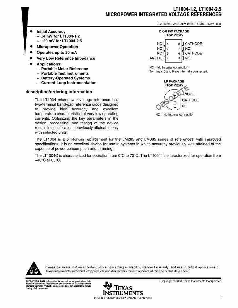
Initial Accuracy− ±4 mV for LT1004-1.2− ±20 mV for LT1004-2.5
Micropower Operation
Operates up to 20 mA
Very Low Reference Impedance
Applications:− Portable Meter Reference− Portable Test Instruments− Battery-Operated Systems− Current-Loop Instrumentation
description/ordering information
The LT1004 micropower voltage reference is atwo-terminal band-gap reference diode designedto provide high accuracy and excellenttemperature characteristics at very low operatingcurrents. Optimizing the key parameters in thedesign, processing, and testing of the deviceresults in specifications previously attainable onlywith selected units.
The LT1004 is a pin-for-pin replacement for the LM285 and LM385 series of references, with improvedspecifications. It is an excellent device for use in systems in which accuracy previously was attained at theexpense of power consumption and trimming.
The LT1004C is characterized for operation from 0°C to 70°C. The LT1004I is characterized for operation from−40°C to 85°C.
Copyright 2008, Texas Instruments IncorporatedPRODUCTION DATA information is current as of publication date.Products conform to specifications per the terms of Texas Instrumentsstandard warranty. Production processing does not necessarily includetesting of all parameters.
Please be aware that an important notice concerning availability, standard warranty, and use in critical applications ofTexas Instruments semiconductor products and disclaimers thereto appears at the end of this data sheet.
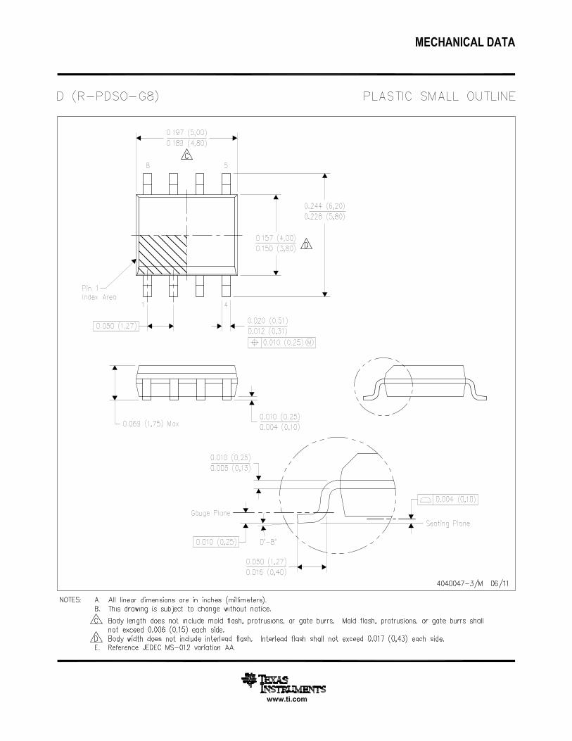
LP PACKAGE(TOP VIEW)
1
2
3
4
8
7
6
5
NCNCNC
ANODE
CATHODENCCATHODENC
D OR PW PACKAGE(TOP VIEW)
ANODE
CATHODE
NC
NC − No internal connectionTerminals 6 and 8 are internally connected.
NC − No internal connection
LT1004-1.2, LT1004-2.5MICROPOWER INTEGRATED VOLTAGE REFERENCES
SLVS022M − JANUARY 1989 − REVISED MAY 2008
2 POST OFFICE BOX 655303 • DALLAS, TEXAS 75265
description/ordering information (continued)
ORDERING INFORMATION
TAVZ
TYP PACKAGE‡ ORDERABLEPART NUMBER
TOP-SIDEMARKING
SOIC (D)Tube of 75 LT1004CD-1-2
4C 12
1 2 V
SOIC (D)Reel of 2500 LT1004CDR-1-2
4C-12
1.2 V
TSSOP (PW)Tube of 150 LT1004CPW-1-2
4C 12
0°C to 70°C
TSSOP (PW)Reel of 2000 LT1004CPWR-1-2
4C-12
0°C to 70°C
SOIC (D)Tube of 75 LT1004CD-2-5
4C 25
2 5 V
SOIC (D)Reel of 2500 LT1004CDR-2-5
4C-25
2.5 V
TSSOP (PW)Tube of 150 LT1004CPW-2-5
4C 25TSSOP (PW)Reel of 2000 LT1004CPWR-2-5
4C-25
SOIC (D)Tube of 75 LT1004ID-1-2
4I 12
1 2 V
SOIC (D)Reel of 2500 LT1004IDR-1-2
4I-12
1.2 V
TSSOP (PW)Tube of 150 LT1004IPW-1-2
4I 12
40°C to 85°CTSSOP (PW)
Reel of 2000 LT1004IPWR-1-24I-12
−40°C to 85°C
SOIC (D)Tube of 75 LT1004ID-2-5
4I 25
2 5 V
SOIC (D)Reel of 2500 LT1004IDR-2-5
4I-25
2.5 V
TSSOP (PW)Tube of 150 LT1004IPW-2-5
4I 25TSSOP (PW)Reel of 2000 LT1004IPWR-2-5
4I-25
† For the most current package and ordering information, see the Package Option Addendum at the end of this document, or seethe TI web site at http://www.ti.com.
‡ Package drawings, thermal data, and symbolization are available at http://www.ti.com/packaging.
symbol
ANODE(A)
CATHODE(K)
LT1004-1.2, LT1004-2.5MICROPOWER INTEGRATED VOLTAGE REFERENCES
SLVS022M − JANUARY 1989 − REVISED MAY 2008
3POST OFFICE BOX 655303 • DALLAS, TEXAS 75265
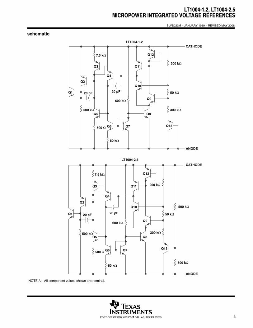
schematic
7.5 kΩ
Q3
Q2
Q1
Q5
Q6
Q11
Q12
Q10
Q9
Q13
Q8
Q7
500 kΩ
500 Ω
60 kΩ
600 kΩ
200 kΩ
50 kΩ
300 kΩ
20 pF 20 pF
ANODE
CATHODE
ANODE
Q13
300 kΩ
50 kΩ
200 kΩ
CATHODE
Q12
Q11
Q10
Q9
Q8
Q7
600 kΩ
20 pF
60 kΩ
500 Ω Q6
Q5500 kΩ
20 pFQ1
Q2
7.5 kΩ
Q3
500 kΩ
500 kΩ
LT1004-2.5
LT1004-1.2
Q4
Q4
NOTE A: All component values shown are nominal.

LT1004-1.2, LT1004-2.5MICROPOWER INTEGRATED VOLTAGE REFERENCES
SLVS022M − JANUARY 1989 − REVISED MAY 2008
4 POST OFFICE BOX 655303 • DALLAS, TEXAS 75265
absolute maximum ratings over operating free-air temperature range (unless otherwise noted)†
Reverse current, IR 30 mA. . . . . . . . . . . . . . . . . . . . . . . . . . . . . . . . . . . . . . . . . . . . . . . . . . . . . . . . . . . . . . . . . . . . . . . Forward current, IF 10 mA. . . . . . . . . . . . . . . . . . . . . . . . . . . . . . . . . . . . . . . . . . . . . . . . . . . . . . . . . . . . . . . . . . . . . . . Package thermal impedance, θJA (see Notes 1 and 2): D package 97°C/W. . . . . . . . . . . . . . . . . . . . . . . . . . . .
PW package 149°C/W. . . . . . . . . . . . . . . . . . . . . . . . . Operating virtual junction temperature, TJ 150°C. . . . . . . . . . . . . . . . . . . . . . . . . . . . . . . . . . . . . . . . . . . . . . . . . . . Lead temperature 1,6 mm (1/16 inch) from case for 10 seconds 260°C. . . . . . . . . . . . . . . . . . . . . . . . . . . . . . . Storage temperature range, Tstg −65°C to 150°C. . . . . . . . . . . . . . . . . . . . . . . . . . . . . . . . . . . . . . . . . . . . . . . . . . .
† Stresses beyond those listed under “absolute maximum ratings” may cause permanent damage to the device. These are stress ratings only, andfunctional operation of the device at these or any other conditions beyond those indicated under “recommended operating conditions” is notimplied. Exposure to absolute-maximum-rated conditions for extended periods may affect device reliability.
NOTES: 1. Maximum power dissipation is a function of TJ(max), θJA, and TA. The maximum allowable power dissipation at any allowableambient temperature is PD = (TJ(max) − TA)/θJA. Operating at the absolute maximum TJ of 150°C can affect reliability.
2. The package thermal impedance is calculated in accordance with JESD 51-7.
recommended operating conditionsMIN MAX UNIT
T Operating free air temperatureLT1004C 0 70
°CTA Operating free-air temperatureLT1004I −40 85
°C
electrical characteristics at specified free-air temperature
PARAMETERTEST
T ‡LT1004-1.2 LT1004-2.5
UNITPARAMETERTEST
CONDITIONS TA‡
MIN TYP MAX MIN TYP MAXUNIT
25°C 1.231 1.235 1.239 2.48 2.5 2.52
VZ Reference voltage IZ = 100 µA Full LT1004C 1.225 1.245 2.47 2.53 VVZ Reference voltage IZ 100 µA Fullrange LT1004I 1.225 1.245 2.47 2.53
V
V
Averagetemperature coefficient
IZ = 10 µA25°C
20ppm/°CVZ
temperature coefficientof reference voltage§ IZ = 20 µA
25°C20
ppm/°C
I I (min) to 1 mA25°C 1 1
∆VChange inreference voltage
IZ = IZ(min) to 1 mAFull range 1.5 1.5
mV∆VZ reference voltagewith current I 1 mA to 20 mA
25°C 10 10mV
with current IZ = 1 mA to 20 mAFull range 20 20
∆VZ/∆tLong-term changein reference voltage
IZ = 100 µA 25°C 20 20 ppm/khr
IZ(min)Minimumreference current
Full range 8 10 12 20 µA
z Reference impedance I 100 A25°C 0.2 0.6 0.2 0.6
Ωzz Reference impedance IZ = 100 µAFull range 1.5 1.5
Ω
VnBroadbandnoise voltage
IZ = 100 µA,f = 10 Hz to 10 kHz
25°C 60 120 µV
‡ Full range is 0°C to 70°C for the LT1004C and −40°C to 85°C for the LT1004I.§ The average temperature coefficient of reference voltage is defined as the total change in reference voltage divided by the specified temperature
range.
LT1004-1.2, LT1004-2.5MICROPOWER INTEGRATED VOLTAGE REFERENCES
SLVS022M − JANUARY 1989 − REVISED MAY 2008
5POST OFFICE BOX 655303 • DALLAS, TEXAS 75265
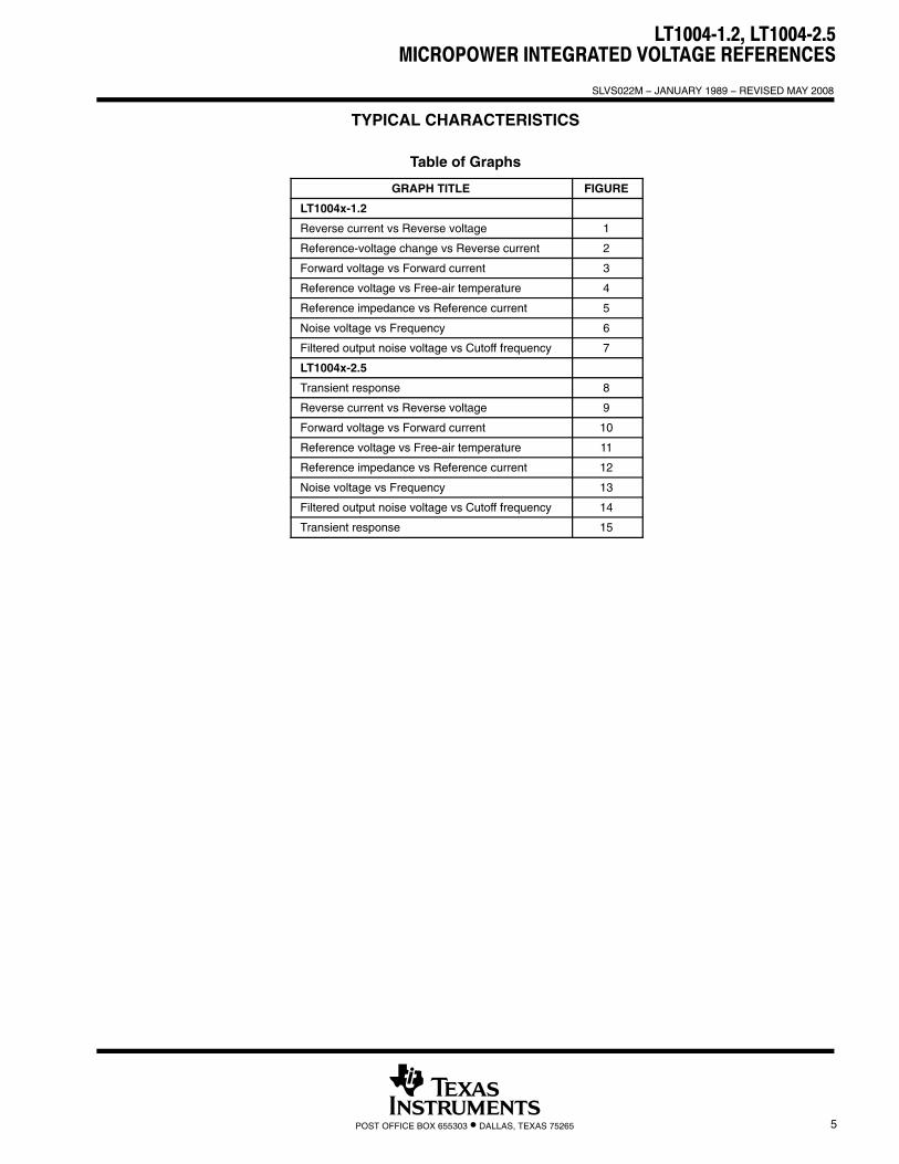
TYPICAL CHARACTERISTICS
Table of Graphs
GRAPH TITLE FIGURE
LT1004x-1.2
Reverse current vs Reverse voltage 1
Reference-voltage change vs Reverse current 2
Forward voltage vs Forward current 3
Reference voltage vs Free-air temperature 4
Reference impedance vs Reference current 5
Noise voltage vs Frequency 6
Filtered output noise voltage vs Cutoff frequency 7
LT1004x-2.5
Transient response 8
Reverse current vs Reverse voltage 9
Forward voltage vs Forward current 10
Reference voltage vs Free-air temperature 11
Reference impedance vs Reference current 12
Noise voltage vs Frequency 13
Filtered output noise voltage vs Cutoff frequency 14
Transient response 15
LT1004-1.2, LT1004-2.5MICROPOWER INTEGRATED VOLTAGE REFERENCES
SLVS022M − JANUARY 1989 − REVISED MAY 2008
6 POST OFFICE BOX 655303 • DALLAS, TEXAS 75265
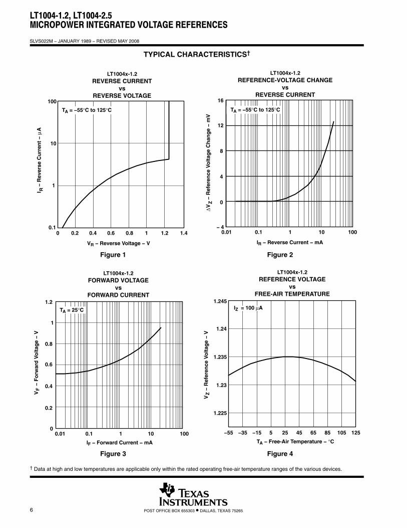
TYPICAL CHARACTERISTICS†
Figure 1
0 0.2 0.4 0.6 0.8 1 1.2 1.4
− R
ever
se C
urr
ent
−
VR − Reverse Voltage − V
0.1
1
10
100
LT1004x-1.2REVERSE CURRENT
vsREVERSE VOLTAGE
I RAµ
ÎÎÎÎÎÎÎÎÎÎÎÎÎÎ
TA = −55°C to 125°C
Figure 2
1010.10.01− 4
0
4
8
12
16
IR − Reverse Current − mA
− R
efer
ence
Vo
ltag
e C
han
ge
− m
V
LT1004x-1.2REFERENCE-VOLTAGE CHANGE
vsREVERSE CURRENT
100
∆V
Z
ÎÎÎÎÎÎÎÎÎÎÎÎ
TA = −55°C to 125°C
Figure 3
0.01 0.1 1 10 100
0.8
1.2
0.4
0
IF − Forward Current − mA
− F
orw
ard
Vo
ltag
e −
V
LT1004x-1.2FORWARD VOLTAGE
vsFORWARD CURRENT
VF
ÎÎÎÎTA = 25°C
1
0.6
0.2
Figure 4
125105856545255−15−35−55
1.225
1.23
1.235
1.24
1.245
TA − Free-Air Temperature − °C
− R
efer
ence
Vo
ltag
e −
V
LT1004x-1.2REFERENCE VOLTAGE
vsFREE-AIR TEMPERATURE
VZ
ÎÎÎÎÎÎÎÎÎÎ
IZ = 100 µA
† Data at high and low temperatures are applicable only within the rated operating free-air temperature ranges of the various devices.
LT1004-1.2, LT1004-2.5MICROPOWER INTEGRATED VOLTAGE REFERENCES
SLVS022M − JANUARY 1989 − REVISED MAY 2008
7POST OFFICE BOX 655303 • DALLAS, TEXAS 75265
TYPICAL CHARACTERISTICS†
Figure 5
LT1004x-1.2REFERENCE IMPEDANCE
vsREFERENCE CURRENT
− R
efer
ence
Imp
edan
ce −
IZ − Reference Current − mA
ÎÎÎÎÎÎÎÎÎÎÎÎÎÎ
f = 25 HzTA = −55°C to 125°C
100
10
1
0.11001010.10.01
Ωz
z
Figure 6
LT1004x-1.2NOISE VOLTAGE
vsFREQUENCY
− N
ois
e Vo
ltag
e −
f − Frequency − Hz
700
600
500
400
300
200
100
010 100 1 k 10 k 100 k
Vn
nV
/H
z
ÎÎÎÎÎÎÎÎ
IZ = 100 µA
ÎÎÎÎTA = 25°C
Figure 7
Filt
ered
Ou
tpu
t N
ois
e Vo
ltag
e −
Cutoff Frequency − kHz
1001010.1
70
60
50
40
30
20
10
0
TL1004x-1.2FILTERED OUTPUT NOISE VOLTAGE
vsCUTOFF FREQUENCY
µV
C
R100 µA
ÎÎÎÎÎÎÎÎÎÎ
RC Low PassÎÎÎÎÎIZ = 100 µAÎÎÎÎÎÎÎÎÎÎ
TA = 25°C
Figure 8
ÎÎÎÎOutput
1.5
1
0.5
0
5
06005001000
Inp
ut
and
Ou
tpu
t Vo
ltag
es −
V
t − Time − µs
ÎÎÎInput
LT1004x-1.2TRANSIENT RESPONSE
36 kΩVOVI
2
† Data at high and low temperatures are applicable only within the rated operating free-air temperature ranges of the various devices.
LT1004-1.2, LT1004-2.5MICROPOWER INTEGRATED VOLTAGE REFERENCES
SLVS022M − JANUARY 1989 − REVISED MAY 2008
8 POST OFFICE BOX 655303 • DALLAS, TEXAS 75265
TYPICAL CHARACTERISTICS†
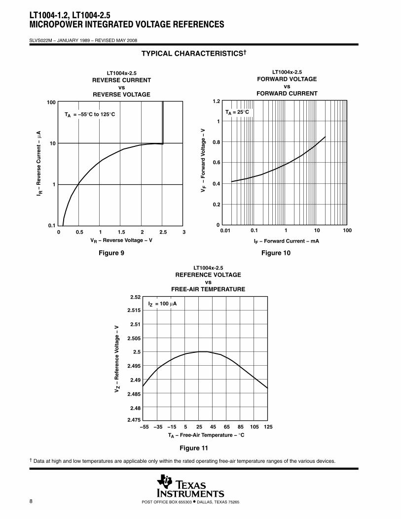
Figure 9
VR − Reverse Voltage − V
ÎÎÎÎÎÎTA = −55°C to 125°C
100
10
1
0.132.521.510.50
LT1004x-2.5REVERSE CURRENT
vsREVERSE VOLTAGE
− R
ever
se C
urr
ent
−I R
Aµ
Figure 10
1.2
0.8
0.4
1001010.10.010
ÎÎÎÎÎÎÎÎ
TA = 25°C
IF − Forward Current − mA
LT1004x-2.5FORWARD VOLTAGE
vsFORWARD CURRENT
− F
orw
ard
Vo
ltag
e −
VV
F
1
0.6
0.2
2.515
2.51
2.505
2.5
2.495
2.48
2.485
125105856545255−15−35
2.49
TA − Free-Air Temperature − °C−55
LT1004x-2.5REFERENCE VOLTAGE
vsFREE-AIR TEMPERATURE
− R
efer
ence
Vo
ltag
e −
VV
Z
2.52
2.475
ÎÎÎÎÎÎÎÎÎÎ
IZ = 100 µA
Figure 11
† Data at high and low temperatures are applicable only within the rated operating free-air temperature ranges of the various devices.
LT1004-1.2, LT1004-2.5MICROPOWER INTEGRATED VOLTAGE REFERENCES
SLVS022M − JANUARY 1989 − REVISED MAY 2008
9POST OFFICE BOX 655303 • DALLAS, TEXAS 75265
TYPICAL CHARACTERISTICS†
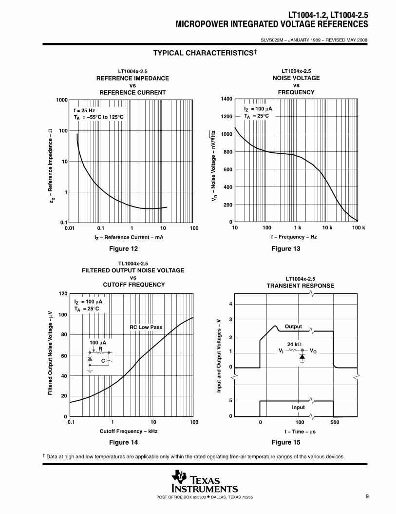
Figure 12
100
10
1
IZ − Reference Current − mA
1000
0.11001010.10.01
− R
efer
ence
Imp
edan
ce −
Ω
LT1004x-2.5REFERENCE IMPEDANCE
vsREFERENCE CURRENT
ÎÎÎÎÎÎÎÎÎÎÎÎÎÎÎÎÎÎ
f = 25 HzTA = −55°C to 125°C
zz
Figure 13
f − Frequency − Hz
1400
1200
1000
800
600
200
010 100 1 k 10 k 100 k
400
− N
ois
e Vo
ltag
e −
Vn
nV
/H
z
ÎÎÎÎÎÎÎÎ
IZ = 100 µA
ÎÎÎÎTA = 25°C
LT1004x-2.5NOISE VOLTAGE
vsFREQUENCY
Figure 14
Cutoff Frequency − kHz
1001010.1
120
100
80
60
40
20
0
TL1004x-2.5FILTERED OUTPUT NOISE VOLTAGE
vs CUTOFF FREQUENCY
Filt
ered
Ou
tpu
t N
ois
e Vo
ltag
e −
µV
C
R100 µA
ÎÎÎÎÎÎÎÎÎÎ
RC Low Pass
ÎÎÎÎIZ = 100 µAÎÎÎÎÎÎÎÎ
TA = 25°C
Figure 15
t − Time − µs
Inp
ut
and
Ou
tpu
t Vo
ltag
es −
V
100 500
Output
Input
LT1004x-2.5TRANSIENT RESPONSE
24 kΩVOVI
0
4
3
2
1
0
5
0
† Data at high and low temperatures are applicable only within the rated operating free-air temperature ranges of the various devices.
LT1004-1.2, LT1004-2.5MICROPOWER INTEGRATED VOLTAGE REFERENCES
SLVS022M − JANUARY 1989 − REVISED MAY 2008
10 POST OFFICE BOX 655303 • DALLAS, TEXAS 75265
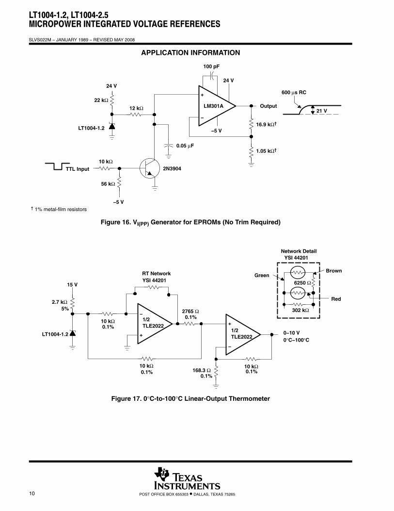
APPLICATION INFORMATION
+
LM301A
24 V
−
100 pF
Output
−5 V16.9 kΩ†
1.05 kΩ†0.05 µF
2N3904
56 kΩ
−5 V
10 kΩTTL Input
12 kΩ
24 V
22 kΩ
LT1004-1.2
21 V
600 µs RC
† 1% metal-film resistors
Figure 16. VI(PP) Generator for EPROMs (No Trim Required)
Brown
Red
Green6250 Ω
302 kΩ
15 V
10 kΩ0.1%
2.7 kΩ5%
LT1004-1.2
2765 Ω0.1%
10 kΩ0.1%
10 kΩ0.1%
0.1%168.3 Ω
0−10 V0°C−100°C
RT NetworkYSI 44201
Network DetailYSI 44201
+1/2TLE2022
−
+
1/2TLE2022
−
Figure 17. 0°C-to-100°C Linear-Output Thermometer
LT1004-1.2, LT1004-2.5MICROPOWER INTEGRATED VOLTAGE REFERENCES
SLVS022M − JANUARY 1989 − REVISED MAY 2008
11POST OFFICE BOX 655303 • DALLAS, TEXAS 75265
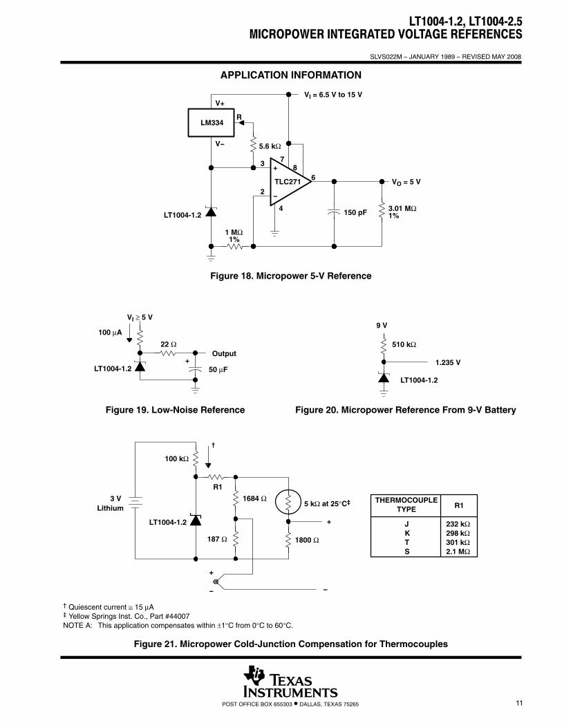
APPLICATION INFORMATION
VI = 6.5 V to 15 VV+
R
V−
LM334
5.6 kΩ
3 78
6
2
4
+
−
TLC271 VO = 5 V
150 pF 3.01 MΩ1%
1%1 MΩ
LT1004-1.2
Figure 18. Micropower 5-V Reference
Figure 19. Low-Noise Reference
Output
50 µF
22 Ω
VI ≥ 5 V
+LT1004-1.2
100 µA
Figure 20. Micropower Reference From 9-V Battery
9 V
510 kΩ
1.235 V
LT1004-1.2
R1
5 kΩ at 25°C‡
1800 Ω
1684 Ω
187 Ω
LT1004-1.2
3 VLithium
+
−
100 kΩ
†
−
+
THERMOCOUPLETYPE R1
JKTS
232 kΩ298 kΩ301 kΩ2.1 MΩ
† Quiescent current ≅ 15 µA‡ Yellow Springs Inst. Co., Part #44007NOTE A: This application compensates within ±1°C from 0°C to 60°C.
Figure 21. Micropower Cold-Junction Compensation for Thermocouples
LT1004-1.2, LT1004-2.5MICROPOWER INTEGRATED VOLTAGE REFERENCES
SLVS022M − JANUARY 1989 − REVISED MAY 2008
12 POST OFFICE BOX 655303 • DALLAS, TEXAS 75265
APPLICATION INFORMATION
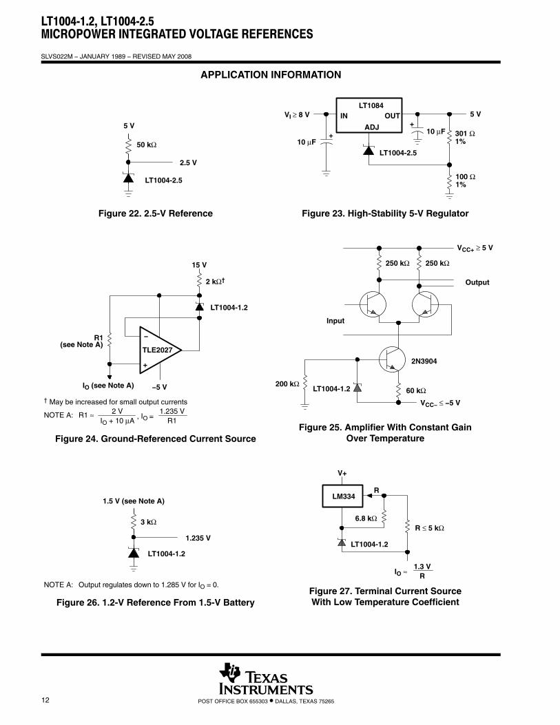
Figure 22. 2.5-V Reference
5 V
50 kΩ
2.5 V
LT1004-2.5
Figure 23. High-Stability 5-V Regulator
+
VI ≥ 8 V
10 µF
IN OUTLT1084
ADJ
5 V+
10 µF 301 Ω1%
100 Ω1%
LT1004-2.5
Figure 24. Ground-Referenced Current Source
15 V
2 kن
LT1004-1.2
TLE2027
−
+
R1(see Note A)
−5 VIO (see Note A)
† May be increased for small output currents
NOTE A: R1 ≈ 2 VIO + 10 µA
, IO =1.235 V
R1Figure 25. Amplifier With Constant Gain
Over Temperature
VCC+ ≥ 5 V
Output
2N3904
60 kΩ
VCC− ≤ −5 V
250 kΩ250 kΩ
Input
LT1004-1.2200 kΩ
Figure 26. 1.2-V Reference From 1.5-V Battery
1.5 V (see Note A)
3 kΩ
1.235 V
LT1004-1.2
NOTE A: Output regulates down to 1.285 V for IO = 0.Figure 27. Terminal Current SourceWith Low Temperature Coefficient
V+
R
6.8 kΩR ≤ 5 kΩ
LT1004-1.2
LM334
IO ≈1.3 V
R
LT1004-1.2, LT1004-2.5MICROPOWER INTEGRATED VOLTAGE REFERENCES
SLVS022M − JANUARY 1989 − REVISED MAY 2008
13POST OFFICE BOX 655303 • DALLAS, TEXAS 75265
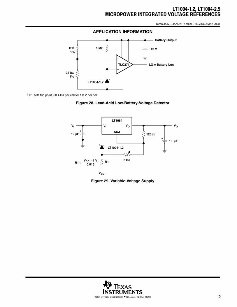
APPLICATION INFORMATION
1 MΩ
Battery Output
12 V
LO = Battery Low
R1†
1%
133 kΩ1%
LT1004-1.2
+
−TLC271
† R1 sets trip point, 60.4 kΩ per cell for 1.8 V per cell.
Figure 28. Lead-Acid Low-Battery-Voltage Detector
VCC − 1 V0.015
LT1084
ADJ
VI VO VOVI
10 µF
10 µF 120 Ω
LT1004-1.2
2 kΩ
VCC−
+
+
R1 ≤ R1
Figure 29. Variable-Voltage Supply
PACKAGE OPTION ADDENDUM
www.ti.com 8-Jun-2017
Addendum-Page 1
PACKAGING INFORMATION
Orderable Device Status(1)
Package Type PackageDrawing
Pins PackageQty
Eco Plan(2)
Lead/Ball Finish(6)
MSL Peak Temp(3)
Op Temp (°C) Device Marking(4/5)
Samples
LT1004CD-1-2 ACTIVE SOIC D 8 75 Green (RoHS& no Sb/Br)
CU NIPDAU Level-1-260C-UNLIM 4C-12
LT1004CD-2-5 ACTIVE SOIC D 8 75 Green (RoHS& no Sb/Br)
CU NIPDAU Level-1-260C-UNLIM 4C-25
LT1004CDG4-1-2 ACTIVE SOIC D 8 75 Green (RoHS& no Sb/Br)
CU NIPDAU Level-1-260C-UNLIM 0 to 70 4C-12
LT1004CDR-1-2 ACTIVE SOIC D 8 2500 Green (RoHS& no Sb/Br)
CU NIPDAU Level-1-260C-UNLIM 4C-12
LT1004CDR-2-5 ACTIVE SOIC D 8 2500 Green (RoHS& no Sb/Br)
CU NIPDAU Level-1-260C-UNLIM 4C-25
LT1004CDRG4-2-5 ACTIVE SOIC D 8 2500 Green (RoHS& no Sb/Br)
CU NIPDAU Level-1-260C-UNLIM 0 to 70 4C-25
LT1004CPW-1-2 ACTIVE TSSOP PW 8 150 Green (RoHS& no Sb/Br)
CU NIPDAU Level-1-260C-UNLIM -40 to 85 4C-12
LT1004CPWR-1-2 ACTIVE TSSOP PW 8 2000 Green (RoHS& no Sb/Br)
CU NIPDAU Level-1-260C-UNLIM 0 to 70 4C-12
LT1004CPWR-2-5 ACTIVE TSSOP PW 8 2000 Green (RoHS& no Sb/Br)
CU NIPDAU Level-1-260C-UNLIM 0 to 70 4C-25
LT1004ID-1-2 ACTIVE SOIC D 8 75 Green (RoHS& no Sb/Br)
CU NIPDAU Level-1-260C-UNLIM 4I-12
LT1004ID-2-5 ACTIVE SOIC D 8 75 Green (RoHS& no Sb/Br)
CU NIPDAU Level-1-260C-UNLIM 4I-25
LT1004IDG4-1-2 ACTIVE SOIC D 8 75 Green (RoHS& no Sb/Br)
CU NIPDAU Level-1-260C-UNLIM -40 to 85 4I-12
LT1004IDG4-2-5 ACTIVE SOIC D 8 75 Green (RoHS& no Sb/Br)
CU NIPDAU Level-1-260C-UNLIM -40 to 85 4I-25
LT1004IDR-1-2 ACTIVE SOIC D 8 2500 Green (RoHS& no Sb/Br)
CU NIPDAU Level-1-260C-UNLIM -40 to 85 4I-12
LT1004IDR-2-5 ACTIVE SOIC D 8 2500 Green (RoHS& no Sb/Br)
CU NIPDAU Level-1-260C-UNLIM 4I-25
LT1004IDRE4-2-5 ACTIVE SOIC D 8 2500 Green (RoHS& no Sb/Br)
CU NIPDAU Level-1-260C-UNLIM -40 to 85 4I-25
LT1004IDRG4-1-2 ACTIVE SOIC D 8 2500 Green (RoHS& no Sb/Br)
CU NIPDAU Level-1-260C-UNLIM -40 to 85 4I-12
PACKAGE OPTION ADDENDUM
www.ti.com 8-Jun-2017
Addendum-Page 2
Orderable Device Status(1)
Package Type PackageDrawing
Pins PackageQty
Eco Plan(2)
Lead/Ball Finish(6)
MSL Peak Temp(3)
Op Temp (°C) Device Marking(4/5)
Samples
LT1004IPW-1-2 ACTIVE TSSOP PW 8 150 Green (RoHS& no Sb/Br)
CU NIPDAU Level-1-260C-UNLIM -40 to 85 4I-12
LT1004IPW-2-5 ACTIVE TSSOP PW 8 150 Green (RoHS& no Sb/Br)
CU NIPDAU Level-1-260C-UNLIM -40 to 85 4I-25
LT1004IPWR-1-2 ACTIVE TSSOP PW 8 2000 Green (RoHS& no Sb/Br)
CU NIPDAU Level-1-260C-UNLIM -40 to 85 4I-12
LT1004IPWR-2-5 ACTIVE TSSOP PW 8 2000 Green (RoHS& no Sb/Br)
CU NIPDAU Level-1-260C-UNLIM -40 to 85 4I-25
(1) The marketing status values are defined as follows:ACTIVE: Product device recommended for new designs.LIFEBUY: TI has announced that the device will be discontinued, and a lifetime-buy period is in effect.NRND: Not recommended for new designs. Device is in production to support existing customers, but TI does not recommend using this part in a new design.PREVIEW: Device has been announced but is not in production. Samples may or may not be available.OBSOLETE: TI has discontinued the production of the device.
(2) RoHS: TI defines "RoHS" to mean semiconductor products that are compliant with the current EU RoHS requirements for all 10 RoHS substances, including the requirement that RoHS substancedo not exceed 0.1% by weight in homogeneous materials. Where designed to be soldered at high temperatures, "RoHS" products are suitable for use in specified lead-free processes. TI mayreference these types of products as "Pb-Free".RoHS Exempt: TI defines "RoHS Exempt" to mean products that contain lead but are compliant with EU RoHS pursuant to a specific EU RoHS exemption.Green: TI defines "Green" to mean the content of Chlorine (Cl) and Bromine (Br) based flame retardants meet JS709B low halogen requirements of <=1000ppm threshold. Antimony trioxide basedflame retardants must also meet the <=1000ppm threshold requirement.
(3) MSL, Peak Temp. - The Moisture Sensitivity Level rating according to the JEDEC industry standard classifications, and peak solder temperature.
(4) There may be additional marking, which relates to the logo, the lot trace code information, or the environmental category on the device.
(5) Multiple Device Markings will be inside parentheses. Only one Device Marking contained in parentheses and separated by a "~" will appear on a device. If a line is indented then it is a continuationof the previous line and the two combined represent the entire Device Marking for that device.
(6) Lead/Ball Finish - Orderable Devices may have multiple material finish options. Finish options are separated by a vertical ruled line. Lead/Ball Finish values may wrap to two lines if the finishvalue exceeds the maximum column width.
Important Information and Disclaimer:The information provided on this page represents TI's knowledge and belief as of the date that it is provided. TI bases its knowledge and belief on informationprovided by third parties, and makes no representation or warranty as to the accuracy of such information. Efforts are underway to better integrate information from third parties. TI has taken andcontinues to take reasonable steps to provide representative and accurate information but may not have conducted destructive testing or chemical analysis on incoming materials and chemicals.TI and TI suppliers consider certain information to be proprietary, and thus CAS numbers and other limited information may not be available for release.
PACKAGE OPTION ADDENDUM
www.ti.com 8-Jun-2017
Addendum-Page 3
In no event shall TI's liability arising out of such information exceed the total purchase price of the TI part(s) at issue in this document sold by TI to Customer on an annual basis.
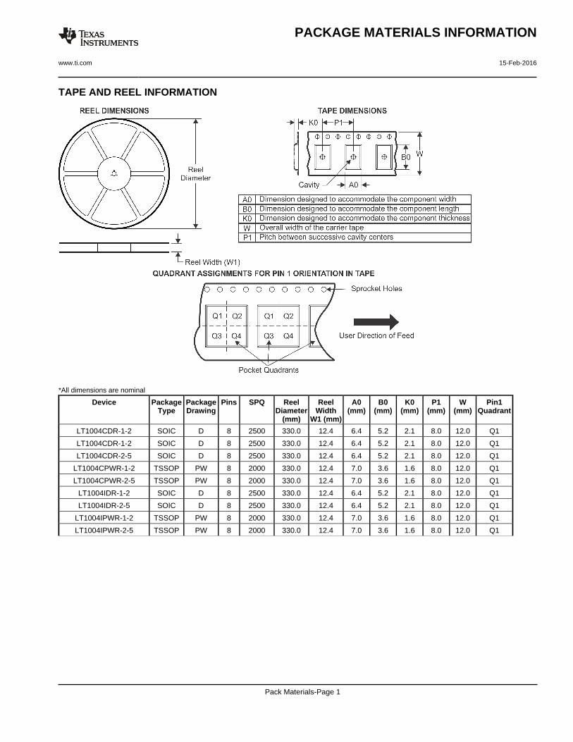
TAPE AND REEL INFORMATION
*All dimensions are nominal
Device PackageType
PackageDrawing
Pins SPQ ReelDiameter
(mm)
ReelWidth
W1 (mm)
A0(mm)
B0(mm)
K0(mm)
P1(mm)
W(mm)
Pin1Quadrant
LT1004CDR-1-2 SOIC D 8 2500 330.0 12.4 6.4 5.2 2.1 8.0 12.0 Q1
LT1004CDR-1-2 SOIC D 8 2500 330.0 12.4 6.4 5.2 2.1 8.0 12.0 Q1
LT1004CDR-2-5 SOIC D 8 2500 330.0 12.4 6.4 5.2 2.1 8.0 12.0 Q1
LT1004CPWR-1-2 TSSOP PW 8 2000 330.0 12.4 7.0 3.6 1.6 8.0 12.0 Q1
LT1004CPWR-2-5 TSSOP PW 8 2000 330.0 12.4 7.0 3.6 1.6 8.0 12.0 Q1
LT1004IDR-1-2 SOIC D 8 2500 330.0 12.4 6.4 5.2 2.1 8.0 12.0 Q1
LT1004IDR-2-5 SOIC D 8 2500 330.0 12.4 6.4 5.2 2.1 8.0 12.0 Q1
LT1004IPWR-1-2 TSSOP PW 8 2000 330.0 12.4 7.0 3.6 1.6 8.0 12.0 Q1
LT1004IPWR-2-5 TSSOP PW 8 2000 330.0 12.4 7.0 3.6 1.6 8.0 12.0 Q1
PACKAGE MATERIALS INFORMATION
www.ti.com 15-Feb-2016
Pack Materials-Page 1
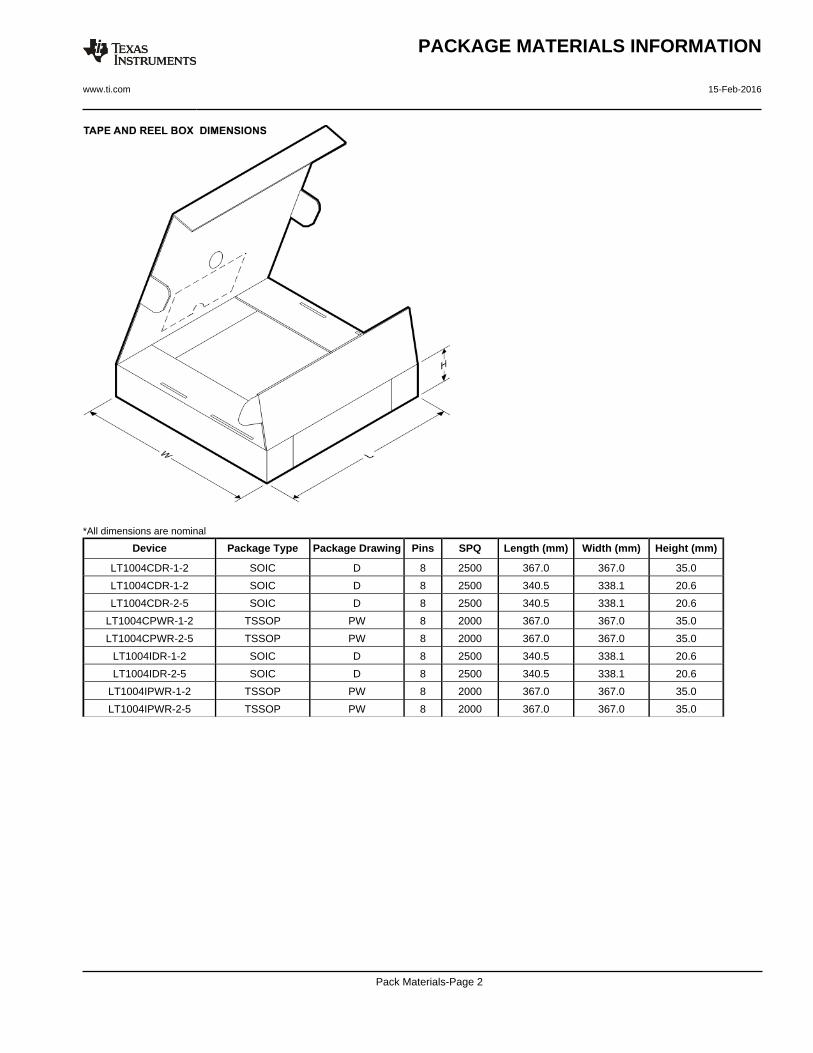
*All dimensions are nominal
Device Package Type Package Drawing Pins SPQ Length (mm) Width (mm) Height (mm)
LT1004CDR-1-2 SOIC D 8 2500 367.0 367.0 35.0
LT1004CDR-1-2 SOIC D 8 2500 340.5 338.1 20.6
LT1004CDR-2-5 SOIC D 8 2500 340.5 338.1 20.6
LT1004CPWR-1-2 TSSOP PW 8 2000 367.0 367.0 35.0
LT1004CPWR-2-5 TSSOP PW 8 2000 367.0 367.0 35.0
LT1004IDR-1-2 SOIC D 8 2500 340.5 338.1 20.6
LT1004IDR-2-5 SOIC D 8 2500 340.5 338.1 20.6
LT1004IPWR-1-2 TSSOP PW 8 2000 367.0 367.0 35.0
LT1004IPWR-2-5 TSSOP PW 8 2000 367.0 367.0 35.0
PACKAGE MATERIALS INFORMATION
www.ti.com 15-Feb-2016
Pack Materials-Page 2
www.ti.com
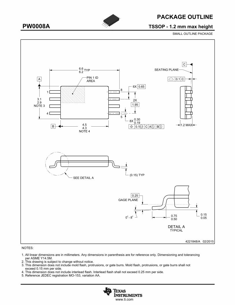
PACKAGE OUTLINE
C
TYP6.66.2
1.2 MAX
6X 0.65
8X 0.300.19
2X1.95
0.150.05
(0.15) TYP
0 - 8
0.25GAGE PLANE
0.750.50
A
NOTE 3
3.12.9
BNOTE 4
4.54.3
4221848/A 02/2015
TSSOP - 1.2 mm max heightPW0008ASMALL OUTLINE PACKAGE
NOTES: 1. All linear dimensions are in millimeters. Any dimensions in parenthesis are for reference only. Dimensioning and tolerancing per ASME Y14.5M. 2. This drawing is subject to change without notice. 3. This dimension does not include mold flash, protrusions, or gate burrs. Mold flash, protrusions, or gate burrs shall not exceed 0.15 mm per side. 4. This dimension does not include interlead flash. Interlead flash shall not exceed 0.25 mm per side.5. Reference JEDEC registration MO-153, variation AA.
18
0.1 C A B
54
PIN 1 IDAREA
SEATING PLANE
0.1 C
SEE DETAIL A
DETAIL ATYPICAL
SCALE 2.800
www.ti.com
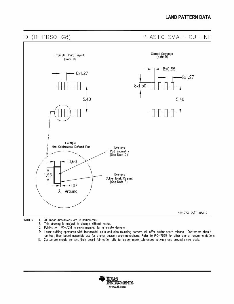
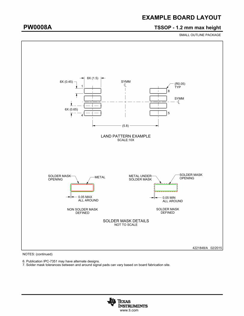
EXAMPLE BOARD LAYOUT
(5.8)
0.05 MAXALL AROUND
0.05 MINALL AROUND
8X (1.5)8X (0.45)
6X (0.65)
(R )TYP
0.05
4221848/A 02/2015
TSSOP - 1.2 mm max heightPW0008ASMALL OUTLINE PACKAGE
SYMM
SYMM
LAND PATTERN EXAMPLESCALE:10X
1
45
8
NOTES: (continued) 6. Publication IPC-7351 may have alternate designs. 7. Solder mask tolerances between and around signal pads can vary based on board fabrication site.
METALSOLDER MASKOPENING
NON SOLDER MASKDEFINED
SOLDER MASK DETAILSNOT TO SCALE
SOLDER MASKOPENING
METAL UNDERSOLDER MASK
SOLDER MASKDEFINED
www.ti.com
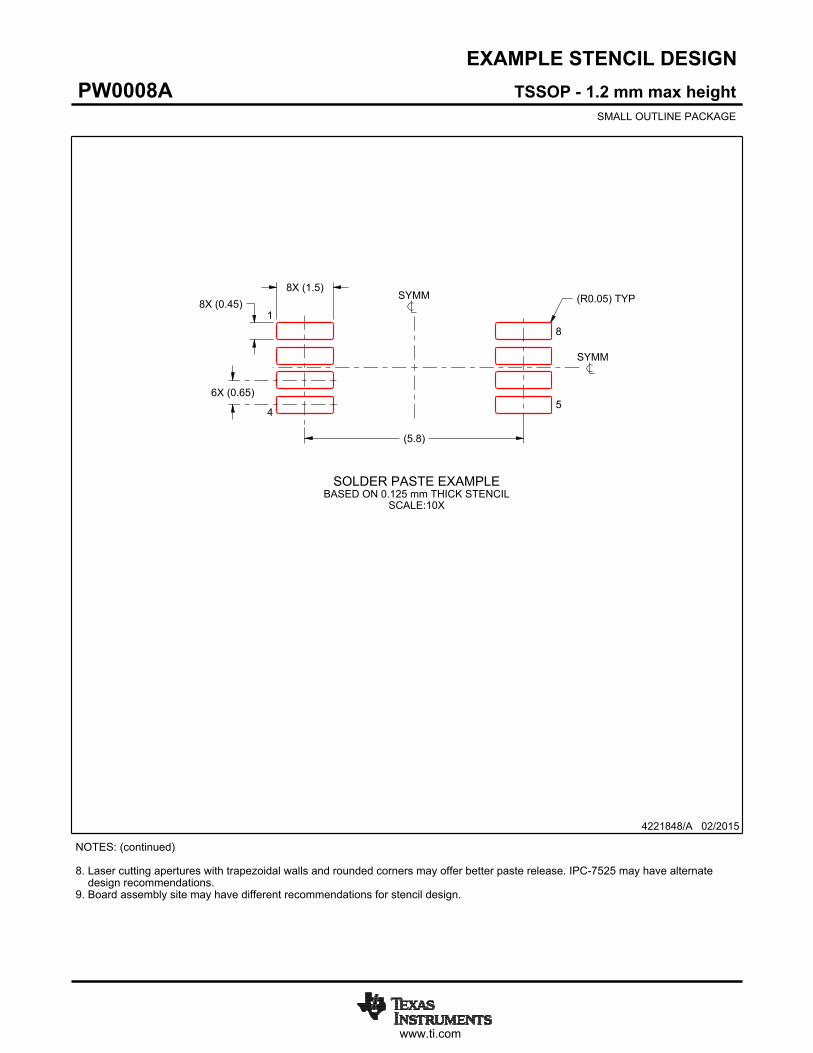
EXAMPLE STENCIL DESIGN
(5.8)
6X (0.65)
8X (0.45)8X (1.5)
(R ) TYP0.05
4221848/A 02/2015
TSSOP - 1.2 mm max heightPW0008ASMALL OUTLINE PACKAGE
NOTES: (continued) 8. Laser cutting apertures with trapezoidal walls and rounded corners may offer better paste release. IPC-7525 may have alternate design recommendations. 9. Board assembly site may have different recommendations for stencil design.
SYMM
SYMM
1
45
8
SOLDER PASTE EXAMPLEBASED ON 0.125 mm THICK STENCIL
SCALE:10X
IMPORTANT NOTICE
Texas Instruments Incorporated (TI) reserves the right to make corrections, enhancements, improvements and other changes to itssemiconductor products and services per JESD46, latest issue, and to discontinue any product or service per JESD48, latest issue. Buyersshould obtain the latest relevant information before placing orders and should verify that such information is current and complete.TI’s published terms of sale for semiconductor products (http://www.ti.com/sc/docs/stdterms.htm) apply to the sale of packaged integratedcircuit products that TI has qualified and released to market. Additional terms may apply to the use or sale of other types of TI products andservices.Reproduction of significant portions of TI information in TI data sheets is permissible only if reproduction is without alteration and isaccompanied by all associated warranties, conditions, limitations, and notices. TI is not responsible or liable for such reproduceddocumentation. Information of third parties may be subject to additional restrictions. Resale of TI products or services with statementsdifferent from or beyond the parameters stated by TI for that product or service voids all express and any implied warranties for theassociated TI product or service and is an unfair and deceptive business practice. TI is not responsible or liable for any such statements.Buyers and others who are developing systems that incorporate TI products (collectively, “Designers”) understand and agree that Designersremain responsible for using their independent analysis, evaluation and judgment in designing their applications and that Designers havefull and exclusive responsibility to assure the safety of Designers' applications and compliance of their applications (and of all TI productsused in or for Designers’ applications) with all applicable regulations, laws and other applicable requirements. Designer represents that, withrespect to their applications, Designer has all the necessary expertise to create and implement safeguards that (1) anticipate dangerousconsequences of failures, (2) monitor failures and their consequences, and (3) lessen the likelihood of failures that might cause harm andtake appropriate actions. Designer agrees that prior to using or distributing any applications that include TI products, Designer willthoroughly test such applications and the functionality of such TI products as used in such applications.TI’s provision of technical, application or other design advice, quality characterization, reliability data or other services or information,including, but not limited to, reference designs and materials relating to evaluation modules, (collectively, “TI Resources”) are intended toassist designers who are developing applications that incorporate TI products; by downloading, accessing or using TI Resources in anyway, Designer (individually or, if Designer is acting on behalf of a company, Designer’s company) agrees to use any particular TI Resourcesolely for this purpose and subject to the terms of this Notice.TI’s provision of TI Resources does not expand or otherwise alter TI’s applicable published warranties or warranty disclaimers for TIproducts, and no additional obligations or liabilities arise from TI providing such TI Resources. TI reserves the right to make corrections,enhancements, improvements and other changes to its TI Resources. TI has not conducted any testing other than that specificallydescribed in the published documentation for a particular TI Resource.Designer is authorized to use, copy and modify any individual TI Resource only in connection with the development of applications thatinclude the TI product(s) identified in such TI Resource. NO OTHER LICENSE, EXPRESS OR IMPLIED, BY ESTOPPEL OR OTHERWISETO ANY OTHER TI INTELLECTUAL PROPERTY RIGHT, AND NO LICENSE TO ANY TECHNOLOGY OR INTELLECTUAL PROPERTYRIGHT OF TI OR ANY THIRD PARTY IS GRANTED HEREIN, including but not limited to any patent right, copyright, mask work right, orother intellectual property right relating to any combination, machine, or process in which TI products or services are used. Informationregarding or referencing third-party products or services does not constitute a license to use such products or services, or a warranty orendorsement thereof. Use of TI Resources may require a license from a third party under the patents or other intellectual property of thethird party, or a license from TI under the patents or other intellectual property of TI.TI RESOURCES ARE PROVIDED “AS IS” AND WITH ALL FAULTS. TI DISCLAIMS ALL OTHER WARRANTIES ORREPRESENTATIONS, EXPRESS OR IMPLIED, REGARDING RESOURCES OR USE THEREOF, INCLUDING BUT NOT LIMITED TOACCURACY OR COMPLETENESS, TITLE, ANY EPIDEMIC FAILURE WARRANTY AND ANY IMPLIED WARRANTIES OFMERCHANTABILITY, FITNESS FOR A PARTICULAR PURPOSE, AND NON-INFRINGEMENT OF ANY THIRD PARTY INTELLECTUALPROPERTY RIGHTS. TI SHALL NOT BE LIABLE FOR AND SHALL NOT DEFEND OR INDEMNIFY DESIGNER AGAINST ANY CLAIM,INCLUDING BUT NOT LIMITED TO ANY INFRINGEMENT CLAIM THAT RELATES TO OR IS BASED ON ANY COMBINATION OFPRODUCTS EVEN IF DESCRIBED IN TI RESOURCES OR OTHERWISE. IN NO EVENT SHALL TI BE LIABLE FOR ANY ACTUAL,DIRECT, SPECIAL, COLLATERAL, INDIRECT, PUNITIVE, INCIDENTAL, CONSEQUENTIAL OR EXEMPLARY DAMAGES INCONNECTION WITH OR ARISING OUT OF TI RESOURCES OR USE THEREOF, AND REGARDLESS OF WHETHER TI HAS BEENADVISED OF THE POSSIBILITY OF SUCH DAMAGES.Unless TI has explicitly designated an individual product as meeting the requirements of a particular industry standard (e.g., ISO/TS 16949and ISO 26262), TI is not responsible for any failure to meet such industry standard requirements.Where TI specifically promotes products as facilitating functional safety or as compliant with industry functional safety standards, suchproducts are intended to help enable customers to design and create their own applications that meet applicable functional safety standardsand requirements. Using products in an application does not by itself establish any safety features in the application. Designers mustensure compliance with safety-related requirements and standards applicable to their applications. Designer may not use any TI products inlife-critical medical equipment unless authorized officers of the parties have executed a special contract specifically governing such use.Life-critical medical equipment is medical equipment where failure of such equipment would cause serious bodily injury or death (e.g., lifesupport, pacemakers, defibrillators, heart pumps, neurostimulators, and implantables). Such equipment includes, without limitation, allmedical devices identified by the U.S. Food and Drug Administration as Class III devices and equivalent classifications outside the U.S.TI may expressly designate certain products as completing a particular qualification (e.g., Q100, Military Grade, or Enhanced Product).Designers agree that it has the necessary expertise to select the product with the appropriate qualification designation for their applicationsand that proper product selection is at Designers’ own risk. Designers are solely responsible for compliance with all legal and regulatoryrequirements in connection with such selection.Designer will fully indemnify TI and its representatives against any damages, costs, losses, and/or liabilities arising out of Designer’s non-compliance with the terms and provisions of this Notice.
Mailing Address: Texas Instruments, Post Office Box 655303, Dallas, Texas 75265Copyright © 2017, Texas Instruments Incorporated